

Panasonic X70 Service Manual
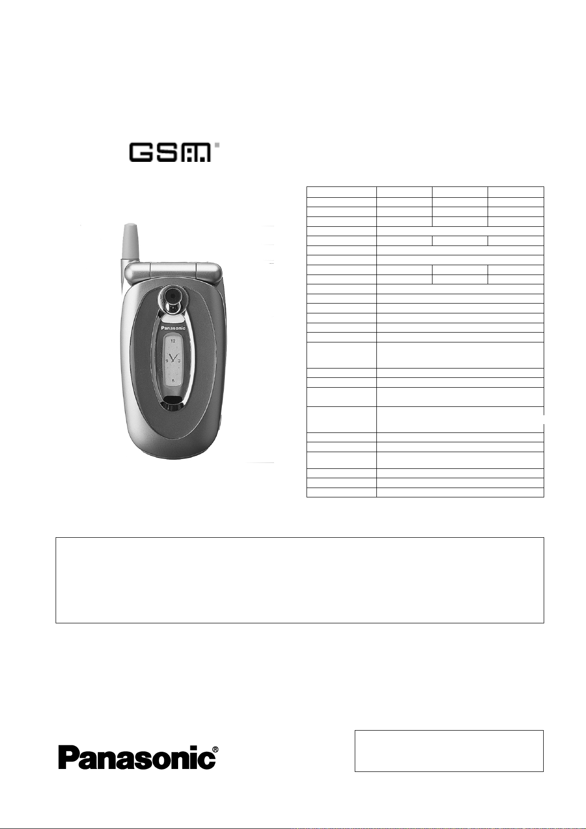
Order Number: PMCD030901C8
Service Manual
Digital Cellular Phone
EB-X70
900 MHz 1800 MHz 1900 MHz
Tx Frequency Range: 880 - 915MHz
Rx Frequency Range: 925 - 960 MHz
Tx / R x sepa ration 45 MHz 95 MHz
RF Channel Bandwidth 200 kHz
Number of RF channels 174 374
Speech coding Full rate/Half rate/Enhanced Full rate
Operating temperature -10 °C to +55 °C
Type Class 4 Handheld Class 1 Handheld
RF Output Power 2 W maximum 1 W maximum
Modulation GMSK (BT = 0.3)
Connection 8 ch / TDMA
Voice digitizing 13 kbps RPE-LTP / 13 kps ACLEP / 5.6 kps CELP / VSLEP
Transmission speed 270.833 kbps
Signal Reception Direct conversion
Antenna VSWR < 2.1 : 1
Dimensions Height: 87.3 mm
(excluding Width: 47.1 mm
antenna) Depth: 24 mm
Volum e 80 c c
Weight 95 g
Main Display LCD, 176 x 132 pixels, 65,536 colours
Sub Display LCD, 96 x 28 pixels, monochrome
Illumination
Keys 17-key Keypad, Navigation key, 1 memo key
SIM
External DC Supply
Voltage
Battery 3.7 V nominal, 680mAh, Li-Ion
Standby Time
Ta lk Ti m e
Talk and standby time will be dependent on network conditions, SIM card, backlight usage
and network condition.
10 LEDs for Keypad Backlighting (White)
4 LEDs for LCD Backlighting (White)
3 LEDs for Sub LCD (Blue, Green, Orange)
3 V Plug-in type only
5.8 V
1710 -1785 MHz 1850 - 1910 MHz
1805 -1880 MHz 1910 - 1990 MHz
60 MHz
299
Class 1 Handheld
1W maximum
WARNING
This service information is designed for experienced repair technicians only and is not designed for use by the general
public. It does not contain warnings or cautions to advise non-technical individuals of potential dangers in attempting to
service a product.
Products powered by electricity should be serviced or repaired only by experienced professional technicians. Any attempt to
service or repair the product or products dealt with in this service manual by anyone else could result in serious injury or
death.
© 2003 Panasonic Mobile Communications
Development of Europe Ltd. All rights reserved.
Unauthorized copying and distribution is a violation
of law.
Issue 1
Revision 0

COMPANY LIABILITY
Every care has been taken to ensure that the contents of this manual give an accurate representation of the equipment.
However, Panasonic Mobile Communications Development of Europe Ltd. accepts no responsibility for inaccuracies which
may occur and reserves the right to make changes to the specification or design without prior notice.
The information contained in this manual and all rights in any design disclosed therein, are and remain the exclusive property
of Panasonic Mobile Communications Development of Europe Ltd.
Other patents applying to material contained in this publication:
CP8 PATENTS
Comments or correspondence concerning this manual should be addressed to:
Panasonic Mobile Communications Development of Europe Ltd.,
2 Gables Way
Thatcham,
Berkshire.
RG19 4ZB.
ENGLAND
CONTENTS
Page Page
1 INTRODUCTION 1
1.1 Purpose of this Manual 1
1.2 Structure of the Manual 2
1.3 Servicing Responsibilities 2
2 GENERAL DESCRIPTION 3
2.1 General 3
2.2 Features 3
2.3 Telephone Handset Main Kit 3
3 OPERATING INSTRUCTIONS 4
3.1 General 4
3.2 Controls and Indicators 4
3.3 Liquid Crystal Displays 5
3.4 Alpha Entry 5
3.5 Features Menu Structure 6
3.6 IMEI and Software Identification 7
3.7 SIM Personalisation 7
4 TECHNICAL DESCRIPTION 9
4.1 RF Overview 9
4.2 Transmitter 11
4.3 Receiver 12
4.4 Baseband Overview 13
4.5 CALYPSO+ 16
4.6 SYREN 18
4.7 Bluetooth Module 19
4.8 Power Supplies 20
5 REPAIR PROCEDURES 25
5.1 Introduction 25
5.2 Underfill Resin Paste 25
5.3 Lead Free (PbF) solder 25
5.4 Jigs and Tools 26
5.5 Using the Channel Box software 28
6 DISASSEMBLY / REASSEMBLY 29
6.1 General 29
6.2 Disassembly 30
6.3 Reassembly 35
7 INTERFACES AND TEST POINTS 39
7.1 Interfaces 39
7.2 Test Points 44
8 FAULT FINDING 46
8.1 RF Waveforms 46
8.2 BGA Fault Identification 48
8.3 Power on fault analysis 49
9 CALIBRATION PROCEDURES 51
9.1 Introduction 51
9.2 Carrier Power Calibration 51
9.3 RSSI 54
9.4 Battery Calibration 55
9.5 Camera Calibration 56
10 REPLACEMENT PARTS LIST 57
10.1 Sub-Assemblies 57
10.2 Main PCB Variants 59
10.3 Language Packs 59
10.4 Main PCB Components 59
10.5 Display PCB 63
10.6 Bulk Pack items 64
10.7 Jigs and Tools 64
10.8 Document Packs 64
11 CIRCUIT DIAGRAMS 65
12 LAYOUT DIAGRAMS 74
Issue 1 – ii – PMCD030901C8
Revision 0 Service Manual

INTRODUCTION
1 INTRODUCTION
WARNING
The equipment described in this manual contains polarised capacitors utilising liquid electrolyte. These devices are
entirely safe provided that neither a short-circuit or a reverse polarity connection is made across the capacitor terminals.
FAILURE TO OBSERVE THIS WARNING COULD RESULT IN DAMAGE TO THE EQUIPMENT OR, AT WORST,
POSSIBLE INJURY TO PERSONNEL RESULTING FROM ELECTRIC SHOCK OR THE AFFECTED CAPACITOR
EXPLODING. EXTREME CARE MUST BE EXERCISED AT ALL TIMES WHEN HANDLING THESE DEVICES.
WARNING
A Naphthalene-based resin paste is used to bond underfill components on this phone. When heated, this paste may give
off traces of Naphthalene.
Therefore, it is recommended that work on the PCB be carried out in a well-ventilated area, especially when using hot air
blowers or soldering irons.
The following components are bonded using the paste:.
CALYPSO+ (U100).
SYREN (U120)
Bluetooth IC (U500)
Caution
The equipment described in this manual contains devices sensitive to electrostatic discharge (ESD). Damage can occur
to these devices if the handling procedures described in this manual are not adhered to.
Caution
This equipment contains an internal battery in addition to the external battery packs. These batteries are recyclable and
should be disposed of in accordance with local legislation. They must not be incinerated, or disposed of as ordinary
rubbish.
Caution
The equipment uses a Printed Circuit Board PCB manufactured using Lead Free (PbF) solder. The procedures described
in this manual should be adhered to when repairing these items.
1.1. Purpose of this Manual
This Service Manual contains the information and procedures required for installing, operating and servicing the Panasonic
GSM Personal Cellular Mobile Telephone system operating on GSM Digital Cellular Networks.
PMCD030901C8 Section 1 Issue 1
Service Manual – 1 – Revision 0

INTRODUCTION
1.2. Structure of the Manual
The manual is structured to provide service engineering personnel with the following information and procedures:
1. General and technical information - provides a basic understanding of the equipment, kits and options, together with
detailed information for each of the major component parts.
2. Installation and operating information - provides instructions for unpacking, installing and operating the equipment.
3. Servicing information - provides complete instructions for the testing, disassembly, repair and reassembly of each major
component part. Step-by-step troubleshooting information is given to enable the isolation and identification of a
malfunction, and thus determine what corrective action should be taken. The test information enables verification of the
integrity of the equipment after any remedial action has been carried out.
4. Illustrated parts list - provided to enable the identification of all equipment components, for the ordering of spare /
replacement parts.
1.3. Servicing Responsibilities
The procedures described in this manual must be performed by qualified service engineering personnel, at an authorised
service centre.
The service engineering personnel are responsible for fault diagnosis and repair of all equipment described in this manual.
Issue 1 Section 1 PMCD030901C8
Revision 0 – 2 – Service Manual
GENERALDESCRIPTION
Service Manual
– 3 –
Revision 0
2 GENERALDESCRIPTION
2.1. General
This section provides a general description and kit composition details for the Digital Cellular Phone and optional kits.
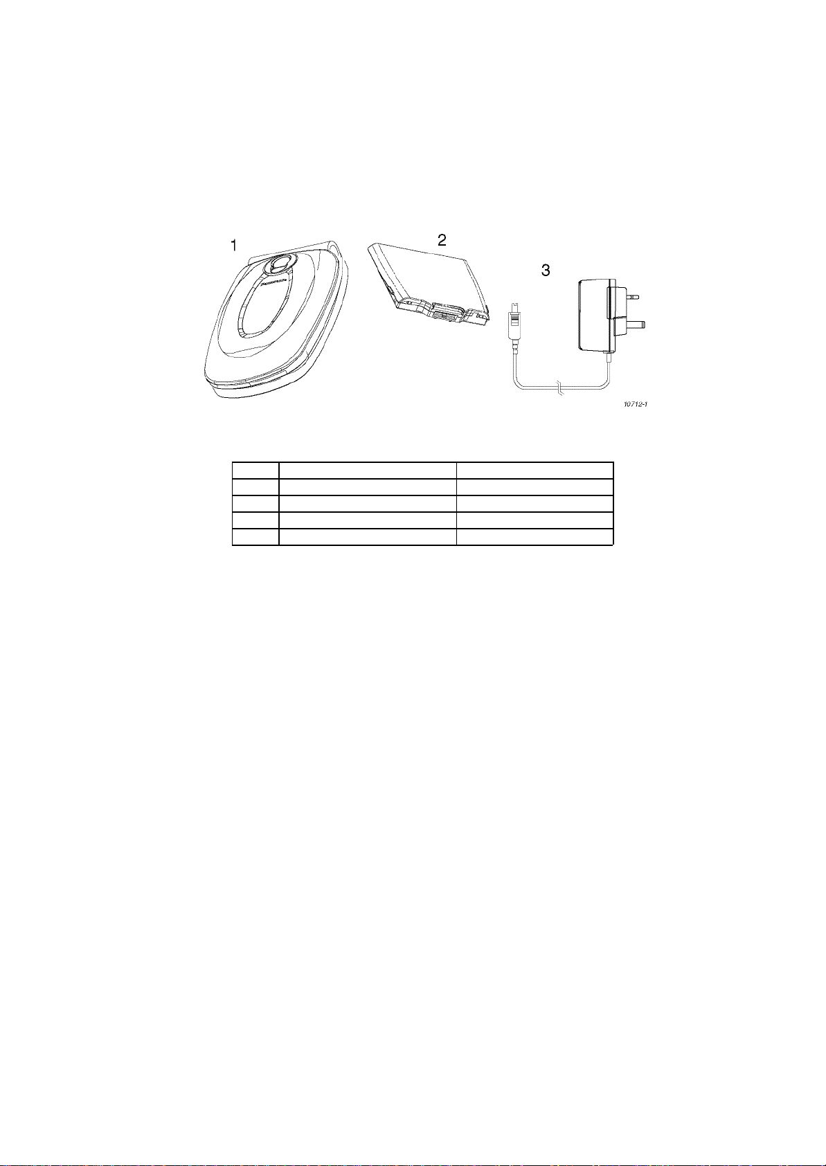
2.2. Telephone Handset Main Kit
Figure 2.1: Telephone Handset Main Unit Kit Contents
ITEM DESCRIPTION PART NUMBER
1 Main Unit EB-X70
2 Battery, Standard EB-BSX70
3 Travel Charger EB-CAX70
- User Guide
2.3. Features
The Panasonic Phone Model X70 is a high performance, small, light, telephone handsets for business and domestic use on
General Packet Radio Service (GPRS) running on GSM networks. The following features are provided:
• Triple Band, EGSM900, GSM1800 and GSM1900 operation.
• Triple Rate, which includes Full Rate, Half rate and Enhanced Full Rate (EFR) speech, codec.
• GPRS-compatible (Class8).
• 65,000-colour Thin Film Transistor (TFT) Main Display and monochrome LCD Sub-Display.
• Integral Digital Camera.
• Multimedia Message Service (MMS) and Short Message Service (SMS) messaging.
• POP3-compliant email client.
• Tegic T9 Text Entry.
• Bluetooth connectivity.
• Infrared communications port (IrDA).
• Voice Recorder.
• WAP2.0 and WAP1.2.1 compliant Browser.
• Backup Battery.
• 16-voice polyphonic ringtones.
• Downloadable pictures, animations and polyphonic melody ring tones.
• Clock, Calculator and Unit Converter.
PMCD030901C8 Section 2 Issue 1
OPERATING INSTRUCTIONS
3 OPERATING INSTRUCTIONS
3.1. General
This section provides a brief guide to the operation and facilities available on the telephone handset. Refer to the Operating
Instructions supplied with the telephone for full operational information.
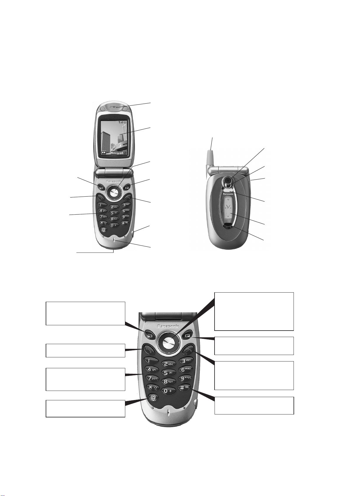
3.2. Controls and Indicators
Earpiece
Main Display
Antenna
Camera Lens
Left Softkey
Call Key
Keypad
Accessory
Connector
Navigation Key
Right Softkey
Power / End Key
Personal Handsfree
connector
Microphone
Self-Portrait
Mirror
Voice Memo /
Camera Shutter
Key
Photolight /
Charge LED /
Camera LED
Sub Display
IrDA port
(Infrared)
10686-1
Figure 3.1: Location of Controls and Indicators
The phone has 17-keys and Navigation key on the main keypad area. Their functions are summarised as follows:
Navigation Key:
Left Softkey:
Used primarily for accessing the
Phonebook or for switching between
character sets.
Press centre to select an item or
sub-menu.
Press outer ring to move cursor in
required direction on the phone display.
Right Softkey:
Send Key:
Answer a call or call a dialled number.
Digit Keys 0-9:
Used to dial numbers directly or
entering alphanumeric characters in
messaging modes.
Browser Key:
Starts the WAP Browser from the
Idle screen.
Used primarily for cancelling the
previous action.
Power / End Key:
Press to end a call or stop the WAP
Browser.
Press and hold to switch the phone on
or off.
Vibrate enable / disable Key:
Press and hold to enable or disable
the vibrate alert.
10687-1
Figure 3.2: Navigation and Keypad keys
Issue 1 Section 3 PMCD030901C8
Revision 0 – 4 – Service Manual
OPERATINGINSTRUCTIONS
Service Manual
– 5 –
Revision 0
3.3. Liquid Crystal Displays
The telephone handset has two Liquid Crystal displays - a colour display for main operation and a monochrome sub-display
for a quick review of phone status.
Figure 3.3: Main Liquid Crystal Display
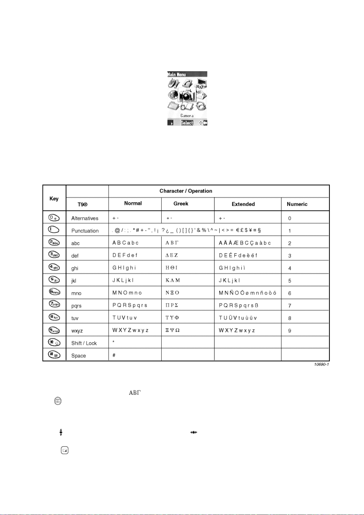
3.4. Alpha Entry
3.4.1 Character Set / Key Assignments
Alpha entry is used to enter alphanumeric characters in to the Phonebook, Short Messages and Greeting Message areas
Each time a key is pressed, it will display the next character. When another key is pressed, or no key is pressed for a short
time, the cursor will move to the next position.
To cycle between Greek characters ( ), extended characters ( A Ä Å ), numerals ( 0-9 ) and normal characters ( A B C
) press.
3.4.2 Editing Alpha Entry
Pressing will move the cursor up or down one line. Pressing will move the cursor left or right one character. When the
cursor is moved over a character and another key pressed this will insert the new character.
Pressing will delete the character to the left of the cursor.
PMCD030901C8 Section 3 Issue 1
OPERATING INSTRUCTIONS
3.5. Features Menu Structure
1. Settings
2. Contact List
3. Games / STK
4. Browser
5. Camera
6. Messaging
7.Data Folders
Display
Alerts
Keys
Phone Settings
Clock
Call Service
Call Divert
Security
Network
Defaults
Game 1 *
Game 2 *
News
Instructions
Settings
Home Page
Bookmark
Enter URL
Page Memo
Push Message
Browser Settings
Server List
Cookie
Last Status
Settings
Inbox
Broadcasts
Voice Mail
Create
e-mail
Data Folders
Outbox
SMS Chat
My Pictures
My Sounds
My Themes
User 1 **
User 2 **
User 3 **
User 4 **
User 5 **
Phone Lock
Call Bar
PIN1
PIN2
Fixed Dial
Barred Dial
MMS
SMS
email
Enable
Disable
MMS
SMS
email
Language
DTMF Length
All Tones
Active Flip
Warning Tones
Camera Tones
User Messages
Browse
Create
Voice Dial
Groups
Settings
SIM
Storage
Colour Priority
Font Size
Arrange Colour
Browser Images
Bookmarks
Push Reception
Receive
Message List
Topics
Languages
Ring Volume
Ring Type
Quiet Mode
Vibration Alert
Melody Composer
Voice Recorder
Auto Answer
Sort By
Search By
Separator
Hot Key Dialling
Voice Dial
MMS
SMS
email
Create
Edit
Family
Friends
Business
Useful
VIPs
User1
User2
User3
User4
Wallpaper
On/Off Show
Brightness
Backlight Time
Key Baclight
Clock/Calendar
Case Screen
MMS
SMS
email
8. Organiser
9. Connect
10732-1
Synchronization
Contacts List
Converter
Business Card
Schedule
Calculator
Alarm
Memo
Receive Object
Bluetooth
Infrared Dialup
Receive Object
View
Bluetooth
Infrared
Data Receive
Dial-Up
Record
Playback
Delete
Sync Schedule
Sync Contacts
Server List
Restore Schedule
Restore Contacts
Feature is SIM / Network / 3rd Party Service dependent.
*
User defined.
**
Figure 3.4: Features Menu Structure
Issue 1 Section 3 PMCD030901C8
Revision 0 – 6 – Service Manual
OPERATING INSTRUCTIONS
3.6. IMEI and Software Identification
To check the IMEI number of the phone:
Press: * # 0 6 #
To identify the software version installed on the phone:
Press: * # 9 9 9 9 # within five seconds of switching on.
3.7. SIM Personalisation
3.7.1 Introduction
SIM personalisation will limit the use of the telephone to a single SIM, a SIM supplied by one Network / Sub-network / Service
Provider or a SIM purchased by a company (corporation). If a personalised handset contains a SIM that is from a different
source, it will display the message “SIM ERROR” when switched on. This personalisation is sometimes referred to as SIM
lock or SIM latch.
3.7.2 Testing
To test a personalised handset when the user has not supplied the SIM, a SIM configured for test purposes (e.g. test SIM or
soft SIM) should be used. The mobile will recognise that the SIM is for testing purposes only and operate as normal.
3.7.3 Personalisation Function
Personalisation is activated during manufacture. Enabling / disabling is available by entering a special key sequence
immediately after power on. Once the enable / disable menu is shown it is possible to select the type of personalisation. When
personalisation is enabled it is only possible to disable it if the mobile contains a SIM and the 8 or 16 digit Control Key (CK) is
known. For security reasons, when CK is enabled, it cannot be read by the user.
There are two special key sequences to enter the enable / disable menu:
Key Sequence
4
7
5
2
6
8
24
Notes
Can only disable personalisation
Can both enable and disable personalisation
3.7.4 Disabling Procedure
1. Press
2. Scroll up / down
"SIM" for SIM Personalisation
"Network" for Network Personalisation
"Sub-Network" for Sub-Network Personalisation
"ServiceProvider" for Service Provider Personalisation, or
"Corporate" for Company Personalisation.
74
6
to select:
52
or
8
24
3. Press
4. Enter the 8 or 16 digit Control Key and press
5. Confirm by entering the 8 or 16 digit Control Key again and press
The display will confirm which type of Personalisation has been disabled.
PMCD030901C8 Section 3 Issue 1
Service Manual – 7 – Revision 0

OPERATING INSTRUCTIONS
3.7.5 Enabling Procedure
1. Press
2. Scroll up / down
"SIM" for SIM Personalisation
"Network" for Network Personalisation
"Sub-Network" for Sub-Network Personalisation
"ServiceProvider" for Service Provider Personalisation, or
"Corporate" for Company Personalisation.
3. Press
4. Enter the 8 or 16 digit Control Key and press
5. Confirm by entering the 8 or 16 digit Control Key again and press
The display will confirm which type of Personalisation has been enabled.
52
8
to select:
2
4
Issue 1 Section 3 PMCD030901C8
Revision 0 – 8 – Service Manual

TECHNICAL DESCRIPTION
4 TECHNICAL DESCRIPTION
4.1. RF Overview
4.1.1 General Specifications
The telephone is a triple band product incorporating three switchable transceivers, EGSM 900 band,GSM 1800 (DCS 1800)
band and GSM 1900 band. The transmit and receive bands are given in the table below:
Tx Rx
EGSM 900 880-915 MHz 925-960 MHz
GSM 1800 1710-1785 MHz 1805-1880 MHz
GSM 1900 1850-1910MHz 1910-1990MHz
Other notable technical features are as follows:
EGSM 900 GSM 1800 GSM 1900
Rx Bandwidth 35 MHz 75 MHz 60MHz
Tx Bandwidth 35 MHz 75 MHz 60MHz
Duplex Spacing 45 MHz 95 MHz 80MHz
Number of Channels 174 374 299
ARFCN (Channel Numbers) 975 - 1023 512 - 885 512 - 810
0 - 124
1st Tx Channel 880.2 MHz 1710.2 MHz 1850.2MHz
(Ch 975) (Ch 512) (Ch 512)
Last Tx Channel 914.8 MHz 1784.8 MHz 1909.8MHz
(Ch 124) (Ch 885) (Ch 885)
1st Rx Channel 925.2 MHz 1805.2 MHz 1930.2MHz
(Ch 975) (Ch 512) (Ch 512)
Last Rx Channel 959.8 MHz 1879.8 MHz 1989.8MHz
(Ch 124) (Ch 885) (Ch 885)
Maximum Tx Power 33.0 dBm 30.0 dBm 30.0 dBm
(Class 4) (PL5) (Class 1) (PL0) (Class 1)
Minimum Tx Power 5.0 dBm 0.0 dBm 0.0 dBm
(PL19) (PL15) (PL15)
4.1.2 Description of PCBs
The handset is of clam-shell design and uses two printed circuit boards (PCBs).
The Main PCB is constructed of eight-layer FR4 material. All RF components are located on one side of the top half area of
the Main PCB, with the baseband components (Logic circuits) occupying the lower half of the Main PCB. The RF circuit area
is shielded by two metal screens. The Logic and Bluetooth circuits are shielded by one screen each.
The keypad is mounted on the reverse side of the Main PCB.
The second PCB is of flexible printed circuit type. All components and the connectors for the Sub LCD module, camera,
receiver, main display (x2) are located on one side of this assembly.
PMCD030901C8 Section 4 Issue 1
Service Manual – 9 – Revision 0
TECHNICAL DESCRIPTION
1
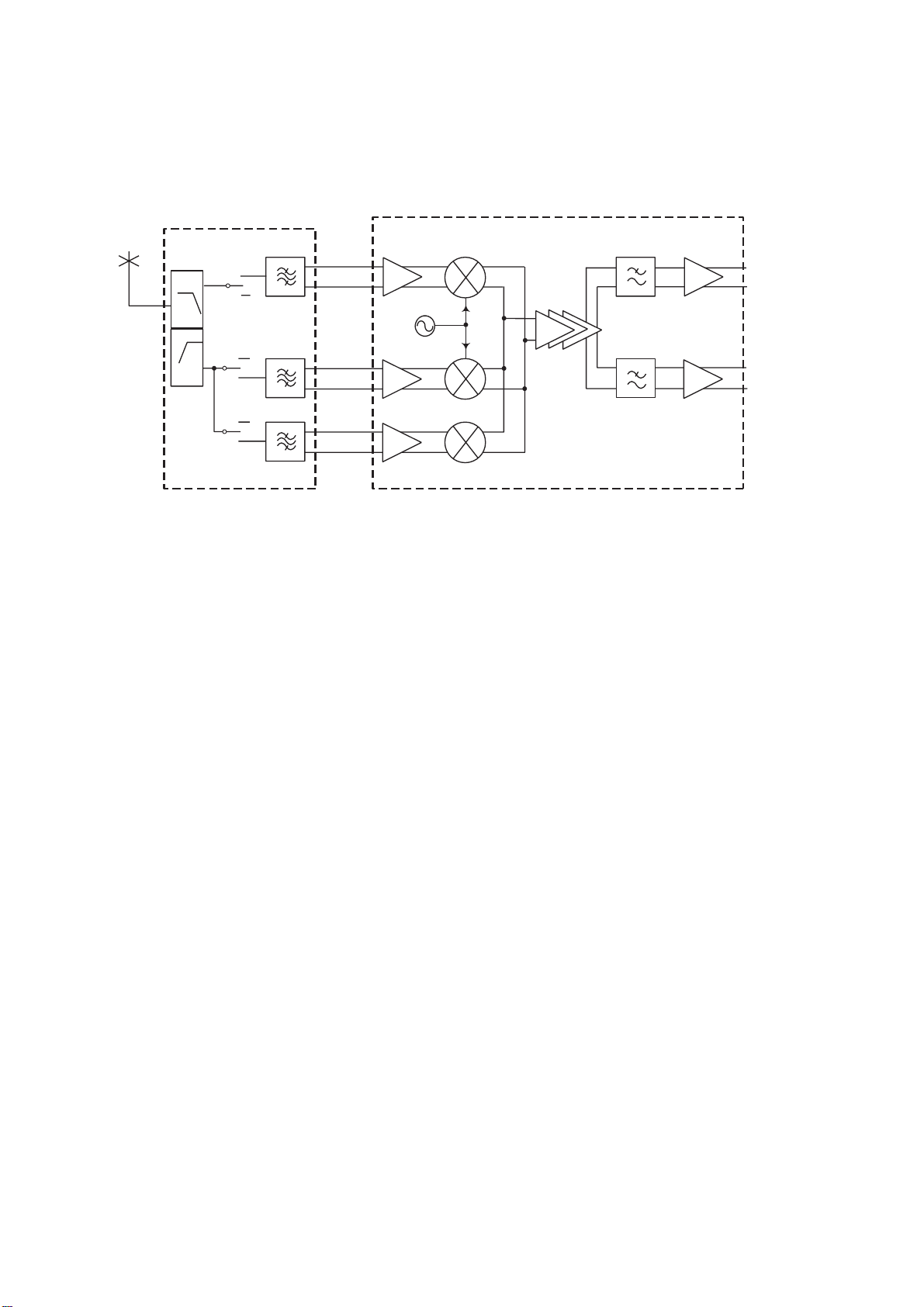
4.1.3. Block Diagram
FRONT END
(SWITCH MODULE)
LPF
Rx
Tx
Tx
HPF
Rx
Tx
Rx
COUPLER
COUPLER
EGSM 900
GSM 1800
GSM 1900
TRIPLE
BAND
PA
TRIPLE BAND TRANSCEIVER
EGSM 900
ATTENUATORS
GSM 1800 / 1900
LNA
LNA
LNA
RF
LO
BUFFER AMP
PGC
AMP
900
1800 /
1900
BASEBAND
FILTERS
÷4
÷2
BASEBAND
AMPLIFIERS
RF
VCO
IR
IRX
QR
QRX
I
Q
I
Q
10699-1
4.1.4. Frequency Plan
E-GSM 900
I, Q output
Rx: 925 - 960 MHz
RFLO VCO
1/4
3520 - 3840 MHz
Tx: 880 - 915 MHz
to baseband
925 - 960 MHz
880 - 915 MHz
I, Q output from
baseband
4.1.5 Synthesiser
APC
Figure 4.1: RF Block Diagram
Rx: 1805 - 1880 MHz
RFLO VCO
3420 - 3760 MHz
Tx: 1710 - 1785 MHz
Figure 4.2: Frequency Plan
PA RAMP
GSM 1800
1/2
I, Q output
to baseband
1805 - 1880 MHz
1710 - 1785 MHz
I, Q output from
baseband
Rx: 1930 - 1990 MHz
RFLO VCO
1/2
3700 - 3980 MHz
Tx: 1850 - 1910 MHz
GSM 1900
I, Q output
to baseband
1930 - 1990 MHz
1850 - 1910 MHz
I, Q output from
baseband
10655-
Transceiver IC U603 has a synthesiser and VCO for generating appropriate signals for the transmitter and receiver. Channel
data is transferred to IC603 from the baseband IC by three-wire bus (Data, Clock and Strobe). Signal output is divided by 4 for
EGSM 900 and by 2 for GSM 1800 / GSM 1900. Synthesiser lock time is approximately 180 µs.
An external TCXO is used to generate a 26 MHz reference signal for the transceiver and logic block. AFC is employed to
maintain stability over changes in temperature.
Issue 1 Section 4 PMCD030901C8
Revision 0 – 10 – Service Manual
TECHNICAL DESCRIPTION
4.1.6. Antenna
The antenna is a fixed helical type and is designed for triple band operation (EGSM 900, GSM 1800 and GSM 1900).
4.2. Transmitter
4.2.1 Functional Description
U603
RF
VCO
÷4
I
Q
I
Q
TRIPLE BAND
TRANSCEIVER (PART)
900
÷2
1800 /
1900
FL605
FL606
U604
BUFFER AMP
FL608
SAW
ATTENUATOR
FILTER
EGSM 900
GSM 1800 / 1900
x2
PA RAMP
U601
TRIPLE BAND
PA
U605
APC
U609
U607
FL600
SWITCH
MODULE
900
1800 /
1900
ANTENNA
RF TP /
SWITCH
10697-1
Figure 4.3: Transmitter Block Diagram
The transceiver IC (U603) supports quadrature modulation and employs direct modulation. The I, Q signal provided from the
baseband circuits is up-converted to the transmit frequency by this modulator. The required signal path is selected
(EGSM 900 or GSM 1800 / GSM 1900). The signal level is approximately 0 dBm.
The modulated output is fed into the pre-amplifier U604 via SiCu filters FL605 and FL606. The filters suppress third order
harmonics of the modulated signals. Pre-amplifier U604 is a quad band limiter amplifier whose output signal is applied to the
dual input of the triple band power amplifier U601 via Pi attenuators. The Pi attenuators provide a better return loss and
correct input levels for U601. A 3-port EGSM SAW filter FL608 is employed at the EGSM 900 output of U604 to provide extra
filtering of transmitter noise at the bottom edge of the EGSM 900 and GSM 900 bands repectively. FL608 also acts as a balun
between the balanced output of U604 and the unbalanced input of U601.
Filtering of transmitter harmonics, most of which are from the PA, is provided by couplers U609 (EGSM 900) and U607
(GSM 1800 / GSM1900). The output from the couplers is applied to the antenna switch (front end module) FL600 which
provides a connection path via the RF test point to the external antenna.
The coupled outputs are combined at the input of U605, an Automatic Power Control (APC) IC, to control the gain and output
power of the PA. An RF detector in U605 produces a baseband output which is compared with a control signal from the logic
section to produce a control signal for the PA.
PMCD030901C8 Section 4 Issue 1
Service Manual – 11 – Revision 0
TECHNICAL DESCRIPTION
4.3. Receiver
4.3.1 Functional Description
10698-1
LPF
HPF
FL600
SWITCH
MODULE
Rx
Tx
Tx
Rx
Tx
Rx
EGSM 900
GSM 1800
GSM 1900
LNA
RF
LO
LNA
LNA
TRIPLE BAND TRANSCEIVER
U603
PGC
AMP
BASEBAND
FILTERS
BASEBAND
AMPLIFIERS
IR
IRX
QR
QRX
Figure 4.4: Receiver Block Diagram
The main building block for the receiver is the transceiver IC (U605) which includes a direct conversion receiver with I and Q
quadrature demodulation.
Received signals from the antenna are passed via the RF to the antenna switch module (front end module) FL600. This
module contains a diplexer which filters the signal to the required receiver path (EGSM 900 or GSM 1800 / GSM 1900). Pin
diode switches within FL600 route the signal path from the transmitter or to the receiver as required.
Internal SAW filters in FL600 provide attenuation of signals outside the required receive band which could degrade the signalto-noise ratio of wanted signals. There is a SAW filter for each of three receiver bands, EGSM 900, GSM 1800 and
GSM 1900.
The received signal is output to the port of FL600 and carried by a balanced pair of printed circuit tracks to the corresponding
frequency band LNA input of transceiver U603. Output from the LNA is then converted directly to baseband frequency by a
quadrature demodulator mixer.
The local oscillator (LO) signal presented to the mixer is provided by an internal VCO and is divided by 4 (EGSM 900) or by 2
(GSM 1800 and GSM 1900).
At baseband, the GSM signal is passed through a 1-pole blocking filter (comprising two external capacitors) and a channel
filter. These filters provide some attenuation to adjacent channel signals at the receiver input. An equaliser stage in the
baseband IC is used to correct any group delay variation which causes distortion of the received signal.
The baseband signal is then amplified by programmable variable gain amplifier (PGA) stages within U603. Combined with the
LNA these give a total gain between -2 dB and +85 dB.
The I and Q baseband signals are then offset to a DC offset level produced by U603 to 1.35 V. this offset level provides the
largest dynamic range available for the receiver, which is limited by SYREN baseband IC. SYREN provides analogue to digital
conversion of the demodulated signal and also some further 45dB attenuation to adjacent channel interference through DSP
filtering.
Issue 1 Section 4 PMCD030901C8
Revision 0 – 12 – Service Manual
Service Manual
– 13 –
Revision 0
4.4. Baseband Overview
4.4.1 Introduction
The Baseband circuits of the phone are required to perform the following functions:
• Equalisation
• Channel coding / decoding
• Speech coding / decoding
• Data Encryption
• Layer 1, 2 and 3 software tasks
• Man Machine interface (MMI)
• System Interface
• SIM Interface and Management
• Audio and Tone Generation
• Power supply and battery management
• RF power control
• Synchronisation
• Real time clock
TECHNICAL DESCRIPTION
Figure 4.5: Baseband Block Diagram
PMCD030901C8 Section 4 Issue 1
TECHNICAL DESCRIPTION
The Baseband circuits are built around a GSM chipset developed by Texas Instruments. The chipset comprises two chips,
CALYPSO+ and SYREN. The highly integrated nature of the chips means that each contain a large number of functions.
CALYPSO+ is a signal processing device with a digital signalling processor (DSP) and CPU. The DSP performs channel and
speech encoder/decoder tasks, together with equalisation and encryption. The CPU runs layer 1, 2, and 3 software, controls
the MMI, SIM and system interfaces, real time clock, and battery and power management. CALYPSO+ also controls SYREN.
SYREN provides frame timing, A/D conversion, RF power control, audio interfacing including tone generation, and baseband
power supplies.
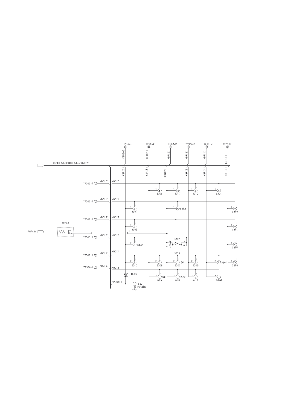
4.4.2 Keypad
The keyboard interface supports keypads up to 6 columns by 6 rows and has a built-in scanning algorithm for hardwarebased key press decoding. Four key press detection modes are offered: matrix, allowing 25 keys to be scanned. When a key
being pressed, a keypad interrupt is generated. To find which key has been pressed, the software scans each column in turn
and reads which row is active. Because of key bounce, the key press is confirmed twice at approximately 20 ms intervals.
• Event detection on both key press and key release.
• Programmable press detection on key release only.
• Long key detection on prolonged key press.
• Time out on permanent key press or after keyboard release.
10689-1
Figure 4.6: Keypad Connections
The controller supports detection of single and multiple key presses. On a key press or key release, and allowing for
debounce time, the scanning sequencer is activated. The resulting digital snapshot of the keypad is registered and compared
to the previous one. On change detection, an interrupt is sent to the MCU.
Issue 1 Section 4 PMCD030901C8
Revision 0 – 14 – Service Manual
TECHNICAL DESCRIPTION
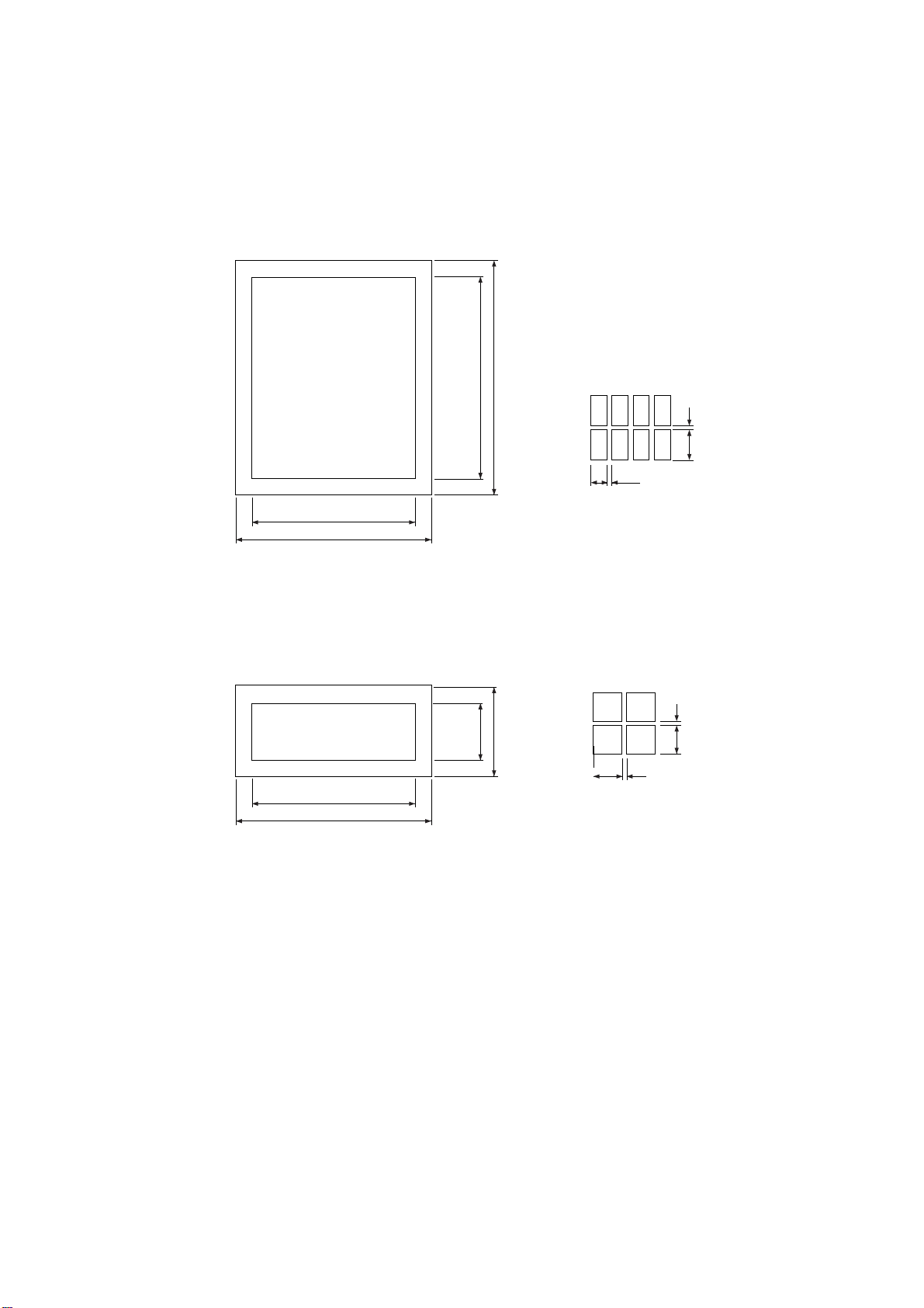
4.4.3 LCD Modules
The handset has two displays forming a single module. The main display is positioned inside the clamshell of the handset
while the sub display is mounted on the outside of the top half of the handset.
The Main LCD module consists of a Transmissive TFT colour display driven by a chip-on-glass driver connected to the LCD /
Camera interface.
The display has 132 x 176 pixels which can be used to display chinese characters in addition to different font sizes.
The display driver has its own internal display RAM.
View Area
Effective Area
All dimensions are in
millimetres (mm)
132 x 176 Pixels
(X70)
38.016
42.2
RRGGBBR
0.01
0.206
R
0.071
28.512
33.6
0.01
10691-1
Figure 4.7: Main LCD Dimensions
The Sub-LCD module is a passive Film SuperTwist Nematic (FSTN) monochrome display which is physically part of the main
display module but has its own chip-on-glass driver IC. This driver is connected to the CALYPSO+ microwire interlace.
96 x 28 Pixels
(X70)
View Area
Effective Area
19.2
25.6
5.6
10.5
All dimensions are in
millimetres (mm)
0.015
0.185
0.015
0.185
10693-1
Figure 4.8: Sub-LCD Dimensions
4.4.4 Camera Module
The camera module is a CMOS CIF sensor type. It is connected to the CALYPSO+ device via an interface IC and provides
output in RGB565 format.
Automatic Light Control (ALC) and Auto White Balance (AWB) is built in to the camera module.
4.4.5 Interface IC
The ROHM Interface IC is used to control communication between the CALYPSO+ IC and:
• Main LCD
• Camera module
It is also used to provide PWM brightness control for the red, green or blue backlight for the sub-LCD, and PWM brightness
control for the photo-light.
PMCD030901C8 Section 4 Issue 1
Service Manual – 15 – Revision 0

TECHNICAL DESCRIPTION
4.4.6. Infrared Transceiver
The Infrared transceiver is a 115 kbits/s IrDA transceiver with a transmission range of approximately 20 cm. The transceiver is
connected directly to CALYPSO+ via RX, TX and shutdown (SD) data lines.
4.5. CALYPSO+
4.5.1 Introduction
CALYPSO+ contains the DSP, CPU, GSM timing and peripheral functions. The software for DSP is contained in masked
ROM.
4.5.2. Subscriber Identity Module (SIM)
The SIM interface is designed to support 3 V SIMs.
4.5.3 TPU
The TPU provides the GSM TPU TDMA timing requirements for the system.
The TPU parallel outputs are as follows:
TPU Timing output signal assignments of CALYPSO+
Name Ball No. Function Connection Configuration
TSPACT 0 V10 PAON External
TSPACT 1 V11 PLLON RF
TSPACT 2 V12 N/C
TSPACT 3 R12 TX_ON1 RF
TSPACT 4 P12 N/C
TSPACT 5 W13 N/C
TSPACT 6 AA13 DCS_PAON RF
TSPACT 7 V13 GSM_PAON RF
TSPACT 8 V14 N/C
TSPACT 9 R13 N/C
TSPACT 10 P13 N/C
TSPACT 11 W15 N/C
The timed serial port is used to control the SYREN device and the PLL of the RF section. It can be controlled either by the
CPU or by the TPU. The serial ports are as follows:
Timing serial port assignments of CALYPSO+
Name Ball No. Function Connection Configuration
TSPEN 0 V15 nTSPEN SYREN
TSPEN 1 Y17 N/C
TSPEN 2 AA17 PLL_STRB RF
TSPEN 3 V16 N/C N/A
TSPEN 4 W17 N/C
TSPCLKX V14 PLL_CLK RF
TSPDI Y16 N/C
TSPDO W16 PLL_SD/TDR RF
The MCU controls the TPU through a double-page memory buffer, the TPU Communication buffer. Only one page is
accessible by the MCU at any time. Page selection is handled by TPU. The size of each page is 256 x 16.
Issue 1 Section 4 PMCD030901C8
Revision 0 – 16 – Service Manual

TECHNICAL DESCRIPTION
4.5.4 CPU Memory
The phone uses the following memory configuration:
• 256 Mbits Flash memory
• 5 Mbits internal SRAM
• 128 Mbits external PSRAM
Although CALYPSO+ has 5 Mbits internal memory, only the external PSRAM memory is protected by the backup battery.
4.5.5 Real Time Clock (RTC)
Clock functions are provided by a Real Time Clock built into CALYPSO+. The module is synchronised by a 32.768 kHz crystal
and is powered via a dedicated regulator in SYREN and is backed up by a 2.5 V cell.
CALYPSO+ has a clock auto compensation function to take into account any inaccuracies of the crystal. It is able to calibrate
crystal tolerance / drift by writing to the compensation registers. This calibration can adjust the clock to a resolution of
1 x 32768 Hz clock period.
Registers for RTC are assigned between $FFFE:1800 - $FFFE:1814.
4.5.6 Timers
There is a watchdog timer and two 16 bit general-purpose timers which can be used either as auto reload or one-shot timers
to provide interrupts to the ARM CPU. The watchdog timer receives a 928 kHz clock signal from the CALYPSO+ clock
module. A combination of pre-scaler and timer register gives a timeout range of 1.078 s to 9.039 s.
The general purpose timers receive a 812.5 kHz clock signal.
4.5.7 UART
CALYPSO+ has three UART ports, MODEM_1, MODEM_2 and UART / IrDA. The MODEM_1 port is used for data
connection, MODEM_2 for interfacing to the Bluetooth IC and UART / IrDA for modem port is used for IrDA data
transmissions.
UART / MODEM PORT ASSIGNMENT
CALYPSO+ SIGNAL Ball No. FUNCTION I/O
TX_Modem_1 A20 UART serial data TX (SERIAL_DN) O
RX_Modem_1 C18 UART serial data RX (SERIAL_UP) I
CTS_Modem_1 D17 UART Clear to Send (CTS) I
RTS_Modem_1 D16 UART Request to Send (RTS) O
DSR_Modem_1 B19 UART Data Set Ready (DSR) I
TX_Modem_2 D12 Bluetooth TX Data O
RX_Modem_2 B13 Bluetooth RX Data I
CTS_Modem_2 G12 Bluetooth Clear to Send I
RTS_Modem_2 G13 Bluetooth Ready to Send O
TX_IRDA A18 UART serial data TX (reserved) O
RX_IRDA C17 UART serial data RX (reserved) I
TXIR_IRDA C16 IrDA serial TX data in SIR mode O
RXIR_IRDA B18 IrDA serial RX data in SIR mode I
SD_IRDA D15 IrDA module shutdown (high = shutdown) O
Registers for the UARTs are located from $FFFF:5000 to $FFFF:5011 (UART / IrDA), $FFFF:5800 to $FFFF:5811
(MODEM_1) and from $FFFF:6000 to $FFFF:6011 (MODEM_2).
PMCD030901C8 Section 4 Issue 1
Service Manual – 17 – Revision 0
TECHNICAL DESCRIPTION
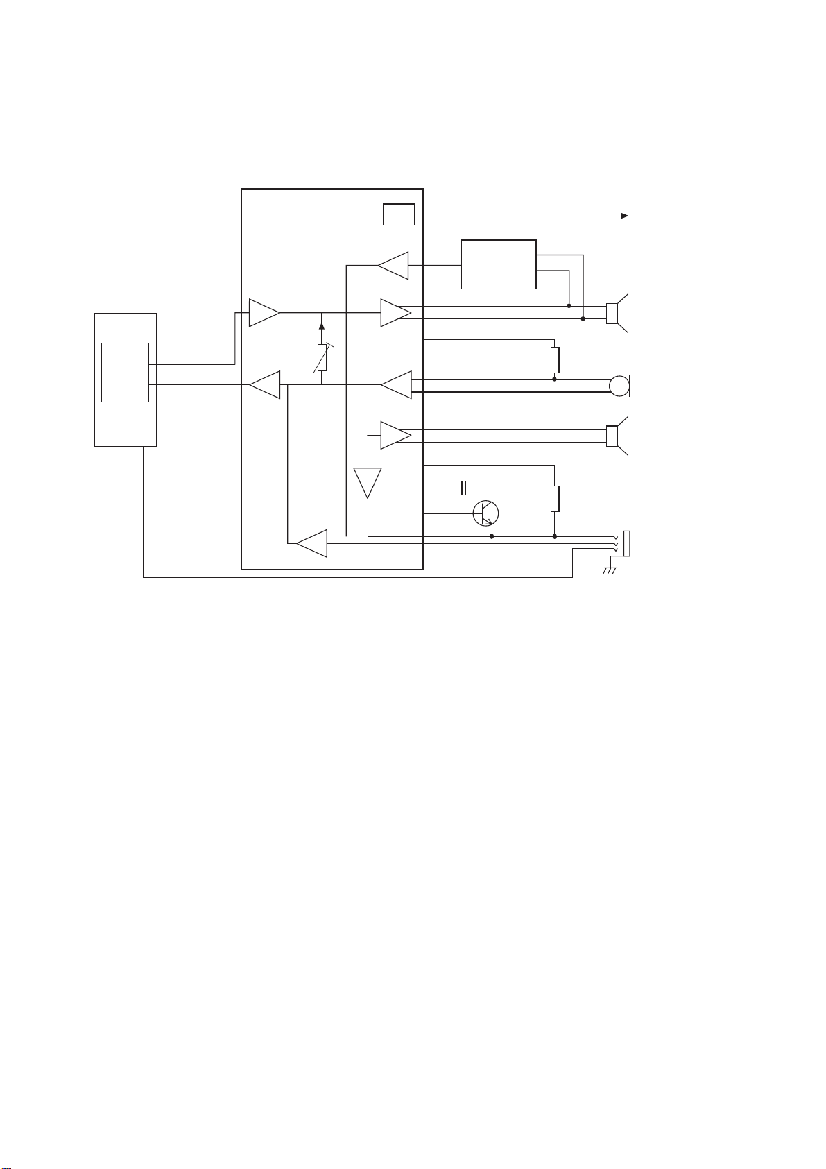
4.6. SYREN
4.6.1 Introduction
SYREN U120 contains the interace circuits to the audio, RF and auxiliary analogue functions. It is configured using the TSP
on CALYPSO+ and interfaces with the DSP in CALYPSO+ via the voice and I & Q interfaces.
CALYPSO
10694-1
U100
DSP
VOICEBAND I/F
nPHF±DET
U120
SYREN
SIDETONE
APC
Figure 4.9: SYREN Device U120
PARAMP
HSO
HSVMID
APC (U605)
U301
MELODY
GENERATOR
DTHF SPEAKER
MICBIAS
MICROPHONE
RECEIVER
HSMICBIAS
TR402
PERSONAL
HANDSFREE
(PHF)
nPHF±DET
4.6.2 Power Amplifier Ramp (APC)
The purpose of the Automatic Power Control is to generate an envelope signal to control the power ramping up, ramping
down and power level of the radio burst.
It includes a DAC and RAM in which the shape of the envelope (ramp-up and ramp-down) are stored digitally. The envelope
signal is converted to analogue by a 10-bit DAC. RF requirements determine the co-efficient of the ramp shape.
Timing of the APC is generated internally and is dependent on real time signals from TSP and the content of two registers
which control the relative position of the envelope signal versus the modulated I & Q.
4.6.3 Audio
SYREN provides the analogue interface for the digital audio samples processed by the DSP in CALYPSO+. A 16mm 8 Ω
speaker mounted on the back of the handset is used both for playing ring tones and for desktop handsfree (DTHF) functions.
The personal handsfree (PHF) headset connects directly to the HSO (earpiece) and HSMIC (microphone) pins of the SYREN
device. Bias for the microphone is provided by HSMICBIAS from SYREN. Detection of PHF connection is made by an
interrupt on IO(2) of CALYPSO+. A small delay is applied before HSOVMID bias voltage is activated to minimise noise heard
in the headset when HSO is enabled. This voltage controls transistor TR402 which delays the bias at the headset connector.
Melodies and simple ring tones are produced by Melody Generator U301 which outputs these to both the DTHF speaker and
to AUX1 of SYREN. The audio feed to SYREN allows ring tones and melodies to be played at a lower level through the PHF
headset. U301 is controlled via the CALYPSO+ microwire interface with an interrupt signal to indicate when its FIFO buffers
are empty.
4.6.4 LED Driver
SYREN contains an open collector type output for the Charge LED control. The default state is ON to enable indication of
charging in the case of a deeply discharged battery.
Issue 1 Section 4 PMCD030901C8
Revision 0 – 18 – Service Manual
TECHNICAL DESCRIPTION
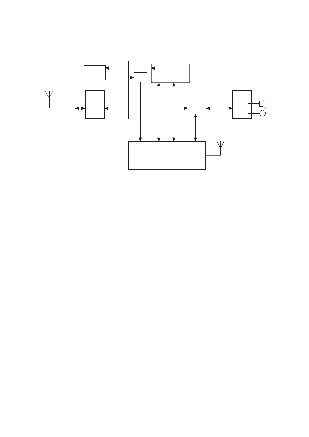
4.7. Bluetooth Module
Bluetooth module U500 provides short range (typically 10 metres or less) connectivity from the handset to Bluetooth-enabled
devices such as headsets, car kits, personal computers for transferring voice and data.
VCXO_EN
VCXO
26 MHz
÷2
CPU
10695-1
GSM
RF
U120
SYREN
(PART)
ADC
BASEBAND
13 MHz
GPIO
CLK
REQ
U500
BLUETOOTH
MODULE
CALYPSO+
MODEM-2
UART
U100
DSP
PCM AUDIO
VOICEBAND
MCSI-2
U120
SYREN
(PART)
DAC
Figure 4.10: Bluetooth Module
The Bluetooth module connects to the MODEM-2 UART in CALYPSO+ which provides the control and data interface to the
baseband CPU. The 4-wire UART connection (TXD, RXD, RTS, CTS) uses the HCI(H5) protocol with error detection and retransmission.
A PCM audio connection from U500 connects via the CALYPSO+ MCSI-2 port to the DSP. This connection is 4-wire and uses
13-bit linear PCM. The DSP switches audio to the baseband interface (Bluetooth headset mode) or to the voiceband interface
(Bluetooth cordless mode).
In standby mode, U500 runs from its internal slow speed clock. In active mode, U500 runs off a 13 MHz clock derived from the
VCXO. To enable the 13 MHz clock, U500 asserts CLK_REQ which will interrupt CALYPSO+ to enable the VCXO. U500 is
powered from SYREN 2.8 V regulator VMEM and derives 1.8 V from this source to power its RF circuits. VRIO powers the
baseband I/O interface voltage rails.
U500 resets itself at switch on. Additionally, a CALYPSO+ GPIO connects to RST_B to allow software control of Bluetooth
resetting. Under normal conditions, CALYPSO+ holds U500 in reset until its power rails and the 13 MHz clock have been
enabled.
The 6-byte Bluetooth Address is contained in the Retained Data Store (RDS) which is programmed during manufacture. It is
loaded into U500 at power on.
PMCD030901C8 Section 4 Issue 1
Service Manual – 19 – Revision 0
TECHNICAL DESCRIPTION
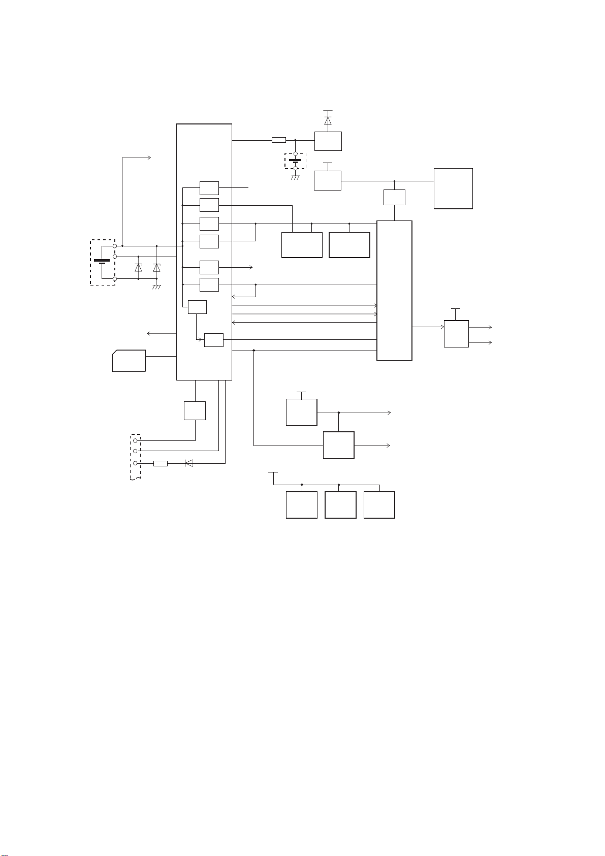
4.8. Power Supplies
4.8.1 Introduction
U120
SYREN
VBAT
MAIN
BATTERY
BAT-TEMP
UPR
MICBIAS
MIC
CN300
(SIM)
VRSIM
VR
VR
VR
VR
VR
VR
EXT-IRQ
VR
VBACKUP
VRRAM
VRMEM
VRIO1
VRIO2
VRABB
A28BB
VRDBB
VSDBB
VRRTC
BACKUP
CELL
D28V
U500
BLUETOOTH
VBAT
U142
REG
VBAT
U141
REG
GENERATOR
D18V
D28VB
U301
MELODY
ONOFF
RESPWONZ
D15RTC
ONNOFFONNOFF
D15V
Q202
U100
CALYPSO
INT2
D18VMEM
RF_EN
U140
FLASH
+ SRAM
VBAT
U602
REG
VSTX
VSRF
ACC±PWR±EN
Q400
I/O
CN2702
ACC±PWR±IO
EXTPWR
nACC-SENSE
VBAT
Figure 4.11: Power Supply Block Diagram
The Power Management Block consists of six parts as follows:
1. Power Source
2. Power On/Off Control
3. Power Source Failure detection
4. Voltage Regulation
5. Battery Charging & Monitoring
6. Accessory Control
4.8.2 Power Source
VBAT
U141
REG
ONNOFF
KEYPAD
BACK-
LIGHTS
TR201 /
TR202
SW
LCD
BACK-
LIGHTS
D18V
D18VMEM
CAMERA
10696-1
The battery comprises a single Lithium-Ion (Li-Ion) cell with a nominal voltage of 3.7 V and 680 mAh capacity. This type of
battery has an advantage in weight and size over Nickel Metal Hydride (NiMH) cells.
Issue 1 Section 4 PMCD030901C8
Revision 0 – 20 – Service Manual

TECHNICAL DESCRIPTION
4.8.3 Power On / Off Control
The power on sequence can begin when VBAT >2.6 V or VBACKUP >2.6 V. In this state SYREN (U120) is in Power On
Condition and internal supply UPR is active. RESPWRONZ signal to CALYPSO+ (U100) is released high.
If SYREN is in the Power On Condition, one of following conditions start the Power Up sequence.
• Power key is pushed for more than 30 ms.
• EXTPWR voltage is higher than (VBAT+0.4) V.
• CALYPSO+ RTC ALARM signal goes high.
The Power Up sequence is as follows:
1. SYREN internal band gap reference is activated.
2. If VBAT < 3.2 V after a timeout of 51.2 ms Power Up sequence is aborted.
3. All regulators (VRDBB, VRMEM, VRRAM, VRIO & VRABB) are enabled.
4. Power Up status bit and internal Reset bits are set.
5. ONNOFF signal is set to activate CALYPSO+.
6. ARM in CALYPSO+ starts running software using 32 kHz clock, and also starts 26 MHz clock.
The following Power Down sequence can only be started by CALYPSO+ setting the DEVICE_OFF bit in SYREN or, in
emergency case, when VBAT < 2.7 V (or VBAT < Vbackup & VBAT < 2.8 V):
1. If emergency case, INT1 is set low by SYREN.
2. SYREN starts an internal 150 µs watchdog timer to allow CALYPSO+ to shutdown.
3. ONNOFF signal is reset to deactivate CALYPSO+.
4. All regulators (VRDBB, VRMEM, VRRAM, VRIO, VRABB & VRRAM) are disabled.
5. SYREN internal band gap reference is deactivated.
4.8.4 Power Source Detection Failure
If the power fails (i.e. battery removal) the software detects INT1 and asserts the MODE pin of the PSRAM low to back up the
contents.
4.8.5 Voltage Regulation
The voltage regulators for I/O and memories have a nominal output of 2.8 V, and are designed to provide a minimum 2.7 V
output over all load, transients and temperature conditions.
Each power source is specified as follows.
• D15V: (SYREN VRDBB) Power supply for the CALYPSO+ (Lead Mega Module) LMM block.
Voltage 1.5 V ±0.15 V
Current 170 mA max.
Dropout 100 mV max (load max)
Supply VBAT
This power supply provides the power for CALYPSO+ internal RAM, ASIC modules, LMM and ARM Blocks, and is
selectable from 1.3 V, 1.5 V and 1.8 V.
• D28VB: SYREN (VR10) Power supply for SYREN ASIC I/O and CALYPSO+ .
Voltage 2.8 V ±0.1 V
Current 100 mA max.
Dropout 100 mV max (load max)
Supply VBAT
This is the main power supply for the baseband digital sections (I/O and LCD) and some analogue sections. It is also used
for the digital I/O ring on both CALYPSO+ and SYREN.
PMCD030901C8 Section 4 Issue 1
Service Manual – 21 – Revision 0

TECHNICAL DESCRIPTION
• D18VMEM / D18V: Power supply used by Flash and PSRAM memory and memory I/O, vibrate.
Voltage 1.8 V ±0.1 V
Current 450 mA max.
Dropout 100 mV max (load max)
Supply VBAT
The D18V power supply is provided by a permanently enabled discrete 1.8V regulator IC. This rail is used to supply the
vibrate motor and is FET switched to provide the D18MEM rail for the CALYPSO+ memory interface and external flash
memory IC.
• D28V: (SYREN VRMEM) Power supply for the Bluetooth module.
Voltage 2.8 V ±0.1 V
Current 60 mA max.
Dropout 100 mV max (load max)
Supply VBAT
Supplies the Bluetooth module U500.
• VRRAM: not used.
Voltage 2.8 V ±0.1 V
Current 50 mA max.
Dropout 100 mV max (load max)
Supply VBAT
• VRABB: Digital Power supply for SYREN analogue section.
Voltage 2.8 V ±0.1 V
Current 80 mA max.
Dropout 100 mV max (load max)
Supply VBAT
This supply provides power for the internal SYREN analogue section.
• VRSIM: Digital Power supply for SIM card.
Voltage 2.15 V ±0.15 V
Current 10 mA max.
Dropout 100 mV max (load max)
Supply VBAT
Supplies power for the SIM card.
• VRRTC: Digital power supply for CALYPSO+ 32 kHz oscillator and RTC module (VRRTC).
Voltage 1.5V ±0.15V
Current 30
µA.
Dropout 100 mV max (load max)
Supply UPR
Supplies power for the CALYPSO+ 32 kHz oscillator and RTC module. Selectable from 1.3 V, 1.5 V and 1.8 V. It is
supplied from UPR to enable it to be maintained from the backup cell when the main battery is removed.
Issue 1 Section 4 PMCD030901C8
Revision 0 – 22 – Service Manual
TECHNICAL DESCRIPTION
• VRUSB: not used.
Voltage 3.3 V ±0.2 V
Current 15 mA max.
Dropout 100 mV max (load max)
Supply USB_VBUS (5V +0.5 V, -1 V
4.8.6 Regulator Sleep Function
To reduce power consumption in the analogue section of the baseband chipset, the voltage regulators can be placed in a low
power mode or disabled by the processor when it enters a low activity sleep mode. During sleep mode, VRABB, and VRDBB,
VRIO, VRMEM, VRRAM and VRSIM are switched to low power mode.
4.8.7 Battery Charging and Monitoring
The status of the LCD battery icon is determined by the value of BAT_VOLT returned from the SYREN MADC, as indicated in
the table:
Icon Status Battery Capacity
3 bar 100% to 50% 3.77 V < 3.83 V <
2 bar 50% to 20% 3.68 V < < 3.77 V 3.74 V < < 3.83 V
1 bar 20% to 0% 3.40 V < < 3.68 V 3.46 V < < 3.74 V
Low Voltage Alarm 0% < 3.40 V < 3.46 V
Two types of external charging accessories are available for the handset - a switching type AC Adaptor and a DC Adaptor.
Battery charging is controlled by the CPU within the phone. If external power is detected and the temperature is within
specified limits, the charger starts the rapid charge algorithm. Battery charge termination for the Li-On battery is reached
when the charging current in constant voltage mode reaches 50 mA. Charging is aborted if the current is greater than 800 mA
or the battery voltage rises above 4.25 V.
Input Output
Voltage Voltage Current
AC Adaptor 100 - 240 V 5.8 V ±0.2 V 650 mA ± 100 mA
DC Adaptor 5.8 V ±0.2 V 700 mA ± 30 mA
Battery Voltage Battery Voltage
(In Call) (Standby)
Deeply-Discharged Batteries
In the case of deeply discharged batteries, there may not be enough power in the battery to initiate charging. In this case, the
charging circuit automatically starts to trickle charge the battery until there is enough power to switch on the phone. LED
indication will be provided to the user even though the handset is not active.
The LED will switch off when charging is complete. The time to reach the fast charge state is dependent on the trickle charge
current (approximately 46 mA at VBAT = 2.5 V) but is specified as less than 16 minutes worst case.
Over Voltage Protection
As the accessory connector is unique to Panasonic, only approved chargers can be used with the handset. Therefore, no
additional circuitry is required within the handset to prevent the charger voltage exceeding the design limit of 20 V.
PMCD030901C8 Section 4 Issue 1
Service Manual – 23 – Revision 0
 Loading...