

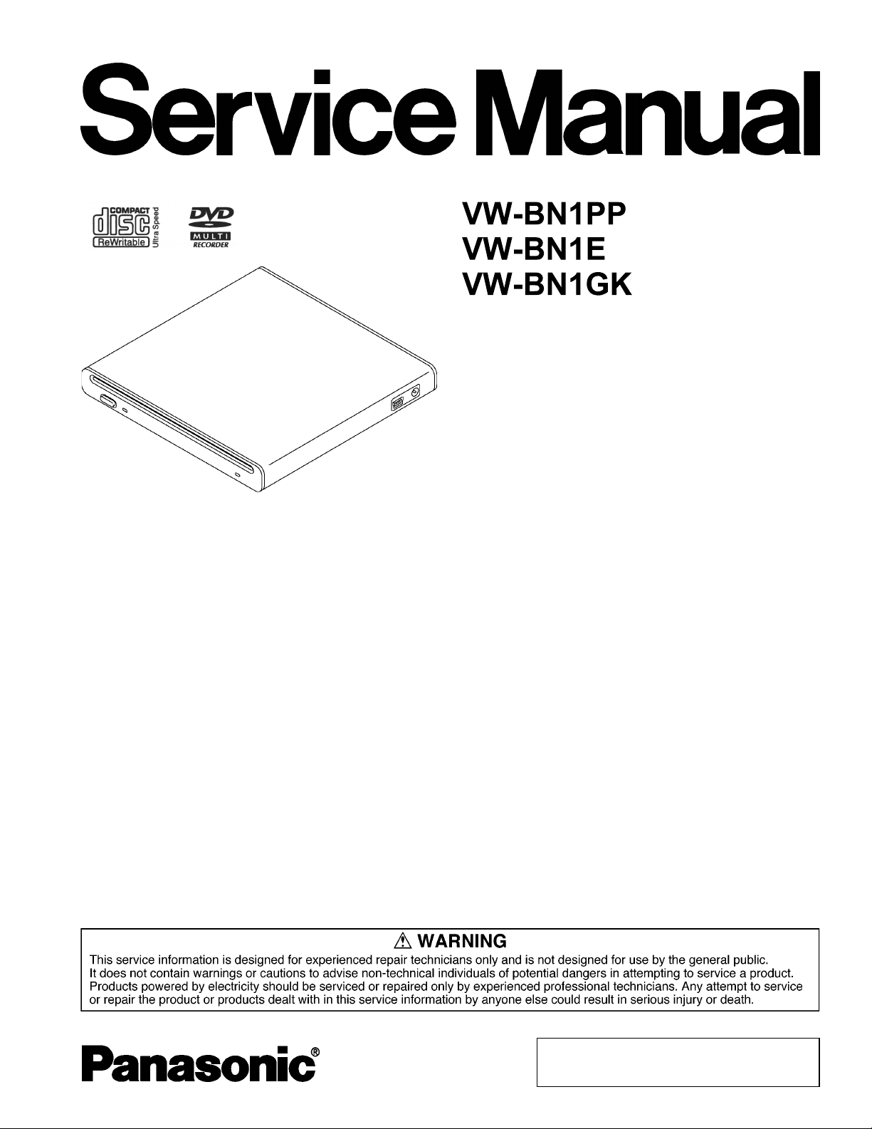
Panasonic VW-BN1E-GK-PP Service Manual
Colour
(S)....................Silver Type
ORDER NO.VO0708003CE
B27
DVD Burner
© 2007 Matsushita Electric Industrial Co., Ltd. All
rights reserved. Unauthorized copying and
distribution is a violation of law.
VW-BN1PP / VW-BN1E / VW-BN1GK /
CONTENTS
Page Page
1 Safety Precaution 3
1.1. General Guidelines
2 Warning
2.1. Prevention of Electrostatic Discharge (ESD) to
Electrostatic Sensitive (ES) Devices
2.2. Precautiopn of Laser Diode
2.3. Service caution based on legal restrictions
3 Service Navigation
3.1. Service Information
4 Specifications
5 Location of Controls and Components
6 Service Fixture & Tools
6.1. Service Tools and Equipment
7 Disassembly and Assembly Instructions
7.1. Disassembly Flow Chart
7.2. Disassembly Procedures
8 Measurements and Adjustments
3
4
4
5
6
7
7
8
9
10
10
11
11
11
8.1. Service Positions
9 Block Diagrams
9.1. OVERALL BLOCK DIAGRAM
10 Schematic Diagrams
10.1. MAIN SCHEMATIC DIAGRAM
10.2. SUB SCHEMATIC DIAGRAM
11 Printed Circuit Board
11.1. MAIN P.C.B.
11.2. SUB P.C.B.
12 Appendix Infomation of Schematic Diagram
12.1. Voltage Chart
13 Parts and Exploded Views
13.1. Exploded Views
13.2. Replacement Parts List
12
12
13
13
15
15
16
17
17
19
21
21
22
22
24
2

VW-BN1PP / VW-BN1E / VW-BN1GK /
1 Safety Precaution
1.1. General Guidelines
1. IMPORTANT SAFETY NOTICE
There are special components used in this equipment which are important for safety. These parts are marked by in the
Schematic Diagrams, Circuit Board Layout, Exploded Views and Replacement Parts List. It is essential that these critical parts
should be replaced with manufacturer’s specified parts to prevent X-RADIATION, shock fire, or other hazards. Do not modify
the original design without permission of manufacturer.
2. An Isolation Transformer should always be used during the servicing of AC Adaptor whose chassis is not isolated from the AC
power line. Use a transformer of adequate power rating as this protects the technician from accidents resulting in personal injury
from electrical shocks. It will also protect AC Adaptor from being damaged by accidental shorting that may occur during
servicing.
3. When servicing, observe the original lead dress. It a short circuit is found, replace all parts which have been overheated or
damaged by the short circuit.
4. After servicing, see to it that all the protective devices such as insulation barriers, insulation papers shields are properly
installed.
5. After servicing, make the following leakage current checks to prevent the customer from being exposed to shock hazards.
3
VW-BN1PP / VW-BN1E / VW-BN1GK /
2 Warning
2.1. Prevention of Electrostatic Discharge (ESD) to Electrostatic Sensitive
(ES) Devices
Some semiconductor (solid state) devices can be damaged easily by static electricity. Such components commonly are called
Electrostatically Sensitive (ES) Devices. Examples of typical ES devices are integrated circuits and some field-effect transistors and
semiconductor “chip” components. The following techniques should be used to help reduce the incidence of component damage
caused by electro static discharge (ESD).
1. Immediately before handling any semiconductor component or semiconductor-equipped assembly, drain off any ESD on your
body by touching a known earth ground. Alternatively, obtain and wear a commercially available discharging ESD wrist strap,
which should be removed for potential shock reasons prior to applying power to the unit under test.
2. After removing an electrical assembly equipped with ES devices, place the assembly on a conductive surface such as
aluminum foil, to prevent electrostatic charge buildup or exposure of the assembly.
3. Use only a grounded-tip soldering iron to solder or unsolder ES devices.
4. Use only an antistatic solder removal device. Some solder removal devices not classified as “antistatic (ESD protected)” can
generate electrical charge sufficient to damage ES devices.
5. Do not use freon-propelled chemicals. These can generate electrical charges sufficient to damage ES devices.
6. Do not remove a replacement ES device from its protective package until immediately before you are ready to install it. (Most
replacement ES devices are packaged with leads electrically shorted together by conductive foam, aluminum foil or comparable
conductive material).
7. Immediately before removing the protective material from the leads of a replacement ES device, touch the protective material
to the chassis or circuit assembly into which the device will be installed.
CAUTION:
Be sure no power is applied to the chassis or circuit, and observe all other safety precautions.
8. Minimize bodily motions when handling unpackaged replacement ES devices. (Otherwise harmless motion such as the
brushing together of your clothes fabric or the lifting of your foot from a carpeted floor can generate static electricity (ESD)
sufficient to damage an ES device).
4
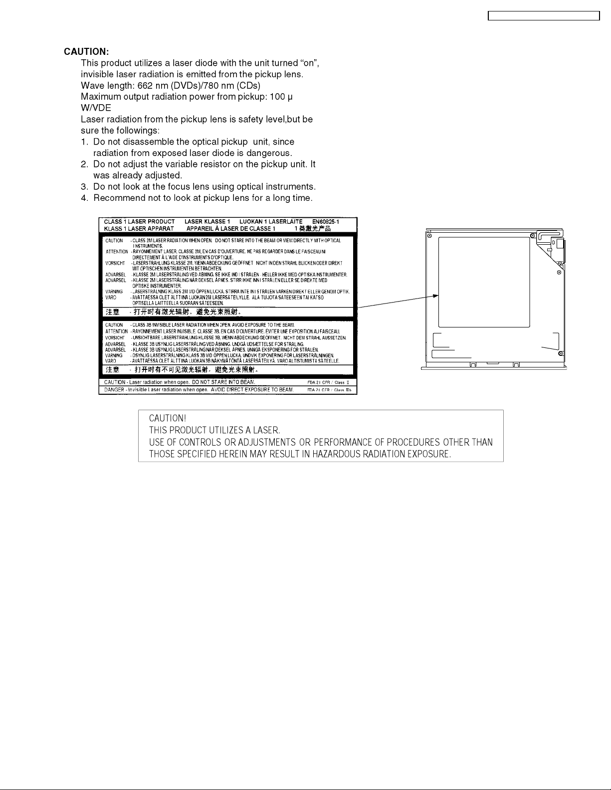
2.2. Precautiopn of Laser Diode
VW-BN1PP / VW-BN1E / VW-BN1GK /
5
VW-BN1PP / VW-BN1E / VW-BN1GK /
2.3. Service caution based on legal restrictions
2.3.1. General description about Lead Free Solder (PbF)
The lead free solder has been used in the mounting process of all electrical components on the printed circuit boards used for this
equipment in considering the globally environmental conservation.
The normal solder is the alloy of tin (Sn) and lead (Pb). On the other hand, the lead free solder is the alloy mainly consists of tin
(Sn), silver (Ag) and Copper (Cu), and the melting point of the lead free solder is higher approx.30 degrees C (86°F) more than that
of the normal solder.
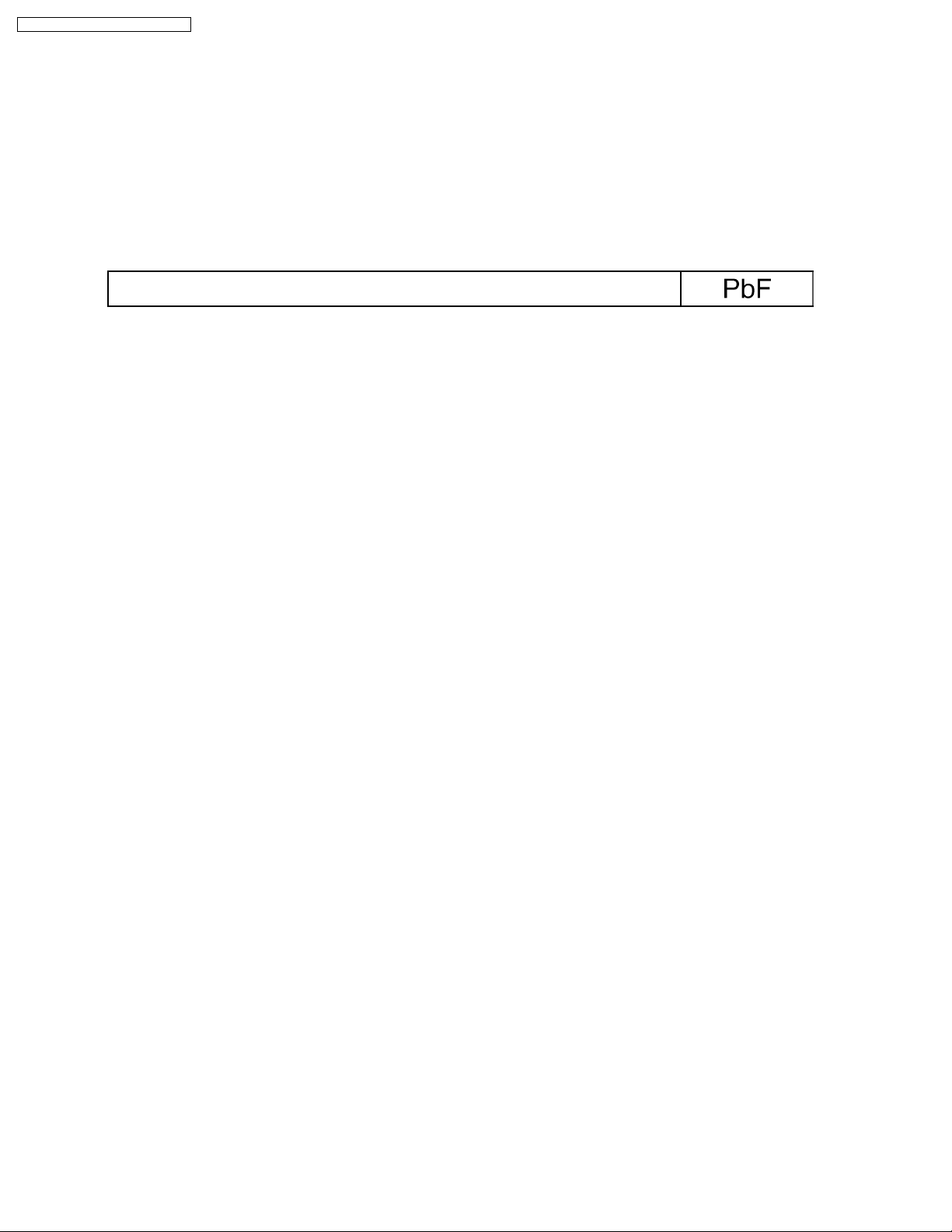
Definition of PCB Lead Free Solder being used
The letter of “PbF” is printed either foil side or components side on the PCB using the lead free solder.
(See right figure)
Service caution for repair work using Lead Free Solder (PbF)
·
The lead free solder has to be used when repairing the equipment for which the lead free solder is used.
(Definition: The letter of “PbF” is printed on the PCB using the lead free solder.)
·
To put lead free solder, it should be well molten and mixed with the original lead free solder.
·
Remove the remaining lead free solder on the PCB cleanly for soldering of the new IC.
·
Since the melting point of the lead free solder is higher than that of the normal lead solder, it takes the longer time to melt
the lead free solder.
·
Use the soldering iron (more than 70W) equipped with the temperature control after setting the temperature at 350±30
degrees C (662±86°F).
Recommended Lead Free Solder (Service Parts Route.)
·
The following 3 types of lead free solder are available through the service parts route.
RFKZ03D01K-----------(0.3mm 100g Reel)
RFKZ06D01K-----------(0.6mm 100g Reel)
RFKZ10D01K-----------(1.0mm 100g Reel)
Note
* Ingredient: tin (Sn), 96.5%, silver (Ag) 3.0%, Copper (Cu) 0.5%, Cobalt (Co) / Germanium (Ge) 0.1 to 0.3%
6

VW-BN1PP / VW-BN1E / VW-BN1GK /
3 Service Navigation
3.1. Service Information
This service manual contains technical information which will allow service personnel´s to understand and service this model.
Please place orders using the parts list and not the drawing reference numbers.
If the circuit is changed or modified, this information will be followed by supplement service manual to be filed with original service
manual.
7
VW-BN1PP / VW-BN1E / VW-BN1GK /
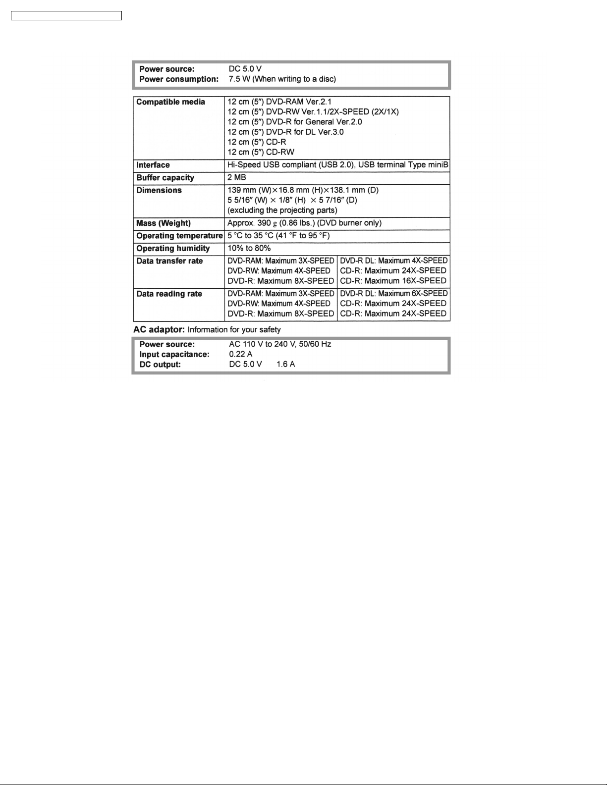
4 Specifications
8
 Loading...