Panasonic UP0KG8D User Manual

Multi Chip Discrete
Unit: mm
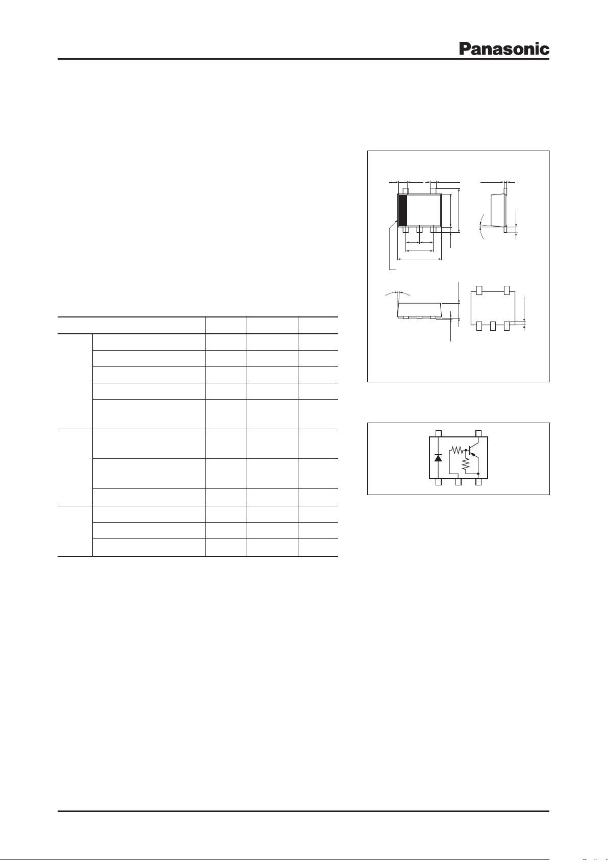
1: Anode 4: Collector
2: Base 5: Cathode
3: Emitter SSMini5-F2 Package
–0.02
+0.05
0.20(0.30)
(0.50)
1 2 3
5 4
(0.50)
1.60±0.050.55±0.05
0 to 0.02
0.10 max
1.20±0.05
1.00±0.05
1.60±0.05
0.10±0.02
(0.20)
(0.20)
5
°
5
°
Display at No.1 lead
3
4
1 2
5
Tr
SBD
UP0KG8D
Silicon epitaxial planar type (SBD)
Silicon PNP epitaxial planar type (Tr)
For digital circuits
Features
Two elements incorporated into one package (SBD + Tr)
Costs can be reduced through downsizing of the equipment and reduction of
the number of parts
Basic Part Number
MA2SD24 + UNR31A3
Absolute Maximum Ratings Ta = 25°C
Parameter Symbol Rating Unit
SBD
Tr
Overall
Reverse voltage V
Repetitive peak reverse voltage V
Forward current (Average) I
Peak forward current I
Non-repetitive peak forward
surge current
Collector-base voltage
(Emitter open)
Collector-emitter voltage
(Base open)
Collector current I
Total power dissipation P
Junction temperature T
Storage temperature T
F(AV)
I
V
V
R
RRM
FM
FSM
CBO
CEO
C
T
j
stg
Note) *: 50 Hz sine wave 1 cycle (Non-repetitive peak current)
20 V
20 V
200 mA
300 mA
1 A
-50
-50
-80
125 mW
125
–55 to +125
V
V
mA
°C
°C
Marking Symbol: 6K
Internal Connection
Publication date: November 2005 SJJ00334AED 1

UP0KG8D
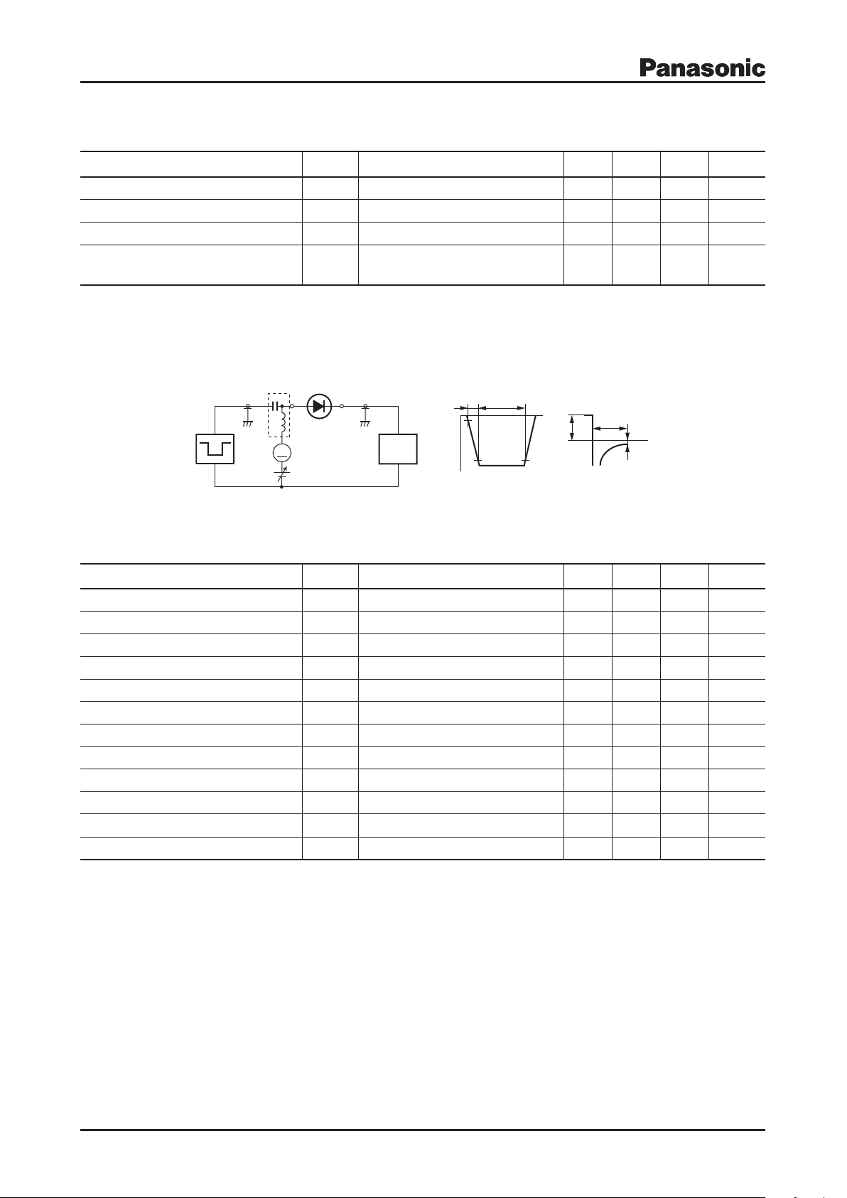
Bias Application Unit (N-50BU)
90%
Pulse Generator
(PG-10N)
Rs = 50 Ω
Wave Form Analyzer
(SAS-8130)
Ri = 50 Ω
tp = 2 µs
tr = 0.35 ns
δ = 0.05
IF = IR = 100 mA
RL = 100 Ω
10%
Input Pulse Output Pulse
I
rr
= 10 mA
t
r
t
p
t
rr
V
R
I
F
t
t
A
Electrical Characteristics Ta = 25°C±3°C
SBD
Parameter Symbol Conditions Min Typ Max Unit
Forward voltage V
Reverse current I
Terminal capacitance C
Reverse recovery time
Note) 1. Measuring methods are based on JAPANESE INDUSTRIAL STANDARD JIS C 7031 measuring methods for diodes.
2. Absolute frequency of input and output is 250 MHz
2. This product is sensitive to electric shock (static electricity, etc.). Due attention must be paid on the charge of a human body and the leakage
of current from the operating equipment.
3. *: trr measurement circuit
*
IF = 200 mA 0.50 0.58 V
F
VR = 10 V 0.1 1
R
VR = 0 V, f = 1 MHz 25 pF
t
IF = IR = 100 mA, Irr = 10 mA,
t
rr
RL = 100 W
3 ns
mA
Tr2
Parameter Symbol Conditions Min Typ Max Unit
Collector-base voltage (Emitter open) V
Collector-emitter voltage (Base open) V
Collector-base cutoff current (Emitter open) I
Collector-emitter cutoff current (Base open) I
Emitter-base cutoff current (Collector open) I
Forward current transfer ratio h
Collector-emitter saturation voltage V
Output voltage high-level V
Output voltage low-level V
CBOIC
CEOIC
CBO
CEO
EBO
FE
CE(sat)IC
OH
OL
Input resistance R
Resistance ratio R1 / R
Transition frequency f
Note) Measuring methods are based on JAPANESE INDUSTRIAL STANDARD JIS C 7030 measuring methods for transistors.
T
= -10 mA, IE = 0
= -2 mA, IB = 0
-50
-50
VCB = -50 V, IE = 0
VCE = -50 V, IB = 0
VEB = -6 V, IC = 0
VCE = -10 V, IC = -5 mA 80
= -10 mA, IB = - 0.3 mA
VCC = -5 V, VB = - 0.5 V, RL = 1 kW
-4.9
VCC = -5 V, VB = -3.5 V, RL = 1 kW
1
2
-30%
0.8 1.0 1.2
47
VCB = -10 V, IE = 2 mA, f = 200 MHz 80 MHz
- 0.1 mA
- 0.5 mA
- 0.1
mA
- 0.25
- 0.2
+30%
V
V
V
V
V
kW
2 SJJ00334AED
 Loading...