Panasonic UP05C8B User Manual

Multi Chip Discrete
3
(G)
(S)
4
1
(E)2(B)
(C)6(D)
5
Tr
FET
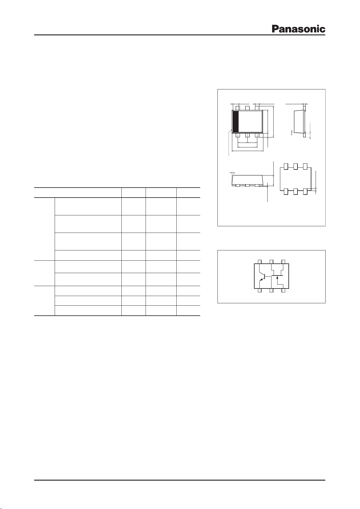
Unit: mm
1: Emitter 4: Source
2: Base 5: Drain
3: Gate 6: Collector
SSMini6-F1 Package
(0.30) 0.10±0.02
6 5 4
1 2 3
5°
5°
0.20
+0.05
–0.02
1.60±0.050.55±0.05
0.10 max.
0 to 0.02
(0.20)
1.60±0.05
1番ピン端子表示
1.20±0.05
(0.20)
1.00±0.05
(0.50)(0.50)
UP05C8B
Silicon NPN epitaxial planar type (Tr)
Silicon epitaxial planar type (CCD load device)
For CCD output circuits
Features
Two elements incorporated into one package (Tr + CCD load device)
Costs can be reduced through downsizing of the equipment and reduction of
the number of parts.
Basic Part Number
2SC3931 + CCD load device
Absolute Maximum Ratings Ta = 25°C
Parameter Symbol Rating Unit
Collector-base voltage
(Emitter open)
Collector-emitter voltage
Tr
(Base open)
Emitter-base voltage
(Collector open)
Collector current I
CCD
Limiting element voltage V
load
device
Overall
Limiting element current I
Total power dissipation
*
Junction temperature T
Storage temperature T
Note) * : Measuring on substrate at 17 mm × 10 mm × 1 mm
V
CBO
V
CEO
V
EBO
C
max
max
P
T
j
stg
30 V
20 V
3 V
15 mA
40 V
10 mA
125 mW
125
–55 to +125
°C
°C
Marking Symbol: 4F
Internal Connection
Publication date: November 2005 SJJ00333AED 1

UP05C8B
0 40 80 120
0
140
120
100
80
40
20
60
Total power dissipation P
T
(
mW
)
Ambient temperature Ta (°C
)
UN05C8B_PT-T
a
Electrical Characteristics Ta = 25°C±3°C
Tr
Parameter Symbol Conditions Min Typ Max Unit
Collector-base voltage (Emitter open) V
Emitter-base voltage (Collector open) V
Base-emitter voltage V
Forward current transfer ratio h
Reverse transfer capacitance
(Common emitter)
Transition frequency f
CBOIC
EBOIE
BE
FE
C
T
Noise figure NF VCB = 6 V, IE = -1 mA, f = 100 MHz 3.3 dB
Power gain G
Note) Measuring methods are based on JAPANESE INDUSTRIAL STANDARD JIS C 7030 measuring methods for transistors.
CCD Load Device
Parameter Symbol Conditions Min Typ Max Unit
= 10 mA, IE = 0 30 V
= 10 mA, IC = 0 3 V
VCE = 6 V, IC = 1 mA 720 mV
VCE = 6 V, IC = 1 mA 65 160
VCB = 6 V, IE = -1 mA, f = 10.7 MHz 0.8 pF
re
VCB = 6 V, IE = -1 mA, f = 200 MHz 640 MHz
VCB = 6 V, IE = -1 mA, f = 100 MHz 24 dB
P
Pinchi off current I
Output impedance Z
Note) Measuring methods are based on JAPANESE INDUSTRIAL STANDARD JIS C 7030 measuring methods for transistors.
VDS = 10 V, VG = 0 3.5 5.5 mA
P
VDS = 10 V, VG = 0 0.05 MW
O
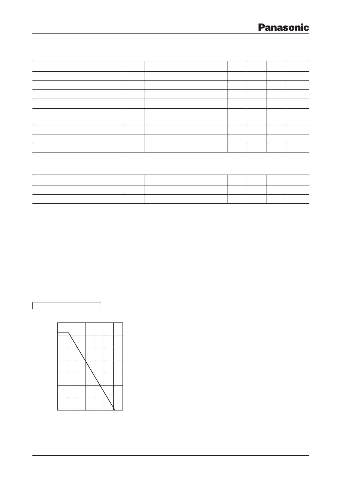
Common characteristics chart
PT T
a
2 SJJ00333AED
 Loading...