

Panasonic TX-P42V10B, TX-P42V10E Service manual
ORDER NO. PCZ0905073CE
Plasma Television
Model No. TX-P42V10B
TX-P42V10E
GPF12DE Chassis
© Panasonic Corporation 2009.
Unauthorized copying and distribution is a violation
of law.

TABLE OF CONTENTS
1 Safety Precautions ---------------------------------------------------3
1.1. General Guidelines--------------------------------------------3
1.2. Touch-Current Check -----------------------------------------3
2 Warning-------------------------------------------------------------------4
2.1. Prevention of Electrostatic Discharge (ESD) to
Electrostatically Sensitive (ES) Devices -----------------
2.2. About lead free solder (PbF) ----- ------ ----- ------ ------ ---- 5
3 Service Navigation----------------------------------------------------6
3.1. Service Hint ------------------------------------------- ------ ---- 6
3.2. Applicable signals ---------------------------------------------7
4 Specifications----------------------------------------------------------8
5 Service Mode --------------------------------------------------------- 10
5.1. How to enter into Service Mode-------------------------- 10
5.2. Service tool mode ------------ ------ ------------------------- 12
5.3. Hotel mode---------------------------------------------------- 13
6 Troubleshooting Guide-------------------------------------------- 14
6.1. Check of the IIC bus lines --------------------------------- 14
6.2. Power LED Blinking timing chart------------------------- 15
6.3. No Power ------------------------------------------------------ 16
6.4. No Picture ----------------------------------------------------- 17
6.5. Local screen failure ----------------------------------------- 18
7 Disassembly and Assembly Instructions------------------- 19
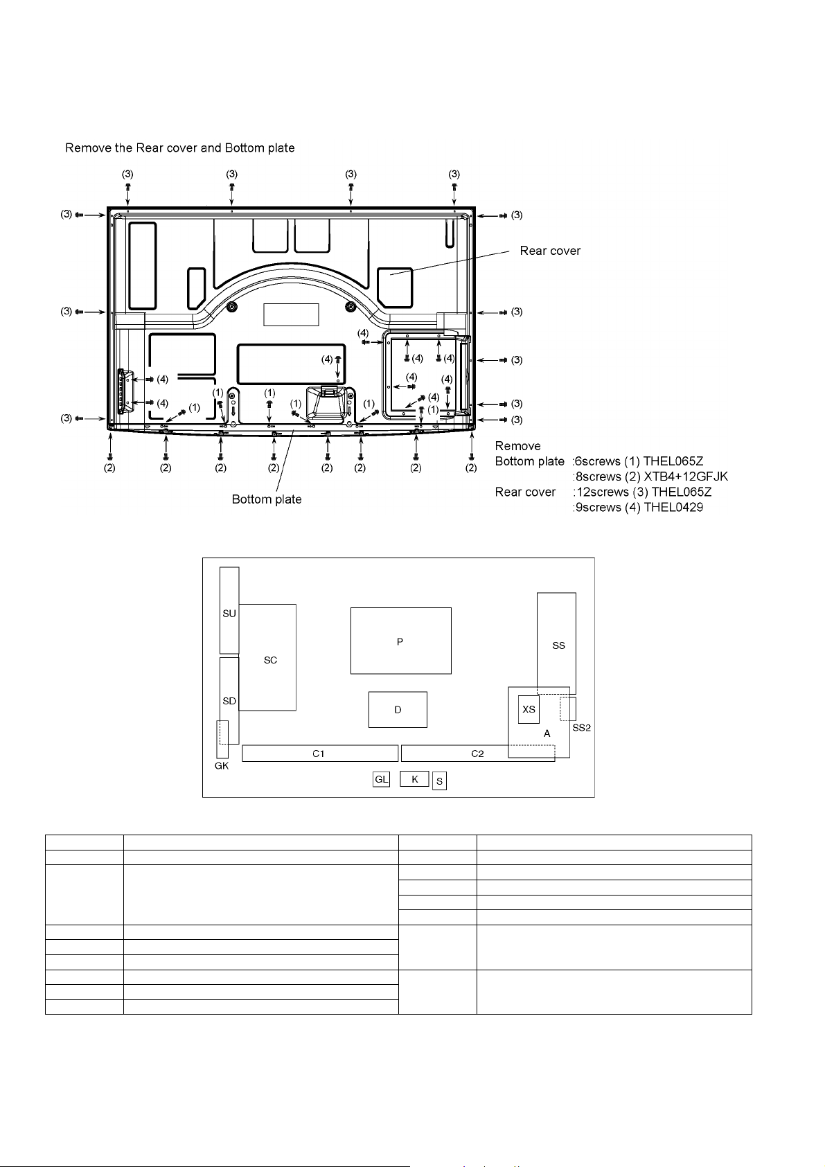
7.1. Remove the Rear cover------------------------------------ 19
7.2. Remove the Fan --------------------------------------------- 19
7.3. Remove the P-Board --------------------------------------- 19
7.4. Remove the Side terminal cover and Rear
terminal cover-------------------------------------------------
7.5. Remove the Tuner unit------------------------------------- 20
7.6. Remove the XS-Board ------------------------------------- 20
7.7. Remove the A-Board --------------------------------------- 21
7.8. Remove the D-Board --------------------------------------- 21
7.9. Remove the Speakers-------------------------------------- 21
7.10. Remove the Control button unit--------------------------22
7.11. Remove the GK-Board ------------------------------------- 22
7.12. Remove the SU-Board ------------------------------------- 22
7.13. Remove the SD-Board ------------------------------------- 23
7.14. Remove the SC-Board ------------------------------------- 23
7.15. Remove the SS2-Board------------------------------------ 23
7.16. Remove the SS-Board ------------------------------------- 24
7.17. Remove the Hanger metals and the Stand
brackets--------------------------------------------------------
7.18. Remove the C1-Board-------------------------------------- 24
7.19. Remove the C2-Board-------------------------------------- 24
7.20. Remove the Plasma panel section from the
Cabinet assy (glass) ----------------------------------------
7.21. Remove the S-Board --------------------------------------- 25
7.22. Remove the K-Board --------------------------------------- 26
7.23. Remove the GL-Board ------------------------------------- 26
7.24. Replace the plasma panel--------------------------------- 26
8 Measurements and Adjustments ------------------------------ 27
8.1. Adjustment Procedure-------------------------------------- 27
8.2. Adjustment ---------------------------------------------------- 30
9 Block Diagram ------------------------------------------------------- 35
9.1. Main Block Diagram----------------------------------------- 35
9.2. Block (1/5) Diagram -------------------------------- ------ -- 36
9.3. Block (2/5) Diagram----------------------------------------- 37
9.4. Block (3/5) Diagram----------------------------------------- 38
9.5. Block (4/5) Diagram----------------------------------------- 39
9.6. Block (5/5) Diagram----------------------------------------- 40
10 Wiring Co nnecti on Diagram ------------------------------------- 41
10.1. Caution statement. ------------------------------------------ 41
10.2. Wiring (1) ------ ------------------------------------------------ 41
10.3. Wiring (2) ------ ------------------------------------------------ 42
10.4. Wiring (3) ------ ------------------------------------------------ 43
10.5. Wiring (4) ------ ------------------------------------------------ 44
10.6. Wiring (5) ------ ------------------------------------------------ 45
PAGE PAGE
10.7. Wiring (6)--------------------------------------- ------ ------ ----46
10.8. Wiring (7)--------------------------------------- ------ ------ ----47
10.9. Wiring (8)--------------------------------------- ------ ------ ----48
10.10. Wiring (9)--------------------------------- ------ ------ ------ ----49
11 Schematic Diagram-------------------------------------------------51
4
19
24
25
11.1. Schematic Diagram Note ------- ----- ------ ----------------51
11.2. P-Board (1/2) Schematic Diagram-----------------------52
11.3. P-Board (2/2) Schematic Diagram-----------------------53
11.4. GK, GL, K, S and XS-Board Schematic Diagram----54
11.5. A-Board (1/22) Schematic Diagram ---------------------55
11.6. A-Board (2/22) Schematic Diagram ---------------------56
11.7. A-Board (3/22) Schematic Diagram ---------------------57
11.8. A-Board (4/22) Schematic Diagram ---------------------58
11.9. A-Board (5/22) Schematic Diagram ---------------------59
11.10. A-Board (6/22) Schematic Diagram ---------------------60
11.11. A-Board (7/22) Schematic Diagram ---------------------61
11.12. A-Board (8/22) Schematic Diagram ---------------------62
11.13. A-Board (9/22) Schematic Diagram ---------------------63
11.14. A-Board (10/22) Schematic Diagram --- ------ ------ ----64
11.15. A-Board (11/22) Schematic Diagram--------------------65
11.16. A-Board (12/22) Schematic Diagram --- ------ ------ ----66
11.17. A-Board (13/22) Schematic Diagram --- ------ ------ ----67
11.18. A-Board (14/22) Schematic Diagram --- ------ ------ ----68
11.19. A-Board (15/22) Schematic Diagram --- ------ ------ ----69
11.20. A-Board (16/22) Schematic Diagram --- ------ ------ ----70
11.21. A-Board (17/22) Schematic Diagram --- ------ ------ ----71
11.22. A-Board (18/22) Schematic Diagram --- ------ ------ ----72
11.23. A-Board (19/22) Schematic Diagram --- ------ ------ ----73
11.24. A-Board (20/22) Schematic Diagram --- ------ ------ ----74
11.25. A-Board (21/22) Schematic Diagram --- ------ ------ ----75
11.26. A-Board (22/22) Schematic Diagram --- ------ ------ ----76
11.27. D-Board (1/4) Schematic Diagram-----------------------77
11.28. D-Board (2/4) Schematic Diagram-----------------------78
11.29. D-Board (3/4) Schematic Diagram-----------------------79
11.30. D-Board (4/4) Schematic Diagram-----------------------80
11.31. C1-Board (1/2) Schematic Diagram---------------------81
11.32. C1-Board (2/2) Schematic Diagram---------------------82
11.33. C2-Board (1/2) Schematic Diagram---------------------83
11.34. C2-Board (2/2) Schematic Diagram---------------------84
11.35. SC-Board (1/4) Schematic Diagram---------------------85
11.36. SC-Board (2/4) Schematic Diagram---------------------86
11.37. SC-Board (3/4) Schematic Diagram---------------------87
11.38. SC-Board (4/4) Schematic Diagram---------------------88
11.39. SS-Board (1/2) Schematic Diagram---------------------89
11.40. SS-Board (2/2) and SS2-Board Schematic
Diagram --------------------------------------------------------
12 Printed Circuit Board-----------------------------------------------91
12.1. P-Board---------------------------------------------------------91
12.2. GK, K, S and SS2-Board-----------------------------------94
12.3. GL, and XS-Board -------------------------------------------95
12.4. A-Board---------------------------------------------------------96
12.5. D-Board---------------------------------------------------------98
12.6. C1-Board----------------------------------------------------- 100
12.7. C2-Board----------------------------------------------------- 101
12.8. SC-Board----------------------------------------------------- 102
12.9. SS-Board-----------------------------------------------------105
13 Exploded View and Replacement Parts List--------------107
13.1. Exploded View and Mechanical Replacement
Parts List -----------------------------------------------------
13.2. Electrical Replacement Parts List---------------------- 115
90
107
2
1 Safety Precautions
1.1. General Guidelines
1. When servicing, observe the original lead dress. If a short circuit is found, replace all parts which have been overheated or
damaged by the short circuit.
2. After servicing, see to it that all the protective devices such as insulation barriers, insulation papers shields are properly
installed.
3. After servicing, make the following leakage current checks to prevent the customer from being exposed to shock hazards.
4. When servicing, observe the original lead dress. If a short circuit is found, replace all parts which have been overheated or
damaged by the short circuit.
5. After servicing, see to it that all the protective devices such as insulation barriers, insulation papers shields are properly
installed.
6. After servicing, make the following leakage current checks to prevent the customer from being exposed to shock hazards.
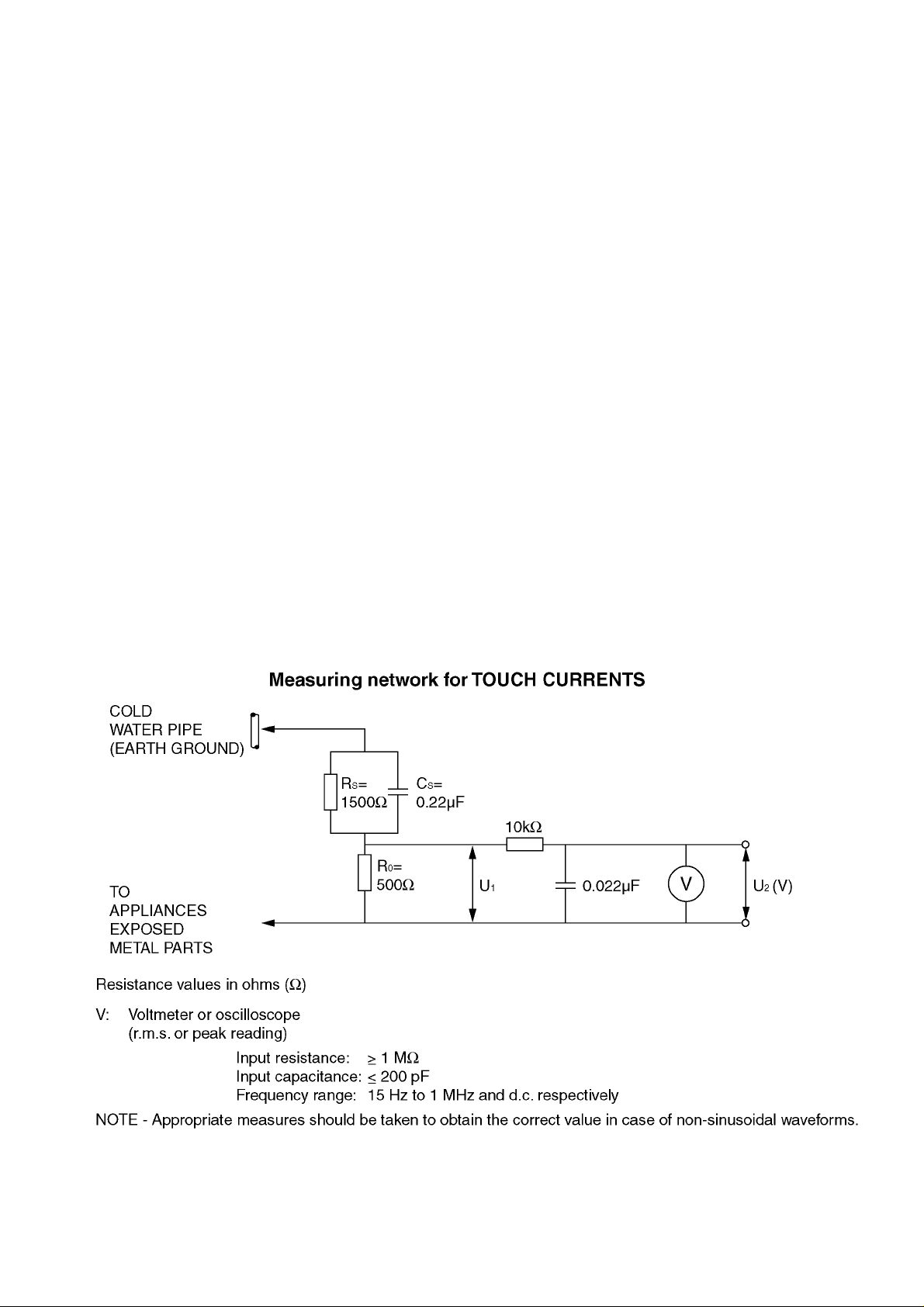
1.2. Touch-Current Check
1. Plug the AC cord directly into the AC outlet. Do not use an isolation transformer for this check.
2. Connect a measuring network for touch currents between each exposed metallic part on the set and a good earth ground
such as a water pipe, as shown in Figure 1.
3. Use Leakage Current Tester (Simpson 228 or equivalent) to measure the potential across the measuring network.
4. Check each exposed metallic part, and measure the voltage at each point.
5. Reserve the AC plug in the AC outlet and repeat each of the above measure.
6. The potential at any point (TOUGH CURRENT) expressed as voltage U
For a. c.: U1 = 35 V (peak) and U2 = 0.35 V (peak);
For d. c.: U
Note:
The limit value of U
mA d. c.
The limit value U
7. In case a measurement is out of the limits specified, there is a possibility of a shock hazard, and the equipment should be
repaired and rechecked before it is returned to the customer.
= 1.0 V,
1
= 0.35 V (peak) for a. c. and U1 = 1.0 V for d. c. correspond to the values 0.7 mA (peak) a. c. and 2.0
2
= 35 V (peak) for a. c. correspond to the value 70 mA (peak) a. c. for frequencies greater than 100 kHz.
1
and U2, does not exceed the following values:
1
Figure 1
3

2Warning
2.1. Prevention of Electrostatic Discharge (ESD) to Electrostatically Sensitive (ES) Devices
Some semiconductor (solid state) devices can be damaged easily by static electricity. Such components commonly are called Electrostatically Sensitive (ES) Devices. Examples of typical ES devices are integrated circuits and some field-effect transistors and
semiconductor [chip] components. The following techniques should be used to help reduce the incid ence of component damage
caused by electrostatic discharge (ESD).
1. Immediately before handling any semiconductor component or semiconductor-equipped assembly, drain off any ESD on your
body by touching a known earth ground. Alternatively, obtain and wear a commercially available discharging ESD wrist strap,
which should be removed for potential shock reasons prior to applying power to the unit under test.
2. After removing an electrical assembly equipped with ES devices, place the assembly on a conductive surface such as a luminum foil, to prevent electrostatic charge buildup or exposure of the assembly.
3. Use only a grounded-tip soldering iron to solder or unsolder ES devices.
4. Use only an anti-static solder removal device. Som e solder removal devices not classified as [anti-static (ESD protected)] can
generate electrical charge sufficient to damage ES devices.
5. Do not use freon-propelled chemicals. These can generate electrical charges sufficient to damage ES devices.
6. Do not remove a replacement ES device from its protective package until immediately before you are ready to install it. (Most
replacement ES devices are packaged with leads electrically shorted together by conductive foam, aluminum foil or comparable conductive material).
7. Immediately before removing the protective material from the leads of a replacement ES device, touch the protective material
to the chassis or circuit assembly into which the device will be installed.
Caution
Be sure no power is applied to the chassis or circuit, and observe all other safety precautions.
8. Minimize bodily motions when handling unpackaged replacement ES devices. (Otherwise ham less motion such as the brushing together of your clothes fabric or the lifting of your foot from a carpeted floor can generate static electricity (ESD) sufficient
to damage an ES device).
4
2.2. About lead free solder (PbF)
Note: Lead is listed as (Pb) in the periodic table of elements.
In the information below, Pb will refer to Lead solder, and PbF will refer to Lead Free Solder.
The Lead Free Solder used in our manufacturing proc ess and discussed below is (Sn+Ag+Cu).
That is Tin (Sn), Silver (Ag) and Copper (Cu) although other types are available.
This model uses Pb Free solder in it’s manufacture due to environmental conservation issues. For service and repair work, we’d
suggest the use of Pb free solder as well, although Pb solder may be used.
PCBs manufactured using lead free solder will have the PbF within a leaf Symbol PbF stamped on the back of PCB.
Caution
• Pb free solder has a higher melting point than standard solder. Typically the melting point is 50 ~ 70 °F (30~40 °C) higher. Please
use a high temperature soldering iron and set it to 700 ± 20 °F (370 ± 10 °C).
• P b free solder will tend to splash when heated too high (about 1100 °F or 600 °C).
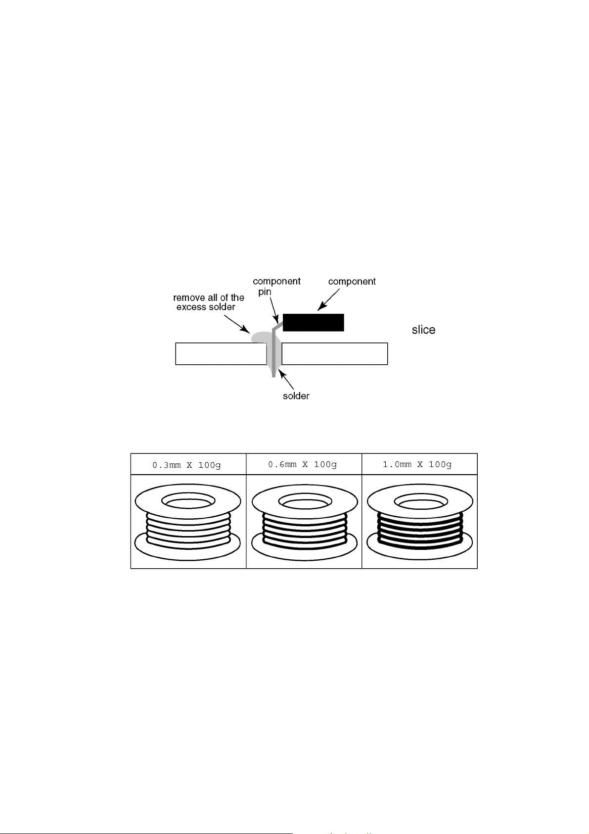
If you must use Pb solder, please completely remove all of the Pb free solder on the pins or solder area before applying Pb sol der. If this is not practical, be sure to heat the Pb free solder until it melts, before applying Pb solder.
• After applying PbF solder to double layered boards, please check the component side for excess solder which may flow onto the
opposite side. (see figure below)
Suggested Pb free solder
There are several kinds of Pb free solder available for purchase. This product uses Sn+Ag+Cu (tin, silver, copper) solder. However, Sn+Cu (tin, copper), Sn+Zn+Bi (tin, zinc, bismuth) solder can also be used.
5
3 Service Navigation
3.1. Service Hint
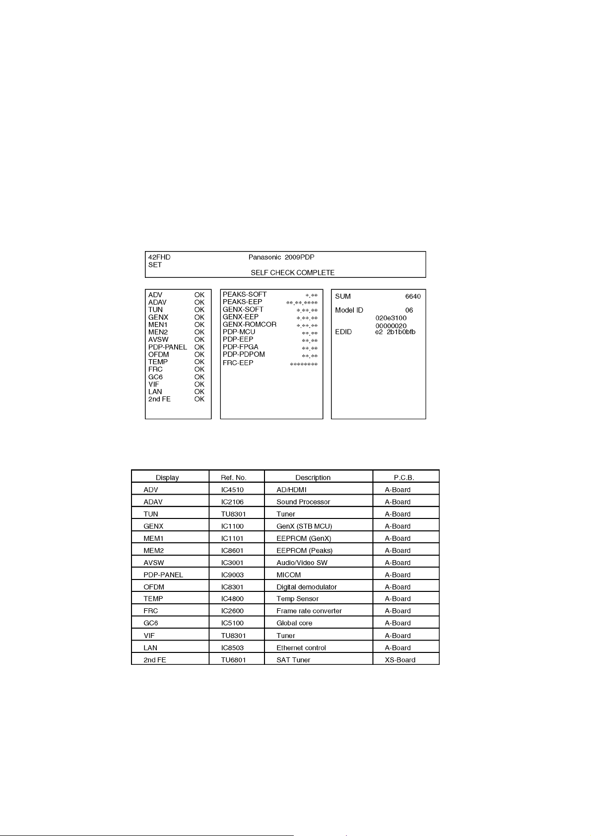
Board Name Function Board Name Function
P Power Supply C1 Data Driver (Lower Right)
A DC-DC Converter, Tuner
Speaker out, AV Terminal, AV Switch, PC
Digital Signal Processor, SYSTEM MPU, HDMI Switch
Peaks-AVC, Ethernet
D Format Converter, Plasma AI, Sub-Field Processor SU Scan out (Upper)
XS Sat Tuner
GL SD LED
K Remote receiver, Power LED, C.A.T.S. sensor SD Scan out (Lower)
S Power Switch
GK Key Switch
C2 Data Driver (Lower Left)
SC Scan Drive
SS Sustain Drive
SS2 Sustain out (Lower)
Non-serviceable.
SU-Board should be exchanged for service.
Non-serviceable.
SD-Board should be exchanged for service.
6
3.2. Applicable signals
COMPONENT (Y, PB, PR), HDMI
* Mark: Applicable input signal for Component (Y, PB, PR) and HDMI
Signal name COMPONENT HDMI
525 (480) / 60i * *
525 (480) / 60p * *
625 (576) / 50i * *
625 (576) / 50p * *
750 (720) / 60p * *
750 (720) / 50p * *
1,125 (1,080) / 60i * *
1,125 (1,080) / 50i * *
1,125 (1,080) / 60p *
1,125 (1,080) / 50p *
1,125 (1,080) / 24p *
PC (from D-sub 15P)
Applicable input signal for PC is basically compatible to VESA standard timing.
Signal name Horizontal frequency (kHz) Vertical frequency (Hz)
640 × 400 @70 Hz 31.47 70.07
640 × 480 @60 Hz 31.47 59.94
640 × 480 @75 Hz 37.50 75.00
800 × 600 @60 Hz 37.88 60.32
800 × 600 @75 Hz 46.88 75.00
800 × 600 @85 Hz 53.67 85.06
852 × 480 @60 Hz 31.44 59.89
1,024 × 768 @60 Hz 48.36 60.00
1,024 × 768 @70 Hz 56.48 70.07
1,024 × 768 @75 Hz 60.02 75.03
1,024 × 768 @85 Hz 68.68 85.00
1,280 × 768 @60 Hz 47.70 60.00
1,280 × 1,024 @60 Hz 63.98 60.02
1,366 × 768 @60 Hz 48.39 60.04
Macintosh13 inch (640 × 480) 35.00 66.67
Macintosh16 inch (832 × 624) 49.73 74.55
Macintosh21 inch (1,152 × 870) 68.68 75.06
PC (from HDMI terminal)
Applicable input signal for PC is basically compatible to HDMI standard timing.
Signal name Horizontal frequency (kHz) Vertical frequency (Hz)
640 × 480 @60 Hz 31.47 60.00
750 (720) / 60p 45.00 60.00
1,125 (1,080) / 60p 67.50 60.00
Note
• S ignals other than above may not be displayed properly.
• The above signals are reformatted for optimal viewing on your display.
• P C signal is magnified or compressed for display, so that it may not be possible to show fine detail with sufficient clarity.
7

4 Specifications
Power Source AC 220-240 V, 50 / 60 Hz
Power Consumption 350 W
Power Consumption in Standby condition 0.4 W (Without monitor out recording)
32 W (With monitor out recording)
Display panel
Aspect Ratio 16:9
Visible screen size 106 cm (diagonal) 921 mm (W) × 518 mm (H)
Number of pixels 2,073,600 (1,920 (W) × 1,080 (H)) [5,760 × 1,080 dots]
Sound
Speaker 140 mm × 35 mm × 2 pcs, 6 Ω
Audio Output 20 W ( 10 W + 10 W ), 10 % THD
Headphones M3 (3.5 mm) stereo mini Jack × 1
PC signals VGA, SVGA, WVGA, XGA
SXGA, WXGA ...... (compressed)
Horizontal scanning frequency 31 - 69 kHz
Vertical scanning frequency 59 - 86 Hz
Receiving Systems / Band name (B only)
DVB-S / S2
(freesat Other Sat.) :
DVB-T : Digital terrestrial services via UHF aerial input.
PAL I : UHF E21-68
PAL 525/60 : Playback of NTSC tape from some PAL Video recorders (VCR)
M.NTSC : Playback from M.NTSC Video recorders (VCR).
NTSC (AV input only) : Playback from NTSC Video recorders (VCR).
Receiving Systems / Band name (E only)
PAL B, G, H, I,
SECAM B, G, SECAM L, L’ :
PAL D, K, SECAM D, K : VHF R1 - R2
PAL 525/60 : Playback of NTSC tape from some PAL Video recorders (VCR)
DVB-T : Digital terrestrial services
DVB-C : Digital cable services
DVB-S / S2 : Digital satellite services
M.NTSC : Playback from M.NTSC Video recorders (VCR).
NTSC (AV input only) : Playback from NTSC Video recorders (VCR).
O TV signals may not be received in some areas.
Satellite dish input Female F-type 75 Ω
freesat services via Satellite dish input.
Receiver frequency range - 950 MHz to 2,150 MHz
LNB Power and Polarisation - Vertical: +13 V
Horizontal: +18 V
Current: Max. 500 mA
(overload protection)
22 kHz Tone - Frequency: 22 kHz ± 2 kHz
Amplitude: 0.6 V ± 0.2 V
Symbol Rate - Max. 30 MS/s
FEC Mode - 1/2, 3/5, 2/3, 3/4, 4/5, 5/6, 8/9, 9/10
Demodulation - QPSK, 8PSK
Not available for DiSEqC control.
or NTSC disc playback from DVD player and recorder.
VHF E2 - E12
VHF H1 - H2 (ITALY)
VHF A - H (ITALY)
UHF E21 - E69
CATV (S01 - S05)
CATV S1 - S10 (M1 - M10)
CATV S11 - S20 (U1 - U10)
CATV S21 - S41 (Hyperband)
VHF R3 - R5
VHF R6 - R12
UHF E21 - E69
Receiver frequency range - 950 MHz to 2,150 MHz
LNB Power and Polarisation - Vertical: +13 V
Horizontal: +18 V
Current: Max. 500 mA
(overload protection)
22 kHz Tone - Frequency: 22 kHz ± 2 kHz
Amplitude: 0.6 V ± 0.2 V
Symbol Rate - Max. 30 MS/s
FEC Mode - 1/2, 3/5, 2/3, 3/4, 4/5, 5/6, 8/9, 9/10
Demodulation - QPSK, 8PSK
DisEqC - Version 1.0
8

Aerial input UHF (B only), VHF/UHF (E only)
Operating Conditions
Temperature: 0 °C - 35 °C
Humidity: 20 % - 80 % RH (non-condensing)
Connection Terminals
AV1 (Scart terminal) 21 Pin terminal (Audio/Video in, Audio/Video out, RGB in, Q-Link)
AV2 (Scart terminal) 21 Pin terminal (Audio/Video in, Audio/Video out, RGB in, S-Video in, Q-Link)
AV3
VIDEO RCA PIN Type × 1 1.0 V [p-p] (75 Ω)
S-VIDEO Mini DIN 4-pin Y:1.0 V [p-p] (75 Ω) C:0.286 V [p-p] (75 Ω)
AUDIO L - R RCA PIN Type × 2 0.5 V [rms]
COMPONENT
VIDEO Y 1.0 V [p-p] (including synchronization)
P
, P
B
R
± 0.35 V [p-p]
AUDIO L - R RCA PIN Type × 2 0.5 V [rms]
Others
HDMI1 / 2 / 3 / 4 TYPE A Connectors HDMI™ (Version 1.3a with Deep Colour x.v.Colour™)
O This TV supports [HDAVI Control 4] function.
PC HIGH-DENSITY D-SUB 15PIN R, G, B/ 0.7 V [p-p] (75 Ω)
HD, VD/TTL Level 2.0 - 5.0 V [p-p] (high impedance)
Card slot SD Card slot × 1
ETHERNET RJ45, IEEE802.3 10BASE-T / 100BASE-TX
Output
AUDIO L - R RCA PIN Type × 2 0.5 V [rms] (high impedance)
DIGITAL AUDIO OUT PCM / Dolby Digital, Fiber optic
Dimensions (W × H × D) 1,052 mm × 709 mm × 332 mm (With Pedestal)
1,052 mm × 668 mm × 84 mm (TV only)
Mass 29.0 kg Net (With Pedestal)
27.0 kg Net (TV only)
Note
• Design and Specifications are subject to change without notice. Mass and Dimensions shown are approximate.
• This equipment complies with the EMC standards listed below.
EN55013, EN61000-3-2, EN61000-3-3, EN55020, EN55022, EN55024.
• Pedestal: ST-42CS3WG / ST-50CS3WG (For safety approval)
9
5 Service Mode
5.1. How to enter into Service Mode
While pressing [VOLUME ( - )] button of the main unit, press [0] button of the remote control three times within 2 seconds.
5.1.1. Key command
[1] button...Main items Selection in forward direction
[2] button...Main items Selection in reverse direction
[3] button...Sub items Selection in forward direction
[4] button...Sub items Selection in reverse direction
[RED] button...All Sub items Selection in forward direction
[GREEN] button...All Sub items Selection in reverse direction
[VOL] button...Value of sub items change in forward direction ( + ), in reverse direction ( - )
10
5.1.2. Contents of adjustment mode
• Value is shown as a hexadecimal number.
• Preset value differs depending on models.
• A fter entering the adjustment mode, take note of the value in each item before starting adjustment.
5.1.3. How to exit
Switch off the power with the [POWER] button on the main unit or the [POWER] button on the remote control.
11
5.2. Service tool mode
5.2.1. How to access
1. Select [SRV-TOOL] in Service Mode.
2. Press [OK] button on the remote control.
5.2.2. Display of SOS History
SOS History (Number of LED blinking) indication.
From left side; Last SOS, before Last, three occurrence before, 2nd occurrence after shipment, 1st occurrence after shipment.
This indication will be cleared by [Self-check indication and forced to factory shipment setting].
5.2.3. POWER ON Time, On/Off
Note : To display Time, On/Off menu, highlight position, then press MUTE for 3sec.
Time : Cumulative power on time, indicated hour : minute by decimal
On/Off : Number of On/Off switching by decimal
Note : This indication will not be cleared by either of the self-checks or any other command.
5.2.4. Exit
1. Disconnect the AC cord from wall outlet or switch off the power with [ Power ] button on the main unit.
12
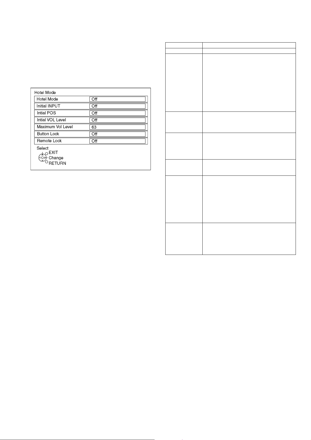
5.3. Hotel mode
1. Purpose
Restrict a function for hotels.
2. Access command to the Hotel mode setup menu
In order to display the Hotel mode setup menu, please
enter the following command (within 2 second).
[TV] : Vol. [Down] + [REMOTE] : AV (3 times)
Then, the Hotel mode setup menu is displayed.
3. To exit the Hotel mode setup menu
Disconnect AC power cord from wall outlet.
4. Explain the Hotel mode setup menu
item Function
Hotel Mode Select hotel mode ON/OFF
Initial INPUT Select input signal modes.
Set the input, when each time power is switched
on.
Selection :
Off/Analogue/DVB-S/DVB-T/AV1/AV2/AV2S/AV3/
AV3S/COMPONENT/PC/HDMI1/HDMI2/HDMI3/
HDMI4
• Off: give priority to a last memory. However,
Euro model is compulsorily set to TV.
• AVnS/AVnC: only Euro model selectable
• PC: selectable with VGA option
Initial POS Select programme number.
Initial VOL level Adjust the volume when each time power is
Maximum VOL
level
Button lock Select local key conditions.
Remote lock Select remote control key conditions.
Selection :
Off/0 to 99
• Off: give priority to a last memory
switched on.
Selection/Range :
Off/0 to 63
• Off: give priority to a last memory
Adjust maximum volume.
Range :
0 to 63
Selection :
Off/SETUP/MENU/ALL
• Off: altogether valid
• SETUP: only F-key is invalid
(Tuning guide(menu) can not be selected.)
• MENU: only F-key is invalid
(only Volume/Mute can be selected.)
• ALL: altogether invalid.
Selection :
Off/SETUP/MENU
• Off: altogether valid
• SETUP: only Setup menu is invalid
• MENU: Picture/Sound/Setup menu are invalid
13
6 Troubleshooting Guide
Use the self-check function to test the unit.
1. Checking the IIC bus lines
2. Power LED Blinking timing
6.1. Check of the IIC bus lines
6.1.1. How to access
Self-check indication only:
Produce TV reception screen, and while pressing [VOLUME ( - )] button on the main unit, press [OK] b utton on the remote control
for more than 3 seconds.
Self-check indication and forced to factory shipment setting:
Produce TV reception screen, and while pressing [VOLUME ( - )] button on the ma in unit, press [MENU] button on the remote con-
trol for more than 3 seconds.
6.1.2. Screen display
6.1.3. Check Point
Confirm the following parts if NG was displayed.
6.1.4. Exit
Disconnect the AC cord from wall outlet or switch off the power with [ Power ] button on the main unit.
14
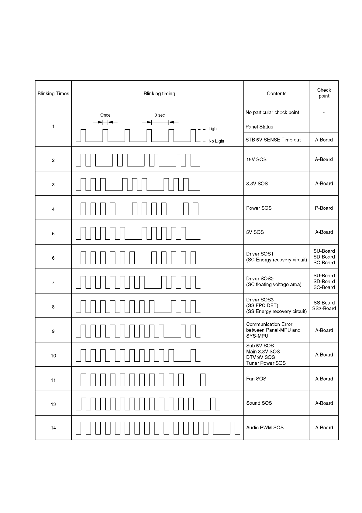
6.2. Power LED Blinking timing chart
1. Subject
Information of LED Flashing timing chart.
2. Contents
When an abnormality has occurred the unit, the protection circuit operates and reset to the stand by mode. At this time, the
defective block can be identified by the number of blinks of the Power LED on the front panel of the unit.
15
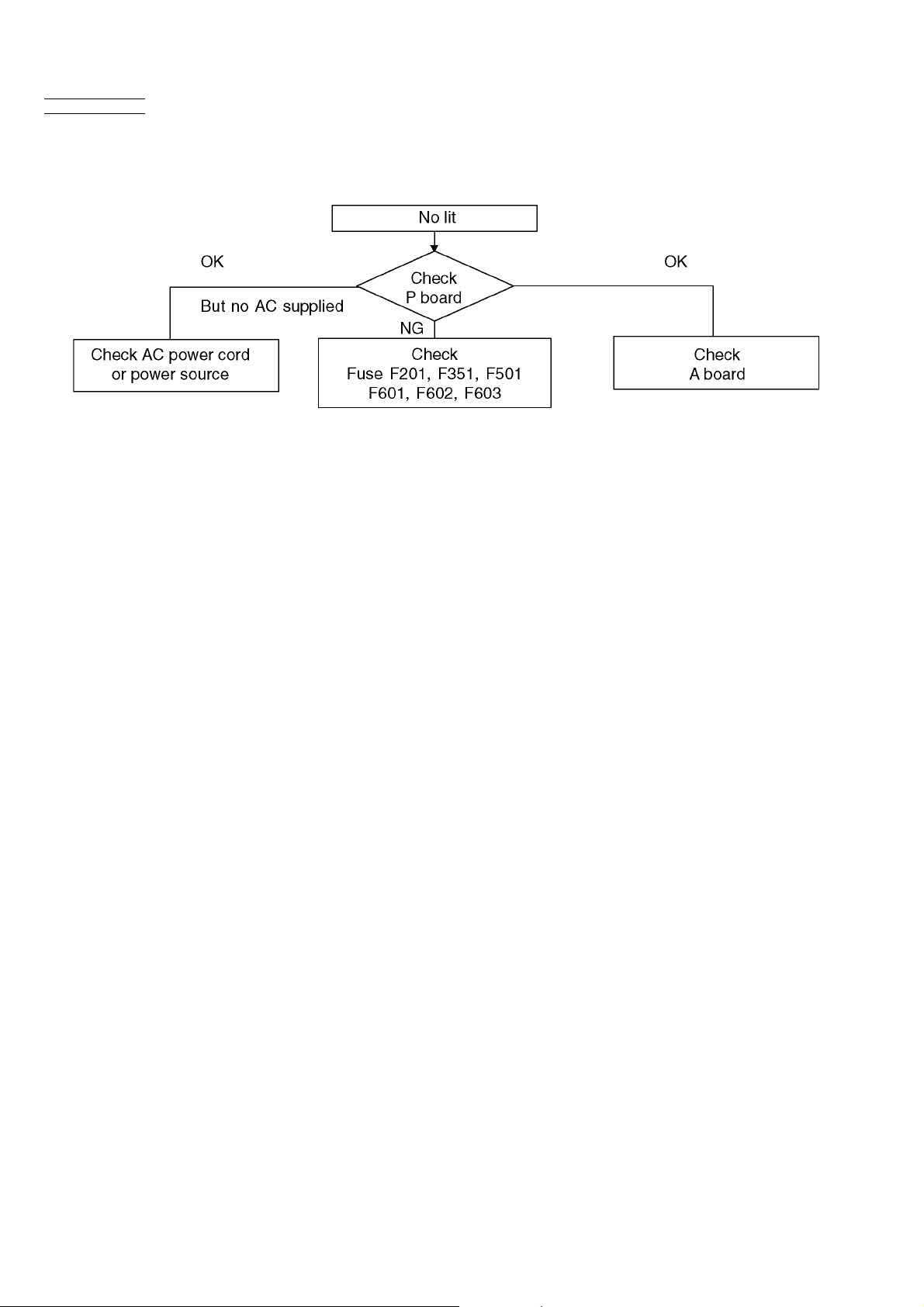
6.3. No Power
First check point
There are following 2 states of No Power indication by power LED.
1. No lit
2. Red is lit then turns red blinking a few seconds later. (See 6.2.)
16
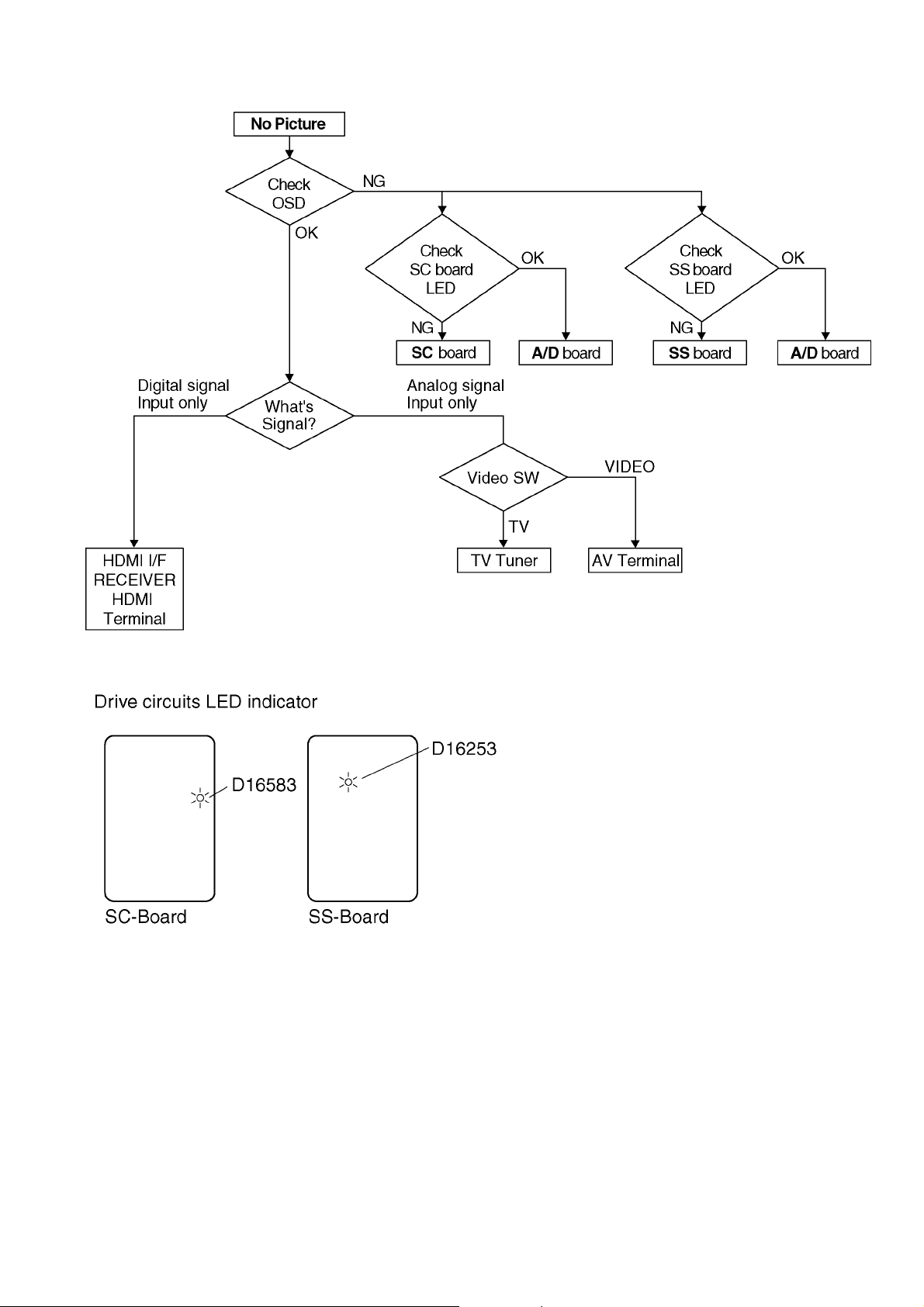
6.4. No Picture
17
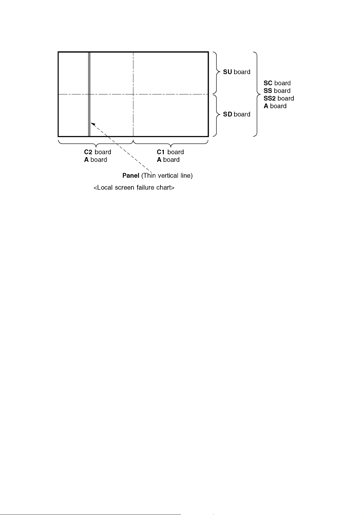
6.5. Local screen failure
Plasma display may have local area failure on the screen. Fig-1 is the possible defect P.C.B. for each local area.
Fig-1
18
7 Disassembly and Assembly Instructions
7.1. Remove the Rear cover
1. See Service Hint (Section 3)
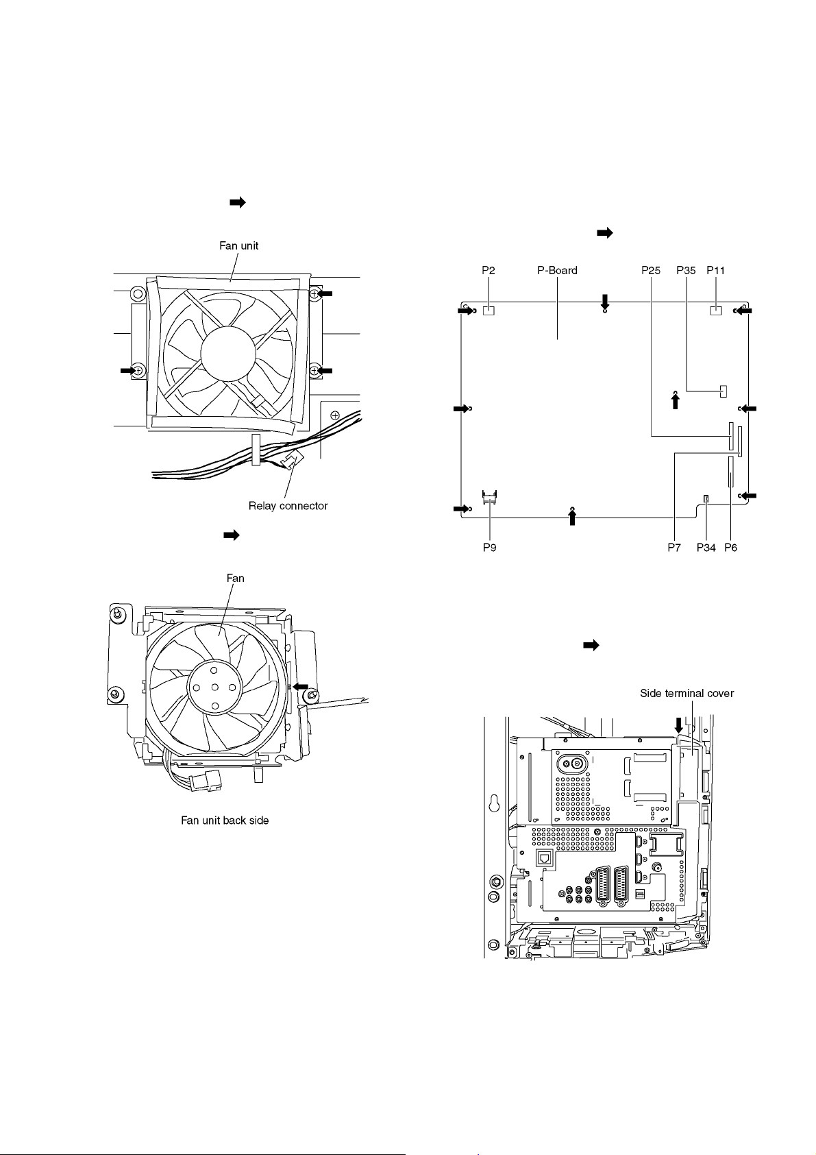
7.2. Remove the Fan
1. Unlock the cable clampers to free the cable.
2. Remove the screws (×3 ).
3. Remove the relay connectors and remove the Fan unit.
7.3. Remove the P-Board
Caution:
To remove P.C.B. wait 1 minute after power was off for discharge from electrolysis capacitors.
1. Unlock the cable clampers to free the cable
2. Disconnect the connectors (P2, P6, P7, P9, P11, P25,
P34 and P35).
3. Remove the screws (×9 ) and remove the P-Board.
4. Remove the screw (×1 ) on the back side.
5. Remove the Fan.
7.4. Remove the Side terminal cover and Rear terminal cover
1. Remove the claw (×1 ).
2. Remove the Side terminal cover.
19
3. Remove the Adjustment cover.
4. Remove the screws (×4 , ×4 , ×2 ).
5. Remove the Rear terminal cover.
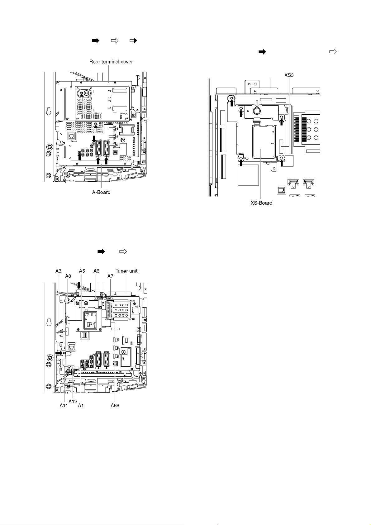
7.5. Remove the Tuner unit
1. Unlock the cable clampers to free the cable.
2. Disconnect the connectors (A1, A3, A5, A6, A7, A8, A11
and A12).
3. Disconnect the flexible cables (A88).
4. Remove the screws (×2 , ×1 ) and remove the
Tuner unit.
7.6. Remove the XS-Board
1. Disconnect the flexible cable (XS3).
2. Remove the screws (×5 ) and remove the nut (×1 ).
3. Remove the XS-Board.
20
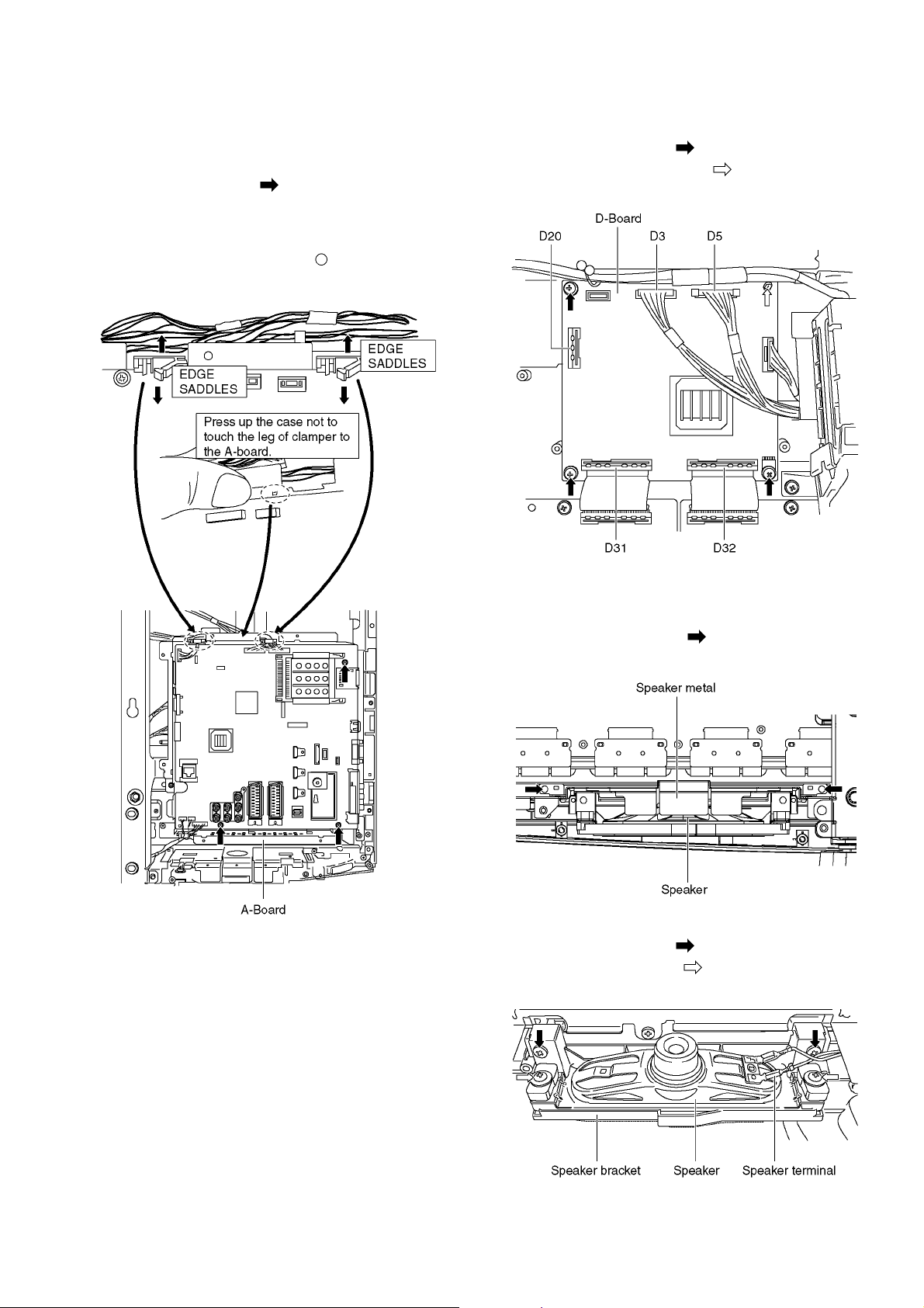
7.7. Remove the A-Board
1. Remove the Tuner unit (See section 7.5.)
2. Remove two EDGE SADDLES at top of case.
Twist the EDGE SADDLE to press up at the back and
pull down the front side.
3. Remove the screws (×3 ) and remove the A-Board.
Caution :
Press up the case not to touch the leg of clamper to the Aboard.
Pay attention two metal projection from back side when
removal and assemble.
7.8. Remove the D-Board
1. Disconnect the connectors. (D3 and D5)
2. Disconnect the flexible cables. (D20, D31 and D32)
3. Remove the screws (×3 ).
4. Remove the molding prop (×1 ).
5. Remove the D-Board.
7.9. Remove the Speakers
1. Unlock the cable clampers to free the cable.
2. Remove the screws (×2 ) and remove the Speaker
metals (L, R).
3. Disconnect the Speaker terminal.
4. Remove the screws (×2 ).
5. Remove the screws (×2 ) and remove the Speakers
(L, R) from the Speaker brackets (L, R).
21
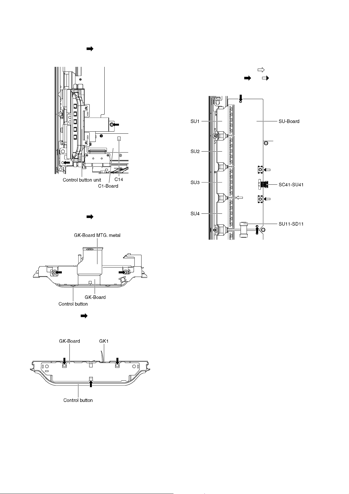
7.10. Remove the Control button unit
1. Disconnect the connector (C14).
2. Remove the screws (×2 ).
3. Remove the Control button unit.
7.11. Remove the GK-Board
1. Remove the Control button unit. (See section 7.10.)
2. Remove the screws (×2 ).
3. Remove the GK-Board MTG. metal.
7.12. Remove the SU-Board
1. Remove the flexible cables (SU1, SU2, SU3 and SU4)
connected to the SU-Board.
2. Remove the flexible cable (SU11-SD11) and the bridge
connector (SC41-SU41).
3. Remove the molding prop (×1 ).
4. Remove the screws (×2 , ×2 ) and remove the SU-
Board.
4. Remove the claw (×3 ).
5. Disconnect the connector (GK1).
6. Remove the GK-Board from Control button.
22
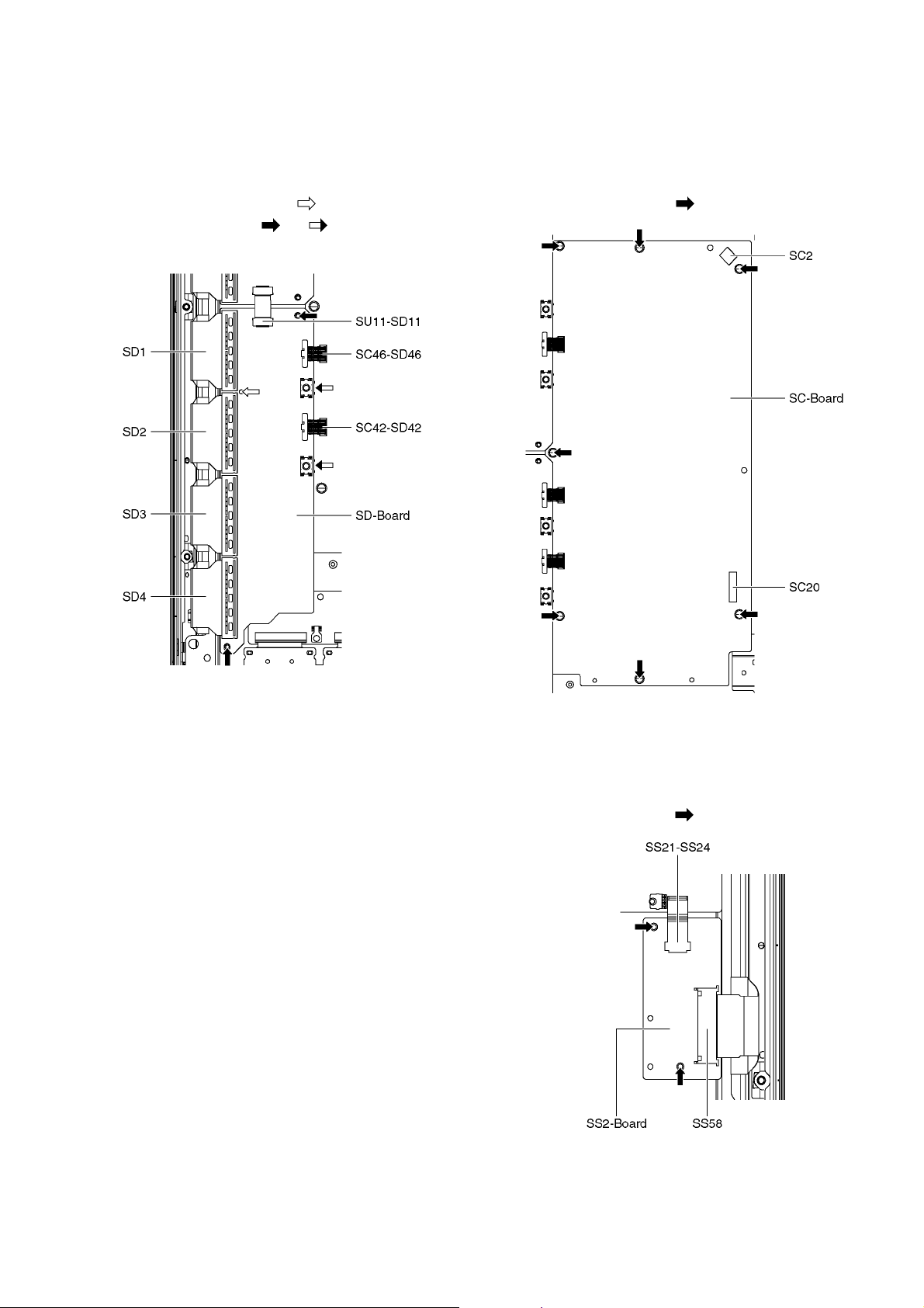
7.13. Remove the SD-Board
1. Remove the Control button unit. (See section 7.10.)
2. Remove the flexible cables (SD1, SD2, SD3 and SD4)
connected to the SD-Board.
3. Remove the flexible cable (SU11-SD11) and the bridge
connectors (SC42-SD42 and SC46-SD46).
4. Remove the molding prop (×1 ).
5. Remove the screws (×2 , ×2 ) and remove the SD-
Board.
7.14. Remove the SC-Board
1. Remove the SU-Board and SD-Board. (See section 7.12.
and 7.13.)
2. Unlock the cable clampers to free the cable.
3. Disconnect the connector (SC2).
4. Disconnect the flexible cable (SC20).
5. Remove the screws (×7 ) and remove the SC-Board.
7.15. Remove the SS2-Board
1. Remove the Tuner unit. (See section 7.5.)
2. Disconnect the bridge connector (SS21-SS24) and disconnect the flexible cable (SS58).
3. Remove the screws (×2 ) and remove the SS2-Board.
23
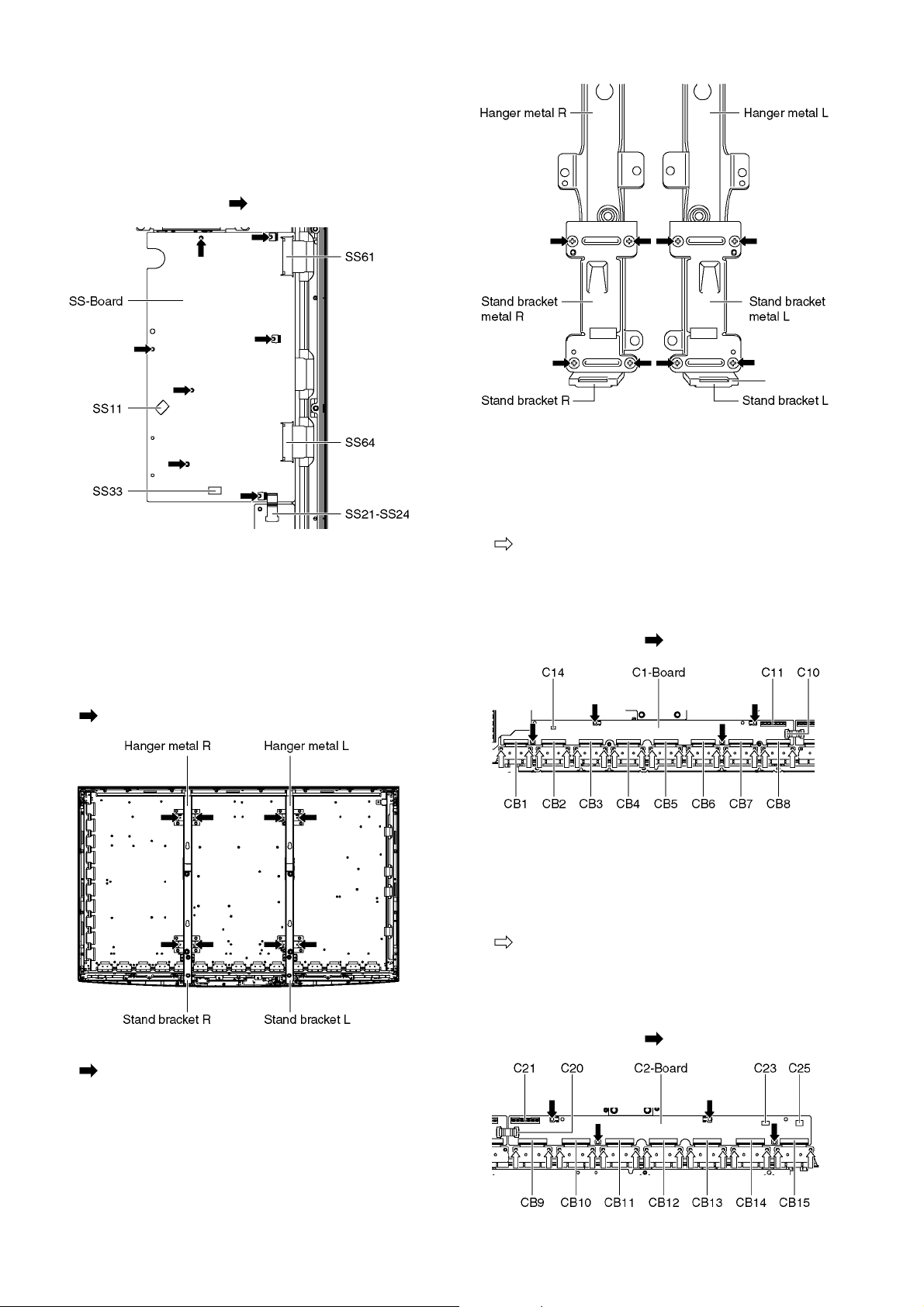
7.16. Remove the SS-Board
1. Remove the Tuner unit. (See section 7.5.)
2. Unlock the cable clampers to free the cable.
3. Disconnect the connectors (SS11 and SS33).
4. Disconnect the flexible cables (SS61 and SS64).
5. Disconnect the bridge connector (SS21-SS24).
6. Remove the screws (×7 ) and remove the SS-Board.
7.17. Remove the Hanger metals and the Stand brackets
1. Remove the Plasma panel section from the servicing
stand and lay on a flat surface such as a table (covered
by a soft cloth) with the Plasma panel surface facing
downward.
2. Remove the Hanger metals (L, R) fastening screws (×4
each) and remove the Hanger metals (L, R).
7.18. Remove the C1-Board
1. Remove the Control button unit. (See section 7.10.)
2. Remove the Hanger metal R and the Stand bracket R.
(See section 7.17.)
3. Remove the flexible cables holder fastening screws (×16
).
4. Disconnect the flexible cables (CB1, CB2, CB3, CB4,
CB5, CB6, CB7 and CB8).
5. Disconnect the connector (C14).
6. Disconnect the flexible cables (C10 and C11).
7. Remove the screws (×4 ) and remove the C1-Board.
3. Remove the Stand brackets (L, R) fastening screws (×4
each) and remove the Stand bracket metals (L, R)
and the Stand brackets (L, R).
7.19. Remove the C2-Board
1. Remove the Tuner unit. (See section 7.5.)
2. Remove the Hanger metal L and the Stand bracket L.
(See section 7.17.)
3. Remove the flexible cables holder fastening screws (×14
).
4. Disconnect the flexible cables (CB9, CB10, CB11, CB12,
CB13, CB14 and CB15).
5. Disconnect the flexible cables (C20 and C21).
6. Disconnect the connectors (C23 and C25).
7. Remove the screws (×4 ) and remove the C2-Board.
24
7.20. Remove the Plasma panel section from the Cabinet assy
(glass)
1. Remove the cabinet assy and the plasma panel fastening
screws (×2 ).
2. Remove the claw (×2 ).
3. Remove the Rear cover hook holders (L, R).
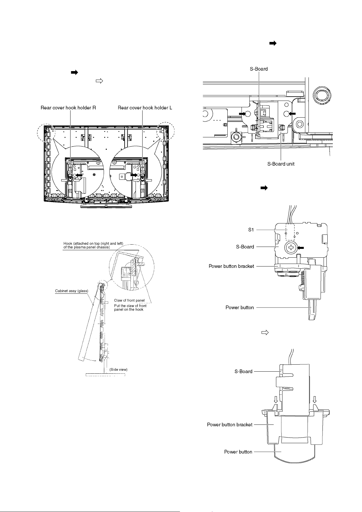
7.21. Remove the S-Board
1. Remove the screws (×2 ) and remove the S-Board
unit.
2. Disconnect the connector (S1).
3. Remove the screw (×1).
4. Remove the S-Board from the Power button bracket.
4. For leaving the plasma panel from the front frame, pull the
bottom of the cabinet assy forward, lift, and remove.
5. Remove the claws (×2 ).
6. Remove the Power button from the Power button bracket.
25
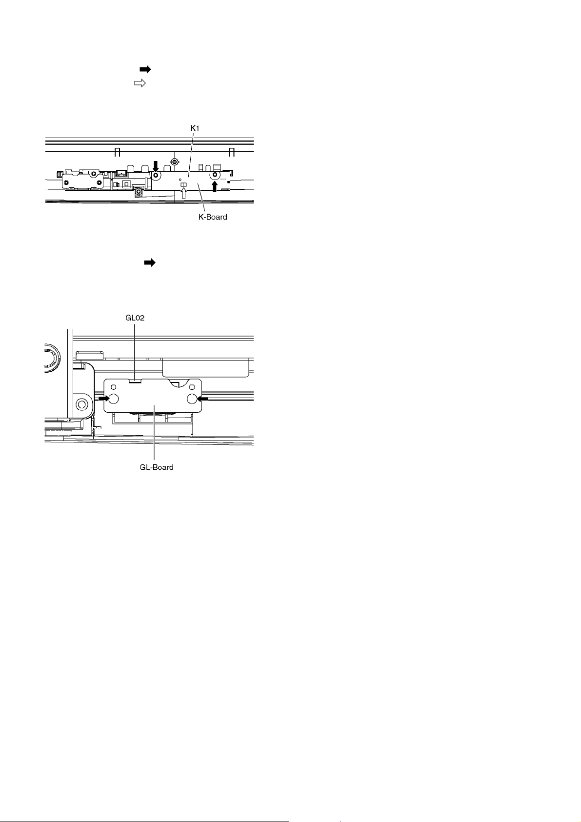
7.22. Remove the K-Board
1. Remove the screw (×2 ).
2. Remove the claw (×1 ).
3. Disconnect the connector (K1) and remove the K-Board
from LED Panel.
7.23. Remove the GL-Board
1. Remove the screws (×2 ).
2. Disconnect the connector (GL02) and remove the GLBoard.
7.24. Replace the plasma panel
Caution:
A new plasma panel itself without Hanger metals is
fragile.
To avoid the damage to new plasma panel, carry a new
plasma panel taking hold of the Hanger metals after
assembling the Hanger metals and the Stand brackets.
1. Place a carton box packed a new plasma panel on the flat
surface of the work bench.
2. Open a box and without taking a new plasma panel;
Attach the C1-Board and the C2-Board, connect the flexible cables from the plasma panel to the C1-Board and the
C2-Board, and fit the flexible cable holders.
3. Attach the Hanger metals and the Stand brackets to the
new plasma panel.
4. Place the plasma panel on the servicing stand taking hold
of the Hanger metals.
5. Attach the cabinet assy and each P.C.Board and so on, to
the new plasma panel.
*When fitting the cabinet assy, be careful not to allow any
debris, dust or handling residue to remain between the
front glass and plasma panel .
26
8 Measurements and Adjustments
8.1. Adjustment Procedure
8.1.1. Driver Set-up
8.1.1.1. Item / Preparation
1. Input a white signal to plasma video input.
2. Set the picture controls as follows.
Picture menu: Dynamic
PNR: Min
Aspect: 16:9
Caution
1. First perform Vsus adjustment.
2. The Vscn voltages are measured from the Vad (Vad_base), but may be measured from the GND (GND_base) in an
unavoidable case.
8.1.1.2. Adjustments
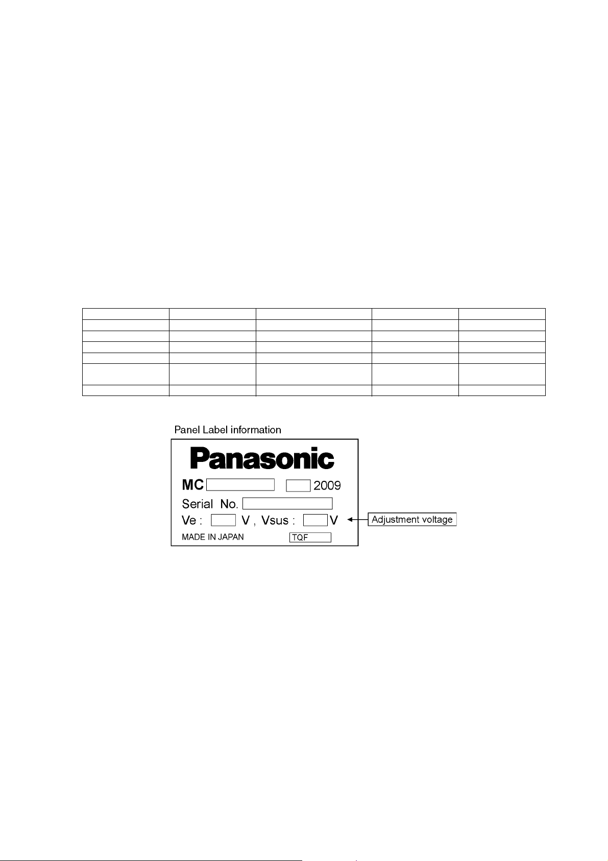
Adjust driver section voltages referring the panel data on the panel data label.
Check or adjust the following voltages with the multimeter.
Name Test Point Voltage Volume Remarks
Vsus TPVSUS (SS) Vsus ± 2V VR251(P) *
Ve TPVE (SS) Ve ± 2.5V Fixed *
Vset TPVSET (SC) 290V ± 9V Fixed
Vad TPVAD (SC) - 195V ± 2V VR16600 (SC)
Vscn TPVSCN (SC) Vad_base : 148V ± 1V
GND_base : - 47V ± 3V
Vda TP9 (P) 60V + 1V, - 2V Fixed
VR16841
(SC)
*See the Panel label.
27
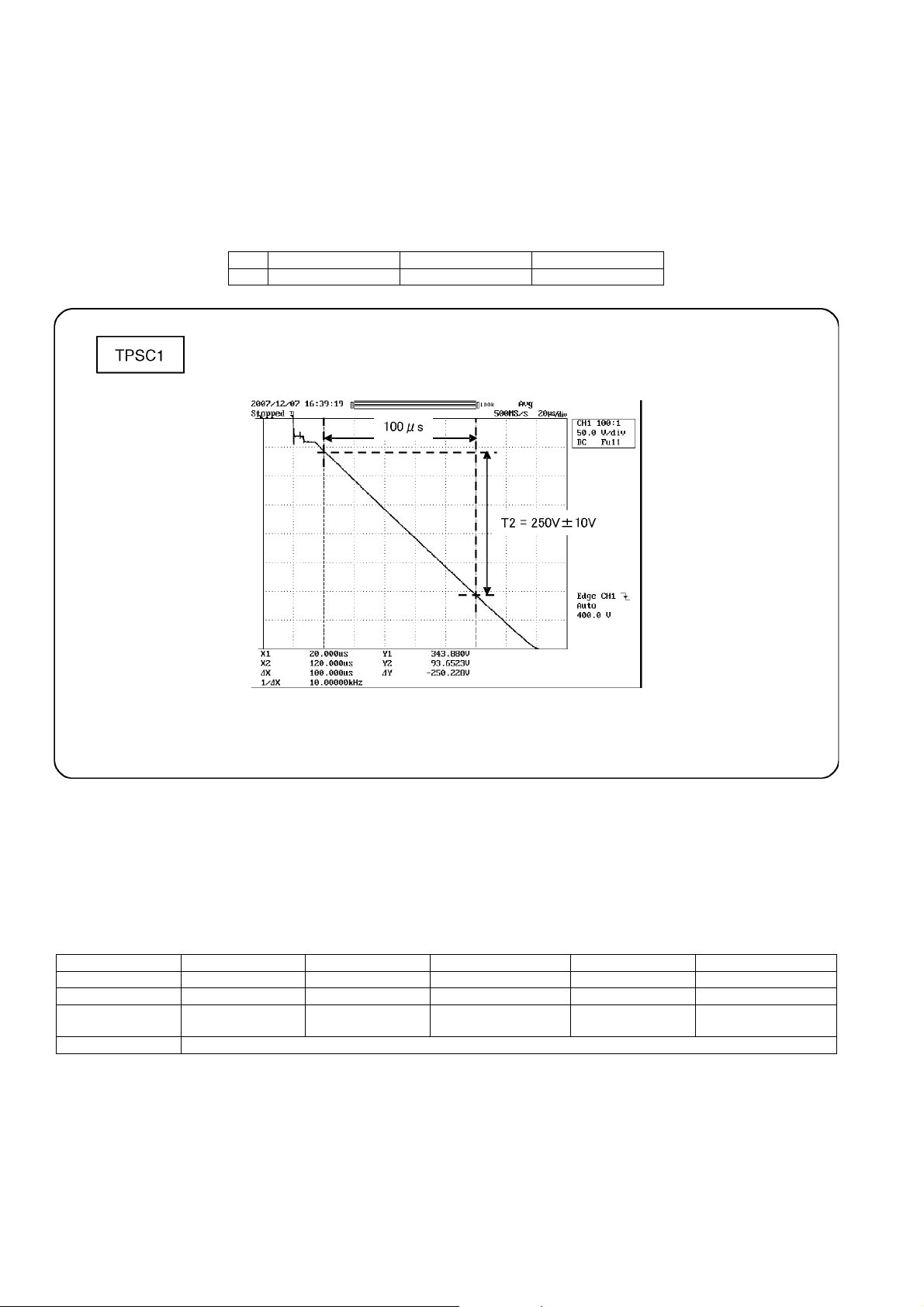
8.1.2. Initialization Pulse Adjust
1. Input the White signal to plasma video input.
2. Set the picture controls as follows.
Picture menu : Dynamic
PNR : Min
Aspect : 16:9
3. Connect Oscilloscope to TPSC1 (SC).
Check the voltage (T2) at 100μs period on the down slop.
Test point Volume Level
T2 TPSC1 (SC) VR16601 (SC) 250 V ± 10 V
8.1.3. P.C.B. (Printed Circuit Board) exchange
8.1.3.1. Caution
1. To remove P.C.B., wait 1 minute after power was off for discharge from electrolysis capacitors.
8.1.3.2. Quick adjustment after P.C.B. exchange
Adjust the following voltages with the multimeter.
P.C.B. Name Test Point Voltage Volume Remarks
P Board Vsus TPVSUS (SS) Vsus ± 2V VR251 (P) *
SC Board Vad TPVAD (SC) - 195V ± 2V VR16600 (SC)
SC Board Vscn TPVSCN (SC) Vad_base : 148V ± 1V
GND_base : - 47V ± 3V
A/D Board White balance and Sub brightness for NTSC, PAL, HD, PC and 625i signals
*See the Panel label.
Caution:
Absolutely do not reduce Vsus below Ve not to damage the P.C.B.
28
VR16841 (SC)
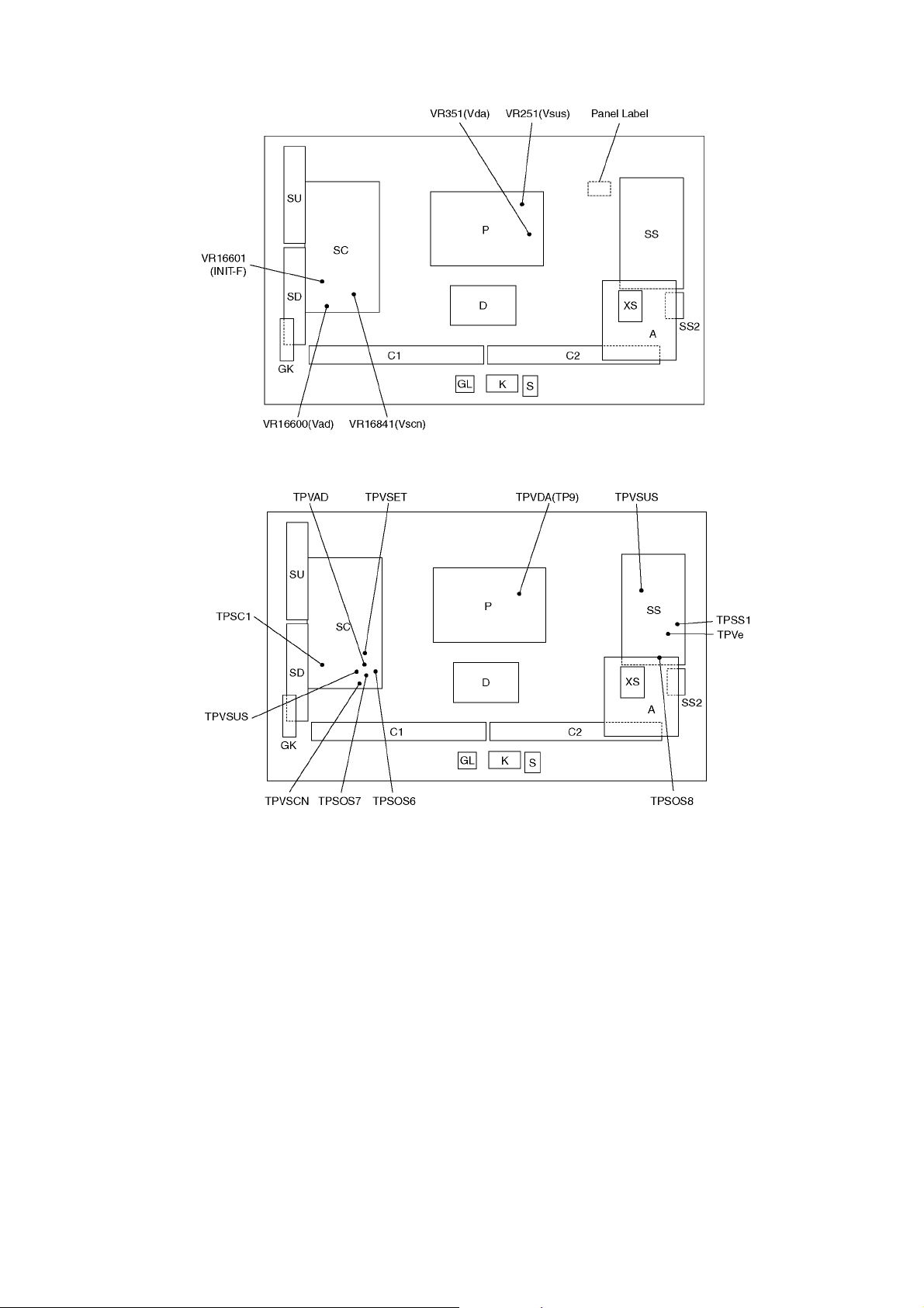
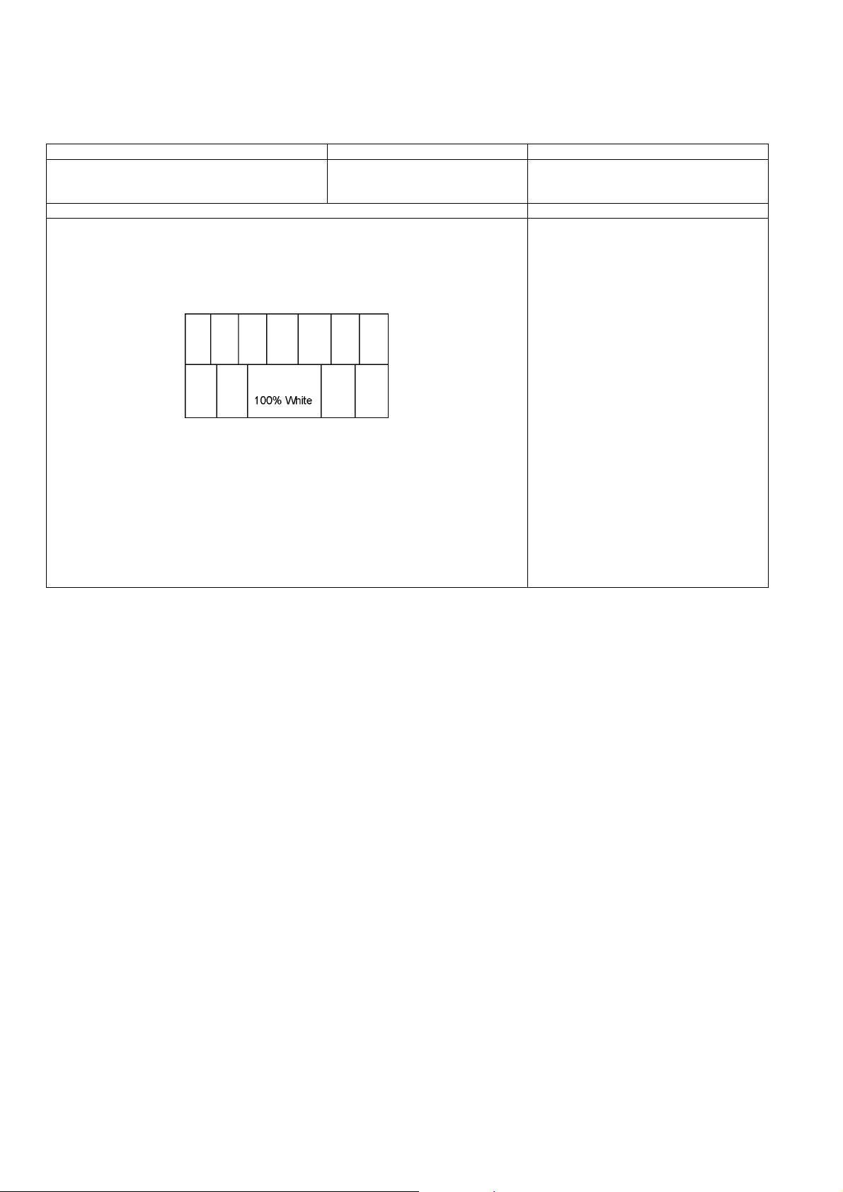
8.1.4. Adjustment Volume Location
8.1.5. Test Point Location
29
8.2. Adjustment
8.2.1. Sub-Contrast adjustment
Name of measuring instrument Connection Remarks
RF generator
Base Band signal generator
HD signal generator
Steps Remarks
Adjustment of TV (RF system)
Note:
In adjustment, you must setting to modulation of signal at 85%.
Ref.:
RF signal modulation spec.
UK models: 80%
Other models: 90%
1. Receive a RF PAL 100% Full White or Split Colour bar shown as below .
2. Goes into service adjustment mode.
3. Push a [ 1 ] or [ 2 ] key, and goes into adjustment mode for [ CONTRAST ].
Adjustment
1. The colour key yellow button of remote control is pushed.
2. The OSD character of sub-contrast becomes red.
(Inside under automatic adjustment)
3. The OSD character of sub-contrast returns to black.
4. End.
Note:
Sub-contrast adjustment is unadjusted
for AV/ HD input.
But, when needing the adjustment chosen manually, please refer to [ alternative method ].
30
 Loading...