

Page 1
ORDER No. PCZ0709120CE
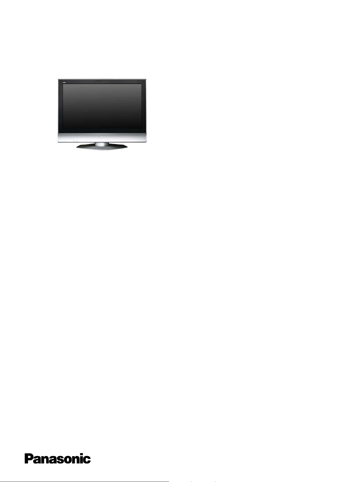
Service Manual
Colour LCD Television
TX-32LM70FA
TX-32LM70LA
TX-32LM70PA
TX-26LM70FA
TX-26LM70LA
TX-26LM70PA
TX-R32LM70A
TX-R26LM70A
GLP21MA Chassis
Specifications
(Information in brackets [ ] refers to model 26´´)
Power Source: 220-240V AC, 50Hz
Power Consumption: 121 [92W]
Stand-by Power
Consumption: 1W
Aerial Impedance: 75Ω unbalanced, Coaxial Type
Receiving System: PAL-B/G/I, D/K,
SECAM B/G, D/K, L/L’
PAL-525/60 (AV only)
M.NTSC (AV only)
NTSC (AV only)
Receiving Channels:
VHF E2-E12 VHF H1-H2 (ITALY)
VHF A-H (ITALY) VHF R1-R2
VHF R3-R5 VHF R6-R12
UHF E21-E69 CATV (S01-S05)
CATV S1-S10 (M1-M10) CATV S11-S20 (U1-U10)
CATV S21-S41 (Hyperband)
Operating Conditions:
Temperature: 5°C ÷ 35°C
Humidity: 5% ÷ 90% RH (non-condensing)
Intermediate Frequency:
Video/Audio
Video 38,9MHz, 33,9MHz
Audio 33,4MHz (B/G), 33,16MHz (A2)
33,05MHz (NICAM B/G, D/K, L)
32,4MHz (D/K), 32,66MHz (CZ STEREO)
40,4MHz (L’), 39,75MHz (L’NICAM),
32,35MHz,32,9MHz (NICAM)
Colour 34,47MHz (PAL)
34,5MHz, 34,65MHz (SECAM)
38,3MHz, 38,15MHz (SECAM L’)
Terminals:
AV1 IN Video (21 pin) 1V p-p 75Ω
Audio (21 pin) 500mV rms 10kΩ
RGB (21 pin) 0,7V p-p 75Ω
AV1 OUT Video (21 pin) 1V p-p 75Ω
Audio (21 pin) 500mV rms 1kΩ
AV2 IN Video (21 pin) 1V p-p 75Ω
Audio (21 pin) 500mV rms 10kΩ
RGB (21 pin) 0,7V p-p 75Ω
S-video IN Y: 1V p-p 75Ω
(21-pin) C:0,3V p-p 75Ω
AV2 OUT Video (21 pin) 1V p-p 75Ω
Audio (21 pin) 500mV rms 1kΩ
AV3 IN S-Video IN Y: 1V p-p 75Ω
(4-pin) C:0,3V p-p 75Ω
Video (RCAx1) 1V p-p 75Ω
HDMI1,HDMI2 Type A Connector
COMPONENT YUV Video (RCAx3) Y:1V p-p 75Ω
Pr:
Pb:
AUDIO IN Audio (RCAx2) 500mV rms 10kΩ
(for YUV, HDMI1)
AUDIO OUT Audio (RCAx2) 500mV rms 1kΩ
LCD screen: L5EDD8Q00036 [L5EDD6Q00027]
1366 x 768 XGA, 16:9
Visible Diagonal 800mm [660mm]
Audio Output: 2x10W RMS
8Ω impedance
Headphones: 3,5mm, 8Ω Impedance
Accessories
supplied : Remote Control
2 x R6 (UM3) Batteries
Dimensions:
Including TV stand 615mm 791mm 248mm
[525mm] [657mm] [216mm]
TV set only 563mm 791mm 107mm
[473mm] [657mm] [107mm]
Net weight: 16kg [12,5kg]
Specifications are subject to change without notice.
Weights and dimensions shown are approximate.
Audio (RCAx2) 500mV rms 10kΩ
±0,35V[ p-p] 75Ω
±0,35V[ p-p] 75Ω
Height: Width: Depth:
Page 2

Contents
SAFETY PRECAUTIONS........................................... 3
GENERAL GUIDE LINES...................................... 3
TOUCH – CURRENT CHECK............................... 3
PREVENTION OF ELECTROSTATIC DISCHARGE
(ESD) TO ELECTROSTATICALLY SENSITIVE (ES)
DEVICES.................................................................... 4
ABOUT LEAD FREE SOLDER (PBF)......................... 5
SUGGESTED PB FREE SOLDER........................ 5
SERVICE HINTS ........................................................ 6
CHASSIS BOARD LAYOUT....................................... 7
LOCATION OF LEAD WIRING................................... 7
SETTING INSPECTION.............................................. 8
SELF-CHECK ............................................................. 9
ADJUSTMENT METHOD ......................................... 10
WIRING DIAGRAM…………………………………….. 11
BLOCK DIAGRAMS.................................................. 12
PARTS LOCATION................................................... 15
REPLACEMENT PARTS LIST .................................. 16
SCHEMATIC DIAGRAMS......................................... 28
A-BOARD (1 OF 5) SCHEMATIC DIAGRAM ...... 29
A-BOARD (2 OF 5) SCHEMATIC DIAGRAM ...... 30
A-BOARD (3 OF 5) SCHEMATIC DIAGRAM ...... 31
A-BOARD (4 OF 5) SCHEMATIC DIAGRAM ...... 32
A-BOARD (5 OF 5) SCHEMATIC DIAGRAM ...... 33
B-BOARD SCHEMATIC DIAGRAM .................... 34
H-BOARD SCHEMATIC DIAGRAM .................... 35
K-BOARD SCHEMATIC DIAGRAM .................... 36
P-BOARD SCHEMATIC DIAGRAM .................... 37
V-BOARD SCHEMATIC DIAGRAM .................... 38
CONDUCTOR VIEWS .............................................. 39
2
Page 3
Safety Precautions
Ω
Ω
General Guide Lines
1. When servicing, observe the original lead dress. If a short circuit is found, replace all parts which have been overheated
or damaged by the short circuit.
2. After servicing, see to it that all the protective devices such as insulation barriers, insulation papers shields are properly
installed.
3. After servicing, make the following touch current checks to prevent the customer from being exposed to shock hazards.
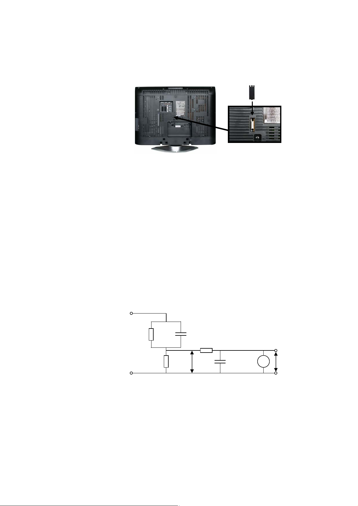
4. Always ensure panel TKP0E16001 is correctly replaced before returning to customer (see Fig.1).
Touch-Current Check
1. Plug the AC cord directly into the AC outlet. Do not use an isolation transformer for this check.
2. Connect a measuring network for touch currents between each exposed metallic part on the set and a good earth
ground such as a water pipe, as shown in Fig. 2.
3. Use Leakage Current Tester (Simpson 228 or equivalent) to measur e the potential across the measuring network.
4. Check each exposed metallic part, and measure the voltage at each point.
5. Reserve the AC plug in the AC outlet and repeat each of the above measure.
6. The potential at any point (TOUCH CURRENT) expressed as voltage U1 and U2, does not exceed the following values:
For a. c.: U1 = 35 V (peak) and U2 = 0.35 V (peak);
For d. c.: U1 = 1.0 V,
Note:
The limit value of U2 = 0.35 V (peak) for a. c. and U1 = 1.0 V for d. c. correspond to the values 0.7 mA (peak) a. c. and
2.0 mA d. c.
The limit value U1 = 35 V (peak) for a. c. correspond to the value 70 mA (peak) a. c. for frequencies greater than 100
kHz.
7. In case a measurement is out of the limits specified, there is a possibility of a shock hazard, and the equipment should
be repaired and rechecked before it is returned to the customer.
COLD
WATER PIPE
(EARTH GROUND)
Measuring network for TOUCH CURRENTS
TO
APPLIANCES
EXPOSED
METAL PARTS
Resistance values in ohms (Ω)
V: Voltmetr or oscilloscope
(r.m.s. or peak reading)
NOTE – Appropriate measures should be taken to obtain the correct value in case of non-sinusoidal waveforms
Input resistance: ≥ 1M
Input capacitance: ≤ 200pF
Frequency range: 15Hz to 1MHz and d.c.respectively
=1500Ω
R
S
Fig. 1
R0=500Ω
Fig. 2
C
S
=0.22μF
10k
U
1
0.022μF
V
U2 (V)
3
Page 4

Prevention of Electrostatic Discharge (ESD) to Electrostatically
Sensitive (ES) Devices
Some semiconductor (solid state) devices can be damaged easily by static electricity. Such components commonly are
called Electrostatically Sensitive (ES) Devices. Examples of typical ES devices are integr ated circuits and some field-effect
transistors and semiconductor "chip" components. The following techniques should be used to help reduce the incidence of
component damage caused by electrostatic discharge (ESD).
1. Immediately before handling any semiconductor component or semiconductor-equipped assembly, drain off any ESD on
your body by touching a known earth ground. Alternatively, obtain and wear a commercially available discharging ESD
wrist strap, which should be removed for potential shock reasons prior to applying power to the unit under test.
2. After removing an electrical assembly equipped with ES devices, place the assembly on a conductive surface such as
aluminum foil, to prevent electrostatic charge build up or exposure of the assembly.
3. Use only a grounded-tip soldering iron to solder or unsolder ES devices.
4. Use only an anti-static solder removal device. Some solder removal devices not classified as "anti-static (ESD
protected)" can generate electrical charge sufficient to damage ES devices.
5. Do not use freon-propelled chemicals. These can ge nerate electrical charges sufficient to damage ES devices.
6. Do not remove a replacement ES device from its protective package until immediately before you are ready to install it.
(Most replacement ES devices are packaged with leads electrically shorted together by cond uctive foam, aluminum foil
or comparable conductive material).
7. Immediately before removing the protective material from the leads of a replacement ES device, touch the protective
material to the chassis or circuit assembly into which the device will be installed.
Caution
Be sure no power is applied to the chassis or circuit, and observe all other safety precautions.
8. Minimize bodily motions when handling unpackaged replacement ES devices. (Otherwise harmless motion such as the
brushing together of your clothes fabric or the lifting of your foot from a carpeted floor can generate static electricity
(ESD) sufficient to damage an ES device).
There are special components used in this equipment which are important for safety.
These parts are marked by in schematic diagrams, exploded views and replacement parts list. It is essential that
these critical parts should be replaced with manufacturer’s specified parts to prevent shock, fire, or other hazards. Do
not modify the original design without permission of manufacturer.
IMPORTANT SAFETY NOTICE
4
Page 5
About lead free solder (PbF)
Note: Lead is listed as (Pb) in the periodic table of elements.
In the information below, Pb will refer to Lead solder, and PbF will refer to Lead Free Solder.
The Lead Free Solder used in our manufacturing process and discussed below is (Sn+Ag+Cu).
That is Tin (Sn), Silver (Ag) and Copper (Cu) although other types are available.
This model uses Pb Free solder in it’s manufacture due to environmental conservation issues. For service and repair work,
we’d suggest the use of Pb free solder as well, although Pb solder may be used.
PCBs manufactured using lead free solder will have the PbF within a leaf Symbol
stamped on the back of PCB.
Caution
• Pb free solder has a higher melting point than standard solder. Typically the melti ng point is 50 ~ 70 °F (30~40°C)
higher. Please use a high temperature soldering iron and set it to 700 ± 20 °F (370 ± 10 °C).
• Pb free solder will tend to splash when heated too high (about 1100 °F or 600 °C).
If you must use Pb solder, please completely remove all of the Pb free solder on the pins or solder area before
applying Pb solder. If this is not practical, be sure to heat the Pb free solder until it melts, before applying Pb solder.
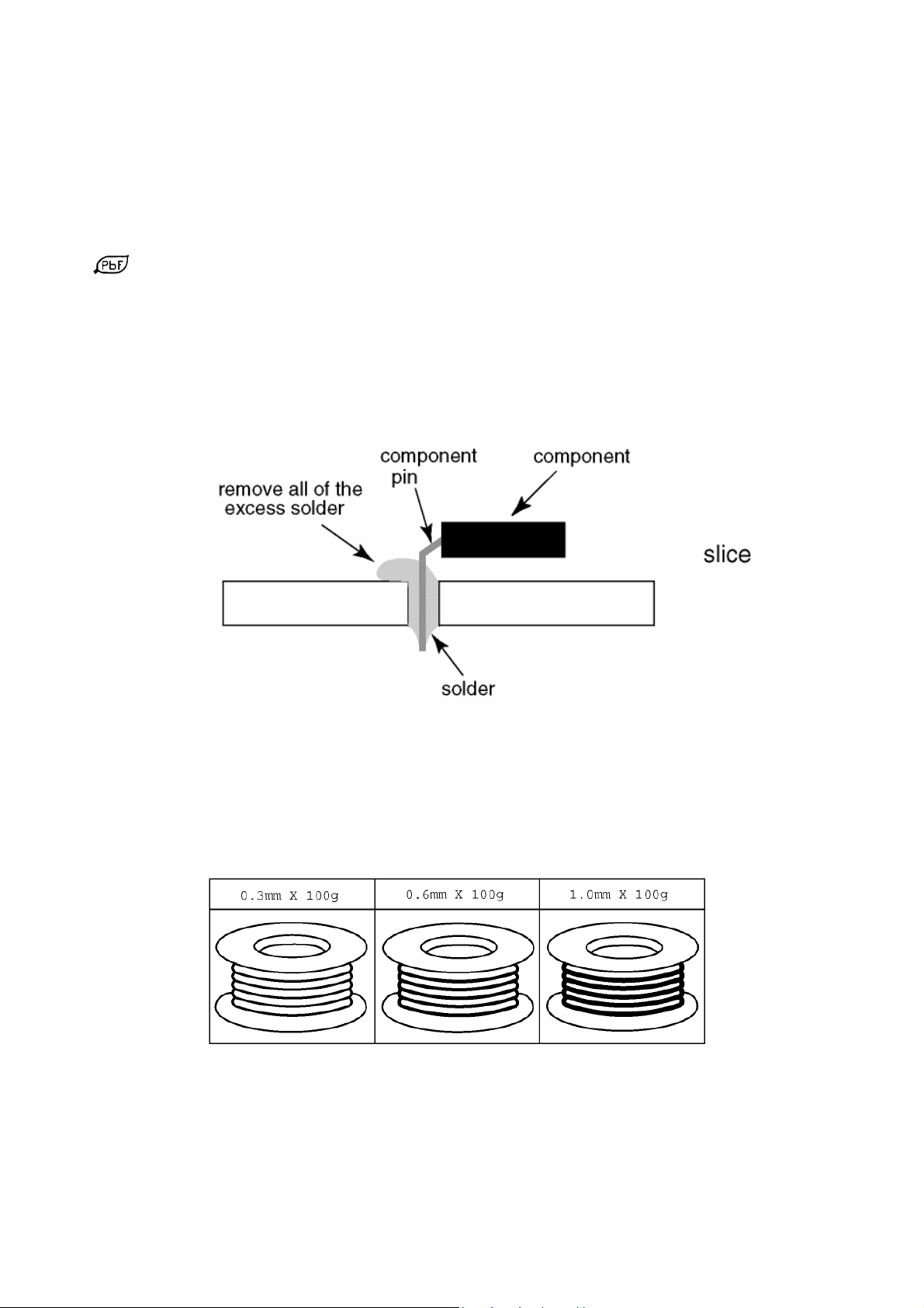
• After applying PbF solder to double layered boards, please check the component side for excess solder which may
flow onto the opposite side. (see Fig.3)
Suggested Pb free solder
There are several kinds of Pb free solder available for purchase. This product uses Sn+Ag+Cu (tin, silver, copper) solder.
However, Sn+Cu (tin, copper), Sn+Zn+Bi (tin, zinc, bismuth) solder can also be used. (see Fig.4)
Fig.3
Fig.4
5
Page 6
Service Hints
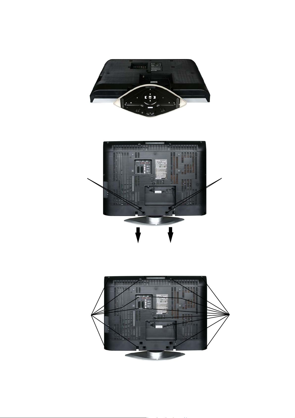
How to remove the Pedestal assembly
Lay the main unit face down. (see Fig.5)
Remove the 4 fixing screws and the pedestal assembly. (see Fig.6)
SCREWS
How to remove the backcover
Remove the 16[14] fixing screws. (see Fig.7)
SCREWS
Fig.5
Fig.6
Fig.7
SCREWS
SCREWS
6
Page 7
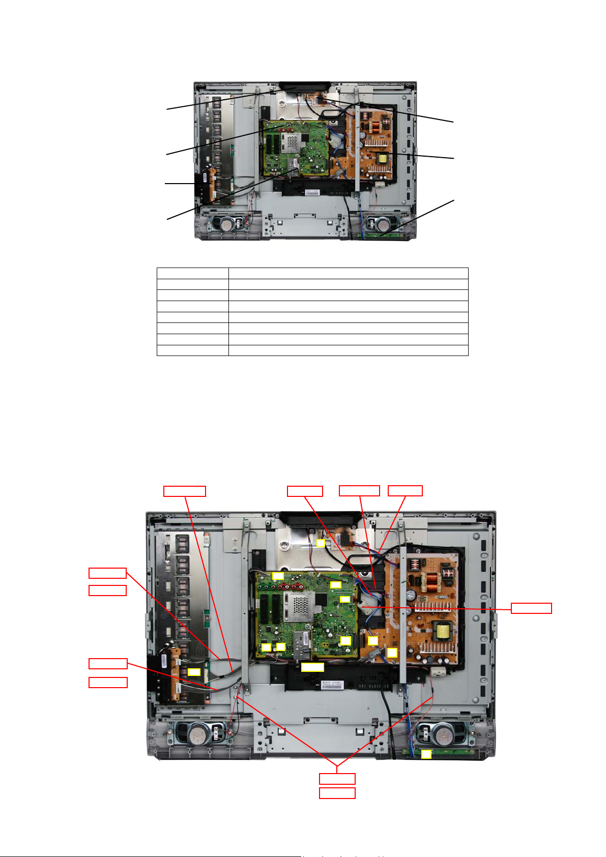
Chassis Board Layout
A8 –
A
A2–
A
A
A5–
A5–
KEY CONTROL
A-BOARD
H-BOARD
B-BOARD
Board Name Function
A-Board Main Board
B-Board Tuner
H-Board AV3 Terminal
Key Control Key Control
K-Board Mains Input, Power Switch
P-Board Power Supply
V-Board Remote Receiver, LED IR, Bats
Location of Lead Wiring
To find the Part Number of required wire in Replacement Parts List click on the wire name in red box.
[26”]
[26”]
A6 – H2
A6 – H2
A12 – H1
A12 – H1
P3 –PAN
CN1
V2
12
A6
A5
TU001
[26”]
K1
A13 –P4
10
2
A7
SP
SP
K3 –P1
P2
P3
V2
K-BOARD
P-BOARD
V-BOARD
PAN
7
Page 8

Setting Inspection
Voltage Confirmation
A board Normal mode
Test point Position Voltage Description
TP3800 Connector A7, pin 20
TP3806 Connector A7, pin 8
TP3810 Connector A7, pin 12
TP3811 Q3800, +pin
TP3802
TP3812 D3802, -pin
TP3801 IC3801, pin1
TP3805
TP3815 D3819, -pin
TP3813 C3801, pin
TP3804 C3808, +pin
TP3803 C3818, +pin
P board
TP833 Connector P2, pin 8
TP830 Connector P2, pin 9
TP832 Connector P2, pin 20
TP830 Connector P2, pin 12
TP833 Connector P2, pin 8
TP830 Connector P2, pin 9
Confirm the following voltages:
13,8V ± 0,7V STBY12V
23,9V±0,5V SIGNAL24V
23,9V ± 0,5V AUD24V
3,3V ± 0,3V 3.3V_HDMI
5,05V ± 0,25V 5V
8,2± 0,5V 8V
9V ± 0,9V 9V
13,8V ± 0,7V 12V
30V ± 2V 30V
Standby mode
5V ± 0,5V STBY5V
3,3V ± 0,2V STBY3.3V
1,8± 0,1V STBY1.8V
Normal mode
23,9V ± 0,5V SIGNAL24V
24,2V ± 0,5V AUD24V
13,8V ± 0,7V STBY12V
23,9V ± 0,5V AUD24V
Standby mode
24,2V± 0,5V SIGNAL24V
<10V AUD24V
8
Page 9
Self Check
CHEC
Self-check is used to automatically check the bus lines and hexadecimal code of the TV set. To enter Self-Check mode, keep
pressing the STATUS button on the remote control and press the down (-/v) button on the TV set. To exit Self Check,
switch off the TV set at the power button.
TX-32LM70FA
TX-32LM70PA
TX-26LM70LA
TX-R32LM70A
E2 O.K.
VCTP O.K.
AVSW O.K.
TUN O.K.
HDMI O.K.
Chassis 21
Model 01
Size 32
VCTP B3
E2 O.K.
VCTP O.K.
AVSW O.K.
TUN O.K.
HDMI O.K.
Chassis 21
Model 02
Size 32
VCTP B3
E2 O.K.
VCTP O.K.
AVSW O.K.
TUN O.K.
HDMI O.K.
Chassis 21
Model 08
Size 26
VCTP B3
E2 O.K.
VCTP O.K.
AVSW O.K.
TUN O.K.
HDMI O.K.
Chassis 21
Model 17
Size 32
VCTP B3
Panasonic 2007LCD
Self Check Complete
E2CRC 33
OPTION 1 0F
OPTION 2 00
OPTION 3 B9
OPTION 4 11
OPTION 5 00
OPTION 6 45
OPTION 7 FD
OPTION 8 D8
OPTION 9 00
OPTION 10 00
OPTION 11 13
OPTION 12 20
OPTION 13 1C
CHECK 42
Panasonic 2007LCD
Self Check Complete
E2CRC 61
OPTION 1 0F
OPTION 2 00
OPTION 3 B9
OPTION 4 11
OPTION 5 00
OPTION 6 45
OPTION 7 FD
OPTION 8 58
OPTION 9 00
OPTION 10 00
OPTION 11 13
OPTION 12 20
OPTION 13 1C
CHECK C2
Panasonic 2007LCD
Self Check Complete
E2CRC F1
OPTION 1 0D
OPTION 2 00
OPTION 3 39
OPTION 4 10
OPTION 5 00
OPTION 6 45
OPTION 7 3C
OPTION 8 58
OPTION 9 00
OPTION 10 40
OPTION 11 13
OPTION 12 48
OPTION 13 0C
CHECK D6
Panasonic 2007LCD
Self Check Complete
E2CRC A1
OPTION 1 0F
OPTION 2 00
OPTION 3 B9
OPTION 4 11
OPTION 5 00
OPTION 6 45
OPTION 7 FD
OPTION 8 58
OPTION 9 00
OPTION 10 00
OPTION 11 13
OPTION 12 20
OPTION 13 1C
CHECK C2
SW V1.12
E2 V02
TV V1.12
E2 V02
TV V1.12
E2 V02
TV V1.12
E2 V02
TX-32LM70LA
E2 O.K.
VCTP O.K.
AVSW O.K.
TUN O.K.
HDMI O.K.
Chassis 21
Model 04
Size 32
VCTP B3
TX-26LM70FA
E2 O.K.
VCTP O.K.
AVSW O.K.
TUN O.K.
HDMI O.K.
Chassis 21
Model 05
Size 26
VCTP B3
E2 O.K.
VCTP O.K.
AVSW O.K.
TUN O.K.
HDMI O.K.
Chassis 21
Model 06
Size 26
VCTP B3
TX-R26LM70A
E2 O.K.
VCTP O.K.
AVSW O.K.
TUN O.K.
HDMI O.K.
Chassis 21
Model 06
Size 26
VCTP B3
Panasonic 2007LCD
Self Check Complete
Panasonic 2007LCD
Self Check Complete
Panasonic 2007LCD
Self Check Complete
Panasonic 2007LCD
Self Check Complete
Display Ref. No. Description P.C.B.
E2 IC1120 EAROM A-Board
VCTP IC1501 AUDIO VIDEO TEXT PROCESSOR A-Board
AVSW IC1501 AV SWITCH A-Board
TUN TU001 TUNER B-Board
HDMI IC1503 HDMI A-Board
E2CRC A3
OPTION 1 0D
OPTION 2 00
OPTION 3 39
OPTION 4 10
OPTION 5 00
OPTION 6 45
OPTION 7 3C
OPTION 8 58
OPTION 9 00
OPTION 10 40
OPTION 11 13
OPTION 12 28
OPTION 13 0C
CHECK B6
E2CRC C3
OPTION 1 0F
OPTION 2 00
OPTION 3 B9
OPTION 4 11
OPTION 5 00
OPTION 6 45
OPTION 7 FD
OPTION 8 D8
OPTION 9 00
OPTION 10 00
OPTION 11 13
OPTION 12 40
OPTION 13 1C
K 62
E2CRC 00
OPTION 1 0F
OPTION 2 00
OPTION 3 B9
OPTION 4 11
OPTION 5 00
OPTION 6 45
OPTION 7 FD
OPTION 8 58
OPTION 9 00
OPTION 10 00
OPTION 11 13
OPTION 12 40
OPTION 13 1C
CHECK E2
E2CRC 94
OPTION 1 0F
OPTION 2 00
OPTION 3 B9
OPTION 4 11
OPTION 5 00
OPTION 6 45
OPTION 7 FD
OPTION 8 58
OPTION 9 00
OPTION 10 00
OPTION 11 13
OPTION 12 40
OPTION 13 1C
CHECK E2
SW V1.12
E2 V02
TV V1.12
E2 V02
TV V1.12
E2 V02
TV V1.12
E2 V02
If the CCU ports have been checked and found to be incorrect or not located then " - - " will appear in place of "O.K.".
9
Page 10
Adjustment Method
How to enter Service 1
• Set the Bass to maximum position, set the Treble to minimum position then keep pressing the INDEX button on the
remote control and press the down button (-/v) on the TV set, this will place the TV set into the Service Mode 1.
Key Command
• Press the RED / GREEN buttons to step up / down through the functions.
• Press the YELLOW / BLUE buttons to alter the function values, to alter White Rasters use +/- buttons
• Press the OK button after each adjustment has been made to store the required values.
• To exit the Service Mode, press the "N" button.
Keep adjusting sequence: DVCO, Sub-Contrast, other items.
Item
Sub-Contrast
DVCO
Highlight
Lowlight
Note: All setting values are approximate
High
Low 4 0064 0064 0064
Setting indication
Sub-Contrast
32
DVCO
63
12 0410 0410 0410
Settings / Special features
Receive a 80% white level Philips Pattern with correct
sound system (B/G, D/K) via aerial input. For Sub-
Contrast alignment press "Blue" button, wait until the
figure colour is changed from red to black colour.
Press the OK.
Receive a 80% white level Philips Pattern via aerial
input. For DVCO alignment press "Blue" button, wait
until the figure colour is changed from red to black
colour. Press the OK.
For correct setting see White Balance Adjustment
Sub-Brightness
White Balance Adjustment
Instrument
• Remote Control
• LCD WB meter (Minolta CA-210 or equivalent)
Condition
• Switch on the TV Set. Enter Service1. Step down to Highlight line and keep the aging time more than 20 minutes.
Procedure
• After aging time above set White Raster No.12 for Highlight and No.4 for Lo wlight Press the OK button
to store.
• Put Minolta Sensor to the center of the LCD Panel with 25mm gap between Minolta Sensor and LCD Panel. Adjust "x"
and "y" values by changing Red and Blue values.
• Press OK button to store setting.
Sub-Brightness
0
Item Value
Highlight
Lowlight
Optimum setting.
High 12
Low 4
x
y
x
y
2850±150
2940±150
2860±150
2900±150
10
Page 11
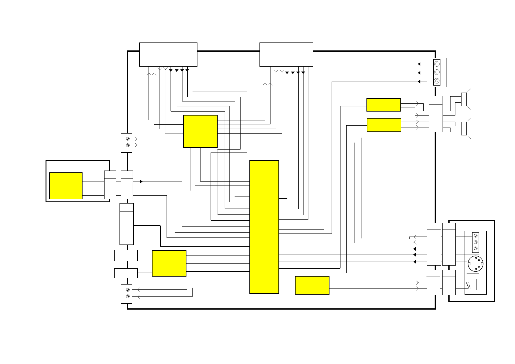
Wiring diagram
11
LCD-PANEL
B-BOARD
TNP0EA009
B1
P3
JK3000
AV1
JK3050
AV2
A2
A1
P-BOARD
TNP0EP009
P2
A7
A-BOARD
TNP0EA009
P1 K3
P4
A13
K-BOARD
TNP0EK009
MAINS IN
K1
A6 H2
A12 H1
JK3002
AUDIO IN
A8
JK3600
AV3
H-BOARD
TNP0EH009
V-BOARD
TNP0EV009
V2
B2
SERVICE
JK2300
AUDIO OUT
JK3001
YUV
JK5001
HDMI1
JK5000
HDMI2
A5 A5
SP-L
SP-R
A10
5 KEY BUTTON
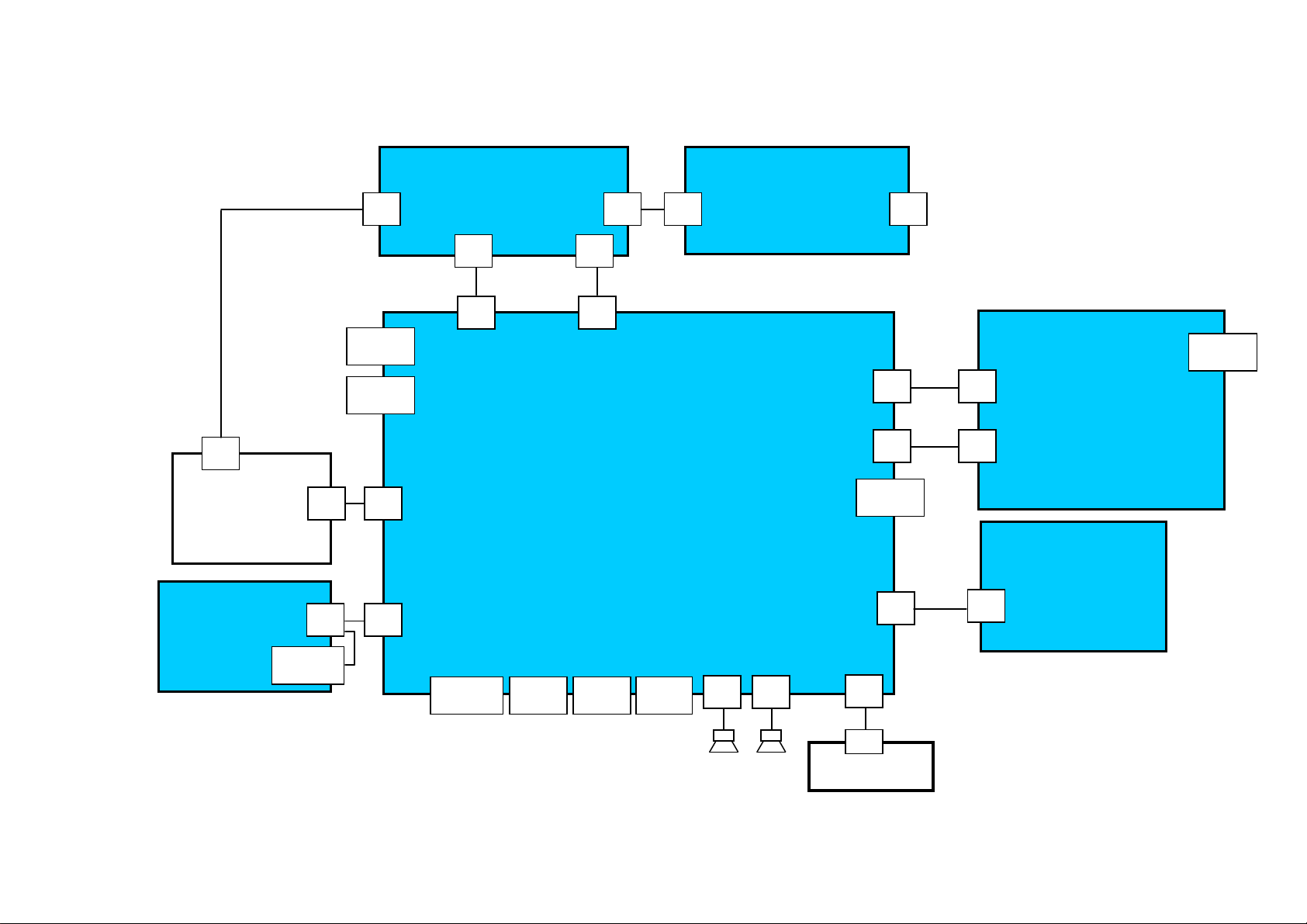
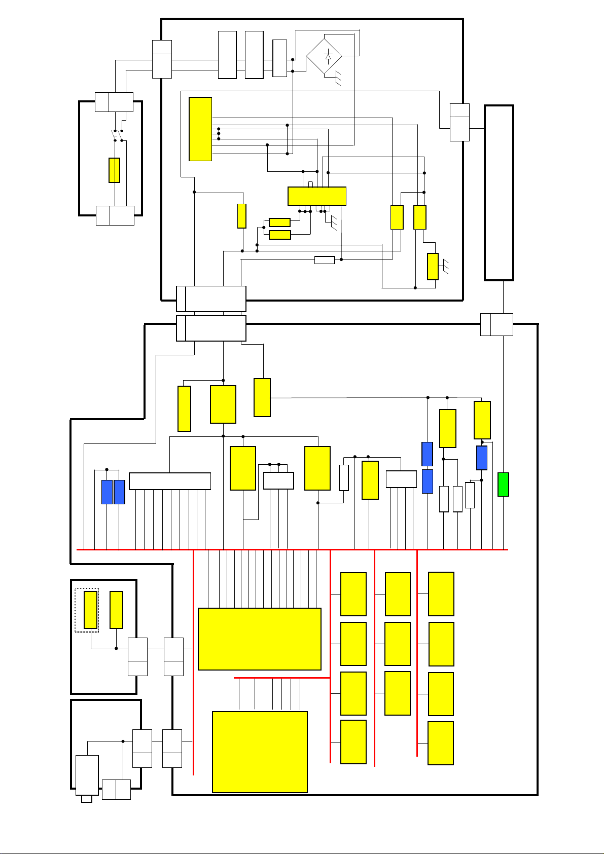
Page 12
A
V
Video & Stereo Audio Block Diagram
A
12
TUNER
TU001
ENGF7701GF
B-BOARD
TUNER CVBS
AM
B IN
7
G IN
11
CVBS OUT
RED/C IN
1520 19
A-BOARD
V
JK3001
AV1 21 PIN SCART
L OUT
R OUT
R IN
L IN
B IN
G IN
1 3 2 6 7 11 15 20
R IN
CVBS OUT
CVBS IN
19
AV2 21 PIN SCART
R OUT
1
L OUT
R IN
L IN
326
CVBS IN
U
Y
H1
8
6
4
1
3
H2
3
L
R
H-BOARD
C
Y
L
R
R
L
SP L
AV1 R OUT
33
AV1 L OUT
AV1 R IN
JK3002
AUDIO IN
R
L
B1
A1
13
11
10
13
11
10
SIF
AV1 L IN
YUV R IN
YUV L IN
IC3300
32
AUD_MATRIX
7
6
4
1 2 27 28
3
AV1 L OUT VCTP
A2
TO LCD PANEL
DATA TO PANEL
JK5001
8Bit data
HDMI
JK5000
HDMI
JK2300
R
L
8Bit data
IC5003
HDMI RECEIVER
MONITOR OUT R
MONITOR OUT L
AV1 R OUT VCTP
V1 AV2 AV3 YUV L IN AV1 AV2 AV3 YUV R IN
31
30
9
8
11
10
R 8Bit data Bus
G 8Bit data Bus
B 8Bit data Bus
MONITOR OUT R
MONITOR OUT L
AV1 R IN
AV1 G IN
AV1 B IN
AV1 CVBS IN
AV1 CVBS OUT
CVBS IN
50-57
58-65
66-73
SIF
AM
IC1501
VCT69XYP
9
10
23
24
178
177
176
189
195
191
31
13,14
21
22
190
179
180
181
194
174
172
173
184
187
188
28
27
26
25
V2 CVBS IN
AV2 B IN
AV2 G IN
AV2 RED/C IN
AV2 CVBS OUT
PR IN
PB IN
Y IN
AV3 CVBS IN
AV3 C IN
AV3 Y IN
SPEAKER L
SPEAKER R
HP L
3
HP R
5
IC270
HEDPHONE AMP
SP R
1
7
IC251
4
AUDIO AMP
IC252
4
AUDIO AMP
16
13
16
13
AV3 R IN
AV3 L IN
A5
4
3
2
1
A12
8
6
4
1
3
A6
1 3 1
Page 13
K-BOARD
,
,
,
,
,
,
,
C
3,3
,
,
,
,
,
,
,
,
,
,
_
K3
SW 800
F 800
K1
1
3
1
4
MAIN IN
P1
1
3
LINE
FILTER LF 800
IC800
7 9 5 3 2 4 1
MAIN PS CONTROL
Q830
L800
1 4 2
LINE
FILTER LF 802
D831
D832
~
3
~
D801
-
P3
1-5
1 2 3 4 7
T800
8
141516
9
13
12
10
11
PC801
PC800
LCD PANEL
P-BOARD
UD24 V
SIG24 V
STBY 12 V
P2
7
12
11
9
9,11,12
SIGNAL 24V
10
8
20-22
10
8
20-22
12V STBY
IC3800
PROTECTION
STBY 3.3V
SUPSIF 5V
VSUPAU 8V
18
33
IC1501
3V
SUPDIG 3
AUDIO VIDEO
36
3V
SUPDRI 3
PROCESSOR
STBY 1.8V
45,75
IC3801
VSUPIO1 3,3V
77
114
96
86
LCF´S
D5000
D5003
3V
SUPDRI 3,3V
SUPCOM 3,3V
SUPIO3 3
AUD24 V
5V MIXED P1
5V
5V MIXED P0
VSUPDIG 3,3V
SUPIO1 3,3V
Power Supply Block Diagram
BATS
6
STBY3.3V
V2
3V
SUPVO 3
6
A8
3V
3V
SUPFE 3
SUPDAC 3
3V
SUPLVDS 3
HDMI
3.3V
115
V-BOARD
1V8 HD
3V3 HD
B-BOARD
5V
TUNER
TU001
B2
5V
4
4
B1
A1
1
IC5003
HDMI RECEIVER
5,6,7,13,16,19,26,76,89,109
134
122
22,23,35,74,79,92,94,105,
114,128,139
12V
Q3802
LCF´S
SUPDIG 1.8V
SUPLVDS 1.8V
8V
SUPLVDS 1
VSUPLVDS 3,3V
124
142
127,133,139,150,156
3V3 PVCC
3V3 AVCC
37,55
38,42,46,50,57,61,65,69
SUPFE 1.8V
V
PDA
SUPFE 3,3V
VSUPFE 1,8V
185
170
164
169
3V3 REG
3V3 XTAL
99
98
SUPVO 3,3V
3V
SUPIO3 3
192
F830
Q3803
3.3V HDMI
197
5V
5V MIXED P1
5V MIXED P0
8V
LCF
3V3 HD
14,9,8,7
IC1380
8
IC5002
8
IC5001
8
IC1381
1V8 HD
DAC
EDID EPROM
EDID EPROM
OP AMP
LCF´S
IC5000
3V3 PVCC
8V
8
AUDIO 24V
18,5
UDIO 24V
18,5
3V3 XTAL
3V3 AVCC
HP AMP
IC270
IC252
AUDIO AMP
IC251
AUDIO AMP
IC 830
A2
26-30
PANEL 5V
IC3803
IC3802
D3807
D3806
LCF
5V
30V 12V
3V3 REG
STBY 3,3VSTBY 3,3V STBY 3,3V 9V
1,6
SWITCH
IC1220
8
EPROM
IC1120
2
RESET
IC1500
5
IC3300
AUD MATRIX
TUNER 5V
LCF
SUPAU 8V
D3802
Q1701
LCF
9V
8V
5V PANEL 5V
A-BOARD
13
Page 14

HDMI_SMUTE_INHIBIT
AMP Mute
HDMI_AUDIO_MUTE
HDMI_HP_MUTE
AUDIO _MUTE
POWER
SDA3,3V
SCL3,3V
12V
Q3801
Q3804
SUPPLY
STBY3.3V
IC1380
ENABLE 7
ENABLE 7
IC251
IC252
C1BB00000998
Q1721
C1BB00000998
Q1100
Q1101
LEVEL
SHIFTER
SCL 35
SDA 36
IC1220
C0JBAS000215
MULTIPLEXER
5
2
6,1
8
3
6 HDMI_MUTE
5 HDMI_SMUTE_INHIBIT
Q1380
16 FBL2
SCL_TUNER
HDMI_HPD_P1
HDMI_HPD_P1 166
92 HDMI_INT
SDA_TUNER
HDMI_HPD_P0
HDMI_HPD_P0 165
115 HDMI_RST
IC3300
KEYSCAN
KEYSCAN 162
116 HDMI_SMUTE_INHIBIT
159 AI_OFF
AV1 QLINK
AV2 QLINK
AV LINK OUT
AV LINK IN
AV1 IS QLINK
HCLK
HDMI_INT
AV1_SLOW
HDMI_RST
HDMI_SCDET
MUTE_OUT
HDMI_5V_DET_P1
HDMI_5V_DET_P0
5000
HDMI_5V_DET
MUTE_OUT
HDMI_MUTE
HDMI_SCDET
HDMI_AUDIO_MUTE
161
121
AV1_SLOW
HCLK
XTAL_IN 97
HDMI_RST 102
IC5003
SII9023CTU
HDMI RECEIVER
XTAL_OUT 96
HDMI_INT 104
HDMI_SCDET 103
33
MUTE_OUT 77
HDMI_5V_DET_P0 34
HDMI_5V_DET_P1
HDMI mute
5V
8V
30V
STBY3,3V
PROTECTION
3,3V_HDMI
EDID_WP_DISABLE
EEPROM_SDA 5
EAROM
IC1120
Q5011
7
IC5001
EDID_WP_DISABLE
C3EBFC000037
6 SCL_P0
5 SDA_P0
SCL_P0
SDA_P0
SCL 6
WR EN 7
Q5012
7
EDID_WP_DISABLE
5 SDA_P1
SDA_P1
IC5002
SCL_P1
160 AV2_SLOW
1 HDEN
3 HDVS
2 HDHS
27 SDA3,3V
Q5008
30 SCL3,3V_P1
31 SDA3,3V_P0
28 SCL3,3V
29 SDA3,3V_P1
Q5007
32 SCL3,3V_P0
SCL_P0
SDA_P0
Q5000
+5V_HDMI_P0
SCL_P1
SDA_P1
HPDT_5V_P0
Q5002
Q5001
HPDT_5V_P1
+5V_HDMI_P1
Q5003
Q5004
HP Mute
BACKLIGHT_PWM
PWM_OUT
STBY_LED
AUDIO_MUTE
BUS_REQUEST
Q1213
STBY_LED 208
AUDIO_MUTE 205
BUS_REQUEST 204
2 HDMI_5V_DET
1 IR
Q1212
HP_MUTE
HDMI_HP_MUTE
HDHS
SDA 3V3
IRD LED
AV_LINK_IN
AV2_FBL
V1 IS QLINK
AV_LINK_OUT
EDID_WP_DISABL
WR EN
AV1_FBL
BACKLIGHT_PWM
175
HDHS 171
SDA 3V3 203
IRD_LED 202
AV_LINK_IN 201
AV_LIN K_OUT 200
EDID_WP_DISABLE 199
IC1501
48 HDEN
47 HDVS
3 PANEL ON
7 PROTECTION
49 HCLK
83 SCL3,3V
AV1 IS QLINK 198
CT69XYP
AV2_FBL 183
VIDEO PROCESSOR
84 SDA3,3V
87 HDMI_CEC_OUT
88 HDMI_CEC_IN
WR EN 168
AV1_FBL
BACKLIGHT_PWM 167
89 NOT_STBY
91 INVERTER_OFF
90 INV_PSU_ON
Q1700
Q1207
Q1209
Q1217
Q3807
Q1701
HDMI_SMUTE_INHIBIT
C3EBFC000037
6 SCL_P1
Q5005
HDMI_MUTE
CEC
10 AV2_QLINK
8 AV2 SLOW
16 FBL1
10 AV1_QLINK
8 AV1_SLOW
13 CEC
15 SCL_P1
16 SDA_P1
18 +5V_HDMI_P1
19 HPDT_P1
13 CEC
15 SCL_P0
16 SDA_P0
18 +5V_HDMI_P0
19 HPDT_P0
AV2 21 PIN SCART
AV1 21 PIN SCART
HDMI2
HDMI1
Q1208
LCD PANEL 5V
HDEN
HDVS
HDMI_5V_DET
SDA_TUNER
9
9
SDA_TUNER
SCL_TUNER
8
8
33V
SCL_TUNER
PROTECTION
SCL3,3V
SDA3,3V
BUS_REQUEST
6
7
6
7
5V
SCL3,3V
SDA3,3V
BUS_REQUEST
IR
Control Block Diagram
A1
B1
HCLK
5
5
CEC_3,3V
SCL3,3V
SDA3,3V
A8
V2
NOT_STBY
INV_PSU_ON
INV_OFF
BATS
IRD_LED
STBY_LED
1
4
1
4
BATS
IRD_LED
STBY_LED
D1051
PC1060
14
13
TUNER
B - BOARD
B2
2
7
6
- BOARD
SERVICE
HDMI_INT
HDMI_RST
IR
2
2
IR
RM1050
HDHS
HDVS
BATS OFF
HDMI_SMUTE_INHIBIT
3
HDEN
AV2_SLOW
A10
3
SDA3,3V
SDA3,3V_P1
SCL3,3V_P1
SDA3,3V_P0
SCL3,3V
KEYSCAN
3
KEYSCAN
A7
P2
IRD_PSU_ON
23
23
23
Q834
INV_PSU_ON
Q831
ROUT
SCL3,3V_P0
1 1 3 2
Q832
PROTECTION
3 2 5
HDMI_HPD_P0
HDMI_5V_DET_P0
SDA_3,3V_P0
SCL_3,3V_P0
SDA_3,3V_P1
SCL_3,3V_P1
HDMI_5V_DET_P1
CEC_3,3V
HDMI_HPD_P1
A - BOARD
5
P3
PWM DIM
INVERTER ON
PANEL SOS
11 12 14
MATRIX
PC801
REMOTE
CONTROL
LOCAL KEYS SWITCHING
KEY CONTROL
B3PAA0000363
POWER SUPPLY
P - BOARD
POWER SUPPLY 24V
LCD PANEL
14
Page 15

Parts Location
The numbers on the exploded view below refer to the exploded view section of the Replacement Parts List.
NOTE:
3
20
5
28
4
26
25
16
22
(CONTINENTAL)
(UK)
27
6
19
17
15
12
7
13
30
[23]
18
11
9
21
24
2
[23]
8
29
1
14
10
15
Page 16

Replacement Parts List
Components Identified by mark have special characteristics important for safety.
In case of ordering these spare parts, please always add the complete Model-Type number to your order.
RTL (Retention Time Limited)
Note:
* When replacing any of these components, use only manufacturers specified parts.
The marking (RTL) indicates that the Retention Time is Limited for this item. After the
discontinuation of this assembly in production, the item will continue to be available for
a specific period of time. The retention period of availability is dependent on the type of
assembly, and in accordance with the laws governing part and product retention. After
the end of this period, the assembly will no longer be available.
Important Safety Notice
X
The marking (X) indicates that board should be exchanged for service.
DescriptionCct Ref Parts Number DescriptionCct Ref Parts Number
COMMON PARTS
EXPLODED VIEW
SPEAKER 1 EAS12S11F
TUNER 2 ENGF7701GF
REMOTE CONTROL 3 EUR7651030A
KEY BUTTON MODULE 4 K0RB00500013
PANASONIC BADGE 5 TBMA216-1
CONNECTOR COVER 6 TKP0E16001
WALL MOUNT METAL 7 TKZ0E9901
TUNER COVER 8 TMW0E107-2
CHASSIS FRAME 9 TMX0E410-2
B P.C.B. 10 TNP0EB009AA
H P.C.B. 11 TNP0EH009AA
K P.C.B. 12 TNP0EK009AA
P P.C.B. 13 TNP0EP009AC
V P.C.B. 14 TNP0EV009AA
POWER BUTTON ASSY 15 TTP0E0020
MISCELLANEOUS COMPONENTS
FERRITE CORE . J0KF00000018
FERRITE CORE . J0KG00000100
BATTERY . R6RC/2P
AV3 LABEL . TBM0E0703
REAR AV LABEL . TBM0E0885-1
IR WINDOW . TKP0E17904
WALL MOUNT BARRIER. TMK0E938-1
TAB-RELEASE CABLE. TMM8E18048
SCREW . XTB4+15JFJK
SCREW . XTV3+8JFJK
SCREW . XTW3+12TFJ
SCREW .XYN3+J8FJ
SCREW . XYN4+F10FJ
I.C.s
AUDIO AMPLIFIER IC251 C1BB00000998
AUDIO AMPLIFIER IC252 C1BB00000998
HEADPHONE AMPLIFIERIC270 C0AAZB000001
MAIN PS CONTROL IC800 C0DACLH00001
REGULATOR IC830 C0DBEMC00044
VOLTAGE DETECTING ICIC863 C0EBH0000298
LOGIC IC IC1220 C0JBAS000215
D/A CONVERTER IC1380 C0FBBK000047
OP-AMPLIFIER IC1381 BA15218FDXE2
I.C. RESET IC1500 C0EBE0000120
VCT IC IC1501 VCT6973B3A00
RTL
RTL
RTL
RTL
RTL
AUDIO SWITCH IC3300 AN15862A-VT
REGULATOR IC3800 C0DBAMH00018
1.8V REGULATOR IC3801 XC6365D105MR
5V REGULATOR IC3802 C0DBAJH00016
REGULATOR IC3803 C0DBAHC00034
1.8V REGULATOR IC5000 C0DBFFD00003
2KBIT EEPROM IC5001 C3EBDC000067
2KBIT EEPROM IC5002 C3EBDC000067
HDMI RECEIVER IC5003 C1AB00002848
PHOTO COUPLER PC800 B3PAA0000363
PHOTO COUPLER PC801 B3PAA0000363
PHOTO COUPLER PC1060 B3JB00000026
LED RECEIVER RM1050 PNA4701M05TV
FUSES
MICRO CHIP FUSE F100 ERBSE2R00U
AC FUSE F800 K5D502BNA007
FS LINK F830 K5G2523A0003
FS LINK F831 K5G2523A0003
DIODES
DIODE D270 MA22D3900L
DIODE D271 MA22D3900L
DIODE D272 1N4148WS
DIODE D273 MA22D3900L
DIODE D274 MA22D3900L
DIODE D275 1N4148WS
DIODE D301 1N4148WS
DIODE D800 B0HAGV000004
DIODE D803 B0HAGV000004
DIODE D804 B0HAMM000146
DIODE D805 B0EBNT000016
DIODE D808 05NU42TPA2Q
DIODE D809 B0HAGV000004
DIODE D810 B0BA01000069
DIODE D811 B0EAKT000019
DIODE D828 MA2160LFS
DIODE D830 B0HAKM000011
DIODE D831 YG868C10RF91
DIODE D832 YG868C10RF91
DIODE D833 B0ACCK000005
DIODE D835 B0ACCK000005
DIODE D836 B0ACCK000005
DIODE D837 B0ACCK000005
ZENER DIODE D838 B0BA02600018
DIODE D839 MA2160LFS
DIODE D840 B0JCPE000028
DIODE D841 B0JCPE000028
DIODE D1051 B3CKE0000007
DIODE D1062 UDZSTE178.2B
16
Page 17

D5032 B0ACCK000005
TRANSISTORS
DescriptionCct Ref Parts Number DescriptionCct Ref Parts Number
DIODE D1101 MA24D5000B
DIODE D1102 MA24D5000B
DIODE D1201 MA2J72800L
DIODE D1700 B0ACCK000005
DIODE D3800 USF5G49TE16Q
DIODE D3801 UDZSTE176.2B
DIODE D3802 1N4148WS
DIODE D3803 MA24D5000B
DIODE D3804 MAZ81500ML
DIODE D3805 MAZ81500ML
DIODE D3806 B0HCMM000014
DIODE D3807 B0HCMM000014
DIODE D3808 MA24D5000B
DIODE D3809 B0HCMM000014
DIODE D3810 MA24D5000B
DIODE D3811 MA22D3900L
DIODE D3812 B0ACCK000005
ZENER DIODE D3813 MAZ80510ML
DIODE D3816 UDZSTE176.2B
DIODE D3817 B0BC9R1A0006
DIODE D3818 B0ACCK000005
DIODE D3819 B0ACCK000005
DIODE D3820 B0ACCK000005
DIODE D3822 B0ACCK000005
DIODE D5000 MA22D3900L
DIODE D5001 B0ACCK000005
DIODE D5003 MA22D3900L
DIODE D5004 B0ACCK000005
DIODE D5006 MAZ30560ML
DIODE D5007 MAZ30560ML
VARISTOR D5010 EZJZ0V80008B
VARISTOR D5011 EZJZ0V80008B
VARISTOR D5012 EZJZ0V80008B
VARISTOR D5013 EZJZ0V80008B
VARISTOR D5016 EZJZ0V80008B
VARISTOR D5017 EZJZ0V80008B
VARISTOR D5018 EZJZ0V80008B
VARISTOR D5019 EZJZ0V80008B
VARISTOR D5020 EZJZ0V80008B
VARISTOR D5021 EZJZ0V80008B
VARISTOR D5022 EZJZ0V80008B
VARISTOR D5023 EZJZ0V80008B
VARISTOR D5024 EZJZ0V80008B
VARISTOR D5025 EZJZ0V80008B
VARISTOR D5026 EZJZ0V80008B
VARISTOR D5027 EZJZ0V80008B
VARISTOR D5028 EZJZ0V80008B
VARISTOR D5029 EZJZ0V80008B
VARISTOR D5030 EZJZ0V80008B
VARISTOR D5031 EZJZ0V80008B
DIODE
D
IODE D5033 B0ACCK000005
DIODE D5034 B0ACCK000005
DIODE D5035 B0ACCK000005
DIODE D5036 B0ACCK000005
DIODE D5037 B0ACCK000005
DIODE D5038 B0ACCK000005
TRANSISTOR Q122 BC847B
TRANSISTOR Q123 BC847B
TRANSISTOR Q250 BC847B
TRANSISTOR Q254 BC847B
TRANSISTOR Q270 BC857B
TRANSISTOR Q271 BC857B
TRANSISTOR Q272 BC857B
TRANSISTOR Q273 BC847B
TRANSISTOR Q274 BC847B
Q3803 B1DHDC000028
TRANSFORMERS
COILS
TRANSISTOR Q275 BC847B
TRANSISTOR Q276 BC847B
TRANSISTOR Q277 BC847B
TRANSISTOR Q801 BC847B
TRANSISTOR Q802 BC847B
TRANSISTOR Q830 B1CGRD000002
TRANSISTOR Q831 BC847B
TRANSISTOR Q832 BC847B
TRANSISTOR Q833 BC847B
TRANSISTOR Q834 BC847B
TRANSISTOR Q1100 2N7002T
TRANSISTOR Q1101 2N7002T
TRANSISTOR Q1207 2SC584500L
TRANSISTOR Q1208 2SC584500L
TRANSISTOR Q1209 2SC584500L
TRANSISTOR Q1212 BC847B
TRANSISTOR Q1213 BC857B
TRANSISTOR Q1214 BC857B
TRANSISTOR Q1217 BC847B
TRANSISTOR Q1221 BC847B
TRANSISTOR Q1222 BC847B
TRANSISTOR Q1229 BC847B
TRANSISTOR Q1230 BC847B
TRANSISTOR Q1231 BC847B
TRANSISTOR Q1232 BC847B
TRANSISTOR Q1380 BC847B
TRANSISTOR Q1700 BC847B
TRANSISTOR Q1701 B1DHED000013
TRANSISTOR Q1721 2N7002T
TRANSISTOR Q2301 BC857B
TRANSISTOR Q2302 BC857B
TRANSISTOR Q2303 BC857B
TRANSISTOR Q2304 BC847B
TRANSISTOR Q2305 BC847B
TRANSISTOR Q3201 BC857B
TRANSISTOR Q3202 BC857B
TRANSISTOR Q3204 BC847B
TRANSISTOR Q3205 BC847B
TRANSISTOR Q3800 2SD10300SL
TRANSISTOR Q3801 BC847B
TRANSISTOR Q3802 B1DHED000013
TRANSISTOR
RANSISTOR Q3804 BC847B
T
TRANSISTOR Q3805 B1DHCC000024
TRANSISTOR Q3806 2SD10300SL
TRANSISTOR Q3807 BC847B
TRANSISTOR Q3808 BC847B
TRANSISTOR Q3809 BC847B
TRANSISTOR Q3810 BC847B
TRANSISTOR Q3811 BC857B
TRANSISTOR Q3812 BC847B
TRANSISTOR Q5000 B1MBACA00008
TRANSISTOR Q5001 2SK122800L
TRANSISTOR Q5002 2N7002T
TRANSISTOR Q5003 B1MBACA00008
TRANSISTOR Q5004 2SK122800L
TRANSISTOR Q5005 2N7002T
TRANSISTOR Q5007 2N7002T
TRANSISTOR Q5008 2N7002T
TRANSISTOR Q5009 2SC584500L
TRANSISTOR Q5010 2SC584500L
TRANSISTOR Q5011 2SC584500L
TRANSISTOR Q5012 2SC584500L
TRANSFORMER T800 ETS42BJ1L6AD
COILL100 EXCELSA35T
17
Page 18

L5013 J0JCC0000166
FILTERS
CRYSTALS
DescriptionCct Ref Parts Number DescriptionCct Ref Parts Number
COIL L101 ELJFC2R2KFB
COIL L102 ELJFC2R2KFB
COIL TALL08T100KAL103 G0A100GA0013
COIL TALV35VB6R8JL121 G0C6R8JA0021
COIL L122 TALV35VB100K
COIL L201 G1C470MA0188
COIL L202 G1C470MA0188
COIL L250 J0JHC0000034
COIL L251 J0JHC0000034
COIL L252 J0JHC0000034
COIL L253 J0JHC0000034
PFC COIL L800 G0A553G00001
COILL801 EXCELSA39V
COILL802 EXCELSA39V
CHOKE COIL L830 ELC10D100E
COIL L831 G0C6R8MA0058
COILL832 EXCELSA39V
COILL833 EXCELSA39V
COIL L1100 ELJFC2R2KFB
COIL L1101 ELJFC2R2KFB
COIL BLM18PG121SN1DL1380 J0JHC0000045
COIL L1381 ELJPA1R0MF
COIL L1500 TALV35VB100K
COIL TALL08T100KAL1501 G0A100GA0013
COIL L1502 TALV35VB100K
COIL L1503 TALV35VB100K
COIL L1504 TALV35VB100K
COIL TALL08T100KAL1505 G0A100GA0013
COIL L1506 TALV35VB100K
COIL L1507 TALV35VB100K
COIL L1509 TALV35VB100K
COIL TALL08T100KAL1514 G0A100GA0013
COIL TALL08T100KAL1515 G0A100GA0013
COIL L1518 J0JHC0000078
COIL L1519 J0JHC0000078
COIL L1520 J0JHC0000078
COIL L3021 ELJFCR68KFB
COIL L3022 ELJFCR68KFB
COIL L3023 ELJFCR68KFB
COIL L3024 ELJFCR68KFB
COIL L3025 ELJFCR68KFB
COIL L3026 ELJFCR68KFB
INDUCTOR L3028 J0JCC0000241
COIL L3600 ELJFA6R8KFB
COIL L3601 ELJFA6R8KFB
COIL L3800 G0A220ZA0041
COIL L3801 ELL6SH100ME
COIL L3802 ELLATV6R8N
COIL L3803 J0JJC0000015
COIL L3804 J0JJC0000015
COIL BLM18PG121SN1DL5000 J0JHC0000045
COIL BLM18PG121SN1DL5001 J0JHC0000045
COIL BLM18PG121SN1DL5002 J0JHC0000045
COIL L5003 J0JHC0000034
COIL L5004 J0JHC0000034
COIL L5005 J0JHC0000034
COIL L5006 J0JHC0000034
COIL BLM18PG121SN1DL5007 J0JHC0000045
COIL BLM18PG121SN1DL5008 J0JHC0000045
COIL BLM18PG121SN1DL5010 J0JHC0000045
COIL BLM18PG121SN1DL5012 J0JHC0000045
COIL
LINE FILTER LF800 G0B253G00007
LINE FILTER LF802 G0B253G00007
CRYSTAL X1500 AI202504E
RESISTORS
ERJ3GEYJ105 0.1W 5% 1M Ω
CRYSTAL X5000 H0J283500018
SMDJA10 ERJ12Y0R00 - - 0 Ω
S.M.CARBJA90 ERJ6GEY0R00 0.1W - 0 Ω
SMDJSA276 ERJ3GEY0R00 0.1W - 0 Ω
SMDJSA330 ERJ3GEY0R00 0.1W - 0 Ω
S.M.CARBR104 ERJ6GEYJ101 0.1W 5% 100 Ω
S.M.CARBR105 ERJ6GEYJ101 0.1W 5% 100 Ω
S.M.CARBR106 ERJ6GEYJ101 0.1W 5% 100 Ω
SMDR121 ERJ3GEY0R00 0.1W - 0 Ω
SMDR123 ERJ3GEY0R00 0.1W - 0 Ω
S.M.CARBR124 ERJ6GEYJ223 0.1W 5% 22K Ω
SMDR125 ERJ3GEYJ103 0.1W 5% 10K Ω
SMDR126 ERJ3GEYJ272 0.1W 5% 2K7 Ω
SMDR129 ERJ3GEY0R00 0.1W - 0 Ω
SMDR130 ERJ3GEYJ332 0.1W 5% 3K3 Ω
SMDR131 ERJ3GEYJ681V 0.1W 5% 680 Ω
SMDR132 ERJ3GEYJ101 0.1W 5% 100 Ω
SMDR133 ERJ3GEYJ102 0.1W 5% 1K Ω
S.M.CARBR134 ERJ6GEY0R00 0.1W - 0 Ω
SMDR135 ERJ3GEYJ471 0.1W 5% 470 Ω
SMDR201 ERJ3GEYJ222 0.1W 5% 2K2 Ω
S.M.CARBR202 ERJ3GEYJ473V 0.1W 5% 47K Ω
SMDR203 ERJ3GEYJ105 0.1W 5% 1M Ω
SMDR204 ERJ3GEYJ102 0.1W 5% 1K Ω
S.M.CARBR205 ERJ3GEYJ392V 0.1W 5% 3K9 Ω
S.M.CARBR206 ERJ6GEY0R00 0.1W - 0 Ω
SMDR207 ERJ3GEYJ102 0.1W 5% 1K Ω
SMDR208 ERJ3GEYJ101 0.1W 5% 100 Ω
SMDR209 ERJ3GEYJ222 0.1W 5% 2K2 Ω
S.M.CARBR210 ERJ6GEYJ100 0.1W 5% 10 Ω
SMDR211 ERJ8GEYJ153 0.25W 5% 15K Ω
S.M.CARBR213 ERJ6GEYJ223 0.1W 5% 22K Ω
S.M.CARBR214 ERJ6GEYJ103 0.1W 5% 10K Ω
SMDR215 ERJ3GEYJ222 0.1W 5% 2K2 Ω
S.M.CARBR216 ERJ3GEYJ473V 0.1W 5% 47K
SMDR217
SMDR218 ERJ3GEYJ102 0.1W 5% 1K Ω
S.M.CARBR219 ERJ3GEYJ392V 0.1W 5% 3K9 Ω
S.M.CARBR220 ERJ6GEY0R00 0.1W - 0 Ω
SMDR221 ERJ3GEYJ102 0.1W 5% 1K Ω
SMDR222 ERJ3GEYJ101 0.1W 5% 100 Ω
SMDR223 ERJ3GEYJ222 0.1W 5% 2K2 Ω
S.M.CARBR224 ERJ6GEYJ100 0.1W 5% 10 Ω
SMDR225 ERJ8GEYJ153 0.25W 5% 15K Ω
S.M.CARBR228 ERJ6GEYJ473 0.1W 5% 47K Ω
S.M.CARBR229 ERJ6GEYJ473 0.1W 5% 47K Ω
S.M.CARBR241 ERJ6GEY0R00 0.1W - 0 Ω
S.M.CARBR242 ERJ6GEY0R00 0.1W - 0 Ω
S.M.CARBR243 ERJ6GEY0R00 0.1W - 0 Ω
S.M.CARBR244 ERJ6GEY0R00 0.1W - 0 Ω
SMDR246 ERJ3GEY0R00 0.1W - 0 Ω
SMDR250 ERJ3GEYJ103 0.1W 5% 10K Ω
SMDR251 ERJ3GEYJ103 0.1W 5% 10K Ω
SMDR252 ERJ3GEYJ103 0.1W 5% 10K Ω
S.M.CARBR254 ERJ3GEYJ473V 0.1W 5% 47K Ω
SMDR258 ERJ3GEY0R00 0.1W - 0 Ω
SMDR265 ERJ3GEYJ471 0.1W 5% 470 Ω
SMDR266 ERJ3GEYJ471 0.1W 5% 470 Ω
S.M.CARBR267 ERJ3GEYJ104V 0.1W 5% 100K Ω
S.M.CARBR268 ERJ3GEYJ104V 0.1W 5% 100K Ω
SMDR272 ERJ3GEYJ102 0.1W 5% 1K Ω
SMDR273 ERJ3GEYJ102 0.1W 5% 1K Ω
SMDR274 ERJ3GEYJ562 0.1W 5% 5K6 Ω
S.M.CARBR275 ERJ6GEYJ681 0.1W 5% 680 Ω
S.M.CARBR276 ERJ6GEYJ681 0.1W 5% 680 Ω
SMDR277 ERJ3GEYJ102 0.1W 5% 1K Ω
Ω
18
Page 19

DescriptionCct Ref Parts Number DescriptionCct Ref Parts Number
SMDR278 ERJ3GEYJ332 0.1W 5% 3K3 Ω
SMDR279 ERJ3GEYJ332 0.1W 5% 3K3 Ω
S.M.CARBR280 ERJ3GEYJ104V 0.1W 5% 100K Ω
S.M.CARBR281 ERJ3GEYJ104V 0.1W 5% 100K Ω
SMDR282 ERJ6RBD103V 0.1W 0.5 10K Ω
SMDR283 ERJ6RBD103V 0.1W 0.5 10K Ω
S.M.CARBR284 ERJ6GEYJ473 0.1W 5% 47K Ω
SMDR285 ERJ6RBD103V 0.1W 0.5 10K Ω
S.M.CARBR286 ERJ6GEYJ473 0.1W 5% 47K Ω
S.M.CARBR287 ERJ6GEYJ473 0.1W 5% 47K Ω
SMDR288 ERJ6RBD103V 0.1W 0.5 10K Ω
S.M.CARBR289 ERJ6GEYJ473 0.1W 5% 47K Ω
S.M.CARBR290 ERJ6GEYJ472 0.1W 5% 4K7 Ω
SMDR291 ERJ3GEYJ103 0.1W 5% 10K Ω
SMDR292 ERJ3GEYJ332 0.1W 5% 3K3 Ω
SMDR295 ERJ3GEYJ222 0.1W 5% 2K2 Ω
S.M.CARBR299 ERJ3GEYJ104V 0.1W 5% 100K Ω
SMDR303 ERJ3GEY0R00 0.1W - 0 Ω
CARBONR800 ERC12ZGK105V 0.5W 10% 1M Ω
CARBONR801 ERDS1FJ224T 0.5W 5% 220K Ω
CARBONR803 ERDS1FJ224T 0.5W 5% 220K Ω
S.M.CARBR804 ERJ6GEYJ222 0.1W 5% 2K2 Ω
S.M.CARBR808 ERJ6GEYJ563 0.1W 5% 56K Ω
S.M.CARBR809 ERJ6GEYJ103 0.1W 5% 10K Ω
S.M.CARBR810 ERJ6GEYJ102 0.1W 5% 1K Ω
SMDR813 ERJ6ENF1002 0.125 1% 10K Ω
SMDR814 ERJ6ENF1002 0.125 1% 10K Ω
CARBONR815 ERDS1TJ100 0.5W 5% 10 Ω
ANTI-PULR816 ERG1DJ244E 1W 5% 240K Ω
METALR817 ERG3FJ470 3W 5% 47 Ω
RESISTORR820 D0XB106J0003 1W 5% 10M Ω
S.M.CARBR821 ERJ6GEYJ273 0.1W 5% 27K Ω
S.M.CARBR833 ERJ6GEYJ103 0.1W 5% 10K Ω
S.M.CARBR834 ERJ6GEYJ103 0.1W 5% 10K Ω
S.M.CARBR837 ERJ6GEYJ102 0.1W 5% 1K Ω
S.M.CARBR838 ERJ6GEYJ104 0.1W 5% 100K Ω
S.M.CARBR839 ERJ6GEYJ104 0.1W 5% 100K Ω
S.M.CARBR840 ERJ6GEYJ274 0.1W 5% 270K Ω
S.M.CARBR841 ERJ6GEYJ274 0.1W 5% 270K Ω
S.M.CARBR842 ERJ6GEYJ682 0.1W 5% 6K8 Ω
S.M.CARBR843 ERJ6GEYJ472 0.1W 5% 4K7 Ω
SMDR844 ERJ6RBD822 0.1W 0.5 8K2 Ω
SMDR845 ERJ6RBD303 0.1W 0.5 30K Ω
SMDR846 ERJ6RBD432 0.1W 0.5 4K3 Ω
S.M.CARBR847 ERJ6GEYJ273 0.1W 5% 27K Ω
S.M.CARBR848 ERJ6GEYJ103 0.1W 5% 10K Ω
S.M.CARBR849 ERJ6GEYJ102 0.1W 5% 1K Ω
S.M.CARBR850 ERJ6GEYJ104 0.1W 5% 100K Ω
S.M.CARBR851 ERJ6GEYJ222 0.1W 5% 2K2 Ω
S.M.CARBR852 ERJ6GEYJ683 0.1W 5% 68K Ω
S.M.CARBR853 ERJ6GEYJ101 0.1W 5% 100 Ω
S.M.CARBR854 ERJ6GEYJ101 0.1W 5% 100 Ω
S.M.CARBR856 ERJ6GEYJ101 0.1W 5% 100 Ω
S.M.CARBR857 ERJ6GEYJ103 0.1W 5% 10K Ω
SMDR880 ERJ3GEYJ101 0.1W 5% 100 Ω
SMDR881 ERJ3GEY0R00 0.1W - 0 Ω
S.M.CARBR886 ERJ6GEYJ471 0.1W 5% 470 Ω
SMDR888 ERJ3GEYJ472 0.1W 5% 4K7 Ω
SMDR890 ERJ3GEY0R00 0.1W - 0 Ω
SMDR894 ERJ3GEY0R00 0.1W - 0 Ω
S.M.CARBR1055 ERJ6GEYJ103 0.1W 5% 10K Ω
S.M.CARBR1056 ERJ6GEYJ470 0.1W 5% 47 Ω
SMDR1061 ERJ3GEYJ101 0.1W 5% 100 Ω
S.M.CARBR1062 ERJ3GEYJ271V 0.1W 5% 270
S.M.CAR
BR1063 ERJ3GEYJ271V 0.1W 5% 270 Ω
SMDR1102 ERJ3GEYJ101 0.1W 5% 100 Ω
SMDR1103 ERJ3GEYJ472 0.1W 5% 4K7 Ω
SMDR1104 ERJ3GEYJ101 0.1W 5% 100 Ω
Ω
R1251 ERJ3GEYJ104V 0.1W 5% 100K Ω
ERJ3GEYJ683 0.1W 5% 68K Ω
ERJ3GEYJ203V 0.1W 5% 20K Ω
SMDR1105 ERJ3GEYJ472 0.1W 5% 4K7 Ω
SMDR1106 ERJ3GEYJ822 0.1W 5% 8K2 Ω
SMDR1107 ERJ3GEYJ822 0.1W 5% 8K2 Ω
SMDR1110 ERJ3GEY0R00 0.1W - 0 Ω
SMDR1111 ERJ3GEY0R00 0.1W - 0 Ω
SMDR1113 ERJ3GEY0R00 0.1W - 0 Ω
SMDR1120 ERJ3GEYJ101 0.1W 5% 100 Ω
SMDR1121 ERJ3GEYJ101 0.1W 5% 100 Ω
SMDR1122 ERJ3GEY0R00 0.1W - 0 Ω
S.M.CARBR1123 ERJ3GEYJ104V 0.1W 5% 100K Ω
S.M.CARBR1124 ERJ3GEYJ104V 0.1W 5% 100K Ω
SMDR1125 ERJ3GEY0R00 0.1W - 0 Ω
SMDR1126 ERJ3GEY0R00 0.1W - 0 Ω
SMDR1142 ERJ3GEYJ472 0.1W 5% 4K7 Ω
SMDR1143 ERJ3GEYJ101 0.1W 5% 100 Ω
SMDR1216 ERJ3GEYJ474 0.1W 5% 470K Ω
SMDR1220 ERJ3GEYJ103 0.1W 5% 10K Ω
SMDR1223 ERJ3GEYJ472 0.1W 5% 4K7 Ω
SMDR1224 ERJ3GEYJ472 0.1W 5% 4K7 Ω
SMDR1225 ERJ3GEYJ472 0.1W 5% 4K7 Ω
S.M.CARBR1233 ERJ3GEYJ473V 0.1W 5% 47K Ω
SMDR1234 ERJ3GEYJ472 0.1W 5% 4K7 Ω
SMDR1235 ERJ3GEYJ273 0.1W 5% 27K Ω
S.M.CARBR1236 ERJ6GEYJ472 0.1W 5% 4K7 Ω
S.M.CARBR1237 ERJ6GEYJ472 0.1W 5% 4K7 Ω
S.M.CARBR1238 ERJ3GEYJ224V 0.1W 5% 220K Ω
S.M.CARBR1239 ERJ3GEYJ104V 0.1W 5% 100K Ω
SMDR1249 ERJ3GEYJ225 0.1W 5% 2M2 Ω
SMDR1250 ERJ3GEYJ333V 0.1W 5% 33K Ω
S.M.CARB
SMDR1252
S.M.CARBR1256 ERJ3GEYJ104V 0.1W 5% 100K Ω
S.M.CARBR1257 ERJ3GEYJ223V 0.1W 5% 22K Ω
SMDR1263 ERJ3GEYJ472 0.1W 5% 4K7 Ω
S.M.CARBR1264 ERJ3GEYJ473V 0.1W 5% 47K Ω
SMDR1265 ERJ3GEYJ225 0.1W 5% 2M2 Ω
S.M.CARBR1266 ERJ3GEYJ104V 0.1W 5% 100K Ω
S.M.CARBR1267 ERJ3GEYJ224V 0.1W 5% 220K Ω
SMDR1268 ERJ3EKF2702V 0.1W 1% 27K Ω
S.M.CARBR1269 ERJ3GEYJ104V 0.1W 5% 100K Ω
SMDR1270 ERJ3GEYJ221 0.1W 5% 220 Ω
S.M.CARBR1271 ERJ3GEYJ223V 0.1W 5% 22K Ω
SMDR1272 ERJ3GEY0R00 0.1W - 0 Ω
S.M.CARBR1295 ERJ3GEYJ104V 0.1W 5% 100K Ω
S.M.CARBR1296 ERJ3GEYJ104V 0.1W 5% 100K Ω
SMDR1297 ERJ3GEYJ334 0.1W 5% 330K Ω
SMDR1298 ERJ3GEYJ103 0.1W 5% 10K Ω
S.M.CARBR1299 ERJ3GEYJ563V 0.1W 5% 56K Ω
S.M.CARBR1301 ERJ3GEYJ563V 0.1W 5% 56K Ω
SMDR1302 ERJ3GEYJ561 0.1W 5% 560 Ω
SMDR1303 ERJ3GEYJ331 0.1W 5% 330 Ω
SMDR1304 ERJ3GEYJ472 0.1W 5% 4K7 Ω
SMDR1305 ERJ3GEYJ472 0.1W 5% 4K7 Ω
SMDR1377 ERJ2GEJ330X .063W 5% 33 Ω
SMDR1378 ERJ2GEJ330X .063W 5% 33 Ω
SMDR1379 ERJ2GEJ330X .063W 5% 33 Ω
S.M.CARBR1380 ERJ6GEYJ102 0.1W 5% 1K Ω
S.M.CARBR1381 ERJ6GEYJ103 0.1W 5% 10K Ω
SMDR1382 ERJ2GE0R00X .063W - 0 Ω
SMDR1383 ERJ2GEJ473X .063W 5% 47K Ω
SMDR1384 ERJ2GEJ473X .063W 5% 47K Ω
SMDR1385 ERJ2GEJ103X .063W 5% 10K Ω
SMDR1386 ERJ2GEJ103X .063W 5% 10K Ω
SMDR1387
SMDR1388 ERJ3GEYJ333V 0.1W 5% 33K Ω
SMDR1389 ERJ3GEYJ203V 0.1W 5% 20K Ω
S.M.CARBR1390 ERJ3GEYJ223V 0.1W 5% 22K Ω
SMDR1391 ERJ3GEYJ333V 0.1W 5% 33K Ω
19
Page 20

DescriptionCct Ref Parts Number DescriptionCct Ref Parts Number
S.M.CARBR1392 ERJ3GEYJ223V 0.1W 5% 22K Ω
SMDR1393 ERJ2GEJ102X .063W 5% 1K Ω
SMDR1395 ERJ2GEJ102X .063W 5% 1K Ω
SMDR1397 ERJ2GEJ101X .063W 5% 100 Ω
SMDR1398 ERJ2GEJ101X .063W 5% 100 Ω
SMDR1500 ERJ3GEYJ101 0.1W 5% 100 Ω
SMDR1501 ERJ8GEYJ750 0.25W 5% 75 Ω
S.M.CARBR1502 ERJ6GEYJ750 0.1W 5% 75 Ω
SMDR1503 ERJ3GEYJ101 0.1W 5% 100 Ω
SMDR1504 ERJ3GEYJ101 0.1W 5% 100 Ω
SMDR1505 ERJ3GEYJ123 0.1W 5% 12K Ω
SMDR1506 ERJ3GEYJ123 0.1W 5% 12K Ω
SMDR1507 ERJ8GEYJ750 0.25W 5% 75 Ω
SMDR1509 ERJ3GEYJ750 0.1W 5% 75 Ω
SMDR1510 ERJ3GEYJ750 0.1W 5% 75 Ω
S.M.CARBR1512 ERJ6GEYJ750 0.1W 5% 75 Ω
SMDR1513 ERJ3GEYJ302V 0.1W 5% 3K Ω
S.M.CARBR1514 ERJ6GEYJ750 0.1W 5% 75 Ω
SMDR1515 ERJ3GEYJ302V 0.1W 5% 3K Ω
SMDR1516 ERJ3GEYJ101 0.1W 5% 100 Ω
SMDR1517 ERJ3GEYJ101 0.1W 5% 100 Ω
S.M.CARBR1518 ERJ6GEYJ750 0.1W 5% 75 Ω
SMDR1521 EXB2HV101JV .063W 5% 100 Ω
SMDR1526 ERJ3GEYJ750 0.1W 5% 75 Ω
SMDR1527 ERJ3GEYJ750 0.1W 5% 75 Ω
S.M.CARBR1528 ERJ6GEYJ750 0.1W 5% 75 Ω
SMDR1529 ERJ3GEYJ101 0.1W 5% 100 Ω
SMDR1530 ERJ3GEYJ273 0.1W 5% 27K Ω
S.M.CARBR1531 ERJ6GEYJ750 0.1W 5% 75 Ω
S.M.CARBR1532 ERJ6GEYJ750 0.1W 5% 75 Ω
SMDR1533 ERJ3GEYJ101 0.1W 5% 100 Ω
SMDR1536 ERJ3GEY0R00 0.1W - 0 Ω
SMDR1537 ERJ3GEYJ101 0.1W 5% 100 Ω
CHIP RESR1540 EXB38V101JV .063W 5% 100
EXB2HV101JV .063W 5% 100 Ω
R1767 EXB24VR000X 0W - 0 Ω
SMDR1541
SMDR1542 ERJ3GEYJ472 0.1W 5% 4K7 Ω
SMDR1544 ERJ3GEYJ472 0.1W 5% 4K7 Ω
SMDR1545 ERJ3GEYJ101 0.1W 5% 100 Ω
SMDR1546 ERJ3GEYJ101 0.1W 5% 100 Ω
SMDR1548 ERJ2GEJ101X .063W 5% 100 Ω
S.M.CARBR1549 ERJ6GEYJ622 0.1W 5% 6K2 Ω
SMDR1550 EXB2HV101JV .063W 5% 100 Ω
SMDR1556 EXB2HV101JV .063W 5% 100 Ω
SMDR1568 ERJ3GEYJ101 0.1W 5% 100 Ω
SMDR1569 ERJ3GEYJ101 0.1W 5% 100 Ω
SMDR1579 ERJ3GEYJ103 0.1W 5% 10K Ω
SMDR1580 ERJ3GEYJ103 0.1W 5% 10K Ω
SMDR1585 ERJ3GEY0R00 0.1W - 0 Ω
SMDR1587 ERJ3GEYJ101 0.1W 5% 100 Ω
SMDR1591 ERJ3GEYJ330 0.1W 5% 33 Ω
SMDR1592 ERJ3GEYJ330 0.1W 5% 33 Ω
SMDR1593 ERJ3GEYJ330 0.1W 5% 33 Ω
S.M.CARBR1595 ERJ6GEYJ472 0.1W 5% 4K7 Ω
SMDR1597 ERJ3GEYJ750 0.1W 5% 75 Ω
SMDR1598 ERJ3GEYJ750 0.1W 5% 75 Ω
SMDR1599 ERJ3GEYJ750 0.1W 5% 75 Ω
S.M.CARBR1600 ERJ6GEYJ472 0.1W 5% 4K7 Ω
SMDR1701 ERJ3GEY0R00 0.1W - 0 Ω
SMDR1702 ERJ3GEYJ102 0.1W 5% 1K Ω
S.M.CARBR1703 ERJ3GEYJ153V 0.1W 5% 15K Ω
SMDR1714 ERJ3GEY0R00 0.1W - 0 Ω
SMDR1715 ERJ3GEYJ274V 0.1W 5% 270K Ω
SMDR1722 ERJ3GEY0R00 0.1W - 0 Ω
SMDR1724 ERJ3GEYJ222 0.1W 5% 2K2 Ω
SMDR1729 ERJ3GEYJ472 0.1W 5% 4K7 Ω
SMDR1765 EXB24VR000X 0W - 0 Ω
SMDR1766 EXB24VR000X 0W - 0 Ω
SMD
EXB24VR000X 0W - 0 Ω
Ω
ERJ3GEYJ563V 0.1W 5% 56K Ω
SMDR1768
SMDR1769 EXB24VR000X 0W - 0 Ω
S.M.CARBR1770 ERJ3GEYJ104V 0.1W 5% 100K Ω
SMDR1771 ERJ3GEYJ103 0.1W 5% 10K Ω
SMDR2305 ERJ3GEYJ102 0.1W 5% 1K Ω
SMDR2306 ERJ3GEYJ102 0.1W 5% 1K Ω
SMDR2307 ERJ3GEYJ272 0.1W 5% 2K7 Ω
SMDR2308 ERJ3GEYJ331 0.1W 5% 330 Ω
SMDR2309 ERJ3GEYJ331 0.1W 5% 330 Ω
SMDR2310 ERJ3GEYJ103 0.1W 5% 10K Ω
SMDR2311 ERJ3GEYJ103 0.1W 5% 10K Ω
SMDR2312 ERJ3GEYJ103 0.1W 5% 10K Ω
SMDR2313 ERJ3GEYJ103 0.1W 5% 10K Ω
SMDR2321 ERJ3GEYJ101 0.1W 5% 100 Ω
SMDR2322 ERJ3GEYJ101 0.1W 5% 100 Ω
S.M.CARBR2323 ERJ3GEYJ104V 0.1W 5% 100K Ω
S.M.CARBR2324 ERJ3GEYJ104V 0.1W 5% 100K Ω
S.M.CARBR2325 ERJ3GEYJ104V 0.1W 5% 100K Ω
S.M.CARBR2326 ERJ3GEYJ104V 0.1W 5% 100K Ω
SMDR2327 ERJ3GEYJ333V 0.1W 5% 33K Ω
SMDR3000 ERJ3GEYJ101 0.1W 5% 100 Ω
S.M.CARBR3001 ERJ6GEYJ750 0.1W 5% 75 Ω
S.M.CARBR3007 ERJ3GEYJ563V 0.1W 5% 56K Ω
S.M.CARBR3008 ERJ3GEYJ563V 0.1W 5% 56K Ω
S.M.CARBR3009 ERJ3GEYJ104V 0.1W 5% 100K Ω
S.M.CARBR3010 ERJ3GEYJ104V 0.1W 5% 100K Ω
SMDR3011 ERJ3GEYJ101 0.1W 5% 100 Ω
SMDR3012 ERJ3GEYJ101 0.1W 5% 100 Ω
S.M.CARBR3021 ERJ3GEYJ563V 0.1W 5% 56K Ω
SMDR3022 ERJ3GEYJ101 0.1W 5% 100 Ω
S.M.CARBR3023 ERJ3GEYJ563V 0.1W 5% 56K Ω
SMDR3024 ERJ3GEYJ101 0.1W 5% 100 Ω
S.M.CARBR3050 ERJ6GEYJ750 0.1W 5% 75 Ω
S.M.CARBR3053
S.M.CARBR3055 ERJ3GEYJ563V 0.1W 5% 56K Ω
SMDR3057 ERJ3GEYJ101 0.1W 5% 100 Ω
S.M.CARBR3058 ERJ3GEYJ104V 0.1W 5% 100K Ω
SMDR3059 ERJ3GEYJ101 0.1W 5% 100 Ω
S.M.CARBR3060 ERJ3GEYJ104V 0.1W 5% 100K Ω
SMDR3201 ERJ3GEY0R00 0.1W - 0 Ω
SMDR3202 ERJ3GEY0R00 0.1W - 0 Ω
SMDR3204 ERJ3GEYJ221 0.1W 5% 220 Ω
SMDR3205 ERJ3GEYJ221 0.1W 5% 220 Ω
SMDR3208 ERJ3GEYJ152 0.1W 5% 1K5 Ω
SMDR3209 ERJ3GEYJ221 0.1W 5% 220 Ω
SMDR3210 ERJ3GEYJ152 0.1W 5% 1K5 Ω
SMDR3211 ERJ3GEYJ221 0.1W 5% 220 Ω
SMDR3214 ERJ3GEYJ123 0.1W 5% 12K Ω
SMDR3215 ERJ3GEYJ682 0.1W 5% 6K8 Ω
SMDR3216 ERJ3GEYJ123 0.1W 5% 12K Ω
SMDR3217 ERJ3GEYJ682 0.1W 5% 6K8 Ω
SMDR3223 ERJ3GEY0R00 0.1W - 0 Ω
SMDR3224 ERJ3GEY0R00 0.1W - 0 Ω
SMDR3225 ERJ3GEY0R00 0.1W - 0 Ω
SMDR3228 ERJ3GEY0R00 0.1W - 0 Ω
S.M.CARBR3301 ERJ6GEYJ101 0.1W 5% 100 Ω
S.M.CARBR3302 ERJ6GEYJ101 0.1W 5% 100 Ω
S.M.CARBR3330 ERJ6GEYJ331 0.1W 5% 330 Ω
S.M.CARBR3331 ERJ6GEYJ331 0.1W 5% 330 Ω
S.M.CARBR3332 ERJ6GEYJ331 0.1W 5% 330 Ω
S.M.CARBR3333 ERJ6GEYJ331 0.1W 5% 330 Ω
SMDR3400 ERJ3GEY0R00 0.1W - 0 Ω
SMDR3403 ERJ3GEY0R00 0.1W - 0 Ω
SMDR3405 ERJ3GEY0R00 0.1W - 0 Ω
SMDR3507 ERJ3GEYJ101 0.1W 5% 100 Ω
S.M.CARBR3600 ERJ3GEYJ563V 0.1W 5% 56K Ω
SMDR3601 ERJ3GEYJ101 0.1W 5% 100
S.M.CAR
BR3602 ERJ3GEYJ563V 0.1W 5% 56K Ω
Ω
20
Page 21

DescriptionCct Ref Parts Number DescriptionCct Ref Parts Number
SMDR3603 ERJ3GEYJ101 0.1W 5% 100 Ω
S.M.CARBR3605 ERJ6GEYJ103 0.1W 5% 10K Ω
SMDR3606 ERJ12YJ151U 0.5W 5% 150 Ω
S.M.CARBR3608 ERJ6GEYJ103 0.1W 5% 10K Ω
SMDR3609 ERJ12YJ151U 0.5W 5% 150 Ω
S.M.CARBR3801 ERJ6GEYJ220 0.1W 5% 22 Ω
S.M.CARBR3802 ERJ6GEYJ331 0.1W 5% 330 Ω
SMDR3803 ERJ6RBD103V 0.1W 0.5 10K Ω
SMDR3804 ERJ6ENF2202 .125W 1% 22K Ω
S.M.CARBR3805 ERJ6GEYJ124 0.1W 5% 120K Ω
SMDR3806 ERJ6ENF2372V .125W 1% 23K7 Ω
S.M.CARBR3807 ERJ6GEYJ334 0.1W 5% 330K Ω
SMDR3808 ERJ6RED244V 0.1W 0.5 240K Ω
SMDR3809 ERJ6RED274 0.1W 0.5 270K Ω
SMDR3811 ERJ12RSJR10U 0.5W 5% R1 Ω
S.M.CARBR3812 ERJ6GEYJ104 0.1W 5% 100K Ω
SMDR3813 ERJ12RSJR10U 0.5W 5% R1 Ω
S.M.CARBR3814 ERJ6GEYJ103 0.1W 5% 10K Ω
SMDR3815 ERJ6ENF5600 .125W 1% 560 Ω
SMDR3816 ERJ6ENF1801 .125W 1% 1K8 Ω
S.M.CARBR3817 ERJ6ENF2201 0.1W 1% 2K2 Ω
S.M.CARBR3818 ERJ6GEYJ105 0.1W 5% 1M Ω
S.M.CARBR3819 ERJ6GEYJ122 0.1W 5% 1K2 Ω
S.M.CARBR3820 ERJ6GEYJ273 0.1W 5% 27K Ω
SMDR3821 ERJ6ENF5102V .125W 1% 51K Ω
SMDR3822 ERJ6GEYJ430 .125W 5% 43 Ω
S.M.CARBR3823 ERJ6GEYJ103 0.1W 5% 10K Ω
S.M.CARBR3824 ERJ6GEYJ273 0.1W 5% 27K Ω
S.M.CARBR3825 ERJ6GEYJ103 0.1W 5% 10K Ω
SMDR3826 ERJ6ENF6202V .125W 1% 62K Ω
S.M.CARBR3827 ERJ6GEYJ242 0.1W 5% 2K4 Ω
S.M.CARBR3828 ERJ3GEYJ122V 0.1W 5% 1K2 Ω
S.M.CARBR3829 ERJ6GEYJ753 0.1W 5% 75K Ω
S.M.CARBR3830 ERJ6GEYJ103 0.1W 5% 10K
ERJ3GEYJ154V 0.1W 5% 150K Ω
R5008 ERJ3GEYJ220 0.1W 5% 22 Ω
SMDR3831
S.M.CARBR3833 ERJ6GEYJ103 0.1W 5% 10K Ω
S.M.CARBR3834 ERJ3GEYJ473V 0.1W 5% 47K Ω
SMDR3835 ERJ3GEYJ101 0.1W 5% 100 Ω
SMDR3836 ERJ3GEYJ103 0.1W 5% 10K Ω
SMDR3837 ERJ3GEYJ103 0.1W 5% 10K Ω
SMDR3838 ERJ3GEYJ103 0.1W 5% 10K Ω
SMDR3839 ERJ3GEYJ333V 0.1W 5% 33K Ω
S.M.CARBR3840 ERJ3GEYJ153V 0.1W 5% 15K Ω
S.M.CARBR3841 ERJ3GEYJ153V 0.1W 5% 15K Ω
SMDR3842 ERJ3GEYJ103 0.1W 5% 10K Ω
SMDR3843 ERJ3GEY0R00 0.1W - 0 Ω
SMDR3844 ERJ3GEY0R00 0.1W - 0 Ω
SMDR3845 ERJ3GEY0R00 0.1W - 0 Ω
S.M.CARBR3846 ERJ3GEYJ473V 0.1W 5% 47K Ω
SMDR3847 ERJ3GEY0R00 0.1W - 0 Ω
S.M.CARBR3853 ERJ3GEYJ153V 0.1W 5% 15K Ω
S.M.CARBR3858 ERJ3GEYJ122V 0.1W 5% 1K2 Ω
S.M.CARBR3859 ERJ3GEYJ104V 0.1W 5% 100K Ω
SMDR3860 ERJ3GEYJ821 0.1W 5% 820 Ω
SMDR3861 ERJ3GEYJ272 0.1W 5% 2K7 Ω
S.M.CARBR3862 ERJ6GEYJ681 0.1W 5% 680 Ω
S.M.CARBR3863 ERJ6GEYJ681 0.1W 5% 680 Ω
SMDR3864 ERJ3GEYJ103 0.1W 5% 10K Ω
SMDR3865 ERJ3GEYJ273 0.1W 5% 27K Ω
SMDR3866 ERJ3GEYJ822 0.1W 5% 8K2 Ω
SMDR3867 ERJ3GEYJ333V 0.1W 5% 33K Ω
S.M.CARBR5001 ERJ3GEYJ473V 0.1W 5% 47K Ω
SMDR5002 ERJ3GEYJ220 0.1W 5% 22 Ω
SMDR5003 ERJ3GEYJ220 0.1W 5% 22 Ω
SMDR5004 ERJ3GEYJ472 0.1W 5% 4K7 Ω
SMDR5005 ERJ3GEYJ472 0.1W 5% 4K7 Ω
SMDR5006 ERJ3GEYJ472 0.1W 5% 4K7 Ω
SMD
ERJ3GEYJ102 0.1W 5% 1K Ω
Ω
ERJ3GEYJ101 0.1W 5% 100 Ω
ERJ3GEYJ330 0.1W 5% 33 Ω
SMDR5009
SMDR5010 ERJ3GEYJ203V 0.1W 5% 20K Ω
SMDR5013 ERJ3GEYJ472 0.1W 5% 4K7 Ω
S.M.CARBR5015 ERJ3GEYJ473V 0.1W 5% 47K Ω
SMDR5016 ERJ3GEYJ220 0.1W 5% 22 Ω
SMDR5017 ERJ3GEYJ220 0.1W 5% 22 Ω
SMDR5018 ERJ3GEYJ472 0.1W 5% 4K7 Ω
SMDR5019 ERJ3GEYJ472 0.1W 5% 4K7 Ω
SMDR5020 ERJ3GEYJ472 0.1W 5% 4K7 Ω
SMDR5022 ERJ3GEYJ220 0.1W 5% 22 Ω
SMDR5023 ERJ3GEYJ102 0.1W 5% 1K Ω
SMDR5024 ERJ3GEYJ203V 0.1W 5% 20K Ω
SMDR5027 ERJ3GEYJ472 0.1W 5% 4K7 Ω
SMDR5028 ERJ3GEYJ220 0.1W 5% 22 Ω
SMDR5030 ERJ3GEYJ220 0.1W 5% 22 Ω
SMDR5031 ERJ3GEY0R00 0.1W - 0 Ω
SMDR5032 ERJ3GEY0R00 0.1W - 0 Ω
SMDR5033 ERJ2GEJ2R7X .063W 5% 2R7 Ω
SMDR5034 ERJ2GEJ2R7X .063W 5% 2R7 Ω
SMDR5035 ERJ2GEJ2R7X .063W 5% 2R7 Ω
SMDR5036 ERJ2GEJ2R7X .063W 5% 2R7 Ω
SMDR5037 ERJ2GEJ2R7X .063W 5% 2R7 Ω
SMDR5038 ERJ2GEJ2R7X .063W 5% 2R7 Ω
SMDR5039 ERJ2GEJ2R7X .063W 5% 2R7 Ω
SMDR5040 ERJ2GEJ2R7X .063W 5% 2R7 Ω
SMDR5041 ERJ2GEJ2R7X .063W 5% 2R7 Ω
SMDR5042 ERJ2GEJ2R7X .063W 5% 2R7 Ω
SMDR5043 ERJ2GEJ2R7X .063W 5% 2R7 Ω
SMDR5044 ERJ2GEJ2R7X .063W 5% 2R7 Ω
SMDR5045 ERJ2GEJ2R7X .063W 5% 2R7 Ω
SMDR5046 ERJ2GEJ2R7X .063W 5% 2R7 Ω
SMDR5047 ERJ2GEJ2R7X .063W 5% 2R7 Ω
SMDR5048 ERJ2GEJ2R7X .063W 5% 2R7 Ω
SMDR5049
SMDR5050 ERJ3GEYJ220 0.1W 5% 22 Ω
SMDR5051 ERJ3GEYJ472 0.1W 5% 4K7 Ω
SMDR5052 ERJ3GEYJ220 0.1W 5% 22 Ω
SMDR5054 ERJ3GEYJ472 0.1W 5% 4K7 Ω
SMDR5056 ERJ3GEYJ103 0.1W 5% 10K Ω
SMDR5058 ERJ3GEYJ101 0.1W 5% 100 Ω
SMDR5059 ERJ3GEYJ472 0.1W 5% 4K7 Ω
SMDR5060 ERJ3GEYJ220 0.1W 5% 22 Ω
SMDR5061 ERJ3GEYJ220 0.1W 5% 22 Ω
SMDR5066 ERJ3GEYJ272 0.1W 5% 2K7 Ω
SMDR5067 ERJ3GEYJ272 0.1W 5% 2K7 Ω
SMDR5068 ERJ3GEYJ103 0.1W 5% 10K Ω
SMDR5069 ERJ3GEYJ103 0.1W 5% 10K Ω
SMDR5070 ERJ3GEYJ103 0.1W 5% 10K Ω
SMDR5071 ERJ3GEYJ103 0.1W 5% 10K Ω
SMDR5072 ERJ3GEYJ220 0.1W 5% 22 Ω
SMDR5073 ERJ3GEYJ220 0.1W 5% 22 Ω
SMDR5074 ERJ3GEYJ220 0.1W 5% 22 Ω
SMDR5075 ERJ3GEYJ220 0.1W 5% 22 Ω
SMDR5076 ERJ3GEYJ220 0.1W 5% 22 Ω
SMDR5077 ERJ3GEYJ220 0.1W 5% 22 Ω
CHIP RESR5080 EXB38V330JV .063W 5% 33 Ω
SMDR5081 ERJ3GEYJ682 0.1W 5% 6K8 Ω
SMDR5084 ERJ2GEJ330X .063W 5% 33 Ω
SMDR5085 ERJ3GEYJ105 0.1W 5% 1M Ω
SMDR5086 ERJ3GEYJ821 0.1W 5% 820 Ω
SMDR5088 ERJ3GEYJ472 0.1W 5% 4K7 Ω
SMDR5089 ERJ3GEYJ103 0.1W 5% 10K Ω
SMDR5090 ERJ3GEYJ102 0.1W 5% 1K Ω
SMDR5091 ERJ3GEYJ682 0.1W 5% 6K8 Ω
SMDR5092 ERJ3GEYJ560 0.1W 5% 56 Ω
SMDR5093 ERJ3GEYJ472 0.1W 5% 4K7 Ω
SMDR5095 ERJ3GEYJ472 0.1W 5% 4K7
SMDR5096
Ω
21
Page 22

CAPACITORS
DescriptionCct Ref Parts Number DescriptionCct Ref Parts Number
CHIP RESR5097 EXB2HV330JV .063W 5% 33 Ω
CHIP RESR5098 EXB2HV330JV .063W 5% 33 Ω
CHIP RESR5099 EXB2HV330JV .063W 5% 33 Ω
SMDR5100 ERJ3GEY0R00 0.1W - 0 Ω
SMDR5109 ERJ3GEY0R00 0.1W - 0 Ω
SMDR5110 ERJ3GEYJ472 0.1W 5% 4K7 Ω
SMDR5112 ERJ3GEY0R00 0.1W - 0 Ω
SMDR5113 ERJ3GEYJ472 0.1W 5% 4K7 Ω
SMDR5114 ERJ3GEYJ682 0.1W 5% 6K8 Ω
SMDR5116 ERJ3GEYJ683 0.1W 5% 68K Ω
SMDR5117 ERJ3GEYJ472 0.1W 5% 4K7 Ω
SMDR5118 ERJ3GEYJ472 0.1W 5% 4K7 Ω
SMDR5119 ERJ3GEYJ472 0.1W 5% 4K7 Ω
SMDR5120 ERJ3GEYJ472 0.1W 5% 4K7 Ω
SMDR5121 ERJ3GEYJ683 0.1W 5% 68K Ω
SMDR5122 ERJ3GEYJ683 0.1W 5% 68K Ω
SMDR5130 ERJ3GEYJ220 0.1W 5% 22 Ω
ELECT C100 F2A0J1020040 6.3V 1000µF
S.M.CAPC101 ECJ1VB1H102 50V 1nF
S.M.CAPC102 ECJ1VB1H103 50V 10nF
S.M.CAPC106 ECJ1VB1H103 50V 10nF
S.M.CAPC107 ECJ1VB1H103 50V 10nF
S.M.CAPC109 ECJ1VB1H103 50V 10nF
S.M.CAPC110 ECJ1VB1H103 50V 10nF
ELECTC121 ECA1HHGR33B 50V 0.33µF
S.M.CAPC123 ECJ1VB1H102 50V 1nF
S.M.CAPC127 ECJ1VB1H104 50V 100nF
ELECTC128 ECA1CHG221B 16V 220µF
S.M.CAPC129 ECJ1VC1H220J 50V 22pF
S.M.CAPC130 ECJ1VC1H560J 50V 56pF
S.M.CAPC131 ECJ1VB1H104 50V 100nF
S.M.CAPC202 ECJ1VB1H102 50V 1nF
S.M.CAPC203 ECJ2FB1E224K 25V 220nF
S.M.CAPC204 ECJ1VB1H222K 50V 2.2nF
S.M.CAPC205 ECJ1VB1H222K 50V 2.2nF
S.M.CAPC206 ECJ2VB1H153K 50V 15nF
S.M.CAPC207 ECJ1VB1H222K 50V 2.2nF
ELECTC208 F2A1E470A211 25V 47µF
S.M.CAPC209 ECJ1VB1H221K 50V 220pF
S.M.CAPC210 ECJ2FB1H104 50V 100nF
S.M.CAPC211 ECJ1VB1H221K 50V 220pF
ELECTC212 ECA1HHG2R2B 50V 2.2µF
S.M.CAPC215 ECJ2FB1E224K 25V 220nF
ELECTC216 EEUFC1C102SB 16V 1000µF
S.M.CAPC217 ECJ2FB1H104 50V 100nF
S.M.CAPC218 ECJ2FB1H104 50V 100nF
S.M.CAPC219 ECJ1VB1H102 50V 1nF
S.M.CAPC220 ECJ2FB1E224K 25V 220nF
S.M.CAPC221 ECJ1VB1H222K 50V 2.2nF
S.M.CAPC222 ECJ1VB1H222K 50V 2.2nF
S.M.CAPC223 ECJ2VB1H153K 50V 15nF
S.M.CAPC224 ECJ1VB1H222K 50V 2.2nF
ELECTC225 F2A1E470A211 25V 47µF
S.M.CAPC226 ECJ1VB1H221K 50V 220pF
S.M.CAPC227 ECJ2FB1H104 50V 100nF
S.M.CAPC228 ECJ1VB1H221K 50V 220pF
ELECTC229 ECA1HHG2R2B 50V 2.2µF
S.M.CAPC232 ECJ2FB1E224K 25V 220nF
ELECTC233 EEUFC1C102SB 16V 1000µF
S.M.CAPC234 ECJ2FB1H104 50V 100nF
S.M.CAPC235 ECJ1VB1H153K 50V 15nF
S.M.CAPC236 ECJ1VB1H153K 50V 15nF
ELECTC237 F2A1V4710040 35V 470µF
S.M.CAPC238 ECJ2FB1H104 50V 100nF
FILMC239 ECQV1H334JL3 50V 330nF
FILMC240 ECQV1H334JL3 50V 330nF
C254 EEAGA1H4R7B 50V 4.7µF
ELECTC253 EEAGA1H4R7B 50V 4.7µF
ELECT
C256 ECA1HM4R7GB 50V 4.7µF
ELECT
S.M.CAPC270 ECJ2VB1H102K 50V 1nF
S.M.CAPC271 ECJ2VB1H102K 50V 1nF
ELECTC273 ECA1HHG010B 50V 1µF
ELECTC274 ECA1HHG010B 50V 1µF
ELECTC275 ECA1VHG331B 35V 330µF
ELECTC276 ECA1HHG470B 50V 47µF
ELECTC277 ECA1HHG010B 50V 1µF
ELECTC278 ECA1HHG010B 50V 1µF
S.M.CAPC279 ECJ1VC1H101J 50V 100pF
S.M.CAPC280 ECJ1VC1H101J 50V 100pF
ELECTC281 ECA1HHG100B 50V 10µF
ELECTC282 ECA1CHG101 16V 100µF
FILMC803 ECQU2A104BN9 275V 100nF
ELECT C805 ECEA1CKA100 16V 10µF
FILMC806 ECQU2A224MLA 275V 220nF
S.M.CAPC808 ECJ2VF1H224Z 50V 220nF
FILMC809 ECQU2A224MLA 275V 220nF
FILMC810 ECQU2A224MLA 275V 220nF
CERAMICC813 ECKWBE472ZER 250V 4.7nF
CERAMICC814 ECKWBE472ZER 250V 4.7nF
FILMC815 ECQB1H391KF3 50V 390pF
FILM C816 ECQB1H102J 50V 1nF
CERAMICC817 ECKWBE472ZER 250V 4.7nF
S.M.CAPC818 F1J1H105A830 50V 1000nF
CERAMICC819 ECKWBE472ZER 250V 4.7nF
ELECTC820 EEUFC1V101B 35V 100µF
CERAMICC821 ECKW3D471JBN 2kV 470pF
ELECTC823 F2BAH271A002 450V 270µF
FILMC824 ECQM4103KZ 400V 10nF
CERAMICC828 ECKCNA332ME7 400V 3.3nF
ELECTC836 EEUFM1V102B 35V 1000µF
ELECTC837 EEUFM1V102B 35V 1000µF
S.M.CAPC839 ECJ2VF1H683Z 50V 68nF
ELECTC840 KZH1VV182MT5 35V 1800µF
SMDC841 ECJ1VB1C105K 16V 1000nF
ELECTC842 KZH1VV182MT5 35V 1800µF
SMDC843 ECJ1VB1C105K 16V 1000nF
S.M.CAPC844 ECJ2VF1H683Z 50V 68nF
ELECTC845 EEUFM1V102B 35V 1000µF
S.M.CAPC846 ECJ2VB1H221K 50V 220pF
ELECTC849 EEUFM1V102B 35V 1000µF
ELECT C850 ECA1HM4R7GB 50V 4.7µF
S.M.CAPC877 ECJ2FB1C474K 16V 470nF
S.M.CAPC1052 ECJ2FB0J106M 6.3V 10µF
S.M.CAPC1054 ECJ2VC1H270J 50V 27pF
S.M.CAPC1207 ECJ2FB0J106M 6.3V 10µF
S.M.CAPC1211 ECJ1VC1H221 50V 220pF
CERAMICC1212 F1G1A1040006 10V 100nF
SMDC1223 ECJ1VB1C105K 16V 1000nF
S.M.CAPC1224 ECJ1VC1H221 50V 220pF
S.M.CAPC1225 ECJ1VC1H221 50V 220pF
CERAMICC1259 F1G1A1040006 10V 100nF
S.M.CAPC1380 ECJ2FF1A475Z 10V 4.7µF
CERAMICC1381 F1H1C104A041 16V 100nF
S.M.CAPC1382 ECJ2FF1A475Z 10V 4.7µF
S.M.CAPC1383 ECJ2FF1A475Z 10V 4.7µF
CERAMICC1384 F1H1C104A041 16V 100nF
CERAMICC1385 F1H1C104A041 16V 100nF
S.M.CAPC1386 ECJ2FF1A475Z 10V 4.7µF
S.M.CAPC1387 ECJ2FF1A475Z 10V 4.7µF
ELECTC1388 F2G1C470A022 16V 47µF
CERAMICC1389 F1H1H103A219 50V 10nF
ELECTC1390 F2G0J470A019 6.3V 47µF
CERAMICC1391 F1H1H103A219 50V 10nF
S.M.CAPC1392 ECJ0EC1H181J 50V 180pF
22
Page 23

DescriptionCct Ref Parts Number DescriptionCct Ref Parts Number
S.M.CAPC1393 ECJ0EC1H181J 50V 180pF
S.M.CAPC1394 ECJ0EC1H330J 50V 33pF
S.M.CAPC1395 ECJ0EC1H330J 50V 33pF
ELECTC1500 EEAGA1C100B 16V 10µF
S.M.CAPC1501 ECJ3YB1A106M 10V 10µF
S.M.CAPC1502 ECJ2FB0J106M 6.3V 10µF
S.M.CAPC1503 ECJ2FB0J106M 6.3V 10µF
S.M.CAPC1504 ECJ2FB0J106M 6.3V 10µF
S.M.CAPC1505 ECJ2FB0J106M 6.3V 10µF
S.M.CAPC1506 ECJ2FB0J106M 6.3V 10µF
S.M.CAPC1507 ECJ2FB0J106M 6.3V 10µF
S.M.CAPC1508 ECJ1VF1E104 25V 100nF
S.M.CAPC1509 ECJ1VF1E104 25V 100nF
S.M.CAPC1510 ECJ1VF1E104 25V 100nF
S.M.CAPC1511 ECJ1VF1E104 25V 100nF
S.M.CAPC1512 ECJ1VF1E104 25V 100nF
S.M.CAPC1513 ECJ1VF1E104 25V 100nF
S.M.CAPC1514 ECJ1VF1E104 25V 100nF
S.M.CAPC1515 ECJ1VF1E104 25V 100nF
S.M.CAPC1516 ECJ1VF1E104 25V 100nF
S.M.CAPC1517 ECJ1VC1H102J 50V 1nF
S.M.CAPC1518 ECJ1VF1E104 25V 100nF
S.M.CAPC1519 ECJ1VF1E104 25V 100nF
S.M.CAPC1520 ECJ1VC1H102J 50V 1nF
S.M.CAPC1521 ECJ1VF1E104 25V 100nF
S.M.CAPC1522 ECJ1VF1E104 25V 100nF
S.M.CAPC1523 ECJ1VF1A105 10V 1µF
S.M.CAPC1524 ECJ1VF1E104 25V 100nF
S.M.CAPC1525 ECJ1VF1E104 25V 100nF
S.M.CAPC1526 ECJ1VF1E104 25V 100nF
S.M.CAPC1527 ECJ1VF1E104 25V 100nF
S.M.CAPC1529 ECJ1VF1A105 10V 1µF
S.M.CAPC1530 ECJ1VF1E104 25V 100nF
S.M.CAPC1532 ECJ2VB1C104K 16V 100nF
S.M.CAPC1533 ECJ1VB1C103K 16V 10nF
S.M.CAPC1534 ECJ2FB0J106M 6.3V 10µF
S.M.CAPC1535 ECJ1VB1C563K 16V 56nF
S.M.CAPC1539 ECJ3YB1A106M 10V 10µF
S.M.CAPC1540 ECJ2FB0J106M 6.3V 10µF
ELECTC1541 F2G1C100A022 16V 10µF
S.M.CAPC1546 ECJ2FB1C474K 16V 470nF
S.M.CAPC1547 ECJ2FB1C474K 16V 470nF
S.M.CAPC1548 ECJ2FB1C474K 16V 470nF
S.M.CAPC1549 ECJ2FB1C474K 16V 470nF
S.M.CAPC1550 ECJ2FB1C474K 16V 470nF
S.M.CAPC1551 ECJ2FB1C474K 16V 470nF
ELECTC1554 EEEHB1H3R3R 50V 3.3µF
S.M.CAPC1559 ECJ1VB1C104K 16V 100nF
S.M.CAPC1560 ECJ1VF1E104 25V 100nF
S.M.CAPC1561 ECJ1VC1H560J 50V 56pF
C1562 ECJ1VC1H560J 50V 56pF
ECJ1VB1H102 50V 1nF
S.M.CAP
S.M.CAPC1563
S.M.CAPC1564 ECJ1VB1H102 50V 1nF
S.M.CAPC1565 ECJ1VC1H220J 50V 22pF
S.M.CAPC1566 ECJ1VC1H220J 50V 22pF
S.M.CAPC1569 ECJ2FB0J106M 6.3V 10µF
S.M.CAPC1570 ECJ1VB1H102 50V 1nF
S.M.CAPC1571 ECJ1VB1H102 50V 1nF
S.M.CAPC1572 ECJ1VB1C104K 16V 100nF
S.M.CAPC1573 ECJ1VB1C104K 16V 100nF
S.M.CAPC1574 ECJ1VB1C104K 16V 100nF
S.M.CAPC1575 ECJ1VB1C104K 16V 100nF
S.M.CAPC1576 ECJ1VB1C104K 16V 100nF
S.M.CAPC1577 ECJ1VB1C104K 16V 100nF
S.M.CAPC1578 ECJ1VB1C104K 16V 100nF
S.M.CAPC1579 ECJ1VB1C104K 16V 100nF
S.M.CAPC1580 ECJ1VB1C104K 16V 100nF
S.M.CAPC1581 ECJ1VB1C104K 16V 100nF
S.M.CAPC1582 ECJ1VB1C104K 16V 100nF
S.M.CAPC1583 ECJ1VB1C104K 16V 100nF
S.M.CAPC1584 ECJ1VB1C104K 16V 100nF
S.M.CAPC1585 ECJ1VB1C104K 16V 100nF
S.M.CAPC1586 ECJ1VB1C104K 16V 100nF
S.M.CAPC1587 ECJ1VB1C104K 16V 100nF
ELECTC1590 EEUEB1H4R7SB 50V 4.7µF
S.M.CAPC1591 ECJ2FB0J106M 6.3V 10µF
S.M.CAPC1593 ECJ2FB0J106M 6.3V 10µF
S.M.CAPC1596 ECJ2FB0J106M 6.3V 10µF
ELECTC1700 EEUEB1H2R2SB 50V 2.2µF
S.M.CAPC1702 ECJ1VC1H050C 50V 5pF
S.M.CAPC1710 ECJ2FB1A105K 10V 1000nF
ELECT C2301 ECEA1CKA470 16V 47µF
ELECT C2302 ECEA1CKA470 16V 47µF
ELECT C2303 ECEA1CKA470 16V 47µF
ELECT C2304 ECEA1CKA470 16V 47µF
S.M.CAPC2323 ECJ1VB1H102 50V 1nF
S.M.CAPC2324 ECJ1VB1H102 50V 1nF
S.M.CAPC3002 ECJ1VB1H102 50V 1nF
S.M.CAPC3003 ECJ1VB1H102 50V 1nF
S.M.CAPC3004 ECJ1VC1H331 50V 330pF
S.M.CAPC3005 ECJ1VC1H331 50V 330pF
S.M.CAPC3021 ECJ1VC1H331 50V 330pF
S.M.CAPC3022 ECJ1VC1H331 50V 330pF
S.M.CAPC3023 ECJ1VC1H560J 50V 56pF
S.M.CAPC3024 ECJ1VC1H121 50V 120pF
S.M.CAPC3025 ECJ1VC1H560J 50V 56pF
S.M.CAPC3026 ECJ1VC1H121 50V 120pF
S.M.CAPC3027 ECJ1VC1H560J 50V 56pF
S.M.CAPC3028 ECJ1VC1H121 50V 120pF
S.M.CAPC3031 ECJ1VC1H560J 50V 56pF
S.M.CAPC3032 ECJ1VC1H560J 50V 56pF
ECJ1VC1H560J 50V 56pF
S.M.CAPC3033
S.M.CAPC3052 ECJ1VC1H331 50V 330pF
S.M.CAPC3053 ECJ1VB1H102 50V 1nF
S.M.CAPC3054 ECJ1VB1H102 50V 1nF
S.M.CAPC3055 ECJ1VC1H331 50V 330pF
S.M.CAPC3201 ECJ1VB1C104K 16V 100nF
S.M.CAPC3202 ECJ1VB1C104K 16V 100nF
ELECTC3204 EEEHP0J470P 6.3V 47µF
ELECTC3205 EEEHP0J470P 6.3V 47µF
ELECT C3300 ECA1CM470GB 16V 47µF
S.M.CAPC3301 ECJ2FB1A105K 10V 1000nF
S.M.CAPC3302 ECJ2FB1A105K 10V 1000nF
S.M.CAPC3303 ECJ2FB1A105K 10V 1000nF
S.M.CAPC3304 ECJ2FB1A105K 10V 1000nF
S.M.CAPC3305 ECJ1VB1H104 50V 100nF
S.M.CAPC3306 ECJ2FB1A105K 10V 1000nF
S.M.CAPC3307 ECJ2FB1A105K 10V 1000nF
S.M.CAPC3308 ECJ2FB1A105K 10V 1000nF
S.M.CAPC3309 ECJ2FB1A105K 10V 1000nF
S.M.CAPC3310 ECJ2FB1A105K 10V 1000nF
S.M.CAPC3311 ECJ2FB1A105K 10V 1000nF
S.M.CAPC3312 ECJ1VB1C103K 16V 10nF
S.M.CAPC3313 ECJ1VB1C103K 16V 10nF
S.M.CAPC3314 ECJ1VB1C103K 16V 10nF
S.M.CAPC3315 ECJ1VB1C103K 16V 10nF
S.M.CAPC3316 ECJ1VB1C103K 16V 10nF
S.M.CAPC3317 ECJ1VB1C103K 16V 10nF
S.M.CAPC3318 ECJ1VB1C103K 16V 10nF
S.M.CAPC3319 ECJ1VB1C103K 16V 10nF
S.M.CAPC3320 ECJ1VB1C103K 16V 10nF
S.M.CAPC3321 ECJ1VB1C103K 16V 10nF
ELECTC3330 ECEA1CKA220B 16V 22µF
ELECTC3331 ECEA1CKA220B 16V 22µF
ELECTC3332 ECEA1CKA220B 16V 22µF
ELECTC3333 ECEA1CKA220B 16V 22µF
23
Page 24

DescriptionCct Ref Parts Number DescriptionCct Ref Parts Number
ELECTC3338 ECA1HHG4R7B 50V 4.7µF
S.M.CAPC3339 ECJ1VB1C103K 16V 10nF
S.M.CAPC3340 ECJ1VB1C103K 16V 10nF
S.M.CAPC3341 ECJ1VB1C103K 16V 10nF
S.M.CAPC3342 ECJ1VB1C103K 16V 10nF
S.M.CAPC3343 ECJ1VB1C103K 16V 10nF
S.M.CAPC3344 ECJ1VB1C103K 16V 10nF
S.M.CAPC3600 ECJ1VC1H331 50V 330pF
S.M.CAPC3601 ECJ1VC1H331 50V 330pF
S.M.CAPC3602 ECJ2VB1H561K 50V 560pF
S.M.CAPC3603 ECJ2VB1H103K 50V 10nF
ELECT C3604 ECEA1HKA4R7 50V 4.7µF
S.M.CAPC3605 ECJ2VB1H561K 50V 560pF
S.M.CAPC3606 ECJ2VB1H103K 50V 10nF
ELECT C3607 ECEA1HKA4R7 50V 4.7µF
S.M.CAPC3800 ECJ2FB1H473K 50V 47nF
SMDC3801 ECJ1VB1C105K 16V 1000nF
S.M.CAPC3802 ECJ2FB1E224K 25V 220nF
ELECTC3803 EEEFK1V331P 35V 330µF
S.M.CAPC3804 ECJ2FB1E105K 25V 1µF
ELECTC3805 EEFCD0J470ER 6.3V 47µF
S.M.CAPC3806 ECJ1VB1H562K 50V 5.6nF
S.M.CAPC3807 ECJ1VB1H104 50V 100nF
ELECTC3808 EEFCD0J470ER 6.3V 47µF
ELECTC3809 EEEFK1V331P 35V 330µF
S.M.CAPC3810 ECJ1VC1H102J 50V 1nF
S.M.CAPC3811 ECJ1VB1H102 50V 1nF
S.M.CAPC3812 ECJ1VB1H104 50V 100nF
S.M.CAPC3813 ECJ1VB1H222K 50V 2.2nF
S.M.CAPC3814 ECJ1VB1H103 50V 10nF
ELECTC3815 EEUEB1H100SB 50V 10µF
S.M.CAPC3816 ECJ2FB1E224K 25V 220nF
S.M.CAPC3817 ECJ2VB1H103K 50V 10nF
ELECTC3818 EEUFC1A102B 10V 1000µF
S.M.CAPC3819 ECJ2VC1H470J 50V 47pF
S.M.CAPC3820 ECJ1VB1E473K 25V 47nF
S.M.CAPC3821 ECJ1VB1H102 50V 1nF
ELECTC3822 EEUFC1E102 25V 1000µF
S.M.CAPC3823 ECJ2VB1E104K 25V 100nF
S.M.CAPC3824 ECJ2FB1E105K 25V 1µF
S.M.CAPC3825 ECJ1VB1H471K 50V 470pF
SMDC3828 ECJ1VB1C105K 16V 1000nF
S.M.CAPC3829 ECJ1VF1C105Z 16V 1000nF
S.M.CAPC3830 ECJ1VF1C105Z 16V 1000nF
ELECTC3831 EEUEB1H100SB 50V 10µF
S.M.CAPC3841 ECJ3YB1E106M 25V 10µF
S.M.CAPC5000 ECJ2FF1C475Z 16V 4.7µF
S.M.CAPC5001 ECJ1VB1C104K 16V 100nF
S.M.CAPC5002 ECJ1VC1H101J 50V 100pF
S.M.CAPC5003 ECJ1VF1A225Z 10V 2.2µF
C5004 F1H1A1050002 10V 1µF
ECJ1VB1C104K 16V 100nF
CERAMIC
S.M.CAPC5005
S.M.CAPC5006 ECJ1VC1H471J 50V 470pF
CERAMICC5007 F1H1A1050002 10V 1µF
S.M.CAPC5008 ECJ1VB1C104K 16V 100nF
S.M.CAPC5009 ECJ2FF1A106Z 10V 10µF
S.M.CAPC5010 ECJ1VB1C104K 16V 100nF
S.M.CAPC5011 ECJ1VB1C104K 16V 100nF
S.M.CAPC5012 ECJ1VB1C104K 16V 100nF
S.M.CAPC5013 ECJ1VB1C104K 16V 100nF
S.M.CAPC5014 ECJ1VB1C104K 16V 100nF
S.M.CAPC5015 ECJ1VB1C104K 16V 100nF
S.M.CAPC5016 ECJ1VB1C104K 16V 100nF
S.M.CAPC5017 ECJ1VB1C104K 16V 100nF
CERAMICC5018 F1H1H102A219 50V 1nF
S.M.CAPC5019 ECJ1VB1C104K 16V 100nF
CERAMICC5020 F1H1H102A219 50V 1nF
S.M.CAPC5021 ECJ2FF1A106Z 10V 10µF
F1H1H102A219 50V 1nF
TERMINALS AND LINKS
CERAMICC5022 F1H1H102A219 50V 1nF
CERAMICC5023 F1H1H102A219 50V 1nF
S.M.CAPC5024 ECJ1VB1C104K 16V 100nF
CERAMICC5025 F1H1H102A219 50V 1nF
S.M.CAPC5026 ECJ1VB1C104K 16V 100nF
CERAMICC5027 F1H1H102A219 50V 1nF
CERAMICC5028 F1H1H102A219 50V 1nF
CERAMICC5029 F1H1H102A219 50V 1nF
CERAMICC5030 F1H1H102A219 50V 1nF
CERAMICC5031 F1H1H102A219 50V 1nF
S.M.CAPC5032 ECJ2FF1A106Z 10V 10µF
S.M.CAPC5033 ECJ2FF1A106Z 10V 10µF
S.M.CAPC5034 ECJ2FF1A106Z 10V 10µF
S.M.CAPC5035 ECJ2FF1A106Z 10V 10µF
S.M.CAPC5036 ECJ1VB1C104K 16V 100nF
S.M.CAPC5037 ECJ1VB1C104K 16V 100nF
S.M.CAPC5038 ECJ1VB1C104K 16V 100nF
S.M.CAPC5039 ECJ1VB1C104K 16V 100nF
S.M.CAPC5040 ECJ1VB1C104K 16V 100nF
S.M.CAPC5041 ECJ1VB1C104K 16V 100nF
S.M.CAPC5042 ECJ1VB1C104K 16V 100nF
S.M.CAPC5043 ECJ1VB1C104K 16V 100nF
S.M.CAPC5044 ECJ1VB1C104K 16V 100nF
S.M.CAPC5045 ECJ1VB1C104K 16V 100nF
S.M.CAPC5046 ECJ1VB1C104K 16V 100nF
S.M.CAPC5047 ECJ1VB1C104K 16V 100nF
S.M.CAPC5048 ECJ1VB1C104K 16V 100nF
S.M.CAPC5049 ECJ1VB1C104K 16V 100nF
S.M.CAPC5050 ECJ1VB1C104K 16V 100nF
S.M.CAPC5051 ECJ1VB1C104K 16V 100nF
CERAMICC5052 F1H1H102A219 50V 1nF
CERAMICC5053 F1H1H102A219 50V 1nF
CERAMICC5054 F1H1H102A219 50V 1nF
CERAMICC5055
CERAMICC5056 F1H1H102A219 50V 1nF
CERAMICC5057 F1H1H102A219 50V 1nF
CERAMICC5058 F1H1H102A219 50V 1nF
CERAMICC5059 F1H1H102A219 50V 1nF
CERAMICC5060 F1H1H102A219 50V 1nF
CERAMICC5061 F1H1H102A219 50V 1nF
CERAMICC5062 F1H1H102A219 50V 1nF
CERAMICC5063 F1H1H102A219 50V 1nF
CERAMICC5064 F1H1H102A219 50V 1nF
CERAMICC5065 F1H1H102A219 50V 1nF
CERAMICC5066 F1H1H102A219 50V 1nF
CERAMICC5067 F1H1H102A219 50V 1nF
S.M.CAPC5068 ECJ1VB1C104K 16V 100nF
CERAMICC5069 F1H1A1050002 10V 1µF
S.M.CAPC5070 ECJ1VB1C104K 16V 100nF
S.M.CAPC5071 ECJ1VB1C104K 16V 100nF
CERAMICC5072 F1H1H102A219 50V 1nF
S.M.CAPC5073 ECJ1VB1C103K 16V 10nF
CERAMICC5074 F1H1H102A219 50V 1nF
CERAMICC5075 F1H1A1050002 10V 1µF
S.M.CAPC5076 ECJ1VB1C104K 16V 100nF
S.M.CAPC5077 ECJ1VB1C103K 16V 10nF
S.M.CAPC5078 ECJ1VB1C104K 16V 100nF
S.M.CAPC5081 ECJ1VB1C104K 16V 100nF
S.M.CAPC5084 ECJ1VB1C104K 16V 100nF
S.M.CAPC5085 ECJ1VB1C104K 16V 100nF
S.M.CAPC5087 ECJ1VC1H150 50V 15pF
S.M.CAPC5088 ECJ1VC1H150 50V 15pF
15P CONNECTOR A1 K1KA15AA0288
30P CONNECTOR A2 K1KA30AA0250
A2-PANEL WIRE A2-PAN TXJTA2AENE2
5P CONNECTOR A5 K1KA05AA0192
24
Page 25

DescriptionCct Ref Parts Number DescriptionCct Ref Parts Number
4P CONNECTOR A6 K1KA04AA0192
23P CONNECTOR A7 K1KB23A00003
6P CONNECTOR A8 K1KA06AA0192
A8 - V2 A8-V2 TXAJTA8AEME
3P CONNECTOR A10 K1KA03AA0192
8P CONNECTOR A12 K1KA08A00467
4P CONNECTOR A13 K1KA04AA0192
A13 - P4WIRE A13-P4 TXJ/P4AEOE
15P CONNECTOR B1 K1KB15B00013
8P CONNECTOR B2 K1KA08BA0061
8P CONNECTOR H1 K1KA08BA0055
4P CONNECTOR H2 K1KA04BA0055
AUDIO TERMINAL JK2300 K2HA204A0047
SCART SOCKET JK3000 K1FB121A0012
YUV TERMINAL JK3001 K2HA306A0029
AUDIO TERMINAL JK3002 K2HA204A0047
SCART SOCKET JK3050 K1FB121A0012
AV TERMINAL JK3600 K4BK23B00004
HDMI CONNECTOR JK5000 K1FA119D0001
HDMI CONNECTOR JK5001 K1FA119D0001
3P CONNECTOR K1 K1KA03A00608
2P CONNECTOR K3 K1KA02A00676
K3-P1 WIRE K3-P1 TXAJTP1AENE1
2P CONNECTOR P1 K1KA02A00676
23P CONNECTOR P2 K1KA23A00003
15P CONNECTOR P3 K1KA15AA0194
P3-PANEL WIRE P3-PAN TXJ/P3AGLE
4P CONNECTOR P4 K1KA04AA0192
6P CONNECTOR V2 K1KA06BA0055
SWITCHES
SWITCH SW800 ESB92DA1B
DIFFERENCES FOR MODEL TX--26LM70FA
EXPLODED VIEW
A P.C.B. 16 A-26LM70FA
AC CORD ASSY 17 TXASX02AERE
AV3 BRACKET 18 TKP0E16901
BACK COVER 19 TKU0E0177
CABINET 20 TTY0E0135
L LCD BOTTOM MTG 21 TKZ0E9377
L/R LCD MTG 23 TKZ0E9376
LCD BOTTOM MTG 24 TKZ0E9411
LCD PANEL 25 L5EDD6Q00027
LCD TOP MTG 26 TKZ0E9356
MODEL LABEL 27 TBM0E1047
PEDESTAL ASSY 28 TBLA0242
R LCD BOTTOM MTG 29 TKZ0E9378
MISCELLANEOUS COMPONENTS
FELT . TMK0E118
CARTON . TPC0E71801
TOP CUSHION . TPD0E0140
BOTTOM CUSHION . TPD0E0141-1
BOTTOM PAD . TPD0E9096
INSTRUCTION BOOKS
GERMAN . TQB0E0506A
DUTCH . TQB0E0506B
ITALIAN . TQB0E0506C
FRENCH . TQB0E0506D
SPANISH . TQB0E0506E
SWEDISH . TQB0E0506F
DANISH . TQB0E0506K
ENGLISH . TQB0E0506U
I.C.s
EEPROM IC1120 X24C26LM70FA
RTL
TERMINALS AND LINKS
A5 - SPA5-SPK TXAJTA5AENE1
A6-H2 WIRE A6-H2 TXJ/A6AGNE
A12-H1 WIRE A12-H1 TXJ/A12AGNE
DIFFERENCES FOR MODEL TX--26LM70LA
EXPLODED VIEW
A P.C.B. 16 A-26LM70LA
AC CORD ASSY 17 TXASX02AENE
AV3 BRACKET 18 TKP0E16901
BACK COVER 19 TKU0E0177
CABINET 20 TTY0E0135
L LCD BOTTOM MTG 21 TKZ0E9377
L/R LCD MTG 23 TKZ0E9376
LCD BOTTOM MTG 24 TKZ0E9411
LCD PANEL 25 L5EDD6Q00027
LCD TOP MTG 26 TKZ0E9356
MODEL LABEL 27 TBM0E1106
PEDESTAL ASSY 28 TBLA0242
R LCD BOTTOM MTG 29 TKZ0E9378
MISCELLANEOUS COMPONENTS
FELT . TMK0E118
CARTON . TPC0E71801
TOP CUSHION . TPD0E0140
BOTTOM CUSHION . TPD0E0141-1
BOTTOM PAD . TPD0E9096
INSTRUCTION BOOKS
ENGLISH . TQB0E0516U
I.C.s
EEPROM IC1120 X24C26LM70LA
TERMINALS AND LINKS
A5 - SPA5-SPK TXAJTA5AENE1
A6-H2 WIRE A6-H2 TXJ/A6AGNE
A12-H1 WIRE A12-H1 TXJ/A12AGNE
DIFFERENCES FOR MODEL TX--26LM70PA
EXPLODED VIEW
A P.C.B. 16 A-26LM70PA
AC CORD ASSY 17 TXASX02AERE
AV3 BRACKET 18 TKP0E16901
BACK COVER 19 TKU0E0177
CABINET 20 TTY0E0135
L LCD BOTTOM MTG 21 TKZ0E9377
L/R LCD MTG 23 TKZ0E9376
LCD BOTTOM MTG 24 TKZ0E9411
LCD PANEL 25 L5EDD6Q00027
LCD TOP MTG 26 TKZ0E9356
MODEL LABEL 27 TBM0E1095
PEDESTAL ASSY 28 TBLA0242
R LCD BOTTOM MTG 29 TKZ0E9378
MISCELLANEOUS COMPONENTS
FELT . TMK0E118
CARTON . TPC0E71801
TOP CUSHION . TPD0E0140
BOTTOM CUSHION . TPD0E0141-1
BOTTOM PAD . TPD0E9096
INSTRUCTION BOOKS
BULGARIAN . TQB0E0511M
ROMANIAN . TQB0E0511N
POLISH . TQB0E0511P
HUNGARIAN . TQB0E0511Q
CZECH . TQB0E0511R
ENGLISH . TQB0E0511U
RTL
RTL
25
Page 26

DescriptionCct Ref Parts Number DescriptionCct Ref Parts Number
I.C.s
EEPROM IC1120 X24C26LM70PA
TERMINALS AND LINKS
A5 - SPA5-SPK TXAJTA5AENE1
A6-H2 WIRE A6-H2 TXJ/A6AGNE
A12-H1 WIRE A12-H1 TXJ/A12AGNE
DIFFERENCES FOR MODEL TX--32LM70FA
EXPLODED VIEW
A P.C.B. 16 A-32LM70FA
AC CORD ASSY 17 TXASX02AERE
AV3 BRACKET 18 TKP0E17001
BACK COVER 19 TKU0E0180
CABINET 20 TTY0E0139-2
L LCD BOTTOM MTG 21 TKZ0E9382
L LCD MTG 22 TKZ0E9380
LCD BOTTOM MTG 24 TKZ0E9412
LCD PANEL 25 L5EDD8Q00036
LCD TOP MTG 26 TKZ0E9365-1
MODEL LABEL 27 TBM0E1046
PEDESTAL ASSY 28 TBLA0241
R LCD BOTTOM MTG 29 TKZ0E9383
R LCD MTG 30 TKZ0E9381
MISCELLANEOUS COMPONENTS
FELT . TMK0E090
FELT . TMK0E119
CARTON . TPC0E72201
TOP CUSHION . TPD0E0148
BOTTOM CUSHION . TPD0E0149-1
BOTTOM PAD . TPD0E9095
INSTRUCTION BOOKS
GERMAN . TQB0E0506A
DUTCH . TQB0E0506B
ITALIAN . TQB0E0506C
FRENCH . TQB0E0506D
SPANISH . TQB0E0506E
SWEDISH . TQB0E0506F
DANISH . TQB0E0506K
ENGLISH . TQB0E0506U
I.C.s
EEPROM IC1120 X24C32LM70FA
TERMINALS AND LINKS
A5 - SPA5-SPK TXAJTA5AEOE1
A6-H2 WIRE A6-H2 TXJ/A6AGLE
A12-H1 WIRE A12-H1 TXJ/A12AGLE
DIFFERENCES FOR MODEL TX--32LM70LA
EXPLODED VIEW
A P.C.B. 16 A-32LM70LA
AC CORD ASSY 17 TXASX02AENE
AV3 BRACKET 18 TKP0E17001
BACK COVER 19 TKU0E0180
CABINET 20 TTY0E0139-2
L LCD BOTTOM MTG 21 TKZ0E9382
L LCD MTG 22 TKZ0E9380
LCD BOTTOM MTG 24 TKZ0E9412
LCD PANEL 25 L5EDD8Q00036
LCD TOP MTG 26 TKZ0E9365-1
MODEL LABEL 27 TBM0E1105
PEDESTAL ASSY 28 TBLA0241
R LCD BOTTOM MTG 29 TKZ0E9383
R LCD MTG 30 TKZ0E9381
RTL
RTL
MISCELLANEOUS COMPONENTS
FELT . TMK0E090
FELT . TMK0E119
CARTON . TPC0E72201
TOP CUSHION . TPD0E0148
BOTTOM CUSHION . TPD0E0149-1
BOTTOM PAD . TPD0E9095
INSTRUCTION BOOKS
ENGLISH . TQB0E0516U
I.C.s
EEPROM IC1120 X24C32LM70LA
TERMINALS AND LINKS
A5 - SPA5-SPK TXAJTA5AEOE1
A6-H2 WIRE A6-H2 TXJ/A6AGLE
A12-H1 WIRE A12-H1 TXJ/A12AGLE
DIFFERENCES FOR MODEL TX--32LM70PA
EXPLODED VIEW
A P.C.B. 16 A-32LM70PA
AC CORD ASSY 17 TXASX02AERE
AV3 BRACKET 18 TKP0E17001
BACK COVER 19 TKU0E0180
CABINET 20 TTY0E0139-2
L LCD BOTTOM MTG 21 TKZ0E9382
L LCD MTG 22 TKZ0E9380
LCD BOTTOM MTG 24 TKZ0E9412
LCD PANEL 25 L5EDD8Q00036
LCD TOP MTG 26 TKZ0E9365-1
MODEL LABEL 27 TBM0E1094
PEDESTAL ASSY 28 TBLA0241
R LCD BOTTOM MTG 29 TKZ0E9383
R LCD MTG 30 TKZ0E9381
MISCELLANEOUS COMPONENTS
FELT . TMK0E090
FELT . TMK0E119
CARTON . TPC0E72201
TOP CUSHION . TPD0E0148
BOTTOM CUSHION . TPD0E0149-1
BOTTOM PAD . TPD0E9095
INSTRUCTION BOOKS
BULGARIAN . TQB0E0511M
ROMANIAN . TQB0E0511N
POLISH . TQB0E0511P
HUNGARIAN . TQB0E0511Q
CZECH . TQB0E0511R
ENGLISH . TQB0E0511U
I.C.s
EEPROM IC1120 X24C32LM70PA
TERMINALS AND LINKS
A5 - SPA5-SPK TXAJTA5AEOE1
A6-H2 WIRE A6-H2 TXJ/A6AGLE
A12-H1 WIRE A12-H1 TXJ/A12AGLE
DIFFERENCES FOR MODEL TX--R26LM70A
EXPLODED VIEW
A P.C.B. 16 A-R26LM70A
AC CORD ASSY 17 TXASX02AERE
AV3 BRACKET 18 TKP0E16901
BACK COVER 19 TKU0E0177
CABINET 20 TTY0E0135
L LCD BOTTOM MTG 21 TKZ0E9377
L/R LCD MTG 23 TKZ0E9376
LCD BOTTOM MTG 24 TKZ0E9411
RTL
RTL
26
Page 27

DescriptionCct Ref Parts Number DescriptionCct Ref Parts Number
LCD PANEL 25 L5EDD6Q00027
LCD TOP MTG 26 TKZ0E9356
MODEL LABEL 27 TBM0E1098
PEDESTAL ASSY 28 TBLA0242
R LCD BOTTOM MTG 29 TKZ0E9378
MISCELLANEOUS COMPONENTS
FELT . TMK0E118
CARTON . TPC0E71801
TOP CUSHION . TPD0E0140
BOTTOM CUSHION . TPD0E0141-1
BOTTOM PAD . TPD0E9096
INSTRUCTION BOOKS
RUSSIAN . TQB0E0512L
UKRAINIAN . TQB0E0512Y
I.C.s
EEPROM IC1120 X24CR26LM70A
TERMINALS AND LINKS
A5 - SPA5-SPK TXAJTA5AENE1
A6-H2 WIRE A6-H2 TXJ/A6AGNE
A12-H1 WIRE A12-H1 TXJ/A12AGNE
DIFFERENCES FOR MODEL TX--R32LM70A
EXPLODED VIEW
A P.C.B. 16 A-R32LM70A
AC CORD ASSY 17 TXASX02AERE
AV3 BRACKET 18 TKP0E17001
BACK COVER 19 TKU0E0180
CABINET 20 TTY0E0139-2
L LCD BOTTOM MTG 21 TKZ0E9382
L LCD MTG 22 TKZ0E9380
LCD BOTTOM MTG 24 TKZ0E9412
LCD PANEL 25 L5EDD8Q00036
LCD TOP MTG 26 TKZ0E9365-1
MODEL LABEL 27 TBM0E1097
PEDESTAL ASSY 28 TBLA0241
R LCD BOTTOM MTG 29 TKZ0E9383
R LCD MTG 30 TKZ0E9381
MISCELLANEOUS COMPONENTS
FELT . TMK0E090
FELT . TMK0E119
CARTON . TPC0E72201
TOP CUSHION . TPD0E0148
BOTTOM CUSHION . TPD0E0149-1
BOTTOM PAD . TPD0E9095
INSTRUCTION BOOKS
RUSSIAN . TQB0E0512L
UKRAINIAN . TQB0E0512Y
I.C.s
EEPROM IC1120 X24CR32LM70A
TERMINALS AND LINKS
A5 - SPA5-SPK TXAJTA5AEOE1
A6-H2 WIRE A6-H2 TXJ/A6AGLE
A12-H1 WIRE A12-H1 TXJ/A12AGLE
RTL
27
Page 28

Schematic Diagrams
NOTE
1. RESISTOR
All resistors are carbon ¼W resistor, unless marked otherwise.
Unit of resistance is OHM (Ω) (k=1,000, M=1,000,000)
2. CAPACITORS
All capacitors are ceramic 50V unless marked otherwise.
Unit of capacitance is μF unless otherwise stated.
3. COIL
Unit of inductance is μH, unless otherwise stated.
4. TEST POINT
Test Point Position
5. EARTH SYMBOL
Chassis Earth (Cold)
Line Earth (Hot)
6. VOLTAGE MEASUREMENT
Voltage is measured by a D.C. voltmeter.
Measurement conditions are as follows:
Power source a.c. 220V-240V, 50Hz
Receiving Signal Colour Bar signal (RF)
All customer controls Maximum position
7.
Indicates the Video signal path
Indicates the Audio signal path
These schematic diagrams are the latest at time of printing and are subject to change without notice.
REMARKS
a. Do not touch the hot part, or the hot and cold parts at the same time, as you are liable to a shock hazard.
b. Do not short circuit the hot and cold circuits as electrical components may be damaged.
c. Do not connect an instrument, such as an oscilloscope, to the hot and cold circuits simultaneously as this may cause
fuse failure. Connect the earth of the instruments to the earth connection of the circuit being measured.
d. Make sure to disconnect the power plug before removing the chassis.
NOTE
1. The Power Supply Circuit contains a circuit area, which uses a separate power supply to isolate the earth connection.
The circuit is defined b y HOT and COLD indications in the schematic diagram. All circuits, except the Power Circuit, are
COLD.
Components identified by mark have special characteristics
important for safety. When replacing any of these components, use
only manufacturers' specified parts.
IMPORTANT SAFETY NOTICE
28
Page 29

1
92 84
5 763
A-BOARD TNP0EA009 1/5
I
1
2
AV1
JK3000
R134
0
5V
3
4
5
SDA_TUNER
SCL_TUNER
SDA3V3
SCL3V3
6
TUNER_5V
R130
Q123
3.3k
BC847B
R132
100
Q122
BC847B
GND
R1107
8.2k
GND
470k
R1216
Q1221
BC847B
R1106
R133
8.2k
1k
*D1102
*D1101
MA24D5000B
MA24D5000B
68k
GND
G0C6R8JA0021
R1123
100k
GND
C1223
1u
16V
R1252
C131
0.1u
50V
GND
L121
C129
22p
50V
R1125
0
R1126
0
R1235
GND
Q1232
BC847B
R1250
33k
R1297
330k
+
C127
0.1u
50V
27k
C128
220u
16V
GND
GND
R135
470
C130
56p
50V
GND
2N7002
Q1101
L1101
D
S
ELJFC2R2KFB
G
Q1100
2N7002
R1104
R1102
100
G
D
S
R1233
47k
Q1230
BC847B
R1238
C1224
220k
Q1231
BC847B
GND
100
L1100
ELJFC2R2KFB
220p
50V
C1225
220p
4.7k
R1105
R1103
4.7k
R1234
4.7k
Q1229
BC847B
GND
R1249
2.2M
100k
R1239
GND
GND
R1257
22k
50V
R1256
100k
STBY3.3V
STBY3.3V
STBY3.3V
STBY5V
PANEL5V
7
8
BACKLIGHT_PWM
WR_EN
5V
SCL3V3
SDA3V3
SDA3V3
9
10
11
12
13
14
15
POWERPOWERPOWERPOWER
16
17
R126
2.7k
JK2300
K2HA204A0047
R1113
SERVICE_TUNER
8
7
6
5
R-G
R
L-G
L
Q1222
BC847B
R129
0
R131
680
0
R1124
100k
100k
R1251
GND
21
19
A
Vid_Out
17
15
13
11
9
7
L_IN
5
3
R_IN
1
B
AV2
CS-116B
20
18
R3001
75
16
14
12
10
R3000
100
8
6
C3005
4
330p
50V
GND
2
C3004
330p
GND
GND
C3002
1000p
50V
C3003
1000p
50V
AV1_CVBS_IN
AV1_CVBS_OUT
AV1_FBL
AV1_RED_IN
AV1_GREEN_IN
AV1_QLINK
AV1_SLOW
AV1_BLUE_IN
AV1_L_IN
R3012
R3008
100
56k
GND
AV1_R_IN
R3011
R3007
100
56k
50V
GND
AV1_L_OUT
R3009
100k
GND
GND
AV1_R_OUT
R3010
100k
GND
GND
15
14
13
12
11
10
9
8
7
6
5
4
3
2
1
A1
TO B1
K1KA15AA0288
53290-1571
GND
GND
R121
0
R123
0
R124
22k
+
C121
0.33u
50V
GND
R125
10k
C123
1000p
50V
JK3050
21
20
19
18
17
16
15
14
13
12
11
10
9
8
C
D
7
5
3
1
AV3
6
4
2
IR LED
TO V2
E
A8
1
2
3
4
GND
5
6
R3050
75
R3507
100
C3052
330p
GND
GND
C3055
330p
GND
C3053
1000p
50V
GND
C3054
1000p
50V
TO H1
A12
K1KA08A00467
1
2
3
4
5
6
7
GND
8
R1299
56k
Q1213
BC857B
560
R1302
R1301
56k
Q1214
BC857B
330
R1303
R1220
10k
Q1212
R1295
BC847B
100k
GND
F
STBY3.3V
AV2_CVBS_IN
AV2_CVBS_OUT
AV2_FBL
AV2_RED/C_IN
AV2_GREEN_IN
AV2_QLINK
AV2_SLOW
AV2_BLUE_IN
AV2_L_IN
R3057
R3053
100
56k
50V
GND
AV2_R_IN
R3059
100
R3055
56k
50V
GND
AV2_L_OUT
R3060
100k
GND
R3058
GND
AV2_R_OUT
100k
GND
AV3_C_IN
AV3_Y_IN
AV3_CVBS_IN
AV3_L_IN
AV3_R_IN
STBY3.3V
STBY_LED
R1224
R1304
4.7k
4.7k
IRD_LED
R1305
R1225
4.7k
4.7k
R1223
4.7k
GND
BUS_REQUEST5V
BUS_REQUEST
JK3002
K2HA204A0047
R-G
R
L-G
L
V/PR
V/PR
G
U/PB
U/PB
G
SW
Y
Y
G
JK3001
K2HA306A0029
AV1_CVBS_OUT_VCTP
5V
16V
0.1u
C3202
AV1_CVBS_OUT
AV2_CVBS_OUT_VCTP
5V
IR
AV2_CVBS_OUT
BATS
R3202
0
R3228
0
16V
C3201
0.1u
GND
Q3201
BC857B
R3204
R3201
220
0
R3209
220
C3021
R3021
330p
56k
50V
GND
C3022
R3023
330p
56k
GND
GND
GND
BC857B
BC847B
GND
50V
GND
L3021
C3023
ELJFCR68KFB
56p
50V
GND
L3023
ELJFCR68KFB
C3025
56p
50V
GND
L3022
C3027
ELJFCR68KFB
56p
50V
GND
0
R3225
R3210
R3216
12k
1.5k
Q3202
R3205
220
R3211
220
1.5k
R3208
Q3204
R3215
6.8k
C3205
Q3205
BC847B
GND
R3214
47u
6.3V
R3217
6.8k
12k
NP
C3204
47u
6.3V
R1143
100
R3022
100
R3024
100
L3024
C3024
ELJFCR68KFB
120p
50V
L3025
ELJFCR68KFB
C3026
120p
50V
L3026
C3028
ELJFCR68KFB
120p
50V
NP
R3224
0
R3223
0
C3031
56p
50V
C3032
C3033
56p
50V
YUV/DVI_P0_R_IN
YUV/DVI_P0_L_IN
56p
50V
STBY3.3V
R1142
4.7k
PR_IN
PB_IN
Y_IN
9V
AV1_L_OUT_VCTP
AV1_R_OUT_VCTP
YUV/DVI_P0_L_IN
YUV/DVI_P0_R_IN
AV1_L_IN
AV1_R_IN
AV2_L_IN
AV2_R_IN
AV3_L_IN
AV3_R_IN
IRD_AV2_BLUE_IN
IRD_AV2_GREEN_IN
IRD_AV2_RED/C_IN
JSA3300
<
C3300
+
C3305
16V
0
C3301
1u
10V
C3302
1u
C3303
1u
C3304
1u
C3306
1u
10V
1u
C3307
10V
1u
C3308
10V
1u
C3309
10V
1u
C3310
10V
C3311
1u
10V
0.1u
47u
50V
GND
0.01u
C3343
16V
0.01u
0.01u
16V
16V
C3344
44
1
2
10V
10V
10V
R3400
R3403
R3405
3
4
5
6
7
8
9
10
11
0
0
0
R1
L2
R2
VCC
L3
R3
L4
R4
L5
12L613R614L715R716L817R818L919R920
16V
16V
C3313
0.01u
0.01u
C3314
C3312
0.01u
C3341
16V
C3342
R13
L1
IC3300
AN15862A-VT
Slv[96h]
R5
16V
16V
C3315
0.01u
0.01u
GND
0.01u
C3339
16V
0.01u
50V
4.7u
+
16V
C3340
C3338
GND
34
35
37O238
39
L1140R1141L1242R1243L13
BIAS
16V
16V
C3317
C3318
C3316
0.01u
0.01u
33
SCL36SDA
32
LOUT1
31
ROUT2
ADR
30
LOUT2
29
ROUT1
GND
28
ROUT3
27
LOUT3
26
ROUT4
LOUT5
25
O1
LOUT4
24
ROUT5
23
L1021R10
22
16V
16V
16V
16V
C3320
C3321
C3319
0.01u
0.01u
0.01u
0.01u
GND
R3302
100
SDA5V
100
R3333
22u
330
16V
R3332
22u
330
16V
R3331
22u
330
16V
R3330
22u
330
16V
AV1_AV2_AV3_YUV_R_IN
AV1_AV2_AV3_YUV_L_IN
AV2_BLUE_IN
AV2_GREEN_IN
SCL5V
AV1_R_OUT
AV1_L_OUT
AV2_R_OUT
AV2_L_OUT
AV2_RED/C_IN
MONITOR_OUT_R
MONITOR_OUT_L
SCL5V
SCL_TUNER
SDA_TUNER
SDA5V
AV2_QLINK
AV1_QLINK
R2322
100
R2321
R2323
100
100k
GND
GND
R1110
0
R1111
0
1
2
3
4
GND
R2324
100k
GND
1A
1B
2C
GND
C2323
1000p
50V
IC1220
C0JBAS000215
C2324
1000p
50V
GND
GND
SERVICE_TUNER
Vcc
1C
2B
2A
R3301
C3333
+
C3332
+
C3331
+
C3330
+
GND
29
Page 30

1615
17 18
14131210 11
A-BOARD TNP0EA009 2/5
I
1
2
TUNER_CVBS_IN
3
4
5
6
BUS_REQUEST5V
AM
PANEL_ON
+
C1700
2.2u
50V
R1771
10k
R1770
100k
1k
Q1700
GND
R1702
BC847B
D1700
R1703
B0ACCK000005
15k
B1DHED000013
7
AV_LINK_IN
SIF
BATS_OFF
AV2_SLOW
AV1_SLOW
HDMI_HPD_P0
HDMI_HPD_P1
HDHS
PB_IN
R1533
100
Y_IN
PR_IN
AV1_BLUE_IN
AV1_GREEN_IN
AV1_RED_IN
IRD_AV2_BLUE_IN
IRD_AV2_GREEN_IN
IRD_AV2_RED/C_IN
IRD_CVBS_IN
AV3_CVBS_IN
AV3_C_IN
AV3_Y_IN
AV1_CVBS_IN
AV2_CVBS_IN
TUNER_CVBS_IN
GND
AV2_CVBS_OUT_VCTP
AV1_CVBS_OUT_VCTP
P3.0
EDID_WP_DISABLE
AV1_IS_QLINK
BUS_REQUEST
AV_LINK_OUT
AV_LINK_IN
IRD_LED
AUDIO_MUTE
AV2_FBL
AV1_FBL
HDMI_5V_DET
R1514
R1502
75
75
75
A13
TO P4
1
2
3
4
GND
R1597
R159875
R1510
R1509
R1526
R1518
75
75
75
75
8
9
10
11
12
13
14
15
16
17
LVDS_Test_Point
TO PANEL
GND
Q1701
R1504
100
R1505
12k
R1506
12k
C1572
0.1u
C1573
0.1u
C1574
0.1u
C1575
0.1u
C1576
0.1u
C1577
0.1u
C1578
0.1u
C1579
0.1u
C1580
0.1u
C1581
0.1u
C1582
0.1u
C1583
0.1u
C1584
0.1u
C1585
0.1u
C1586
0.1u
C1587
R159975
R1527
R1528
R1531
R1512
75
75
75
75
R1501
R1507
75
75
GND
GND
0.1u
R1532
75
R1500
100
R1503
100
IC-PST3628NR(R59-4592)
16V
16V
16V
16V
16V
16V
16V
16V
16V
16V
16V
16V
16V
16V
16V
16V
A2
GND
VIN22
VIN21
VIN20
VIN19
VIN17
VIN16
VIN15
VIN13
VIN12
VIN11
VIN9
VIN7
VIN6
VIN5
VIN3
VIN2
VIN1
IC1500
C0EBE0000120
123456789
R1765
EXB24VR000X
<
<
R1766
EXB24VR000X
R1767
<
EXB24VR000X
<
R1768
EXB24VR000X
<
R1769
EXB24VR000X
R1513
3k
R1515
3k
GND
C1532
0.1u
5Cd4
16V
GND
VDD
RST
1
2
R1536
0
R1542
101112131415161718192021222324252627282930
GND
1.6X0.8
C1702
5p
50V
K1KA03AA0192
123
A10
GND
KEYSCAN
10k
R1580
(37)
(37)
(20)
(8,37,38)
TP5003
P3.0
R1585
0
NC
GND
3
C1535
GND
0.056u
16V
R1544
4.7k
GND
4.7k
120
121
PCLK2
PCS0_P4_3
VSUPDIG_3.3V
SIF
118
119
PCS2_P4_1
PCS1_P4_2
OSDG2_P3_2_DGO2_3
OSDG3_P3_3_DGO2_2
VSULVDS_1.8V
STBY1.8V
VSUPSIF_5V
5V
G0C100K00008
HDMI_RST
HDMI_SMUTE_INHIBIT
(22,43)
100
100
R1569
R1568
115
116
117
PCS5_P2_6
PCS4_P2_7
PCS3_P4_0
OSDG1_DGO2_4
STBY3.3V
G0C100K00008
L1504
C1501
10u
VSUIO1_3.3V
113
114
GND3.3IO1
VSUP3.3IO1
OSDHCS0_P3_6_DBO2_5
OSDHCS1_P3_7_DBO2_4
L1509
G0C100K00008
L1502
10V
GND
R1595
4.7k
110
111
112
OSDB3_P3_5_DBO2_6
OSDR1_DRO2_0
OSDR0_DRO2_1
OSDFSW_DBO2_3
OSDR2_P3_0_DGO2_7
OSDCLK_DBO2_2
OSDB0_DGO2_1
DRI454DRI355DRI2
DRI5
DRI6
DRI7
GND
33
R1592
HDVS
VSUPDRI_3.3V
C1569
10u
6.3V
C1503
10u
6.3V
GND
C1509
25V
0.1u
GND
3.3V_HDMI
107
108
109
OSDG0_DGO2_5
OSDR3_P3_1_DGO2_6
VSUP3.3IO1
GND3.3IO1
OSDH_DBO2_1
OSDB1_DGO2_0
OSDV_DBO2_0
P2_5_TMS
OSDB2_P3_4_DBO2_7
P2_4_TDI
P2_3
P2_2
P2_1
P2_0
VSUP3.3FL
GND3.3FL
CLKOUT
XTALOUT
XTALIN
VSUP3.3COM
GND3.3COM
VSUP3.3DRI
GND3.3DRI
DBI0
DBI1
DBI2
DBI3
DBI4
DBI5
DBI6
DBI7
DGI0
DGI1
DGI2
DGI3
DGI4
DGI5
DGI6
DGI7
DRI0
DRI1
50
33
R159333R1591
HDEN
HCLK
C1515
25V
0.1u
GND
C1511
25V
0.1u
GND
De-coupling pin 33
GND
105
106
104
103
102
101
100
99
98
97
96
95
94
93
GND
92
91
90
89
88
87
86
85
84
SDA
83
SCL
82
HSO
81
VSO
80
79
GND
78
77
76
75
74
73
72
71
70
69
68
67
66
65
64
63
62
61
60
59
58
57
56
53
51
52
C1518
25V
0.1u
GND
De-coupling pin 86
De-coupling pin 142
G0C100K00008
VSUIO1_3.3V
GND
GND
GND
VSUIO1_3.3V
GND
R1545 100
R1546 100
R1556
EXB2HV101JV
DBI0
DBI1
DBI2
DBI3
DBI4
DBI5
DBI6
DBI7
DGI0
DGI1
DGI2
DGI3
DGI4
DGI5
DGI6
DGI7
DRI0
DRI1
DRI2
DRI3
DRI4
DRI5
DRI6
DRI7
C1521
25V
0.1u
GND
De-coupling pin 96
L1507
C1507
10u
0.1u
6.3V
GND
De-coupling pin 170
VSUPFE_1.8V
STBY1.8V
De-coupling pin 114
STBY3.3V
VSUPFE_3.3V
C1519
25V
GND
STBY3.3V
L1519
J0JHC0000078
L1518
J0JHC0000078
VSUPCOM_3.3V
STBY3.3V
POWERPOWERPOWER
INVERTER_OFF
R1600
4.7k
R1237
R1236
4.7k
4.7k
R1298
10k
R1296
100k
Q1217
BC847B
X1500
AI202504E
C1523
VSUPVO_3.3V
10V
1u
C1593
6.3V
10u
GND
C1529
C1591
6.3V
10V
10u
1u
GND
L1514
10u
G0C100K00008
C1539
10u
10V
L1515
10u
GND
L1503
C1512
25V
C1504
10u
0.1u
6.3V
GND
L1505
10u
C1505
10u
6.3V
GND
GND
C1540
10u
6.3V
GND
GND
STBY1.8V
C1530
25V
0.1u
GND
C1516
25V
0.1u
GND
GND
C1513
25V
0.1u
GND
C1520
C1517
50V
50V
1000p
1000p
AV_LINK_OUT
C1514
25V
0.1u
J0JHC0000078
AV1_IS_QLINK
STBY3.3V
+
C1590
50V
4.7u
GND
GND
C1565
22p
50V
GND
C1566
22p
50V
L1501
10u
C1534
10u
6.3V
C1500
10u
16V
C1522
25V
0.1u
GND
L1520
GND
G0C100K00008
+
GND
G0C100K00008
10u
6.3V
C1502
ECJ2FB0J106M
L1500
C1525
25V
0.1u
L1506
C1596
10u
6.3V
C1510
VSUPDIG_1.8V
25V
0.1u
GND
GND
C1508
0.1u
25V
GND
C1527
25V
0.1u
GND
GND
C1506
C1524
10u
25V
0.1u
6.3V
GND
GND
C1526
25V
0.1u
GND
GND
R1701
0
GND
GND
TX0+
TX0-
TX1+
TX1-
PANEL5V
IC1501
TX2+
TX2-
VCT6973B3B00
TCLK+
TCLK-
VSULVDS_1.8V
VSULVDS_3.3V
TX3+
VSULVDS_3.3V
TX3-
STBY3.3V
R1530
27k
100
R1537
C1533
0.01u
16V
GND
STBY3.3V
VSUPDAC_3.3V
VSUPFE_1.8V
VSUPFE_3.3V
VSUPFE_1.8V
GND
VSUPVO_3.3V
VSUPIO3_3.3V
STBY_LED
EXB2HV101JV
100
SUPPLY_DETECT
R1540
EXB38V101JV
R1521
R1579
10k
PROTECTIONPROTECTION
GND
GND
R1529
100
EXB2HV101JV
GND
GND
148
149
150
151
152
153
154
155
156
157
158
159
160
P1_6_TCLK
DRO1_5_DRO1_3_LVDSB_1P
DRO1_6_DRO1_4_LVDSB_1N
P1_5
DRO1_7_DRO1_5_VSUP3.3LVDS
P1_4
GND3.3DAC
VSUP3.3DAC
P1_3_ROUT
P1_2_GOUT
P1_1_BOUT
P1_0_SVMOUT
VSUP1.8FE
VSUP3.3FE
VIN22_DHS
VIN21
VIN20
VIN19
VIN18
VIN17
VIN16
VIN15
VIN13
VIN12
VIN11
VIN9
VIN8
VIN7
VSUP1.8FE
GNDA
VIN6
VIN5
VIN3
VIN2
VIN1
VSUP3.3FE
VOUT3
VOUT2
VOUT1
GND3.3IO3
VSUP3.3IO3
656I0_P3_0
656I1_P3_1
656I2_P3_2
656I3_P3_3
656I4_P3_4
656I5_P3_5
656I6_P3_6
656I7_P3_7
1
2
IR
GND3.3IO2_LVDSBCLKN
VSUP3.3IO2_VSUP3.3LVDS
DRO1_2_DRO1_0_LVDSB_2P
DRO1_3_DRO1_1_LVDSB_2N
P1_7_TDO
DRO1_1_DGO1_7_LVDSBCLKP
DRO1_4_DRO1_2_GND3.3LVDS
DRO1_8_DRO1_6_LVDSB_0P
DRO1_9_DRO1_7_LVDSB_0N
656CLKI
656CLKO
656O7_P4_7
656O6_P4_6
656O5_P4_5
656O4_P4_4
656O3_P4_35656O2_P4_26656O1_P4_17656O0_P4_08RESETQ9AIN1R10AIN1L11AIN2R12AIN2L13AIN3R14AIN3L15AIN4R16AIN4L17VREFAU18VSUP8.0AU19GNDA20SGND21AOUT2R_AIN5R22AOUT2L_AIN5L23AOUT1R24AOUT1L25HEADPHONER26HEADPHONEL27SPEAKERR28SPEAKERL29SUBWOOFER_TEST30VREFSIF31SIFIN+32SIFIN-33VSUP5.0SIF34GNDA35GND3.3DIG36VSUP3.3DIG37SPDIF38I2SDI39I2SCL40I2SWS41DELDO42DELDI43DELCL44DELWS45VSUP3.3RAM46GND3.3RAM47DVS48DEN49DCLK
3
4
0.47u
C1546
16V
R1548
AV1_AV2_AV3_YUV_R_IN
GND
R1541
PANEL_ON
161
162
163
164
165
166
167
168
169
170
171
172
173
174
175
176
177
178
179
180
181
182
183
184
185
186
187
188
189
190
191
192
193
194
195
196
197
198
199
200
201
202
203
204
205
206
207
208
R1516
100
R1517
GND
R1549
GND
GND
143
144
145
146
147
DGO1_6_DGO1_2_REXT
DGO1_8_DGO1_4_LVDSB_3P
DGO1_9_DGO1_5_LVDSB_3N
DGO1_7_DGO1_3_GND1.8LVDS
DRO1_0_DGO1_6_GND3.3LVDS
0.47u
C1550
C15510.47u
C1549 0.47u
C1547 0.47u
C1548
16V
16V
16V
0.47u
16V
16V
100
R1587
100
AM
HDMIDAC_L
HDMIDAC_R
AV1_AV2_AV3_YUV_L_IN
TX0-
TX0+
TX1-
TX1+
TX2-
VSULVDS_3.3V
6.2k
GND
135
136
137
138
139
140
141
142
DGO1_0_DBO1_4_LVDSA_1P
DGO1_1_DBO1_5_LVDSA_1N
DGO1_3_DBO1_7_LVDSA_0P
DGO1_4_DGO1_0_LVDSA_0N
DBO1_9_DBO1_3_GND3.3LVDS
DGO1_2_DBO1_6_VSUP3.3LVDS
DGO1_5_DGO1_1_VSUP1.8LVDS
PCB DELETED THERMAL PAD VIA GLP205-178
Thermal
Pad
GND
16V
+
C1559
C1554
3.3u
0.1u
50V
GND
GND
MONITOR_R
MONITOR_L
VSUPAU_8V
TX2+
TCLK-
TCLK+
VSULVDS_3.3V
GND
130
131
132
133
134
GND3.3IO2_LVDSA_2P
VSUP3.3IO2_VSUP3.3LVDS
DBO1_8_DBO1_2_LVDSA_2N
DBO1_6_DBO1_0_LVDSA_CLKP
DBO1_7_DBO1_1_LVDSA_CLKN
VCT69XYP
R1550
EXB2HV101JV
HP_LEFT
AV1_R_OUT_VCTP
AV1_L_OUT_VCTP
HP_RIGHT
SPEAKER_RIGHT
TX3-
TX3+
VSULVDS_3.3V
VSUPDIG_1.8V
124
125
126
127
128
129
DBO1_0_DRO2_2_LVDSA_4P
DBO1_1_DRO2_3_LVDSA_4N
DBO1_3_DRO2_5_LVDSA_3P
DBO1_4_DRO2_6_LVDSA_3N
DBO1_5_DRO2_7_GND3.3LVDS
DBO1_2_DRO2_4_VSUP3.3LVDS
+
C1561
C1560
C1541
C1562
56p
50V
10u
0.1u
16V
50V
56p
25V
GND
GND
C1563
1000p
50V
GND
GND
C1570
1000p
50V
GNDGND
SPEAKER_LEFT
GND
123
GND1.8DIG
VSUP1.8DIG
GND
C1564
1000p
50V
C1571
1000p
50V
122
PCLK1
VSUPSIF_5V
HDMI_INT
HDMI_CEC_IN
HDMI_CEC_OUT
STBY3.3V
INV_PSU_ON
VSUPCOM_3.3V
VSUPDRI_3.3V
VSUPAU_8V
VSULVDS_3.3V
VSUPDIG_3.3V
STBY3.3V
VSUPDAC_3.3V
VSUPDRI_3.3V
VSUPIO3_3.3V
SDA3V3
SCL3V3
NOT_STBY
9V
9V
8V
18
19
20
21
22
23
9V
24
25
26
27
28
29
30
30
Page 31

272419 25 262320 2221
A-BOARD TNP0EA009 3/5
I
18
19
20
21
R258
0
R274
5.6k
MUTE_MONITOR
HP_MUTE
D275
HDMI_HP_MUTE
ON/OFF_HP_MUTE
1N4148WS
22
23
HP_LEFT
HP_RIGHT
GND
C271
1000p
50V
GND
24
Q270
C270
BC857B
1000p
50V
GND
R273
1k
Q271
BC857B
GND
D270
MA22D3900L
R277
1k
R272
1k
R275
680
R276
680
JSA276
BC857B
D271
+
C275
MA22D3900L
330u
Q272
0
C273
+
50V
C274
+
ECA1VHG331B
35V
GND
D272
1N4148WS
R282
10k
R284
47k
C276
+
47u
R283
10k
50V
+
1u
R278
Q273
3.3k
BC847B
1u
50V
R279
Q274
3.3k
BC847B
GND
C277
1u
50V
R280
100k
GND
C278
+
1u
50V
R281
100k
GND
R286
47k
50V
R285
10k
1
C279
100p
2
3
4 5
GND
IC270
NJM4556AD
HP_L_OUT2
D273
MA22D3900L
C281
50V
10u
8
7
6
+
GND
C280
100p
50V
4
K1KA04AA0192
D274
MA22D3900L
Q275
BC847B
R287
47k
HP_R_OUT2
GND
8V
R290
4.7k
+
C282
16V
100u
GND
R288
10k
R289
47k
123
A6
TO H2
HP_L_OUT2
31
32
TP018
+
C237
R213
470u
SPEAKER_LEFT
HP_MUTE
R267
100k
25
HDMI_AUDIO_MUTE
HDMI_HP_MUTE
HDMI_SMUTE_INHIBIT
SPEAKER_RIGHT
26
27
28
29
30
POWER
R295
2.2k
R299
100k
R291
10k
Q276
BC847B
GND
R2326
GND
100k
GND
R292
3.3k
Q277
R2327
GND
BC847B
33k
GND
GND
R243
0
R244
0
SND_PGND
BC847B
Q254
R252
10k
R254
GND
BC847B
47k
GND
R251
Q250
R2325
100k
GND
STBY3.3V
D301
1N4148WS
R250
10k
10k
AUDIO_MUTE
AUD24V
C253
EEAGA1H4R7B
EEAGA1H4R7B
SND_AGND
R265
+
470
+
R266
C254
470
R268
100k
SND_AGND
22k
35V
SND_PGND
R214
10k
R229
47k
R228
0.1u
50V
47k
C256
+
4.7u
50V
SND_AGND
C218
0.1u
50V
SND_AGND
C225
C238
SND_AGND
47u
25V
SND_AGND
+
C208
47u
25V
SND_AGND
+
R206
C207
2200p
50V
R204
1k
C205
2200p
50V
C204
2200p
50V
R202
47k
R201
C203
2.2k
0.22u
25V
R303
0
C224
2200p
50V
R218
1k
C222
2200p
50V
C221
2200p
50V
R216
47k
C220
0.22u
25V
R246
0
R205
0
3.9k
C206
0.015u
R203
50V
1M
SND_PGND
SND_AGND
C217
C202
0.1u
1000p
50V
50V
SND_PGND
SND_AGND
R208
100
R220
R219
0
3.9k
R217
1M
R215
2.2k
C219
1000p
50V
SND_AGND
R222
100
0.015u
C223
50V
SND_PGND
R207
1k
SND_AGND
SND_PGND
SND_PGND
SND_AGND
C234
0.1u
50V
R221
1k
SND_AGND
SND_PGND
1
2
3
4
5
6
7
8
9
10
VSSD
VSSA
IN-
IN+
VDDA
POWERUP
ENABLE
DIAG
CGND
VSSD
1
2
3
4
5
6
7
8
9
10
IC251
C1BB00000998
IC252
VSSD
VSSA
IN-
IN+
VDDA
POWERUP
ENABLE
DIAG
CGND
VSSD
R211
15k
R225
15k
C1BB00000998
SND_AGND
SND_PGND
C210
0.1u
50V
SND_PGND
C209
220p
50V
+
C212
2.2u
50V
C211
220p
50V
SND_PGND
C215
0.22u
25V
SND_PGND
1000u
C227
0.1u
50V
SND_PGND
C226
220p
50V
+
C229
2.2u
50V
C228
220p
50V
SND_PGND
C216
16V
R209
2.2k
SND_PGND
R210
10
L201
G1C470MA0188
+
R241
0
R242
0
SND_AGND
GND
R224
10
R223
2.2k
C232
0.22u
25V
SND_PGND
G1C470MA0188
+
C233
16V
1000u
SND_PGND
C239
0.33u
M
50V
SND_PGND
L202
M
SND_PGND
J0JHC0000034
C240
0.33u
50V
L252
J0JHC0000034
<
L251
L250
J0JHC0000034
<
<
<
L253
J0JHC0000034
5
L+
4
3
R+
2
1
A5
33
34
35
36
20
VSSD
SND_PGND
19
HVPI
18
VDDP
17
BOOT
C235
0.015u
50V
16
OUT
15
VSSP
14
STABI
13
HVP
12
OVP
SND_AGND
11
VSSD
SND_PGND
20
VSSD
SND_PGND
19
HVPI
18
VDDP
17
BOOT
C236
0.015u
50V
16
OUT
15
VSSP
14
STABI
13
HVP
12
OVP
11
VSSD
31
Page 32

29 3430 31 32
28
33 35 36
A-BOARD TNP0EA009 4/5
I
31
32
5V
C5000
3.3V_HDMI
4.7u
16V
C5002
L5000
TP3816
D5000
MA22D3900L
*D5003
MA22D3900L
GND
D5038
B0ACCK000005
J0JHC0000045
*D5004
1SS355TE-17
*R5022
C5001
0.1u
16V
L5002
R5008
22
R5009
1k
*R5015
B0ACCK000005
22
*R5023
1k
100p
50V
R5001
47k
D5001
47k
L5001
C5003
2.2u
10V
R5030
B0ACCK000005
*R5130
22
5V
L1380
J0JHC0000045
C1381
C1380
0.1u
10V
16V
4.7u
GND
MCLK
R1377
I2SCL
I2SDI
I2SWS
5V
HDMI_SMUTE_INHIBIT
HDMI_MUTE
9V
33
34
35
36
33
R1378
33
R1379
33
R1381
10k
R1380
Q1380
1k
BC847B
GND
IC1380
C0FBBK000047
AK4384ET
1
MCLK
2
BICK
3
SDTI
4
LRCK
5
PDN
6
SMUTE/CSN
R1382
0
7
ACKS/CCLK
8
DIF0/CDTI
16
DZFL
15
DZFR
14
VDD
13
VSS
12
VCOM
11
AOUTL
C1382
10V
4.7u
10
AOUTR
R1383
9
P/S
Q2301
BC857B
MONITOR_L
GND
47k
MONITOR_R
C1388
16V
47u
C1386
10V
4.7u
C1384
16V
0.1u
R1384
47k
GND
C1385
0.1u
C1383
16V
10V
4.7u
GND
C1387
10V
4.7u
GND
R2305
1k
GND
Q2302
GND
BC857B
C1389
+
50V
0.01u
GND
GND
R1385
10k
+
R1386
GND
10k
GND
R1387
20k
R2306
1k
+
C2301
47u
16V
+
C2302
47u
16V
MUTE_MONITOR
C1390
6.3V
47u
C1391
50V
0.01u
Q2303
BC857B
GND
R1391
33k
R1389
22k
20k
R1392
C1393
50V
180p
3
45
+
+
-
6
C1392
50V
180p
R2307
C1394
R1390
50V
22k
33p
R1393
R1388
1k
33k
Q2304
R2308
BC847B
330
R2310
10k
GND
R2309
330
R2311
10k
2.7k
Q2305
BC847B
GND
L1381
ELJPA1R0MFB
8V
3V3_HD
R1395
1k
C1395
50V
33p
2
7
q
GND
GND
R2312
10k
R2313
10k
k
1
8
C2303
47u
16V
C2304
47u
16V
IC1381
BA15218FDXE2
R1397
100
+
MONITOR_OUT_L
+
MONITOR_OUT_R
R1398
100
HDMIDAC_R
HDMIDAC_L
3V3_HD
1V8_HD
J0JHC0000045
3V3_HD
5V_MIXED_P0
DDC_SCL_P0
DDC_SDA_P0
3V3_HD
+5V_HDMI_P0
5V
5V_MIXED_P0
HPDT_5V_P0
5V_MIXED_P0
3V3_HD
5V_MIXED_P1
DDC_SCL_P1
DDC_SDA_P1
+5V_HDMI_P1
5V
5V_MIXED_P1
HPDT_5V_P1
5V_MIXED_P1
CEC
C5004
1u
10V
J0JHC0000045
GND
7
123
GND
B1MBACA00008
R5002
R5003
22
GND
*R5016
22
*R5017
22
GND
6
IC5000
C0DBFFD00003
MM1561JFBE(R59-7312)
Q5000
D2
22
22
D1
R5006
4.7k
GND
*Q5003
B1MBACA00008
D2
D1
*Q5004
2SK122800L
*C5081
0.1u
4.7k
16V
*R5020
GND
C5005
0.1u
GND
G2
G1
Q5001
2SK122800L
GND
R5010
G2
G1
*R5024
CEC3.8V
R1272
Q1209
2SC584500L
R1266
100k
JK5001
19
17
15
13
11
19
17
15
13
11
9
7
5
3
1
ZA5001
TESA169
C5014
0.1u
16V
0
C1212
0.1u
10V
GND
GND
R1265
2.2M
18
16
14
CLK-_PORT0
12
CLK+_PORT0
10
D0-_PORT0
9
8
D0+_PORT0
7
D1-_PORT0
6
5
D1+_PORT0
4
D2-_PORT0
3
2
D2+_PORT0
1
G
G
*JK5000
18
16
14
CLK-_PORT1
12
CLK+_PORT1
10
D0-_PORT1
8
D0+_PORT1
D1-_PORT1
6
D1+_PORT1
4
D2-_PORT1
2
D2+_PORT1
G
G
GND
GND
C5015
C5016
0.1u
0.1u
16V
16V
16V
R1264
J0JHC0000045
D5010
*L5008
J0JHC0000045
*D5011
C5011
0.1u
16V
R1269
100k
L5007
D5012
*D5013
EZJZ0V80008B
*R5032
47k
Q1208
2SC584500L
GND
C1211
220p
50V
GND
GND
DC1R019WDB
K1FA119D0001
R5031
0
GND
0
GND
C5013
C5012
0.1u
0.1u
16V
16V
R5109
0
4 5
C5006
C5007
470p
1u
50V
10V
R5118
4.7k
R5005
DDC_SCL_3V3_P0
4.7k
S2
R5004
S1
4.7k
R5117
C5078
0.1u
16V
20k
Q5002
2N7002
*R5120
4.7k
S2
R5018
S1
4.7k
GND
*Q5005
2N7002
20k
DDC_SCL_P0
4.7k
DDC_SDA_P0
HDMI_5V_DET_P0
HDMI_HPD_P0
R5013
4.7k
GND
R5019
DDC_SCL_3V3_P1
4.7k
DDC_SDA_3V3_P1
*R5119
DDC_SCL_P1
4.7k
DDC_SDA_P1
HDMI_5V_DET_P1
HDMI_HPD_P1
R5027
4.7k
GND
R5028
CEC_3V3
22
1%
Q1207
2SC584500L
HPDT_5V_P0
+5V_HDMI_P0
DDC_SDA_P0
DDC_SCL_P0
CEC
HPDT_5V_P1
+5V_HDMI_P1
DDC_SDA_P1
DDC_SCL_P1
CEC
3V3_HD
R1268
27k
MAZ30560ML
MAZ30560ML
220 Ohms@100MHz
L5003
J0JHC0000034
C5008
0.1u
16V
GND
R1267
220k
D1201
MA2J72800L
R1270
220
GND
D5006
*D5007
MAZ30560ML
ZA5000
TESA169
C5009
C5010
10u
0.1u
16V
10V
L5004
J0JHC0000034
C5019
0.1u
16V
GND
C5017
0.1u
16V
STBY3.3V
TP5011
R1263
C1259
4.7k
0.1u
10V
GND
HDMI_CEC_IN
R1271
22k
CEC_3V3
GND
GND
GND
GND
GND
GND
GND
GND
1000p
3V3_PVCC
C5028
1000p
C5023
50V
3V3_HD
DDC_SCL_P0
DDC_SDA_P0
DDC_SCL_P1
DDC_SDA_P1
EDID_WP_DISABLE
DDC_SDA_3V3_P1
DDC_SCL_3V3_P1
DDC_SDA_3V3_P0
DDC_SCL_3V3_P0
HDMI_5V_DET_P1
HDMI_5V_DET_P0
HDMI_5V_DET
*D5033
B0ACCK000005
1V8_HD
3V3_PVCC
3V3_AVCC
3V3_AVCC
3V3_AVCC
3V3_AVCC
3V3_PVCC
3V3_AVCC
3V3_AVCC
3V3_AVCC
3V3_AVCC
C5030
1000p
50V
50V
C5025
C5027
1000p
1000p
50V
50V
HDMI_CEC_OUT
D5016
R5033
2.7
2.7
R5034
D5017
R5035
D5018
2.7
2.7
R5036
D5019
R5037
D5020
2.7
2.7
R5038
D5021
D5022
R5039
2.7
2.7
R5040
D5023
*D5024
*R5041
2.7
2.7
*R5042
*D5025
*R5043
*D5026
2.7
2.7
*R5044
*D5027
*D5028
*R5045
2.7
2.7
*R5046
*D5029
*D5030
*R5047
2.7
2.7
*R5048
*D5031
EZJZ0V80008B
C5021
C5026
C5024
10u
0.1u
0.1u
10V
16V
16V
C5018
C5022
C5020
1000p
1000p
1000p
50V
50V
50V
C5084
0.1u
1
E0
16V
2
E1
3
E2
4
VSS
GND
R5073
R5074
R5068
R5069
R5071
R5070
10k
10k
10k
10k
33
34
35
36
37
38
R1PWR5V
39
R0XC+
40
AGND
41
AVCC
42
R0X0-
43
R0X0+
R0XC-
44
AGND
45
AVCC
46
R0X1-
47
R0X1+
48
AGND
49
AVCC
50
R0X2-
51
R0X2+
52
AGND
53
TMDSPGND
54
PVCC1
55
RSVD_A
56
AVCC
57
R1XC-
58
R1XC+
59
AGND
60
AVCC
61
R1X0-
62
R1X0+
63
AGND
64
AVCC
65
R1X1-
R1X2-71R1X2+72AGND
66
R1X1+
67
AGND
68
AVCC
69
70
IOVCC77MUTEOUT78SPDIF79CVCC1880CGND81NC82NC83NC84SD085WS86SCK87NC
73
74
75
76
3V3_HD
1V8_HD
R5112
0
Q5010
2SC584500L
GND
C5034
C5036
10u
0.1u
10V
16V
C5033
C5035
10u
10V
10V
GND
1V8_HD
3V3_AVCC
R5072
22
AVCC
R5081
HDMI_MUTE
C5038
0.1u
16V
10u
22
22
R0PWR5V
CVCC18
CGND
PVCC0
CGND
CVCC18
IOGND
6.8k
B0ACCK000005
C5037
0.1u
16V
C5040
0.1u
D5032
B0ACCK000005
GND
5V
R5110
4.7k
R5121
68k
C5032
10u
10V
GND
C5029
1000p
50V
C5031
1000p
50V
R5075
22
29
DSDA130DSCL131DSDA032DSCL0
D5036
16V
C3EBDC000067
IC5001
TP5008
TP5009
R5077
R5076
22
22
27
CSDA28CSCL
1V8_HD
C5042
0.1u
16V
C5039
0.1u
16V
3V3_HD
I2SDI
SLV: A0
C5041
0.1u
VCC
WC
SCL
SDA
TP5000
TP5001
L5013
J0JCC0000166
1V8_HD
22
24
25
CGND
IOGND26IOVCC
CVCC1823CVCC18
*IC5003
C1AB00002848
SII9025CTU
R5084
I2SCL
I2SWS
HDMI_AUDIO_MUTE
TP5006
C5046
C5044
0.1u
0.1u
16V
16V
C5043
0.1u
16V
16V
5V_MIXED_P0
L5010
J0JHC0000045
8
R5051
TP5010
4.7k
R5049
100
7
6
Q5011
2SC584500L
5
R5050
R5052
GND
22
22
2.7k
R5066
Q5007
2N7002
2.7k
R5067
Q5008
2N7002
3V3_HD
17NC18NC19NC20NC21
CGND
IOGND16IOVCC
Pad
Thermal
IOVCC90IOGND91CGND92CVCC1893NC94AUDPVCC1895AUDPGND96XTALOUT97XTALIN98XTALVCC99REGVCC
MCLKOUT
88
89
C5087
15p
50V
R5086
820
33
X5000
R5085
1M
H0J283500018
MCLK
3V3_HD
1V8_HD
5V
D5037
B0ACCK000005
Q5009
TP5007
2SC584500L
GND
C5050
C5048
C5052
0.1u
0.1u
1000p
50V
16V
16V
C5047
C5049
C5045
0.1u
0.1u
0.1u
16V
16V
16V
1
E0
2
E1
3
E2
4
VSS
GND
L5005
J0JHC0000034
C5066
1000p
50V
C5063
1000p
50V
POWERPOWERPOWER POWER
*IC5002
C3EBDC000067
*R5113
4.7k
C5069
1u
10V
GND
C5065
1000p
50V
TP5013
3V3_XTAL
C5067
1000p
R5097
EXB2HV330JV
R5098
EXB2HV330JV
R5096
R5099
EXB2HV330JV
C5071
0.1u
16V
50V
8
VCC
*R5058
100
7
WC
6
SCL
5
SDA
*Q5012
2SC584500L
TP5004
GND
R5100
33
3V3_HD
J0JHC0000034
C5073
0.01u
16V
C5068
C5070
C5072
0.1u
0.1u
1000p
16V
16V
GND
*C5085
0.1u
16V
R5114
6.8k
R5054
4.7k
GND
6NC7NC8NC9
Q0
IOVCC
SCDT
102
103
6.8k
R5091
R5092 56
R5089
10k
HDMI_SCDET
50V
GND
R5080
EXB38V330JV
1DE2
3
4
144
143
IOGND5IOVCC
142
Q3
141
Q4
140
CVCC18
139
CGND
Q2
Q1
138
Q5
137
Q6
136
IOGND
135
IOVCC
134
Q7
133
Q8
132
Q9
131
Q10
130
Q11
129
CVCC18
128
CGND
127
Q12
126
Q13
125
Q14
124
Q15
123
IOVCC
122
ODCK
121
IOGND
120
Q16
119
Q17
118
Q18
117
Q19
116
CGND
Q23
Q22
115
CVCC18
114
Q20
113
Q21
112
111
110
INT
CVCC18
109
104
105
106
107
108
R5093
4.7k
R5056
10k
GND
3V3_REG
3V3_XTAL
1V8_HD
3V3_HD
C5060
C5064
C5062
1000p
1000p
1000p
50V
50V
50V
C5057
C5059
C5061
1000p
1000p
1000p
50V
50V
50V
R5122
68k
3V3_HD
10NC11NC12NC13NC14NC15
EVNODD
VSYNC
HSYNC
IOGND
CLK48B
CGND
RESET
RSVDL
100NC101
R5088
15p
C5088
4.7k
50V
R5090 1k
D5034
B0ACCK000005
B0ACCK000005
D5035
GND
R5095
4.7k
R5116
68k
C5054
C5056
C5058
1000p
1000p
1000p
50V
50V
C5051
C5055
C5053
0.1u
1000p
1000p
50V
50V
16V
L5006
50V
*R5059
4.7k
0
*L5012
J0JHC0000045
TP5012
*R5060
22
C5075
1u
10V
GND
C5074
1000p
50V
5V_MIXED_P1
TP5002
GND
*R5061
22
TP5005
SCL3V3
SDA3V3
1V8_HD
HDMI_INT
HDMI_RST
C5076
0.1u
16V
3V3_HD
POWER
HDVS
HDHS
HDEN
DRI0
DGI0
DGI1
DGI2
DGI3
DGI4
DGI5
DGI6
DGI7
HCLK
DBI0
DBI1
DBI2
DBI3
DBI4
DBI5
DBI6
DBI7
3V3_REG
37
38
POWER
STBY3.3V
39
40
3.3V_HDMI
41
3.3V_HDMI
42
BACKLIGHT_PWM
43
C5077
0.01u
16V
44
45
32
Page 33

4239 43 4440 454137 38
A-BOARD TNP0EA009 5/5
I
37
38
SUPPLY_DETECT
PANEL_SOS
PROTECTION
Q3808
39
40
BC847B
R3846
47k
Q3810
BC847B
GND
Q3812
BC847B
R3835
100
R3836
10k
GND
+
R3841
C3831
10u
15k
50V
Q3811
BC857B
R3839
33k
R3840
15k
R3853
15k
GND
TP3808
R3859
100k
GND
41
42
PWM_OUT
R1724
2.2k
R1722
0
43
R1714
0
BATS_OFF
BATS
R1715
270k
C1710
1u
10V
GND
GND
R3833
10k
Q3804
BC847B
R3865
27k
GND
R3834
R3842
10k
47k
4 5 6
Q1721
2N7002
8V
5V
GND
D3816
UDZSTE176.2B
R3843
0
TP3809
R1729
4.7k
3.3V_HDMI
STBY3.3V
Q3803
123
NOT_STBY
R3864
10k
R3837
BC847B
D3817
UDZSTE179.1B
B1DHDC000028
TPC6104(TE85L,F)
10k
Q3809
R3838
10k
D3818
B0ACCK000005
INVERTER_OFF
D3819
B0ACCK000005
R3844
0
SIGNAL24V
30V
R3845
0
R3862
680
B0HCMM000014
D3820
12V
0.22u
0.22u
B0ACCK000005
R3863
680
D3807
C3816
25V
C3802
25V
C3829
1u
16V
1%
12V
GND
3.3V_HDMI
D3812
B0ACCK000005
1SS355TE-17
R3831
150k
R3805
120k
R3804
22k
B0HCMM000014
D3806
(FIN)
3 VIN
GND
GND
R3847
0
VSS
VSS
D3822
B0ACCK000005
R3830
10k
TP3806
+
C3815
4
VOUT
2
2SD10300SL
10u
50V
TP3801
C3830
16V
SUPPLY_DETECT
Q3800
R3819
1.2k
1
1u
GND
9V
1N4148WS
STBY3.3V
D3811
MA22D3900L
D3804
D3802
IC3803
XC6202P902FR
C0DBAHC00034
TP3800
R888
4.7k
2SD10300SL
R3829
EEEFK1V331P
30V
MAZ81500ML
GND
8V
Q3801
BC847B
C3828
1u
16V
GND
IC863
C0EBH0000298
IC-PST3643NR(R59-4607)
1
OUT
2
VDD
3
GND
+
C3807
STBY12V
R3858
1.2k
R3828
1.2k
D3813
MAZ80510ML
12V
TP3805
Q3802
B1DHED000013
27k
R3824
R890
0
5
CD
C877
0.47u
16V
4
NC
ECJ1VB1H104K
R3826
62k
1%
8
PVIN
VIN2SW3FB4INV
1
2.4k
50V
0.1u
L3028
J0JCC0000241
SW_IN
TP3813
GND
GND
R3823
10k
C3812
GND
R3827
*D3803
MA24D5000B
STBY5V
R3860
R3861
C3801
1u
16V
TP3807
NOT_STBY
R894
5V
0
*IC1120
C3EBHC000055
AT24C32CN-SH-T
1
A0
2
A1
3
A2
4
GND
GND
TP3803
XP162A12A6PR
*C3803
+
330u
35V
GND
XC6365D105MR
R3807
330k
3.3V_HDMI
R881
0
INV_PSU_ON
GND
123456789
A7
TO P2
INV_PSU_ON
C3823
0.1u
25V
R3822
43
25VB26
Q3805
L3801
+
1000u
*D3808
10V
MA24D5000B
1
EXT
2
VDD
IC3801
3
GND
GND
R886
470
PANEL_SOS
NC
PWM_DIM
PANEL SOS
PWM_ENABLE
INVERETER_ON
17
N/C18VDD19VDD20VDD21VDD22N/C23VGH24N/C
*D3810
MA24D5000B
C3819
R3808
50V
240k
C3818
47p
EEUFC1A102B
5
FB
4
CE
C3817
50V
R3809
0.01u
270k
STBY1.8V
IRD24V
AUD24V
RELAY24V
SIGNAL24V
TP3810
10111213141516171819202122
RELAY 24V
AUD24V
AUD24V
GND
IRD24V
GND
L3804
J0JJC0000015
MPZ2012S101AT
<
+
C3841
10u
25V
GND
1/2W
R3811
0.1
1/2W
R3813
0.1
SIG24V
NC
C3824
1u
25V
GND
L3802
ELLATV6R8N
Q3807
STBY12V
BC847B
R3866
8.2k
R3867
33k
GND
R880
100
23
STBY12V
STBY12V
GND
GND
NC
C3822
=
1000u
25V
R3814
10k
STBY12V
GND
GND
R3815
R3816
1.8k
R3817
32V /
2.2k
IRD_PSU_ON/NOT_STBY
GND
L122
G0C100K00008
LAV35VB100K
2A
F100
ERBSE2R00U
S
TP3802
L3803
J0JJC0000015
560
1%
+
C3805
C3804
47u
1u
6.3V
1%
25V
1%
EEEFK1V331P
C3811
0.1u
1000p
50V
50V
5SS6RT7
GND
IC3800
C0DBAMH00018
BD9003F-E2
C3825
470p
50V
L3800A
TP3804
22u
<
C3813
2200p
50V
R3803
10k
820
2.7k
GND
C3808
6.3V
47u
+
1%
R3806
23.7k
C3806
5600p
50V
STBY3.3V
CEC3.8V
TP3814
<
C3821
1000p
50V
R3812
100k
R3818
1M
31
32
amp-
S/S2OCL-3OCL+4GND5R/C6Vcc7N/C8Vboot9VGL10N/C11VOUT12VOUT13VOUT14VOUT15N/C16P.GND
1
C3820
0.047u
25V
STBY3.3V
K1KB23A00003
127303123K3
D3809
B0HCMM000014
51k
R3821
1%
C3814
0.01u
50V
28
29
30
N/C
ampOUT
N/C
Vref
GND
GND27OSC
IC3802
C0DBAJH00016
MD1423N-3072
C3810
1000p
50V
VCC
WP
SCL
SDA
PWM_OUT
NOT_STBY
12V
TUNER_5V
SIGNAL24V
D3800
G
USF5G49TE16Q
KA
GND
Local IC pin 8 de-coupling
8
GND
R1120
7
100
R1121
6
100
R1122
5
0
5V
STBY3.3V
D3801
UDZSTE176.2B
C3800
50V
0.047u
C1207
10u
6.3V
TOP
BOTTOM
R3801
22
R3802
330
STBY3.3V
WR_EN
SCL3V3
SDA3V3
INVERTER_OFF
STBY12V
R3825
10k
R3820
27k
Q3806
GND
75k
*C3809
330u
35V
GND
TP3815
D3805
MAZ81500ML
TP3812
44
45
33
Page 34

A B C D E
B-BOARD TNP0EB009
1
2
3
4
TU001
ENGF7701GF
TPB01
C100
1000u
6.3V
GND1
C102
0.01u
50V
EXCELSA35T
+
L100
GND
GND
C101
1000p
50V
L103
10u
L101
ELJFC2R2KFB
L102
ELJFC2R2KFB
GND
<
<
GND1
R105
R104
100
100
GND
K1KA08BA0061
S8B-PH-K-S(LF)(SN)
R106
100
GND
21
VIDEO_OUT
20
AFT_OUT
19
NC
18
BTL
17
NC
16
VB
15
RF_AGC
14
SDA
13
SCL
12
NC
11
SIF_OUT
10
AUDIO_OUT
+B
NC
NC
NC
BB
GND1
C107
0.01u
50V
C110
0.01u
GND
9
8
7
6
5
C109
0.01u
50V
GND1
GND1
C106
0.01u
50V
50V
GND
15
14
13
12
11
10
9
8
7
6
5
4
3
2
1
B1
K1KB15B00013
8
7
6
5
4
3
2
1
B2
GND
GND
TNR_Cvbs
BTL
SIF_out
AM
SDA5V
SCL5V
SDA3V3
SCL3V3
BUSREQ
5V
GND
GND
GND
TO A1
SDA3V3
SCL3V3
BUSREQ
5V
5
34
Page 35

A B C D E
H-BOARD TNP0EH009
1
AV3
H1
1
2
3
4
5
6
7
8
H2
1
2
3
4
TO A12
S8B-EH(LF)(SN)
K1KA08BA0055
AV3_C_IN
AV3_Y_IN
AV3_CVBS_IN
AV3_L_IN
AV3_R_IN
GND
TO A6
S4B-EH(LF)(SN)
K1KA04BA0055
HP_L_OUT
HP_R_OUT
R-SW
R
L
V
2
C
Y
3
JK3600
K4BK23B00004
4
R
R-G
L
L-G
V
V-G
C-G
C-SW
C
Y-SW
Y
Y-G
G
G
10
11
8
9
6
7
3
L
R
2
1
G
5
4
HP_GND
GND
C3606
0.01u
50V
C3603
0.01u
50V
HP_GND
HP_GND
HP_GND
R3605
HP_GND
ELJFA6R8KFB
R3608
10k
L3600
ELJFA6R8KFB
10k
L3601
C3600
330p
GND
C3601
330p
GND
HP_GND
HP_GND
C3605
560p
50V
C3602
560p
50V
50V
50V
R3600
56k
GND
R3602
56k
GND
R3609
150
R3606
150
1/2W
1/2W
R3601
100
R3603
100
C3607
4.7u
50V
C3604
4.7u
50V
+
HP_GND
+
35
Page 36

A B C D E
S
S
S
SW800
ESB92DA1B
****
****
K3
K1KA02A00626
B2P3-VH-B(LF)
**
1
**
3
K5D502BNA007
F800
0215005.MXBP
K1
K1KA03A00537
B3P4-VH-B-L(LF)
1
**
3
4
**
AC CORD
HOT
I
K-BOARD TNP0EK009
1
2
36
Page 37

P-BOARD TNP0EP009
I
JSP835
T3A206022
A
TRAFFO
TRAFFO
JSP806
T3A206022
JSP807
T3A206022
L801
EXCELSA39V
L802
EXCELSA39V
D810
B0BA01000069
TMPG06-6.8E3/3
HOT
LPG
R816
240k
SARS01V1
JSP808
T3A206022
TRAFFO
COLD
R840
270k
C850
+
4.7u
R841
50V
270k
Q832
BC847B
1W
C824
0.01u
400V
**
R817
3W
*
47
D811
S
16S1C
1 P2
*
2 PTB
*
3 PTA
*
4 P1
*
5
7 B1
*
8 B2
*
*
15S1B
*
S1A
14
YG868C10RF91
*
NC
S2A
13
*
12S2B
*
11S2C
*
10S2D
*
TRAFFO
9S3
*
T800
ETS42BJ1L6AD
S
PC801
B3PAA0000363
PC123X2YFZ0F
S
PC800
B3PAA0000363
PC123X2YFZ0F
S
C828
3300p
ECKCNA332ME7
RCR60CM15F106J
S
1W
R820
10M
MAIN
Not specified DC
=
TRAFFO
R833
10k
R834
10k
D832
D830
B0HAKM000011
ERB93-02E
D831
YG868C10RF91
***
TUC8E6924
***
EEUFM1V102B
COLD
JSP830
T3A205016
<
+
+
L830
10u
C836
TRAFFO
C837
EEUFM1V102B
R838
100k
Q831
BC847B
R837
1k
IC830
TL431BIDBZR
C0DBEMC00044
D833
B0ACCK000005
1SS355TE-17
R839
100k
TRAFFO
R843
KA
LPG
JSP811
T3A205016
JSP812
T3A205016
P1
1
B
C
P4
TO A13
1
2
3
4
**
3
**
LPG
LPG
*
L.F
*
*LF800A
G0B253G00007
HF2826-253Y1R2-T01
C803
=
0.1u
* *
S
**
<
S
JSP809
T3A205016
JSP810
T3A205016
R801
220k
D
C806
0.22u
**
=
S
*
L.F
*
*LF802A
G0B253G00007
HF2826-253Y1R2-T01
D800
B0HAGV000004
EG01CV0
D803
B0HAGV000004
EG01CV0
1/2W
#
1/2W
#
R803
220k
+
R804
2.2k
MAIN
C809
0.22u
=
* *
S
**
ERC12ZGK105C
<
S
C805
10u
16V
HOT
E
L800
G0A553G00001
EZ28M03E
S810
C810
NC
NC
NC
Q802
BC847B
NC
NC
NC
NC
S811
JSP804
T3A205016
0.22u
*
3
12
**
11
=
S
10
9
*
2
S
ECKWBE472ZER
ECKWBE472ZER
*
4
8
7
$
S
6
1/2W
*
1
R800
1M
R808
56k
C808
Q801
0.22u
BC847B
50V
*D805
RS606M-C-C-R01
RS606M-CCR01
C813
M
4700p
MAIN
-
*
4
C814
M
4700p
Z/C2F/B3GND4VCC5Source/OCL7VIN
1
D828
MAZ2160000LS
MAZ2160000LS
MAIN
R811
D0D2R22KA003
RW2PKR22P
R812
D0D2R22KA003
RW2PKR22P
R809
10k
D804
D1NL20U
B0HAMM000146
M
C815
390p
50V
2
*
`
*
`
3
TUC8E6920
M
HOT
C822
C819
EETHC2W151KJ
ECKWBE472ZER
4700p
C817
ECKWBE472ZER
4700p
2W
2W
R813
10k
R814
10k
150u
450V
+
+
****
****
C823
EETHC2W151KJ
450V
MAIN
150u
IC800
C0DACLH00001
MR4040-7102
C
9
*
*
D808
05NU42TPA2Q
C821
470p
2kV
D809
1/2W
R815
B0HAGV000004
10
+
C820
EG01CV0
100u
35V
M
+
*
1
M
*C818
50V
1u
0.22
0.22
MAIN
R810
1k
C816
1%
1000p
50V
1%
TO PANEL
123456789
P3
K1KA15AA0194
B15B-PH-K-S(LF)(SN)
Q830
TPC8114
B1CGRD000002
C841
1u
16V
Q833
BC847B
C843
1u
16V
TRAFFO
+
JSP831
T3A206032
KZH1VV182MT5
*C840
TRAFFO
R842
6.8k
4.7k
C839
50V
0.068u
REF
R845
+
R844
8.2k
30k
TRAFFO
R847
27k
B0ACCK000005
L831A
6.8u
SBC8-6R8-862
G0C6R8MA0058
KZH1VV182MT5
*C842
R846
4.3k
10k
C844
0.068u
50V
24V_INV
24V_INV
24V_INV
24V_INV
24V_INV
TP830
R850
TP831
100k
D841
SD83304TE12R
B0JCPE000028
+
D835
R849
1k
<
+
EEUFM1V102B
*C845
D836
B0ACCK000005
R848
TRAFFO
R851
2.2k
EXCELSA39V
R852
68k
Q834
BC847B
D837
B0ACCK000005
B0BA02600018
L832
TRAFFO
D838
F830
K5G2523A0003
R821
27k
GND
C849
EEUFM1V102B
2.5A90V/
GND
GND
TRAFFO
L833
EXCELSA39V
S
GND
C846
220p
50V
1011121314
PANEL SOS
INVERETER_ON
GND
PWM_ENABLE
R853 100
R854 100
F831
K5G2523A0003
2.5A90V/
S
SD83304TE12R
B0JCPE000028
TRAFFO
TP832
D839
MAZ2160000LS
MAZ2160000LS
TRAFFO
15
PWM_DIM
100
R856
D840
K1KA23A00003
P2
to A7
1
INV_PSU_ON
2
PANEL SOS
3
INVERETER_ON
4
PWM_ENABLE
5
PWM_DIM
6
7
8
TP833
9
10
11
12
13
14
15
16
17
18
19
20
21
22
23
TP834
R857
10k
SIG24V
AUD24V
SIG24V
AUD24V
AUD24V
GND
GND
GND
NC
GND
GND
GND
STBY12V
STBY12V
STBY12V
IRD_PSU_ON/NOT_STBY
F
1
52
94 86 73
37
Page 38

A B C D
V-BOARD TNP0EV009
1
LED_IR
STBY3.3V
2
PC1060
B3JB00000026
MM1616XBRE(R59-7660)
23
3
R1061
100
4
1
GND
R1056
6
STBY3.3V
47
5
GND
IR
3
4
RM1050
PNA4701M05TV
VCC
VCC
IRD_LED
2
GND
GND
C1052
6.3V
10u
STBY_LED
1
V2
OUT
VOUT
<
To A8
R1055
10k
D1062
UDZSTE178.2B
GND
C1054
50V
27p
B3CKE0000007
270
R1062
GREEN
G
D1051
RED
R
270
R1063
BATS
38
Page 39

Conductor Views
6
3
C
A-BOARD TNP0EA009 - top
TRAN’S
Q250 B2 Q5002 D2 D5024 C2
Q254 B2 Q5003 C2 D5025 C2
Q270 A3 Q5005 C2 D5026 C2
Q271 A2 Q5007 D3 D5027 C2
Q272 A3 Q5008 D3 D5028 C2
Q273 A2 Q5011 D3 D5029 C2
Q274 A2 D5030 C2
Q275 A2
Q276 B2 D27 0 A3 D5032 D3
Q277 B2 D27 1 A3 D5033 D3
Q1100 C4 D274 A2 D5034 C3
Q1101 B4 D275 A2 D5035 C3
Q1207 C2 D1201 C2 D5038 C3
Q1208 B2 D1700 C6
Q1209 B2 D3800 A6
Q1212 E6 D3801 D6 IC251 A2
Q1213 E6 D3802 B4 IC252 A1
Q1214 E6 D3803 A5 IC863 C5
Q1217 C4 D3804 B5 IC1120 C4
Q1221 E3 D3805 B5 IC1220 E3
Q1222 E3 D3806 B5 IC1380 B3
Q1229 E4 D3807 B5 IC1381 B3
Q1230 E3 D3808 B4 IC1500 D3
Q1231 E3 D3810 A5 IC1501 D4
Q1232 E4 D3811 A6 IC3300 B1
Q1700 C6 D3816 C5 IC3800 A5
Q1701 C6 D3817 C5 IC3801 B4
Q1721 D5 D3818 C5 IC3802 A5
Q2301 E3 D3819 C5 IC3803 B4
Q2302 E2 D3820 C5 IC5000 C3
Q2303 E3 D3822 C5 IC5001 D3
Q2304 E3 D5000 D3 IC5002 C2
Q2305 E3 D5003 C2 IC5003 C3
Q3201 E1 D5010 D3
Q3202 E1 D5011 C3
Q3204 E1 D5012 D3 TP5002 D3
Q3205 E1 D5013 C2 TP5003 D3
Q3803 B6 D5016 D3
Q3804 B6 D5017 D2
Q3805 B4 D5018 D2
Q3807 B6 D5019 D2
Q3810 C5 D5020 D2
Q3811 C5 D5021 D2
Q3812 C5 D5022 D2
Q5000 D2 D5023 D2
DIODE’S
D5031 C2
IC’S
TP’S
1
D
B
2
4
39
Page 40

3
5 6
C
A-BOARD TNP0EA009 - bottom
IC’S TP’S
IC270 A3 TP018 B2
TP860 B5
TRAN’S
Q122 A3 TP3800 A6
Q123 A3 TP3801 B4
Q1380 B3 TP3802 A5
Q3800 A6 TP3803 C5
Q3801 B6 TP3804 A5
Q3802 A5 TP3805 A6
Q3806 A6 TP3806 A5
Q3808 B6 TP3807 C4
Q3809 B6 TP3808 C5
Q5001 D3 TP3809 C5
Q5004 C2 TP3810 A6
Q5009 C3 TP3811 B6
Q5010 C3 TP3812 B4
Q5012 C2 TP3813 A5
TP3814 B5
DIODE’S
D272 A2 TP3816 B3
D273 A2 TP5000 D2
D301 B2 TP5001 D3
D1101 B4 TP5004 C2
D1102 B4 TP5005 C2
D3809 A5 TP5006 C3
D3812 A6 TP5007 C3
D3813 A5 TP5008 D3
D5001 D3 TP5009 D3
D5004 C2 TP5010 D3
D5006 D2 TP5011 D3
D5007 C2 TP5012 C2
D5036 C3 TP 5013 D2
D5037 C3
TP861 A4
TP3815 B5
D
B
4
1
40
Page 41

P-BOARD TNP0EP009
TRAN’S
Q801 C3 D828 C4
Q802 C3 D830 B2
Q830 E2 D831 A1
Q831 C2 D832 B1
Q832 E1 D833 C2
Q833 E1 D835 E2
Q834 C2 D836 C2
D837 C2
IC’S
IC800 B3 D839 E2
IC830 C2 D840 E1
D841 E2
DIODE’S
D800 D4
D803 D4 TP830 D2
D804 B3 TP831 E1
D805 C5 TP832 E2
D808 A3 TP833 E2
D809 B3 TP834 E2
D810 C3
D811 A3
D838 E2
TP’S
6
5
4
3
2
B
1
41
Page 42

A
A
V-BOARD TNP0EV009 - bottom
A
DIODE’S
D1062 A1
V-BOARD TNP0EV009 - top
DIODE’S
D1051 A2
IC’S
PC1060 A1
RM1050 A1
2
1
1
2
B-BOARD TNP0EB009
TP’S
TP801 A1
1
42
 Loading...