


ORDER No. PCZ0710126CE
Service Manual
Colour LCD Television
TX-32LE7FA
TX-32LE7LA
TX-32LE7PA
TX-32LE7F/SA
TX-32LE7P/SA
TX-26LE7FA
TX-26LE7LA
TX-26LE7PA
TX-26LE7F/SA
TX-R32LE7A
TX-R26LE7A
GLP21MA Chassis
Specifications
(Information in brackets [ ] refers to model 26´´)
Power Source: 220-240V AC, 50Hz
Power Consumption: 121 [92W]
Stand-by Power
Consumption: 1W
Aerial Impedance: 75: unbalanced, Coaxial Type
Receiving System: PAL-B/G/I, D/K,
M.NTSC (AV only)
NTSC (AV only)
Receiving Channels:
VHF E2-E12 VHF H1-H2 (ITALY)
VHF A-H (ITALY) VHF R1-R2
VHF R3-R5 VHF R6-R12
UHF E21-E69 CATV (S01-S05)
CATV S1-S10 (M1-M10) CATV S11-S20 (U1-U10)
CATV S21-S41 (Hyperband)
Operating Conditions:
Temperature: 5°C y 35°C
Humidity: 5% y 90% RH (non-condensing)
Intermediate Frequency:
Video/Audio
Video 38,9MHz, 33,9MHz
33,4MHz (B/G), 33,16MHz (A2)
Audio
33,05MHz (NICAM B/G, D/K, L)
32,4MHz (D/K), 32,66MHz (CZ STEREO)
40,4MHz (L’), 39,75Mhz (L’NICAM),
32,35MHz (NICAM)
Colour 34,47MHz (PAL)
34,5MHz, 34,65MHz (SECAM)
38,3MHz, 38,15MHz (SECAM L’)
Terminals:
AV1 IN Video (21 pin) 1V p-p 75:
Audio (21 pin) 500mV rms 10k:
RGB (21 pin) 0,7V p-p 75:
AV1 OUT Video (21 pin) 1V p-p 75:
Audio (21 pin) 500mV rms 1k:
SECAM B/G, D/K, L/L’
PAL-525/60 (AV only)
AV2 IN Video (21 pin) 1V p-p 75:
Audio (21 pin) 500mV rms 10k:
RGB (21 pin) 0,7V p-p 75:
S-video IN Y: 1V p-p 75:
(21-pin) C:0,3V p-p 75:
AV2 OUT Video (21 pin) 1V p-p 75:
Audio (21 pin) 500mV rms 1k:
AV3 IN S-Video IN Y: 1V p-p 75:
(4-pin) C:0,286V p-p 75:
Video (RCAx1) 1V p-p 75:
HDMI1 Type A Connector
COMPONENT YUV Video (RCAx3) Y:1V p-p 75:
Pr:
Pb:
AUDIO IN Audio (RCAx2) 500mV rms 10k:
(for YUV, HDMI1)
AUDIO OUT Audio (RCAx2) 500mV rms 1k:
LCD screen: L5EDD8Q00036 [L5EDD6Q00027]
Audio Output: 2x10W RMS
8: impedance
Headphones: 3,5mm, 8: Impedance
Accessories
supplied : Remote Control
Dimensions:
Including TV stand 615mm 791mm 239mm
[525mm] [657mm] [239mm]
TV set only 563mm 791mm 107mm
[473mm] [657mm] [107mm]
Net weight: 16kg [12,5kg]
Audio (RCAx2) 500mV rms 10k:
±0,35V[ p-p] 75:
±0,35V[ p-p] 75:
1366 x 768 XGA, 16:9
Visible Diagonal 800mm [660mm]
2 x R6 (UM3) Batteries
Height: Width: Depth:
Specifications are subject to change without notice.
Weights and dimensions shown are approximate.

Contents
SAFETY PRECAUTIONS........................................... 3
GENERAL GUIDE LINES...................................... 3
TOUCH – CURRENT CHECK............................... 3
PREVENTION OF ELECTROSTATIC DISCHARGE
(ESD) TO ELECTROSTATICALLY SENSITIVE (ES)
DEVICES.................................................................... 4
ABOUT LEAD FREE SOLDER (PBF)......................... 5
SUGGESTED PB FREE SOLDER........................ 5
SERVICE HINTS ........................................................ 6
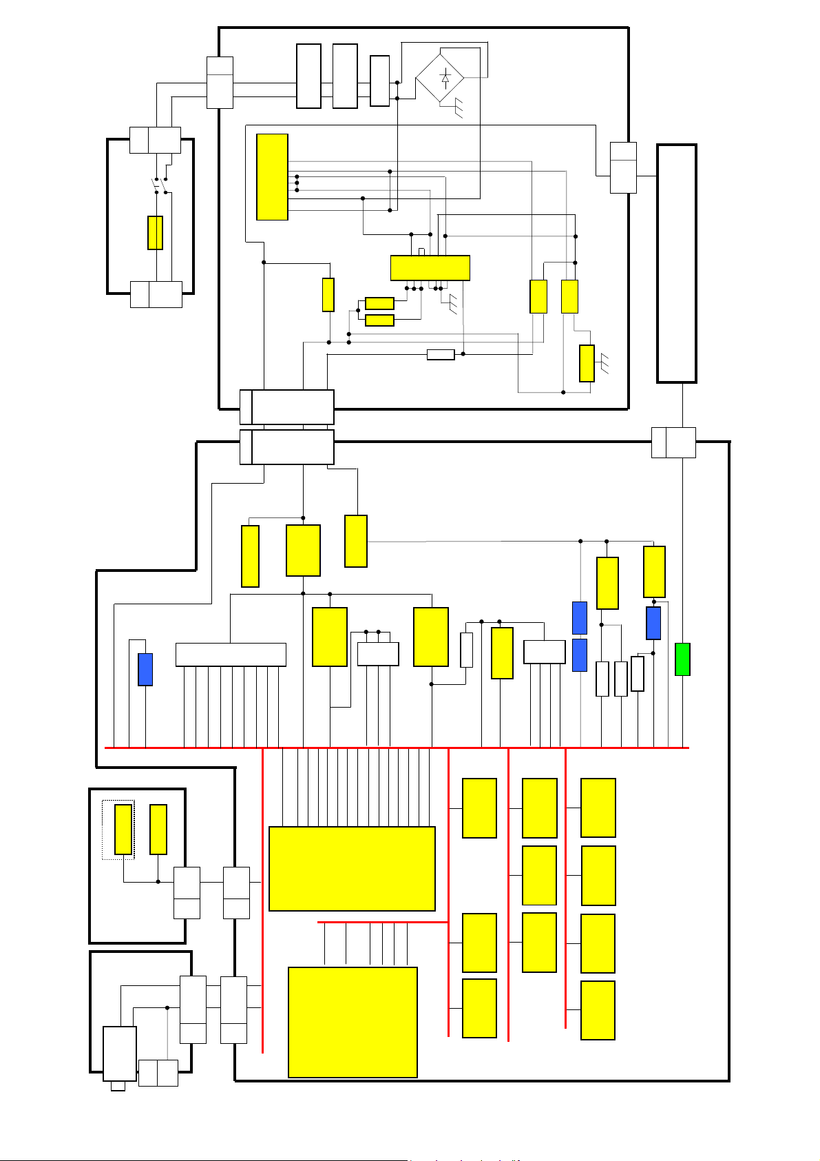
CHASSIS BOARD LAYOUT....................................... 7
LOCATION OF LEAD WIRING................................... 7
SETTING INSPECTION.............................................. 8
SELF-CHECK............................................................. 9
ADJUSTMENT METHOD ......................................... 10
WIRING DIAGRAM……………………………………..11
BLOCK DIAGRAMS.................................................. 12
PARTS LOCATION................................................... 15
REPLACEMENT PARTS LIST.................................. 17
SCHEMATIC DIAGRAMS......................................... 29
A-BOARD (1 OF 5) SCHEMATIC DIAGRAM ...... 30
A-BOARD (2 OF 5) SCHEMATIC DIAGRAM ...... 31
A-BOARD (3 OF 5) SCHEMATIC DIAGRAM ...... 32
A-BOARD (4 OF 5) SCHEMATIC DIAGRAM ...... 33
A-BOARD (5 OF 5) SCHEMATIC DIAGRAM ...... 34
B-BOARD SCHEMATIC DIAGRAM .................... 35
H-BOARD SCHEMATIC DIAGRAM .................... 36
P-BOARD SCHEMATIC DIAGRAM .................... 37
K-BOARD SCHEMATIC DIAGRAM .................... 38
V-BOARD SCHEMATIC DIAGRAM .................... 39
CONDUCTOR VIEWS .............................................. 40
2
Safety Precautions
General Guide Lines
1. When servicing, observe the original lead dress. If a short circuit is found, replace all parts which have been overheated
or damaged by the short circuit.
2. After servicing, see to it that all the protective devices such as insulation barriers, insulation papers shields are properly
installed.
3. After servicing, make the following touch current checks to prevent the customer from being exposed to shock hazards.
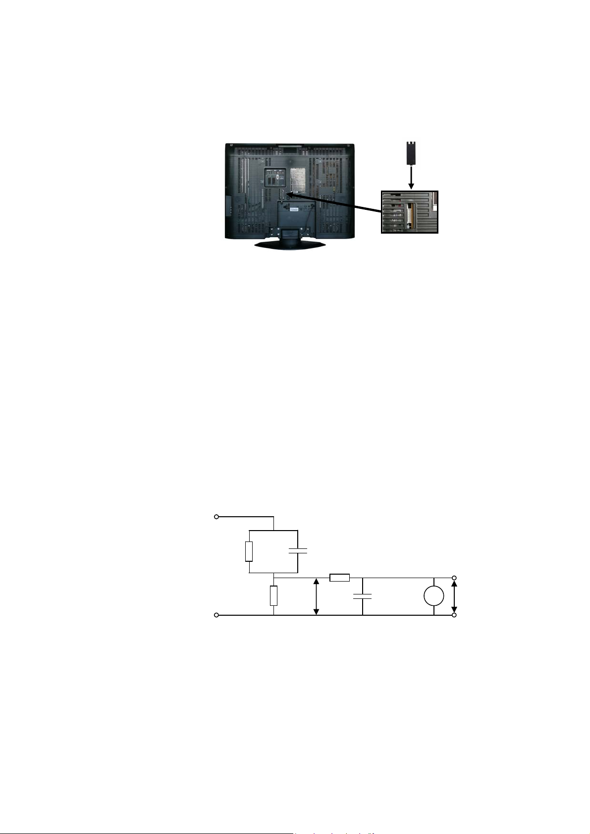
4. Always ensure panel TKP0E16001 is correctly replaced before returning to customer (see Fig.1).
Fig. 1
Touch-Current Check
1. Plug the AC cord directly into the AC outlet. Do not use an isolation transformer for this check.
2. Connect a measuring network for touch currents between each exposed metallic part on the set and a good earth
ground such as a water pipe, as shown in Fig. 2.
3. Use Leakage Current Tester (Simpson 228 or equivalent) to measure the potential acros s the measuring network.
4. Check each exposed metallic part, and measure the voltage at each point.
5. Reserve the AC plug in the AC outlet and repeat each of the above measure.
6. The potential at any point (TOUCH CURRENT) expressed as voltage U1 and U2, does not exceed the following values:
For a. c.: U1 = 35 V (peak) and U2 = 0.35 V (peak);
For d. c.: U1 = 1.0 V,
Note:
The limit value of U2 = 0.35 V (peak) for a. c. and U1 = 1.0 V for d. c. correspond to the values 0.7 mA (peak) a. c. and
2.0 mA d. c.
The limit value U1 = 35 V (peak) for a. c. correspond to the value 70 mA (peak) a. c. for frequencies greater than 100
kHz.
7. In case a measurement is out of the limits specified, there is a possibility of a shock hazard, and the equipment should
be repaired and rechecked before it is returned to the customer.
Measuring network for TOUCH CURRENTS
COLD
WATER PIPE
(EARTH GROUND)
C
=1500:
R
S
TO
APPLIANCES
EXPOSED
METAL PARTS
Resistance values in ohms (:)
V: Voltmetr or oscilloscope
(r.m.s. or peak reading)
NOTE – Appropriate measures should be taken to obtain the correct value in case of non-sinusoidal waveforms
Input resistance: t1M:
Input capacitance:d200pF
Frequency range: 15Hz to 1MHz and d.c.respectively
R0=500:
Fig. 2
=0.22PF
S
U
1
10k:
0.022PF
U2 (V)
V
3

Prevention of Electrostatic Discharge (ESD) to Electrostatically
Sensitive (ES) Devices
Some semiconductor (solid state) devices can be damaged easily by static electricity. Such components commonly are
called Electrostatically Sensitive (ES) Devices. Examples of typical ES devices are integrated circuits and some field-effect
transistors and semiconductor "chip" components. The following techniques should be used to help reduce the incidence of
component damage caused by electrostatic discharge (ESD).
1. Immediately before handling any semiconductor component or semiconductor-equipped assembly, drain off any ESD on
your body by touching a known earth ground. Alternatively, obtain and wear a commercially available discharging ESD
wrist strap, which should be removed for potential shock reasons prior to applying power to the unit under test.
2. After removing an electrical assembly equipped with ES devices, place the assembly on a conductive surface such as
aluminum foil, to prevent electrostatic charge build up or exposure of the assembly.
3. Use only a grounded-tip soldering iron to solder or unsolder ES devices.
4. Use only an anti-static solder removal device. Some solder removal devices not classified as "anti-static (ESD
protected)" can generate electrical charge sufficient to damage ES devices.
5. Do not use freon-propelled chemicals. These can generate electrical charges sufficient to damage ES devices.
6. Do not remove a replacement ES device from its protective package until immediately before you ar e ready to install it.
(Most replacement ES devices are packaged with leads electrically shorted together by conductive foam, aluminum foil
or comparable conductive material).
7. Immediately before removing the protective material from the leads of a replacement ES device, touch the protective
material to the chassis or circuit assembly into which the device will be installed.
Caution
Be sure no power is applied to the chassis or circuit, and observe all other safety precautions.
8. Minimize bodily motions when handling unpackaged replacement ES devices. (Otherwise harmless motion such as the
brushing together of your clothes fabric or the lifting of your foot from a carpeted floor can generate static electricity
(ESD) sufficient to damage an ES device).
IMPORTANT SAFETY NOTICE
There are special components used in this equipment which are important for safety.
These parts are marked by in schematic diagrams, exploded views and replacement parts list. It is essential that
these critical parts should be replaced with manufacturer’s specified parts to prevent shock, fire, or other hazards. Do
not modify the original design without permission of manufacturer.
4
About lead free solder (PbF)
Note: Lead is listed as (Pb) in the periodic table of elements.
In the information below, Pb will refer to Lead solder, and PbF will refer to Lead Free Solder.
The Lead Free Solder used in our manufacturing process and discussed below is (Sn+Ag+Cu).
That is Tin (Sn), Silver (Ag) and Copper (Cu) although other types are available.
This model uses Pb Free solder in it’s manufacture due to environmental conservation issues. For service and repair work,
we’d suggest the use of Pb free solder as well, although Pb solder may be used.
PCBs manufactured using lead free solder will have the PbF within a leaf Symbol
stamped on the back of PCB.
Caution
x Pb free solder has a higher melting point than standard solder. Typically the melting point is 50 ~ 70 °F (30~40°C)
higher. Please use a high temperature soldering iron and set it to 700 ± 20 °F (370 ± 10 °C).
x Pb free solder will tend to splash when heated too high (about 1100 °F or 600 °C).
If you must use Pb solder, please completely remove all of the Pb free solder on the pins or solder area before
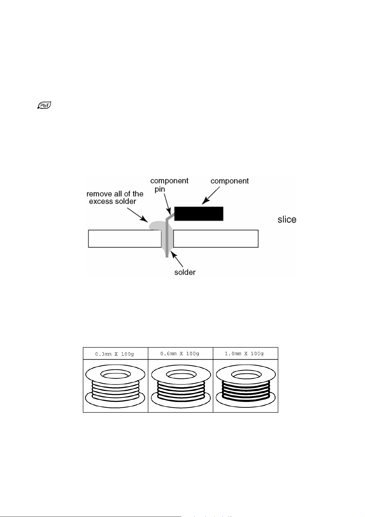
applying Pb solder. If this is not practical, be sure to heat the Pb free solder until it melts, before applying Pb solder.
x After applying PbF solder to double layered boards, please check the component side for excess solder which may
flow onto the opposite side. (see Fig.3)
Fig.3
Suggested Pb free solder
There are several kinds of Pb free solder available for purchase. This product uses Sn+Ag+Cu (tin, silver, copper) solder.
However, Sn+Cu (tin, copper), Sn+Zn+Bi (tin, zinc, bismuth) solder can also be used. (see Fig.4)
Fig.4
5
Service Hints
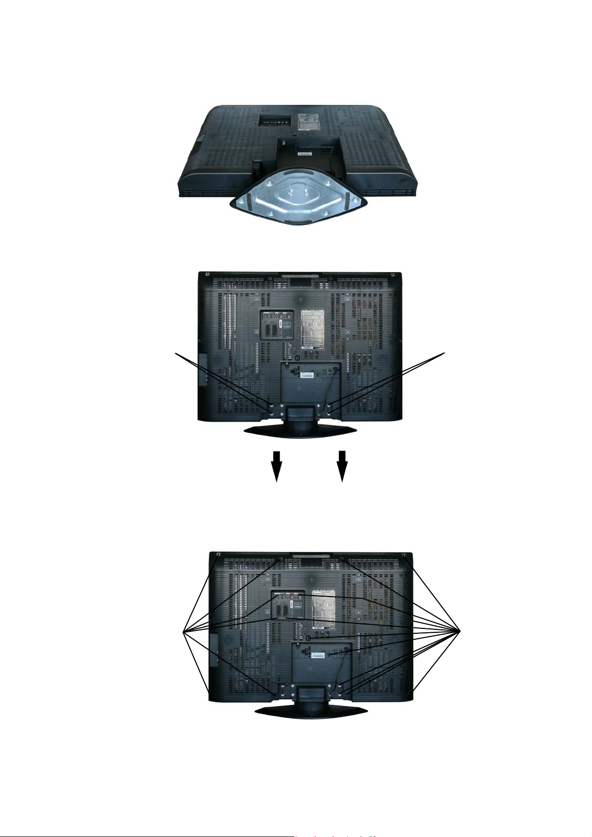
How to remove the Pedestal assembly
Lay the main unit face down. (see Fig.5)
Fig.5
Remove the 4 fixing screws and the pedestal assembly. (see Fig.6)
SCREWS
How to remove the backcover
Remove the 16 [14] fixing screws. (see Fig.7)
SCREWS
SCREWS
Fig.6
SCREWS
6
Fig.7
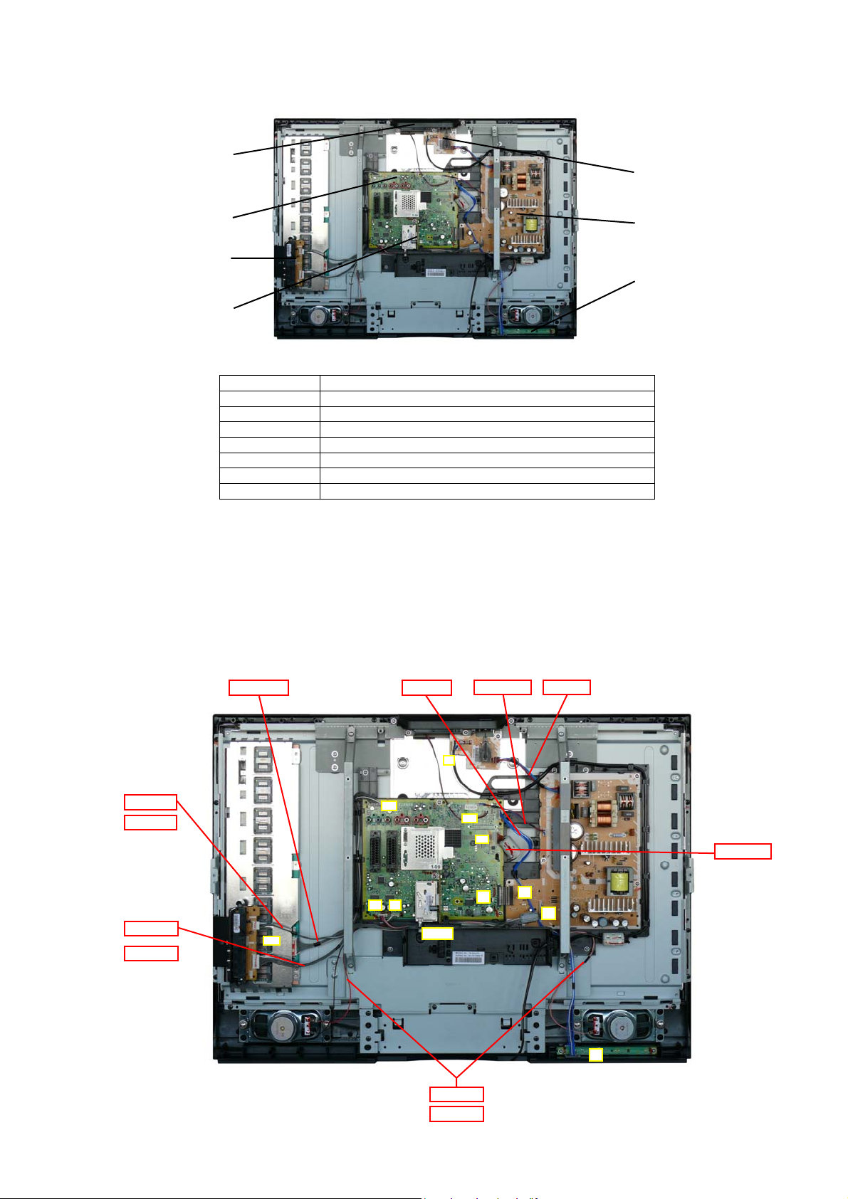
Chassis Board Layout
A5–
A5–
KEY CONTROL
K-BOARD
A-BOARD
H-BOARD
B-BOARD
Board Name Function
A-Board Main Board
B-Board Tuner
H-Board AV3 Terminal
Key Control Key Control
K-Board Mains Input, Power Switch
P-Board Power Supply
V-Board Remote Receiver, LED IR, Bats
Location of Lead Wiring
To find the Part Number of required wire in Replacement Parts List click on the wire name in red box
P-BOARD
V-BOARD
[26´´]
[26´´]
A6 – H2
A6 – H2
A12 – H1
A12 – H1
P3–PAN
CN1
A12
A5 A6
A8–V2
[26´´]
TU001
K1
A13 –P4
A10
A2
A7
SP
SP
K3–P1
A2 –PAN
P2
P3
V2
7

Setting Inspection
Voltage Confirmation
A board Normal mode
Test point Position Voltage Description
TP3800 Connector A7, pin 20
TP3806 Connector A7, pin 8
TP3810 Connector A7, pin 12
TP3811 Q3800, +pin
TP3802
TP3812 D38002, -pin
TP3801 IC3801, pin1
TP3805
TP3815 D3819, -pin
TP3813 C3801, pin
TP3804 C3808, + pin
TP3803 C3818, +pin
P board
TP833 Connector P2, pin 8
TP830 Connector P2, pin 9
TP832 Connector P2, pin 20
TP830 Connector P2, pin 12
TP002 Connector P2, pin 8
TP003 Connector P2, pin 9
Confirm the following voltages:
13,8V r0,7V STBY12V
23,9Vr0,5V SIGNAL24V
23,9V r0,5V AUD24V
3,3V r0,3V 3.3V_HDMI
5,05V r0,25V 5V
8,2r0,5V 8V
9V r0,9V 9V
13,8V r0,7V 12V
30V r2V 30V
Standby mode
5V r0,5V STBY5V
3,3V r0,2V STBY3.3V
1,8r0,1V STBY1.8V
Normal mode
23,9V r0,5V SIGNAL24V
24,2V r0,5V AUD24V
13,8V r0,7V STBY12V
23,9V r0,5V AUD24V
Standby mode
24,2Vr0,5V SIGNAL24V
10V AUD24V
8
Self Check
Self-check is used to automatically check the bus lines and hexadecimal code of the TV set. To enter Self-Check mode, keep
pressing the STATUS button on the remote control and press the down (-/v) button on the TV set. To exit Self Check,
switch off the TV set at the power button.
TX-32LE7FA
TX-32LE7PA
Panasonic 2007LCD
Self Check Complete
E2 O.K.
VCTP O.K.
AVSW O.K.
TUN O.K.
HDMI O.K.
Chassis 21
Model 09
Size 32
VCTP B3
Panasonic 2007LCD
Self Check Complete
E2 O.K.
VCTP O.K.
AVSW O.K.
TUN O.K.
HDMI O.K.
Chassis 21
Model 10
Size 32
VCTP B3
SW V1.12
E2 V02
E2CRC 56
OPTION 1 0F
OPTION 2 00
OPTION 3 B9
OPTION 4 11
OPTION 5 00
OPTION 6 45
OPTION 7 FD
OPTION 8 D8
OPTION 9 00
OPTION 10 00
OPTION 11 13
OPTION 12 20
OPTION 13 1C
CHECK 42
SW V1.12
E2 V02
E2CRC 5F
OPTION 1 0F
OPTION 2 00
OPTION 3 B9
OPTION 4 11
OPTION 5 00
OPTION 6 45
OPTION 7 FD
OPTION 8 58
OPTION 9 00
OPTION 10 00
OPTION 11 13
OPTION 12 20
OPTION 13 1C
CHECK C2
TX-32LE7LA
TX-26LE7PA
Panasonic 2007LCD
Self Check Complete
E2 O.K.
VCTP O.K.
AVSW O.K.
TUN O.K.
HDMI O.K.
Chassis 21
Model 12
Size 32
VCTP B3
Panasonic 2007LCD
Self Check Complete
E2 O.K.
VCTP O.K.
AVSW O.K.
TUN O.K.
HDMI O.K.
Chassis 21
Model 13
Size 26
VCTP B3
SW V1.12
E2 V02
E2CRC CC
OPTION 1 0D
OPTION 2 00
OPTION 3 39
OPTION 4 10
OPTION 5 00
OPTION 6 45
OPTION 7 3C
OPTION 8 58
OPTION 9 00
OPTION 10 40
OPTION 11 13
OPTION 12 28
OPTION 13 0C
CHECK B6
TV V1.12
E2 V02
E2CRC 3E
OPTION 1 0F
OPTION 2 00
OPTION 3 B9
OPTION 4 11
OPTION 5 00
OPTION 6 45
OPTION 7 FD
OPTION 8 58
OPTION 9 00
OPTION 10 00
OPTION 11 13
OPTION 12 40
OPTION 13 1C
CHECK E2
TX-26LE70LA
TX-R32LE7A
Panasonic 2007LCD
Self Check Complete
E2 O.K.
VCTP O.K.
AVSW O.K.
TUN O.K.
HDMI O.K.
Chassis 21
Model 08
Size 26
VCTP B3
Panasonic 2007LCD
Self Check Complete
E2 O.K.
VCTP O.K.
AVSW O.K.
TUN O.K.
HDMI O.K.
Chassis 21
Model 19
Size 32
VCTP B3
TV V1.12
E2 V02
E2CRC AD
OPTION 1 0D
OPTION 2 00
OPTION 3 39
OPTION 4 10
OPTION 5 00
OPTION 6 45
OPTION 7 3C
OPTION 8 58
OPTION 9 00
OPTION 10 40
OPTION 11 13
OPTION 12 48
OPTION 13 0C
CHECK D6
TV V1.12
E2 V02
E2CRC 31
OPTION 1 0F
OPTION 2 00
OPTION 3 B9
OPTION 4 11
OPTION 5 00
OPTION 6 45
OPTION 7 FD
OPTION 8 58
OPTION 9 00
OPTION 10 00
OPTION 11 13
OPTION 12 20
OPTION 13 1C
CHECK C2
TX-26LE7FA
TX-R26LE7A
Panasonic 2007LCD
Self Check Complete
E2 O.K.
VCTP O.K.
AVSW O.K.
TUN O.K.
HDMI O.K.
Chassis 21
Model 14
Size 26
VCTP B3
Panasonic 2007LCD
Self Check Complete
E2 O.K.
VCTP O.K.
AVSW O.K.
TUN O.K.
HDMI O.K.
Chassis 21
Model 20
Size 26
VCTP B3
TV V1.12
E2 V02
E2CRC 3D
OPTION 1 0F
OPTION 2 00
OPTION 3 B9
OPTION 4 11
OPTION 5 00
OPTION 6 45
OPTION 7 FD
OPTION 8 D8
OPTION 9 00
OPTION 10 00
OPTION 11 13
OPTION 12 40
OPTION 13 1C
CHECK 62
TV V1.12
E2 V02
E2CRC 16
OPTION 1 0F
OPTION 2 00
OPTION 3 B9
OPTION 4 11
OPTION 5 00
OPTION 6 45
OPTION 7 FD
OPTION 8 58
OPTION 9 00
OPTION 10 00
OPTION 11 13
OPTION 12 40
OPTION 13 1C
CHECK E2
Display Ref. No. Description P.C.B.
E2 IC1120 EAROM A-Board
VCTP IC1501 AUDIO VIDEO TEXT PROCESSOR A-Board
AVSW IC1501 AV SWITCH A-Board
TUN TU001 TUNER B-Board
HDMI IC1503 HDMI A-Board
If the CCU ports have been checked and found to be incorrect or not located then " - - " will appear in place of "O.K.".
9
Adjustment Method
How to enter Service 1
x Set the Bass to maximum position, set the Treble to minimum position then keep pressing the INDEX button on the
remote control and press the down button (-/v) on the TV set, this will place the TV set into the Service Mode 1.
Key Command
x Press the RED / GREEN buttons to step up / down through the functions.
x Press the YELLOW / BLUE buttons to alter the function values, to alter White Rasters use +/- buttons
x Press the OK button after each adjustment has been made to store the required values.
x To exit the Service Mode, press the "N" button.
Keep adjusting sequence: DVCO, Sub-Contrast, other items.
Item
Sub-Contrast
DVCO
Highlight
Lowlight
Sub-Brightness
White Balance Adjustment
Instrument
x Remote Control
x LCD WB meter (Minolta CA-210 or equivalent)
Condition
x Switch on the TV Set. Enter Service1. Step down to Highlight line and keep the aging time more than 20 minutes.
Procedure
x After aging time above set White Raster No.12 for Highlight and No.4 for Lowlight Press the OK button
to store.
x Put Minolta Sensor to the center of the LCD Panel with 25mm gap between Minolta Sensor and LCD Panel. Adjust "x"
and "y" values by changing Red and Blue values.
x Press OK button to store setting.
Note: All setting values are approximate
High
Low 4 0064 0064 0064
Setting indication
Sub-Contrast
32
DVCO
63
12 0410 0410 0410
Sub-Brightness
0
Settings / Special features
Receive a 80% white level Philips Pattern with correct
sound system (B/G, D/K) via aerial input. For Sub-
Contrast alignment press "Blue" button, wait until the
figure colour is changed from red to black colour.
Press the OK.
Receive a 80% white level Philips Pattern via aerial
input. For DVCO alignment press "Blue" button, wait
until the figure colour is changed from red to black
colour. Press the OK.
For correct setting see White Balance Adjustment
Optimum setting.
High 12
Low 4
Item Value
Highlight
Lowlight
x
y
x
y
2850r150
2940r150
2860r150
2900r150
10
MAINS IN
K1
JK3600
AV3
H-BOARD
TNP0EH009
A6 H2
A12 H1
JK3002
AUDIO
V-BOARD
TNP0EV009
V2
A8
A10
5 KEY BUTTON
SP-R
K-BOARD
TNP0EK009
Wiring diagram
P1 K3
P4
P2
P-BOARD
TNP0EP009
P3
A13
A7
JK3000
AV1
JK3050
AV2
A-BOARD
TNP0EA009
A2
A1
B1
B2
SERVICE
A5 A5
JK5001
HDMI1
JK3001
YUV
JK2300
AUDIO OUT
SP-L
11
LCD-PANEL
B-BOARD
TNP0EA009
JK3001
A
A
A
U
V
L
V
R
L
Y
A5
13
16
423
R
1
13
16
H-BOARD
H1
A12
8
8
AV3 R IN
AV3 L IN
C
Y
R
L
3
1
4
6
4
6
H2
1
3
3
1
1
3
A6
A-BOARD
CVBS OUT
RED/C IN
1520 19
G IN
11
7
B IN
CVBS IN
L IN
R IN
326
L OUT
1
R OUT
AV2 21 PIN SCART
CVBS OUT
Video & Stereo Audio Block Diagram
CVBS IN
R IN
G IN
B IN
L IN
R IN
L OUT
R OUT
19
1 3 2 6 7 11 15 20
AUDIO AMP
IC251
4
SP L
31
IC3300
33
AV1 R OUT32AV1 L OUT
AUDIO AMP
IC252
4
SP R
9
30
AUD_MATRIX
7
AV1 R IN 6AV1 L IN
IC1501
VCT69XYP
91023
8
11
10
V1 AV2 AV3 YUV R IN
V1 AV2 AV3 YUV L IN
1 2 27 28
4
3
YUV R IN
YUV L IN
AV1 R OUT VCTP
AV1 L OUT VCTP
AV1 21 PIN SCART
24
V2 CVBS IN
AV1 R IN
178
190
1
7
IC270
HEDPHONE AMP
3
5
HP L
66-73
B 8Bit data Bus
SPEAKER R
HP R
26
25
27
21
22
MONITOR OUT R
MONITOR OUT L
AV2 B IN
AV2 G IN
AV2 RED/C IN
AV2 CVBS OUT
PR IN
PB IN
179
180
177
176
AV1 G IN
AV1 B IN
172
181
194
174
191
189
195
CVBS IN
AV1 CVBS IN
AV1 CVBS OUT
DATA TO PANEL
Y IN
SIF
31
173
AV3 CVBS IN
184
187
188
SPEAKER L
28
13,14
AM
50-57
58-65
R 8Bit data Bus
G 8Bit data Bus
IC5003
HDMI RECEIVER
8Bit data
AV3 C IN
AV3 Y IN
131110
R
JK3002
L
A1
B1
TUNER CVBS
131110
SIF
AM
A2
TO LCD PANEL
L
JK5001
HDMI
R
JK2300
B-BOARD
TUNER
TU001
ENGF7701GF
12
K3
PC1060
RM1050
,
,
,
,
,
,
,
VSU
C 3,3
,
,
,
,
,
,
,
,
,
,
_
P1
1
3
1
3
LINE
FILTER LF 800
L800
142
LINE
FILTER LF 802
~
3
~
D801
-
P3
K-BOARD
SW 800
F 800
1
K1
4
MAIN IN
P-BOARD
UD24 V
P2
A7
PROTECTION
IC800
7 9 5 3 2 4 1
MAIN PS CONTROL
Q830
SIG24 V
STBY 12 V
12
11
9
9,11,12
SIGNAL 24V
10
8
20-22
10
8
20-22
IC3800
12V STBY
Q3802
D831
D832
12V
T800
12347
141516
13
12
F830
1-5
8
9
10
11
A2
LCD PANEL
26-30
PANEL 5V
PC801
PC800
IC 830
IC3803
IC3802
STBY 3.3V
3V
VSUPAU 8V
VSUPSIF 5V
SUPDIG 3
183336
IC1501
AUDIO VIDEO
PROCESSOR
IC3801
STBY 1.8V
3V
VSUPIO1 3,3V
VSUPDRI 3
77
114
45,75
96
86
124
LCF´S
D5000
3V
SUPDRI 3,3V
AUD24 V
5V
5V MIXED P0
SUPCOM 3,3V
VSUPDIG 3,3V
VSUPIO1 3,3V
VSUPIO3 3
Power Supply Block Diagram
BATS
6
STBY3.3V
V2
3V
3V
SUPVO 3
VSUPFE 3
6
A8
3V
3V
SUPDAC 3
VSUPLVDS 3
HDMI
3.3V
115
V-BOARD
1V8 HD
3V3 HD
B-BOARD
TUNER
TU001
B2
5V
12
4
B1
1
12
4
A1
IC5003
HDMI RECEIVER
5,6,7,13,16,19,26,76,89,109
134
122
22,23,35,74,79,92,94,105,
114,128,139
LCF´S
SUPDIG 1.8V
SUPLVDS 1.8V
SUPFE 1.8V
V
8V
PDA
VSUPFE 1,8V
VSUPLVDS 3,3V
VSUPLVDS 1
142
164
127,133,139,150,156
3V3 PVCC
3V3 XTAL
3V3 AVCC
98
37,55
38,42,46,50,57,61,65,69
Q3803
3.3V HDMI
3V
SUPVO 3,3V
SUPIO3 3
VSUPFE 3,3V
197
192
185
170
169
3V3 REG
99
5V
5V MIXED P0
8V
LCF
3V3 HD
14,9,8,7
8
8
IC5000
1V8 HD
DAC
IC1380
IC5001
EDID EPROM
OP AMP
IC1381
LCF´S
3V3 AVCC
3V3 PVCC
8V
8
IC270
AUDIO 24V
18,5
IC252
UDIO 24V
18,5
IC251
D3807
D3806
LCF
5V
30V 12V
3V3 REG
3V3 XTAL
STBY 3,3VSTBY 3,3VSTBY 3,3V 9V
1,6
HP AMP
AUDIO AMP
AUDIO AMP
IC1220
8
2
IC1500
5
IC3300
SWITCH
EPROM
IC1120
RESET
AUD MATRIX
TUNER 5V
LCF
VSUPAU 8V
LCF
8V
D3802
Q1701
9V
5V PANEL 5V
A-BOARD
13
 Loading...