

Panasonic TC-19LX50, TX-23LX50, TX-19LE50, TX-23LE50 Schematic
Specifications
A
A
A
Y
A
Y
V
A
A
PowerSource
PowerConsumption
LCD 1280 × 768 pixels widescreen LCD panel (TC-19LX50, TC-19LE50)
Screen Size 16.3 “ × 9.8 “ ×18.9 “ (413 mm × 248 mm × 481 mm) (TC-19LX50, TC-19LE50)
(W × H × diagonal) 20.0 “ × 11.3 “ ×23.0 “ (508 mm × 286 mm × 583 mm) (TC-23LX50, TC-23LE50)
Channel Capability VHF-12 : UHF-56 : Cable-125
Sound
Speakers Ø5 cm × 2 pcs, 8 W (TC-19LX50, TC-19LE50)
Audio Output 8 W [4 W + 4 W] (10%THD)
Headphones M3 (3.5 mm) Jack × 1
FEATURES 3D Y/C Digital Comb Filter, CLOSED CAPTION, V-Chip
Operating Conditions Temperature : 41 °F - 95 °F (5 °C - 35 °C)
Connection Terminals
INPUT VIDEO (RCA PIN Type ×1) ×2 1.0 Vp-p (75 W)
COMPONENT
IDEO INPUT (including synchronization)
OUTPUT
LCD Television
TC-19LX50
TC-23LX50
TC-19LE50
TC-23LE50
LH44 Chassis
C 120 V, 60 Hz
verage use : 66 W (TC-19LX50, TC-19LE50)
verage use : 83 W (TC-23LX50, TC-23LE50)
Stand-bycondition : 0.11 W
Power off : 0.1 W
1366 × 768 pixels widescreen LCD panel (TC-23LX50, TC-23LE50)
Ø6 cm × 2 pcs, 8 W (TC-23LX50, TC-23LE50)
Humidity: 5 % - 90 % RH (non-condensing)
S-VIDEO (MINI DIN 4pin ×1) ×2
UDIO L-R (RCA PIN Type ×2) ×2 0.5 Vrms
×1 1.0 Vp-p
PB/PR×1 ±0.35 Vp-p
UDIO L-R (RCA PIN Type ×2) ×1 0.5 Vrms
UDIO L-R (RCA PIN Type ×2) ×1 0.5 Vrms
: 1.0 Vp-p (75 W ),
C : 0.286 Vp-p (75 W)
ORDER NO. ITD0503010CE
B05 Canada:B07
© 2005 Matsushita Electric Industrial Co., Ltd. All
rights reserved. Unauthorized copying and
distribution is a violation of law.
TC-19LX50 / TC-23LX50 / TC-19LE50 / TC-23LE50
Dimensions ( W × H × D )
Including TV Stand 20.2 “ × 18.1 “ × 10.2 “ (514 mm × 459 mm × 259 mm) (TC-19LX50, TC-19LE50)
24.1 “ × 19.9 “ ×10.2 “ (612 mm × 505 mm × 259 mm) (TC-23LX50, TC-23LE50)
TV Set Only 20.2 “ × 15.6 “ ×4.9 “ (514 mm × 395 mm × 125 mm) (TC-19LX50, TC-19LE50)
24.1 “× 17.4 “ ×4.9 “ (612 mm × 441 mm × 125 mm) (TC-23LX50, TC-23LE50)
Mass (Weight) 8.5 kg (18.7 lb.) NET (TC-19LX50, TC-19LE50)
9.5 kg (20.9 lb.) NET (TC-23LX50, TC-23LE50)
Note:
Design and Specifications are subject to change without notice. Weight and Dimensions shown are approximate.
CONTENTS
Page Page
1 Safety Precautions 3
1.1. General Guidelines
2 Warning
2.1. Prevention of Electro Static Discharge (ESD) to
Electrostatically Sensitive (ES) Devices
2.2. About lead free solder (PbF)
3 Location of Controls and Components
4 Service Mode
4.1. How to enter into adjustment mode
4.2. Cancellation
4.3. Contents of adjustment mode
5 Troubleshooting Guide
5.1. Self-check function
6 Disassembly and Assembly Instructions
6.1. Removing the hinge cover
6.2. Removing the pedestal
6.3. Removing the back cover (TC-23LX50/LE50)
6.4. Removing the back cover (TC-19LX50/LE50)
6.5. Removing the tuner cover
6.6. Removing the shield cover
6.7. Removing the button panel and K-board
6.8. Removing the chassis
6.9. Removing the A-Board, AP-Board and Power Unit
6.10. Removing the speaker, and V-Board
6.11. Removing the LCD mount metal
6.12. Removing the LCD panel (TC-23LX50/LE50)
6.13. Removing the LCD panel (TC-19LX50/LE50)
6.14. Removing the LCD fixing metal
6.15. Location of Lead Wiring
7 Measurements and Adjustments
3
3
3
4
5
6
6
6
6
7
7
8
8
8
8
8
8
9
9
9
9
10
10
10
11
11
12
7.1. Video Signal Level Adjustment (RF)
8 Block Diagram
8.1. Block Diagram (1 of 3)
8.2. Block Diagram (2 of 3)
8.3. Block Diagram (3 of 3)
9 Wiring Connection Diagram
10 Schematic Diagrams
10.1. Schematic Diagram Notes
10.2. A-Board (1 of 6) Schematic Diagram
10.3. A-Board (2 of 6) Schematic Diagram
10.4. A-Board (3 of 6) Schematic Diagram
10.5. A-Board (4 of 6) Schematic Diagram
10.6. A-Board (5 of 6) Schematic Diagram
10.7. A-Board (6 of 6) Schematic Diagram
10.8. AP-Board Schematic Diagram
10.9. K-Board and V-Board Schematic Diagram
11 Printed Circuit Views
11.1. A-Board
11.2. AP-Board
11.3. K-Board and V-Board
12 Exploded View and Replacement Parts List
12.1. Parts Layout
12.2. Packing Exploded Views
12.3. Mechanical Replacement Parts List
13 Electrical Parts List
13.1. Electrical Parts List Notes
13.2. Electrical Replacement Parts List
13
13
15
15
16
17
19
21
21
22
23
24
25
26
27
28
29
31
31
34
35
37
37
38
39
40
40
41
2
TC-19LX50 / TC-23LX50 / TC-19LE50 / TC-23LE50
Caution
Be sure no power is applied to the chassis or circuit, and observe all other safety precautions.
8. Minimize bodily motions when handling unpackaged replacement ES devices. (Otherwise hamless motion such as the brushing
together of your clothes fabric or the lifting of your foot from a carpeted floor can generate static electricity (ESD) sufficient to
damage an ES device).
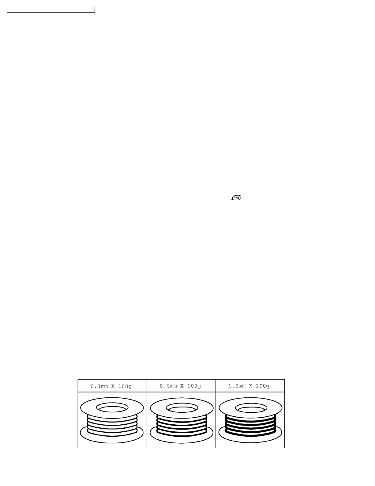
2.2. About lead free solder (PbF)
Note: Lead is listed as (Pb) in the periodic table of elements.
In the information below, Pb will refer to Lead solder, and PbF will refer to Lead Free Solder.
The Lead Free Solder used in our manufacturing process and discussed below is (Sn+Ag+Cu).
That is Tin (Sn), Silver (Ag) and Copper (Cu) although other types are available.
This model uses Pb Free solder in it’s manufacture due to environmental conservation issues. For service and repair work, we’d
suggest the use of Pb free solder as well, although Pb solder may be used.
PCBs manufactured using lead free solder will have the PbF within a leaf Symbol
Caution
· Pb free solder has a higher melting point than standard solder. Typically the melting point is 50 ~ 70 °F (30~40°C) higher.
Please use a high temperature soldering iron and set it to 700 ± 20 °F (370 ± 10 °C).
· Pb free solder will tend to splash when heated too high (about 1100 °F or 600 °C).
If you must use Pb solder, please completely remove all of the Pb free solder on the pins or solder area before applying Pb
solder. If this is not practical, be sure to heat the Pb free solder until it melts, before applying Pb solder.
· After applying PbF solder to double layered boards, please check the component side for excess solder which may flow onto
the opposite side. (see figure below)
Suggested Pb free solder
There are several kinds of Pb free solder available for purchase. This product uses Sn+Ag+Cu (tin, silver, copper) solder.
However, Sn+Cu (tin, copper), Sn+Zn+Bi (tin, zinc, bismuth) solder can also be used.
stamped on the back of PCB.
4
http://getMANUAL.com
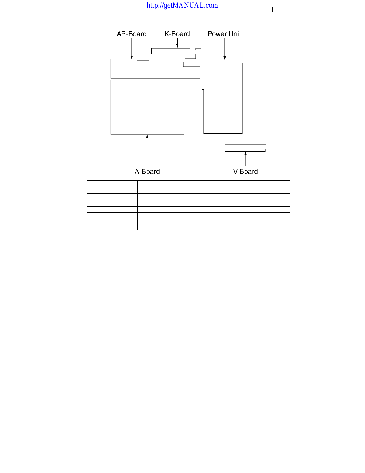
3 Location of Controls and Components
TC-19LX50 / TC-23LX50 / TC-19LE50 / TC-23LE50
Board Name Function
A-Board Main (AV Switch, Audio, MCU, Grobal Core, AV connector )
V-Board Remote Reciever
K-Board Power switch, Control swtich
AP-Board DC-DC
Power Unit Power (AC/DC),
None serviceable.
Power Unit should be exchange for service.
5
TC-19LX50 / TC-23LX50 / TC-19LE50 / TC-23LE50
4 Service Mode
4.1. How to enter into adjustment mode
While pressing [VOLUME- ] button of the main unit, press [RECALL] button of the remote control three times in a row (within 2
seconds).
4.1.1. Adjustment method.....Use the remote control.
“1” button...Main items Selection in forward direction
“2” button...Main items Selection in reverse direction
“3” button...Sub items Selection in forward direction
“4” button...Sub items Selection in reverse direction
“VOL” button...Value of sub items change in forward direction (
), in reverse direction ( )
4.2. Cancellation
Switch off the power with the [POWER] button on the main unit or the [POWER] button on the remote control.
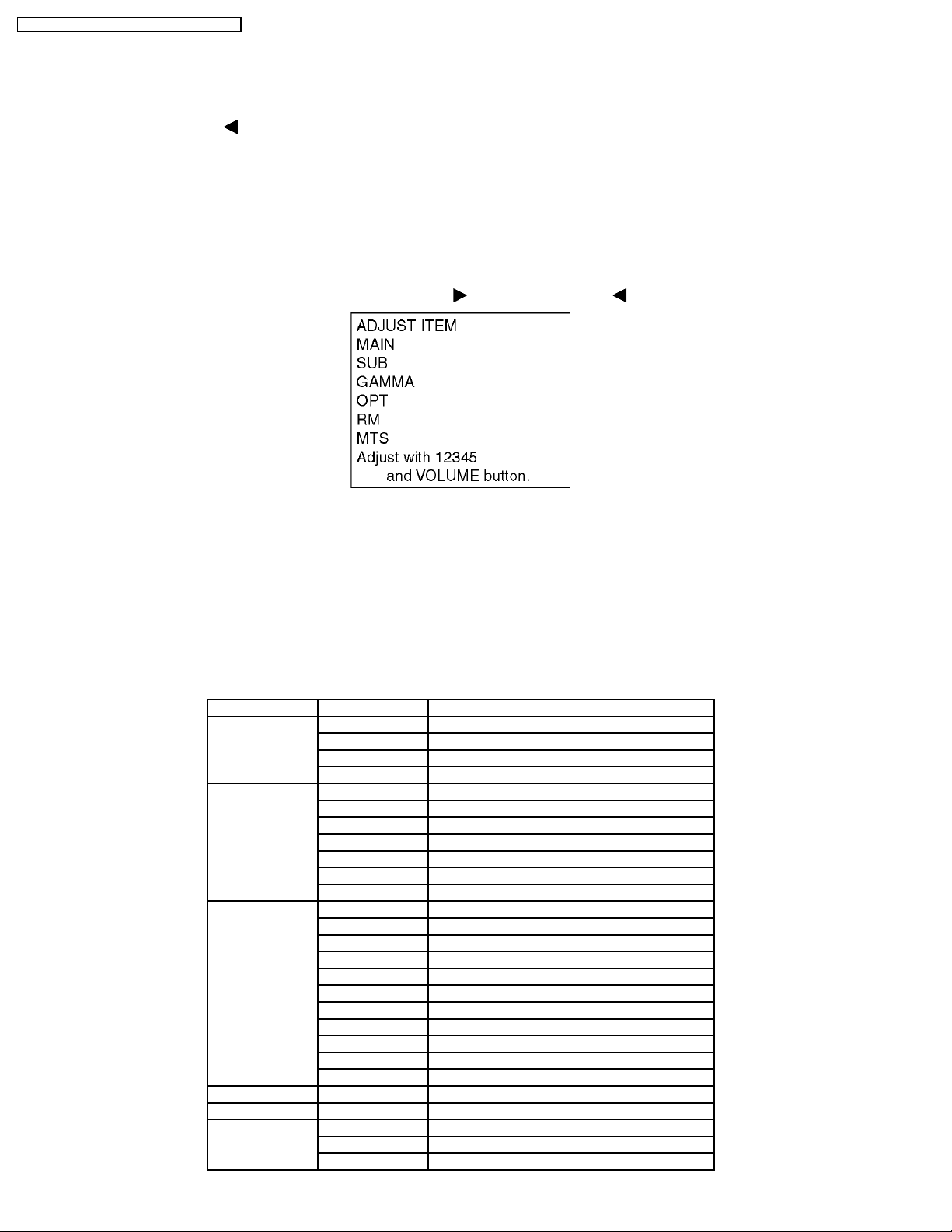
4.3. Contents of adjustment mode
· Value is shown as a hexadecimal number.
· Preset value differs depending on models.
· After entering the adjustment mode, take note of the value in each item before starting adjustment.
Main item Sub item Remarks
MAIN YGAIN Video Level (RF, VIDEO, S, COMPONENT)
B-Y Video Level (RF, VIDEO, S, COMPONENT)
R-Y Video Level (RF, VIDEO, S, COMPONENT)
PILEN PILEN Current
SUB COLOR Sub color
TINT Sub tint
BACK-L Sub back light
BRIGHT Sub bright
B-Y-G B-Y Gain
R-Y-A R-Y demodulation axis
TEMP Temp data
GAMMA WHITE Test pattern (100% White)
RED Test pattern (100% Red)
GREEN Test pattern (100% Green)
BLUE Test pattern (100% Blue)
GRAY Test pattern (50% White)
R-GAIN Test pattern (100% White) R-GAIN
G-GAIN Test pattern (100% White) G-GAIN
B-GAIN Test pattern (100% White) B-GAIN
R-CENT Test pattern (50% White ) R-CENT
G-CENT Test pattern (50% White) G-CENT
B-CENT Test pattern (50% White) B-CENT
OPT OPT00 (TV)
RM CODE Remote control code A or B
MTS MTSIN RF Audio input
SEPAH Stereo separation Hi
SEPAL Stereo separation Low
6
TC-19LX50 / TC-23LX50 / TC-19LE50 / TC-23LE50
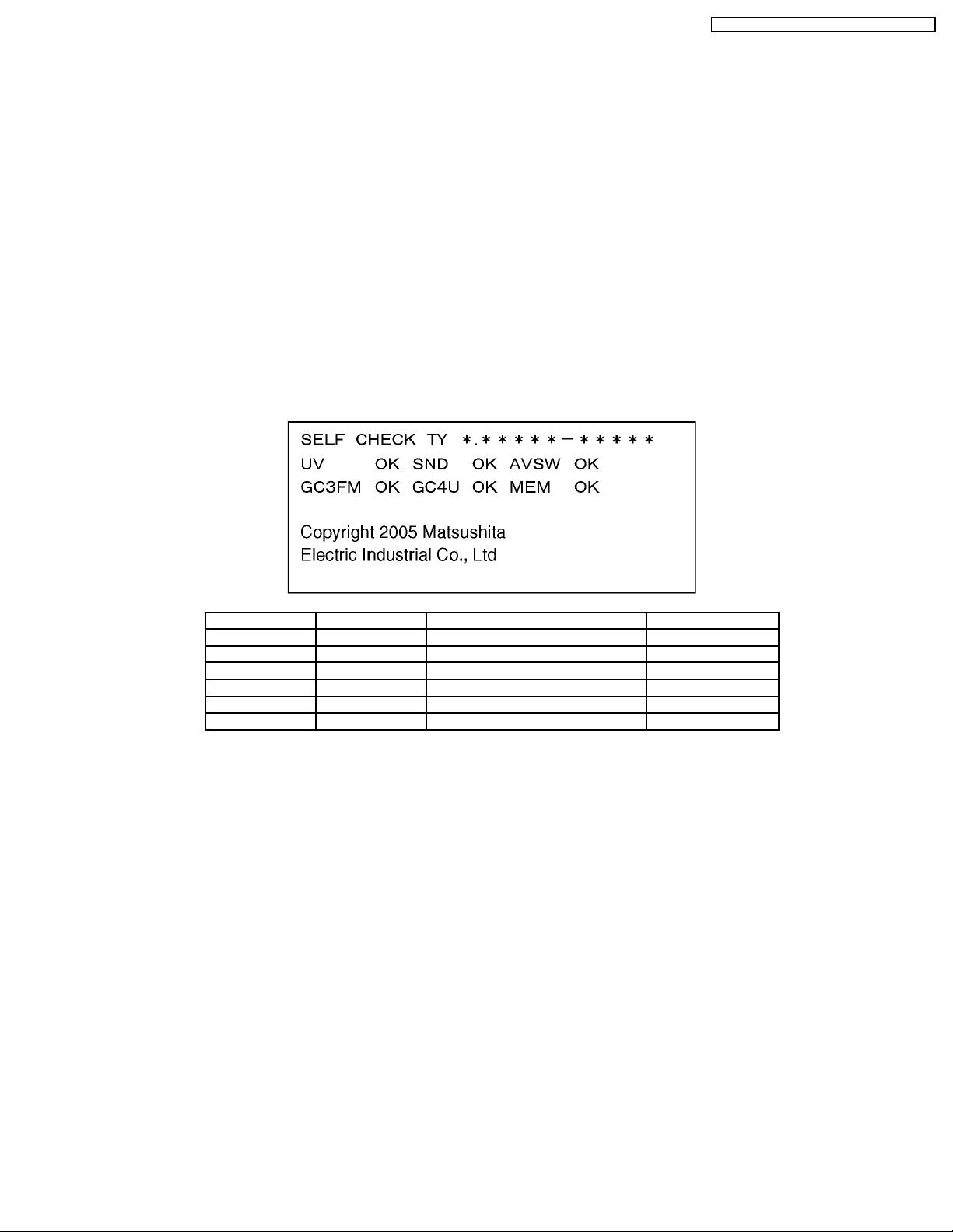
5 Troubleshooting Guide
5.1. Self-check function
When phenomena like "the power fails from time to time" or "the video/audio fails from time to time" can not be confirmed at the
time of servicing, the self-check function can be used to confirm the occurrence and to limit the scope for the defective circuits.Also,
when "the power fails from time to time", display on the screen can be used to confirm the occurrence and to limit the scope for
the defective circuits.
Any programmed channels, channels caption data and some other user defined settings will be erased and return to factory setting.
5.1.1. How to access
5.1.1.1. Access
Produce TV reception screen and, while pressing [VOLUME-] button on the main unit, press [SLEEP] button on the remote
controller unit simultaneously.
5.1.1.2. Exit
When one of the buttons for channel selection etc. is pressed, the display returns to the normal screen.
5.1.2. Screen display
Display Ref No. Description P.C.B
UV TU001A Tuner A-Board
SND IC2301 Sound Control A-Board
AVSW IC3007 AV Switch A-Board
GC3FM IC4023 Global Core Main A-Board
GC4U IC4016 Global Core A-Board
MEM IC1104 EEPROM A-Board
7

TC-19LX50 / TC-23LX50 / TC-19LE50 / TC-23LE50
6 Disassembly and Assembly Instructions
6.1. Removing the hinge cover
1. Lay down the unit so that the rear cover faces upward.
2. Remove the screw.
3. Remove the hinge cover.
6.2. Removing the pedestal
1. Remove the 4 screws.
2. Remove the pedestal.
6.4. Removing the back cover (TC19LX50/LE50)
1. Remove the 14 screws.
2. Remove the back cover.
6.5. Removing the tuner cover
6.3. Removing the back cover (TC23LX50/LE50)
1. Remove the 15 screws.
2. Remove the 2 screws.
3. Remove the back cover.
1. Remove the 2 screws.
2. Remove the tuner cover.
8

6.6. Removing the shield cover
TC-19LX50 / TC-23LX50 / TC-19LE50 / TC-23LE50
6.8. Removing the chassis
1. Remove the 5 screws.
2. Remove the shield cover.
6.7. Removing the button panel
and K-board
1. Remove the 2 screws.
2. Remove the 2 screws.
3. Remove the button panel.
1. Remove the 5 screws.
2. Disconnect the coupler (A2, A5, AP5 and AP6).
3. Remove the chassis.
6.9. Removing the A-Board, APBoard and Power Unit
1. Remove the 10 screws.
2. Disconnect the coupler (A3-AP3, A4-AP4 and AP1-CN1).
3. Remove A-Board, AP-Board and Power Unit.
4. Disconnect the coupler (K5).
5. Remove the K-Board.
9

TC-19LX50 / TC-23LX50 / TC-19LE50 / TC-23LE50
6.10. Removing the speaker, and VBoard
6.11. Removing the LCD mount
metal
1. Remove the 8 screws.
2. Remove the speaker.
3. Remove the 2screw.
4. Disconnect the coupler (V1 and V2).
5. Remove the V-Board.
1. Remove the 5 screws.
2. Remove the LCD mount metal (bottom).
3. Remove the screw.
4. Remove the LCD mount metal (top).
6.12. Removing the LCD panel (TC23LX50/LE50)
1. Remove the 2 screws.
2. Remove the LCD panel.
10

6.13. Removing the LCD panel (TC19LX50/LE50)
1. Remove the 14 screws.
2. Remove the LCD panel.
6.14. Removing the LCD fixing
metal
TC-19LX50 / TC-23LX50 / TC-19LE50 / TC-23LE50
1. Remove the 4 screws.
2. Remove the LCD fixing metal (L/R)
11

TC-19LX50 / TC-23LX50 / TC-19LE50 / TC-23LE50
6.15. Location of Lead Wiring
12

TC-19LX50 / TC-23LX50 / TC-19LE50 / TC-23LE50
7 Measurements and Adjustments
7.1. Video Signal Level Adjustment (RF)
Instrument Name Connect to Remarks
1. Remote controller
2. RF signal
3. SG
1. Receive studio color bar by RF signal input.
(Viewing mode: standard, LCD AI: OFF, Back Light: +30 )
2. In service mode choose adjust item then press remote button 1 into main mode then press remote 3 into Y Gain and press
remote button “8” to do auto adjustment.
3. Press remote button “2” go back main menu.
RF in
13

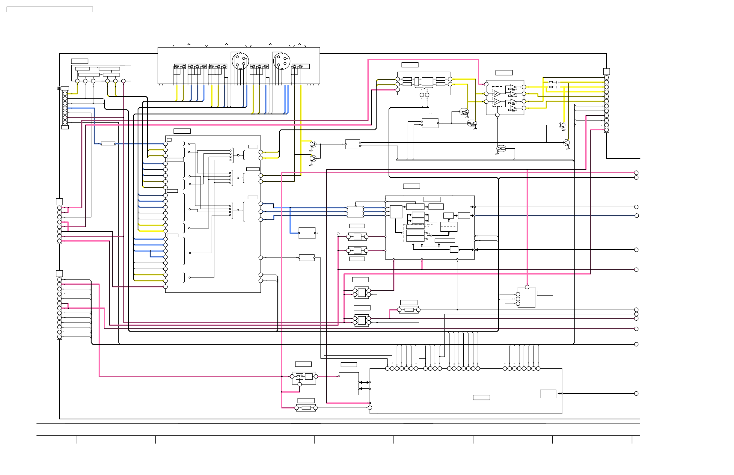
8 Block Diagram
8.1. Block Diagram (1 of 3)
http://getMANUAL.com
TC-19LX50 / TC-23LX50 / TC-19LE50 / TC-23LE50
K-BOARD
SW3805
R3818
R3821
SW3804
VOLVOL
K5
2
KEYSCAN
3
RELAY
4
STB+5V
5
MAIN_SW_DET
6
+5VS
R3816
SW3808
R3817
SW3806
CH
PUSH
R3815
SW3803
A
TV/VTR
SW3807
CH
POWER SWITCH
AP-BOARD
AP6
2
3
4
MAIN_SW_DET
5
6
MAIN+9V
Q861
Q862
2
2
7.5V(PANEL_5V OVP)
DC-DC ON/OFF
D869
D873
11V(SUB_9V OVP)
D872
D876
D882
D884
D890
D889
R913
L:NORMAL
H:ABNORMAL
Q865
+30V(BT)/+5V(P)
SHORT DET
Q864
SOS DET
IC851
SUB+9V
1
AVR
KEY
IC854
PANEL+5V
AVR
1
5
Q856
PANEL 5V ON/OFF
Q857
R910
B
D879
R891
R896
R900
Q859
R892
D887
POWER UNIT
RC1
R3
0.1
D14
D11
D13
D12
RECTIFIER
1
2
SWITCHING REG
+
C6
330u
R9
DRIVE
CONTROL
Z2
4
3
D7
D6
22K
4
OSC
5
3
D10
D8
DD1
STBY 5V
GENE
COLD
C
D
AC CORD
2
1
CN1
HOT
COLD
SWITCHING TRANS
D17
6
5
HOT
T2
7
6
D24
4
D5
1
2
D18
C12
47u
RL1
5V
+
C21
1000u
HOT
C13
2200p
15
13
12
D9
COLD
RC3
RC2
PC2
FEED BACK
POWER ON/OFF
+32V
+
C23
220u
+24V
+++
+
C17
100u
R14
1K
R14
150
Q2
C19
C18
100u
100u
+32V
RELAY
+5VS
AP1
19
1
2
3
4
14
13
11
CN2
1
19
+24V(INV)
18
D23
D21
R19
1K
R18
2.2K
+24V(INV)
17
+24V(INV)
16
+24V(INV)
6
7
9
POWER_ON
IC855
Q869
R932
R930
R931
Q868
D886
SOUND+10V
AVR
1
5
Q854
DC-DC ON/OFF
IC853
SUB+5V
1
2
AVR
R933
2
BT_30V
R935
Q870
R934
13V(SOUND_10V OVP)
MAIN+3.3V
1
D871
R936
R937
D877
D878
IC852
AVR
5
Q855
DC-DC ON/OFF
D875
7.5V(SUB_5V OVP)
2
DC-DC ON/OFF CONTROL
Q866
TO
LCD PANEL
(INVERTER)
Q867
AP3
4
5
9
13
15
18
20
22
AP4
1
3
MAIN_SW_DET
KEY
INV_SOS
INV_ADIM
INV_PWM
INV_ON
INV_ON
INV_PWM
INV_SOS
INV_ADIM
1417131812
11
4
1
2
+24V(INV)
+24V(INV)
+24V(INV)
5143
+24V(INV)
+24V(INV)
INV_SOS
INV_ON
INV_ADIM
INV_PWM
AP4
6
7
8
10
11
13
14
15
16
E
TC-19/23LX50, TC-19/23LE50
Block Diagram (1/3)
TC-19/23LX50, TC-19/23LE50 Block Diagram (1/3)
2
746
81 53
15
TC-19LX50 / TC-23LX50 / TC-19LE50 / TC-23LE50
8.2. Block Diagram (2 of 3)
TUNER
UV IN
S_CLOCK
S_ DATA
VIDEO
BT30V
5V(S)
SOUND_10V
SOUND_10V
BT_30V
SUB_9V
MAIN_9V
SUB9V
SUB_5V
MAIN_3.3V
TV_SOS
STB_5V
MAIN_ON
MAIN_SWDET
SUB_ON
PANEL_5V
PANEL_5V
KEY
INV_SOS
PANEL_ON
INV_ADIM
INV_PWM
INV_ON
TU001
SIF
AFT
A-BOARD
14
10
11
17
15
3
12
A3
4
5
9
13
15
18
20
22
A4
1
3
6
7
8
10
11
13
14
15
16
17
18
IC2202
SIF
SCL
SDA
VIDEO
BTL
+B
AFT
FILTER
14
TV_SOS
MAIN_ON
MAIN_SW
SUB_ON
INV_SOS
PANEL_ON
INV_ADIM
INV_PWM
INV_ON
MTS DEMODULATER
IIC
19 22
18
SCL1
SDA1
KEY
DEMODU
21
Q001
BUFFER
MATRIX
L
TV-L
COMPONENT
PR
PB
D1_PR
PRGLRG
AV SW
D1_PB
Y
PB
D1_Y
L
R
+5V(M)
R
7
TV-R
NCNCNC
D1_R
D1_L
IC3001
TV
U/V-V
24
TV-L
TV-R
D1-Y
D1-PB
D1-PR
D1-L
D1-R
V1-Y
V1-V
V1-C
V1_DET
V1-S
V1-L
V1-R
V2-Y
V2-V
V2-C
V2_DET
V2-S
V2-L
V2-R
AFT
V
21
L
22
R
COMPONENT
26
Y
28
PB
30
PR
27
L
29
R
VIDEO1
8
Y
V
2
6
C
33
V1 DET
S DET
7
4
L
5
R
VIDEO2
14
Y
10
V
12
C
44
S2 DET
19
V2 DET
13
S DET
9
L
11
R
57
+9V(S)
VIDEO1
AV1
C
V
L
R
Y
V1_L
V1_R
V1_V
V1_DET
V1_S
Y
C-GGV-SWVLRG
V1_C
V1_Y
MONITOR
S CLOCK
S DATA
AUDIO
L-OUT
R-OUT
L-OUT
R-OUT
VIDEO
VIDEO2
V
L
R
V2_V
V2_S
V2_L
V2_DET
V2_R
MAIN-L
49
MAIN-R
51
39
40
54
V/Y
C/Pb
56
Pr
64
52
SY
SCL1
59
SDA1
61
MONITOR
AV2
C
R
Y
C-GGV-SWVLRGCYGY-G
V2_C
V2_Y
IR
OUT
MONITOR
L
NCNCLRGCYGY-G
NC
Q3002
AUDIO DEF
JK3001A
NC
Q3003
AUDIO DET
Q3001
AUDIO
DEFFET
CONTROL
MAIN-L
MAIN-R
IC2301
SOUND CONTROL
L AMP
1
R AMP
2
26
+9V(M)
MAIN_SW
MON_DEF
BASS
TREBLE
VOL
BLANCE
30 31
SDA1
SCL1
Q2303 Q2306,
Q2312,Q2314
MUTE
CIRCUIT
MUTE
L OUT
R OUT
25
24
Q2311
MUTE(R)
Q2310
MUTE(L)
1
6
8
Q1107
INV
IC2302
AUDIO OUT
+11V(SOUND)
AMP
9
ADJ
C2323
16V
100u
R2329
R2333
C2326
16V
Q2308
HP MUTE(L)
Q2307
HP MUTE(R)
+
+
100u
G_LED
R_LED
RM
AI
L(+)
2
L(-)
4
R(+)
12
R(-)
10
VOL
A2
2
SP(R+)
7
HP(R+)
6
HP(L+)
5
SP(L+)
3
SP(L-)
4
SP(R-)
10
LED G
11
LED R
12
STB+3.3V
13
REMOTE
15
16
+5V(S)
AI
1
2
IC4023
DIGITAL CORE, 3D Y/C SEP
IC4032
Q4045-Q4047
Q4022-Q4024
IC1103
STB+3V
1
5
IC1102
2
CVBS
FILTER
SELECT
H:fc 30MHz
L:fc 14MHz
CC
CIRCUIT
RESET
Q4006-Q4014
MAIN3.3V
CLAMP
CIRCUIT
IC4021
AD+2.5V
5
5
IC4020
PLL+2.5V
AVR
AVR
IC4029
MAIN+2.5V
1
AVR
8
V/Y
C/Pb
Pr
4
4
2
5
(10bit)
2.5V(AD)
2.5V(PLL)
+2.5V(M)
A/D
IC4024
IC4030
MAIN+1.8V
1
2
AVR
8
5
IC1105
FLASH MEMORY
AVR
2
4
+3.3V(STB)
DATA
ADR
125
DATA_I/O
ADDRESS
STB+3.3V
RESET
78
RESET
51
INV_ON
INV_SOS
MAIN_SW
110
105
115
89
CC
INV ON
MAIN SW DET
CVBS FLTR ON/OFF
CLAMP
ID1/ED2
MOVE DET
2D
Y/C SEP
3D
Y/C SEP
KEY
97
KEYSCAN
INV SOS
SELF
WIDE
DET
+3.3V(M)
SUB_ON
22
AC ON
GC3FM
SYNC SEP
DET
TV_SOS
MAIN_ON
111
21
MAIN ON
LINE MEMORY
AFT
96
15
AFT
TV SOS
CHROMA
LUMINANCE
PANEL_ON
PANEL5V_ON
SKEW
DEMODU
PROCESS
SCL0A
56
S CLOCK0A
I/F
55
RESET
SDA0A
S D ATA0A
DIGITAL
I/F
S_CLOCK2
SCL0B
24
S CLOCK0B
S_DATA2
SDA0B
23
S D ATA0B
CLK
HS/VS
YUV
(10bit)
SCL2
SDA2
8
109
EEPROM WP
VOL
MON_DEF
92
VOL
6
5
7
MUTE
MON DEF
STB_3.3V
SCL
SDA
WP
AI
66
91
A MUTE
RM
102
REMOTE
AI SENSOR
R_LED
26
27
LED R
IC1104
EEPROM
G_LED
LED G
OSD OUT
(16bit)
OSD DATA
16bit
HV/CLK
SCL0A
SDA0A
SRQ
SCL1
SDA1
117
116
60
SRQ
S DATA1
S CLOCK1
114
IC1103
3
4
5
6
7
8
9
10
11
12
MCU
TC-19/23LX50, TC-19/23LE50 Block Diagram (2/3)
8
11 159 1410 12
16
TC-19/23LX50, TC-19/23LE50 Block Diagram (2/3)
13
 Loading...