

Page 1
y
A
A
ORDER NO. ITD0509054CE
High Definition Plasma Display
TH-65PHD8BK
TH-65PHD8EK
TH-65PHD8UK
GPH8D Chassis
D10
Specifications
Power Source (UK) 120 VAC, 50/60Hz
Power Source (BK/EK) 220 - 240 VAC, 50/60 Hz
Power Consumption (UK)
Maximum 675 W
Stand-bycondition Save OFF 0.7 W, Save ON 0.5 W
Power off condition 0.2 W
Power Consumption (BK/EK)
Normal use 615 W
Stand-bycondition Save off 0.9 W, Save on 0.7 W
Power off condition 0.35 W
Plasma Displaypanel Drive method:AC type 65-inch, 16:9 aspect ratio
Contrast Ratio 3000:1
Screen size 56.5” (1,434 mm) (W) × 31.7” (806 mm) (H) × 65” (1,645 mm) (diagonal)
(No. of pixels) 1,049,088 (1,366 (W) × 768 (H)) [4,098 × 768 dots]
Operating condition
Temperature 32 °F - 104 °F (0 °C - 40 °C)
Humidit
Applicablesignals
Color System NTSC, PAL, PAL60, SECAM, Modified NTSC
Scanning format 525 (480) / 60i 60p, 625 (575)/50i 50p, 750 (720)/60p 50p, 1125 (1080) / 60i 50i 24p 25p
PC signals VGA, SVGA, XGA, SXGA, UXGA..... (compressed)
Connection terminals
V VIDEO IN / OUT (BNC) 1.0 Vp-p (75-ohm or high impedance)
20 % - 80 %
30p 24sF .... SMPTE274M, 1250 (1080) / 50i
Horizontal scanning frequency 15 - 110 kHz
Vertical scanning frequency 48 - 120 Hz
S VIDEO IN (MINI DIN 4PIN) Y: 1 Vp-p (75-ohm), C: 0.286 Vp-p (75-ohm)
UDIO IN (RCA PIN JACK × 2) 0.5 Vrms (high impedance)
© 2005 Matsushita Electric Industrial Co., Ltd. All
rights reserved. Unauthorized copying and
distribution is a violation of law.
Page 2
Y
A
Y
/
/
A
A
y
y
TH-65PHD8BK / TH-65PHD8EK / TH-65PHD8UK
COMPONENT / RGB (UK)
PC (UK) (HIGH-DENSITYMini-D-SUB 15PIN) R,G,B/0.7 Vp-p (75-ohm)
PC (BK/EK) (HIGH-DENSITYMini-D-SUB 15PIN) R,G,B/0.7 Vp-p (75-ohm)
SERIAL EXTERNAL CONTROL TERMINAL (D-SUB 9PIN) RS-232C COMPATIBLE
SPEAKERS (8Ω) 20 W [10 W + 10 W] (10 % THD)
Accessories Supplied
Remote Control Transmitter EUR7636070R
(UK)
Remote Control Transmitter EUR7636090R
(BK/EK)
Batteries (UK) 2×AASize
Batteries (BK/EK) 2 × R6 Size
Fixing bands (TMME203) × 2
Dimensions (W×H×D) 61.2” (1,554 mm) × 36.4” (925 mm) × 3.9” (99 mm)
Mass (weight) (UK)
main unit onl
with speakers approx. 181.7 lbs
Mass (weight) (BK/EK)
main unit onl
with speakers approx. 82.4 kg
/ G (BNC) 1.0 Vp-p/composite (75-ohm)
0.7 Vp-p/non-composite (75-ohm)
PB/B (BNC), PR/R (BNC) 0.7 Vp-p (75-ohm)
UDIO IN (RCA PIN JACK × 2) 0.5 Vrms (high impedance)
HD, VD/1.0 - 5.0 Vp-p (high impedance)
Component
:1.0 Vp-p (75-ohm : include sync)
P
CB:0.7 Vp-p (75-ohm)
B
P
CR:0.7 Vp-p (75-ohm)
R
UDIO IN (M3 JACK) 0.5 Vrms (high impedance)
HD, VD/1.0 - 5.0 Vp-p (high impedance)
UDIO IN (M3 JACK) 0.5 Vrms (high impedance)
(exclusive of protruding portion)
approx. 172.0 lbs
approx. 78.0 kg net
Notes:
· Design and specifications are subject to change without notice. Mass and dimensions shown are approximate.
· This equipment complies with the EMC standards listed below. EN55022, EN55024, EN61000-3-2, EN61000-3-3. (BK/EK)
CONTENTS
Page Page
1 Applicable signals 5
2 Safety Precautions
2.1. General Guidelines
3 Prevention of Electro Static Discharge (ESD) to
Electrostatically Sensitive (ES) Devices
4 About lead free solder (PbF)
5 PCB Structure sheet of GPH8D chassis
6 Service Hint
7 Disassembly
10
11
6
6
7
8
9
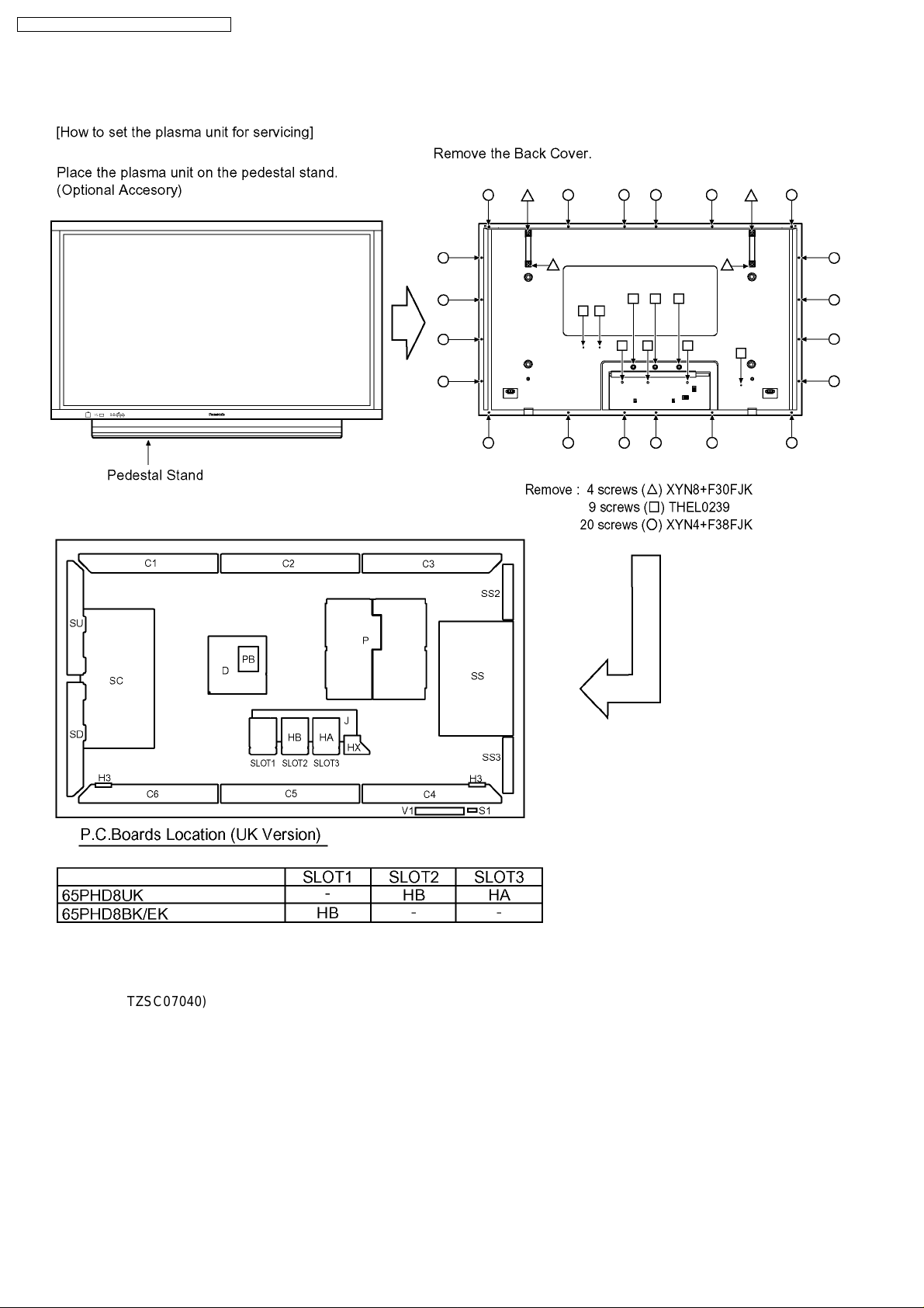
7.1. Removal of the Back Cover
7.2. Removal of the HA-Board and the HB-Board
7.3. Removal of the Slot Block
7.4. Removal of the J-Board
7.5. Removal of the HX-Board
7.6. Removal of the PB-Board
7.7. Removal of the D-Board
7.8. Removal of the P-Board
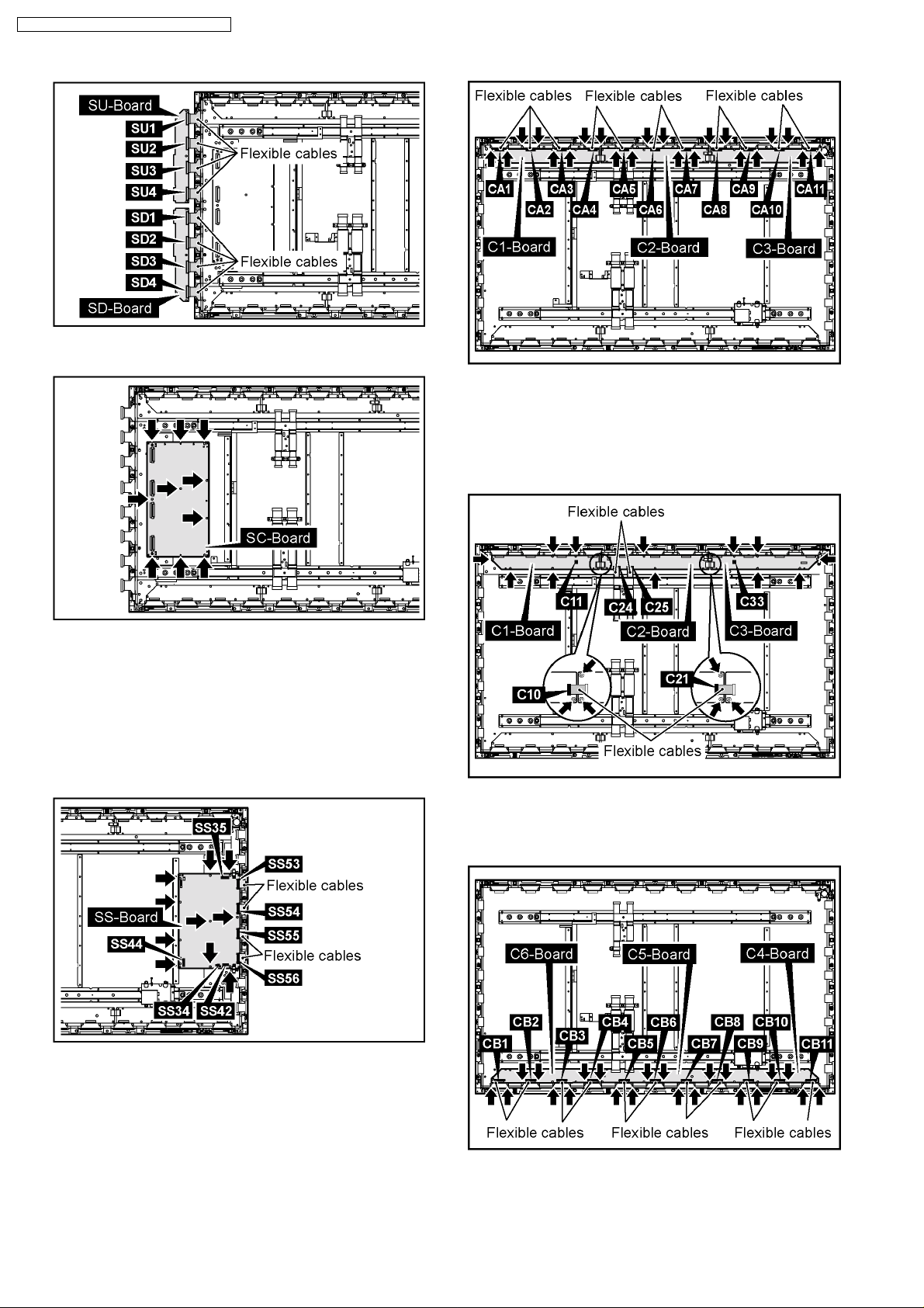
7.9. Removal of the SU-Board and the SD-Board
11
11
12
12
12
12
13
13
15
2
Page 3
TH-65PHD8BK / TH-65PHD8EK / TH-65PHD8UK
7.10. Removal of the SC-Board 15
7.11. Removal of the SS2-Board and the SS3-Board
7.12. Removal of the SS-Board
7.13. Removal of the H3-Board (L, R)
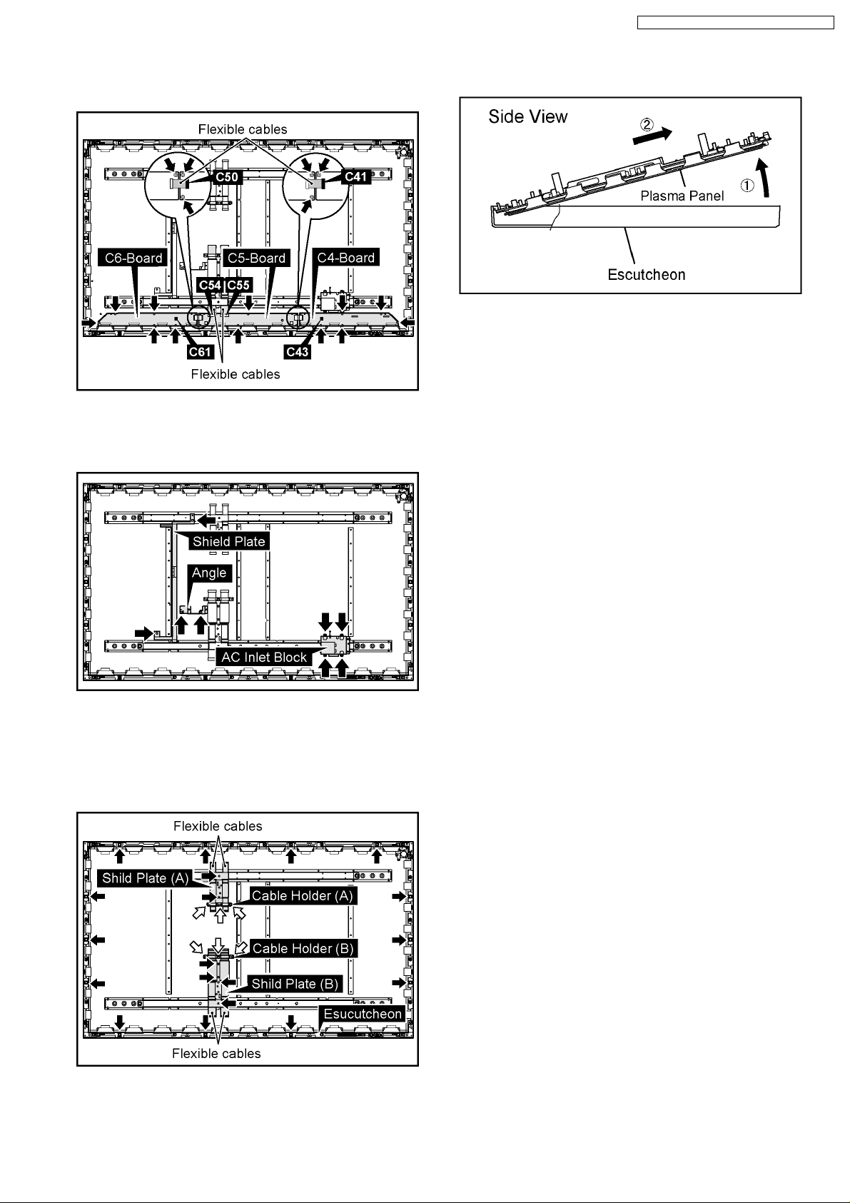
7.14. Removal of the C1, C2, C3, C4, C5 and the C6-Board
7.15. Removal of the Fan
7.16. Removal of the Escutcheon
7.17. Removal of the S1-Board and the V1-Board
7.18. Removal of the Plasma Panel
8 Location of Lead Wiring
9 Adjustment Procedure
9.1. Driver Set-up
9.2. Initialization Pulse Adjust
9.3. P.C.B. (Printed Circuit Board) Remove
9.4. Adjustment Volume Location
9.5. Test Point Location
10 Service mode
10.1. CAT (computer Aided Test) mode
10.2. IIC mode structure (following items value is sample data.)
11 Alignment
11.1. PC / RGB panel white balance
11.2. HD / 525ip / 625ip panel white balance
12 Trouble shooting guide
12.1. Self Check
12.2. No Power
12.3. No Picture
12.4. Local screen failure
13 Option Setting
14 Circuit Board Layout
14.1. P-Board (P-1), (P-2)
14.2. PB-Board
14.3. HA-Board
14.4. HB-Board
14.5. HX-Board
14.6. J-Board
14.7. D-Board
14.8. C1-Board
14.9. C2-Board
14.10. C3-Board
14.11. C4-Board
14.12. C5-Board
14.13. C6-Board
14.14. SC-Board
14.15. SU-Board
14.16. SD-Board
14.17. SS-Board
14.18. SS2 and SS3-Board
14.19. H3, S1 and V1-Board
15 Schematic Diagrams
15.1. Schematic Diagram Notes
15.2. Main Block Diagram
15.3. P-Board (1 of 2)Block Diagram
15.4. P-Board (2 of 2)Block Diagram
16
16
16
17
18
19
20
21
24
26
26
27
27
28
28
29
29
31
32
32
34
36
36
37
37
38
39
41
41
45
46
47
48
49
51
53
54
55
56
57
58
59
62
63
64
67
68
69
69
70
71
72
15.5. P-Board (1 of 3) Schematic Diagram
15.6. P-Board (2 of 3) Schematic Diagram
15.7. P-Board (3 of 3) Schematic Diagram
15.8. PB and V1-Board Block and Schematic Diagram
15.9. HA-Board Block and Schematic Diagram
15.10. HB-Board Block Diagram
15.11. HB-Board (1 of 2) Schematic Diagram
15.12. HB-Board (2 of 2) Schematic Diagram
15.13. HX-Board Block and Schematic Diagram
15.14. J-Board (1 of 2) and H3-Board Block Diagram
15.15. J-Board (2 of 2) Block Diagram
15.16. J-Board (1 of 4) and H3-Board Schematic Diagram
15.17. J-Board (2 of 4) Schematic Diagram
15.18. J-Board (3 of 4) Schematic Diagram
15.19. J-Board (4 of 4) Schematic Diagram
15.20. D-Board (1 of 2) Block Diagram
15.21. D-Board (2 of 2) Block Diagram
15.22. D-Board (1 of 12) Schematic Diagram
15.23. D-Board (2 of 12) Schematic Diagram
15.24. D-Board (3 of 12) Schematic Diagram
15.25. D-Board (4 of 12) Schematic Diagram
15.26. D-Board (5 of 12) Schematic Diagram
15.27. D-Board (6 of 12) Schematic Diagram
15.28. D-Board (7 of 12) Schematic Diagram
15.29. D-Board (8 of 12) Schematic Diagram
15.30. D-Board (9 of 12) Schematic Diagram
15.31. D-Board (10 of 12) Schematic Diagram
15.32. D-Board (11 of 12) Schematic Diagram
15.33. D-Board (12 of 12) Schematic Diagram
15.34. C1, C2, C5 and C6-Board Block Diagram
15.35. C2, C3, C4 and C5-Board Block Diagram
15.36. C1-Board (1 of 2) Schematic Diagram
15.37. C1-Board (2 of 2) Schematic Diagram
15.38. C2-Board (1 of 2) Schematic Diagram
15.39. C2-Board (2 of 2) Schematic Diagram
15.40. C3-Board (1 of 2) Schematic Diagram
15.41. C3-Board (2 of 2) Schematic Diagram
15.42. C4-Board (1 of 2) Schematic Diagram
15.43. C4-Board (2 of 2) Schematic Diagram
15.44. C5-Board (1 of 2) Schematic Diagram
15.45. C5-Board (2 of 2) Schematic Diagram
15.46. C6-Board (1 of 2) Schematic Diagram
15.47. C6-Board (2 of 2) Schematic Diagram
15.48. SC, SU and SD-Board Block Diagram
15.49. SC-Board (1 of 3) Schematic Diagram
15.50. SC-Board (2 of 3) Schematic Diagram
15.51. SC-Board (3 of 3) Schematic Diagram
15.52. SU-Board (1 of 2) Schematic Diagram
15.53. SU-Board (2 of 2) Schematic Diagram
15.54. SD-Board (1 of 2) Schematic Diagram
15.55. SD-Board (2 of 2) Schematic Diagram
15.56. SS, S1, SS2 and SS3-Board Block Diagram
15.57. SS-Board (1 of 2), S1, SS2 and SS3-Board Schematic
Diagram
73
74
75
76
77
78
79
80
81
82
83
84
85
86
87
88
89
90
91
92
93
94
95
96
97
98
99
100
101
102
103
104
105
106
107
108
109
110
111
112
113
114
115
116
117
118
119
120
121
122
123
124
125
3
Page 4

TH-65PHD8BK / TH-65PHD8EK / TH-65PHD8UK
15.58. SS-Board (2 of 2) Schematic Diagram 126
16 Parts Location
16.1. Exploded View
16.2. Cable relation
16.3. Packing summary
127
127
129
130
17 Mechanica l Replacement Parts List
18 Replacement Parts List
18.1. Relpacement Parts List Notes
18.2. Electrical Replacement Parts List
133
134
134
135
4
Page 5
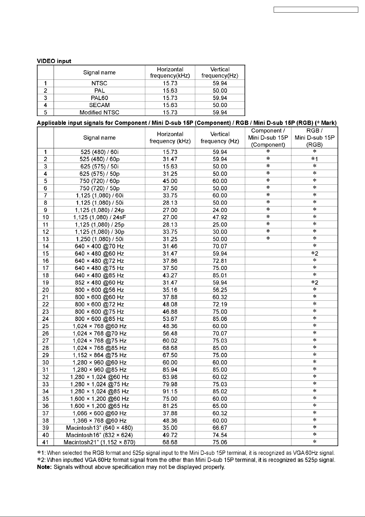
1 Applicable signals
TH-65PHD8BK / TH-65PHD8EK / TH-65PHD8UK
5
Page 6
TH-65PHD8BK / TH-65PHD8EK / TH-65PHD8UK
2 Safety Precautions
2.1. General Guidelines
1. When servicing, observe the original lead dress. If a short circuit is found, replace all parts which have been overheated or
damaged by the short circuit.
2. After servicing, see to it that all the protective devices such as insulation barriers, insulation papers shields are properly
installed.
3. After servicing, make the following leakage current checks to prevent the customer from being exposed to shock hazards.
2.1.1. Leakage Current Cold Check
1. Unplug the AC cord and connect a jumper between the two
prongs on the plug.
2. Measure the resistance value, with an ohmmeter, between
the jumpered AC plug and each exposed metallic cabinet
part on the equipment such as screwheads, connectors,
control shafts, etc. When the exposed metallic part has a
return path to the chassis, the reading should be between
1MΩ and 5.2MΩ.
When the exposed metal does not have a return path to
the chassis, the reading must be
.
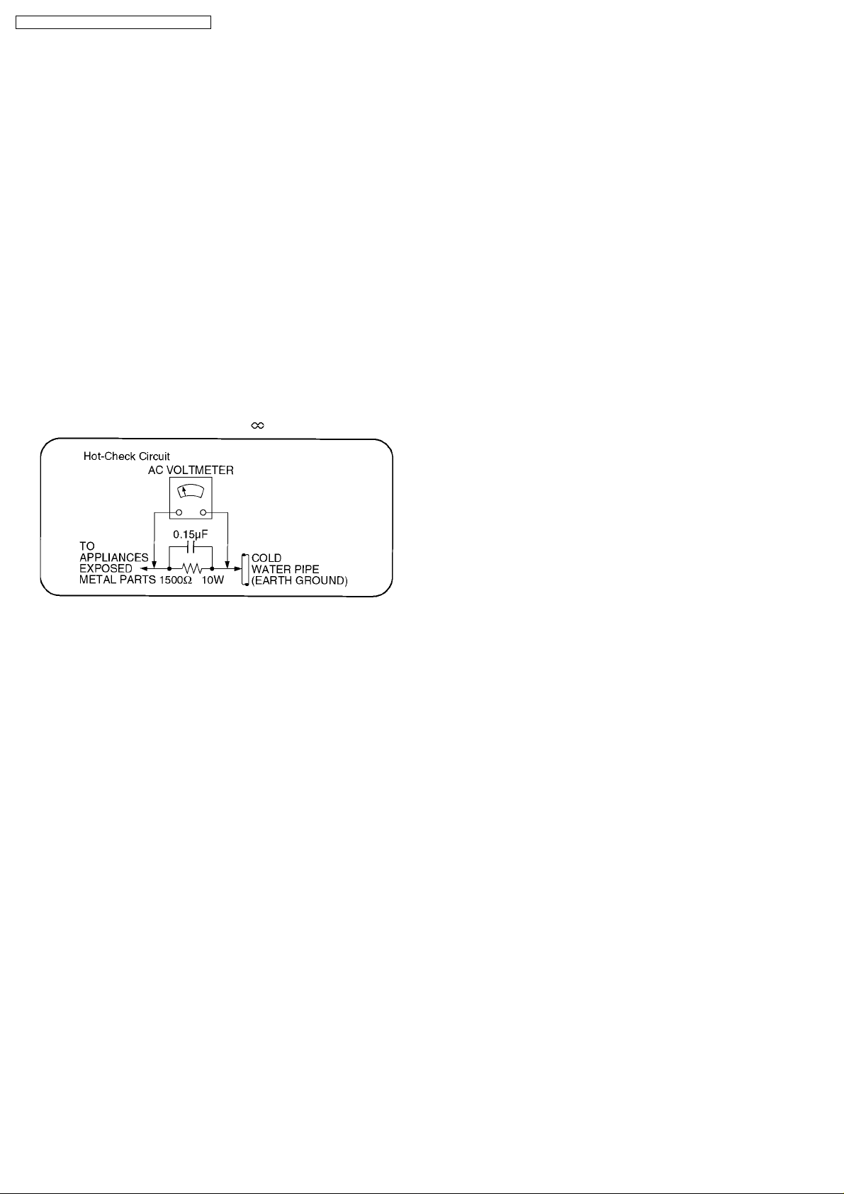
Figure 1
2.1.2. Leakage Current Hot Check (See
Figure 1 .)
1. Plug the AC cord directly into the AC outlet. Do not use an
isolation transformer for this check.
2. Connect a 1.5kΩ, 10 watts resistor, in parallel with a 0.15µF
capacitors, between each exposed metallic part on the set
and a good earth ground such as a water pipe, as shown in
Figure 1 .
3. Use an AC voltmeter, with 1000 ohms/volt or more
sensitivity, to measure the potential across the resistor.
4. Check each exposed metallic part, and measure the
voltage at each point.
5. Reverse the AC plug in the AC outlet and repeat each of the
above measurements.
6. The potential at any point should not exceed 0.75 volts
RMS. A leakage current tester (Simpson Model 229 or
equivalent) may be used to make the hot checks, leakage
current must not exceed 1/2 milliamp. In case a
measurement is outside of the limits specified, there is a
possibility of a shock hazard, and the equipment should be
repaired and rechecked before it is returned to the
customer.
6
Page 7
TH-65PHD8BK / TH-65PHD8EK / TH-65PHD8UK
3 Prevention of Electro Static Discharge (ESD) to
Electrostatically Sensitive (ES) Devices
Some semiconductor (solid state) devices can be damaged easily by static electricity. Such components commonly are called
Electrostatically Sensitive (ES) Devices. Examples of typical ES devices are integrated circuits and some field-effect transistors and
semiconductor "chip" components. The following techniques should be used to help reduce the incidence of component damage
caused by electro static discharge (ESD).
1. Immediately before handling any semiconductor component or semiconductor-equipped assembly, drain off any ESD on your
body by touching a known earth ground. Alternatively, obtain and wear a commercially available discharging ESD wrist strap,
which should be removed for potential shock reasons prior to applying power to the unit under test.
2. After removing an electrical assembly equipped with ES devices, place the assembly on a conductive surface such as
aluminum foil, to prevent electrostatic charge buildup or exposure of the assembly.
3. Use only a grounded-tip soldering iron to solder or unsolder ES devices.
4. Use only an anti-static solder Remove device. Some solder Remove devices not classified as "anti-static (ESD protected)" can
generate electrical charge sufficient to damage ES devices.
5. Do not use freon-propelled chemicals. These can generate electrical charges sufficient to damage ES devices.
6. Do not remove a replacement ES device from its protective package until immediately before you are ready to install it. (Most
replacement ES devices are packaged with leads electrically shorted together by conductive foam, aluminum foil or comparable
conductive material).
7. Immediately before removing the protective material from the leads of a replacement ES device, touch the protective material
to the chassis or circuit assembly into which the device will be installed.
Caution
Be sure no power is applied to the chassis or circuit, and observe all other safety precautions.
8. Minimize bodily motions when handling unpackaged replacement ES devices. (Otherwise hamless motion such as the brushing
together of your clothes fabric or the lifting of your foot from a carpeted floor can generate static electricity (ESD) sufficient
todamage an ES device).
7
Page 8
TH-65PHD8BK / TH-65PHD8EK / TH-65PHD8UK
4 About lead free solder (PbF)
Note: Lead is listed as (Pb) in the periodic table of elements.
In the information below, Pb will refer to Lead solder, and PbF will refer to Lead Free Solder.
The Lead Free Solder used in our manufacturing process and discussed below is (Sn+Ag+Cu).
That is Tin (Sn), Silver (Ag) and Copper (Cu) although other types are available.
This model uses Pb Free solder in it’s manufacture due to environmental conservation issues. For service and repair work, we’d
suggest the use of Pb free solder as well, although Pb solder may be used.
PCBs manufactured using lead free solder will have the PbF within a leaf Symbol
Caution
· Pb free solder has a higher melting point than standard solder. Typically the melting point is 50 ~ 70 °F (30~40 °C) higher.
Please use a high temperature soldering iron and set it to 700 ± 20 °F (370 ± 10 °C).
· Pb free solder will tend to splash when heated too high (about 1100 °F or 600 °C).
If you must use Pb solder, please completely remove all of the Pb free solder on the pins or solder area before applying Pb
solder. If this is not practical, be sure to heat the Pb free solder until it melts, before applying Pb solder.
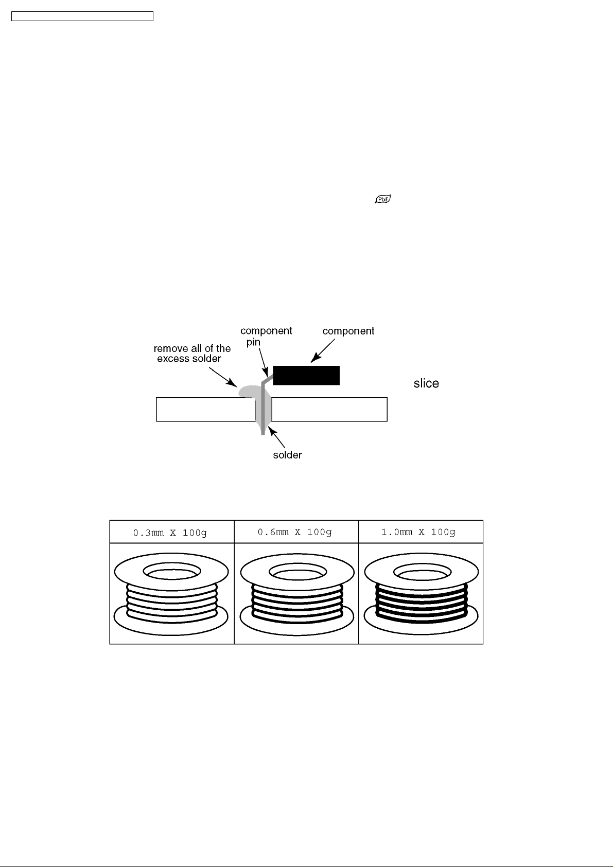
· After applying PbF solder to double layered boards, please check the component side for excess solder which may flow onto
the opposite side. (see figure below)
Suggested Pb free solder
There are several kinds of Pb free solder available for purchase. This product uses Sn+Ag+Cu (tin, silver, copper) solder.
However, Sn+Cu (tin, copper), Sn+Zn+Bi (tin, zinc, bismuth) solder can also be used.
stamped on the back of PCB.
8
Page 9
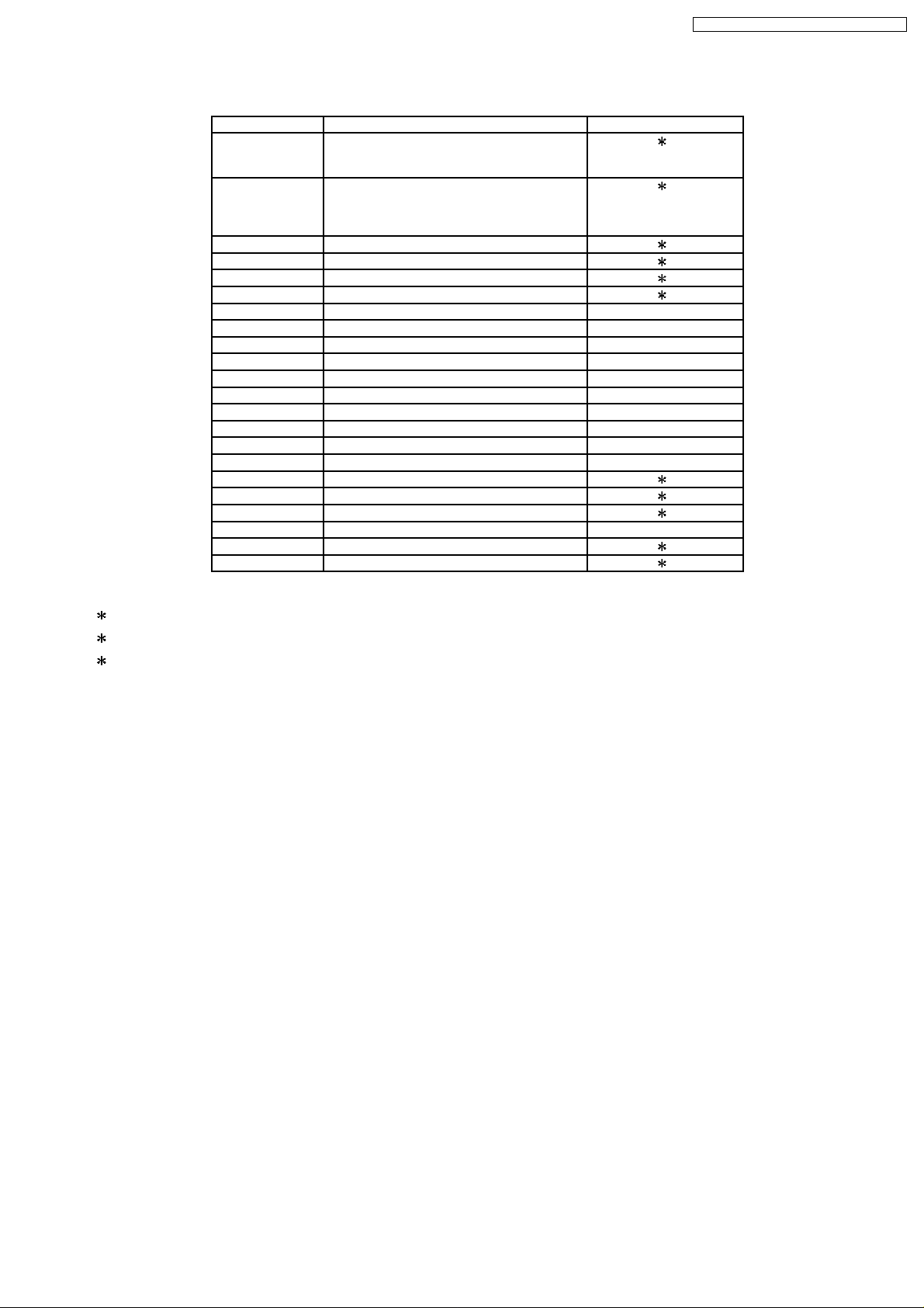
5 PCB Structure sheet of GPH8D chassis
Board Name Function Remarks
D Digital Signal Processor,
Format Converter,
Plasma AI Processor
J Slot Interface (Audio/Video/Sync input Switch),
SYNC processor, Audio processor,
Speaker out amplifier,
DC-DC converter
SS Sustain drive 1
SC Scan drive 1
SU Scan out (Upper) 1
SD Scan out (Lower) 1
C1 Data Drive (Upper Right)
C2 Data Drive (Upper Center)
C3 Data Drive (Upper Left)
C4 Data Drive (Lower Left)
C5 Data Drive (Lower Center)
C6 Data Drive (Lower Right)
H3 Speaker terminal
S1 Power switch
SS2 Sustain out (Upper)
SS3 Sustain out (Lower)
V1 LED (stand-by / Power on) & Remote receiver 1
PB Fan control 1
P Line filter, Power supply 1
HX PC / RS-232C
HB BNC Composite Video 2
HA BNC Component Video 3
TH-65PHD8BK / TH-65PHD8EK / TH-65PHD8UK
1
1
Remarks
1: Recommend PCB´s for initial service for GPH8D chassis.
2: For TH-65PHD8BK/EK/UK
3: For TH-65PHD8UK
9
Page 10
TH-65PHD8BK / TH-65PHD8EK / TH-65PHD8UK
6 Service Hint
Note:
Extension cable kit for Slot Board is supplied as service fixtures and tools.
(Part No. TZSC07040)
10
Page 11
TH-65PHD8BK / TH-65PHD8EK / TH-65PHD8UK
7 Disassembly
· To remove P.C.B., wait for 1 minute after power was off for
discharge from electrolysis capacitors.
and marks indicate screw positions.
·
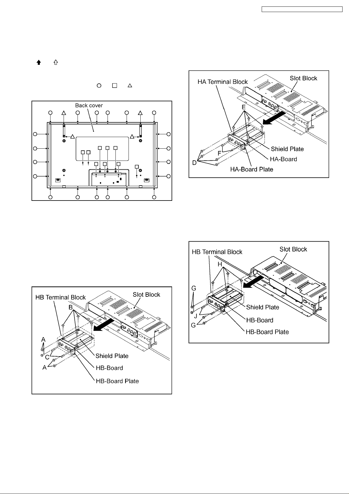
7.1. Removal of the Back Cover
1. Remove the screws (×20 ,×9 ,×4 ) and then remove
the Back Cover.
7.2. Removal of the HA-Board and
the HB-Board
7.2.1. TH-65PHD8UK
· Removal of the HA-Board
1. Remove the 4 screws (D) of the HA Terminal Block and
then remove the HA Terminal Block.
2. Remove the 4 screws (E).
3. Remove the 2 screws (F) and then remove the HA-Board.
7.2.2. TH-65PHD8EK/BK
· Removal of the HB-Board
1. Remove the 4 screws (G) of the HB Terminal Block and
then remove the HB Terminal Block.
2. Remove the 4 screws (H).
3. Remove the 2 screws (J) and then remove the HB-Board.
· Removal of the HB-Board
1. Remove the 4 screws (A) of the HB Terminal Block and
then remove the HB Terminal Block.
2. Remove the 4 screws (B).
3. Remove the 2 screws (C) and then remove the HB-Board.
11
Page 12
TH-65PHD8BK / TH-65PHD8EK / TH-65PHD8UK
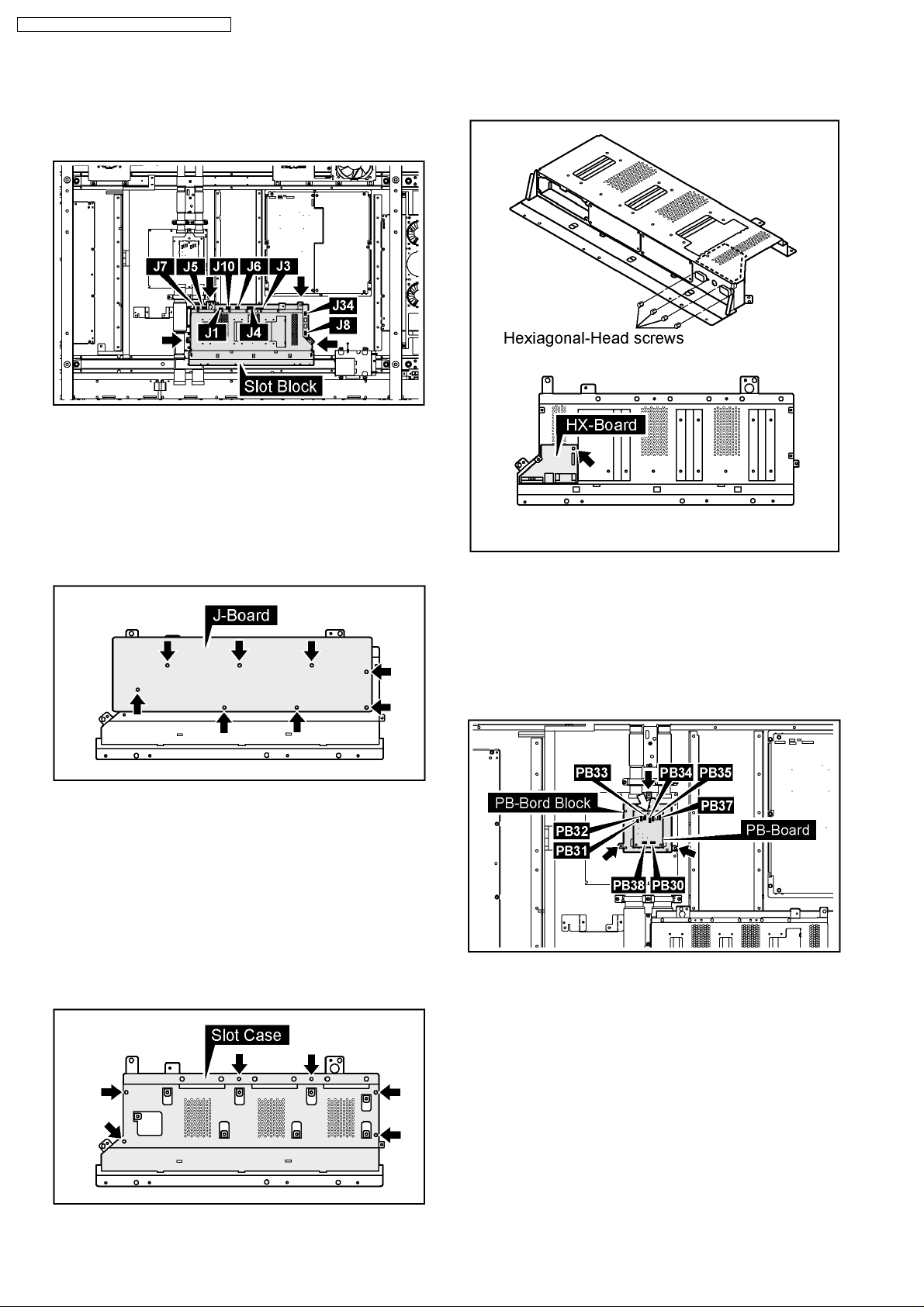
7.3. Removal of the Slot Block
1. Disconnect the couplers(J1, J3, J4, J5, J6, J7, J10, J34).
2. Remove the 4 screws and then remove the Slot Block.
7.4. Removal of the J-Board
1. Remove the HA Terminal Block and the HB Terminal Block.
(Reference to Removal of the HA-Board and the HB-Board)
2. Remove the Slot Block.
(Reference to Removal of the Slot Block)
3. Remove the 8 screws and then remove the J-Board.
5. Remove the 4 Hexagonal-Head screws and the 1 screw of
the HX-Board and then remove the HX-Board.
7.6. Removal of the PB-Board
7.5. Removal of the HX-Board
1. Remove the HA Terminal Block and the HB Terminal Block.
(Reference to Removal of the HA-Board and the HB-Board)
2. Remove the Slot Block.
(Reference to Removal of the Slot Block)
3. Remove the J-Board.
(Reference to Removal of the J-Board)
4. Remove the 6 screws and then remove the Slot Case.
1. Disconnect the couplers(PB30, PB31, PB32, PB33, PB34,
PB35, PB37, PB38).
2. Remove the 3 scewqs and then remove the PB-Board
Block.
3. Remove the 1 screw and then remove the PB-Board.
12
Page 13
TH-65PHD8BK / TH-65PHD8EK / TH-65PHD8UK
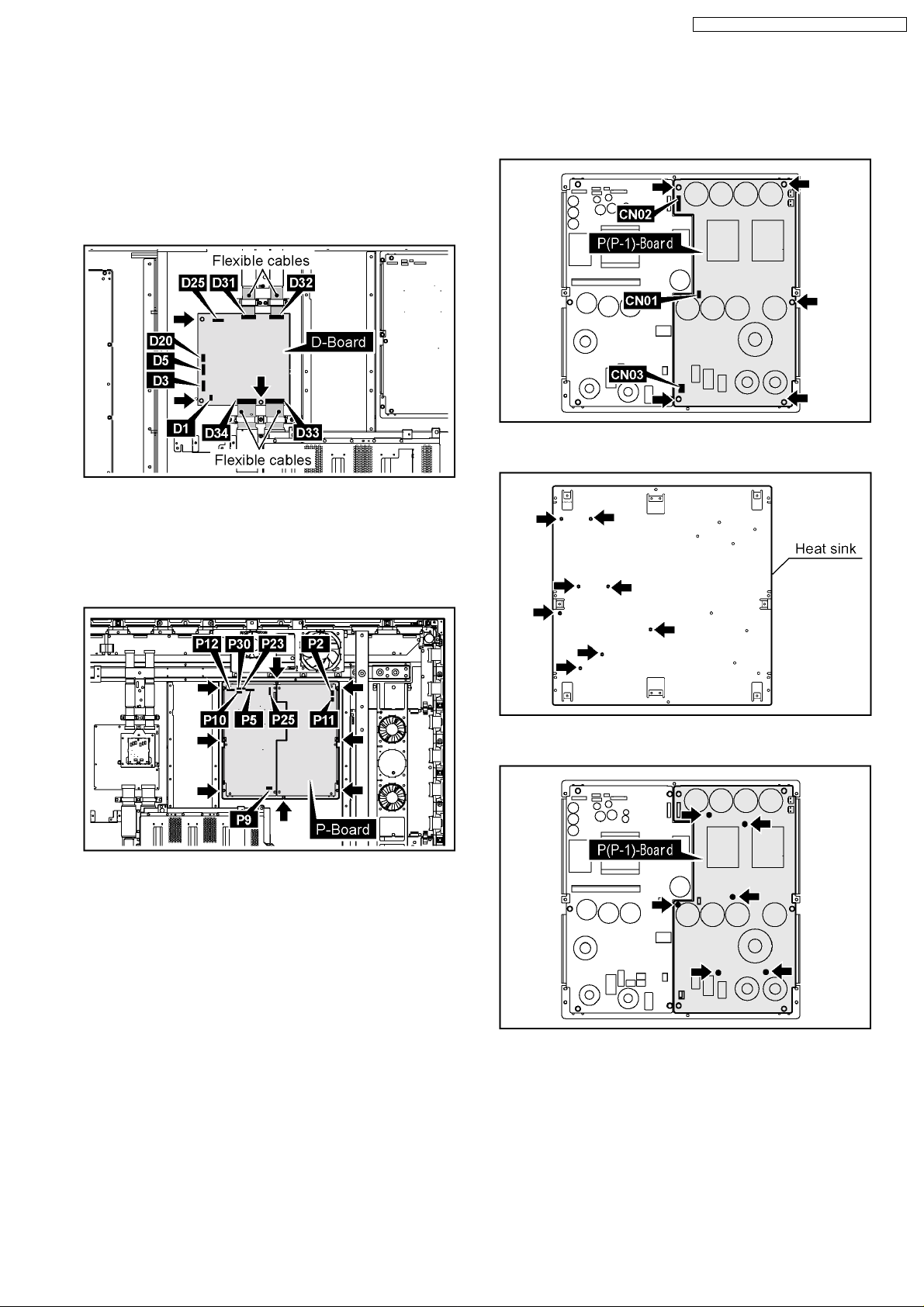
7.7. Removal of the D-Board
1. Remove the PB-Board Block.(Reference to Removal of the
PB-Board)
2. Disconnect the couplers(D1, D3, D5, D20, D25).
3. Remove the flexible cables from the couplers(D31, D32,
D33, D34).
4. Remove the 3 screws and then remove the D-Board.
7.8. Removal of the P-Board
7.8.1. Removal of the P(P-1)-Board
1. Disconnect the couplers(CN01, CN02, CN03).
2. Remove the 5 screws.(Top view)
3. Remove the 8 screws.(Bottom view)
1. Disconnect the couplers(P2, P5, P9, P10, P11, P12, P23,
P25, P30).
2. Remove the 8 screws and then remove the P-Board.
4. Remove the P(P-1)-Board from the 6 molding props.
13
Page 14
TH-65PHD8BK / TH-65PHD8EK / TH-65PHD8UK
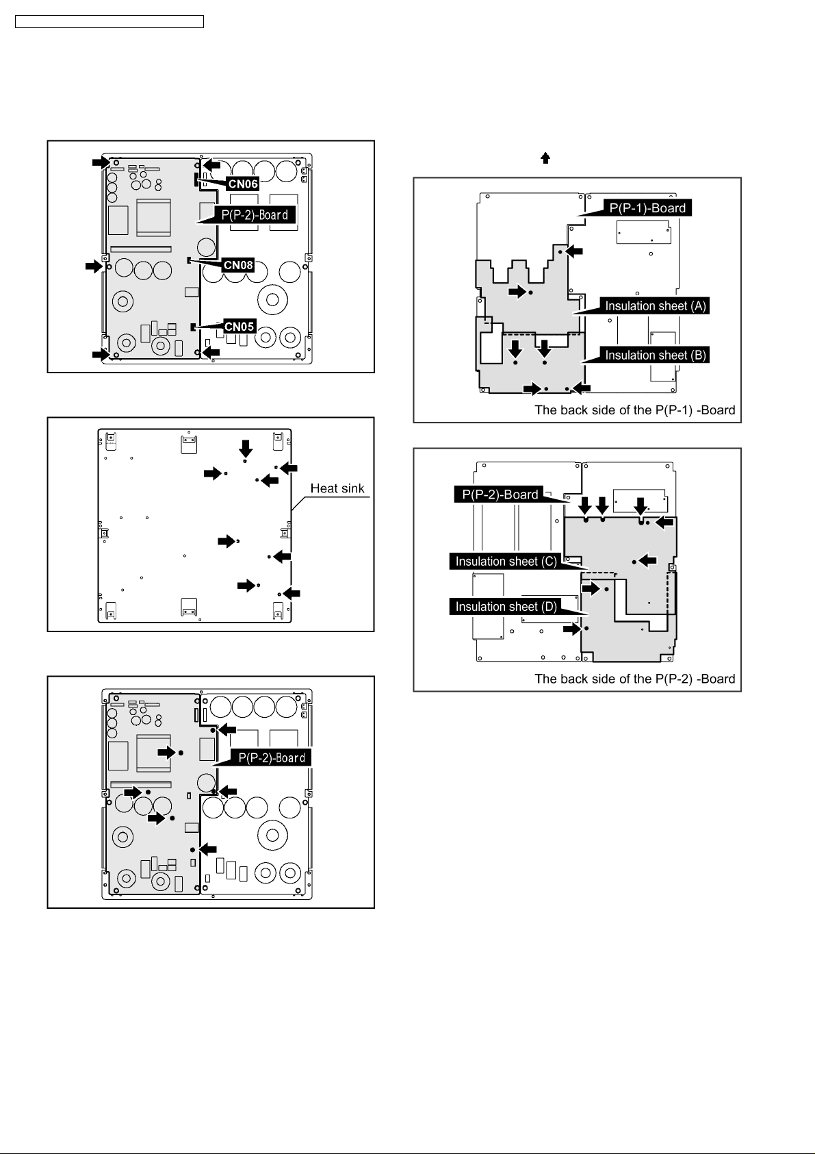
7.8.2. Removal of the P(P-2)-Board
1. Disconnect the couplers(CN05, CN06, CN08).
2. Remove the 5 screws.(Top view)
3. Remove the 8 screws.(Bottom view)
Note:
· When assembling the P(P-1)-Board and the P(P-2)Board, the position of each hole of the insulation
sheets(A, B, C, D) is set to the position of each hole of
the P(P-1)-Board and the P(P-2)-Board and then
assemble them. (
marks indicate setting positions.)
4. Remove the P(P-2)-Board from the 6 molding props.
14
Page 15
TH-65PHD8BK / TH-65PHD8EK / TH-65PHD8UK
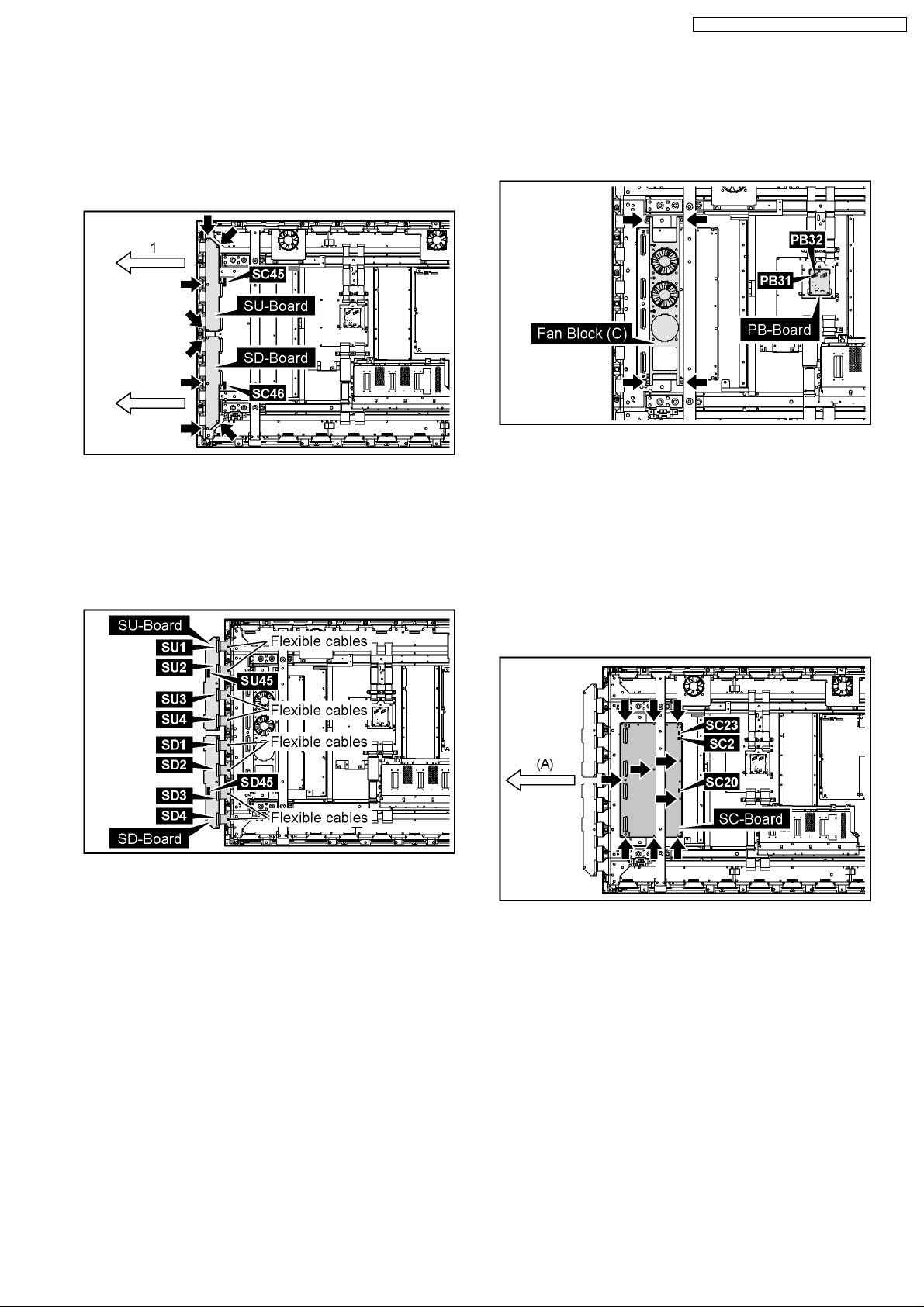
7.9. Removal of the SU-Board and
the SD-Board
1. Disconnect the couplers(SC45, SC46).
2. Remove the each 4 screws.
3. Slide the SU-Board and the SD-Board to the left (arrow1).
4. Disconnect the coupler(SU45).
5. Remove the flexible cables from the couplers(SU1, SU2,
SU3, SU4) and then remove the SU-Board.
6. Disconnect the coupler(SD46).
7. Remove the flexible cables from the couplers(SD1, SD2,
SD3, SD4) and then remove the SD-Board.
7.10. Removal of the SC-Board
1. Disconnect the couplers(PB31, PB32).
2. Remove the each 4 screws and then remove the Fan Block
(C).
3. Slide the SU-Board and the SD-Board to the left.
(Refarence to Removal of the SU-Board and the SD-Board)
4. Disconnect the couplers(SC2, SC20, SC23).
5. Remove the 10 screws of the SC-Board and slide the SCBoard in the direction of the arrow (A) and then remove the
SC-Board.
Note:
Remove the SC-Board not to damage the flexible cables
of the SU-Board and the SD-Board, parts on the SCBoard.
15
Page 16
TH-65PHD8BK / TH-65PHD8EK / TH-65PHD8UK
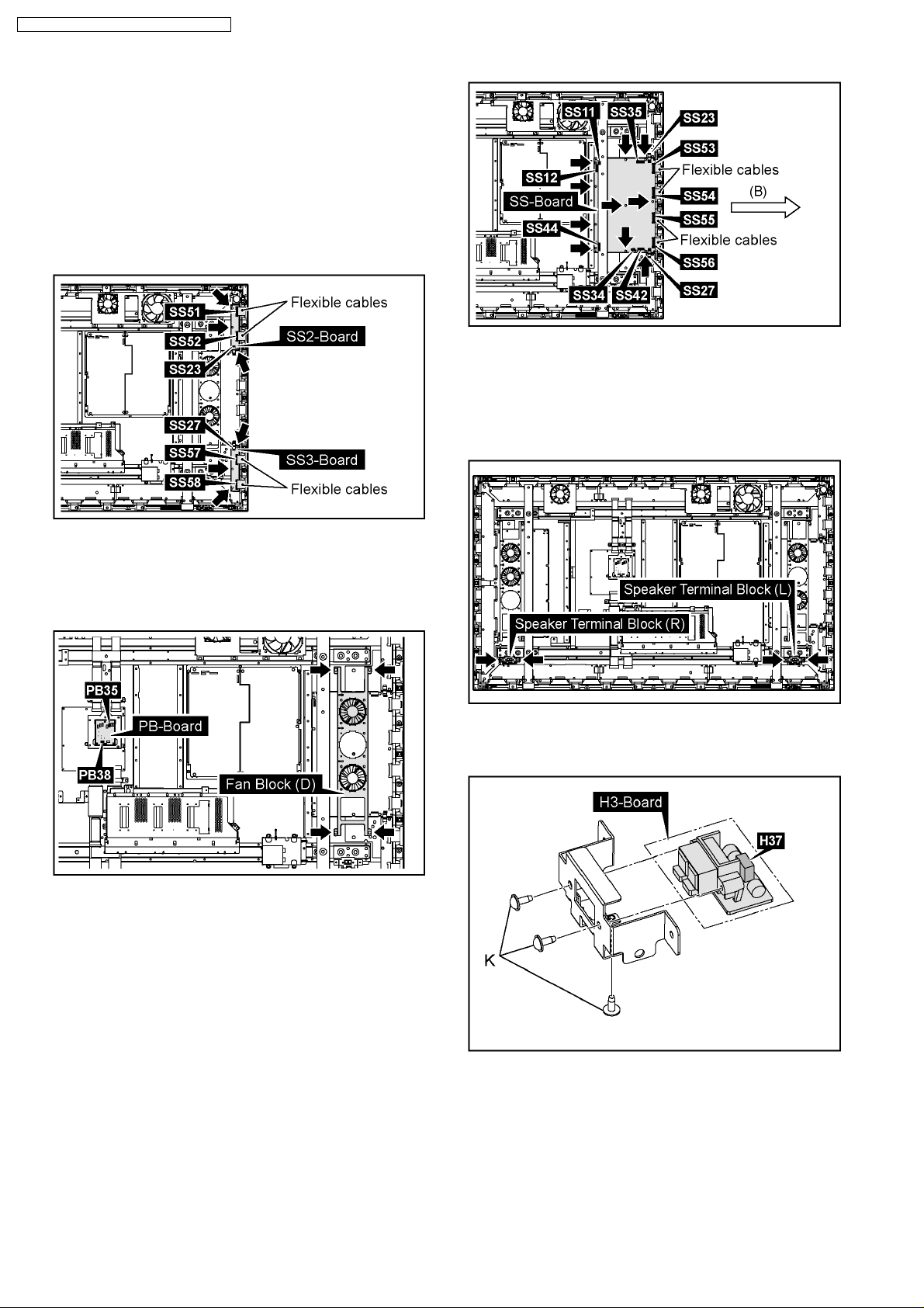
7.11. Removal of the SS2-Board and
the SS3-Board
1. Disconnect the coupler(SS23).
2. Remove the flexible cables from the couplers(SS51, SS52).
3. Disconnect the coupler(SS27).
4. Remove the flexible cables from the couplers(SS57, SS58).
5. Remove the each 3 screws and then remove the SS2-
Board and the SS3-Board.
7.13. Removal of the H3-Board (L,
R)
1. Remove the each 2 screws and then remove the Speaker
Terminal Blocks (L, R).
7.12. Removal of the SS-Board
1. Disconnect the couplers(PB35, PB38).
2. Remove the 4 screws and then remove the Fan Block (D).
3. Disconnect the couplers(SS11, SS12, SS23, SS27, SS34,
SS35, SS42, SS44).
4. Remove the flexible cables from the couplers(SS53, SS54,
SS55, SS56).
5. Remove the 10 screws of the SS-Board and slide the SSBoard in the direction of the arrow (B) and then remove the
SS-Board.
Note:
Remove the SS-Board not to damage the flexible cables
of the Plasma Panel and parts on the SS-Board.
2. Disconnect the coupler(H37).
3. Remove the 3 screws (K) and then remove the H3-Board.
16
Page 17
TH-65PHD8BK / TH-65PHD8EK / TH-65PHD8UK
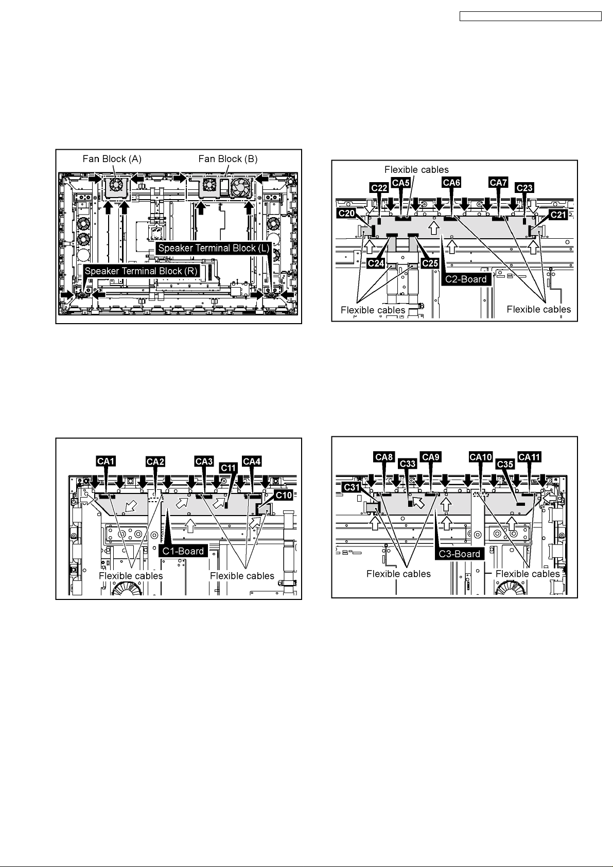
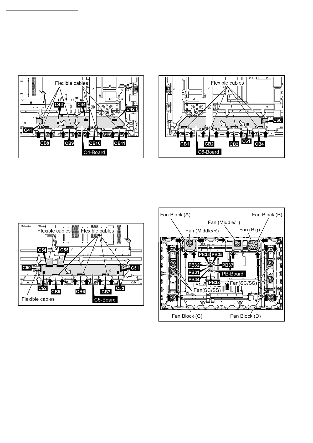
7.14. Removal of the C1, C2, C3, C4,
C5 and the C6-Board
1. Remove the each 4 screws and then remove the Fan
Blocks (A, B).
2. Remove the each 2 screws and then remove the Speaker
Terminal Blocks (L, R).
7.14.1. Removal of the C1-Board
1. Remove the flexible cable from the coupler(C10).
2. Disconnect the coupler(C11).
3. Remove the 8 screws and then remove the flexible cables
from the couplers(CA1, CA2, CA3, CA4).
4. Remove the 6 screws and then remove the C1-Board.
7.14.2. Removal of the C2-Board
1. Remove the flexible cables from the couplers(C20, C21,
C24, C25).
2. Disconnect the couplers(C22, C23).
3. Remove the 6 screws and then remove the flexible cables
from the couplers(CA5, CA6, CA7).
4. Remove the 6 screws and then remove the C2-Board.
7.14.3. Removal of the C3-Board
1. Remove the flexible cable from the coupler(C31).
2. Disconnect the couplers(C33, C35).
3. Remove the 8 screws and then remove the flexible cables
from the couplers(CA8, CA9, CA10, CA11).
4. Remove the 6 screws and then remove the C3-Board.
17
Page 18
TH-65PHD8BK / TH-65PHD8EK / TH-65PHD8UK
7.14.4. Removal of the C4-Board
1. Remove the flexible cable from the coupler(C41).
2. Disconnect the couplers(C42, C43, C44).
3. Remove the 8 screws and then remove the flexible cables
from the couplers(CB8, CB9, CB10, CB11).
4. Remove the 6 screws and then remove the C4-Board.
7.14.5. Removal of the C5-Board
1. Remove the flexible cables from the couplers(C50, C51,
C54, C55).
2. Disconnect the couplers(C52, C53).
3. Remove the 6 screws and then remove the flexible cables
from the couplers(CB5, CB6, CB7).
4. Remove the 6 screws and then remove the C5-Board.
7.14.6. Removal of the C6-Board
1. Remove the flexible cable from the coupler(C60).
2. Disconnect the coupler(C61).
3. Remove the 8 screws and then remove the flexible cables
from the couplers(CB1, CB2, CB3, CB4).
4. Remove the 6 screws and then remove the C6-Board.
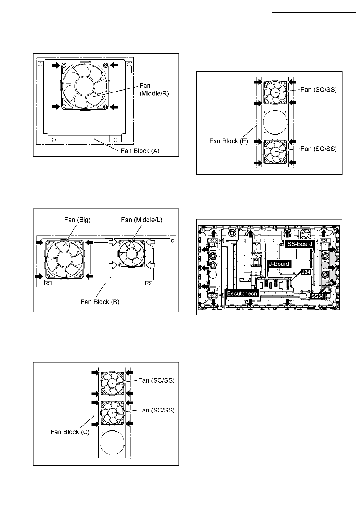
7.15. Removal of the Fan
1. Disconnect the couplers(PB31, PB32, PB33, PB34, PB35,
PB37, PB38).
2. Remove the each 4 screws and then remove the Fan
Blocks(A, B, C, D).
18
Page 19
TH-65PHD8BK / TH-65PHD8EK / TH-65PHD8UK
7.15.1. Removal of the Fan (Middle/R)
1. Remove the 4 screws and then remove the Fan (Middle/R).
7.15.2. Removal of the Fan (Big) and the
Fan (Middle/L)
1. Remove the 4 screws and then remove the Fan (Big).
2. Remove the 4 screws and then remove the Fan (Middle/L).
7.15.4. Removal of the Fan (SC/SS) on the
SS-Board side
1. Remove the each 4 screws and then remove the Fans (SC/
SS).
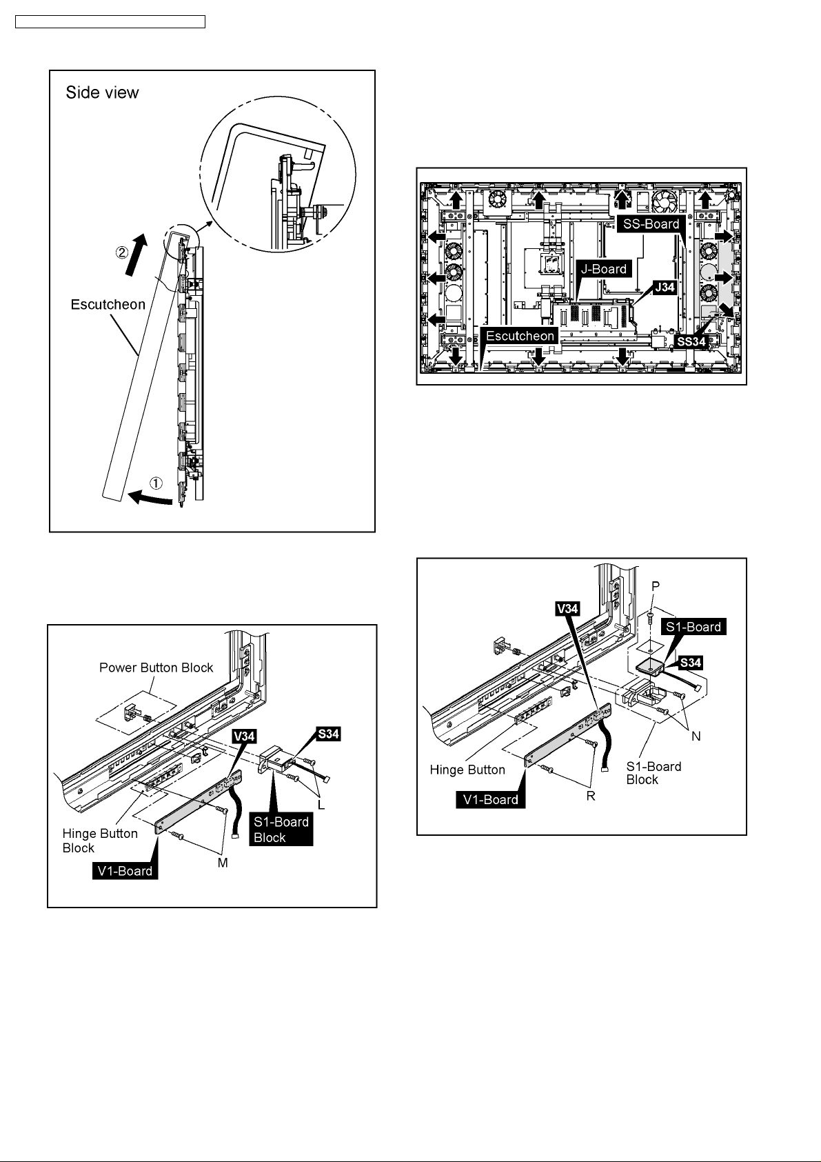
7.16. Removal of the Escutcheon
1. Disconnect the couplers(J34, SS34).
2. Remove the 13 screws.
7.15.3. Removal of the Fan (SC/SS) on the
SC-Board side
1. Remove the each 4 screws and then remove the Fans
(SC/SS).
3. Pull the bottom of the Escutcheon in the direction of the
arrow1 and lift up the Escutcheon in the direction of the
arrow2 and then remove the Escutcheon.
19
Page 20
TH-65PHD8BK / TH-65PHD8EK / TH-65PHD8UK
4. Remove the 2 screws(L) and then remove the S1-Board
Block and then Power Button Block.
5. Remove the 2 screws(M) amd then remove the V1-Board
and the Hinge Button Block.
7.17. Removal of the S1-Board and
the V1-Board
1. Remove the Escutcheon.
(Refernce to Removal of Escutcheon)
2. Remove the 2 screws (N) and then remove the S1-Board
Block.
3. Remove the 1 screw (P) and then remove the S1-Board.
4. Remove the 2 screws (R) and then remove the V1-Board.
5. Disconnect the coupler(S34) and then remove the S1-
Board.
6. Disconnect the coupler(V34) and then remove the V1-
Board.
20
Page 21
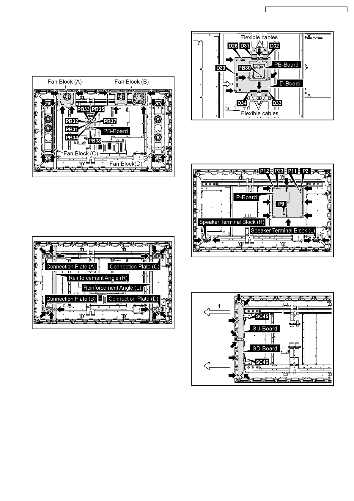
7.18. Removal of the Plasma Panel
1. Disconnect the couplers(PB31, PB32, PB33, PB34, PB35,
PB37, PB38).
2. Remove the each 4 screws and then remove the Fan
Blocks(A, B, C, D).
TH-65PHD8BK / TH-65PHD8EK / TH-65PHD8UK
9. Disconnect the couplers(P2, P9, P11, P12, P23).
10. Remove the 8 screws and then remove the P-Board.
11. Remove the each 2 screws and then remove the Speaker
Terminal Blocks (L, R).
3. Remove the each 2 screws and then remove the
Reinforcement Angles (L, R).
4. Remove the each 2 screws and then remove the
Connection Plate (A, B, C, D).
5. Remove of the Slot Block.
(Reference to Removal of the Slot Block).
6. Disconnect the couplers(D20, D25, PB30).
7. Remove the flexible cables from the couplers(D31, D32,
D33, D34).
8. Remove the 7 screws and then remove the PB-Board Block
and D-Board.
12. Disconnect the couplers(SC45, SC46).
13. Remove the each 4 screws and then slide the SU-Board
and the SD-Board to the left (arrow 1).
14. Remove the flexible cables from the couplers(SU1, SU2,
SU3, SU4, SD1, SD2, SD3, SD4) and then remove the SUBoard and the SD-Board.
21
Page 22
TH-65PHD8BK / TH-65PHD8EK / TH-65PHD8UK
15. Remove the 10 screws and then remove the SC-Board.
22. Disconnect the couplers(C11, C33).
23. Remove the flexible cables from the couplers(C10, C21,
C24, C25).
24. Remove the each 6 screws and then remove the C1-Board,
the C2-Board and the C3-Board.
16. Remove the SS2-Board and the SS3-Board.
(Reference to Removal of the SS2-Board and the SS3-
Board).
17. Disconnect the couplers(SS34, SS35, SS42, SS44).
18. Remove the flexible cables from the couplers(SS53, SS54,
SS55, SS56).
19. Remove the 10 screws and then remove the SS-Board.
20. Remove the 22 screws.
21. Remove the flexible cables from the couplers(CA1, CA2,
CA3, CA4, CA5, CA6, CA7, CA8, CA9, CA10, CA11).
25. Remove the 22 screws.
26. Remove the flexible cables from the couplers(CB1, CB2,
CB3, CB4, CB5, CB6, CB7, CB8, CB9, CB10, CB11).
27. Disconnect the couplers(C43, C61).
28. Remove the flexible cables from the couplers(C41, C50,
C54, C55).
22
Page 23
TH-65PHD8BK / TH-65PHD8EK / TH-65PHD8UK
29. Remove the each 6 screws and then remove the C4-Board,
the C5-Board and the C6-Board.
30. Remove the each 2 screws and then remove the Shield
Plate and the Angle.
31. Remove the 4 screws and then remove the AC Inlet Block.
arrow2 and then remove the Plasma Panel.
32. Remove the each 2 screws and then remove the Shield
Plates (A, B).
33. Remove the each 3 screws and then remove the Cable
Holders (A, B) and the flexible cables.
34. Remove the 13 screws of the Escutcheon.
35. Lift up the bottom of the Plasma Panel in the direction of the
arrow1 and pull the Plasma Panel in the direction of the
23
Page 24
TH-65PHD8BK / TH-65PHD8EK / TH-65PHD8UK
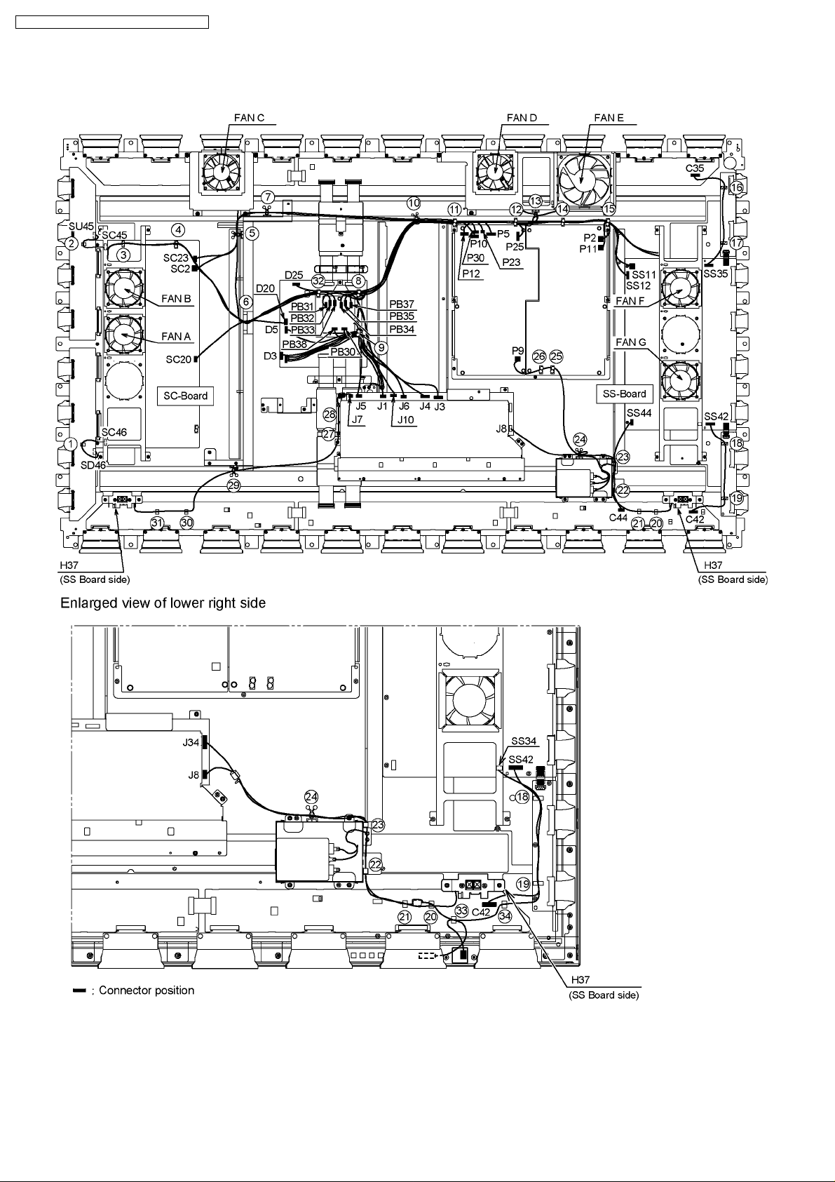
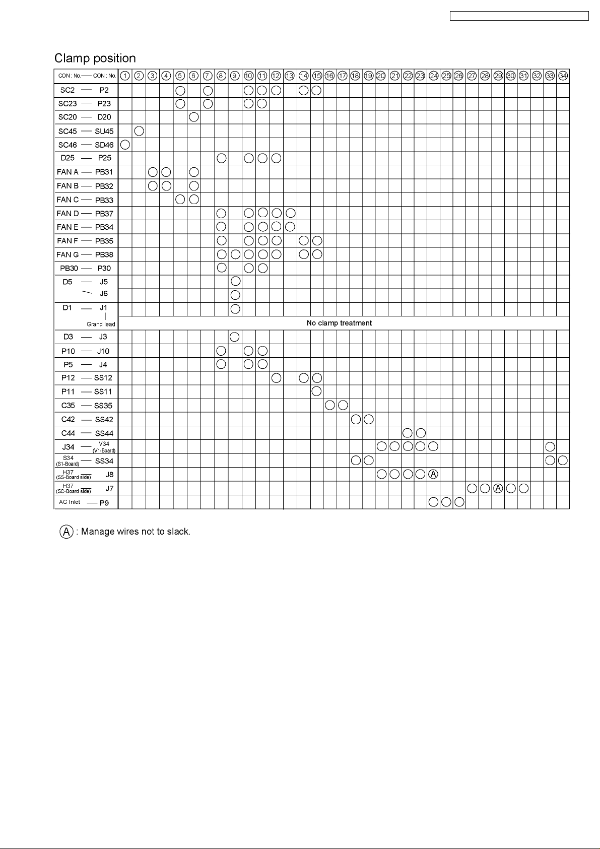
8 Location of Lead Wiring
24
Page 25
TH-65PHD8BK / TH-65PHD8EK / TH-65PHD8UK
25
Page 26
TH-65PHD8BK / TH-65PHD8EK / TH-65PHD8UK
9 Adjustment Procedure
9.1. Driver Set-up
9.1.1. Item / Preparation
1. Input a white signal of the RGB signal generator.
2. Set the picture adjustment items as follows.
· Picture menu : Standard
· Color temperature : Normal
· Picture : 25
· Aspect : Full
9.1.2. Adjustments
Adjust driver section voltages referring the panel data on the panel data label.
Caution
1. First perform Vsus voltage adjustment.
2. Confirmation of Vscn voltage should be performed after confirmation of Vad voltage adjustment.
When Vad = -85V, Voltage of Vscn is 35V ± 4V.
26
Page 27
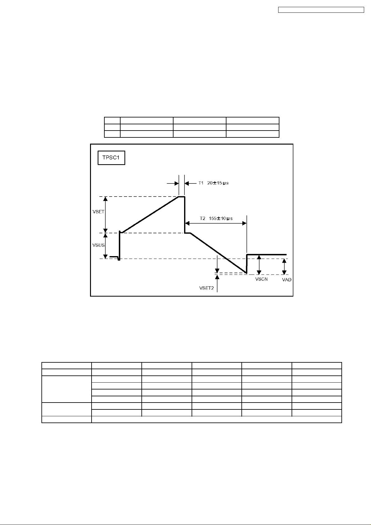
9.2. Initialization Pulse Adjust
1. Input a white signal to plasma video input.
2. Set the picture adjustment items as follows.
· Picture menu : Standard
· Color temperature : Normal
· Picture : 25
· Aspect : Full
3. Connect Oscilloscope to TPSC1 (T1) and check for 20 ± 15µ Sec.
4. Connect Oscilloscope to TPSC1 (T2) and adjust VR6602 for 155 ± 10µ Sec.
Test point Volume Level
T1 TPSC1 (SC) Fixed 20 ± 15µ Sec
T2 TPSS1 (SS) VR6602(SC) 155 ± 10µ Sec
TH-65PHD8BK / TH-65PHD8EK / TH-65PHD8UK
9.3. P.C.B. (Printed Circuit Board) Remove
9.3.1. Caution
1. To remove P.C.B., wait 1 minute after power was off for discharge from electrolysis capacitors.
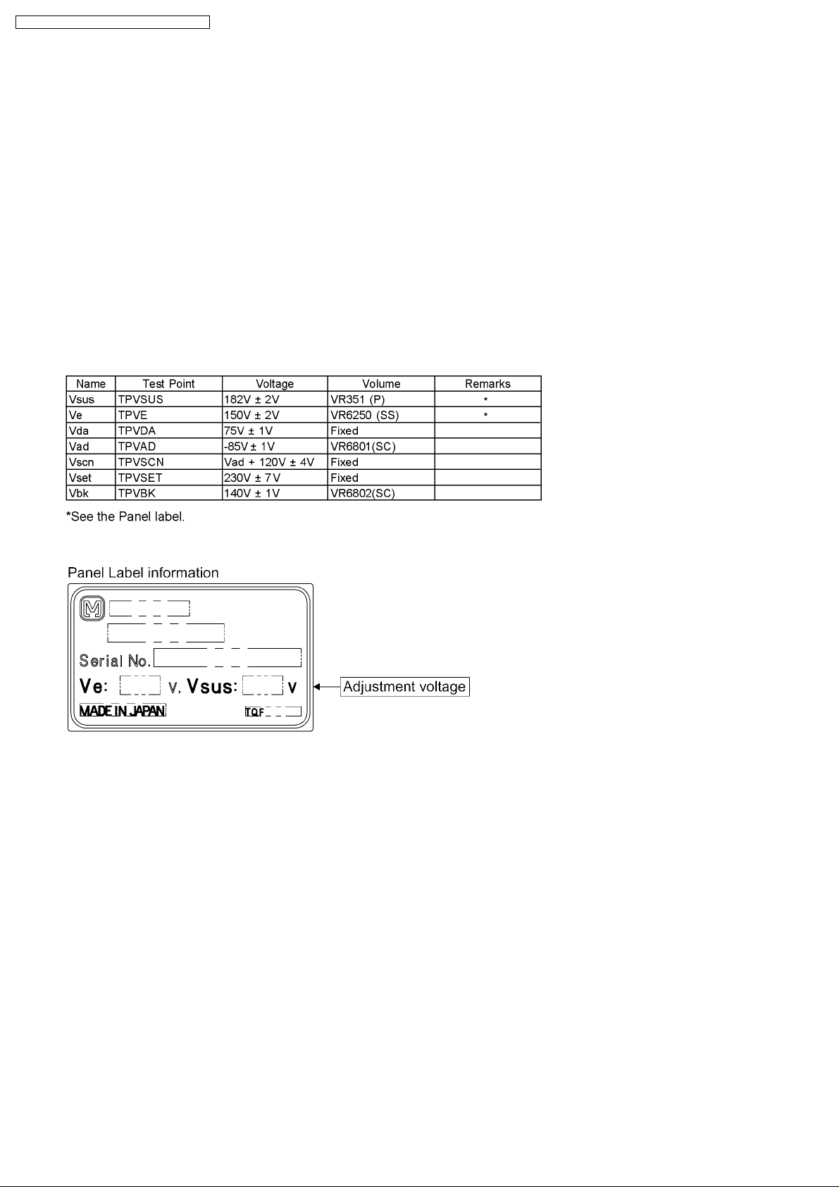
9.3.2. Quick adjustment after P.C.B. Remove
P.C.B. Name Test Point Voltage Volume Remarks
P Board Vsus TPVSUS 182V ± 2V VR351 (P) *
SC Board Vad TPVAD -85V ± 1V VR6801 (SC)
Vscn TPVSCN Vad + 120V ± 4V Fixed
Vset TPVSET 230V ± 7V Fixed
Vbk TPVBK 140V ± 1V VR6802 (SC)
SS Board Ve TPVE 150V ± 2V VR6250 (SS) *
Vda TPVDA 75V ± 1V Fixed
D, J Board White balance, Pedestal and Sub brightness for NTSC, PAL, HD, PC and 625i signals
*See the Panel label.
Caution:
Absolutely do not reduce Vsus below Ve not to damage the P.C.B.
27
Page 28
TH-65PHD8BK / TH-65PHD8EK / TH-65PHD8UK
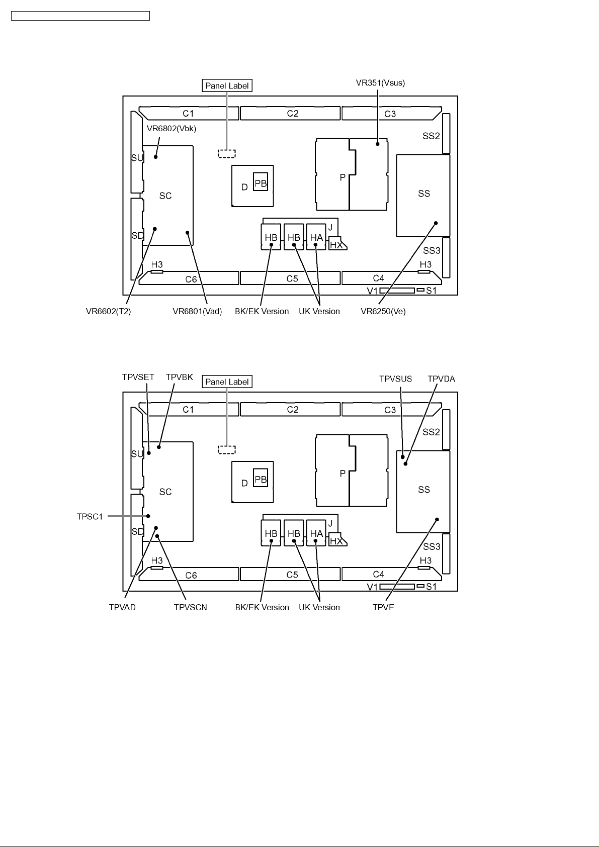
9.4. Adjustment Volume Location
9.5. Test Point Location
28
Page 29
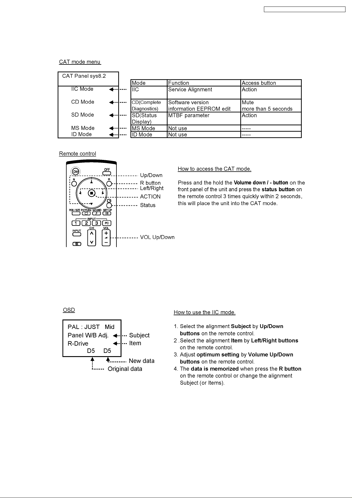
10 Service mode
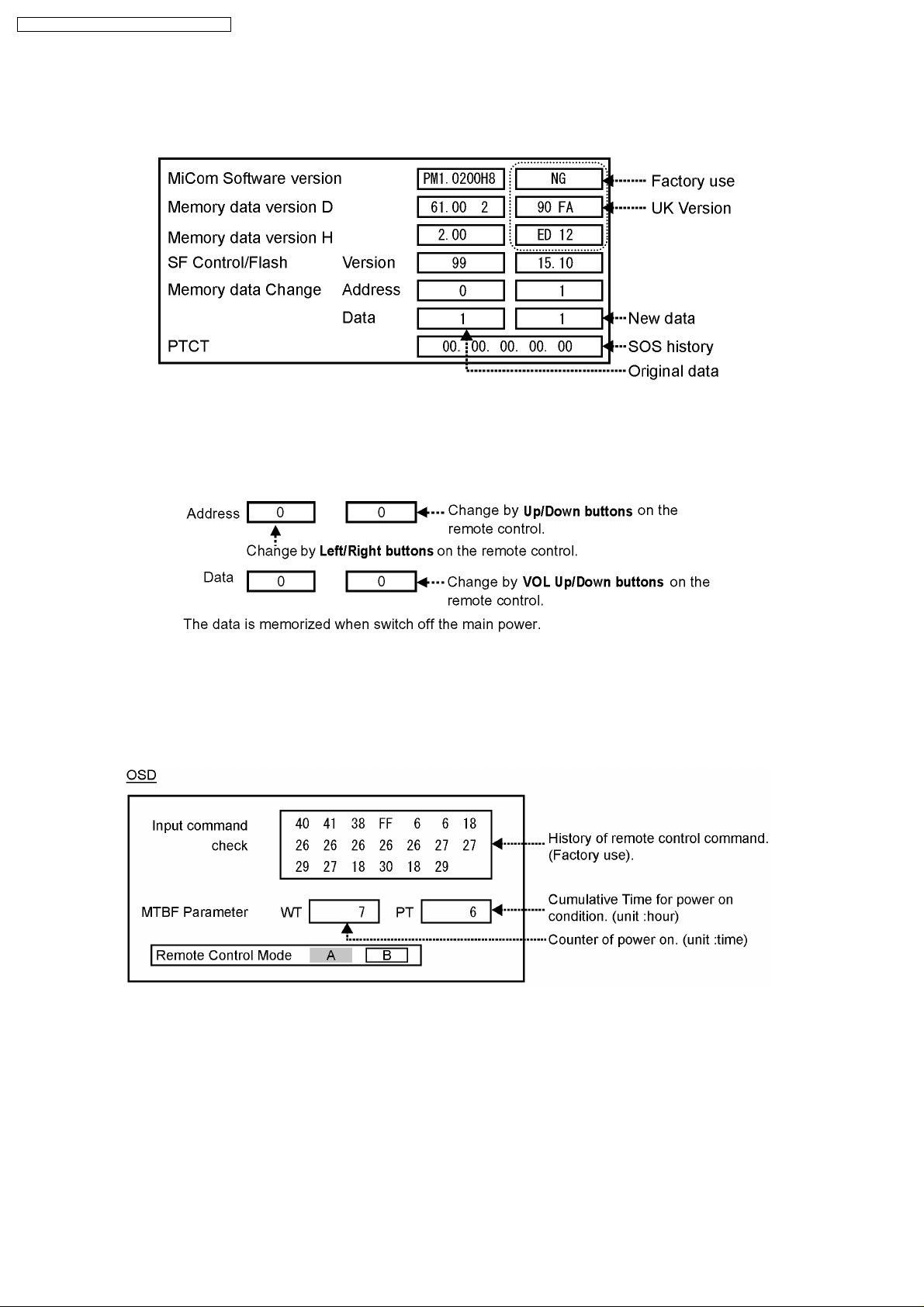
10.1. CAT (computer Aided Test) mode
TH-65PHD8BK / TH-65PHD8EK / TH-65PHD8UK
To exit the CAT mode, access the ID mode and switch off the main power.
10.1.1. IIC mode
Select the IIC mode by Up/Down button on the remote control at the front page of CAT mode and then press the Action button
on the remote control.
Subject and item are mentioned on “IIC mode structure”.
To exit the IIC mode, press the R button on the remote control.
29
Page 30
TH-65PHD8BK / TH-65PHD8EK / TH-65PHD8UK
10.1.2. CD mode
Select the CD mode by Up/Down button on the remote control at the front page of CAT mode and then press the Mute button
on the remote control more than 5 seconds.
Micom software version (IC9702), this version can be upgrade by
1. replace of new version IC
2. Loading the new version software from loader tool, TZSC07036.
Memory data change
To exit the CD mode, press the R button on the remote control.
10.1.3. SD mode
Select the SD mode by Up/Down button on the remote control at the front page of CAT mode and then press the Action button
on the remote control.
To exit the SD mode, press the R button on the remote control.
30
Page 31

TH-65PHD8BK / TH-65PHD8EK / TH-65PHD8UK
10.2. IIC mode structure (following items value is sample data.)
31
Page 32

TH-65PHD8BK / TH-65PHD8EK / TH-65PHD8UK
11 Alignment
11.1. PC / RGB panel white balance
INPUT Alignment menu ProcedureEquipment Setting
1 PC (VGA) Color
Gray Scale Analyzer
Pattern
High light 75%
Low light 15%
Picture menu:
Standard
Picture:
25
Color temperature:
Cool
Aspect:
Full
POS./Size:
Normal
Component/
RGB-IN Select:
RGB
IIC mode:
Panel W/B Adj
Note: · Before adjustment, color signal has not been displayed
on panel.
· The pedestal adjustment has been done.
PANEL W/B
G cut off
PANEL W/B
G Drive 3) Set G Drive to " E0 ".
PANEL W/B
B Drive 4) Adjust B and R Drive to set the High color temperature
R Drive as shown Table 1.
PANEL W/B
R,G,B Drive 5) Increase equaly R, G and B Drive to get the
· The signal root must be A side.
1) Set G cut off to " 80 ".
2)Find 75% (amplitude) of white area by color sensor.
largest level of 3 color drive to "FC".
Color Temp. x y
Cool(Hi) 0.276 0.276
Normal(Mid) 0.288 0.296
Warm(Low) 0.313 0.329
Table 1 W/B adjustment values
2 1) Change color temperature to "Normal".
3 1) Change color temperature to "Warm".
· NTSC
4 1) Copy the R drive, G drive and B drive data obtained in above
· PAL
· DVI
Picture menu:
Standard
Picture:
25
Color temperature:
Normal
Aspect:
Full
POS./Size:
Normal
Picture menu:
Standard
Picture:
25
Color temperature:
Warm
Aspect:
Full
POS./Size:
Normal
PANEL W/B
PANEL W/B
R,G,B Drive
PANEL W/B
PANEL W/B
R,G,B Drive
G cut off 2) In Mid color temperature, repeat the procedures 1) to 5) of
Cool mode.
G cut off 2) In Low color temperature, repeat the procedures 1) to 5) of
Cool mode.
steps into NTSC, PAL and DVI area.
32
Page 33

TH-65PHD8BK / TH-65PHD8EK / TH-65PHD8UK
Color temperature
High
Medium
Low
R
A0-11AD
A0-11B0
A0-11B3
G
A0-11AE
A0-11B1
A0-11B4
Table 2 Drive data addresses (PC/RGB)
Color temperature
High
Medium
Low
R
A0-1180
A0-1183
A0-1186
G
A0-1181
A0-1184
A0-1187
Table 3 Drive data addresses (NTSC)
Color temperature
R
G
B
A0-11AF
A0-11B2
A0-11B5
B
A0-1182
A0-1185
A0-1188
B
High
Medium
Low
A0-1189
A0-118C
A0-118F
A0-118A
A0-118D
A0-1190
Table 4 Drive data addresses (PAL)
Color temperature
High
Medium
Low
R
A0-11B6
A0-11B9
A0-11BC
A0-11B7
A0-11BA
A0-11BD
Table 5 Drive data addresses (DVI)
A0-118B
A0-118E
A0-1191
G
B
A0-11B8
A0-11BB
A0-11BE
33
Page 34

TH-65PHD8BK / TH-65PHD8EK / TH-65PHD8UK
11.2. HD / 525ip / 625ip panel white balance
INPUT Alignment menu ProcedureEquipment Setting
1 Color
HD
(YUV2_HD)
Gray Scale
Pattern
High light 75%
Low light 15%
Analyzer
Picture menu:
Standard
Picture:
25
Color temperature:
Cool
Aspect:
Full
POS./Sise:
Normal
Component/
RGB-IN Select:
COMPONENT
IIC mode:
Panel W/B Adj
Note: · Before adjustment, color signal has not been displayed
on panel.
· The pedestal adjustment has been done.
PANEL W/B
G cut off
PANEL W/B
G Drive 3) Set G Drive to " E0 ".
PANEL W/B
B Drive 4) Adjust B and R Drive to set the High color temperature
R Drive as shown Table 1.
PANEL W/B
R,G,B Drive 5) Increase equaly R, G and B Drive to get the
· The signal root must be A side.
1) Set G cut off to " 80 ".
2)Find 75% (amplitude) of white area by color sensor.
largest level of 3 color drive to "FC".
Color Temp. x y
Cool(Hi) 0.276 0.276
Normal(Mid) 0.288 0.296
Warm(Low) 0.313 0.329
Table 1 W/B adjustment values
2 1) Change color temperature to "Normal".
3 1) Change color temperature to "Warm".
· YUV1_525ip
4 1) Copy the R drive, G drive and B drive data obtained in above
· YUV3_625ip
Picture menu:
Standard
Picture:
25
Color temperature:
Normal
Aspect:
Full
POS./Sise:
Normal
Picture menu:
Standard
Picture:
25
Color temperature:
Warm
Aspect:
Full
POS./Sise:
Normal
PANEL W/B
PANEL W/B
R,G,B Drive
PANEL W/B
PANEL W/B
R,G,B Drive
G cut off 2) In Mid color temperature, repeat the procedures 1) to 5) of
Cool mode.
G cut off 2) In Low color temperature, repeat the procedures 1) to 5) of
Cool mode.
steps into YUV1_525ip, YUV3_625ip area.
34
Page 35

TH-65PHD8BK / TH-65PHD8EK / TH-65PHD8UK
Color temperature
High
Medium
Low
R
A0-119B
A0-119E
A0-11A1
G
A0-119C
A0-119F
A0-11A2
Table 2 Drive data addresses (YUV2_HD)
Color temperature
High
Medium
Low
R
A0-1192
A0-1195
A0-1198
G
A0-1193
A0-1196
A0-1199
Table 3 Drive data addresses (YUV1_525ip)
B
A0-119D
A0-11A0
A0-11A3
B
A0-1194
A0-1197
A0-119A
Color temperature
High
Medium
Low
R
A0-11A4
A0-11A7
A0-11AA
G
A0-11A5
A0-11A8
A0-11AB
Table 4 Drive data addresses (YUV3_625ip)
B
A0-11A6
A0-11A9
A0-11AC
35
Page 36

TH-65PHD8BK / TH-65PHD8EK / TH-65PHD8UK
12 Trouble shooting guide
12.1. Self Check
12.1.1. Display Indication
1. Self-check is used to automatically check the bus line
controlled circuit of the Plasma display.
2. To get into the Self-check mode, press the volume down
button on the customer controls at the bottom of the set, at
the same time pressing the OFF-TIMER button on the
remote control, and the screen will show :-
If the CCU ports have been checked and found to be incorrect
Or not located then " - - " will appear in place of " OK "
“ 01 “ in the line of the “ PTCT ” means the number of blinks of
the Power LED is 1. (Reference to 12.1.2)
“ H09 “ in the line of the “ PTCT ” is the error code.
Note:
The line of the “ PTCT ” displays when you get into the Selfcheck mode for the first time only after the Power LED
blinks.
12.1.2. Power LED Blinking timing chart
1. Subject
Information of LED Blinking timing chart.
2. Contents
When an abnormality has occurred the unit, the protection circuit operates and reset to the stand by mode. At this time, the
defective block can be identified by the number of blinkes of the Power LED on the front panel of the unit.
3. Remarks
Above Fan function is operated during the fans are installed.
36
Page 37

12.2. No Power
First check point
1. No lit.
2. Green is lit then turns red blinking a few seconds later.
3. Only red is lit.
1. No lit.
TH-65PHD8BK / TH-65PHD8EK / TH-65PHD8UK
12.3. No Picture
37
Page 38

TH-65PHD8BK / TH-65PHD8EK / TH-65PHD8UK
12.4. Local screen failure
Plasma display may have local area failure on the screen. Fig - 1 is the possible defect P.C.B. for each local area.
Fig - 1
38
Page 39

13 Option Setting
TH-65PHD8BK / TH-65PHD8EK / TH-65PHD8UK
39
Page 40

TH-65PHD8BK / TH-65PHD8EK / TH-65PHD8UK
Option Menu for GPH8D series
GPH8D chassis series have special function and operation setting facility called Option Menu. This Option Menu is useful for
special function required customers. This should be set at the installation stage.
Option menus default setting Contents
Off-timer function Enable Off-timer operation Enable/Disable.
Onscreen display On Enable/Disable to display input mode indication after power on and no signal
Initial INPUT Off Sets the initial input mode when the power is turned on. Allow input mode
Initial VOL level Off Sets the initial volume level when the power is turned on. Allow Volume
Maximum VOL Level Off Sets the maximum volume to desired level. Volume cannot exceed this level.
INPUT lock Off Fixes the input mode to AV, Component/RGB or PC. Can not change input
Studio W/B Off Set warm mode color temperature to 3,200 Kelvin.
Advanced PIP Off Off : Sets normal two screen display mode.
Display size Off Adjusts the image display size on screen.
Button lock Off Enable/Disable bottom operation buttons (Input, Menu, Enter and/or volume
Remocon User Level Off Remote key invalidation.
ID select 0 Set ID number from 0 to 100.
Remote ID Off Remote ID function On/Off.
Serial ID Off Serial ID function On/Off
Slot power Off Sets the slot power mode while the power is turned on.
V. Installation Off V. Installation function On/Off
Rotate Off The image rotates 180 degrees (up-down)
indication.
selection while power is on.
control while power is on.
mode by input selection key.
On : Sets Advanced PIP mode.
On : Sets the image display size approximately 95% of the normal image
display.
up/down)
Off : Valid key is all key of remote.
User1 : Valid key are only Stand-by (ON/OFF), Input, Direct input, Status,
Surround, Sound mute On/Off, and volume adjustment.
User2 : Valid key is only Stand-by (ON/OFF).
User3 : All keys are null and void
(While the Remote ID on, standard remote function can not control the unit.)
Allow Optional Terminal Board insert Slots while power is on.
This mode is available for TH-65PHD8BK/EK/UK.
Note: Turn up the power switch for the upward direction when you set display
vertically.
Note :
When both main unit buttons and remote control are disabled due to the “Button lock”, “Remocon User level” or “RemoteID”
adjustments, set all the values “Off” so that all the buttons are enabled again.
Press the “Volume down” button on main unit together with “R“ button on the remote control and hold for more than 5 seconds.
The “SHIPPING” menu is displayed and the lock is released when it disappears.
40
Page 41

14 Circuit Board Layout
14.1. P-Board (P-1), (P-2)
6
P(P-1)-BOARD (FOIL SIDE)
5
ETXMM584MEK (NPX584ME-1)
TH-65PHD8BK / TH-65PHD8EK / TH-65PHD8UK
P-1
4
3
Parts Location
P-BOARD (FOIL SIDE)
IC
MC301 D-2
MC302 D-4
MC303 B-4
MC601 E-4
MC602 E-4
MC604 D-2
MC605 F-4
2
TRANSISTOR
Q332 D-4
Q333 C-4
Q602 E-4
Q603 E-4
Q605 E-3
Q606 E-3
TP
TP1 D-2
TP2 D-2
1
TH-65PHD8 SERIES
P-BOARD ETXMM584MEK
ABCDEFGH I
TH-65PHD8 SERIES
P-BOARD ETXMM584MEK
41
Page 42

TH-65PHD8BK / TH-65PHD8EK / TH-65PHD8UK
6
P(P-1)-BOARD (COMPONENT SIDE)
5
ETXMM584MEK (NPX584ME-1)
P-1
4
3
Parts Location
P-BOARD (COMPONENT SIDE)
IC
MC301 D-2
MC302 D-4
MC303 E-4
MC601 B-4
MC602 B-4
MC604 C-2
MC605 B-4
TP
TP1 C-2
TP2 C-2
2
1
TH-65PHD8 SERIES
P-BOARD ETXMM584MEK
ABCDEFGH I
TH-65PHD8 SERIES
P-BOARD ETXMM584MEK
42
Page 43

TH-65PHD8BK / TH-65PHD8EK / TH-65PHD8UK
6
P-2
P(P-2)-BOARD (FOIL SIDE)
5
ETXMM584MEK (NPX584ME-2)
4
Parts Location
P-BOARD (FOIL SIDE)
3
IC
IC401 C-4
IC701 C-4
IC901 C-2
MC401 C-3
MC701 C-4
MC801 B-3
MC901 D-3
MC902 C-3
MC1601 D-3
MC1602 E-4
MC1604 F-4
2
TRANSISTOR
Q402 C-3
Q451 B-4
Q452 A-4
Q453 B-4
Q454 A-4
Q703 C-5
Q951 B-2
Q952 B-2
Q953 B-3
Q954 B-2
Q955 B-3
Q956 B-3
Q1601 E-3
Q1602 E-4
Q1603 E-4
Q1605 E-4
Q1606 E-4
1
TH-65PHD8 SERIES
P-BOARD ETXMM584MEK
ABCDEFGH I
TH-65PHD8 SERIES
P-BOARD ETXMM584MEK
43
Page 44

TH-65PHD8BK / TH-65PHD8EK / TH-65PHD8UK
6
P(P-2)-BOARD (COMPONENT SIDE)
5
ETXMM584MEK (NPX584ME-2)
P-2
4
Parts Location
P-BOARD (COMPONENT SIDE)
3
IC
IC401 D-4
IC701 D-4
IC901 E-2
MC401 E-3
MC701 E-4
MC801 F-3
MC901 C-3
MC902 E-3
MC1601 C-3
MC1602 B-3
MC1604 B-4
TRANSISTOR
Q1601 C-3
2
1
TH-65PHD8 SERIES
P-BOARD ETXMM584MEK
ABCDEFGH I
TH-65PHD8 SERIES
P-BOARD ETXMM584MEK
44
Page 45

14.2. PB-Board
6
5
Parts Location
PB-BOARD (FOIL SIDE)
IC
IC850 C-2 Q850 B-3
TRANSISTOR
TP
TPFAN B-2
Parts Location
PB-BOARD (COMPONENT SIDE)
IC
IC850 G-3 Q850 G-3
TRANSISTOR
TH-65PHD8BK / TH-65PHD8EK / TH-65PHD8UK
PB
4
3
2
PB-BOARD (FOIL SIDE)
TNPA3655AB
R851
C851
Q850
C
E
R853
5
R864
1
PB38
PB30
13
R860
L852
D856
C852
JS852
C853
TPFAN
C854
R850
R863
D859
TNPA3655
SEE REVERSE FOR ORDER NO.
B
D860
D858
JS851
R852
4
IC850
C850
1
L851
1
R862
R858
5
2
PB
D855
3
D852
R855
D851
D850
D857
D854
D853
R854
PbF
R857
R861
3
3
R859
3
R856
3
3
PB-BOARD (COMPONENT SIDE)
TNPA3655AB
1
3
PB35
PB37
PB36
1
3
3
1
1
3
1
1
3
PB36PB37
1
3
PB35
1
PB34
1
1
PB32PB33
1
PB31
1
PB32 PB33
1
PB31
3
1
R861
PB34
3
3
R854
TNPA3655
ORDER
D857
R859
D855
R858
D854
R857
D853
R856
D852
R855
D851
D850
NO.
J2
C850
3
L851
JS851
D858
R852
R862
5
2
PB
R863
4
IC850
1
D860
D859
C854
J101
R850
C852
1
C853
Q850
J1
D856
R851
JS852
R860
L852
C851
R853
5
R864
1
PB30
13
PB38
1
TH-65PHD8 SERIES
PB-BOARD TNPA3655AB
ABCDEFGH I
TH-65PHD8 SERIES
PB-BOARD TNPA3655AB
45
Page 46

TH-65PHD8BK / TH-65PHD8EK / TH-65PHD8UK
14.3. HA-Board
6
5
HA-BOARD(FOIL SIDE)
TXNHA10RBS
HA
TNPA2845
A1
ORDER
NO.
A2
B1
B2
4
1
IC002
8
PbF
CR NO.3
4
5
3
2
JK002
LR
Pr
1
A39
A40
B39
H1
JK001
Pb
B40
Y
HA-BOARD(COMPONENT SIDE)
TXNHA10RBS
CR NO.3
R043
PbF
JS001
HA
TNPA2845
SEE REVERSEFOR ORDERNO.
JS002
1
JS003
C001
A39
A40
B39
B40
TP032
Y
R038
JS014
C017
C016
C020
C019
R029
R020
R021
C009
R009
R046 R047
C024
C002
C003
NP
JS011
L001
R001
YPb
JS015
R044
R008
R002
R039
R034
R010 R011
C025
TP034
TP033
Pr
Pb
JS016
C015
C014
R035
16
9
8
1
IC001
C013
C005
C004
NP
JS012
R003
L002
R045
C026
R040
R032
R030
TP035
RL
L007
R031
R012
JS013
JK001
TP036
H1
C022
R041
R042
C018
JS004
R028
JS005
R024
R027
R033
JS006
R013
C010
R048
C006
NP
L003
Pr
HA
(UK)
A1
A2
B1
B2
JS009
C023
L006
C011
R025
Q001
R016
R017
R007
L004
JS007
JS010
JS008
Parts Location
HA-BOARD
14
IC002
58
R037
D003D004
C012
R022
R023
R026
Q002
R014
R019
R018
C007
R015
C008
R006
L005
R004
R005
JK002
L
C021
R036
D001
D002
H0
1
8
R
IC
IC3001 E-3
IC3002 F-4
TRANSISTOR
Q3001 F-2
Q3002 F-2
TP
TP3032 E-4
TP3033 E-4
TP3034 E-4
TP3035 E-4
TP3036 E-4
1
TH-65PHD8UK
HA-BOARD TXNHA10RBS
ABCDEFGH I
12 3SLOT
TH-65PHD8UK
HA-BOARD TXNHA10RBS
46
Page 47

14.4. HB-Board
6
5
TH-65PHD8BK / TH-65PHD8EK / TH-65PHD8UK
HB-BOARD (FOIL SIDE)
TXNHB10QXS
2
HV
PbF
B2
B2
1
1
C202
C202
IC201
IC201
70
70
R314
R314
Q052
Q052
JK005
JK005
56
56
R315
R315
R313
R313
R051
R051
C053
C053
L
L
TNPA2844
IC251
IC251
R188
C154
C152
C149
C134
C137
R302
R302
R304
R304
R193
R193
R131
R131
JS306
JS306
R319
R319
C055
C055
R057
R057
R059
R059
JS310
JS310
GRB
GRB
28
28
C171
C153
C151
C150
R192
R192
R053
R053
ORDER
29
29
C170
C172
R151
R125
R125
R141
R141
R140
R140
R104
R104
R117
R117
C006
C006
Q051
Q051
R008
R008
R009
R009
NO.
C251
C169
C135
R013
R013
R017
R017
H1
C252
R163
R165
R164
C167
C168
R156
R172
R157
R152
C136
R118
R114
C121
R130
R136
R136
R129
R129
R108
R108
R102
R102
Q104
Q104
R012
R012
R027
R027
R063
R063
R006
R006
D002
D002
R310
R312
R311
C162
R170
R171
R169
C178
C173
R177
R134
R135
C112
C119
Q002
Q002
JK001
JK001
R127
R128
R132
R119
R119
R106
R106
Q101
Q101
Q006
Q006
R043
R043
C017
C017
R032
R037
R032 R037
R003
R003
R004
R004
Q004
Q004
R030
R020
R030
R020
CY
CY
C115
C001
C001
A1
A1
A2
A2
B1
4
CR No.3
CR No.3
94V-0
94V-0
R3420
R3420
3
C205
C205
C206
C206
35
35
36
36
C209
C209
R307
R307
R308
R308
C212
C214
C212
C214
C213
C213
C211
2
C211
R
R
R
R
SLOT
SLOT
R3419
R3419
C204
C204
C203
C208
C203
C208
C210
C210
R309
R309
C056
C056
R055
R055
R056
R056
R052
R052
R058
R058
C054
C054
JK004
JK004
123
123
B1
1
1
R303
R303
R054
R054
R060
R060
HB
A39
A40
B39
B40
R120
C177
C176
C174
C175
C181
R178
C180
R180
R153
R173
R179
C140
JS305
C120
R126
C109
R133
Q102
Q102
R115
R115
R107
R107
R101
R101
R042
R042
C015
C015
L005
L005
R026
R026
R007
R007
C016
C016
C022
C022
JK002
JK002
R044
R044
JS304
JS304
R047
R047
C021
C021
R045
R045
R040
R040
L007
L007
Q007
Q007
R046
R046
R041
R041
R050
R050
R039
R039
HB-BOARD(COMPONENT SIDE)
TXNHB10QXS
A39
A39
A40
A40
B39
SEE REVERSE FOR ORDER NO.
SEE REVERSE FOR ORDER NO.
TNPA2844
TNPA2844
2
HV
HB
94V-0
94V-0
Q005
R035
C122
C122
IC002
C010
C010
R033
R033
R034
R034
R048
R048
B39
B40
B40
H1
H1
C311
R301
R300
CR No.3
CR No.3
R159
IC302
C308
C308
R185
R185
L106
L106
IC101
1
1
5
R112
C020
C102
C102
C019
C019
C018
C018
NP
NP
C127
C127
NP
NP
JS301
JS301
IC104
IC104
R038
R038
L006
L006
6
6
7
7
R028
R028
C024
Q023
C024
Q023
Q003
Q003
R014
R014
R001
R001
B
TS302
5
5
C184
C184
1
1
L105
R175
R176
R161
C165
C182
C159
C004
C004
C161
C144
C179
C142
C133
C160
C103
C132
C129
C105
R113
C128
C126
C126
C125
C125
R144
R145
R145
R146
R146
R142
R142
R143
R143
JS302
JS302
4
4
5
5
1
1
1
1
R036
R036
12
12
R049
R049
C007
C007
R018
R018
R021
R021
R064
R025
R025
NP
NP
JK002
R031
R031
3
3
4
4
5
5
3
3
1
1
4
4
1
1
8
8
5
5
R023
R023
R015
R015
L003
C002
R010
C005
R011
R002
TS301
TS301
R182
64
64
R174
R166
R166
1
1
IC001
Q001
Q001
GBR
R167
R160
R160
C163
C163
256
256
65
65
IC003
5
5
C008
1
1
L001
R016
C330
C330
TS303
TS303
L308
L308
C325
R116
C187
D303
D302
D304
D301
R181
C166
C164
R168
C110
C110
C113
C113
R121
R121
C111
C111
R029
R029
IC102
C114
C114
C104
R122
C108
C023
C107
C014
4
4
3
3
R022
R022
R019
R019
R024
C012
C
JK001
C329
C329
C321
C321
C013
C011
C009
C320
C320
L307
L307
R252
R252
C261
C261
C185
C185
C186
C186
R183
R183
R184
R184
C106
C106
C003
L002
Y
X101
X101
R162
R162
C183
C183
193
193
128
128
C118
C118
C117
C117
C116
C116
R123
R123
R138
R138
R124
R124
D001
D001
R065
R065
C326
C326
L004
L004
NP
JS303
JS303
R005
JK005
JK005
HB
(BK, EK)HB(UK)
A1A2
A1A2
B1B2
B1B2
C324
C324
C266
C266
L252
L252
C264
R253
L251
C263
C260
C255
C256
C262
C157
C157
C259
R251
C156
C155
C147
C147
R158
R155
R155
192
192
C158
C138
C138
C146
C146
C145
IC103
C139
C139
C143
C143 C145
R154
R154
C131
C131
C130
C130
R189
R189
C216
C216
C124
C124
14
14
129
129
R139
R139
R061
R061
JS309
JS309
R195
R195
C123
C123
IC105
5
5
8
8
C188
C188
1
89
89
R137
R137
C301
C301
1
5
5
8
8
16
16
IC304
1
1
4
4
R062
R062
L051
L051
C051
C051
C322
C322
R194
R194
C316
C316
JS308
JS308
C328
C328
L306
L306
C327
L305
C327
L305
C318
C215
C215
C254
C254
TS100
TS100
TS101
TS101
TS102
TS102
325
325
R
R
RGR
RGR
C318
C253
C257
C258
C253
C257
C258
GND
VD
VD
HD
HD
R305
R305
L303
L303
C313
C313
IC303
1
1
C309
C309
R149
R149
R148
R148
C219
C219
H0
PbF
JK004
C319
C319
C265
C265
C323
C323
R255
R255
R254
R254
L104
L104
L103
L103
C148
C148
L102
L102
C141
C141
IC301
3
3
4
4
1
1
IC305
B
B
C218
C218
C217
C217
R208
R208
2
2
L201
L201
18
18
C207
C207
R337
R337
8
8
5
5
R338
R338
1
1
4
4
C317
C317
IC699
L052
L052
L
L
C052
C052
Parts Location
IC
IC3001 E-2
IC3002 D-2
IC3003 E-2
IC3101 D-3
IC3102 E-2
IC3103 F-3
IC3104 E-2
IC3105 F-2
IC3201 B-3
IC3251 B-4
IC3301 F-3
IC3302 D-4
IC3303 G-3
IC3304 F-2
IC3305 F-2
IC3699 F-2
HB-BOARD
TRANSISTOR
TP
Q3001 E-2
Q3002 B-2
Q3003 E-2
Q3004 C-2
Q3005 D-2
Q3006 B-2
Q3007 C-2
Q3023 D-2
Q3051 B-2
Q3052 B-2
Q3101 B-2
Q3102 C-2
Q3104 B-2
TS3100 G-4
TS3101 G-4
TS3102 G-4
TS3301 E-4
TS3302 E-4
TS3303 E-4
1
TH-65PHD8 SERIES
HB-BOARD TXNHB10QXS
ABCDEFGH I
TH-65PHD8 SERIES
HB-BOARD TXNHB10QXS
47
Page 48

TH-65PHD8BK / TH-65PHD8EK / TH-65PHD8UK
14.5. HX-Board
6
HX-BOARD(FOIL SIDE)
5
TZTNP040VAS
TNPA3400
SEE REVERSE FOR ORDER NO.
CR NO.3
1
HX
PbF
HX-BOARD(COMPONENT SIDE)
TZTNP040VAS
1
TNPA3400
ORDER
NO.
CR NO.3
HX
PbF
12
HX1
HX
4
C409
D
R780
R785
R593
R528
C
D504
R794
Q537
D505
111
R791
C566
R790
FL511
FL507
FL508
FL509
FL510
R591
R592
R526R527
E
R792
C565
D
R508
C
R509
1
C567
Parts Location
HX-BOARD
IC
IC3502 E-4 Q3531 D-3
TRANSISTOR
Q3532 D-3
Q3533 E-3
Q3534 E-3
Q3535 E-3
Q3536 E-3
Q3537 F-3
L526
C551
R781
Q534
1
6
R788
R529
JK509
R784
R672
R783
R530
Q535
R782
C563
Q536
FL513
R590
C405
C404
L555
1
R548
IC502
R400
R589
R778
8
C524
R585
4
5
R586
A
R664
R656
C562
B
5
D501
JK511
JK513
A
Q533
R789
B
D503
FL516
FL517
C550
Q531
Q532
R776 R777
R653
R511
R538
R537
R655
R547
FL512
3
JK511
JK513
1
6
11
5
10
15
JK509
15
6
9
5
9
D507
D508
R510
D509
D510
FL515
C561
R668
R663
R654
FL514
C564
C523
22
D502
D506
R787
R786
E
2
1
TH-65PHD8 SERIES
HX-BOARD TZTNP040VAS
ABCDEFGH I
TH-65PHD8 SERIES
HX-BOARD TZTNP040VAS
48
Page 49

14.6. J-Board
TH-65PHD8BK / TH-65PHD8EK / TH-65PHD8UK
6
Parts Location
J-BOARD (FOIL SIDE)
IC
IC2301 A-3
IC2302 B-3
IC8003 H-2
IC8004 I-2
TRANSISTOR
Q3002 D-3
Q3003 D-2
5
J-BOARD (FOIL SIDE)
J
TNPA3630AD (TH-65PHD8BK/EK)
TNPA3630AC (TH-65PHD8UK)
4
3
2
R2365
L2330
C2366
L2331
L8187
L8185
L8184
L8183
D8205
L8101
R2351
R2353
1
R2357
28
D8208
D8207
D8206
L8108
L8105
R8129
1
3
D2301
R2358
C2367
R8123
1
28
R2410
R2411
R2360
IC2301
C2350
C2356
14
C2360
15
R2354
R2352
C2357
C2361
D2302
R2356
J8
R2374
J13
R2359
R2355
C2368
C2364
R824
C830
R818
R823
R826
R825
D803
R810
D802
R802
C803
C805
R803
C808
C804
R804
IC2302
C2351
14
15
12 22
C2369
C2365
J14
R827
C827
C817
C807
C8073
C8072
111
R821
R822
R813
C820
R816
R807
R8127
TNPA3630
B40
SEE REVERSE FOR ORDER NO.
B39
A40
R3059
A39
C826
C829
C837
R3125
R3134
C844
C816
R2402
R814
R815
R2396
R805
C806
R808
C810
R806
JS814
C8081
J
1
B2
D3004
C2375
R2399
R2395
R2407
JS815
JS816
C3203
C2373
C2374
C2382
C2381
C2379
C2380
C2378
C2396
C2388
C2398
C2399
R2400
R2406
R2405
JS813
C2391
C2395
R2404
R2391
R2389
R2390
A2
C2384
JS809
JS810
C2393
JS812
JS811
C2392
JS803
JS802
JS801
PbF
B1
A1
R3011
Q3002
R3145
R3147
R3005
Q3003
R3006
R3146
R3013
R3149
JS804
R8185
R8186
2
1
R3062
C3003
R3012
R3148
R3009
C3005
C3006
R3022
R3152
R3010
R3014
C3033
R3160
C8185
3
R3025
B40
B39
R8182
A40
A39
R3161
C8010
C8028
R3230
R8117
R3231
R8118
R8181
C8012
C8042
J12
C3202
C3041
R3140
R3141
R3198
R3196
R3197
R3195
B2
B1
R3061
A2
A1
C3014
C3013
C3012
R3102
R3103
D3061
R3053
C3015
R3051
R3101
C3017
C3016
R3052
R3201
R3200
C8049
R3199
D3001
B40
B39
A40
A39
R3188
R3190
R3189
R8088
R3105
C3103
R3106
R3136
C3101
R8023
C8007
R8053
R8093
C8046
R8073
C8003
1
C8025
R8033
20
R3110
R3111
C3114
R3104
D8003
D8001
R8025
C8009
IC8003
JS8096
R3118
C3110
R8021
R8026
C8005
R8029
R8094
C8013
JS8094
D3022
10
C8064
R8031
11
R8020
R8014
R8016
R8019
R8015
C3201
R3261
R8132
R8133
R3262
R8087
R3204
R3203
R3202
C3116
R8083
C8002
1
R8013
20
C3119
J11
R3260
C3126
R8022
R8046
R2409
R8131
R3109
C3129
R3113
R3112
C8006
R3142
C8020
IC8004
R8051
R8049
R2408
J7
B2
3
B1
A2
JS8097
JS8095
10
11
1
A1
R8062
R8024
C8008
R8028
D8004
D8002
C8047
R8074
C8026
C8043
R8027
R8034
C8011
R8135
R8082
R8077
C8014
R8032
R8070
R8065
R8078
R8081
R8068
R8067
R8134
D3023
C8066
R8084
R8030
1
TH-65PHD8BK/EK
J-BOARD TNPA3630AD
ABCDEFGH I
TH-65PHD8UK
J-BOARD TNPA3630AC
49
TH-65PHD8BK/EK
J-BOARD TNPA3630AD
TH-65PHD8UK
J-BOARD TNPA3630AC
Page 50

TH-65PHD8BK / TH-65PHD8EK / TH-65PHD8UK
6
5
J-BOARD (COMPONENT SIDE)
TNPA3630AD (TH-65PHD8BK/EK)
TNPA3630AC (TH-65PHD8UK)
Parts Location
IC
IC801 G-2
IC802 E-2
IC803 E-2
IC804 G-3
IC2301 I-4
IC2302 H-3
IC2303 F-2
IC2305 H-4
IC3001 E-3
IC3002 D-3
IC3003 D-2
IC3004 D-2
IC3005 C-3
IC3006 D-2
IC3007 D-3
IC3008 G-3
IC3101 B-3
IC3102 B-3
IC3150 C-4
IC8001 C-2
IC8002 B-2
J-BOARD (COMPONENT SIDE)
IC8003 B-2
IC8004 A-2
IC8005 A-2
IC8007 B-3
IC8008 B-2
IC8009 B-3
IC8014 G-2
IC8016 E-2
IC8020 B-2
IC8021 A-2
IC8100 F-2
IC8181 F-2
TRANSISTOR
Q2300 H-3
Q2331 I-2
Q2333 H-3
Q2334 H-3
Q2370 H-3
Q2371 G-2
Q2372 H-2
Q3001 C-4
Q3004 A-3
Q3101 D-2
Q3102 C-2
Q3103 C-2
Q3104 C-2
Q3105 C-2
Q3106 C-2
Q8001 B-2
Q8002 B-3
Q8010 D-2
Q8011 C-2
Q8012 D-2
Q8013 C-2
Q8014 B-3
Q8015 B-3
Q8016 B-2
Q8017 B-2
Q8018 C-3
Q8019 C-3
Q8020 E-3
Q8021 E-3
Q8023 E-2
Q8024 E-2
Q8025 E-3
Q8026 E-2
Q8181 E-2
Q8182 E-3
Q8183 F-3
Q8184 F-3
Q8200 E-3
Q8201 D-3
Q8202 E-3
Q8203 E-3
Q8204 E-3
TP
TPJH1 A-3
TPJH2 A-3
TPJV1 A-3
TPJV2 A-3
J
J5
21
C3123
R8100
C3130
15
28
R3138
R3139
R8060
L8004
C8031
C8065
R8099
C3268
A
C8021
C8016
C8023
C8015
IC3102
C3267
14
1
R8061
C8041
1
20
R8096
Q8001
C840
L805
C3122
C3143
8
C839
D3024
C3120
C3144
7
R3124
C8044
R8071
1
4
5
8
16
1
R8048
R8050
R8056
R8008
Q8017
R8005
R8042
C8037
R8063
IC8008
Q8016
R8044
R8064
R8076
R8090
R8047
R8095
R8036
R8035
C8035
C8027
C3113
NP
C8050
9
IC8002
8
R8006
Q8015
Q8002
Q8014
C3135
21
22
R8098
C8051
8
C
5
IC8009
R3137
1
4
10
IC8003
IC8020
R3162
11
C8033
R8037
R8039
C8019
R8055
R8007
C8038
R8045
19
20
B40
B39
A40
A39
R8075
R8072
R8052
IC8007
R8043
C3136
C3134
1415
8
7
1
28
IC3101
C3105
R3135
A
R8041
C8030
C8029
L8003
J1
1
6
R3003
Q3001
FL3000
2
3
R3150
R3056
R3055
R3054
R3058
R3057
R3151
C3108
C3115
C3107
R3121
R3120
C3106
1
16
20
1
R8001
C8036
IC3150
4
5
ZA3003
1
5
4
C3150
R3004
R3063
R8054
R8066
Q8018
R8057
L3006
1
8
IC8001
R8002
R3001
R3002
C3031
C3028
C3030
C3027
C3029
C3026
R3081
IC3005
20
R8091
R8069
R8089
32
Q8019
33
NP
C3018
C8040
C3019
Q3106
L8001
9
R3163
C8001
8
C3111
C3112
R8018
R8097
R3119
R8017
R8012
R8011
R8004
R8010
R8003
R8009
IC8021
D3005
1
3
1
J7
B2
B1
A2
A1
D3007
R3060
R3116
Q3004
ZA3001
C3142
D3021
C3141
TPJH2
C835
TPJV2
TPJH1
TPJV1
8
14
L8005
C8022
C8067
ZA3002
J11
C3266
C3128
R3127
21
R3108
C836
L806
1
C8024
C8018
22
R3115
7
C3127
C3125
R3122
C3118
R3123
R8079
R8092
R8080
C8017
IC8004
10
R8058
11
R8059
C8034
C8032
R8038
R8040
C8039
4
R3023
R3007
3
IC8005
C8045
2
J10
1
R3008
R3024
D3008
C8101
FL3001
B2
B1
C8100
A2
A1
R3091
R3093
R3079
R3092
R3077
R3089
R3076
R3080
19
R3133
R3132
Q3104
Q3105
C8071
C8070
C
R3117
R3126
R3114
ZA3004
R3088
R3078
R3090
1
Q3102
Q3101
Q3103
R3216
R3212
R3217
Q8011
R3213
R3218
R3219
R3214
Q8013
R3215
21
1
R3069
C3025
R3067
C3024
R3075
R3073
C3023
R3068
R3066
C3022
R3074
R3072
C3021
R3048
R3049
R3050
64
52
51
R3065
R3071
R3064
R3070
C3020
R3131
C3002
Q8010
Q8012
D8011
R3027
R3172
R3128
R3129
R3130
R3030
L3003
D8010
R3210
R3086
R3087
R3107
R3211
J4
J6
R3143
11
R3039
R3040
J12
R3041
R3047
D3003
R3042
C8200
R3043
R3045
C3010
IC3007
5
C3040
IC3002
R3026
R3032
R3033
R3170
R3028
R3029
R3031
R3082
R3084
R3085
R3083
C3032
R3095
R3096
R3097
R3098
4
8
1
9
8
16
1
D8204
C3009
C3011
D8201
16
1
8
9
1
16
8
9
1
16
8
9
IC3004
R3094
R3034
IC3003
R3035
R3036
IC3006
R3037
R3099
R3100
R3038
B39
A39
R8203
R8204
Q8202
R8202
C8201
R8206
R8205
Q8201
D8200
Q8020
R8200
R8109
R8201
R8111
Q8025
L3050
Q8200
L3005
R8103
R3046
R8102
Q8023
R3044
R8108
R8113
R8104
R8115
R8107
Q8024
R8116
R8114
R8110
Q8026
R8112
39
1
B40
40
A40
R8207
Q8203
Q8204
R8208
R8209
R8188
D8203
Q8182
R8184
R8101
R8106
Q8021
R8105
C3200
1
7
IC8016
J3
ZA3005
R8187
R3018
R3015
Q8181
8
IC3001
R8183
9
R3021
14
C8185
8
1
TNPA3630
B2
B1
2
A2
A1
R8189
R8190
FL3010
FL3003
C8122
C8123
C8102
FL3002
C8108
1
16
IC803
C823
R820
C824
IC802
FL3007
C848
C847
R3016
R3017
C3007
C3001
R3019
R3020
C3008
1
4
D8180
5
8
L8181
IC8181
ZA3006
B
C828
C825
R819
ORDER
NO.
C8103
C8109
L811
C3004
L3002
C8181
X8181
C8182
C8183
L809
C845
C846
R8122
R8121
R8120
C8112
C8107
C8106
C2383
C2385
21
C2387
C2386
C2389
C2390
C2394
JS805
C8115
IC8100
C8116
1
FL3008
R8119
C8113
Q8184
C2377
C2376
X2301
20
40
41
IC2303
C2397
JS807
JS806
JS808
C8120
PbF
J
R3144
J13
Q8183
L807
C842
1
80
60
C2403
C2400
FL3009
IC804
C834
C841
C838
4
5
8
1
IC3008
L810
61
R2403
R2401
C2402
C843
R2392
R2393
C2404
C2401
R2397
R2394
C8080
C8121
C8114
C8082
C8083
C831
C832
3
4
C833
1
5
L808
L804
C821
C819
C811
C809
C801
C8084
20
1
11
10
IC8014
R2419
B40
C2410
B39
R2422
A40
R2423
R2416 R2417
C2406
A39
R2376
R2377
Q2371
C2371
L803
B
L802
L801
R8124
R8126
C822
1
8
5
4
R809
1
8
4
5
8
1
5
4
IC801
D801
C813
R811
C815
C818
R812
C814
R8128
R8125
C3145
C3146
R2374
C2407
R2420
R2414
C2405
R2421
R2418
C2409
R2413
ZA3007
R817
R2369
Q2333
C2372
C812
R2386
C802
R801
1
4
R2412
IC2305
5
8
C2411
C2368
C2408
R2415
R2367
R2368
C2370
Q2334
Q2370
R2371
R2495
R2372
R2373
R2370
D2303
R2398
R2388
R2383
R2387
R2385
11
R2384
Q2372
12
J14
FL3006
1
L3140
22
C2354
C2352
C2358
R2359
R2355
14
15
C2364
C
C2362
C2359
14
R2494
15
IC2302
C2369
C2365
C8111
E
Q2300
B
C2353
C2413
ZA3008
C8105
R2356
R2365
L2330
IC2301
1
L2331
R2357
28
C2412
8
L8189
L8186
1
28
C2363
L8188
C2355
R2358
1
J34
3
L8182
E
B
J15
1
1
6
Q2331
C
J2
1
R2360
3
L8104
L8106
L8107
L8102
L8103
J8
D8185
D8183
D8181
D8184
1
TH-65PHD8BK/EK
J-BOARD TNPA3630AD
ABCDEFGH I
TH-65PHD8UK
J-BOARD TNPA3630AC
50
TH-65PHD8BK/EK
J-BOARD TNPA3630AD
TH-65PHD8UK
J-BOARD TNPA3630AC
Page 51

14.7. D-Board
6
5
4
3
2
1
TH-65PHD8BK/EK
D-BOARD TZTNP01YUSE
TH-65PHD8UK
D-BOARD TZTNP020YUS
D-BOARD (FOIL SIDE)
TZTNP01YUSE (TH-65PHD8BK/EK)
TZTNP020YUS (TH-65PHD8UK)
FL300
D302
R492
R491
1
C696
5
Q304
D303
L502
C765
C454
C766
C767
C768
Q302
D300
R485
R143
C106
R112
R101
R133
R142
R144
R102
R134
R103
R135
R104
R140
R137
R159
R105
R106
R107
C415
C391
C392
C393
C413
C414
C416
C387
C388
C389
C420
C390
C396
C409
R389
C410
R388
C401
C417
C400
C418
C465
L402
C411
C421
C397
C412
C406
C399
C423
C407
C398
C467
C408
C405
L403
2
31
CR NO.9
TNPA3629
R129
R145
R136
R138
R139
R113
C394
C395
R697
R687
R690
R680
R670
R665
R679
R663
R664
R660
R661
R391
R417
C386
R395
R398
R393
R400
R392
R659
R399
R412
R649
R402
R408
R657
R407
R658
C422
R404
R650
L602
C782
R414
C464
L401
C459
C460
C450
C458
C667
C690
C684
C666
C689
C665
C688
C687
C686
C685
C664
C663
C662
C466
C403
R449
R451
R453
C436
C457
C718
R469
R471
C438
C781
C699
C700
L601
C669
C668
C671
C672
C691
C692
C693
C670
C673
C674
C698
C697
C675
C676
C677
C695
C694
C703
C707
C721
C785
C678
C704
C679
L603
C747
C680
L604
C784
C783
1
SEE REVERSE FOR ORDER NO.
R461 R463
C435
C434
C683
C682
C681
C701
R653
D
Q300
R477
R478
FL301
R132
R128
C402
C432
R476
C443
IC605
3
R109
C103
4
R285
R691
R130
R131
R405
R403
C404
C419
R457
R459
C452
C453
C451
FL304
C430
R562
R560
R561
Q303
FL302
D301
C446
R490
R489
R488
PbF
TH-65PHD8BK / TH-65PHD8EK / TH-65PHD8UK
D
R894
R896
R891
FL706
R983
R984
5
FL703
C994
C993
R480
Q301
D502
R631
FL501
R632
R637
R634
C656
R746
R668
R671
R666
R673
C719
R786
R849
R924
R910
FL303
C445
R487
R486
D503
R633
R614
R616
R675
R676
R678
R683
R686
R692
R694
R700
R688
R689
R695
R698
R551
C705
C706
R888
R741
R901
C754
C748
C752
C751
C757
R556
R554
R555
C639
Q501
C641
C642
Q500
R651
R615
R611
R654
C610 C612
R870
R871
Q711
R873
R874
R890
R859
C745
FL503
C640
C599
R861
Q710
Q709
R866
R875
R876
R879
C606
R877
R862
R872
R020
C016
IC953
D500
FL500
D501
C645
C646
R603
C638
C616
R601
R597
R599
R906
R732
C728
R733
C729
R706
R710
R731
C730
R729
C731
C727
C732
R730
R868
R869
R705
R709
R715
R717
R993
R991
R867
D734
D735
D733
D732
C021
C004
C006
R005
R006
R023
C017
C020
C003
C005
R022
C018
IC003
C019
C010
R021
IC002
R982
1
D704
R909
R608
D708
R838
Q502
Q712
C736
1
4
IC703
R734
R735
R907
R737
R863
R865
R860
R974
Q078
R995
R992
R973
Q951
R971
R986
R972
R273
R272
R271
R279
C463
R278
R277
R466
5
1
R002
3
C015
R015
R016
R017
R018
R019
C022
R070
C067
C070
C066
R052
1
3
C072
IC052
R071
R072
FL705
FL704
R985
C715
D702
C717
R759
D703
C713
R752
C735
R753
R757
R760
8
5
R718
R719
R949
R720
R948
R996
C224
C223
R240
R241
R975
R978
L202
R287
C226
R288
R286
Q201
C218
C221
4
C014
R055
C055
C053
C063
C064
C069
C060
C065
R073
C071
IC053
R591
R065
R066
R067
C068
R589
R898
R892
R895
R893
R897
R899
Q074
R790
D706
C720
R770
R769
R767
R775
R778
IC714
R721
L205
R289
C213
C204
R008
R007
R010
R009
R011
C013
C056
R056
C054
R062
R061
C093
R911
R755
R756
R765
R771
R781
R788
10
1
20
11
C234
Q202
R239
C217
C220
R256
R042
R041
R040
R039
D724
R012
FL001
6
7
R058
R057
12
R060
R059
1
6
C716
R794
R797
R801
R803
R758
C714
R772
R773
R754
R751
R791
R793
R780
R807
R796
R798
R799
R774
R779
R787
R792
R802
R804
R783
R784
C722
R808
C726
D707
R809
R810
R826
R864
Q707
R151
R152
C222
R257
1
C031
7
R267
R260
C230
C215
C206
C212
C216
R261
D726
D727
D725
11
1
20
R024
R034
R033
R032
12
R031
FL051
R824
R782
R785
R825
C723
R805
R789
R812
R815
R818
R814
R817
R811
Q703
Q704
Q076
D713
D712
D711
R820
Q705
R822
R823
D714
R821
R979
R880
R980
5
4
IC704
13
C738
R839
R856
1
3
4
5
R158
R157
R156
R852
R258
R259
C219
R229
R230
C209
C208
C202
C203
C205
R853
C207
R919
R917
R915
R913
R848
D729
D728
10
IC031
R044
R036
R043
R035
R038
R037
C737
R834
R830
Parts Location
R857
R855
IC715
C608
R829
R827
C596
C598
R828
D715
R889
R850
Q713
R851
C851
R885
R884
R883
R882
R881
IC
IC9002 D-2
IC9003 E-2
IC9031 F-2
IC9052 E-1
IC9053 E-1
IC9605 C-5
IC9703 E-4
IC9704 G-4
IC9714 F-4
IC9715 F-4
IC9953 E-5
D-BOARD (FOIL SIDE)
TRANSISTOR
Q9074 F-5
Q9076 F-5
Q9078 E-4
Q9201 E-3
Q9202 F-3
Q9300 C-5
Q9301 D-5
Q9302 C-2
Q9303 C-2
Q9304 C-5
Q9500 D-4
Q9501 D-5
Q9502 E-5
Q9703 G-5
Q9704 G-5
Q9705 F-5
Q9707 F-4
Q9709 D-3
Q9710 D-4
Q9711 D-3
Q9712 E-5
Q9713 F-3
Q9951 E-4
TH-65PHD8BK/EK
D-BOARD TZTNP01YUSE
TH-65PHD8UK
D-BOARD TZTNP020YUS
A
C E GIBDFH
51
Page 52

TH-65PHD8BK / TH-65PHD8EK / TH-65PHD8UK
6
D-BOARD (COMPONENT SIDE)
TZTNP01YUSE (TH-65PHD8BK/EK)
TZTNP020YUS (TH-65PHD8UK)
D
5
4
3
2
1
TH-65PHD8BK/EK
D-BOARD TZTNP01YUSE
TH-65PHD8UK
D-BOARD TZTNP020YUS
C381
C375
C095
R835
R816
R819
R813
R806
C733
R840
C734
48
C759
R750
R749
R748
R747
R745
R836
R744
R743
R742
R740
C756
R088
R738
R728
1
R727
R726
C753
R725
R724
C712
1
5
3
Q706
4
R832
IC711
20
19
20
R211
R212
R213
R214
R215
R216
R217
R218
R219
R220
D20
C151
2
1
1
C156
C155
1
D5
31
C201
C210
C211
R252
R204
R205
R206
R207
R208
R209
R242
R243
40
2
R223
R224
R225
D3
R226
D730
R887
D723
39
R847
R886
R846
FL709
20
FL708
1
FL707
2
R250
R251
R253
R254
R255
R246
R247
ORDER
120
121
C709
25
IC702
C710
C711
24
160
1
C594
R701
R833
R831
R704
R708
R712
R713
11
20
C152
1
10
C231
IC151
R262
R233
R234
16
R263
15
14
13
12
11
10
9
8
7
6
5
4
3
2
1
A
C225
L204
L201
D731 FL702
R854
D722
D721
C604
D1
NO.
19
1
R845
R841
R842
R029
CR NO.
R716
R714
C
B
R236
1
R844
R030
R028
19
C383
C379
20
D25
C708
R878
14
FL701
R777
R702
C744
R858
C786
11
C214
IC152
10
R290
R221
R275
C228
R222
R274
R291
R276
R238
R237
IC201
L
H
G
MPTK
J
E
F
1
C986
R976
R235
R227
R228
IC955
R004
C023
C985
C007
C008
1
4
D4
IC713
8
5
C009
C602
R843
R013
R014
Q708
C600
R479
C073
5
8
IC712
4
1
R481
C057
C058
C061
C059
R063
R064
C062
9
R795
R264
D
TNPA3629
1
R981
C076
2
C377
X701
C761
C702
R905
R703
R711
R707
R210
C229
N
R
3
4
C989
41
C011
C012
60
R054
41
60
C373
C992
D705
C724
C991
C081
R766
R768
R776
40
5
C171
R176
C988
R977
40
61
40
61
R762
R763
81
R761
80
41
C750
R722
C984
IC954
C983
10
4
8
1
10
10
11
C461
R467
IC051
1
D
C089
R837
R094
IC701
R723
5
C982
1
1
IC203
1
C235
20
11
R297
C236
20
IC306
11
1
IC304
R468
1
20
C002
10
C001
21
20
IC001
1
80
C051
21
20
C052
1
80
PbF
D31
R596
R598
R593
C636
C611
C615
R595
R606
C644
C614
1
D701
14
IC506
C607
R604
C635
R594
C613
C617
C643
FL504
C605
R592
C609
IC202
C981
3
4
R283
R284
L206
L203
C227
R174
Q182
R172
R173
R184
R171
R292
ZA007
C462
R536
R538
R500
C746
R502
R533
R550
R564
R566
R519
20
R517
R521
R518
R520
R508
IC305
R509
R522
R523
11
R516
R506
C760
R003
R001
R525
R527
R528
R531
R570
R571
R425
R499
R053
R051
R567
R396
R418
R424
R427
R422
C780
C601
C637
28
R610
15
C603
R693
C516
A
1
C241
5
FG
H
J
R617
K
R605
C648
C647
R185
R177
R175
R265
R232
R245
R249
R623
R622
R537
R511
R513
R510
R512
R515
C769
R524
R426
R397
L
R602
P
R
R182
R183
R186
C181
C182
Q181
R293
R294
R295
R296
V
R181
W
Y
IC171
AAABAC
R178
R179
R282
R281
R280
R266
R652
R231
R244
R248
C742
C772
C743
C773
R534
R532
R908
C758
C778
C775
R912
R548
R565
R535
C755
R539
R501
C739
R547
C740
C741
R545
R543
R549
R540
R503
R542
R544
R504
R526
R529
R530
R546
R430
R428
R423
R432
R433
1
R421
C515
R629
C634
+
R612
R630
C651
R626
L500
+
L501
R699
11
13
6
12
7
5
21
4
3
8
9
BCDE
M
N
T
U
81
100
R541
10
R621
R620
C763
C776
C777
80
1
C771
R505
R507
IC607
R514
C770
C774
155 1
C444
R482
R484
R625
R613
17181920
C779
5
1
R419
20
21
TP302
IC101
C104
C652
40
R636
C105
41
R110
R111
R635
C649
20
11
23
21
22
R647
R655
R600
51
50
31
30
C622
C623
C620
R552
68
C619
C618
D34
25
IC502
C650
C654
C762
R638
R624
R607
48
R644
R682
R685
R736
AB
L
R416
R394
P
R
UV
WY
AA
AB
IC501
AC
R648
R656
C624
C625
C621
+
R557
IC608
C626
R443
R553
R445
R559
C627
R429
C653
X500
1
10
R628
C655
R627
R609
15
16
14
R619
R618
IC504
C749
55
D32
R569
R568
1
80
C102
R127
R126
R125
R124
R123
61
C101
60
R115
R116
R117
R114
R642
R643
R662
R677
R681
R684
C725
4
3
2
1
C
DEFGHJK
M
N
T
R413
R415
C449
C448
80
81
100
1
C441
C629
R563
1
IC103
IC303
R667
R669
R672
R674
R696
11
8
6
10
7
5
9
121314
C385
C384
R401
R493
R494
C425
R495
R406
R475
C424
R420
C437
C433
C633
C632
C631
+
C630
5
C628
R558
R436
1
R473
R442
R441
R439
R474
R437
R435
R146
R141
10
C108
R149
R118
R119
R122
4
R121
R120
5
1
11
3
24
FL502
R918
R923
R914
1
C764
R916
R434
FL305
17
181920
22
15
23
16
21
1
1
IC102
20
C107
R108
12
R431
D10
Parts Location
D-BOARD (COMPONENT SIDE)
IC
IC302
C431
R300
R301
R302
R339
R341
R342
R343
R344
C429
R340
R338
R496
C442
R450
IC301
51
R348
R352
C426
R498
R347
C427
C428
R497
C439
R470
R472
R329
R327
R319
R325
C447
R317
R321
R318
R320
50
R308
R309
R322
R323
R316
R306
C440
R311
R313
R310
31
R312
R315
30
C456
R331
R332
R333
R334
R335
R336
R337
R330
68
R345
R350
R351
R353
ZA001
R346
R349
R303
R304
C455
R305
R307
R314
R324
R326
R328
R444
R446
R447
R411
R440
R438
R390
D33
IC9001 D-2
IC9051 C-1
IC9101 E-5
IC9102 F-5
IC9103 F-5
IC9151 B-3
IC9152 C-4
IC9171 D-3
IC9201 C-3
IC9202 D-4
IC9203 D-3
IC9301 F-3
IC9302 F-4
IC9303 F-4
IC9304 C-3
IC9305 D-2
IC9306 C-3
IC9501 E-3
IC9502 E-5
IC9504 E-3
IC9506 D-4
IC9607 E-2
IC9608 E-2
IC9701 C-4
IC9702 B-5
IC9711 B-4
IC9712 C-2
IC9713 C-2
IC9954 C-4
IC9955 C-2
TRANSISTOR
Q9181 D-3
Q9182 D-3
Q9706 B-4
Q9708 C-2
TP
TP302 E-5
TH-65PHD8BK/EK
D-BOARD TZTNP01YUSE
TH-65PHD8UK
D-BOARD TZTNP020YUS
A
C E GIBDFH
52
Page 53

14.8. C1-Board
TH-65PHD8BK / TH-65PHD8EK / TH-65PHD8UK
C1
6
Parts Location
C1-BOARD
IC
IC7102 I-2
IC7104 G-2
IC7105 G-2
IC7106 H-1
IC7107 H-2
5
C1-BOARD (FOIL SIDE)
TNPA3663
4
2
1
3
TNPA3663
SEE REVERSE FOR ORDER NO.
1
C1
PbF
CRNO.7
3
C1-BOARD (COMPONENT SIDE)
TNPA3663
68
2
R101
1
TH-65PHD8 SERIES
C1-BOARD TNPA3663
ABCDEFGH I
L108
ZA101
68
C198
C196
C112
C125
R158
R123
C185
ZA103
R157
C184
R133
R160
11
R159
20
CA3
1
C111
C121
C197
C199
C122
R197
IC104
R196
10
R142
R141
1
C136
C132
L106
L105
R192
R195
R127
R125
D108
R162
20
R161
R131
C123
R129
C124
D107
C104
C11
R144
IC105
11
10
R143
1
C137
C133
C1
CA2
68
C192
C194
R104
C153
R156
C183
C182
1
R116
R155
C152
R109
C101
C195
C193
C117
C118
PbF
R110
L101L102
R172
R175
D102
D101
R114
C107
TNPA3663
ORDER
ZA102
R115
C115
C116
1
NO.
R154
C190
R107
C151
C181
C188
C180
1
CA1
R117
C150
R153
R111
C102
C191
C189
C113
C114
CRNO.7
L103L104
R112
R179
R176
C120
C119
D104
D103
R113
R108
C103
ZA104
6
1
C1MM1
R164
IC106
10
11
1
20
R163
C138
C134
L107
R118
R119
C157
C158
R128
R102
R146
R126
R145
CA4
R103
R105
R120
D106
D105
IC107
11
20
C169
C170
68
C161
R121
C168
C165
R106
C159
R124
C160
C164
R147
R139
R140
R138
C155
R136
R135
R174
10
1
R173
11
R137
R152
20
R151
R134
R132
C156
R122
C167
C166
R184
R185
R171
R187
R186
FL101
IC102
10
R130
C10
1
R148
C130
C129
C163
1
C162
50
C139
1
TH-65PHD8 SERIES
C1-BOARD TNPA3663
53
Page 54

TH-65PHD8BK / TH-65PHD8EK / TH-65PHD8UK
14.9. C2-Board
C2
6
Parts Location
C2-BOARD
IC
IC7201 B-2
IC7202 B-2
IC7203 B-2
IC7204 C-2
IC7205 C-2
IC7206 B-2
IC7207 A-2
IC7208 A-1
IC7209 D-2
IC7210 D-2
5
IC7211 D-1
IC7212 D-1
C2-BOARD (FOIL SIDE)
TNPA3664
4
TNPA3664
SEE REVERSE FOR ORDER NO.
1
C2
PbF
31
2
3
C2-BOARD (COMPONENT SIDE)
TNPA3664
2
50
1
TH-65PHD8 SERIES
C2-BOARD TNPA3664
ABCDEFGH I
C2MM1
1
1
ZA202
R225
R291
C201
R290
R222
R221
C210
C209
IC208
R279
R278
C20
C22
IC202
6
10
11
1
20
C274
C273
10
IC207
11
20
1
10
11
1
20
C222
R232
C211
C208
C206
C207
C205
R214
IC206
R228
R702
R215
R253
20
R252
1
R217
R201
R202
R218
R716
1
R233
CA5
R274
R275
R280
R281
R283
R247
R248
R282
R710
11
10
68 1
C203
C252
C251
20
1
R203
R273
R276R277
R701
R212
R213
R211
11
C281
R239
C239
IC201
10
R294
C215
R295
C216
20
R254
IC203
1
R237
R236
11
10
R271
R270
R272
R255
FL201
55
C24
R257
R258
C225
10
R703
R704
C253
C238
R240
C280
R235
C223
1
11
IC204
FL202
C25
20 1
L203
R229
1
C254
C241
C242
R259
R296
R260
R715
R297
1
L204
R264
R216
R219
R227
D202
D201
R226
R230
C232
C230
C231
R298
20
11
10
IC205
R299
55
R263
C237
C236
C213
C214
R284
1
10
R285
R292
C226
R293
C260
1
R708
10
R707
R286
20 1
11
R287
IC209
IC211
R206
20
11
R712
R207
R706
R208
R268
ZA201
R269
C277
C278
R224
R288
C228
C229
IC210
20
10
11
R705
C264
R709
C265
20
1
R209
11
10
IC212
R711
L206
R231
R234
L205
68
R244
R249
R243
R250
D204
D203
R204
R205
R210
R289
C212
C261
C259
C276
C275
C227
R245
C235
R238
C283
R713
R714
R246
C282
R251
ZA203
1
C262
C263
C221
TNPA3664
ORDER
NO.
PbF
CA6
1
CRNO.7
C2
L207L208
68
R220
R223
R265
C220
R266
C219
R261
C218
C217
R262
C234
D205
D206
C224
C256
C255
R241
R256
C285
C202
R242
C284
R267
CA7
C257
C240
C258
6
D209
1
ZA204
C21
50
C23
C2MM2
1
TH-65PHD8 SERIES
C2-BOARD TNPA3664
54
Page 55

14.10. C3-Board
TH-65PHD8BK / TH-65PHD8EK / TH-65PHD8UK
C3
6
Parts Location
C3-BOARD
IC
IC7301 B-2
IC7302 B-2
IC7303 B-1
IC7304 B-1
IC7305 A-1
5
C3-BOARD (FOIL SIDE)
TNPA3665
4
1
TNPA3665
PbF
SEE REVERSE FOR ORDER NO.
C3
2
1
3
CRNO.7
3
C3-BOARD (COMPONENT SIDE)
TNPA3665
68
C316
2
1
C388
C31
R313
R355
TH-65PHD8 SERIES
C3-BOARD TNPA3665
ABCDEFGH I
CA8
L302
L301
C389
1
R392
R393
R330
R331
C303
R322
C304
1
50
R311
10
R312
1
C390
C391
A
C305
C308
1
10
11 20
IC301
R337
R338
R339
R323
20
11
IC305
R324
R361
C363
C364
R314
C380
R303
R304
R340
R398
R341
R399
R343
R342
R345
R346
R367
C326
R359
C307
C311
10 11
R363
D303
D304
C3MM1
C365
C359
IC302
C306
C309
1
R394
R395
10
R309
R310
IC304
1
20
C310
C312
R305
20
R306
11
1
R396
R397
10
IC303
ZA302
1
C350
C381
R302
A
C301
FL301
6
C33
R307
20
11
R308
C366
R365
R321
CA9
68
R386
R301
R347
R387
C393
C315
C392
R315
R354
C353
C383
C394
C382
C323
R316
R366
ZA301
1
C395
C368
C367
L303
L304
R360
R362
R325
R328
R358
D301
C369
R364
C370
C360
D302
C371
CA10
L306
R378
R376
C372
R382
R329
R332
R380
D305
D306
C373
C374
C361
C397
C340
C396
R317
R374
C384
R318
R384
C352
C385
PbF
68
L305
1
C398
C351
C399
TNPA3665
ORDER
R377
R336
C375
C376
R375
1
C3
NO.
CRNO.7
C362
D308
CA11
L307L308
R381
R333
D307
68
C339
C356
C355
R319
R379
C377
R373
C378
1
C386
R320
C329
C387
R383
C35
10
1
C358
C357
C354
R385
TH-65PHD8 SERIES
C3-BOARD TNPA3665
55
Page 56

TH-65PHD8BK / TH-65PHD8EK / TH-65PHD8UK
14.11. C4-Board
6
Parts Location
C4-BOARD
IC
IC7401 C-2
IC7402 C-2
IC7403 B-2
IC7404 B-2
IC7405 A-2
5
C4
C4-BOARD (FOIL SIDE)
TNPA3666
4
CRNO.7
PbF
TNPA3666
SEE REVERSE FOR ORDER NO.
C4
1
2
1
3
3
C4-BOARD (COMPONENT SIDE)
TNPA3666
2
C494
C495
1
R471
R424
C429
1
TH-65PHD8 SERIES
C4-BOARD TNPA3666
ABCDEFGH I
C408
C41
1
R403
R401
C401
55
C404
R447
C406
R402
1
R430
10 11
IC405
R490
R498R499
R491
R404
FL401
R439
R444
R438
C480
C493
R405
20
R406
R407
R408
R409
R410
R411
R412
C411
C415
1
10
C431
R461
R419
20
11
R420
IC404
C419
C492
C435
C481
C434
R423
68
CB8
C410
C414
20
1
R496
10
R497
R443
R467
R469
L403
11
R442
IC403
D406
D405
C421
R463
R465
R433
C433
R436
L404
C412
R492
R493
R431
R417
10
R446
R418
C432
C4MM3
R413
1
20
11
IC401
R414
1
C43
R468
6
ZA401
C409
C413
R415
20
1
R494
R495
R434
R435
R466
C427
C426
11
10
R416
IC402
C420
D408
D407
R462
R464
R429
R432
L401
L402
C491
C425
1
C424
CRNO.7
C4MM6
TNPA3666
PbF
R460
C428
C482
C490
R422
R470
C451
C489
R421
ORDER
C483
68
ZA403
1
C4
NO.
C418
C488
CB9
ZA402
2
20
C44
19
1
D409
D410
C423
R486
C445
C444
R482
R441
R445
L407
C4MM1
C452
C484
C457
C448
C442
C443
L408
R428
R488
1
R478
C485
C430
R427
C456
C441
C447
68
C4MM4
CB10
C4MM5
ZA404
110
D411
D412
R483R484
R485
C438
C439
R437
R440
L405
C422
R479R480
CB11
C42
R481
C499
C436
C437
1
L406
C4MM2
R477
C487
C498
R487
C497
R426
C454
C486
R472
C453
R425
C440
C496
68
TH-65PHD8 SERIES
C4-BOARD TNPA3666
56
Page 57

14.12. C5-Board
6
5
Parts Location
C5-BOARD
IC
IC7501 B-1
IC7502 B-2
IC7503 B-2
IC7504 C-2
IC7505 B-2
IC7506 A-2
IC7507 B-2
IC7508 A-2
IC7509 E-2
IC7510 D-2
IC7511 D-2
IC7512 C-2
IC7513 D-2
TH-65PHD8BK / TH-65PHD8EK / TH-65PHD8UK
C5
C5-BOARD (FOIL SIDE)
TNPA3667
4
1
TNPA3667
SEE REVERSE FOR ORDER NO.
C5
PbF
1
CRNO.7
2
3
3
C5-BOARD (COMPONENT SIDE)
TNPA3667
R510
IC508
R514
C50
11
10
1
2
20
R513
C555
IC506
R508
11
20
C551
R503
50
C5MM1
ZA504
68
IC507
1
C556
11
10
20
C554
C553
IC505
1
C552
1
10
11
20
R509
R507
R506
R502
6
R501
C52
R516
R515
R551
10
R540
C558
C557
R550
R602
R608
R504
10
1
R505
11
1
R538
IC501
R607
R606
R583
R580
R581
R582
R534
R512
R511
C54 C55
FL502
1
FL501
R566
C512
R552
R553
R570
R571
R572
R573
R567
10
R564
R603
1
C505
C507
1
C504
R565
20
R578
R579
R533
11
R539
IC502
10
R600
R601
C521
C520
1
68
C511
R586
20
1
11
IC503
R587
C506
20
C540
C516
R568
R584
R569
C541
R537
R604
R605
R585
R596
C501
R549
R597
C519
C513
C514
1
20
10
11
IC504
C529
C502
C530
C518
68
CB5
1
C566
1
20
10
11
IC512
R532
R529
R530
R588
R589
D502
C526
R546
D501
L503
R545
R590
R591
R543
L504
C562
C563
R522
1
R524
10
C565
R531
R548
R544
IC510
R609
R610
R521
R523
R611
R612
R547
C531
C532
11
C564
1
10 11
C533
C534
R525
20
C561
IC511
R616
R526
20
R554
R541
R617
R615
R614
R527
R613
R517
R528
C527
D504
R592
L506
D503
R555
R593
L505
ZA503
R618
C568
C567
20
1
11
10
IC513
C559
C560
1
10
11
R518
IC509
R557
R556
R542
R620
R619
C536
C535
R621
20
R519
R520
R536
R535
C524
C525
1
ZA502
R574
C542
C510
R576
R575
C543
R577
C515
C503
C523
C522
68
CB6
C537
C538
TNPA3667
ORDER
D505
D506
R559
R562
R560 R561
R594
R595
L508
NO.
C528
C539
C545
C549
C550
1
L507
CRNO.7
R563
C544
C508
R599
C5
1
PbF
55
C5MM3
R558
C546
C517
R598
C509
C548
C547
68
CB7
D509
C5MM2
C53
6
1
C51
1
ZA501
1
TH-65PHD8 SERIES
C5-BOARD TNPA3667
ABCDEFGH I
TH-65PHD8 SERIES
C5-BOARD TNPA3667
57
Page 58

TH-65PHD8BK / TH-65PHD8EK / TH-65PHD8UK
14.13. C6-Board
6
Parts Location
C6-BOARD
IC
IC7602 H-2
IC7603 G-2
IC7604 F-2
IC7605 H-2
IC7606 I-2
5
C6
C6-BOARD (FOIL SIDE)
TNPA3668
4
TNPA3668
SEE REVERSE FOR ORDER NO.
1
PbF
C6
CRNO.7
2
3
1
3
C6-BOARD (COMPONENT SIDE)
TNPA3668
R651
11
20
IC602
C6MM2
R606
10
R668
R650
1
C635
C631
R667
C695
D607
D608
C696
C697
R658
R657
R662
R663
L608
R670
R647R648
R672
IC606
R669
10
IC605
11
10
20
1
R671
C650
C668
C699
C698
R659
C687
C694
1
R660
L607
CB4
1
11
R649
R646
R645
R601
R643
R644
C689
R661
R665
C686
50
C60
20
C630
C629
R687
R686
R685
R681
R602
R677
C640
1
R680
FL601
C692
C693
C691
C688
68
R666
R656
R664
C690
IC604
CRNO.7
C663
TNPA3668
ORDER
NO.
2
C653
C661
C651
R605
1
R691
C611
C675
C676
R616
C681
C614
C674
R604
R690
C660
R609
C601
R608
C673
68
CB1
L604
C662
R613
D603
D604
R612
R697
R698
L603
PbF
C6
1
C672
CB2
C6MM3
C654
C658
R689
R617
C612
C671
1
C683
C682
C670
C649
C659
R607
C602
R688
C669
68
L601
D601
D602
R611
R615
R614
R696
R693
L602
C6MM1
C664
C655
C666
R632
C657
C656
R610
C667
R630
L605
C665
D605
D606
R628
R626
R618
L606
R621
ZA601
CB3
R642
R641
C679
C613
R603
C680
1
20
R634
C6MM4
C684
C678
1011
R655
R654
1
C637
C633
C652
C685
R692
R640
R639
R624
C624
C677
68
R620
IC603
R619
1011
1
20
C636
R652
C632
ZA602
R638
R637
R653
6
C61
1
1
TH-65PHD8 SERIES
C6-BOARD TNPA3668
ABCDEFGH I
TH-65PHD8 SERIES
C6-BOARD TNPA3668
58
Page 59

14.14. SC-Board
6
SC-BOARD (FOIL SIDE)
TNPA3669
5
4
Q813
EBC
TP055
Q811
TH-65PHD8BK / TH-65PHD8EK / TH-65PHD8UK
TP051
TP052
TP053
TP033
A40
A39
B40
B39
TP036
B
Q814
C816
R827
Q815
CBE
R413
R812
L811
TP058
R811
VR802
TP059
TP056
ECB
B
E
Q812
C
SC41 SC42 SC43
R845
TP061
E
C
C806
VR601
C614
R823
C615
A2
A1
B2
B1
L810
G
GCE
Q505
Q506
TNPA3669
SEE REVERSE FOR ORDER NO.
CR No.6
C637
C
E
Q504
C
C
G
E
G
Q503
C
G
E
E
GCE
Q501
Q502
1
SC
PbF
A
321
TP045
A40
A39
B40
B39
D525 D526D527D528 D529
A
A
A A
K
K
TP063
TP044
TP037
A2
A1
B2
B1
A
A
A
A
A
K
C423
AA
K
D507
C641
K
K
TP046
TP047
TP048
TP034
TP035
TP032
TP062
A40
A39
B40
B39
GCE
Q519
GCE
C
G
A2
A1
B2
B1
C
E
E
G
R606
GCE
R601
R602
L680
C636
C623
R762
VR602
C802
C803
C
C
G
E
G
Q514Q515Q516Q517Q518
E
Q513
Q602
G
TP050
A40
A39
B40
B39
C801
D
S
TP049
C831
TP041
TP040
TP043
SC44
C658
L813
L812
TP038
TP039
A2
A1
B2
B1
TP042
C426
R860
TP054
10
C807
T802
6
L809
TP060
R839
51
3
2
1
TH-65PHD8 SERIES
SC-BOARD TNPA3669
A
5
R852
IC801
4
BCE
2
3
C821
Q819
C829
6
SC90
1
1
R382
R383
R384
R814
C804
C805
C446
R821
TP057
K
K
D501
AA
K
A
L506
C597
C422
TP010
L411
R411
R412
TP006
TP009
TP005
1
SC23
TP008
1
SC2
3
TP007
D514
AA
D502 D503
A AA
L532
L533
L534
L535
L536
L504
L505
L414
TP011
C414
TP012
2
K
K
D513
A
AA
L528
L529
L530
L531
L503
C413
K
D512
AA
A
L525
L526
L527
L502
C406 C407C408C409
D511
L522
L523
L524
L501
E
E
G
C
C
Q533
Q534
C410
L521
GCE
G
Q532
C405
AA
E
G
C
Q531
D810
K
C505
TP023
TP024
TP025
AA
D563
K
C504
C401C402C403C404
TP026TP027
TP022
C503
C510
TP029
TP028
TP021
TP013
L412
L413
AA
C502
C509
C425
K
E
E
GCE
G
D809
K
C501
C508
TP020
C507
TP030
TP018
TP017
C
C506
TP014
TP016
TP031
TP015
TP019
E
G
G
C
C
Q537Q538Q539Q540
L559
L557
L558
L560
L511
L512
D415
AA
A
A
L554
L555
L556
L510
AA
L551
L552
L549
L550
L553
L509
D521D522D523D524
L546
L547
L548
L507
L508
JS801
D504
AA
AA
K
L545
T801
ST S3S2S1
VR801
C809
K
K
K
K
C808
B
C
E
Q820
R381
C824
R846
R388
C825
R847
PT P1
P2
C836
V1
V2
R848
C828
TH-65PHD8 SERIES
SC-BOARD TNPA3669
C E GIBDFH
59
Page 60

TH-65PHD8BK / TH-65PHD8EK / TH-65PHD8UK
SC
Parts Location
IC
IC6801 I-2
TRANSISTOR
Q6501 C-4
Q6502 C-4
Q6503 C-4
Q6504 C-4
Q6505 B-4
Q6506 B-4
Q6513 G-4
Q6514 G-4
Q6515 F-4
Q6516 F-4
Q6517 F-4
Q6518 F-4
Q6519 E-4
Q6531 D-2
Q6532 D-2
Q6533 C-2
Q6534 C-2
Q6537 F-2
Q6538 F-2
Q6539 F-2
Q6540 F-2
Q6602 H-4
Q6811 A-4
Q6812 A-4
Q6813 A-4
Q6814 B-5
Q6815 A-4
Q6819 I-3
Q6820 H-3
SC-BOARD (FOIL SIDE)
TP
TP6005 B-1
TP6006 B-1
TP6007 B-1
TP6008 B-1
TP6009 B-1
TP6010 B-1
TP6011 B-1
TP6012 B-1
TP6013 E-1
TP6014 F-2
TP6015 F-1
TP6016 F-2
TP6017 E-1
TP6018 F-1
TP6019 F-1
TP6020 E-1
TP6021 E-1
TP6022 D-1
TP6023 D-1
TP6024 D-1
TP6025 D-1
TP6026 D-1
TP6027 D-1
TP6028 E-1
TP6029 E-2
TP6030 F-2
TP6031 F-2
TP6032 A-5
TP6033 A-5
TP6034 B-5
TP6035 B-5
TP6036 B-5
TP6037 D-5
TP6038 I-5
TP6039 H-5
TP6040 H-5
TP6041 H-5
TP6042 H-5
TP6043 H-5
TP6044 D-5
TP6045 D-5
TP6046 B-5
TP6047 B-5
TP6048 B-5
TP6049 H-5
TP6050 H-5
TP6051 F-5
TP6052 F-5
TP6053 F-5
TP6054 H-4
TP4055 A-4
TP4056 A-4
TP4057 A-3
TP4058 A-4
TP4059 B-4
TP6060 I-5
TP6061 B-5
TP6062 F-5
TP6063 D-5
Parts Location
IC
IC6411 F-1
IC6412 D-2
IC6413 F-1
IC6421 C-2
IC6501 F-4
IC6502 F-2
IC6503 E-3
IC6504 H-2
IC6610 H-4
IC6611 H-4
IC6620 C-4
IC6621 B-4
IC6630 B-4
IC6640 B-5
IC6650 A-5
IC6651 A-5
IC6652 B-4
IC6653 B-5
IC6654 B-4
IC6801 B-2
IC6811 I-4
IC6812 I-4
IC6814 B-4
IC6815 B-3
IC6816 B-4
IC6817 B-2
IC6818 B-4
SC-BOARD (COMPONENT SIDE)
TRANSISTOR
Q6411 D-2
Q6412 F-2
Q6413 F-1
Q6501 G-4
Q6502 G-4
Q6503 G-4
Q6504 G-4
Q6505 H-4
Q6506 H-4
Q6513 C-4
Q6514 C-4
Q6515 D-4
Q6516 D-4
Q6517 D-4
Q6518 D-4
Q6519 E-4
Q6531 F-2
Q6532 F-2
Q6533 G-2
Q6534 G-2
Q6537 D-2
Q6538 D-2
Q6539 D-2
Q6540 D-2
Q6543 H-3
Q6544 H-2
Q6545 I-3
Q6546 I-2
Q6551 F-4
Q6552 F-4
Q6553 F-4
Q6554 F-4
Q6559 E-4
Q6560 E-4
Q6561 E-4
Q6562 E-4
Q6567 F-3
Q6568 F-3
Q6571 E-3
Q6572 E-3
Q6575 I-2
Q6576 I-2
Q6577 I-4
Q6601 H-5
Q6602 C-4
Q6604 C-5
Q6611 C-4
Q6612 D-4
Q6613 D-4
Q6614 D-4
Q6615 D-4
Q6616 E-4
Q6617 E-4
Q6618 E-4
Q6619 F-4
Q6620 F-4
Q6621 F-4
Q6622 G-4
Q6623 G-4
Q6624 G-4
Q6625 G-4
Q6626 G-4
Q6630 C-5
Q6631 D-5
Q6632 D-5
Q6633 D-5
Q6634 D-5
Q6635 E-5
Q6636 E-5
Q6637 F-5
Q6638 F-5
Q6639 F-5
Q6640 G-5
Q6641 G-5
Q6642 E-5
Q6643 G-5
Q6644 G-5
Q6645 G-5
Q6650 C-5
Q6651 B-5
Q6652 B-5
Q6653 B-5
Q6654 C-5
Q6655 H-4
Q6656 E-4
Q6657 H-4
Q6658 H-4
Q6659 H-4
Q6660 C-4
Q6661 C-4
Q6662 E-5
Q6663 F-5
Q6664 C-4
Q6665 C-4
Q6666 B-4
Q6667 B-4
Q6668 C-4
Q6669 B-4
Q6670 B-5
Q6811 I-4
Q6812 H-4
Q6813 I-4
Q6814 H-5
Q6815 I-4
Q6816 A-3
Q6817 A-4
Q6818 A-3
Q6819 A-3
Q6820 B-3
Q6821 B-2
Q6822 B-5
Q6823 B-4
Q6825 A-3
TP
TP15V I-1
TPSC1 C-5
TPSOS1 E-2
TPVAD B-4
TPVBK I-4
TPVSCN A-4
TPVSET H-5
TPVSET2 B-4
TPVSUS H-1
TH-65PHD8 SERIES
SC-BOARD PARTS LOCATION
TH-65PHD8 SERIES
SC-BOARD PARTS LOCATION
60
Page 61

TH-65PHD8BK / TH-65PHD8EK / TH-65PHD8UK
6
SC-BOARD (COMPONENT SIDE)
TNPA3669
R756
D640
D639
R755
ZA403
A2
A1
5
SC46
D644
R391
PC607
4
3
2
B2
B1
R484
2
10
9
1
C656
C651
PC424
C
R888
SC90
R382
R383
R384
IC651
14
1
7
IC650
C655
1
8
R480
14
R478
R479
R481
C440
R444
C442
R447
R445
R446
PC422
R440
3
D416
4
D417
R441
L809
TPVSCN
R860
D816
C820
D817
Q817
R839
C819
3
R838
Q818
BE
Q816
4
1
C818
D841
C840
5
R837
R877
32
C821
R454
D839
R889
D832
E
R887
R890
C
C829
6
1
C835
R385
D825
D836
D645
D646
D647
C653
R392
R393
R394
R482
PC604
PC605
C426
R836
R835
D815
Q825
R885
D838
D837
D651
D650
D648
D649
R488
Q670
D702
8
C657
D652
R483
7
C639
D653
R466
R395
21
D829
R824
43
D419
R449
C444
R448
C438
2
R424
1
D828
D418
R442
D840
R840
R841
C822
R843
R842
IC814
PC813
2
1
L814
10
6
T802
C439
PC423
D423
1
4
D421
D422
R457
R455
R456
R856
R804
R854
B
Q820
R853
R855
Q819
D819
R852
2
4
IC801
3
5
1
C834
D833
R386
D834
R387
D835
D824
R390
R389
C828
SC44
Q653
D655
D657
R476
D656
Q822
R871
Q823
D654
R825
R826
C658
D830
TPVSET2
L813
R869
C833
IC818
D821
R870
C830
L812
TPVAD
R844
D818
C807
R378
R857
R805
C
E
B
D820
R379
L815
R388
C825
R847
D823
C836
R848
C826
43
PC819
SCMM1 SCMM2
D
C660
IC653
R768
C659
G
C662
R754
S
R467
R470
IC654
R469
Q666
Q667
C661
D701
IC652
D700
R471
R472
R473
R474
IC621
C626
D658
D632
R859
C831
C627
D660
C628
PC602
IC816
R452
R806
R850
C810
R381
P2
V2V1PTP1
Q821
R851
R453
C808
R858
IC815
C579
C824
C578
R846
T801
2
IC817
1
D827
R864
R862
R865
R866
R863
C832
R861
VR801
C638
8
C635
1
IC640
R477
R475
A40
A39
B40
B39
R759
R760
Q652
D
G
R753
R752
S
R767
8
5
IC630
Q669
4
R748
1
R746
C634
VR602
C801
R742
R743
S
R397
R398
D
C572
K
AA
D504
K
S3 S2
L816
ST
D826
S1
R867
R868
C809
D641
D642
5
4
D505
R761
SG
Q651
R751
G
R766
R744
R745
Q668
C630
Q665
Q664
R747
C625
D638
R739
D631
R468
R740
D634
D633
R738
G
Q602
C573
K
AAKAA
D521 D522
TNPA3669
ORDER
NO.
L545
L546
L547
L507
JS801
Q604
G
R757
S
R758
D
Q654
Q650
D
S
GDS
R765
C631
D636
IC620
D637
D625
R711
1
4
C624
D704
C802
C636
R762
R764
D630
C632
R741
8
5
C621
C574
AA
R601
D
TPSC1
R763
D629
C633
D635
D626
R713
R712
C803
R526
R525
C675
C531
C
E
K
D523
CR No.6
L553
L548
L552
L549
L550
L551
L509
L508
R439
R602
L680
C623
Q661
D627
Q660
D543
C676
C532
Q513
G
E
C575
AA
1
L554
L510
D412
C437
IC421
41
C436
R606
A2
A1
B2
B1
R716
Q631
G
S
S
R626
G
Q612
R530
R529
D544
C
G
E
GE
R686
R717
Q632
G
S
D
D
D
S
R627
G
Q613
R532
R531
D545
C678
C534
Q515
C
G
E
G
C
Q537
R684
R687
Q630
S
D
D
R625
G
Q611
R528
R527
C677
C533
Q514
C
K
D524
SC
PbF
L558
L559
L556
L557
L555
L511
Q411
85
R434
D411
R431
R435
L560
L512
R432
R438
R433
R437
R436
D413
20
D414
D415
C434
SC43
R719
R718
Q633
Q634
G
S
D
D
D
S
R628
G
Q614
R534
R533
D546
C679
C535
Q516 Q517 Q518
C
G
E
ECGECGE
Q538
R685
R688
R374
IC412
11
10
1
G
G
S
D
D
S
R629
G
Q615
R536
R535
D547
C685
C680
C536
C539
C
G
E
Q539
R689
R690
R377
R376
C506
19
R420
R419
20
R421
R422
R720
S
C507
S
R630
D548
G
E
D559
D560
R375
SC20
Q635
G
Q616
R537
C
Q540
R691
A40
A39
B40
B39
R721
R722
Q636
G
G
S
S
D
D
D
D
S
S
R632
R631
G
G
Q617
R538
D549
C682
C537
D526
A
G
K
Q571
Q572
D809
C501
C508
JS402
JS401
D527
A
A
K
R363
R364
C588
R667
R664
C587
R668
AA
K
C502
Q519
C432
1
2
ZA402
R728
Q642
G
D
D
S
R622
Q618
R582
C538
C681
C683
D529
A
K
D565
C589
C590
C448
IC503
81
81
9
9
C591
16
16
R662
C509
C425
TPSOS1
L412
C431
L413
A2
A1
B2
B1
R714
Q656
R581
R574
R576
C684
A
L678
D564
AA
D563
K
C503
C510
A40
D643
A39
B40
R715
Q662
D615
Q562
R575
Q561
C423
D507
AA
L677
C647
R362
R361
C583
C586
R417
R415
D628
Q663
C622
R621
Q554
Q560
Q559
Q553
R573
C563
R585
16
16
R586
1
1
C562
K
C641
C558
D561
C584
D562
L679
C582
C585
1
1
8
8
AA
9
9
16
16
R669
IC502
C504
C433
20
R418
1
IC411
R416
Q413
R723
Q637
Q638
G
S
S
D
D
D
D
S
R633
R634
G
G
Q619
Q620
R562
R564
R569
R570
Q552
Q551
R563
9
9
IC501
8
8
C560
C561
C559
R671
R675
K
C505
C401 C402 C403 C404
Q412
R429
11
10
R430
R561
D506
R367
R368
Q567
R674
Q568
C435
14
1
R458
C517
D525
A
K
D810
GE
R698
R427
R428
8
7
IC413
C670
A
C
Q531
R426
R425
R724
G
S
C518
AA
K
R699
B39
R725
Q639
G
S
D
D
S
R635
G
Q621
C519
D528
A
GE
C
Q532
R696
R697
C405
Q640
G
S
D
D
R636
G
Q622
C663
C511
GE
R700
R726
S
S
R637
G
R501
R502
C
Q533
R701
R702
C410
C637
R727
Q641
G
D
D
S
R638
Q623
R504
D531
C664
C512 C513
Q501
GE
GE
Q534
R703
L521
Q643
S
D
D
G
Q624
R503
C
C564
L522
DIP
R729
Q644
G
S
S
R639
G
Q625
R506
D532
C665
Q502
C
GE
K
AA
D511
L523
L525
L524
L501
A2
A1
B2
B1
R615
R616
D618
R731
R730
Q645
G
G
D
D
R505
C666
C514
Q503
C565
L526
C613
S
G
R618
D
D617
C612
R613
D613
D
R611
D612
S
S
R642
G
Q626
D621
Q657
R507
C
L502
C667
C515
Q504
C566
L528
R509
R510
D534
C
GE
K
AAC
D513
L530
L529
L503
C413 C414
R508
D533
GE
K
AAC
D512
L527
C406C407 C408 C409
TPVSET
R845
Q601
D
L810
D620
C823
D822
S
D619
R617
D616
R612
C609
Q655
D610
C611
8
5
IC610
41
R623
R624
D622
C616
R460
R511
R512
D535
C668
C516
Q505
C
GE
E
C567
K
AAC
D514
L532
L531
L533
L504
R459
D536
Q506
L534
C614
C615
G
C570
L535
L505
R411
L414
R412
TPVSUS
21
C806
C839
C815
C814
C813
R619
R620
R823
R413
C617
IC611
R461
R462
K
AA
D501
K
AAAA
D502D503
L536
SC2
Q659
C618
D623
R396
C619
L506
31
D831
D703
R463
D624
R811
R803
R380
C571
Discharge
SC23
SC41SC42
Q814
BCE
R827
R614
VR601
C812
R465
Q658
R822
R818
R817
D812
R816
Q812
Q543
G
L513
R661
D567
R660
D568
C593
Q544
IC504
R653
R654
C421
A40
A39
ZA401
B40
B39
2
10
R810
43
C837
SG
R366
SC45
9
1
R832
R872 R873
D517
R834
R874
R875
C817
Q577
IC812
R849
C827
R830
SCMM6
R450
D518
D420
R876
C800
R451
R802
R603
R604
R605
C
R819
E
Q813
B
C811
R820
IC811
Q811
C804
L515
C805
D569
D570
R658
L516
G
SCMM5
Q546
D
R655
Q575
R656
D566
R365
C595
C449
L676
C446
SCMM4
R735
C816
R736
R737
R886
R828
R831
R833
R829
D814
R807
R808
C
Q815
B
E
R809
D519
D813
D611
C620
D659
PC601
R464
21
PC425
R812
D808
L811
VR802
R813
TPVBK
D811
C838
ECBECB
R815
R814
R821
Q545
D
D
S
C592
R659
L514
S
S
G
D
Q576
R657
D571
9
9
C594
16
16
18
18
C596
C597
C422
L411
TP15V
1
TH-65PHD8 SERIES
SC-BOARD TNPA3669
A
TH-65PHD8 SERIES
SC-BOARD TNPA3669
C E GIBDFH
61
Page 62

TH-65PHD8BK / TH-65PHD8EK / TH-65PHD8UK
14.15. SU-Board
6
IC TP
IC6900 A-2
IC6901 C-2
IC6902 D-2
IC6903 F-2
IC6904 G-2
IC6905 H-2
SU-BOARD
TPSU1 A-2
TPSU2 A-2
TPSU3 E-2
TPSU4 E-2
TPSU5 I-2
TPSU6 I-2
SU
5
SU-BOARD (FOIL SIDE)
TNPA3673
Parts Location
4
TNPA3673
SEE REVERSE FOR ORDER NO.
SUMM1
1
123
SU
PbF
3
SU-BOARD (COMPONENT SIDE)
TNPA3673
2
1
TH-65PHD8 SERIES
SU-BOARD TNPA3673
ABCDEFGH I
TPSU2
A48
B48
TPSU1
IC6900
A1
B48
R6908
R6907
D6904
C6910
SU45
SU2
IC6902
50
51
75
76
C6909
C6902
B1
SU1
100
C6901
76
R6901
R6900
C6900
D6900
D6903
C6908
IC6901
R6903
C6905
C6906
51
75
D6902
50
26
25
R6906
R6905
1
100
76
R6904
C6907
1
25
26
50
51
75
A1A48
B1
26
100
110
TPSU3
TPSU4
25
1
TNPA3673
ORDER
NO.
D6901
C6904
C6903
PbF
SU
1
B48
IC6903
75
C6912
R6909
SU3
50
C6911
26
125
100
51
76
D6905
A1A48
C6913
B1
D6907
C6916
R6902
51
IC6904
75
R6910
D6906
C6914
50
26
25
C6915
1
100
76
A48
B48
R6911
D6908
C6917
SU4
50
51
IC6905
75
76
C6918
A1
B1
TPSU5
TPSU6
26
25
1
100
TH-65PHD8 SERIES
SU-BOARD TNPA3673
62
Page 63

14.16. SD-Board
TH-65PHD8BK / TH-65PHD8EK / TH-65PHD8UK
6
IC TP
IC6920 A-2
IC6921 C-2
IC6922 D-2
IC6923 F-2
IC6924 G-2
IC6925 H-2
SD-BOARD
TPSD21 A-2
TPSD22 A-2
TPSD23 E-2
TPSD24 E-2
TPSD25 I-2
TPSD26 I-2
SD
5
SD-BOARD (FOIL SIDE)
TNPA3674
Parts Location
4
TNPA3674
SEE REVERSE FOR ORDER NO.
1
123
SD
PbF
SDMM1
3
SD-BOARD (COMPONENT SIDE)
TNPA3674
2
1
TH-65PHD8 SERIES
SD-BOARD TNPA3674
ABCDEFGH I
TPSD22
TPSD21
B48
IC6920
D6920
SD46
R6926
A48
B48
50
51
IC6923
75
76
D6924
C6929
SD3
26
25
1
100
C6930
110
A1
B1
IC6924
D6925
50
51
75
76
R6930
R6927
R6928
D6927
C6935
R6929
C6932
C6931
26
25
1
100
C6936
A48
B48
C6937
R6931
C6938
D6928
75
76
100
1
A1
B1
51
50
IC6925
26
25
TPSD26
TPSD25
A1A48
SD1
50
51
75
26
125
R6921
R6920
C6921
100
C6922
76
C6920
B1
D6921
50
51
IC6921
75
76
D6922 D6923
R6923
C6925
C6924
R6922
C6923
26
25
1
100
C6926
A48
B48
SD2 SD4
50
51
IC6922
75
76
R6924
C6927
A1
B1
TPSD24
25
TNPA3674
ORDER
1
TPSD23
NO.
1
D6926
26
C6928
100
R6925
PbF
SD
C6934
C6933
TH-65PHD8 SERIES
SD-BOARD TNPA3674
63
Page 64

TH-65PHD8BK / TH-65PHD8EK / TH-65PHD8UK
14.17. SS-Board
6
SS-BOARD (FOIL SIDE)
TNPA3670
TP4
10
TP9
TP2
12
SS11
TP1
R191
TP6
L170
5
TP5
C185
C178
C186
4
C174
C206C207
L010
D030
AA
3
D010
TP3
1
SS12
TP10
L180
C200C201
TP7
TP8
L239
TP11
R190
TP12
C061
C203C204
L048
L051
A
K
C175
C171
L013
L045
L047
L050
L044
AA
D001
K
L015
L046
AA
D000
C177
C173
K
K
C176
C172
L011
L012
AA
A
D003
L049
L052
L053
L054
L055
A
A
D002
K
L202
C224
C234
C179
C080
C170
L016
L040
L041
L042
L043
Q003
GCE
K
L200 L201
JS201
C210 C211 C212 C213
C081
A
A
D016
K
Q002
Q001
Q000
GCE
G
G
C
C
E
E
JS200
L203L204
C082
C083
L206
L207
C084
Q021
Q020
G
C
GCE
E
L205
C085
Q022
GCE
C115
C219
C214
C086
Q023
C
G
C215
C087
L073
E
C088
L070
L071
L072
L077
AAKAA
D020 D021 D022 D023
C089
L074
L075
L076
L080
L081
A
K
R294
L078
L079
L082
L083
L084
L085
A
A
K
K
D011
AA
A
D031
AA
K
L030
K
E
B
Q240
C
TP20
R247
R248
D063
L031
R274
R285
L032
R257
L034
L033
TP23
TP913
TP18
TP14
TP13
TP921
TP22
TP922
L181
L182
L240
TP915
L241
C267
C266
L035
TP19
TP15
TP17
TP21
TP918
TP16
C063
TP33
TP32
C240
TP923
TP919
TP920
C202
TP914
2
1
TH-65PHD8 SERIES
SS-BOARD TNPA3670
A
R272
C
TP905
TP904
1
1
TP916
SS35
TP917
10
1
SS21
62
7
13 1 13 1 13 1 13 1
TP31
Q101
Q100
G
C
E
SS53
Q102
Q103
GCE
E
G
C
E
TP30
G
C
Q105
Q104
E
G
C
L014
D146
K
G
C
E
A
A
TP29
SS54
TP28
TNPA3670
SEE REVERSE FOR ORDER NO.
PbF
K
K
A
A
A
D148
D147
Q140
G
C
E
A
SS
CR No.6
132
Q142
Q141
G
C
E
G
E
C
SS55
Q144
Q143
GCE
TP26TP27
Q145
E
E
G
C
C
R275
CB
Q257
E
G
D269
Q256
E
C208
C255
L249
VR250
C268
TP25
C269
SS56
C209
C270
3
SS34
1
1
SS42
TP910
10
TP911
SS25
7
62
1
TP24
B
R271
TH-65PHD8 SERIES
SS-BOARD TNPA3670
C E GIBDFH
64
Page 65

SS
TH-65PHD8BK / TH-65PHD8EK / TH-65PHD8UK
Parts Location
TRANSISTOR
Q6000 D-3
Q6001 C-3
Q6002 C-3
Q6003 C-3
Q6020 D-3
Q6021 D-3
Q6022 E-3
Q6023 E-3
Q6100 B-2
Q6101 B-2
Q6102 B-2
Q6103 B-2
Q6104 C-2
Q6105 C-2
Q6140 E-2
Q6141 E-2
Q6142 F-2
Q6143 F-2
Q6144 F-2
Q6145 F-2
Q6240 G-5
Q6256 G-3
Q6257 G-2
SS-BOARD (FOIL SIDE)
TP
TP1 A-5
TP2 A-5
TP3 B-5
TP4 B-5
TP5 A-5
TP6 A-5
TP7 B-5
TP8 B-5
TP9 B-5
TP10 B-5
TP11 B-5
TP12 B-5
TP13 H-5
TP14 H-5
TP15 H-5
TP16 H-5
TP17 H-5
TP18 H-5
TP19 H-5
TP20 H-5
TP21 H-5
TP22 H-4
TP23 H-5
TP24 H-1
TP25 G-1
TP26 F-1
TP27 E-1
TP28 D-1
TP29 C-1
TP30 B-1
TP31 A-1
TP32 H-5
TP33 H-5
TP6904 A-2
TP6905 A-2
TP6910 H-2
TP6911 H-2
TP6913 H-5
TP6914 H-4
TP6915 H-4
TP6916 A-2
TP6917 A-2
TP6918 H-5
TP6919 H-5
TP6920 H-4
TP6921 H-5
TP6922 H-4
TP6923 H-5
Parts Location
IC
IC6000 F-4
IC6020 E-4
IC6060 A-5
IC6061 C-3
IC6062 B-4
IC6100 E-1
IC6200 E-5
IC6201 D-5
IC6220 F-5
IC6221 F-5
IC6240 A-5
IC6250 B-2
IC6251 B-3
IC6252 C-2
SS-BOARD (COMPONENT SIDE)
TRANSISTOR
Q6000 F-3
Q6001 F-3
Q6002 F-3
Q6003 F-3
Q6005 C-5
Q6006 B-5
Q6007 B-6
Q6010 F-3
Q6011 F-3
Q6020 E-3
Q6021 E-3
Q6022 D-3
Q6023 D-3
Q6030 E-3
Q6031 D-4
Q6060 B-3
Q6100 H-2
Q6101 G-2
Q6102 G-2
Q6103 G-2
Q6104 G-2
Q6105 F-2
Q6118 F-1
Q6119 F-1
Q6120 F-2
Q6121 F-2
Q6140 D-2
Q6141 D-2
Q6142 D-2
Q6143 C-2
Q6144 C-2
Q6145 C-2
Q6160 E-2
Q6161 E-2
Q6162 E-1
Q6163 E-1
Q6200 E-5
Q6201 E-5
Q6202 D-5
Q6203 D-5
Q6204 C-5
Q6210 E-5
Q6211 E-5
Q6212 D-5
Q6213 D-5
Q6220 G-5
Q6221 G-5
Q6223 F-5
Q6224 G-5
Q6225 G-4
Q6230 G-5
Q6231 F-5
Q6232 F-5
Q6233 F-5
Q6240 C-5
Q6250 C-1
Q6251 B-1
Q6252 C-2
Q6253 B-2
Q6254 B-1
Q6255 B-2
Q6256 B-3
Q6257 C-2
Q6259 A-3
Q6260 B-3
Q6261 B-3
Q6262 B-3
TP
TP15V G-5
TPSOS2 A-4
TPSOS3 A-4
TPSS1 G-1
TPVDA G-5
TPVDL A-4
TPVDR A-4
TPVe B-2
TPVSUS G-5
TH-65PHD8 SERIES
SS-BOARD PARTS LOCATION
TH-65PHD8 SERIES
SS-BOARD PARTS LOCATION
65
Page 66

TH-65PHD8BK / TH-65PHD8EK / TH-65PHD8UK
6
SS-BOARD (COMPONENT SIDE)
TNPA3670
R096
Q007
D241
R098
R095
SSMM1
R094
C064
L181
C267
C266
R265
R264
Q261
L034
R295
58
IC251
4
R296
C208
R270
Q006
R257
R240
C071
R075
R077
Q260
D
GS
R269
R268
R199
SS44
5
C240
R052
4
3
Q259
SS34
3
1
20
2
19
1
C063
R060
R062
1
10
R061
IC060
R063
11
20
R249
R298
IC240
1
10
R299
C202
G
C226
20
11
R291R292
TPSOS3
TPSOS2
L182
TPVDR TPVDL
L240
L241
D
L035
C265
S
D262
R266
R267
D263
R263
1
C264
R261
L184
L183
SS42
1
C209
R245
R097
R285
IC062
8
L033
G
R290
D256
R248
R078
C070
R241
C067
R242
C066
5
D065
R289
R297
D257
R243
4
C068
1
R244
R076
C069
R079
D066
R080
L032
Q262
D
Q256
D269
B
S
D271
E
L249
C255
TPVe
VR250
2
R259
C258
R260
SS25
62
C270
R254
IC250
9
8
C259
1
16
R082
C262
R258
C263
SS56
1
C268
C269
R198
C260
R197
R255
Q255
C257
R081
C261
R288
D258
Q254
D255
R251
D264
Q251
13
Q253
L253
D253
D251
R273
S
D
TNPA3670
G
R253
ORDER
10
ZA101
R074
R073
7
1
R246
E
D063
R066
D060
Q060
L031
R274
R282 R283 R284
R276
R278
D
R279
D254
R256
L251
G
C251
NO.
D064
C
B
R277
R286
S
C
R247
R064
R067R068
R281
S
C253
D252
D
D242
Q240
D061
D062
4
5
IC061
R271
R275
C
C256
D
G
R262
G
CR No.6
R092
R091
Q005
R294
R069
R070
1
R071
C065
R072
8
L030
R272
R293
IC252
B
D265
E
Q257
Q252
S
R252
D259
L252
L250
R250
D250
C250
Q250
R090
R089
R093
R065
D011
AA
C011
K
C031
D031
A
A
K
C252
GE
C
C145
R150
C055
D145
D144
R151
1
PbF
9
C220
16
1
D209
R204
SG
D
Q203
D213
R218
L081
L074
C022
D021
AA
A
E
G
Q142
D142
R144
SS55
IC201
8
R215
C276
C088
L075
L076
C
C052
R145
R217
C221
C218
R209
SG
D240
Q204
D
D214
D210
C089
L082
L083
D023
A
K
G
R148
SS
L080
L084
L085
L078
L079
C023
D022
A
K
E
G
C
C
Q143Q144Q145
C144
C053
C054
R149
D143
R146
R147
1
R056
R055
Q212
R214
Q213
R208
R202
R203
SG
D
D211
C215
L070
L071
L077
C021
D020
K
E
G
C
Q141
D141
R142
C219
R213
R192
R193
C275
D231
R207
D230
Q202
D208
D205
L221
L220
C087
L072
L073
C020
Q023
AAKA
E
E
G
Q140
C141C142C143
C051
R143
D140
R140
R141
1
C216
R216
16
9
C115
D207
L223
L224
L219
R035
R027
C
G
IC200
R210
1
8
C114
C217
C274
C273
D206
R053
R054
D204
L217
L218
C086
Q031
R026
C085
R034
C037
R024
Q030
R025
Q022
C
GE
L206
L205
Q201
Q211
R212
R211
Q210
R206
R205
D203
R201
R200
L225
D215
L216
R033
R023
Q021
E
L207
JS200
Q200
D
D201
GDSG
S
L213
L226
D212
C084
R032
C035
16
C039
1
C036
D036
C042
R022
C038
R021
D025
C
C
G
E
L212
L215
L211
L214
D202
L203
C083
9
IC020
8
R042
R043
R020
Q020
C082
R012
16
1
C019
L068
C012
D015
L098
D035
R000
D024
G
E
JS201
D004
D200
L210
L204
C211C212C213C214
C015
9
IC000
8
C016
C018
R013
R041
R040
R001 R002
R003
Q000 Q001
C
G
E
L200L201
R238
Q223
D
IC220
R239
C225
S
R228
G
R223
L233
D223
D228
C081
D135
Q010
R004
C080
D136
R137
R136
A
A
D016
K
C017
R014
R015
R006
R007
R005
C
G
E
L202
R220
L230
R233
Q231
C222
R232
16
9
C224
8
1
R057
D013
R287
R229
16
1
C235
R138
R139
Q011
Q002
C
R058
C277
Q233
C223
D226
L236
C232
Q232
9
IC221
R235
R048
8
D014
R047
C234
C233
C280
C210
L016
L042
L043
C000
Q003
C
G
E
A
G
K
G
R234
R226
Q230
S
L231
D220
G
R221
R227
R237
S
R236
R224
L234
D221
G
R230
L235
S
D224
G
R225
D225
R231
D227
S
L232
C179
C170
L013
L015
L045
L046
L047
L040
L041
L044
C001 C002 C003
D000
D001
A
A
K
Q220
Q221
Q224
Q225
C175
C171
L050
L051
A
A
K
SS12
D
D
D
D
L048
D002
1
L180
C200
TP15V
TPVDA
L239
R219
C201
C061
C203 C204
C176
C172
L011
L012
L049
L052
L053
L054
L055
D003
A
A
A
K
10
TPVSUS
L170
C060
R190
2
1
SS11
SSMM2
R191
Discharge
C186
C177
C173
L010
D030
AA
C030
K
C010
D010
AA
K
C185
C178
C174
C206
C207
SS35
101
K
E
K
C
C140
C050
A
A
A
D148
C147
Q161
A
D147
C146
ZA102
Q160
R179
R178
R180
R182
R181
Q163
Q162
R130
16
R176
R177
L190
C130
9
Q121
D012
SS54
Q120
R125
R122
8
R195
IC100
C131
C132
C135
C134
1
D190
113
C106
R127
R126
R196
Q119
R123
Q118
13
C033
DIP
G
K
A
A
C049
D146
R124
C
R110
D105
R111
E
E
G
C
C105
C048
D104
R108
R109
TPSS1
L014
E
E
G
G
C
C
C104
C047
D103
Q102Q103Q104Q105
C046
D102
SS53
R105
R104
1
R106
R107
E
G
G
C
Q101
Q100
C101
C102C103
C045
C044
D100
D101
R100
R102
R103
ZA103
E
C
R101
1
C100
C043
SS21
62
7
13
TH-65PHD8 SERIES
SS-BOARD TNPA3670
A
TH-65PHD8 SERIES
SS-BOARD TNPA3670
C E GIBDFH
66
Page 67

14.18. SS2 and SS3-Board
SS2-BOARD (FOIL SIDE)
6
TNPA3671
SS51
113 113
231
SS52
2
6
SS23
TH-65PHD8BK / TH-65PHD8EK / TH-65PHD8UK
SS2
1
7
TNPA3671
SEE REVERSE FOR ORDER NO.
5
SS2-BOARD (COMPONENT SIDE)
1
SS2
PbF
SS3
TNPA3671
SS2MM1
SS51SS52
1
SS2MM2
SS2
113
PbF
1
2
SS23
6
7
4
SS2MM3
1
13
TNPA3671
ORDER
NO.
SS3-BOARD (FOIL SIDE)
TNPA3672
TNPA3672 1
3
113 113
SEE REVERSE FOR ORDER NO.
123
SS3
PbF
SS57SS58
SS27
1
2
6
7
2
1
TH-65PHD8 SERIES
SS2-BOARD TNPA3671
SS3-BOARD TNPA3672
ABCDEFGH I
SS3-BOARD (COMPONENT SIDE)
TNPA3672
1
2
SS27
6
7
13 113
SS3MM1
SS57
TNPA3672
ORDER
NO.
1
1
SS3
SS3MM2
PbF
SS58
SS3MM3
TH-65PHD8 SERIES
SS2-BOARD TNPA3671
SS3-BOARD TNPA3672
67
Page 68

TH-65PHD8BK / TH-65PHD8EK / TH-65PHD8UK
14.19. H3, S1 and V1-Board
6
H3
H3
5
V1 S1
V1-BOARD (FOIL SIDE)
TNPA3199AB
S1550 S1551 S1552S1553S1554
STR
VOL.UP
4
VOL.DOWN
1
IC1550
F
TV/VTR
94V-0
RM001
PbF
TNPA3199
SEE REVERSE FOR ORDER NO.
V1
V1-BOARD (COMPONENT SIDE)
TNPA3199AB
D1553
R1555
V34
D1550
1
3
R1553R1554
8
D1552
1
V1
R1510
R1511
R1512
R1513
R1514
2
1
TH-65PHD8 SERIES
V1-BOARD TNPA3199AB
S1-BOARD TNPA3200AB
H3-BOARD TNPA3003
ABCDEFGH I
S1-BOARD (FOIL SIDE)
TNPA3200AB
TNPA3200
SEE REVERSE FOR ORDER NO.
S061
S1
1
PbF
S34
1
3
S1-BOARD (COMPONENT SIDE)
TNPA3200AB
S061
1
3
S34
ORDER
NO.
68
H3-BOARD
TNPA3003
SEE REVERSEFOR ORDER
L8502
TNPA3003
C8001
H37
NO.
H3
JK8500
C8002
1
3
1
L8501
TH-65PHD8 SERIES
V1-BOARD TNPA3199AB
S1-BOARD TNPA3200AB
H3-BOARD TNPA3003
Page 69

15 Schematic Diagrams
15.1. Schematic Diagram Notes
TH-65PHD8BK / TH-65PHD8EK / TH-65PHD8UK
69
Page 70

TH-65PHD8BK / TH-65PHD8EK / TH-65PHD8UK
15.2. Main Block Diagram
SU
SCAN OUT
SD
SCAN OUT
+
SP
-
S/P
64
S/P
64
S/P
64
S/P
64
S/P
64
S/P
64
S/P
64
S/P
64
S/P
64
S/P
64
S/P
64
S/P
64
R
COMPONENT
VIDEO IN
65PHD8UK
65PHD8BK/EK
H3
H1
COMPONENT
J11
HB
C1
SPEAKER
TERMINAL
HA
AUDIO IN
J12
HB
S.R.
SC
SCAN DRIVE
S.R. S.R. S.R.
C10
C20
C11
C22
DATA DRIVER DATA DRIVER DATA DRIVER
SC2
VSUS
SOS1
SOS2
CONTROL
SUSTAIN
VOLTAGE
GENERATOR
PULSE
PULSE
SCAN
PULSE
SC23
15V
SC20
D
DIGITAL SIGNAL PROCESSOR
DISCHARGE
D20
CONTROL
MAIN MPU
IIC
LVDS
J5
J11
TO J-BOARD SLOT
LVDS
D5
J6
VIDEO SW
J12
CONTROL
A/D
J13
S.R. S.R. S.R.
C2
(1.2V)3.3V
1.5V
STB3.3V
CONVERTER
OSD
ROM
EEPROM
FORMAT
CONVERTER
RGB
PROCESSOR
SDRAM
CONTROL
D1
J1
SYNC
SEPARATOR
VD
SYNC
SW
9V
5V
3.3V
AUDIO
PROCESSOR
L
AUDIO SW
CONTROL
HD
F_STB_14V
DR15V
SOUND12V
DIG12V
DC_DC
CONVERTER
R
D3
J3
L OUT
R OUT
J
SLOT I/F,
SYNC PROCESSOR
AUDIO PROCESSOR
J14
HX1
HX
DC/DC
S.R.
C21
C31
C33
C23
C24
J34
J10
J4
D31
PLASMA AI
SUB-FIELD
PROCESSOR
D34
C25
D32
+5V
STBY5V
P25
P10
P5
+12V
SOS
ON/OFF
F_STB
_14V
+15VC
+15VS
+12VC
POWER
TRANSFORMER
RECTIFIER
RELAY
D25
D25
SDRAM
ROM
SUS
SOS
D33
P
C3
P23
15VD
SW_MAIN
POWER
TRANS- POWER
FORMER
N
POWER OUTPUT
CONTROL
SW
ERROR
DET
POWER
FACTOR
CONTROL
RECTIFIER
RELAY RELAY
LINE FILTER LINE FILTER
N
STANDBY
VOLTAGE
CONTROL
POWER
J8
J7
SUPPLY
V34
LED_G POWER ON
LED_R STAND-BY
VOL
DN
V1
REMOTE RECEIVER
F
LED_G,R/KEY SWITCH
PC/RS232C
INPUT
H1
DATA DRIVER
LVDS
GC2M
HB
AUDIO IN
J13
HA
S-VIDEO
IN
VIDEO
IN/OUT
SW
C6
S.R.
PC AUDIO IN
S.R. S.R. S.R.
PC IN
RS-232C
C54
C5
C61
C60
C52
C50
DATA DRIVER
S.R. S.R. S.R. S.R.
C55
C53
C51
S.R.
SW
STANDBY
L
L
P9
TV/ VOL
VTR
C43
C41
PS_SOS
+12VC
15V
F,STB_14V
VDA
5VDET
OSC
STANDBY
VOLTAGE
CONTROL
RECTIFIER
C4
+5VC
STBY5V
UP
S.R. S.R.
P2
VSUS
5V,15V
FAN CONT
FAN SOS
STB_PS
STB_PS_ON
15V
Vda
SUSTAIN
VOLTAGE
CONTROL
POWER
FACTOR
CONTROL
AC IN
REMOTE
RECEIVER
STR
DATA DRIVER
78V_L
78V_R
Vda_75V
C35
PB30
SS35
Vda 75V
78V_L
P30
P11
SS11
78V_R
SS
SUSTAIN
DRIVE
P12
VSUS
ADDRESS
VOLTAGE
SUSTAIN
SS12
Vda
SS42
Vda75V.78V_L,78V_R
S.R. S.R. S.R.
15V
Vda
SUS
SOS
SS44
SS34
SUS
SOS
Vda
C44
C42
PB
FAN
CONTROL
AVR
SOS
(VE)
PULSE
ERASE
PULSE
S1
STB_PS
S34
STB_PS_ON
PB31
PB32
PB33
PB34
PB35
PB37
PB38
SS2
SS23
SS25
SS21
SS27
SS3
POWER SW
L
H3
SPEAKER
TERMINAL
FANx7
+
SP
-
TH-65PHD8 SERIES
Main Block Diagram
TH-65PHD8 SERIES
Main Block Diagram
70
Page 71

15.3. P-Board (1 of 2)Block Diagram
TH-65PHD8BK / TH-65PHD8EK / TH-65PHD8UK
AC IN
LIVE
NEUTRAL
TO
CN03
(2/2)
LIVE
NEUTRAL
TO
CN01
(2/2)
P
POWER SUPPLY
(1/2)
P9
4
F1601
1
F1602
CN
05
4
1
CN
08
1
2
3
RF1601 3A
K1601
L1601
RUSH ON/OFF
MAIN ON/OFF
8
7
RM
RR
MC901
STB POWER CONTROL
POWER MODULE
Exchange board only
F1603
D1602
AC+
L1606
AC-
F401
Q1601
23
IC401
PFC
7
ZD410 ZD413
28
1
VIN
GND1
(V SENS)
4
12
ON/OFF
VBIAS
11
14
9
6
COM
K1602
OUT
PFC_ON
PFC_ON/OFF
MULTI_ON
ZD1601
ZD1668
3
AC_N
10
VREF
COMP
POWER CONTROL
L1602
6
GND
IN
8
19
ZD402
20
16
ZD403
MC401
3
4
1
2
9
DISCHG
1
15V
12V
F_STB 14V
10
14
11
26
F14V_ON
15V_IN
15V_ON
GND
CNPFC
3
TO
CN02
CN
(2/2)
06
VS_OUT
1
VS_OHP
2
5
5VC
5VC
6
PFC_ON
7
VS_STOP
9
HV_ON
10
TO
P23
SC23
15VD
1
2
15VD
TO
P5
J4
15VC
4
15VS
6
15VS
7
15VS
8
12VC
1
2
12VC
TO
P30
PB30
15V(FAN)
1
3
FAN SOS
5VC
4
5
FAN CONT
TO
P12
SS12
VDA
1
2
VDA
15VD
4
SW_MAIN
8
TO
P25
D25
FAN_CONT
3
14
FAN_SOS
9
+5VC
7
+5VC
10
STBY5V
1
12VC
2
12VC
ALL_OFF
18
16
17
13
P10
1
2
3
PS_SOS
PANEL_ON
F_STB_ON
TO
J10
F_STB_14V
F_STB_14V
F_STB_14V
H=SOS
L=OK
F701
1
VIN
COLDHOT
1
4
PC901
PFC_ON
3
2
T901
B1
S2A/S2B
B2
B5
S1A/S1B
B6
P2
P1
B3
B4
C908
GND_OVP
GND_CNT
22
26
POWER OUTPUT CONTROL
ZD701
23
25
STB_IN
STB_5V
MC801
12
284
GND1
ON/OFF
AC_DET
24
24
AC_DET
T701
S1
23
IC701
PFC
7
14
65
COM
VBIAS
MC701
Q956 Q955
ERROR BIAS
DETECT
STB ON/OFF
Q952
Q951
POWER MODULE
Exchange board only
11
10
9
VREF
COMP
POWER CONTROL
CONTROL
MAIN SW
ON/OFF
Q953
SW_MAIN
STB_OFF
IP901
STB_ON
ZD713
19
ZD702
20
16
ZD703
20
PC_PFC_ON
Q703
7
Q954
6
STB_OFF
GND2
5V_ON
13
SW_MAIN
12VC&5VC_ON
P1
P2
S2A
P3
S2B
V1
S3
V2
POWER MODULE
Exchanged board only
17
ON_BIAS
18
GND
D709
VDA
VDA
VR701
21
19
VSENS1
5VC
17
8
15V_OUT
HV_ON
5V
16
75V
4
VD_OUT
PC_HV_ON
L456
2
185
9
5V_OUT
23
VS_OUT
21
ALL_OFF
F_STB_ON
PANEL_ON
15
PS_SOS
1
15VS_OUT
325
VS_OHP
VS_STOP
MC1601
PFC
10
Q1606
15V
15V
D454
CN04
L1604
2
D1 D3
S1 G1 S3 G3
1
3
8
11
7
9
Z1602
MC1604
RECTIFIER
2
AC-
3
AC-
1
DC(+)
DC(-)
4
Q1605
7
10
IIn
BIAS
MC1602
PFC
ON/OFF
9
ZD902
D901
5
D CONT
ZD1669
HOT
Q402
15
AC_SENSE
COLD
T401
S4
P1
P2
V3
S5A
S5B
V4
V1
S6
S1
S2A
S2B
V2
S3
5
GND2
5
AC_L
1
3
VIN
+S
OVP
GATE
GND
6
4
14
CNTRL
D451
FB_MULTI
D455
D452
D453
ZD451
18
GND
POWER MODULE
Exchange board only
4
Q1602
11
Q1603
POWER MODULE
Exchange board only
ZD901
IC901
IPD
MC902
POWER MODULE
Exchange board only
+15V
+15V
VR451
19
20
17
15VC
VSENS2
VSENS1
Z901
ERROR DET
Q453
12V_ON/OFF
Q454
ON/OFF
Q451
ON/OFF
Q452
31
F14V_ON/OFF
TH-65PHD8 SERIES
P-Board (1 of 2) Block Diagram
TH-65PHD8 SERIES
P-Board (1 of 2) Block Diagram
71
Page 72

TH-65PHD8BK / TH-65PHD8EK / TH-65PHD8UK
15.4. P-Board (2 of 2)Block Diagram
P
POWER SUPPLY (2/2)
TO
CN05
(1/2)
NEUTRAL
TO
CN08
(1/2)
CN
03
LIVE
4
F601
Z601 Z602
1
F602
Z603
COLD
CN
01
1
2
3
1
RF601 3A
K601
RUSH ON/OFF
8
RR
MC605
STB POWER CONTROL
POWER MODULE
Exchange board only
IN
MAIN ON/OFF
7
RM
PFC_ON/OFF
K602
OUT
PFC_ON
MULTI_ON
HOT
COLD
MC601
PFC(POWER FACTOR CONTROL)
MC604
L602
2
AC-
3
AC-
L601
RECTIFIER
DC(+)
DC(-)
10 37
1
4
OCL
MC602
PFC CONTROL
6
3
GND
4
2
9
ON/OFF
9
GND
L604
Vsus
5
11
8
2
D1 D2 D3
S1 G1 S2 G2 G3S3
1
4
69
3
Q605
1
+S
VINVCC
Q602
11
GATE
Q603
4
OVP
6
POWER MODULE
Exchange board only
10
7
Q606
Q332
Q333
F603
ZD301
ZD302
F604
ZD303
ZD304
7
9
10
8
4
1
2
3
5
6
HOT
7
9
10
8
4
1
2
3
5
6
MC301
Vsus
POWER SUPPLY
COLD
MC302
Vsus
POWER SUPPLY
15
12
14
12
17
16
18
13
11
15
18
16
17
TH301
131411
VR351
VSUS
TO
P2
SC2
VSUS
1
2
GND
TO
P11
SS11
VSUS
2
3
GND
TO
CN06
CN
(1/2)
02
VS_OUT
1
VS_OHP
2
5
5VC
5VC
6
PFC_ON
7
VS_STOP
9
HV_ON
10
56
VCC
ON/OFF
71
PFC_ON/OFF
HOT
4
3
GND
MC303
DRIVE VOLTAGE OSCILLATOR
POWER MODULE
Exchange board only
VSENS
VOUT
2
ISENS
COLD
21
19 17
PFC_ON
1622
HV_ON
VS_STOP
20
GND
5VC
VS_SENS
TH-65PHD8 SERIES
P-Board (2 of 2) Block Diagram
TH-65PHD8 SERIES
P-Board (2 of 2) Block Diagram
72
Page 73

15.5. P-Board (1 of 3) Schematic Diagram
TH-65PHD8BK / TH-65PHD8EK / TH-65PHD8UK
HOT
K5D402BNA007
COLD
TO
SS-BOARD
(SS12)
A
AC_IN
K5D402BNA007
TO
CN03
B
TO
J-BOARD
(J10)
TO
SC BOARD
(SC23)
TO
J-BOARD
(J4)
C
TO
PB-BOARD
(PB30)
D
TO
E
K5D102BNA007
CN01
HOT
COLD
TO
D-BOARD
(D25)
F
P-BOARD ETXMM584MEK (1/3)
TH-65PHD8 SERIES
P-Board (1 of 3) Schematic Diagram
12
TO
HOT
COLD
CN02
TH-65PHD8 SERIES
P-Board (1 of 3) Schematic Diagram
4
5
96873
73
Page 74

TH-65PHD8BK / TH-65PHD8EK / TH-65PHD8UK
15.6. P-Board (2 of 3) Schematic Diagram
P-BOARD ETXMM584MEK (2/3)
TH-65PHD8 SERIES
P-Board (2 of 3) Schematic Diagram
12 1311 16 17 181410 15
74
TO
D-BOARD
(D25)
TH-65PHD8 SERIES
P-Board (2 of 3) Schematic Diagram
Page 75

15.7. P-Board (3 of 3) Schematic Diagram
K5D103BMA001
TO
CN05
TH-65PHD8BK / TH-65PHD8EK / TH-65PHD8UK
TO
SC-BOARD
(SC2)
TO
SS-BOARD
(SS11)
K5D103BMA001
HOT
COLD
TO
CN06
P-BOARD ETXMM584MEK (3/3)
TH-65PHD8 SERIES
P-Board (3 of 3) Schematic Diagram
TO
CN08
75
HOT
COLD
TH-65PHD8 SERIES
P-Board (3 of 3) Schematic Diagram
2724 262521 2219 20 23
Page 76

TH-65PHD8BK / TH-65PHD8EK / TH-65PHD8UK
15.8. PB and V1-Board Block and Schematic Diagram
1
FAN CONTROL
REGULATOR
VOLTAGE
CONTROL
4
Q850
PB
FAN
31
D850
R854
D851
R855
D852
R856
D853
R857
D854
R858
D857
R861
D856
R860
+9V/+7.2V
1
2
3
PB
32
1
2
3
PB
33
1
2
3
PB
34
1
2
3
PB
35
1
2
3
PB
37
1
2
3
PB
38
1
2
3
2
3
RELAYRELAYRELAYRELAYRELAYRELAYRELAY
FAN A
L6FALCEH0004
1
2
3
FAN B
L6FALCEH0004
1
2
3
FAN C
L6FALEFH0028
1
2
3
FAN E
L6FAPEHH0006
1
2
3
FAN F
L6FALCEH0004
1
2
3
FAN D
L6FALEFH0028
1
2
3
FAN G
L6FALCEH0004
1
2
3
TO
P-BOARD
(P30)
FAN CONT
FAN SOS
DR15V
TO FAN
TPFAN
PB
123
35
7.2
0
0
R857
1.2k
D853
MA2C165001VT
0
IC850
C0DAAZG00014
FAN CONTROL
REGULATOR
50V
0
T3A205016
PB
123
37
7.2
JS851
0
R858
1.2k
D854
MA2C165001VT
JS852
PB-BOARD TNPA3655AB
PB
123
38
7.200
PB
30
15.0
1
0
2
GND
0
3
5.0
4
5V
6.6
5
R860
1.2k
D856
MA2C165001VT
Vin2Vout3COM4Oadj5ON/OFF
1
15V
+
C852
25V
470u
D859
B0JAME000091
R853
470
R852
47k
L851
68u
Q850
2SC3311ARA
C854
16V
470u
R861
1.2k
D857
MA2C165001VT
+
+
R850
4.7k
R851
3.3k
C850
M
0.1u
R862
7.5k
+
R863
910
+
PB
123
34
7.200
R856
1.2k
MA2C165001VT
D852
PB
123
33
7.200
R855
1.2k
D851
MA2C165001VT
PB
123
32
7.200
R854
1.2k
D850
MA2C165001VT
007.2
PB
123
31
IC850
A
PB
TO P30
30
1
+15V
3
FAN SOS
4
+5V
FAN CONT
5
FAN SOS
SOS BLINKING TIMES:
LED 6 TIMES
B
PB
FAN CONTROL
C
TO J34
V34
1
STB+3.3V
2
LED_G
3
LED_R
KEY SW 4
REMOTE_IN
6
R1550
D
SW1550
VOL.DOWN
R1551
R1510
R1554
R1553
SW1551
G
D1550
R
LED G
LED R
C1530
D1551
Q1540
R1511
SW1552
F
TV/VTR
R1500
R1552
R1512
SW1553
VOL.UP
REMOTE RECIEVER
D1554
R1513
RM001
OUT
GND
VCC
SW1554
STR
TO
J-BOARD
(J34)
STB3.3V
KEY_SW
CPU_GND
REMOCON
LED_G
LED_R
V1-BOARD TNPA3199AB
V34
3.3
1
4.5
2
0
3
3.2
4
0
5
0
6
0
7
OPT
0
8
GND
STB5V
R1550
1k
R1551
47
D1551
MAZ80560ML
Q1540
2SD0601A0L
R1510
2.2k
R1511
3k
R1500
R1552
1k
220k
R1513
R1512
8.2k
4.7k
R1554
270
R1553
470
D1554
MAZ80560ML
D1550
LNJ107W5PRW
G
LED G
R
LED R
VCC
C1530
6.3V
10u
GND
VOUT
RM001
PNA4601M05TV
REMOTE RECIEVER
V1
REMOTE RECIEVER
LED_G/R
S1550
EVQPBD05R
EVQPBD05R
S1552
S1551
FVOL.DOWN VOL.UPTV/VTR STR
EVQPBD05R
S1553
EVQPBD05R
S1554
EVQPBD05R
KEY SWITCH
E
TH-65PHD8 SERIES
PB and V1-Board Block and Schematic Diagram
TH-65PHD8 SERIES
PB and V1-Board Block and Schematic Diagram
1
2
3
4
675
8
76
Page 77

15.9. HA-Board Block and Schematic Diagram
A
TH-65PHD8BK / TH-65PHD8EK / TH-65PHD8UK
HA-BOARD TXNHA10RBS
G
Y
Y
G
B
HA
BNC
COMPONENT
VIDEO IN
COMPONENT VIDEO
G
Y
Y
G
G
G
Pb
JK3002
Pb
G
G
G
Pr
Pr
G
G
Q3001
L
R
L AMP
R3022
Q3002
R AMP
JK3001
COMPONENT
VIDEO IN
C
COMPONENT
AUDIO IN
R3023
IC3002
EEPROM
TERMINAL BOARD
INFORMATION
8
SDA
6
5
SCL
D
H1
A38
A36
A34
A21
A26
A28
A22
B25
B24
TO
J-BOARD
SLOT
Y/G
PB/B
PR/R
SLOT+9V
AUDIO IN L
AUDIO IN R
S_DATA1
S_CLOCK1
JK3002
K2HA204B0097
AUDIO IN
JK3001
K1QBB3BB0002
L3004
J0HABB000003
123
R3004
180k
L3005
J0HABB000003
123
R3005
180k
JS3001
JS3002
JS3003
JS3004
JS3005
JS3006
R3007
4
4
C3008
100
R3006
C3007
100
1u
16V
G
G
Pb
Pb
G
G
G
Pr
Pr
G
G
9V
R3016
10k
R3018
1u
16V
100
R3017
10k
R3014
10k
R3019
100
R3015
10k
Q3001
2SD0601A0L
R3025
R3022
100
1k
Q3002
2SD0601A0L
R3026
R3023
100
1k
L3001
J0HABB000004
123
4
L3002
J0HABB000004
123
4
L3003
J0HABB000004
123
4
+
C3012
C3011
16V
16V
0.1u
47u
IC3002
C3EAGC000010
1
VCC
A0
2
WP
A1
3
A2
SCL
4
GND5SDA
EEPROM
TERMINAL BOARD
INFORMATION
0
LAN15V
0
A40
0
A39
0.4
A38
0
A37
0.4
A36
0
A35
0.4
A34
0
A33
0.4
HD
A32
0
A31
0.5
VD
A30
0
A29
0.7
A28
0
A27
0.7
A26
0
A25
0.3
RSVD
A24
0
RSVD
A23
5.0
A22
9.0
A21
0
A20
5.0
A19
0
A18
3.3
A17
3.3V
0
A16
0
A15
0
A14
0
A13
0
A12
0
A11
0
A10
0
A9
0
A8
0
A7
0
A6
0
A5
0
A4
0
A3
0
A2
0
A1
AB_AUD_L
AB_AUD_R
10k
JS3015
JS3016
AB_AUD_R
AUD_R
AB_AUD_L
AUD_L
R3037
10k
JS3014
AA_SCL2
AA_SDA2
TP032
Y
TP033
Pb
TP034
Pr
R3041
0
TP035
R3042
0
TP036
JS3008
JS3007
STB5V
C3022
16V
0.1u
9V
JS3011
JS3012
JS3013
L3006
10u
8
C3021
R3036
10V
7
1u
6
H1
B40
B39
B38
B37
B36
B35
B34
B33
B32
B31
B30
B29
B28
B27
B26
B25
B24
B23
B22
B21
B20
B19
B18
B17
B16
B15
B14
B13
B12
B11
B10
B9
B8
B7
B6
B5
B4
B3
B2
B1
0
0
0
1.3
4.9
0
0
0
-0.8
0
0
5.0
0
0
0.5
0.5
2.3
0
9.0
0
5.0
0
3.3
0
1.6
1.6
0
1.6
1.6
0
1.6
1.6
0
1.6
1.6
0
1.6
1.6
0
TO
J-BOARD
SLOT
LAN15V
PLUG_DET
3.3V
AA_SCL2
AA_SDA2
E
TH-65PHD8UK
HA-Board Block and Schematic Diagram
77
542 813 7
6
TH-65PHD8UK
HA-Board Block and Schematic Diagram
Page 78

TH-65PHD8BK / TH-65PHD8EK / TH-65PHD8UK
15.10. HB-Board Block Diagram
HB BNC COMPOSITE VIDEO / S_VIDEO
JK3001
S-VIDEO IN
JK3002
VIDEO IN/OUT
VIDEO
IN
VIDEO
OUT
JK3004
AUDIO IN
R IN
L IN
CY
1
2
Q3003
Q3052
R AMP
AMP
9V
Q3051
L AMP
IC3104
RESET
4
IC3103
GC2M
OUT
65
IC3003
AMP
3
+
1
9V
Q3002
AMP
IC3001
SWITCH
6
1
7
5
9V
Q3004
9V
INV.
-
IC3002
AMP
3
+
-
1
Q3005
AMP
Q3006
BUFFER
9V
L.P.F.
9V
Q3023
AMP
Q3007
BUFFER
Q3101,3102
BUFFER
Q3104
BUFFER
C
72
Analog
Front-End
AGC
ADC
2
95
V/Y
Adaptive
Comb
Filter
NTSC
PAL
Color
Decoder
NTSC
PAL
SECAM
Saturation
Tint
Mixer
210
2DScalar
PIP
Panorama
Contast
Brightness
Peaking
Clock
Gen.
X3101
IIC Bus
212
MEMORY CONTROLLOR
SDA
SCL
117
116
IC3201
MEMORY
5M FIFO
Output
Formatter
Sync
+
Clock
Generation
H Sync
V Sync
LL Clock
CLK SEL
/POWN
S SEL
S DET
R07
R00
G07
G00
B07
B00
13
6
206
199
160
153
163
162
165
IC3305
DAC ICC EXPANDER
SCL
P1
5
14
P2
6
SDA
P0
4
15
P7
12
IC3251
LVDS TRANSMITTER
R07
56
3
8
5455
52
51
R00
50
2
G07
24
23
8
22
20
19
15
G00
16
18
14
11
6
10
27
28
31
17
32
12
7
4
8
HS
VS
CLK IN
CLKSEL
/PDWN
TTL PARALLEL TO LVDS
B07
8
B00
PLL
IC3304
5V<=>3.3V
7
6
SCL
SDA
TO
J-BOARD
H1
TX0+
47
TX0-
48
TX1+
45
TX1-
46
TX2+
41
TX2-
42
TX3+
37
TX3-
38
TXC+
39
TXC-
40
2
3
SLOT
B3
TX0+
B2
TX0-
B6
TX1+
B5
TX1-
B9
TX2+
B8
TX2-
B15
TX3+
B14
TX3-
B12
TXC+
B11
TXC-
IC3105
5V<=>3.3V
SCL
5
3
SDA
2
6
TERMINAL BOARD
INFORMATION
IC3699
EEPROM
SCL
SDA
6
5
B25
SCL2
B24
SDA2
TH-65PHD8 SERIES
HB-Board Block Diagram
78
B36
S2 DET
A38
V/Y
A28
L
A26
R
TH-65PHD8 SERIES
HB-Board Block Diagram
Page 79

15.11. HB-Board (1 of 2) Schematic Diagram
TH-65PHD8BK / TH-65PHD8EK / TH-65PHD8UK
IC3101
HB-BOARD TXNHB10QXS (1/2)
A
IC3003
C0ABGB000001
SEL
VCC
R3060
1k
R3026
10k
Q3004
2SD0601A0L
I1
I0
SWITCH
AMP
CROMA
R3030
AL_S2_DET
R3027
1k
AL_S_SEL
AL_S_DET
GND
VEE
INH
COM
AE_V_Y
R3061
560
AE_L
R3062
560
AE_R
390
R3065
0
C3009
16V
47u
9V
45
3
R3028
2
100
1
+
-
4
R3029
220
+
C3023
47u
16V
C3005
0.1u
16V
9V
R3022
100
C3006
16V
0.1u
C3007
16V
0.1u
R3023
4.7k
R3024
6
100
7
R3025
100
8
C3008
16V
0.1u
IC3001
C0JBAR000111
R3053
15k
R3057
100
33k
Q3051
R3059
2SD0601A0L
1k
R3055
15k
R3058
100
33k
Q3052
2SD0601A0L
75
10k
J0HABB000003
123
1%
J0HABB000004
123
1%
R3005
75
J0HABB000004
123
ELJNA1R5JF
L3052
ELJNA1R5JF
R3010
L3001
R3007
100k
L3002
L3003
L3051
50V
Q3001
15k
2SD0601A0L
R3016
C3002
4
100
0.1u
25V
R3019
R3011
1k
10k
R3012
10k
Q3002
2SD0601A0L
NP
R3017
C3003
4
100
10u
10V
R3020
R3013
15k
R3008
10k
4
JS3301
JS3302
JS3303
JS3304
JS3305
JS3306
C3053
560p
C3054
560p
1k
R3009
100
Q3003
2SD0601A0L
R3014
10k
R3018
100
NP
C3004
R3015
10V
15k
10u
R3021
1k
JS3308
JS3309
JS3310
C3055
16V
1u
R3051
R3054
33k
50V
C3056
16V
1u
R3052
R3056
33k
50V
C3001
25V
0.1u
D3002
MAZ31000ML
JK3001
B
K1CB106B0027
S-VIDEO IN
CY
JK3002
K1QBB2AB0005
IN
1
OUT
2
R3001
75
R3004
R3003
10k
R3006
R3002
75
VIDEO IN/OUT
C
L_IN
R_IN
D
JK3004
K2HA204B0097
AUDIO IN
C3051
560p
50V
C3052
560p
E
C3012
0.1u
16V
123
+
-
5
4
R3032
120
+
C3011
16V
0.1u
C3010
0.1u
16V
IC3002
C0ABGB000001
123
AMP
Q3005
Q3023
2SD0601A0L
10
11
12
13
14
15
16
17
18
19
20
21
22
23
24
25
26
27
28
29
30
31
32
33
34
35
+
2SD0601A0L
R3036
180
R3035
1k
R3050
75
C3024
6.3V
10u
1
VCC
2
CS
3
CSMODE
4
NC
5
VSS
6
DI0
7
DI1
8
NC
9
DI2
VSS
DO0
DO1
MEMORY 5M_FIFO
VCC
NC
DO2
VSS
VSS
VCC
VCC
DO3
NC
VCC
IC3201
NC
DO4
VSS
DI3
NC
NC
DI4
VSS
OE
RE
RSTR
SRCK
VCC
C3207
220u
4V
5
R3031
R3033
100
470
R3048
100
R3049
1k
C3202
10V
1u
AO_FO0
AO_FO1
AO_FO2
AO_FI0
AO_FI1
C3203
10V
1u
AO_FI2
C3204
10V
1u
C3208
10V
1u
AO_FI3
C3205
1u
10V
AO_FI4
AO_FO3
AO_FO4
AO_RE
AO_RR
C3206
1u
10V
C3013
16V
1u
R3037
L3005
220
0
1%
L3007
G1C2R2K00006
R3038
2.7k
12345
12
L3006
J0E8004B0008
70
VSS
69
NC
68
NC
67
NC
66
VCC
65
DI9
64
DI8
63
NC
62
DI7
61
VSS
60
DO9
59
DO8
58
VCC
57
NC
56
DO7
55
VSS
54
VSS
53
VCC
52
VCC
51
DO6
50
NC
49
VCC
48
NC
C3HBKZ000002
47
DO5
46
VSS
45
DI6
44
NC
43
NC
42
DI5
41
VCC
40
IE
39
WE
38
RSTW
37
SWCK
36
VSS
+
C3014
R3043
16V
560
47u
C3016
R3040
22p
330
50V
1%
1%
R3042
6.8k
C3017
C3015
47p
68p
50V
50V
R3044
10k
C3018
10u
10V
NP
67
R3041
180
9
10
3.3V
C3210
1u
10V
AO_FO9
AO_FO8
AO_FO7
AO_FI9
AO_FI8
C3211
10V
1u
AO_FI7
C3214
10V
1u
C3212
10V
1u
AO_FI6
C3213
10V
1u
AO_FI5
AO_FO6
AO_FO5
C3209
1u
AO_WE
10V
AO_WR
2SB0709A0L
R3046
100
R3045
10k
Q3006
C3022
10V
1u
C3021
1u
16V
R3047
1k
C3019
6.3V
3.3u
Q3007
2SB0709A0L
C3218
0.1u
16V
L3201
ELJPA100KF
3.3V
5V
1
2
IN
C3216
OUT
10V
1u
GND3SW
4
IC3301
C0CBABB00029
AVR 3.3V
C3217
10V
1u
C0DBEZG00004
IC3102
C0DBZLB00001
ERROR DET
R3101
22
MA2J72900L
R3106
Q3101
2SB0709A0L
R3102
0
1IN2
10k
R3104
R3192
D3001
22
10k
6
OUT
ON/OFF3OUT4V_adj5GND
R3112
1.5k
R3113
C3102
0.1u
1.5k
16V
1
K
3
R
A
2
R3107
33
Q3102
2SD10300TL
Q3104
2SD10300TL
R3117
1k
R3108
0
0
0
0
R3125
R3118
R3114
R3193
10k
C3188
10V
1u
IC3105
C0JBAZ001834
5V=>3.3V
AVR 2.5V
C3103
10V
1u
R3122
8.2k
R3123
15k
R3124
10
R3119
120
1k
R3115
R3121
120
1
16V
C3127
1u
1
5
GND
AD2R5V
+
C3105
4V
220u
C3104
0.1u
16V
16V
C3107
0.1u
C3108
0.1u
16V
C3120
16V
0.1u
R3133
10
C3109
0.1u
C3110
16V
0.1u
C3111
16V
0.1u
R3127
12
C3119
16V
0.1u
C3112
16V
0.1u
R3134
10
C3113
16V
0.1u
C3114
16V
0.1u
R3129
12
C3121
16V
0.1u
C3115
0.1u
16V
R3135
10
C3106
0.1u
16V
C3116
0.1u
C3117
0.1u
R3136
0
R3137
0
R3141
0
R3138
0
R3139
0
R3140
22
R3131
22
AO_FO9
AO_FO8
AO_FO7
AO_FI9
AO_FI8
AO_FI7
AO_FI6
AO_FI5
7
8
Vcc
/OE2
/OE1
A1
1
2
IC3104
C0EBE0000066
RESET
C3122
1u
C3125
0
10V
0.1u
R3142
16V
63
64
65
66
AVSAD11
68
AVDAD1 1
69
VRH1
70
NC
71
VIN1
72
VRL1
73
NC
74
NC
16V
75
AVSAD22
76
AVDAD2 2
77
AVSAD21
78
AVDAD2 1
79
NC
80
VRH2
81
NC
82
VIN2
83
NC
84
VRL2
85
NC
86
NC
87
AVSAD32
88
AVDAD3 2
89
AVSAD31
90
AVDAD3 1
91
NC
92
VRH3
93
NC
94
VIN3
95
NC
96
VRL3
97
NC
98
NC
99
AVDCLP
100
AVSCLP
101
UCLP
102
VCLP
103
YCLP
104
VSS
16V
105
VDDI
106
16V
VDDE
107
MST
108
SMCK
109
VPD
110
XTST
111
VPIN1
112
HPIN1
113
SCS
114
XSM
115
SDA
116
SCL
117
C3118
VSS
118
0.1u
VDDE
119
16V
FO9
120
FO8
121
FO7
122
FIN9
123
FIN8
124
FIN7
125
126
127
128
129
130
16V
C3123
0.1u
AO_FO6
AO_FO5
6
B1
A2
B2
GND
3
45
R3195
R3194
AG_SCL2
0
0
AG_SDA2
9V
Vcc
2
SUB
3
4
NC
Out
R3143
0
BCLK
HFR
LCDSW
C3128
0.1u
16V
C3126
0.1u
16V
61
62
VSS
NRST
AVSAD1267AVDAD1 2
Macro
AD
FIN6
FIN5
FO6
FO5
VSS
VDDI
VDDE
FCKR
FO4
FO3
FIN4
FIN3
R3189
AO_RR
136RR137RE138
0
AO_RE
FIN2
139
140
141
142
AO_FI4
AO_FI3
AO_FI2
AO_FI1
AO_FO4
AO_FO3
131
132
133WE134WR135
0.1u
16V
C3124
AO_WE
AO_WR
3.3V
R3145
1k
R3144
1k
C3129
0.1u
16V
48
49
VSS
YUV050YUV151YUV252YUV353YUV454YUV555YUV656YUV757YUV858YUV959VDDI60VDDE
C3132
C3133
16V
16V
0.1u
0.1u
35
36
VSS
YIN037YIN138YIN239YIN340YIN441YIN542YIN643YIN744YIN845YIN946VDDI47VDDE
IC3103
C1AB00001826
33
VDDI34VDDE
C3142
16V
0.1u
Global_tvsiginal_processing_CoreLSI
GC2M+
ver.2_for_Main_processor
For BurstLock For Mid_CLK
Macro
FIN1
FIN0
FO2
FO1
FO0
OSDCNT
VDDE
VSS
VDDI
INTLC
VDAF
EWO
HO2
HO1
HDO
HTRAP
HINP
HPO3
VPO3
HPO2
VPO2
LCLK2
VDDE
BXS3
VSS
CW358
VDDI
VGS3
143
144
145
146
147
148
149
150
151
152
153
154
155
156
157
158
159
160
161
162
163
164
165
16V
16V
0.1u
0.1u
C3131
C3130
AO_FI0
AO_FO2
AO_FO1
AO_FO0
22
22
22
R3148
R3149
R3151
AB_GO7
AB_GO6
AB_GO5
AB_GO4
AB_GO3
AB_GO2
AB_GO0
AB_GO1
AM_VS
AM_HS
CPO3
166
167
168
169
170
171
172
16V
0.1u
C3137
16V
16V
0.1u
0.1u
C3134
C3139
C3138
6.3V
10u
C3135
16V
0.01u
L3102
ELJPA100KF
R3152
R3153
560
220
C3140
C3136
33p
50V
AC_RO7
C3144
16V
0.1u
14
16
17
19
20
VSS
HPO115VPO1
VDDI18VDDE
LCLK1
HPIN221VPIN222UVIN023UVIN124UVIN225UVIN326UVIN427UVIN528UVIN629UVIN730UVIN831UVIN932CLKIN
PLLPLL
Macro
AVDPL3
AVSPL3
VGS2
CPO2
AVDPL2
AVSPL2
VSS
173
174
175
176
177
178
179
330
16V
0.1u
C3146
R3154
C3141
6.3V
C3148
1u
6.3V
1u
R3155
330
C3147
6.3V
10u
L3103
ELJPA100KF
100p
50V
AC_RO0
AC_RO6
AC_RO5
AC_RO4
AC_RO3
AC_RO2
AC_RO1
C3159
220u
4V
+
R3159
0
R3185
0
+
C3179
GC2R5V
GC3R3V
16V
0.1u
16V
C3161
C3160
1
2
3
4
256
UV05UV16RO07RO18RO29RO310RO411RO512RO613RO7
255
254
AVDDA6
VDDI
VDDE
VSS
Macro
XTAL
For FBP
VSS
VGS1
CPO1
PLL
HREF
VDDE
BXS2
VDDI
FBPMO
VDDE
180
181
182
183
184
185
16V
0.1u
16V
C3152
0.1u
C3149
C3156
1u
6.3V
C3150
0.01u
16V
R3156
R3157
560
220
C3151
C3153
33p
50V
50V
100p
253
AOUT6
252
AVSDA6
251
NC
250
VRO6
COMP5
VREF6
COMP6
249
AOUT5
248
AVSDA5
247
AVDDA5
246
NC
245
COMP4
244
VREF4
243
VRO4
242
AVDDA4
AVDDA4
241
AOUT4
240
AVSDA4
AVSDA4
239
Macro
COMP3
238
AOUT3
237
DA
AVDDA3
AVDDA3
236
AVSDA3
AVSDA3
235
AOUT2
234
AVDDA2
AVDDA2
233
AVSDA2
AVSDA2
232
VREF2
231
VRO2
230
AVDDA1
229
AVSDA1
228
AOUT1
227
VREF1
226
VRO1
225
AVDAD
224
VR
223
AVSAD
ACL
222
AIN4
EHT
221
MP
Macro
AIN3
220
AIN2
219
AD
AIN1
218
TEST
217
YUVOE
216
VMYS
215
VSS
214
VDDE
213
XOUT
212
VDDI
211
XIN
210
VSS
209
VDDE
208
FRCLK
207
VPO4
206
HPO4
205
BLK
204
HCLP
203
BCF
202
GCF
201
VDDI
POUT
VDDE
RCF
200
BDV
199
RDV
198
VDDE
197
VSAW
196
Macro
195
194
FBPIN
VSS
AVSPL1
AVDPL1
193
186
187
188
189
190
191
192
16V
0.1u
16V
C3154
0.1u
C3158
R3158
1.8k
C3157
10u
6.3V
L3104
ELJPA100KF
4V
220u
R3120
0
DA2.5V
0.1u
C3163
1u
10V
R3160
2.7k
C3164
10V
C3165
10V
R3161
2.7k
16V
R3162
2.7k
R3163
2.7k
C3162
10V
C3172
0.1u
16V
R3177
1.4k
R3178
1.1k
C3180
0.1u
C3173
16V
0.1u
16V
R3168
200
1u
R3169
75
C3174
16V
0.1u
1u
R3179
1.4k
R3180
1.1k
C3181
0.1u
16V
C3175
16V
0.1u
R3170
C3166
75
10V
R3171
1u
75
C3176
0.1u
16V
R3172
75
C3177
R3181
0.1u
1.4k
R3182
1.1k
C3182
16V
C3178
0.1u
16V
0.1u
R3173
R3183
220
1.4k
R3184
1.1k
C3183
16V
0.1u
R3116
PLL2.5V
0
0
0
0
0
0
C3185
6p
50V
X3101
H0J202500002
C3186
47p
50V
AA_BO7
AA_BO6
AA_BO5
AA_BO4
AA_BO3
AA_BO2
AA_BO1
AA_BO0
1u
R3164
R3165
R3166
R3167
R3174
C3167
16V
0.1u
C3168
16V
0.1u
C3169
16V
0.1u
C3170
0.1u
16V
C3171
0.1u
16V
2
3
4
5
6
7
8
9
10
11
12
F
13
TH-65PHD8 SERIES
HB-Board (1 of 2) Schematic Diagram
12
TH-65PHD8 SERIES
HB-Board (1 of 2) Schematic Diagram
4
5
96873
79
Page 80

TH-65PHD8BK / TH-65PHD8EK / TH-65PHD8UK
15.12. HB-Board (2 of 2) Schematic Diagram
HB-BOARD TXNHB10QXS (2/2)
1
2
3
AA_BO5
AA_BO7
AA_BO6
AA_BO3
C3253
D22
PLL GND
50V
1000p
50V
C3255
1000p
D21
D20
GND
IC3251
C0ZBZ0000684
PLL GND
PLL VCC
LVDS GND
16V
0.1u
C3254
3.3V
AA_BO4
AI_TX3+
0.1u
C3256
D19
D18
Y3-
Y3+
AI_TX3-
GND
VP HP
TS3100
TS3102
TS3101
AM_VS
AM_HS
R3251
100
22
22
R3254
R3255
D24
VCC
D23
/PDWN
CLK IN
D26
GND D25
303132333435363738394041424344454647484950515253545556
10k
R3252
CLKI_M
4
IC3302
C0DBEZG00004
5
2.5V
+
C3308
C3311
220u
0.1u
4V
16V
6
7
PLL2.5V
2
C3309
10V
OUT
1u
IC3303
AN80L25RMSTX
AVR 2.5V
AVR 2.5V
6
OUT
ON/OFF
OUT4V_adj5GND
1IN2
3
1%
R3300
1.5k
1%
3.3V
1
IN
GNDNC
ON/OFF
543
3.3V
R3301
1.5k
R3305
0
C3313
1u
10V
8
9
10
11
12
13
AA_BO1
16V
R3253
CLKSEL
CLKOUT-
CLKOUT+ D17
AJ_TXC+
AJ_TXC-
AB_GO7
AA_BO2
AA_BO0
50V
4.7k
C3259
1000p
D14
D16
D15
LVDS TRANSMITTER
LVDS GND
Y2-
Y2+
16V
C3257
1000p
50V
AH_TX2+
AH_TX2-
GND
LVDS VCC
0.1u
R3302
AB_GO6
C3258
AK_TX1+
4.7k
AB_GO5
16V
0.1u
C3260
1011121314151617181920212223242526272829
D13
D12
VCC
D10
D11
LVDS GND
Y0-
Y0+
Y1-
Y1+
AC_RO0
AD_TX0+
AD_TX0-
AK_TX1-
50V
C3262
1000p
D9
D8
GND
D0
D1
D27
AC_RO3
AC_RO2
+
C3261
4V
220u
IC3305
C0JBAZ000801
1
A0
2
A1
3
A2
4
P0
5
P1
6
P2
7
P3
8
GND
0.1u
C3263
D7D6D5
D2D3D4
GND
AC_RO4
C3264
16V
0.1u
16V
AC_RO5
L3251
ELJPA2R2MF
SDA 1
SCL 1
S_DET
DAC IIC EXPANDER
C3266
C3265
4V
16V
0.1u
220u
3.3V
+
123456789
VCC
AC_RO6
3.3V
16
VCC
15
14
13
VDAC
12
P7
11
P6
10
P5
9
P4
L3252
ELJPA2R2MF
C3316
1u
10V
AM_HS
AM_VS
R3314
R3315
10k
10k
R3303
22
R3304
22
AL_S_DET
AL_S_SEL
AL_S2_DET
AG_SDA2
AG_SCL2
AE_V_Y
AE_R
AE_L
L3305
C3327
3.3V
C3318
16V
0.1u
3.3V
C3319
16V
0.1u
C3320
16V
0.1u
C3321
16V
0.1u
C3301
10V
1u
AG_SDA2
AG_SCL2
ELKE103FA
+
C3322
220u
4V
+
C3323
220u
4V
C3324
100u
6.3V
++
C3325
47u
16V
R3313
33k
8
VCC
SCL03SDA04GND
1NC2
IC3304
C0JBBZ000285
16V
0.1u
123
ELKE103FA
123
C3328
0.1u
16V
L3307
ELKE103FA
123
C3329
0.1u
16V
123
C3330
0.1u
16V
5EN6
R3319
SDA17SCL1
33k
L3306
ELKE103FA
SCL2
SDA2
SRQ
AI_TX3+
AI_TX3-
C
AJ_TXC+
AJ_TXC-
C
AH_TX2+
AH_TX2-
C
AK_TX1+
AK_TX1-
C
AD_TX0+
AD_TX0-
C
L3308
FOR
FACTORY
USE
H0
STB5V
1
SRQ
2
SRQ
3
GND
4
5
SCL2
6
SCL
SDA2
7
SDA
8
SDA2
SCL2
GND
TO
J-BOARD
SLOT
B40
A40
B39
A39
B38
A38
B37
A37
B36
A36
B35
A35
B34
A34
B33
A33
B32
A32
B31
A31
B30
A30
B29
A29
B28
A28
B27
A27
B26
A26
B25
A25
B24
A24
B23
A23
B22
A22
B21
A21
9V
B20
A20
B19
A19
5V
B18
A18
B17
A17
3.3V
B16
A16
B15
A15
B14
A14
B13
A13
B12
A12
B11
A11
B10
A10
B9
A9
B8
A8
B7
A7
B6
A6
B5
A5
B4
A4
B3
A3
B2
A2
B1
A1
H1
AC_RO1
AC_RO7
AB_GO2
AB_GO3
AB_GO4
AB_GO0
AB_GO1
5V=>3.3V
C3317
10V
R3308
R3309
1u
10k
1
A0
VCC
2
A1
WP
3
A2
SCL
4
GND5SDA
IC3699
C3EBGC000018
EEPROM
TERMINAL BOARD
INFORMATION
8
7
6
10k
R3337
22
R3338
22
R3307
0
SCL2
SDA2
TH-65PHD8 SERIES
HB-Board (2 of 2) Schematic Diagram
TH-65PHD8 SERIES
HB-Board (2 of 2) Schematic Diagram
17 18141210 1611 1513
80
Page 81

15.13. HX-Board Block and Schematic Diagram
A
B
6
PC-R
1
11
7
PC-G
2
JK3511
PC IN
12
8
PC-B
3
13
9
PC-HD
4
14
15
PC-VD
10
5
HX
PC TYPE
C
JK3513
PC
AUDIO IN
SDA
518
INPUT TERMINAL
D
E
IC3502
SCL
6
DDC EEPROM
5
9
JK3509
RS232C
4
8
3
7
2
6
1
PC-G
PC-B
PC-R
PC-HD
PC-VD
STB5V
TH-65PHD8BK / TH-65PHD8EK / TH-65PHD8UK
HX-BOARD TZTNP040V AS
L3555
ELJPA100KF
+
C3550
R3653
C3561
15k
16V
4
4
4
4
4
4
4
FL3507
J0HABB000004
FL3508
J0HABB000004
FL3509
J0HABB000004
FL3510
J0HAAB000012
AB_RXD
AB_TXD
1u
R3547
100
C3562
16V
R3548
1u
100
R3656
33k
D3502
MAZ30560ML
R3585
56
R3589
R3400
47k
10k
R3590
56
JK3513
K2HC103B0105
FL3512
R3529
180k
R3530
180k
IC3502
TVRN652
NC
DDC
NC
EEPROM
NC
VSS
J0HAAB000012
123
123
FL3513
J0HAAB000012
123
123
123
123
AC_VD
123
FL3511
J0HAAB000012
8
VCC
7
VCLK
6
SCL
5
SDA
FL3514
J0HAAB000012
123
4
FL3515
J0HAAB000012
123
4
PC AUDIO IN
TO J14
HX1
PC-G
PC-B
3
PC-R
5
PC-HD_HX
7
PC-VD_HX
9
PC_AUDIO_IN_R
11
STB+5V
12
13
PC-AUDIO_IN_L
18
PC-TXD
19
PC-RXD
+5V
21
+9V
22
9V
D3501
MAZ30560ML
D3503
MAZ30560ML
J0HAAB000012
123
J0HAAB000012
JK3509
RS-232C
JK3511
TJS8A9880
FL3516
123
PC IN
4
AC_HD
R3508
4.7k
AC_VD AC_HD
R3509
FL3517
4
4.7k
PCis
RI
9
CTS
8
RTS
7
DSR
6
R
L
6
1
11
7
2
12
8
3
13
9
4
14
10
5
15
1
2
3
4
5
GND
4
DTR
3
TXD
2
RXD
1
CD
D3507
MAZ81600HL
R3510
100
D3508
MAZ81600HL
R3511
100
D3509
MAZ81600HL
D3510
MAZ81600HL
Q3531
2SD0601A0L
R3776
100
R3654
33k
R3655
15k
R3668
100
R3663
1k
Q3532
2SD0601A0L
R3777
100
R3778
47k
R3586
56
R3672
R3664
100
1k
R3591
R3592
R3593
R3790
R3791
+
C3523
C3524
50V
16V
0.01u
47u
C3551
50V
16V
0.01u
47u
0
0
0
0
0
L3526
ELJPA100KF
C3409
D3504
16V
MAZ30560ML
0.1u
C3404
AB_RXD
AB_TXD
+
C3405
16V
16V
47u
0.1u
TO
J-BOARD
(J14)
HX1
1
0.4
PC G
22
9V
21
5V
20
RXD
19
18
TXD
17
16
15
14
PC Ls
13
12
PC Rs
STB5
9.0
2
0
5.0
3
PC B
0.4
0
4
0
0
5
PC R
0.4
0
6
0
0
7
HD
0.4
0
8
0
0
9
VD
0.4
0
10
0
5.2
11
5.2
5.0
F
TH-65PHD8 SERIES
HX-Board Block and Schematic Diagram
TH-65PHD8 SERIES
HX-Board Block and Schematic Diagram
3
42
5 91
786
81
Page 82

TH-65PHD8BK / TH-65PHD8EK / TH-65PHD8UK
15.14. J-Board (1 of 2) and H3-Board Block Diagram
SLOT INTERFACE/SYNC PROCESSOR/SOUND PROCESSOR
J
TO P5
DIG+12V
DIG+12V
DR15V
AUDIO+12V
AUDIO+12V
AUDIO+12V
S_CLOCK3
S_DATA3
J4
1
2
4
6
7
8
Q2371
Q2370
12V DET
12V DET
Q2372
MUTE SW
Q2334 Q2333
12V DET
12V DET
D2303
RESET
AUDIO MUTE
AUDIO L
AUDIO R
1
2
3
4
5
6
IC8100
AVR 12V
1
12V
2
1
8
1
8
1
8
IC801
AVR 9V
IC802
AVR 5V
IC803
AVR 3.3V
DIG12V
5
3
IC2305
EQUALIZER
AMP_STB_SW
7
2
11
AMP_STB_SW
11
IC2301
10W MONO
BTL AMP R
4
20
16
VCC
17
+R OUT
-R OUT
J7
1
SP_R+
3
SP_R-
H37
1
3
H3
JK8500
IC2302
10W MONO
BTL AMP L
4
20
16
VCC
17
+L OUT
-L OUT
J8
1
SP_L+
3
SP_L-
H37
1
3
H3
JK8500
9V
2
3.3V1.8V
5V
RST
5V
2
3.3V
2
R
L
SDA3
SCL3
67
PHASE
A
38
G
37
C
71
73
SHIFT
LPF
AMP
TONE
BAL
VOL
R OUT
32
L OUT
27
IC2303
SOUND CONTROL
IC804
AVR 1.8V
1
3
1.8V
5
TH-65PHD8 SERIES
J-Board (1 of 2) and H3-Board Block Diagram
TH-65PHD8 SERIES
J-Board (1 of 2) and H3-Board Block Diagram
82
Page 83

15.15. J-Board (2 of 2) Block Diagram
TH-65PHD8BK / TH-65PHD8EK / TH-65PHD8UK
J SLOT INTERFACE/SYNC PROCESSOR/SOUND PROCESSOR
AC_SCL3
AC_SDA3
SCL
SDA
STB3.3V
3
IC8181
TIME CLOCK
8
STB5V
AH_SOS_ALL
AB_SCL3
AB_SDA3
3.3V
RTC INT
Q3002
Q3003
S_CLOCK3
1
S_ DATA3
2
RESET
3
AUDIO MUTE
4
AUDIO L
5
AUDIO R
6
TO D3
STB+5V
STB+3.3V
IIC CONT
S CLOCK1
S DATA1
S_CLOCK3
S_ DATA3
RESET
SOUND MUTE
CABLE DET
POWER STATUS
TXD_TU(SBI)
RXD_TU(SBO)
TXD_PC
RXD_PC
REMOTE OUT
FAN CONT
RTC INT
STB ON
LED_G
LED_R
REMOTE_IN
KEY SW
AA_SCL3
AA_SDA3
RESET
STB5V
J3
1
STB3.3V
9
29
+5V
2
4
5
6
7
11
12
13
15
17
19
21
23
25
26
27
28
31
32
35
36
SRQ
AB_SCL3
AB_SDA3
RESET
CABLE_DET
P_STATUS
AJ_TXD1
AJ_RXD1
AJ_TXD4
AJ_RXD4
FAN_CONT
LED_G
LED_R
REMOTE_IN
KEY_SW
5V
AB_SCL3
AB_SDA3
AB_SCL3
AB_SDA3
Q8183
3.3V<=>5V
LEVEL SHIFT
Q8184
3.3V<=>5V
LEVEL SHIFT
Q8181
3.3V<=>5V
LEVEL SHIFT
Q8182
3.3V<=>5V
LEVEL SHIFT
AH_SOS
STB_ON
IC3008
IIC ON/OFF
Q8200-Q8202
SOS OUT
IC3005
COMPONENT SELECT
A26
B2
LAN+15V
AI_L_1
TX0-
9V
AI_Y_1
AI_PB_1
AI_PR_1
AI_S2_1
AL_Y_2
AL_PB_2
AL_PR_2
AL_S2_2
AK_Y_3
AK_PB_3
AK_PR_3
AK_S2_3
AD_Y_4
AD_PB_4
AD_PR_4
AI_R_1
A28
B3
TX0+
AUDIO IN L
5V
AI_VD_1
A30
B5
TX1-
AUDIO IN R
IIC CONT.
ASPECT DET
SRQ
B23
B15
TX3+
MAIN
SUB
AN_SCL_S1
AN_SDA_S1
B25
B26
B24
SRQ
S_ DATA1
S_CLOCK1
15
17
19
23
5
7
9
13
59
61
63
3
53
55
57
AI_Y_1
AI_PR_1
AI_PB_1
AI_HD_1
A38
A34
A32
A36
B11
B12
B9
B6
B8
HD
VD
TX2-
TX1+
PR/R
TX2+
PB/B
TXC-
B14
Y/G
TX3-
TXC+
TO V34
STB+3.3V
LED_G
LED_R
KEY_SW
REMOTE_IN
TO D1
R/PR(M)
G/Y(M)
B/PB(M)
HD(M)
VD(M)
R/PR(S)
G/Y(S)
B/PB(S)
HD(S)
VD(S)
DPMS_HD
DPMS_VD
J34
1
2
3
4
6
J1
4
8
12
16
18
1
5
9
13
15
17
20
STB3.3V
LED_G
LED_R
KEY_SW
REMOTE_IN
IC3150
3.3V<=>5V
LEVEL SHIFT
AG_PR_M
AG_Y_M
AG_PB_M
AG_HD_M
AG_VD_M
AF_PR_S
AF_Y_S
AF_PB_S
AF_HD_S
AF_VD_S
DPMS_HD
DPMS_VD
TO SLOT1
J11
STB5V
REMOTE
PHD8UK
ONLY
A17
B17
SLOT3.3V
A19
SLOT3.3V
SLOT9V
SLOT5V9VSLOT3.3V
LAN15V
STB5V
A21
A22
A40
B19
B21
B40
STB5V
SLOT9V
SLOT5V
SLOT5V
SLOT9V
LAN+15V
TH-65PHD8 SERIES
J-Board (2 of 2) Block Diagram
AA_SCL3
AA_SDA3
AJ_RXD1
B27
RXD
X8181
AJ_TXD1
TXD
B28
50
48
46
44
42
40
AH_SLOT1_DET
Yout1
PBout1
PRout1
Yout2
PBout2
PRout2
CABLE_DET
B29
PLUG DET
CABLE DET
REMOTE
B30
9V
AH_SOS
B31
SOS
REMOTE
IC3007
IIC ON/OFF
AC_SCL3
AC_SDA3
IC3001
AUDIO SELECT
16
L
3
R
13
AC_SW1
Q3101
Q3102
Q3103
Q8019
PHD8UK
ONLY
Q3104
Q3105
Q3106
Q8018
RESET
AI_S2_1
P_STATUS
B36
B35
B32
RESET
POWER_STATUS
10
9
TO D5
S2 DETECT
AC_SW0
5V_M
5V_S
J5
7
3
1
5
2
4
12
14
15
11
5
25
1
5
25
1
TERMINAL GND
STB5V
8
AA_SCL3
AA_SDA3
9V
AI_L1
AL_L2
AD_L3
AD_L4
AI_R1
AL_R2
AD_R3
AD_R4
IC3101
VIDEO BUFFER(MAIN)
1
LPF
LPF
LPF
CUT-OFF
FQ CONT
VFC
21
LPF(M)
IC3102
LPF
LPF
LPF
CUT-OFF
FQ CONT
VFC
21
LPF(S)
8
6
9
5
3
TX2-(S)
TX1-(S)
TX0-(S)
TX0+(S)
TX1+(S)
TX2+(S)
STB5V
16
14
11
17
VIDEO BUFFER
(SUB)
14
11
17
15
11
14
12
TX3-(S)
TXC-(S)
TX3+(S)
TXC+(S)
IC3004
EX.I/O(SLOT DET IIC CONTROL)
OUTPUT PORT
OUTPUT PORT
STB5V
SLOT3.3V
A17
EX.I/O(IIC SW)
16
SLOT5V
A19
B17
B19
SLOT5V
SLOT3.3V
SLOT3.3V
OUTPUT PORT
OUTPUT PORT
8bit ADC
8bit ADC
IC3002
SLOT9V
STB5V
A21
A22
B21
STB5V
SLOT9V
SLOT9V
SLOT5V
A40
AC_SCL3
AC_SDA3
AN_SCL_S1
AN_SDA_S1
IIC_SCL
IIC_DAT
AM_SCL_S3
AM_SDA_S3
AG_Y_M
AG_PB_M
AG_PR_M
AF_Y_S
AF_PB_S
AF_PR_S
TO
SLOT2
IIC
CONT.
J12
SYNC SELECT(MAIN)
AI_VD_1
AL_VD_2
AK_VD_3
AD_VD_4
AI_HD_1
AL_HD_2
AK_HD_3
AD_HD_4
IC8002
AI_VD_1
AL_VD_2
AK_VD_3
AD_VD_4
AI_HD_1
AL_HD_2
AK_HD_3
AD_HD_4
LAN15V
AL_L_2
A26
B2
B40
B3
TX0-
LAN+15V
LAN+15V
AUDIO IN L
2
1
9
10
3
4
AC_SCL3
AC_SDA3
IC8001
1
5
2
4
12
14
15
11
AE_SW1
1
5
2
4
12
14
15
11
AE_SW3
AL_R_2
A28
A30
B5
TX1-
TX0+
AUDIO IN R
AH_SLOT1_DET
AH_SLOT2_DET
AH_SLOT3_DET
AH_SOS_ALL
IIC_SW
IIC_SW
VD
HD
9
10
AE_SW0
SYNC SELECT
(SUB)
VD
HD
9
10
AE_SW2
AL_PR_2
AL_VD_2
AL_HD_2
A32
A34
B8
B6
VD
HD
TX2-
TX1+
B9
PR/R
16
3
13
6
16
3
13
6
AL_PB_2
A36
TX2+
B11
PB/B
9V
SYNC_INH(M)
SYNC_INH(S)
AL_Y_2
A38
B14
B12
Y/G
TXC-
TXC+
STB5V
TX3-
STB5V
B15
TX3+
IC3003
16
IIC
CONT.
AA_SCL3
AA_SDA3
IC3006
16
IIC
CONT.
AA_SCL3
AA_SDA3
PHD8UK
ONLY
5V
SYNC SWITCH(MAIN)
HD
Green
9V
SYNC SWITCH(SUB)
HD
Green
9V
IIC_SDA
SRQ
IIC_SCL
B25
B24
B23
SRQ
S_ DATA1
S_CLOCK1
EX I/O(VIDEO/AUDIO SELECT)
(MAIN)
OUTPUT PORT(SW0)
OUTPUT PORT(SW1)7
OUTPUT PORT(SW0)
OUTPUT PORT(SW1)
8bit ADC(SYNC INH(M))
8bit ADC(CS(M))
8bit ADC(LPF(M))
8bit ADC(FAN CONT)
EX I/O(VIDEO/AUDIO SELECT)
(SUB)
OUTPUT PORT(SW2)
OUTPUT PORT(SW3)
8bit ADC(SYNC INH(S))
8bit ADC(CS(S))
8bit ADC(LPF(S))
IC8009
HD SWITCH
AC_CS(M)
7
2
5
1
6
8
3
AC_CS(S)
IC8007
7
6
8
5
AC_CS(M)
PHD8UK ONLY
1
IC8008
AH_SLOT2_DET
B28
PLUG DET
7
6
B30
1
8
5
AC_CS(S)
RESET
REMOTE
AL_S2_2
AH_SOS
B31
B36
B35
SOS
RESET
REMOTE
S2 DETECT
TO D5
J6
9
10
2
1
6
3
5
4
2
1
6
3
5
PHD8UK ONLY
12V
PROCESSOR(MAIN)
VD
Green in
HD
12V
VD
Green in
HD
2
1
3
TX0-(M)
TX0+(M)
TERMINAL GND
AC_SW0
AC_SW1
AE_SW0
AE_SW1
SYNC_INH(M)
AC_CS(M)
LPF(M)
FAN_CONT
AE_SW2
AE_SW3
SYNC_INH(S)
AC_CS(S)
LPF(S)
IC8003
SYNC SIGNAL
16
8
V Sync
SEPA
6
H Sync
4
SEPA
IC8004
16
8
V Sync
SEPA
6
H Sync
4
SEPA
9
52
8
6
TX1-(M)
TX2-(M)
TX1+(M)
9V
11
TX2+(M)
5V
12
TXC-(M)
TXC+(M)
TO HX1
J14
STB5V
IC8016
5V
14
1
13
15
3
13
13
15
11
SYNC SIGNAL
PROCESSOR(SUB)
Q3004
14
15
TX3-(M)
TX3+(M)
+5V
STB+5V
21
12
22
AD_HD_4
PC SYNC
INVERTER
IC8005
SYNC SIGNAL
INVERTER
D3005
+9V
PC-G
1
AD_Y_4
Q8010Q8013
P5V
TO P10
PC-B
3
AD_PB_4
J10
PC-R
7
5
AD_PR_4
AF_HD_HX
IC8014
AD_VD_4
1
2
LAN15V
1
PC-VD_HX
PC-HD_HX
9
AF_VD_HX
RS232C
DRIVER
STB3.3V
DPMS_HD
2
6
12
8
2
F_STB+14V
F_STB+14V
PC-RXD
PC-TXD
PC_AUDIO_IN_R
PC-AUDIO_IN_L
18
19
13
11
AD_L_4
AD_R_4
AJ_TXD_4
AJ_RXD_4
AJ_TXD4
AJ_RXD4
STB3.3V
3
14
4
DPMS_VD
AG_VD_M
AG_HD_M
AF_VD_S
AF_HD_S
SLOT3.3V
SLOT5V
SLOT9V
STB5V
LAN15V
AK_L_3
SRQ
AK_R_3
AM_SDA_S3
AK_VD_3
AM_SCL_S3
AK_HD_3
AH_SLOT3_DET
AK_PR_3
AH_SOS
AK_PB_3
RESET
AK_Y_3
AK_S2_3
TH-65PHD8 SERIES
J-Board (2 of 2) Block Diagram
A17
A19
A21
A22
A40
A26
A28
A30
A32
A34
A36
A38
J13
B17
B19
B21
B40
B23
B24
B25
B28
B31
B35
B36
TO SLOT3
SLOT3.3V
SLOT3.3V
SLOT5V
SLOT5V
SLOT9V
SLOT9V
STB5V
LAN+15V
LAN+15V
AUDIO IN L
SRQ
AUDIO IN R
IIC_DATA
VD
IIC_CLOCK
HD
PLUG DET
PR/R
SOS
PB/B
RESET
Y/G
S2 DETECT
83
Page 84

TH-65PHD8BK / TH-65PHD8EK / TH-65PHD8UK
15.16. J-Board (1 of 4) and H3-Board Schematic Diagram
J-BOARD (1/4)
TNPA3630AD (65PHD8BK/EK)
TNPA3630AC (65PHD8UK)
R802
22k
C808
R810
22k
R826
8.2k
5V_M
C840
16V
2.2u
5V_S
C836
16V
2.2u
A_5V
C848
16V
2.2u
16V
0.1u
C818
16V
0.1u
C828
16V
0.1u
IC801
C0DBAMH00013
8
7
6
5
R803
91k
IC802
C0DBAMH00013
8
7
6
5
R811
91k
IC803
C0DBAMH00013
8
7
6
5
R819
91k
3.3V
L809
J0JHC0000078
L810
J0JHC0000078
1.8V
J0JHC0000078
J0JHC0000078
AVR 9V
VIN
GND
RT
EN
AVR 5V
VIN
GND
RT
EN
AVR 3.3V
VIN
GND
RT
EN
L807
L808
C841
6.3V
10u
C837
6.3V
10u
ERJ6GEY0R00V
ERJ6GEY0R00V
ERJ6GEY0R00V
ERJ6GEY0R00V
ERJ6GEY0R00V
ERJ6GEY0R00V
ERJ6GEY0R00V
ERJ6GEY0R00V
D_3.3V
9V/0.5A
R805
84.5k
R806
10.5k
R808
0
5V/0.4A
R816
C820
50V
82p
R815
10k
3.3V/1.3A
R824
C830
50V
82p
R823
10k
VOUT4NC
VDD
9V
RESET
0.1u
C2401
22
22
22
R2399
C2402
C2403
16V
16V
0.1u
A_1.8V
C2378
16V
0.1u
C833
50V
0.01u
IC804
AVR 1.8V
C2375
16V
0.1u
C2379
16V
0.1u
C2376
50V
15p
X2301
H0J184500020
C2377
50V
15p
1.8V
+
C834
16V
47u
5V
0
D_3.3V
3.3V
0
1.8V
5
GND
CE
1
2
3
C0CBCAC00275
0.1u
C2373
16V
0.1u
80
C2374
1
16V
4
0.1u
A_3.3V
A_5V
PLLAVSS
5
PLLDVDD
6
PLLDVSS
7
TEST2
8
TEST3
9
DVSS4
10
DVDD4
11
XVSS
12
XOUT
13
XIN
14
XVDD
15
CVDD4
16
CVSS4
17
TEST0
18
C2380
0.1u
16V
21
C2381
16V
0.1u
C2382
16V
0.1u
C2383
10V
100u
73
74
75
76
77
78
79
DVSS3
DVDD3
MRREQ
SDA/DO
GPFLAG
EMPF
CVSS3
CVDD3
IC2303
PLLPWRR2PLLGNDR3PLLAVDD
C1BB00001006
SOUND COMTROL
TEST119TEST420TEST5
BVSS1
BVDD1
AVSS4
AVDD425AVDD326AVSS327AOUT128EVRINL29DAOUTL30DAOUTR31EVRINR32AOUT233AVSS234AVDD235VREF236VREF137INL
22
23
24
NP
1u50V
C2386
C2384
16V
0.1u
+
C2385
10V
+
100u
5.1k
10k
10k
10k
16V
10k
67
C2392
R2393
C2404
PWDB
+
16V
1u
R2397
0.01u
16V
65
66
DVDD2
LRCKO60CVSS2
TEST642XSEL043XSEL1
C2394
R2394
C2400
16V
0.1u
61
62
63
64
59
DVSS2
58
57
DATAO0
56
DATAO1
55
DATAO2
54
TEST7
53
BCKO
SCK0
52
DVDD1
51
DVSS1
R2407
50
SCKI
R2406
49
DATAI
R2405
48
BCKI
R2404
47
LRCKI
46
CVDD1
45
CVSS1
44
XSEL2
R2391
41
R2389
R2390
38
39
40
C2396
16V
0.1u
0.1u
C2391
16V
C2397
10V
+
100u
+
10u
0.1u
C2395
50V
16V
C2393
16V
1u
GUARD_CL
R2400
R2392
R2396
R2395
68
69
70CE71
72
INTB
RSTB
SCL/CL
MCUIFSEL
I2CBUSY/DI
PDEN
XPDESC
CVDD2
AVDD1
AVSS1
INR
NP
10u
1u50V
C2390
50V
C2387
C2388
16V
0.1u
C2389
10V
+
100u
OUT-R
OUT-L
1
VIN
2
SW
3
FB
4
INV
1
VIN
2
SW
3
FB
4
INV
1
VIN
2
SW
3
FB
4
INV
C845
6.3V
10u
C843
6.3V
10u
A_1.8V
C842
16V
2.2u
D_1.8V
C838
16V
2.2u
JS809
JS810
JS811
JS812
JS813
JS814
JS815
JS816
L801
G1C470MA0078
+
C806
C809
16V
16V
0.1u
2.2u
D801
C801
B0JCPD000026
16V
L802
D802
B0JCME000037
L803
D803
B0JCME000037
J0JHC0000078
470u
+
C816
C819
16V
16V
0.1u
2.2u
C821
6.3V
1000u
C829
6.3V
L804
C831
6.3V
47u
R813
42.2k
C811
16V
R814
470u
10.5k
+
R821
24.3k
C826
16V
R822
0.1u
10.5k
10u
+
C832
16V
0.1u
C804
50V
2200p
R804
390k
G1C101MA0078
C814
50V
4700p
R812
82k
G1C220MA0078
C824
50V
4700p
R820
82k
A_3.3V
C846
16V
2.2u
D_3.3V
C844
16V
2.2u
D_1.8V
1
2
IC2301
C1BA00000383
R2351
10k
+
C2354
35V
47u
R2353
10k
+
C2352
50V
C2350
16V
2.2u
C2399
16V
0.1u
10k
10k
10k
10k
C2398
16V
0.1u
10k
10k
10k
3.3V
R2412
1k
C2407
R2413
6.3V
0
10u
R2414
C2405
1.2k
R2415
R2416
R2417
1.2k
Q2372
2SD0601A0L
1k
0
R2418
47k
C2408
6.3V
10u
R2419
47k
IC2305
C0ABBA000168
EQUALIZER
R2387
1.8k
R2388
0
B0JCME000037
2.2u
6.3V
C2406
6.3V
2.2u
R2383
4.7k
R2384
47k
C2409
50V
180p
R2420
R2421
10k
18k
123
45
DIG12V
678
C2411
16V
10u
R2422
18k
C2351
C2410
16V
50V
2.2u
180p
R2423
10k
9V
R2385
4.7k
R2386
5.6k
D2303
R2398
4.7k
10u
C2356
50V
1000p
C2358
NP
35V
2.2u
IC2302
C1BA00000383
R2352
10k
+
C2355
35V
47u
R2354
10k
+
C2353
50V
10u
C2357
NP
C2359
50V
35V
1000p
2.2u
TO
P-BOARD
(P5)
DIG12V
DIG12V
GND
DR15V
GND
SOUND12V
SOUND12V
SOUND12V
GND
GND
GND
10W MONO
BTL AMP R
1
HP_IN
2
HP-STB
3
D.C
4
AMP-STB
5
NC
6
NC
7
ON-TIME
8
NC
9
PRE-GND
10
NC
11
IN
12
BEEP
13
PWR-GND
14
PWR-GND
1
HP_IN
2
HP-STB
3
D.C
4
AMP-STB
5
NC
6
NC
7
ON-TIME
8
NC
9
PRE-GND
10
NC
11
IN
12
BEEP
13
PWR-GND
14
PWR-GND
J4
12.0
1
12.0
2
0
3
15.0
4
0
5
12.0
6
12.0
7
12.0
8
0
9
0
10
0
11
Thermal Pad
10W MONO
BTL AMP R
Thermal Pad
DIG12V
DR15V
HP_OUT
SW_GND
SW_GND
SW_OUT
Vcc(SW)
PWR-GND
HP_OUT
SW_GND
SW_GND
SW_OUT
Vcc(SW)
PWR-GND
HP_D.C
HP_D.C
28
27
26
25
24
SW_B
23
SW_E
22
21
C2360
20
Vcc
50V
1000p
19
C
18
C
17
OUT-
16
OUT+
15
28
27
26
25
24
SW_B
23
SW_E
22
21
C2361
20
Vcc
50V
1000p
19
C
18
C
17
OUT-
16
OUT+
15
Q2334
2SD0601A0L
L2330
220u
C2412
16V
10u
MMM
C2364
50V
0.1u
R2355
2.2
#
L2331
C2413
16V
10u
M
C2365
50V
0.1u
R2356
2.2
#
R2367
3.3k
R2373
10k
+
C2362
25V
470u
Q2300
B1BBCF000028
C2366
25V
D2301
2.2u
B0JCME000037
R2357
2.2
R2409
0
R2408
C2368
0
50V
0.1u
R2359
2.2
#
+
C2363
25V
470u
Q2331
B1BBCF000028
220u
C2367
D2302
25V
2.2u
B0JCME000037
R2358
2.2
#
R2411
0
R2410
C2369
0
50V
0.1u
R2360
2.2
# #
R2365
0.56
R2368
10k
+
C2370
35V
47u
Q2370
2SB0709A0L
R2369
R2372
10k
1k
R2371
R2370
1k
2.2k
Q2333
2SD0601A0L
R2374
0.56
R2376
3.3k
R2377
10k
+
C2371
35V
47u
J7
1
2
3
J8
1
2
3
Q2371
2SB0709A0L
+R OUT
-R OUT
+L OUT
-L OUT
H37
L8501
G0A2R5H00003
1.7
1
0.1
2
1.7
3
L8502
G0A2R5H00003
H37
L8501
G0A2R5H00003
1.7
1
0.1
2
1.7
3
L8502
G0A2R5H00003
JK8500
K4BC02B00013
H3-BOARD
TNPA3003
JK8500
K4BC02B00013
H3-BOARD
TNPA3003
SPEAKER
TERMINAL
(R)
SPEAKER
TERMINAL
(L)
3
4
5
6
A
DIG12V
+
R801
B
DIG12V
DIG12V
R809
R817
0
C
5V
J0JHC0000078
J0JHC0000078
C802
C807
0
16V
16V
470u
4.7u
C805
R825
16V
8.2k
1u
C812
16V
470u
+
C817
0
16V
4.7u
C815
16V
1u
+
C822
C827
16V
16V
470u
4.7u
R818
22k
C825
R827
16V
8.2k
1u
C839
L805
6.3V
10u
C835
L806
6.3V
10u
D
C847
L811
J0JHC0000078
E
6.3V
10u
JS801
ERJ6GEY0R00V
JS802
ERJ6GEY0R00V
JS803
ERJ6GEY0R00V
JS804
ERJ6GEY0R00V
JS805
ERJ6GEY0R00V
JS806
ERJ6GEY0R00V
JS807
ERJ6GEY0R00V
JS808
ERJ6GEY0R00V
F
TH-65PHD8 SERIES
J-Board (1 of 4) and H3-Board Schematic Diagram
13
2
TH-65PHD8 SERIES
J-Board (1 of 4) and H3-Board Schematic Diagram
4
5
6
7
8
9
84
Page 85

15.17. J-Board (2 of 4) Schematic Diagram
TH-65PHD8BK / TH-65PHD8EK / TH-65PHD8UK
1
2
3
4
5
6
R8131
0
R8132
0
R8133
0
R8134
0
R8135
0
EXPECT
PHD8UK
R/PR_S
R/PR_M
G/Y_S
G/Y_M
B/PB_S
B/PB_M
HD_S
VD_S
HD_M
DPMS_HD
VD_M
DPMS_VD
TO
D-BOARD
(D1)
3.3V
R3125
10k
1
2
3
R3134
4
100k
IC3008
C0JBAS000215
TO
P-BOARD
(P10)
J10
14.0
1
F_STB_14V
F_STB_14V
F_STB14V
IIC_CONT
STB3.3V ON/OFF
SOUND MUTE
CABLE DET
V MUTE IN
POWER STATUS
232C_STATUS
J1
0.4
1
AF_PR_S
0
GND
2
GND
0
3
0.4
4
0.4
5
GND
0
6
GND
0
7
0.4
8
0.4
9
GND
0
10
GND
0
11
0.4
12
4.4
13
GND
0
14
0.4
15
4.4
16
3.2
17
0.4
18
GND
0
19
3.2
20
AF_Y_S
AF_PB_S
AF_HD_S
AF_VD_S
AF_DPMS_HD
AF_DPMS_VD
AG_PR_M
AG_Y_M
AG_PB_M
AG_HD_M
AG_VD_M
ALL_OFF
REMOCON OUT
FAN CONT
RTC INT/PANEL_SOS
REMOCON
STB3.3V
TXD_TU
RXD_TU
TXD_PC
RXD_PC
STB_ON
KEY-SW
STB5V
RESET
LED-G
LED-R
GND
GND
GND
TO
D-BOARD
(D3)
GND
SCL1
SDA1
SCL3
SDA3
GND
GND
GND
GND
5V
GND
OPT
GND
GND
14.0
2
14.0
3
0
4
0
5
0
6
J3
5.0
1
2.3
2
0
3
3.9
4
3.9
5
3.9
6
3.9
7
0.5
8
3.3
9
0
10
4.9
11
0.5
12
0.5
13
0
14
0.5
15
0
16
0.5
17
0
18
0.6
19
0
20
2.9
21
0
22
2.9
23
0
24
25
0
6.6
26
3.2
27
0
28
5.0
29
0
30
4.5
31
0
32
0
33
0
34
0.8
35
3.2
36
0
37
0
38
0
39
0
40
D8207
MAZ80560ML
FL3001
F1J1E1040022
G
G
123
FL3000
F1J1E1040022
G
G
123
D8205
MAZ80560ML
LAN15V
+
C8101
C8100
50V
16V
0.01u
47u
R8189
0
R8190
0
D3061
R3061
MA2J72800L
0
R3150
100
5V
D8206
MAZ80560ML
L8182
J0JHC0000078
J0JHC0000078
J0JHC0000078
J0JHC0000078
J0JHC0000078
J0JHC0000078
J0JHC0000078
J0JHC0000078
3.3
L8183
4.5
L8184
0
L8185
3.2
L8186
0
L8187
0.8
L8188
0
L8189
0
R8207
J34
1
2
3
4
5
6
7
8
Q8181
B1CBHD000001
0
R8187
R8188
R8129
STB3.3V
LED_G
LED_R
KEY_SW
CPU_GND
REMOCON
OPT
GND
V1-BOARD
(V34)
56
56
0
AJ_STATUS
TO
STB3.3V
G
S
AJ_TXD1
AJ_RXD1
AJ_TXD4
AJ_RXD4
1A
1B
2C
GND
IIC ON/OFF
D
G
S
Q8182
B1CBHD000001
R3001
Q3001
2SB0709A0L
STB3.3V
AB
IC8001
LOLO
SLOT1
8
Vcc
7
1C
6
2B
5
2A
SLOT2
SLOT3
PC
R8001
R8002
R8003
R8004
PHD8UK ONLY
SLOT1
SLOT2
SLOT3
PC
R8005
R8006
R8007
R8008
AD_VD_4
AK_VD_3
AL_VD_2
AI_VD_1
FL3006
9V
F1J1E1040022
G
G
123
FL3007
5V
F1J1E1040022
STB5V_S
R8185
2.7k
R8183
0
R8186
2.7k
D
R8184
0
R3063
100
STB5V_S
10k
R3002
1k
R3003
47k
POWER_STATUS
CABLE_DET
FL3002
F1J1E1040022
G
123
G
FL3003
F1J1E1040022
G
123
G
FL3009
DR15V
F1J1E1040022
G
G
12
FL3010
F1J1E1040022
G
12
G
G
G
123
FL3008
3.3V
F1J1E1040022
G
G
123
P5V
+
C8102
C8108
16V
16V
0.1u
47u
STB5V_S
+
C8109
C8103
16V
16V
0.1u
47u
3
+
C8120
25V
47u
3
+
C8122
C8123
16V
16V
0.1u
47u
AB_SDA3
AB_SCL3
IC8100
C0CBAKG00008
IC8181
C1DB00001208
TIME CLOCK
1
2
SCL
3
SDA
45
R8182
R3062
100
100
C8121
25V
0.1u
STB3.3V
AVR 12V
LO
HI
HI
0
0
0
0
AB
LO
HI
HI
C8105
16V
47u
C8106
16V
47u
C8107
16V
470u
8
7
6
0
0
0
0
C8114
0.01u
H0J327200114
C0JBAR000241
HI
LO
SYNC SELECT(MAIN)
HI
1
Y0
2
Y2
3
Y
4
Y3
5
Y1
6
INH
7
VEE
8
VSS
IC8002
LOLO
HI
C0JBAR000241
LO
SYNC SELECT(SUB)
HI
1
Y0
2
Y2
3
Y
4
Y3
5
Y1
6
INH
7
VEE
8
VSS
SLOT9V
C8111
16V
0.1u
+
SLOT5V
+
C8112
16V
0.1u
SLOT3.3V
+
C8113
16V
0.1u
9V
J0JHC0000078
50V
C8181
X8181
32.768K
C8182
50V
15p
L3140
+
C3145
1
12V
IN
2
OUT
+
GND
3
C8115
16V
47u
L8181
50V
G1C100K00020
15p
C8183
16V
0.1u
C8003
50V
0.1u
16
VDD
15
X2
R8009
270
14
X1
R8010
270
13
X
12
X0
R8011
270
11
X3
R8012
270
10
A
9
B
C8002
50V
0.1u
16
VDD
15
R8013
X
A
B
5.5V
1.5
100
14
13
12
11
10
9
C3146
16V
2.2u
AC_SCL3
D8180
MA2J11100L
9V_2
R8014
R8015
R8016
AA_SCL3
STB5V_S
270
270
270
270
AD_HD_4
L3002
G1C100K00020
R3140
47k
R3141
47k
1
1A
2
1B
3
2C
4
GND
X2
X1
X0
X3
16V
47u
C8116
50V
0.01u
+
C8185
R8181
C3040
16V 0.1u
AB_SDA3
AI_HD_1
C3001
50V
0.01u
AL_HD_2
C3041
16V
0.1u
Vcc
AB_SCL3
STB3.3V
S
Q8183
B1CBHD000001
C3004
1C
2B
2A
AK_HD_3
16V
47u
Q3003
2SD0601A0L
G
C8001
16V
47u
+
L8001
G1C100K00020
R8017
5.6k
AE_SW0
AE_SW1
R8018
5.6k
R8019
5.6k
AE_SW2
AE_SW3
R8020
5.6k
Q3002
2SD0601A0L
+
R3005
3.3k
R3147
1.8k
R3006
3.3k
R3149
1.8k
8
7
6
5
AC_SDA3
AA_SDA3
D
G
S
Q8184
B1CBHD000001
R3011
2.2k
R3148
33k
R3009
100
L
R3012
33k
R3013
2.2k
R3152
33k
R3010
100
R3014
33k
IC3007
C0JBAS000215
IIC ON/OFF
STB5V_S
R8121
2.7k
R8119
0
D
R8120
0
9V
R3163
C8049
50V
0.01u
AC_CS((S))
AC_CS((M))
C3005
R
C3033
C3006
16V
R8122
2.7k
C8035
16V
AL_R_2
0.1u
R8036
R8021
2.2k
AK_R_3
C8027
R8035
150
16V
330
2.2u
R8025
C8009
0
6.3V
10u
C8007
50V
100p
+
C3008
C3007
50V
16V
0.1u
47u
AC_SW0
AC_SW1
1k
678
I0
I1
VCCCOM
SEL
IC8007
100
R8093
VEE24GND
INH
123
R8099
10k
R8097
10k
R8098
10k
C3003
16V
16V
1u
16V
1u
1u
R3015
1u
R3016
R3017
R3018
AD_L_4
AL_L_2
AK_L_3
AI_L_1
C0JBAR000419
SYNC SWITCH(MAIN)
45
65PHD8UK
ONLY
R8100
10k
11A21B32C4
GND
C8051
16V
0.1u
Vcc
52A62B71C8
1
Y0
0
2
Y2
0
3
Y
4
Y3
0
5
Y1
0
6
INH
7
VEE
8
VSS
A45B
IC3001
LOLO
SLOT1
SLOT2
HI
LO
HI LO
HI HI
C0JBAR000241
AUDIO SELECT
SLOT3
PC
IC8009
C0JBAS000215
HD SWITCH
VDD
X2
X1
X
X0
X3
A
B
Q8002
2SD0601A0L
R8072
R8047
270
0
C8005
50V
0.01u
16
15
R3019
0
14
R3020
0
13
12
R3021
0
11
R3022
0
10
R3160
5.6k
9
R3161
5.6k
AD_R_4
AI_R_1
21
22
23
25
26
27
28
29
30
31
32
33
34
35
36
37
38
39
40
41
AC_SCL3
AC_SDA3
42
43
44
46
47
48
49
50
51
TH-65PHD8 SERIES
J-Board (2 of 4) Schematic Diagram
10 14
11
12
85
J-BOARD (2/4)
TNPA3630AD (65PHD8BK/EK)
TNPA3630AC (65PHD8UK)
TH-65PHD8 SERIES
52
J-Board (2 of 4) Schematic Diagram
1513
16
17
18
Page 86

TH-65PHD8BK / TH-65PHD8EK / TH-65PHD8UK
15.18. J-Board (3 of 4) Schematic Diagram
21
IC8003
C1AA00000706
22
C8025
R8033
50V
100k
C8015
10V
23
24
25
26
27
PHD8UK ONLY
R8094
R3162
1k
C8050
50V
0.01u
28
100
678
I1
I0
SEL
VCCCOM
INH
VEE
GND
123
45
D8001
MA2J11100L
R8026
5V_M
330
JS8094
D0YBR0000002
IC8008
C0JBAR000419
SYNC SWITCH(SUB)
Q8001
2SD0601A0L
R8071
R8062
0
270
29
30
10u
D8003
C8016
MA2J11100L
16V
4.7u
R8029
3k
C8013
C8019
16V
50V
0.1u
0.01u
C8043
16V
0.1u
C8041
16V
2.2u
R8061
R8060
150
330
R8027
0
HD
R8022
R8028
330
2.2k
VD
C8008
C8006
50V
50V
100p
0.01u
PHD8UK ONLY
0.01u
C8023
C8021
R8031
16V
2.2k
C8011
6.3V
10u
D8002
MA2J11100L
5V_S
JS8095
D8004
MA2J11100L
C8014
16V
0.1u
0.01u
0.47u
R8034
100k
C8017
10V
10u
C8018
16V
4.7u
R8030
3k
C8020
50V
0.01u
R8032
2.2k
31
32
33
34
35
36
37
38
39
40
41
42
43
44
IC3002
C0JBBR000002
EX.I/O(IIC SW)
S1I1S0
SLOT1
SLOT2
LO
HI
SLOT3
R3026
R3198
12k
AC_SDA3
AC_SCL3
10k
AH_SLOT2_DET
1
1OE
2
S1
3
1B4
4
1B3
5
1B2
6
1B1
7
AN_SCL_S1
AM_SCL_S3
1A
8
GND
LOLO
HI
LO
16
VCC
2OE
S0
SCL
2B4
SDA
2B3
2B2
2B1
2A
C3009
16V
15
0.1u
14
13
12
R3197
11
10
9
12k
AM_SDA_S3
AN_SDA_S1
45
46
47
48
49
50
51
J-BOARD (3/4)
TNPA3630AD (65PHD8BK/EK)
SYNC SIGNAL
PROCESSOR
(MAIN)
1
H.State
Clamp Timing
2
V.State
3
Green Sep Filter
4
Green IN
5
GND
6
Comp/H IN
7
Comp/H Det
8
Vert I N
9
Vert D et
10
Vert S/S Adj
50V
IC8004
C1AA00000706
C8026
50V
0.01u
C8022
16V
0.47u
R3027
10k
AH_SLOT1_DET
V.Po l.
H.Pol.
Clamp OUT
Vcc
HD-OUT
HD+OUT
VD+OUT
Digital GND
Vert S/S IN
SYNC SIGNAL
PROCESSOR
(SUB)
1
H.State
2
V.State
3
Green Sep Filter
4
Green IN
5
GND
6
Comp/H IN
7
Comp/H Det
8
Vert I N
9
Vert D et
10
Vert S/S Adj
C8024
50V
0.01u
ZA3001
K4CD01000013
ZA3003
K4CD01000013
ZA3005
K4CD01000013
ZA3007
K4CD01000013
R3032
R3033
R3195
R3196
IC3004
C1AB00000454
EX.I/O(SLOT DET IIC CONTROL)
20
19
18
17
16
15
14
13
12
11
0
0
10k
10k
Clamp Timing
Clamp OUT
Digital GND
Vert S/S IN
1
2
3
4
5
6
7
8
HD-OUT
HD+OUT
VD+OUT
TPJV1
TPJH1
L8003
G1C100K00020
12V
C8036
R8041
50V
18k
100p
C8029
50V
0.01u
+
R8037
4.7k
C8033
50V
1000p
V.Po l.
H.Pol.
Vcc
SW1
SW0
DAC4
DAC3
DAC2
DAC1
DAC0
GND
2.2k
2.2k
C8030
16V
R8045
R8048
47u
R8039
4.7k
C8038
50V
1000p
L8004
G1C100K00020
20
C8037
50V
19
100p
18
17
16
15
14
13
12
11
R8042
C8031
50V
0.01u
C8032
16V
+
47u
R8040
R8038
4.7k
4.7k
C8039
C8034
50V
50V
1000p
1000p
ZA3002
K4CD01000013
ZA3004
K4CD01000013
ZA3006
K4CD01000013
ZA3008
K4CD01000013
16
VCC
15
SCL
14
SDA
13
SAD2
12
SAD1
11
SAD0
10
SW3
9
SW2
5V
L8005
2.2k
G1C100K00020
1
100
R8056
2
R8050
12V
2.2k
18k
R8049
C3011
16V
0.1u
330
R3039
330
R3040
330
R3041
R3042
0
R3043
0
O1
3
I2
R8055
4
100
O2
5
I3
6
O3
SYNC SIGNAL
IC8005
78
C0JBAB000646
GND
2.2k
2.2k
R8051
R8046
10k
10k
R3047
R3045
AH_SOS_ALL
AE_SW1
AE_SW0
AC_CS((S))
R3028
10k
AC_SCL3
AC_CS((M))
AC_SDA3
AH_SLOT3_DET
C8045
16V
1u
14
VCC
13
I6
12
O6
11
I5
10
O5
9
INVERTER
I4
O4
R8058
100
R8059
100
R3029
R3082
C1AB00000441
10k
R3030
0
1
SW1
2
SW0
3
R3031
DAC4
0
4
DAC3
5
DAC2
6
DAC1
7
DAC0
100
8
GND
R8065
910
R8067
910
Q8018
2SD0601A0L
R8054
R8066
1k
680
R3064
R3070
R3065
R3071
R3066
R3072
R3067
R3073
R3068
R3074
R3069
R3075
AD_Y_4
AD_PB_4
AK_PB_3
AK_PR_3
AD_PR_4
AK_Y_3
IC3003
16
Vcc
15
SCL
:CS(M)
:FAN_CONT
:LPF(M)
:SYNC_INH(M)
EX I/O(VIDEO/AUDIO SELECT)
14
SDA
13
SAD2
R3034
12
SAD1
R3035
11
SAD0
R3036
10
SW3
R3037
9
SW2
R3038
R8057
1k
R8091
180
56
75
56
75
56
75
56
75
56
75
56
75
G1C100K00020
C3010
16V
0.1u
330
330
330
0
0
TPJH2
R8068
910
R8070
910
PHD8UK ONLY
Q8019
2SD0601A0L
R8089
180
R8069
680
PHD8UK ONLY
SLOT1 :3
SLOT2 :2
SLOT3 :1
PC :T
C3020
16V
2.2u
C3021
2.2u
16V
C3013
C3022
0.01u
2.2u
50V
16V
C3023
16V
C3024
IC3005
C1AB00002311
COMPONENT SELECT
L3005
AA_SCL3
AA_SDA3
R3046
10k
10k
R3044
AC_SW1
AC_SW0
TPJV2
L3006
G1C100K00020
C3012
50V
0.01u
2.2u
2.2u16V
C3025
16V
2.2u
AG_HD_M
AG_VD_M
AF_HD_S
AF_VD_S
R3128
C3015
50V
0.01u
48
49
50
51
52
53
54
55
TV_PB
56
GND
57
TV_PR
58
Vcc
59
Y1
60
GND
61
PB1
62
63
64
1L12L23L34
C3014
50V 0.01u
56
330k
330k
R3050
R3048
R3049
AK_S2_3
R3084
R3085
10k
10k
R3086
0
AE_SW3
AE_SW2
R3087
0
R3107
100
Q3101
2SD0601A0L
180
Q3102
R3129
2SD0601A0L
180
47
GND
PBout1
Vcc5Y26GND7PB28GND9PR210SW11L112L213L314Vcc15Y316GND
56
R3076
AL_Y_2
Q3103
R3130
2SD0601A0L
180
R3131
180
R3132
180
R3133
180
37
38
39
40
41
42
43
44
45
46
PRout1
C3026
GND
Yout1
Avcc
Vcc
TV_Y
GND
GND
PR1
SW
2.2u
16V
75
R3088
AL_PB_2
Vcc
Vcc
Yout 2
C3027
56
R3077
2.2u
75
16V
R3089
AL_PR_2
GND
GND
GND
Yout 3
PBout2
PRout2
GND
PRout3
GND
MonSW
L1out
L2out
L2
L1
SW
PR3
GND
PB3
0.01u
C3016
2.2u
50V
C3028
16V
56
330k
56
330k
75
R3090
R3052
R3053
R3078
R3051
AI_Y_1
AL_S2_2
EX I/O(VIDEO/AUDIO SELECT)
IC3006
C1AB00000441
1
SW1
2
SW0
3
DAC4
:CS(S)
4
DAC3
:FAN_SW
5
DAC2
:LPF(S)
6
DAC1
:SYNC_INH(S)
7
R3083
DAC0
100
8
GND
Q3104
2SD0601A0L
36
PBout3
C3029
56
R3079
Vcc
SCL
SDA
SAD2
SAD1
SAD0
SW3
SW2
35
ADRESS
17
2.2u
16V
75
R3091
AI_PB_1
Q3105
34
L3out
DVcc
DGND
18
C3030
56
R3080
2SD0601A0L
SCL
SDA
16
15
14
13
12
11
10
9
L3
2.2u
75
R3092
33
19
16V
AI_PR_1
R3102
180
R3103
180
R3101
180
Q3106
32
31
30
29
28
27
26
25
24
23
22
21
20
C3031
56
75
R3081
9V
R3094
R3095
R3096
R3097
R3098
R3105
180
2SD0601A0L
+
C3018
C3017
50V
0.01u
R3057
R3058
R3054
R3055
R3056
16V
2.2u
R3093
C3032
16V
0.1u
330
330
330
0
0
PHD8UK ONLY
12V
C3002
16V
4.7u
R3106
R3104
180
180
R3199
180
R3200
180
R3201
180
R3202
C3019
16V
16V
47u
0.1u
56
56
P5V
56
330k
330k
AI_S2_1
AA_SCL3
AA_SDA3
10k
10k
R3099
R3100
L3003
G1C100K00020
AD_Y_4
C3105
0.1u
C3106
C3107
1
2
3
4
5
6
7
8
9
10
11
12
13
14
C3101
16V
2.2u
16V
16V
0.1u
16V
0.1u
GINA/UINA
GSG1
GINB/UINB
NC
BINA/VINA
GSB1
BINB/VINB
NC
DISABLE
GND3
BOUT/VOUT
VCC3
GND2
GOUT/UOUT
IC3101
C1AB00002238
VIDEO BUFFER(MAIN)
1
GINA/UINA
2
GSG1
RINB/YINB
3
GINB/UINB
4
NC
RINA/YINA
5
BINA/VINA
6
GSB1
7
BINB/VINB
8
NC
9
DISABLE
10
GND3
11
BOUT/VOUT
12
VCC3
ROUT/YOUT
13
GND2
14
GOUT/UOUT
28
NC
27
RINB/YINB
26
GSR1
25
RINA/YINA
24
VCC4
23
NC
22
MUXSEL
21
VFC
20
RFC
19
GND4
18
VCC1
17
ROUT/YOUT
16
GND1
15
VCC2
TO
HX-BOARD
(HX1)
MUXSEL
28
NC
27
26
GSR1
25
24
VCC4
23
NC
R3117
22
R3126
21
VFC
20
RFC
R3118
19
GND4
18
VCC1
17
16
GND1
15
VCC2
C3125
16V
0.1u
0
R3108
0
R3127
820
R3109
R3112
J14
C3111
16V
0.1u
C3110
2.2u
16V
C3112
16V
0.1u
0
0
C3114
16V
4.7u
820
C3115
16V 0.1u
C3108
16V 0.1u
R3110
4.7k
R3111
C3126
16V
2.2u
C3127
16V 0.1u
C3129
16V 4.7u
C3130
16V 0.1u
C3123
16V 0.1u
123456789
0.400.4
C3128
IC3102
C1AB00002238
VIDEO BUFFER(SUB)
+
C3266
6.3V
1000u
+
C3268
6.3V
1000u
1.5k
4.7k
R3113
P5V
9V
AJ_TXD_4
AJ_RXD_4
5.0
9.0
2221201918171612131415
GND
RXD
GND
Y/G
GND
PB/B
PR/R
0.400
C3103
16V
2.2u
R3204
180
180
R3203
180
C3116
C3119
16V
16V
2.2u
2.2u
C3118
16V
0.1u
AA_SDA3
AA_SCL3
AD_R_4
AF_VD_HX
C3120
16V
0.1u
C3122
16V 0.1u
AF_HD_HX
AD_PR_4
AD_PB_4
5V_M
JS8096
D0YBR0000002
+
C3113
C3144
C3143
16V
16V
16V
47u
2.2u
2.2u
+
AG_PR_M
R3188
C3135
39
6.3V
1000u
C3134
6.3V
1000u
+
AG_Y_M
R3190
+
39
AG_PB_M
R3189
C3136
6.3V
39
1000u
5V_S
1.5k
JS8097
+
C3142
C3141
16V
47u
R3260
39
R3262
39
+
C3267
6.3V
1000u
TXD
GND
GND
0.4
16V
16V
2.2u
2.2u
R3261
39
STB5V_S
AD_L_4
5.2
5.0
0000000
L
GND
GND
75ohm
STB5V_S
10
11
R
VD
HD
GND
GND
0.400
5.2
61
62
63
64
65
66
67
68
69
70
71
72
73
74
75
76
77
78
79
80
81
82
TNPA3630AC (65PHD8UK)
52
TH-65PHD8 SERIES
J-Board (3 of 4) Schematic Diagram
19
20
22
TH-65PHD8 SERIES
J-Board (3 of 4) Schematic Diagram
23 27
2421 25
26
86
83
Page 87

15.19. J-Board (4 of 4) Schematic Diagram
IC8014
C0ZBZ0000911
RS232C DRIVER
1
EN
2
C1+
C8081
C8080
16V
0.1u
61
62
3
V+
16V
0.1u
4
C1-
5
C8082
16V
0.1u
C2+
6
C2-
7
V-
C8083
8
T2_OUT
16V
0.1u
9
R2_IN
10
R2_OUT
SHUTDOWN
T1_OUT
R1_OUT
ONLINE
STATU S
STB3.3V
C8084
16V
1u
20
19
VCC
18
GND
17
16
R1_IN
15
14
13
T1_IN
12
T2_IN
11
AJ_TXD_4
AJ_RXD_4
AJ_RXD4
AJ_TXD4
AJ_RXD1
AJ_TXD1
IC3150
C0JBAA000419
100
R8124
R8125
100
R8126
100
100
R8127
TH-65PHD8BK / TH-65PHD8EK / TH-65PHD8UK
AN_SCL_S1
CABLE_DET
POWER_STATUS
AI_Y_1
AI_S2_1
AI_PR_1
AI_HD_1
AI_PB_1
STB5V_S
AMP
1
5
A
Vcc
C3150
2
B
16V
0.1u
3
4
Y
GND
LAN15V
AI_VD_1
100
D3001
R3004
MA2J11100L
100
R3151
AN_SDA_S1
AI_R_1
AI_L_1
TX2G
TX1+
TX1G
TX0+
TX0-
0
1.6
1.601.6
TDETECT
TX1-
1.6
TO
J5
D-BOARD
123456789
(D5)
P5V
R3007
10k
R3023
D3007
100
MA2J11100L
P5V
R3060
1k
D3005
LNJ206R5ARA
Q3004
2SD0601A0L
R3116
10k
TXG-
TXG+
STB5V_S
SLOT9V
SLOT5V
TX3-
TX3+
TX3G
TXC-
TXCG
TXC+
23
SLOT3.3V
C3201
6.3V
10u
10111213141516171819202122
1.6
1.6
1.6
1.601.6
001.6
A10
A11
A12
A13
A14
A15
A16
A17
A18
A19
A20
A21
A22
A23
A24
A25
A26
A27
A28
A29
A30
A31
A32
A33
A34
A35
A36
A37
A38
A39
A40
B33
B34
B35
B36
B37
B38
B39
B40
Y/G
GND
PB/B
LAN15V
0
40
RESET1
Y/G GND
PB/B GND
S2DETECT
0
0
0
0
1.3
0
0
4.9
0
36 0
372638
39
35
RESET2
0
0
34
B30
B31
B32
VD
HD
SOS
PR/R
REMOTE
PR/R GND
SYNC GND
PWR_STATUS
0
0
0.5
0.4
-0.8
0
0
0
30
31
B29
SYNC GND
CABLE DET
0
0
29
B28
PLUG DET
AUDIO IN R
0.7
5.0
28
TXD
0
0
27
B27
AUDIO GND
RXD
0.7
004.8
B26
AUDIO IN L
IIC SCL
0
25
B25
AUDIO GND
B20
B21
B22
B23
B24
SRQ
GND
GND
RSVD
RSVD
STB5V
IIC DAT
SLOT9V
9.0
5.0
0
0
0
9.0
2.3
4.8
00
21
24
22
23
20
B15
B16
B17
B18
B19
GND
GND
TX3+
SLOT5V
SLOT3.3V
5.0
3.3
0
0
018
1.6
5.0
3.3
0
19
17
16
15
B10
B11
B12
B13
B14
TX3-
TXC-
TXC+
TX3G
TXCG
0
0
0
0
0
0
1.6
0331.601.6
11
13
12
14
10
TXG-
TXG+
0
0
1.6
1.6
8
9327
TX1-
TX1+
TX2G
0
0
0
1.6
0
1.6
5
6
A1A2A3A4A5A6A7A8A9
TO
J11
B1B2B3B4B5B6B7B8B9
TX0-
TX0+
TX0G
TX1G
0
0
0
0
0
1.6
1.6
0
4
3
1
2
SLOT1
A
B
63
STB3.3V
L3050
R8117
0
AF_HD_HX
AF_DPMS_HD
R3230
1k
R8118
0
AF_VD_HX
AF_DPMS_VD
R3231
AF_HD_HX
AF_VD_HX
1k
R3212
R3210
C8072
100
10V
10u
R3211
100
10V
10u
D8010
MA3X15300L
D8011
MA3X15300L
2SD0601A0L
R3213
4.7k
R3214
4.7k
R3215
4.7k
64
AF_PR_S
65
AF_Y_S
66
AF_PB_S
67
68
69
70
71
72
73
74
75
76
77
78
79
80
81
82
1
2
3
4
5
6
7
4.7k
Q8010
Q8011
2SB0709A0L
Q8012
2SD0601A0LC8073
Q8013
2SB0709A0L
1A
1Y
2A
2Y
3A
3Y
GND
G1C100K00020
PC SYNC
IC8016
C0JBAZ001934
R3216
3.3
R3217
3.3
R3218
3.3
R3219
3.3
C3200
16V
1u
14
VCC
13
6A
12
6Y
11
5A
10
5Y
9
INVERTER
4A
8
4Y
+
C8071
C8070
16V
16V
47u
0.1u
AH_SLOT1_DET
AD_VD_4
AD_HD_4
AH_SOS
J-BOARD (4/4)
LAN15V
AL_Y_2
AL_PB_2
AL_PR_2
AL_S2_2
100
R3025
A34
A35
A36
A37
A38
A39
A40
B33
B34
B35
B36
B37
B38
B39
B40
Y/G
GND
PB/B
LAN15V
0
0
0
39
40
PR/R
RESET1
RESET2
Y/G GND
PB/B GND
PR/R GND
S2DETECT
0
0
0
0
0
38
0
0
1.3
4.9
0
0
33
36 0
37
35
34
AL_HD_2
D3003
MA2J11100L
A33
PWR_STATUS
0.4
0
AL_R_2
AL_L_2
AL_VD_2
AH_SOS
AH_SLOT2_DET
21
SLOT3.3V
C3202
R3143
100
A25
A26
A27
A28
A29
A30
A31
A32
B25
B26
B27
B28
B29
B30
B31
B32
HD
VD
TXD
SOS
0
-0.8
31
SYNC GND
RXD
IIC DAT
SYNC GND
CABLE DET
0
0
29
PLUG DET
AUDIO IN R
0.7
5.0
28
0
0
27
AUDIO GND
AUDIO IN L
0.7
004.8
26
IIC SCL
0
25
AUDIO GND
0
4.8
24
REMOTE
0.5
0
30032
6.3V
10u
SLOT9V
SLOT5V
STB5V_S
A14
A15
A16
A17
A18
A19
A20
A21
A22
A23
A24
B13
B14
B15
B16
B17
B18
B19
B20
B21
B22
B23
B24
SRQ
GND
GND
RSVD
RSVD
STB5V
SLOT5V
SLOT9V
0
5.0
9.0
5.0
00
5.0
2.3
0
9.0
21
19
23
20
22
TX3-
GND
GND
TX3+
TX3G
SLOT3.3V
3.3
0
0
18
0
0
0
1.6
0
3.3
0
1.6
17
16
13
15
14
TXC+
TX3+
TX3-
TX3G
1.6
1.6
A10
A11
A12
A13
B10
B11
B12
TXC-
TXC+
TXG+
TXCG
0
0
0
0
0
1.6
1.6
1.6
9
10
11
12
TX1+
TX0-
TX1G
TX1-
TXG+
TXC-
TXG-
TXCG
1011121314151617181920
1.6
1.601.6
001.6
TXG-
TX1+
TX2G
0
0
0
1.6
1.6
0
6
7
8
DETECT
TX2G
TX0+
TO
J6
D-BOARD
123456789
(D5)
1.6
1.601.6
0
1.6
P5V
R3008
10k
R3024
D3008
100
MA2J11100L
TO
A1A2A3A4A5A6A7A8A9
J12
SLOT2
B1B2B3B4B5B6B7B8B9
TX0-
TX1-
TX0+
TX0G
TX1G
A
0
0
0
0
0
1.6
5
B
1.6
0
0
1.6
4
1
2
3
LAN15V
000
0
40
B40
LAN15V
A40
B39
GND
0190
AK_Y_3
AK_S2_3
AK_PB_3
A37
A38
A39
B36
B37
B38
Y/G
PB/B
Y/G GND
S2DETECT
0
0
0
0
37
38
36 1.63034
AH_SOS
AK_VD_3
AK_PR_3
AK_HD_3
D3004
MA2J11100L
100
R3059
A31
A32
A33
A34
A35
A36
B31
B32
B33
B34
B35
HD
SOS
PR/R
RESET1
RESET2
PB/B GND
0
5.0
35
REMOTE
PR/R GND
SYNC GND
PWR_STATUS
0
0.8
0
0
0.8
0
0
000
0
32033
31
B30
VD
R3144
A30
AH_SLOT3_DET
100
B29
SYNC GND
CABLE DET
0
0
29
A29
AK_R_3
B28
PLUG DET
AUDIO IN R
1.1
4.9
28
AM_SCL_S3
AM_SDA_S3
STB5V_S
LAN15V
AH_SOS
AH_SOS_ALL
AK_L_3
STB5V_S
SLOT9V
A22
A23
A24
A25
A26
A27
A28
B22
B23
B24
B25
B26
B27
TXD
RXD
SRQ
GND
RSVD
RSVD
STB5V
IIC DAT
IIC SCL
AUDIO IN L
AUDIO GND
AUDIO GND
1.2
0
0
5.0
0
0.7
0
0.7
2.3
0
27
0
23
24
25
22
26
9.0
9.0
21
SLOT9V
B21
SLOT5V
A21
B20
GND
000
0
20
Q8200
2SD0601A0L
R8200
22k
R8201
47k
SLOT3.3V
C3203
6.3V
10u
A14
A15
A16
A17
A18
A19
A20
B13
B14
B15
B16
B17
B18
B19
SLOT5V
5.0
5.0
TX3-
GND
GND
TX3+
TX3G
SLOT3.3V
0
3.3
0
0
3.3
0
0
0
0
16
18
13
14
15
17
A13
TXC+
0
0
12
MAZ31500ML
MA2J11100L
MA2J11100L
A12
B12
R8202
22k
D8200
Q8202
2SD0601A0L
Q8201
2SD0601A0L
A10
TXG-
TXG+
0
0
0
0
8
9396
+
R8206
TX1-
TX1+
TX2G
0
0
0
0
0
0
7
5
D8201
D8204
A11
B10
B11
TXC-
TXCG
0
0
0
0
11
10
C8200
16V
47u
R8205
47k
TX0+
TX1G
0
0
00
4
3
R8203
R8204
22k
100k
LAN15V
D8203
56k
MAZ31000ML
A1A2A3A4A5A6A7A8A9
J13
B1B2B3B4B5B6B7B8B9
TX0-
TX0G
TO
SLOT3
A
0
B
0
02
1
TNPA3630AD (65PHD8BK/EK)
TNPA3630AC (65PHD8UK)
83
TH-65PHD8 SERIES
J-Board (4 of 4) Schematic Diagram
28
29
30
31
32
87
33
34
TH-65PHD8 SERIES
J-Board (4 of 4) Schematic Diagram
35
36
Page 88

TH-65PHD8BK / TH-65PHD8EK / TH-65PHD8UK
15.20. D-Board (1 of 2) Block Diagram
D1
TO J1
R/PR(M)
G/Y(M)
B/PB(M)
R/PR(S)
G/Y(S)
B/PB(S)
HD(S)
VD(S)
HD(M)
VD(M)
DPMS HD
DPMS VD
TO J5/J6
RX0+(M)
RX0-(M)
RX1+(M)
RX1-(M)
RX2+(M)
RX2-(M)
RX3+(M)
RX3-(M)
RXC+(M)
RXC-(M)
RXC+(S)
RXC-(S)
RX0+(S)
RX0-(S)
RX1+(S)
RX1-(S)
RX2+(S)
RX2-(S)
RX3+(S)
RX3-(S)
TO P25
P+12V
P+12V
P+5V
P+5V
STB+5V
FAN CONT
F_STBY_ON
FAN SOS
PS_SOS
PANEL_MAIN_ON
ALL_OFF
TH-65PHD8 SERIES
D-Board (1 of 2) Block Diagram
D25
12
13
15
16
18
17
20
D5
11
12
14
15
17
18
20
21
23
24
26
27
29
30
7
10
13
14
16
17
18
4
8
1
5
9
2
3
5
6
8
9
1
2
9
3
STB+5V
TO J3
DPMS_HD
DPMS_VD
P+5V
STB+3.3V
STB+5V
D3
R(M)
G(M)
B(M)
R(S)
G(S)
B(S)
HD(S)
VD(S)
HD(M)
VD(M)
RX0+(M)
RX0-(M)
RX1+(M)
RX1-(M)
RX2+(M)
RX2-(M)
RX3+(M)
RX3-(M)
RXC+(M)
RXC-(M)
P+12V
FAN_CONT
FAN_SOS
ALL_OFF
IC9953
STB+3.3V
2
1
STB5V
PHD8UK ONLY
RXC+(S)
RXC-(S)
RX0+(S)
RX0-(S)
RX1+(S)
RX1-(S)
RX2+(S)
RX2-(S)
RX3+(S)
RX3-(S)
STB+5V_M
STB_ON
PS_SOS
STB+3.3V
IICBUS
P+5V
29
+5V
STB3.3V
IIC_CONT
2
IIC CONT
IC9002
P+5V
+3.3V
HD,VD,CLP
HD,VD,CLP
+3.3V
+1.5V
IC9506
TV_ON/OFF
STB+3.3V
4
IC9704
RESET
1
2
IC9703
5
VCC
EEPROM
6
64k
CABLE_DET
POWER_STAT
SCL2
SCL1
4
S CLOCK1
SDA2
SDA1
5
SOUND_MUTE
SCL3
SDA3
NRST
13
15
79 2
6
12 8
11
RESET
S DATA1
S DATA3
S CLOCK3
CABLE DET
SOUND MUTE
D
DIGITAL SIGNAL PROCESSOR
FORMAT CONVERTER,
PlASMA AI
SUB-FIELD PROCESSOR
IC9001
8bit A/D CONVERTER
3.3V
RGB
HSYNC
YSYNC
CLAMP
CLAMP
SYNC
SEPA
8-bit
PGA
ADC
HSYNC
VSYNC
DTCLK
IIC
IICBUS
P+5V
IC9031
LEVEL CONVERTER
VDD
5V 3.3V
IC9052
P+5V
+3.3V
RGB
HSYNC
VSYNC
CLAMP
3.3V
8bit A/D CONVERTER
PGA
CLAMP
SYNC
SEPA
IC9051
8-bit
ADC
HSYNC
VSYNC
DTCLK
IIC
IICBUS
Q9500
Q9502
LOOP
VOLTAGE
CONTROL
1.5V
+2.5V
IC9608
+2.5V
IC9607
3.3V
IC9954
+1.2V
Y
FAN_CONT
25
26
FAN CONT
REMOCON OUT
RTC_INT
27
STB_ON
28
RTC INT
Q9951,Q9078
VOLTAGE
CONTROL
STB3.3V
A
B
LED_G
31
LED_G
STB ON
LED_R
32
TV_ON/OFF
SDA1
SCL1
TXD_PC
RXD_PC
5VTXD_TU
5VRXD_TU
19
17
21 14
23
TXD_TU
TXD_PC
RXD_TU
RXD_PC
POWER STATUS
Block
Loop
CONT
SCL2
SDA2
Block
Loop
CONT
SDA2
SCL2
IC9711
KEY_INPUT
36
35
LED_R
REMOCON
NRST
NRST
HD_M,VD_M
HD_S,VD_S
NRST
NRST
2.5V_3
2.5V_2
1.2V
STB+3.3V
KEY_SW
R,G,B
MAIN VIDEO
24bit
HD,VD,CLK
R,G,B
SUB VIDEO
24bit
HD,VD,CLK
DRVRST_5V
D4
OR GATE
IIC_CONT
1
STB+3.3V
PHD8UK ONLY
P12V
R9811
R9812
1.5V
R9814
R9815
3.3V
R9817
R9818
Q9707
Q9706
5VRXD_TU
STB3.3V
5VTXD_TU
DRVRST_5V
LED_R
LED_G
NRST
SCL1
SDA1
SCL2
5
6
4
S DATA1
IIC_CONT
S CLOCK2
S CLOCK1
CLK
STB3.3V
LEVEL CONVERTER
SDA2
7
Q9076
P+12V SOS
Q9703
+1.5V SOS
Q9704
+3.3V SOS
VCC
VCC
IC9714
SCL3
S DATA2
S CLOCK3
IC9715
5V 3.3V
5V 3.3V
SDA3
TXD_PC
10
9
TXD
S DATA3
R9813
R9816
R9819
RXD_PC
11
IIC_INT
12
RXD
P5V
STB+5V
IIC_INT
RXD_TU
FOR
STB+5V
D9711
R9820
D9712
R9821
D9713
TXD_TU
DRVRST
LED_R
LED_G
NRST
DRVRST
FACTORY USE
R9822
R9824
R9825
P5V
2.5V_3
Q9705
FAN_SOS
STB_ON
PS_SOS
TV_ON/OFF
ALL_OFF
SOUND_MUTE
CABLE_DET
POWER_STAT
RTC_INT
KEY_INPUT
IC9202
RESET
VOUT
IC9203
FPGA PROM
CLK
DO
TDO_PROM
3.3V
R9823
SOS BLINKING TIMES
P+3.3V SOS:LED 3TIMES
P+5V SOS:LED 4TIMES
+3.3V
SOS
P+5V
SOS
NRST
TX0-3-(M)
TX0-3+(M)
TXC-(M)
TXC+(M)
VCC
VCCENT
TMS
TCK
TX0-3-(S)
TX0-3+(S)
TXC-(S)
TXC+(S)
IICBUS
TDI
P+3.3V SOS
96
P+5V SOS
95
89
FAN SOS
112
STB_ON
94
PS_SOS
TV_ON/OFF
20
60
ALL_OFF
145
SOUND_MUTE
88
CABLE_DET
POWER_STATUS
87
RTC_INT
86
97
KEY_INPUT
125
RESET
108
REMOCON OUT
102
REMOCON IN
105
REMOCON INH
107
RXD_TU
106
TXD_TU
16
DRVRST
109
LED_R
110
LED_G
17
NRST
2.5V
HD,VD
CLK
HD,VD
CLP
1.2V
1.2V
2.5V
LVDS
RECEIVER
Low
Voltage
Differential
Signaling
TTL
PARALLEL
DATA
VD
SYNC SIGNAL
CONTROL
3.3V
3.3V
R,G,B MAIN VIDEO 24bit
R,G,B SUB VIDEO 24bit
R,G,B
R0-R7
MAIN VIDEO
G0-G7
B0-B7
RGB
PICTURE
OUTPUT
HD,VD,CLK
CLK
HD
HD,VD,CLK
R0-R7
G0-G7
B0-B7
24bit
R,G,B
SUB VIDEO
24bit
HD,VD,CLK
CLK
HD,VD,CLK
1
2
3
IC9201
DATA TIMING 8bit
SCAN DATA 13bit
ROM_A18-20
JTAG
DRVRST
SS_SOS
DRVRST_5V
SC_SOS7
P5V
R9873
Q9711
CLK1
CLK2
CLK3
OSD
4
5
6
7
8
9
10
11
12
13
14
15
16
17
SYNC SIGNAL CONTROL
SCL2
SDA2
2.5V
TDI2
TMS2
TCK2
TRST
IIC
LVDS RECEIVER
CONT
TTL S/P
DISCHARGE VOL TAGE CONTROL
PROG_B
DIN/O
CLK
JTAG
3.3V
TDO
TMS
TDI
TCK
TMS2
TDO2
TCK2
TDO_PROM
DPMS_HD
21
DPMS_HD
NRST
DPMS_VD
22
DPMS_VD
DISCHARGE
CONTROL
NRST
DRVRST
48
OSDKXI
54
OSD_HD0
51
IC9701
MCU
TXD_PC
RXD_PC
104
RXD_PC
103
TXD_PC
56
SCL1
S_SCL1
SDA1
S_SDA2
S_SDA1
55
SCL2
S_SCL2
116
S_SDA3
S_SCL3
84
85
117
SDA3
SCL3
SDA2
IIC_INT
53
OSD_VD0
IIC_INT
58
IIC_CONT
52
OSD_YS
OSD_YM
IIC_CONT
59
DATA POWER
FFEDBACK
FLASH ROM
29
57
OSD_CLK
CLKM_IN
FRCK_IN
DATA
TIMING
SUSTAIN
SCAN
CONTROL
46
OSD0
OSD15
62
OSDHD
SS_SOS9
SS_SOS2
SC_SOS2
STB3.3V
A01
A18
A20
D00
D15
SCL2
A18-20
VDD
2
9
146
158
144
127
92
91
93
SDA2
IC9702
FLASH MEMORY
IC9713
IIC SWITCH
DATA POWER FEEDBACK 8bit
SUSTAIN DATA 6bit
STB3.3V
SS_SOS9
SS_SOS2
SC_SOS7
STB5V
G
IIC_CONT
R9843
D
Q9708
S
DRVRST
DRVRST_5V
STB5V
SDA3
SCL3
TH-65PHD8 SERIES
D-Board (1 of 2) Block Diagram
88
Page 89

15.21. D-Board (2 of 2) Block Diagram
D
DIGITAL SIGNAL PROCESSOR
FORMAT CONVERTER,
PlASMA AI
SUB-FIELD PROCESSOR
R,G,B MAIN VIDEO 24bit
1
R,G,B SUB VIDEO 24bit
2
IIC
BUS
HD,VD,CLK
3
CLK1
4
CLK2
5
DATA TIMING 8bit
6
DATA POWER FEEDBACK 8bit
7
SUSTAIN DATA 6bit
8
SCAN DATA 13bit
9
ROM_A18-20
10
JTAG
11
CLK3
12
OSD
13
DRVRST
14
SS_SOS
15
DRVRST_5V
16
SC_SOS7
17
SDA2
SCL2
NRST
IC9502
PLL SYNTHESIZER
P+5V
IC9306
LEVEL CONVERTER
VCC
3.3V 5V
P+5V
IC9305
LEVEL CONVERTER
VCC
3.3V 5V
P+5V
VCC
IC9151,9152
VCC
IC9501
SIGNAL PROCESSOR
FORMAT CONVERTER
PROCESSING
HD,VD
CLK
IIC
CONT
RST
X9501
20MHz
IC9304
LEVEL CONVERTER
3.3V 5V
LEVEL CONVERTER
3.3V 5V
DIGITAL
SIGNAL
CLK
CONT
DCK
REFCK
MCKREF
SCKREF
CLK7
CLK4
CLK8
CLK6
CLK2
CLK9
CLK5
CLK1
CLK3
SUSTAIN DATA 6bit
SCAN DATA 13bit
1.5V
1.5V
PICTURE
IMPROVER
OSD
3.3V
DATA TIMING 8bit
DATA POWER FEEDBACK 8bit
CL
CLK
SIU
P+5V
2.5V
2.5V
SID
+2.5V-2
TDI2
TMS2
TCK2
TDO2
TRST
SCSU
3.3V
3.3V
I/P,FORMAT
CONVERTER
DDR-SRAM
INTERFACE
DATA
DQ0
VDD
DQ31
128M DDR SDRAM
2.5V_3
LEVEL CONVERTER
VDD
2.5V 3.3V
3.3V
IC9103
LEVEL CONVERTER
VDD
2.5V 3.3V
CEL
CPH
CEH
CEL2
ADDRESS
A0
A11
IC9102
CSL
CSH
CML
HD,VD,CLK
SC_SOS7
CMH
TMS
R0-R9
G0-G9
B0-B9
JTAG
TH-65PHD8BK / TH-65PHD8EK / TH-65PHD8UK
D31
TO C24
43
IC9302
PLASMA AI
SUB-FIELD PROCESSOR
R0-R9
G0-G9
B0-B9
HDI,VDI
RMD
0-15
TMS
TCK
TRST
TCK
TRST
CLK
OCK
PCK
+2.5V-2
PLASMA AI
SUB-FIELD
PROCESSOR
DDR-SRAM
INTERFACE
DQ0
VDD
DQ31
1.5V
1.5V
DRIVER
ADDRESSDATA
A0
A11
IC9301IC9504
DATA
3.3V
2.5V
RST
CLKU(0-3)
CLKD(0-3)
VIDEO DATA
33bit(U8A-U15C,U19A-U21C)
VIDEO DATA
33bit(U0A-U7C,U16A-U18C)
VIDEO DATA
36bit(D10A-D21C)
30bit(D0A-D9C)
NRST
SCL2
SDA2
IIC
BUS
LEU
PCU2
U16A-U18C
LEU
PCU1
3.3V
2.5V
IIC
JTAG
CONT
CLK
TCK
TMS
TRST
TMS
TCK
TRST
128M DDR SDRAM
U19A-U21C
3.3V
Q9301
U8A-U15C
CLKU2
CLKU3
CLKU0
CLKU1
3.3V
RST
RST
CLKD2
CLKD3
3.3V
CLKD0
CLKD1
3.3V
UEL
UMH
UML
USH
USL
UEH
Q9300
RST
Q9302
Q9303
RST
TRST
U0A-U7C
D16A-D21C
3.3V
R0-9
G0-7
RMD
0-15
TMS
TCK
RESET
ROM
AD18-20
IC9303
TDO
TCK
TDI
TDO
TMS
TRST
16Mbit FLASH ROM
IC9605
RESET
VOUT
Q9304
3.3V
SS_SOS2
SS_SOS9
LED
PCD2
D10A-D15C
D8A-D9C
LED
PCD1
D0A-D7C
DSHL
DSLL
DMHL
DMLL
DMHR
DOUTU19A
52
DOUTU21C
6
DRVRST
4
P+5V
1
P+5V
5
5V DET
8
DOUTU8A
41
DOUTU15C
29
CLKU2
30
CLKU3
31
LEU
32
PCU2
D32
TO C25
42
DOUTU16A
51
DOUTU18C
5
CLKU0
6
CLKU1
7
LED
8
PCU1
40
DRVRST
55
P+5V
52
P+5V
41
5V DET
12
DOUTU0A
38
DOUTU7C
D34
TO C54
DOUTD16A
27
8
DOUTD21C
CLKD2
29
CLKD3
28
LED
34
PCD2
33
DRVRST
56
P+5V
65
P+5V
68
57
5V DET
55
DOUTD10A
DOUTD15C
35
DSHL
58
DSLL
59
DMHL
60
61
DMLL
DMHR
64
D33
TO C55
10
DOUTD8A
15
DOUTD9C
53
CLKD0
52
CLKD1
51
LED
50
PCD1
6
DRVRST
4
P+5V
1
P+5V
5
5V DET
55
SS SOS2
56
SS SOS9
57
NUEL
58
UMH
59
UML
60
USH
61
USL
64
UEH
46
DOUTD0A
17
DOUTD7C
TH-65PHD8 SERIES
D-Board (2 of 2) Block Diagram
TO SC20
3
4
1
2
D20
CL
CLK
P+5V
9
6
7
SIU
SID
SCSU
14
8
13
CPH
CEL2
19
18
20
11
CSL
CEL
CEH
CSH
CML
CMH
SC_SOS7
FOR
FACTORY
USE
6
D10
TRST
217
3
4
5
TDI
TCK
TMS
TDO
TH-65PHD8 SERIES
D-Board (2 of 2) Block Diagram
89
Page 90

TH-65PHD8BK / TH-65PHD8EK / TH-65PHD8UK
15.22. D-Board (1 of 12) Schematic Diagram
D-BOARD (1/12)
TZTNP01YUSE (TH-65PHD8BK/EK)
A
B
C
D
E
TZTNP020YUS (TH-65PHD8UK)
12V->3.3V/1.4A
12V->1.5V/2.0A
P12V
+
C9780
25V
220u
FAN_CONT
F_STBY_ON
FAN_SOS
ECO_ON
PANEL_MAIN_ON
ALL_OFF
RUSH_ON/OFF
KILL_SOS
STBY5V
PS_SOS
+12V
+12V
GND
GND
GND
GND
GND
GND
C9637
16V
4.7u
TO
P-BOARD
(P25)
D25
1
2
3
4
5
6
7
+5V
8
9
+5V
10
11
12
13
14
15
16
17
18
19
20
R9593
8.2k
C9611
50V
0.01u
1
2
3
C9644
16V
0.1u
4
5
R9606
C9614
6
4.7u
6.3V
0
R9604
100
12.0
12.0
6.7
0
0
0
5.0
0
5.0
5.0
0
0
2.6
0
0
0
3.2
0
0
0
7
8
R9594
9
30k
C9613
10
100p
50V
C9617
11
16V
0.1u
12
C9643
16V
0.1u
13
14
50V
C9609
0.01u
R9592
8.2k
R9891
0
R9892
0
R9893
0
R9894
10k
R9895
0
R9896
0
R9897
0
FB1
INV1
SS1
VCC
VREG1
STB1
STB2
GND
RT
CT
SCP
SS2
INV2
FB2
R9595
10k
AVR 3.3V
AA_FAN_CONT
STB_ON
AA_FAN_SOS
AA_PS_SOS
A_TV_ON/OFF
AA_ALL_OFF1
R9596
23.2k
PGNDC
VREG2
AVR 1.5V
EXT1H
EXT1L
PGND
EXT2L
EXT2H
PVCC
IC9506
C0DBAHE00017
R9597
47k
F1J1E1040022
123
Q9502
B1ABMD000004
28
CS1-
C9646
27
CS1+
16V 0.01u
26
EXTR
R9603
25
24
EXTC
23
22
16V 4.7u
21
20
19
18
17
16
CS2+
15
CS2-
R9599
24k
FL9703
F1J1E1040022
1
FL9706
F1J1E1040022
1
R9608
1k
C9645
16V 1u
C9638
D9501
B0JCDD000002
C9599
25V
4.7u
FL9704
F1J1E1040022
G
G
3
2
123
G
FL9705
F1J1E1040022
G
1
G
G
G
3
+
C9379
2
1
FL9051
J0MAB0000175
TO
J-BOARD
(J1)
D1
0
1
R/PR_S
0
2
GND
0
3
GND
0.4
4
PR_M
0
5
G/Y_S
0
6
GND
0
7
GND
0.4
8
G/Y_M
0
9
B/PB_S
0
10
GND
0
11
GND
0.4
12
B/PB_M
0
13
HD_S
0
14
GND
0
15
DPMS_HD
DPMS_VD
VD_S
4.4
16
HD_M
3.2
17
0.4
18
VD_M
0
19
GND
3.2
20
FL9500
G
G
Q9501
B1MBCDA00002
D2 D2 D1 D1
0
D9500
B0JCDD000002
D2 D2 D1 D1
Q9500
B1MBCDA00002
S1G1S2G2
B0JCPE000004
S1G1S2G2
16V
16V
4.7u
4.7u
C9639
C9640
L9500
G1C150MA0169
D9502
16V
16V
4.7u
C9641
C9642
R9610
0.02
L9501
R9612
10u
0.02
4.7u
D9503
B0JCPE000004
3.3V
+
++
C9515
C9601
C9634
16V
4V
16V
0.1u
470u
68u
1.5V
+
4V
68u
16V
16V
0.1u
470u
C9603
C9635
C9516
3.3V->2.5V/0.5A
CTL2Vcc3GND4OUT5C
1
3.3V
R9552
0
R9553
0
+ +
C9618
C9619
16V
0.1u
IC9607
C0DBEJG00001
AVR 2.5V
R9554
1k
R9556
16V
47u
1k
C9623
C9620
C9622
16V
6.3V
6.3V
0.1u
10u
10u
2.5V_3
2.5V_1
R9557
C9624
0
6.3V
10u
3.3V->2.5V/0.5A
IC9608
C0DBEJG00001
CTL2Vcc3GND4OUT5C
1
1.2V
3.3V
3.3V
R9558
R9559
0
0
C9627
C9626
16V
16V
47u
0.1u
IC9954
C0DBEGE00002
AVR 1.2V
CTL2Vcc3GND4OUT5ADJ
R9971
0
C9981
16V
47u
1
+
C9982
16V
0.1u
P12V
C9373
C9076
50V
G
3
2
16V
47u
16V
0.01u
47u
P5V
+ +
C9375
C9377
16V
16V
STB5V_M
C9383
16V
0.1u
STB5V_M
0.1u
47u
IC9953
C0DBEJG00001
STB 3.3V
CTL2Vcc3GND4OUT5C
1
STB5V
R9982
0
R9981
+
C9992
C9991
0
16V
16V
47u
0.1u
R9984
1k
R9983
1.6k
C9993
16V
0.1u
STB3.3V
R9985
0
C9994
6.3V
10u
AVR 2.5V
R9560
1k
R9562
1k
C9630
C9628
16V
0.1u
R9974
33k
R9973
R9975
20k
+
C9983
C9984
4V
16V
220u
0.1u
2.5V_2
C9631
C9632
6.3V
6.3V
6.3V
10u
10u
10u
1.2V
0
3.3V
R9976
0
C9986
C9985
6.3V
10u
C9988
16V
6.3V
10u
0.1u
EXPECT
PHD8UK
R9028
0
R9029
0
R9030
0
R9031
100
R9033
R9035
R9037
R9036
R9038
PHD8UK ONLY
R9032
PHD8UK:
Ex.UK:0
R9034
1.2k
PHD8UK:
100
Ex.UK:0
100
DPMS_HD
100
100
100
DPMS_VD
R9044
1.2k
R9043
1.2k
1.2k
TO
J-BOARD
(J5/J6)
FL9001
J0MAB0000175
1
2
3
4
5
6
7
8
9
10
5V->3.3V
LEVEL CONVERTER
D5
0
1
GND
1.6
2
M_X0+
1.6
3
M_X0-
0
4
GND
1.6
5
M_X1+
1.6
6
M_X1-
0
7
GND
1.6
8
M_X2+
1.6
9
M_X2-
0
10
GND
1.6
11
M_X3+
1.6
12
M_X3-
0
13
GND
0
14
M_XCLK+
M_XCLK-
S_XCLK+
2.5V_3
R9977
C9989
0
16V
0.1u
S_XCLK-
1.6
15
0
16
GND
1.6
17
1.6
18
0
19
GND
1.6
20
S_X0+
1.6
21
S_X0-
0
22
GND
1.6
23
S_X1+
1.6
24
S_X1-
0
25
GND
1.6
26
S_X2+
1.6
27
S_X2-
0
28
GND
1.6
29
S_X3+
1.6
30
S_X3-
0
31
GND
PHD8UK ONLY
OE1
I0
O7
I1
O6
I2
O5
I3
O4
GND
IC9031
C0JBAZ002198
ANF_R_S
ANF_G_S
ANF_B_S
2
ANF_R_M
ANF_G_M
ANF_B_M
3.3V
20
VCC
C9031
19
OE2
16V
0.1u
R9039
R9040
R9041
R9042
SB_CLK+
SB_CLK-
SB_RX0+
SB_RX0-
SB_RX1+
SB_RX1-
SB_RX2+
SB_RX2-
SB_RX3+
SB_RX3-
HD_S
0
VD_S
0
HD_M
0
VD_M
0
MN_RX0+
MN_RX0-
MN_RX1+
MN_RX1-
MN_RX2+
MN_RX2-
MN_RX3+
MN_RX3-
MN_CLK+
MN_CLK-
3
18
O0
17
I7
16
O1
15
I6
14
O2
13
I5
12
O3
11
I4
R9211
100
R9212
100
R9213
100
R9214
100
R9215
100
R9216
100
R9217
100
R9218
100
R9219
100
R9220
100
4
5
6
F
TH-65PHD8 SERIES
D-Board (1 of 12) Schematic Diagram
A BC
31
45
TO
DG-BOARD
(7/12)
90
TH-65PHD8 SERIES
D-Board (1 of 12) Schematic Diagram
8
9672
7
Page 91

15.23. D-Board (2 of 12) Schematic Diagram
1
IC9002
P5V
R9020
0
2
ANF_B_M
ANF_G_M
ANF_R_M
C0CBCBC00190
5
VOUT4NC
C9017
C9016
16V
6.3V
0.1u
10u
VDD
1
R9008
0
R9010
0
R9012
0
NRST
AM_CLK
R9021
10
GND
2
39
R9007
39
R9009
R9011
P3V_SCL2
P3V_SDA2
39
CE
3
R9016
R9002
EXB2HVR000V
R9003
EXB2HVR000V
C9019
R9013
0
R9014
0
0
EXB2HVR000V
10u
16V
6.3V
0.1u
C9020
C9021
6.3V
10u
C9007
50V
0.01u
C9008
50V 0.01u
C9010
50V
1000p
C9011
0.1u
16V
C9009
50V
0.01u
C9012
16V
0.1u
MA_R3
MA_R1
MA_R2
R9001
MAIN_R2
MAIN_R3
MAIN_R0
MAIN_R1
MA_G1
MA_G0 MA_R0
MA_G3
MAIN_G1
MAIN_G2
MAIN_G0
MAIN_G3
MA_B0
MA_B1
MA_B3
MA_B2
MAIN_B2 MA_G2
MAIN_B0
MAIN_B3
MAIN_B1
CLP_M
C9004
0
R9023
16V
0.1u
6.8k
C9006
R9006
36
37
38
39
40
41
BIAS
AVSS
43
AVSS
44
45
46
47
48
49
50
51
52
53
54
55
56
57
58
C9013
MA_R4MA_G4
MAIN_R4
MAIN_G4
MA_B4
MAIN_B4
CLAMP
AVDD
AVDD
AVSS
AVDD
AVSS
BIN
AVSS42AVDD
GIN
SOGIN
C0FBAD000102
AVSS
AVDD
AVDD
AVSS
RIN
BYPASS59AVDD60AVSS
A0
AVSS
AVDD
SCL
RESET
SDA
VSYNCO65SOGOUT66HSYNCO67DTCLK68DVSS69DVDD70ROUT771ROUT672ROUT573ROUT474ROUT375ROUT276ROUT177ROUT0
61
62
63
64
0
16V
0.1u
R9017
AM_VD
AM_HD
MA_R5
MA_R7
MA_R6
MAIN_R5
MAIN_R6
MAIN_R7
MA_G5
MA_G7
MA_G6
MAIN_G7
MAIN_G6
MA_B7
MA_B6
MA_B5
MAIN_B5 MAIN_G5
MAIN_B6
MAIN_B7
VD_ADM
HD_ADM
16V 0.082u
2.7k
C9003
R9005
30
31
32
33
34
FLT
PVSS
PVDD35PVDD
VSYNC
HSYNC
IC9001
8bits A/D
CONVERTER
0
R9018
0
R9019
MA_R7
MA_R6
TH-65PHD8BK / TH-65PHD8EK / TH-65PHD8UK
21
22
23
24
25
26
27
28
25
SA_R1
SA_R2
SUB_R2
SA_G2
SUB_G2
SA_B2
SUB_B2
PHD8UK ONLY
3.3V
R9054
C9051
16V
0.1u
C9072
0.1u
C9068
R9051
EXB2HVR000V
EXB2HVR000V
EXB2HVR000V
0
SA_B0
SA_B1
SA_B2
SA_B3
SA_B4
SA_B5
SA_B6
SA_B7
SA_G0
SA_G1
SA_G2
SA_G3
SA_G4
SA_G5
SA_G6
SA_G7
16V
16V
0.1u
2.5V_3
IC9203
C3HBJA000001
TVRN717
FPGA PROM
330
4.7k
4.7k
4.7k
R9296
R9295
R9293
R9294
P_DATA
P_CLK
TDI_2V
R9052
R9053
TMS_2V
TCK_2V
P_INT
P_CE
1
D0
2
(DNC)
3
CLK
4
TDI
5
TMS
6
TCK
7
CF
8
OE/RESET
9
(DNC)
10
CE
VCCENT
20
VCCJ
19
VCCO
18
17
TDO
16
(DNC)
15
(DNC)
14
(DNC)
13
CEO
12
(DNC)
11
GND
3.3V
2.5V_3
R9297
4.7k
TDO_PROM
C9236
C9235
16V
16V
0.1u
0.1u
0.1u
22
23
24
21
20
TEST
PVSS
18
BOUT2
17
BOUT3
16
BOUT4
15
BOUT5
14
BOUT6
BOUT119BOUT0
13
BOUT7
12
DVDD
11
DVSS
10
GOUT0
9
GOUT1
8
GOUT2
7
GOUT3
6
GOUT4
5
GOUT5
4
1
78
79
80
SA_R0
SA_R3
SA_R7
SA_R5
SA_R6
SA_R4SA_G4
SUB_R4
SUB_R3
SUB_R6
SUB_R7
SUB_R5
SA_G7
SA_G3
SA_G6SUB_G6
SA_G5
SUB_G7
SUB_G3
SUB_G5
SUB_G4
SA_B4
SA_B5
SA_B3
SA_B6
SA_B7
SUB_B7
SUB_B3
SUB_B5
SUB_B6
SUB_B4
P5V
C9069
R9070
ANF_B_S
ANF_G_S
ANF_R_S
0
C9066
6.3V
R9058
R9060
R9062
NRST
R9024
50V
8200p
C9002
29
COAST
MA_R5
0
0.1u
16V
22
23
24
25
26
28
TEST
PVSS
PVSS
PVDD27PVDD
BOUT2
DVDD
DVDD
BOUT3
DVSS
BOUT4
BOUT5
DVSS
BOUT6
BOUT119BOUT0
BOUT7
DVDD
DVSS
GOUT0
GOUT1
GOUT2
DVSS2GOUT73GOUT6
GOUT3
DVSS
DVDD
GOUT4
DVDD
GOUT5
78
79
MA_R4
MA_R2
MA_R3
MA_R0
MA_R1
3.3V
R9004
0
C9001
21
16V
0.1u
20
18
17
16
15
14
13
12
11
10
9
8
7
6
5
4
1
80
MA_B0
MA_B1
MA_B2
MA_B3
MA_B4
MA_B5
MA_B6
MA_B7
MA_G0
MA_G1
MA_G2
MA_G3
MA_G4
MA_G5
MA_G6
MA_G7
C9022
16V
0.1u
C9018
16V
0.1u
10u
0
0
0
C9067
16V
0.1u
P3V_SCL2
P3V_SDA2
5
VOUT4NC
GND
VDD
1
2
IC9052
C0CBCBC00190
R9057
39
R9059
39
R9061
39
CE
3
R9063
R9064
R9066
C9070
6.3V
16V
10u
0.1u
C9071
6.3V
10u
C9057
50V 0.01u
C9058
50V 0.01u
C9060
50V
1000p
C9061
16V
C9059
50V 0.01u
0
0
0
C9062
CLP_S
R9073
0
C9056
16V
0.1u
R9056
38
39
40
41
43
AVSS
44
AVDD
45
AVDD
46
AVSS
47
GIN
48
SOGIN
49
AVSS
50
AVDD
51
AVDD
52
0.1u
AVSS
53
RIN
54
A0
55
SCL
56
SDA
57
58
16V
0.1u
61
62
63
C9063
16V
0.1u
AS_CLK
110MHz
R9071
VD_ADS
HD_ADS
16V
0.082u
C9054
2.7k
C9053
R9055
50V 8200p
6.8k
32
33
34
36
37
FLT
BIAS
AVSS
PVDD35PVDD
CLAMP
AVDD
AVSS
BIN
AVSS42AVDD
IC9051
C0FBAD000102
8bits A/D
CONVERTER
BYPASS59AVDD60AVSS
AVSS
AVDD
RESET
VSYNCO65SOGOUT66HSYNCO67DTCLK68DVSS69DVDD70ROUT771ROUT672ROUT573ROUT474ROUT375ROUT276ROUT177ROUT0
64
0
R9591
0
0
R9589
R9067
AS_HD
AS_VD
10
16V
C9052
26
28
29
30
31
PVSS
PVSS
PVDD27PVDD
COAST
VSYNC
HSYNC
DVDD
DVDD
DVSS
DVSS
DVSS2GOUT73GOUT6
DVSS
DVDD
DVDD
SA_R7
SA_R5
SA_R3
SA_R2
SA_R4
SA_R6
SA_R0
SA_R1
SUB_R1
SUB_R0
SA_G0
SA_G1
SUB_G1
SUB_G0
SA_B1
SA_B0
SUB_B0
SUB_B1
3
4
5
6
D-BOARD (2/12)
TZTNP01YUSE (TH-65PHD8BK/EK)
TZTNP020YUS (TH-65PHD8UK)
7
TH-65PHD8 SERIES
D-Board (2 of 12) Schematic Diagram
10 13 1411 12 1715 16 18
DCK_S
AS_CLK
AM_CLK
DCK_M
PHD8UK ONLY
R9179
0
29
30
31
32
STB3.3V
A16
1
R9171
47
R9175
47
AA AB AC AE AFAD
TO
DG-BOARD
(8/12)
A15
A14
A13
A12
A11
A10
A9
A20
A18
A8
A7
A6
A5
A4
A3
A2
A15
2
A14
3
A13
4
A12
5
6
7
8
9
10
11
12
R9839
13
0
14
15
16
17
18
19
20
21
22
23
24
DQ15/A-1
A11
A10
A9
A8
N.C.
N.C.
FLASH MEMORY
WE
RESET
N.C.
N.C.
RY/BY
A18
A17
TVRN501-1
IC9702
A7
A6
A5
A4
A3
A2
A1
A17
48
A16
47
BYTE
R9840
46
10k
VSS
D15
45
D07
44
DQ7
D14
43
DQ14
D06
42
DQ6
D13
41
DQ13
D05
40
DQ5
D12
39
DQ12
D04ABI_D
38
DQ4
37
VCC
D11
36
DQ11
D03
35
DQ3
D10
34
DQ10
D02
33
DQ2
D09
32
DQ9
D01
31
DQ1
D08
30
DQ8
D00
29
DQ0
ABI_I
28
OE
27
VSS
ABI_J
26
CE
A1
25
A0
C9733
C9734
16V
16V
0.1u
4.7u
TH-65PHD8 SERIES
D-Board (2 of 12) Schematic Diagram
91
Page 92

TH-65PHD8BK / TH-65PHD8EK / TH-65PHD8UK
15.24. D-Board (3 of 12) Schematic Diagram
21
22
23
24
25
FPGA
41
42
43
44
45
46
0
0
R9205
R9207
SC_PULSE
FP_CMH
FP_CML
FP_SIU
FP_CSH
FP_CL
FP_SID
FP_CSL
FP_CLK
FP_CEL
FP_CEH
FP_SCSU
FP_CPH
FP_CPL
IC9201 P4 M2
IC9201 T2 M1
IC9201 P3 M0
0
R9209
IC9201 D15 IO_L17N_2
IC9201 D14 IO_L16P_2
IC9201 E16 IO_L20P_2
IC9201 E15 IO_L20N_2
IC9201 E14 IO_L19P_2
IC9201 E13 IO_L19N_2
IC9201 F15 IO_L22P_2
IC9201 F14 IO_L22N_2
IC9201 F13 IO_L21P_2
IC9201 F12 IO_L21N_2
IC9201 G16 IO
IC9201 G15 IO_L24P_2
GNDFPGA_MODE
M2
M1
M0
CMH
CML
SIU
CSH
CL
SID
CSL
CLK_D
CEL
CBK
SCSU
CPH
CEL2
IC9201 A1 GND
IC9201 T1 GND
IC9201 B2 GND
IC9201 H2 GND
IC9201 R2 GND
IC9201 F6 GND
IC9201 L6 GND
IC9201 G7 GND
IC9201 H7 GND
IC9201 J7 GND
IC9201 K7 GND
IC9201 G8 GND
IC9201 H8 GND
IC9201 J8 GND
IC9201 K8 GND
IC9201 R8 GND
IC9201 B9 GND
IC9201 G9 GND
IC9201 H9 GND
IC9201 J9 GND
IC9201 K9 GND
IC9201 G10 GND
IC9201 H10 GND
IC9201 J10 GND
IC9201 K10 GND
IC9201 F11 GND
IC9201 L11 GND
IC9201 B15 GND
IC9201 J15 GND
IC9201 R15 GND
IC9201 A16 GND
IC9201 T16 GND
VCCI
C9225
3.3V
FPGA3.3V
L9204
0
+
C9201
16V
6.3V
47u
10u
C9202
16V
0.1u
C9203
16V
0.1u
C9204
16V
0.1u
C9205
16V
0.1u
C9206
16V
0.1u
C9207
16V
0.1u
C9208
16V
0.1u
C9209
16V
0.1u
C9210
16V
0.1u
C9211
16V
0.1u
C9212
16V
0.1u
C9213
16V
0.1u
IC9201 H5 VCCO_7
IC9201 J5 VCCO_6
IC9201 G6 VCCO_7
IC9201 H6 VCCO_7
IC9201 J6 VCCO_6
IC9201 K6 VCCO_6
IC9201 F7 VCCO_0
IC9201 L7 VCCO_5
IC9201 E8 VCCO_0
IC9201 F8 VCCO_0
IC9201 L8 VCCO_5
IC9201 M8 VCCO_5
IC9201 E9 VCCO_1
IC9201 F9 VCCO_1
IC9201 L9 VCCO_4
IC9201 M9 VCCO_4
IC9201 F10 VCCO_1
IC9201 L10 VCCO_4
IC9201 G11 VCCO_2IC9201 E11 IO_L28P_1
IC9201 H11 VCCO_2
IC9201 J11 VCCO_3
IC9201 K11 VCCO_3
IC9201 H12 VCCO_2
IC9201 J12 VCCO_3
VCCINT
C9226
6.3V
VCCAUX
1.2V
L9205
+
10u
C9214
16V
47u
FPGA2.5V
C9215
16V
0.1u
C9216
16V
0.1u
C9217
16V
0.1u
C9218
16V
0.1u
C9227
6.3V
10u
C9219
6.3V
10u
C9220
6.3V
10u
C9221
6.3V
10u
C9222
6.3V
10u
J0JHC0000096
2.5V_3
L9206
J0JHC0000096
IC9201 D4 VCCINT
IC9201 N4 VCCINT
IC9201 E5 VCCINT
IC9201 M5 VCCINT
IC9201 E12 VCCINT
IC9201
M12 VCCINT
IC9201 D13 VCCINT
IC9201 N13 VCCINT
IC9201 F1 VCCAUX
IC9201 L1 VCCAUX
IC9201 A6 VCCAUX
IC9201 T6 VCCAUX
IC9201 A11 VCCAUX
IC9201 T11 VCCAUX
IC9201 F16 VCCAUX
IC9201 L16 VCCAUX
FP_UEH
FP_USL
FP_USH
FP_UML
FP_UMH
FP_NUEL
CLK_INPUT
DATA_DRIVER
DD_PCU1
IC9201 H14 IO_L39P_2
DD_PCD1
IC9201 M2 IO_L20N_6
DD_PCU2
IC9201 G14 IO_L24N_2
DD_PCD2
IC9201 L3 IO_L22N_6
DD_LEL
IC9201 J14 IO_L39N_3
DD_LER
IC9201 M1 IO_L20P_6
DD_ODEU
IC9201 G13 IO_L23P_2
DD_ODED
IC9201 L2 IO_L22P_6
DD_CLRU
IC9201 H13 IO_L39N_2
DD_CLRD
IC9201 N1 IO_L17P_6/VREF_6
IC9201 K2 IO_L24P_6
IC9201 K3 IO_L24N_6/VREF_6
IC9201 K4 IO_L23P_6
IC9201 J3 IO_L39P_6
IC9201 J4 IO_L39N_6
IC9201 K1 IO
IC9201 T9 IO_L32P_4/GCLK0
SS_PULSE
UEH
USL
USH
UML
UMH
NUEL
CLKM
PCU
PCD
PCU2
PCD2
LEL
LER
ODEU
ODED
CLRU
CLRD
3.3V
5
4
Vcc
Vout
GND
3
IC9605
C0EBE0000066
RESET
C9696
16V
0.1u
SUB
1NC2
26
27
28
LVDS_INPUT
29
30
31
32
MN_RX0+
MN_RX0-
MN_RX1+
MN_RX1-
MN_RX2+
MN_RX2-
MN_RX3+
MN_RX3-
MN_CLK+
MN_CLK-
SB_CLK+
SB_CLK-
SB_RX0+
SB_RX0-
SB_RX1+
SB_RX1-
SB_RX2+
SB_RX2-
SB_RX3+
SB_RX3-
IC9201 C16 IO_L01P_2/VRN_2
IC9201 B16 IO_L01N_2/VRP_2
IC9201 B14 IO_L01P_1/VRN_1
IC9201 A14 IO_L01N_1/VRP_1
IC9201 B13 IO_L10P_1
IC9201 A13 IO_L10N_1/VREF_1
IC9201 C11 IO_L29P_1
IC9201 B11 IO_L29N_1
IC9201 D9 IO_L32P_1/GCLK4
IC9201 C9 IO_L32N_1/GCLK5
IC9201 A8 IO_L32P_0/GCLK6
IC9201 B8 IO_L32N_0/GCLK7
IC9201 B5 IO_L25P_0
IC9201 C5 IO_L25N_0
IC9201 A4 IO_L01P_0/VRN_0
IC9201 B4 IO_L01N_0/VRP_0
IC9201 B1 IO_L01P_7/VRN_7
IC9201 C1 IO_L01N_7/VRP_7
IC9201 D2 IO_L17P_7
IC9201 D1 IO_L17N_7
LVDSA_RXAP
LVDSA_RXAN
LVDSA_RXBP
LVDSA_RXBN
LVDSA_RXCP
LVDSA_RXCN
LVDSA_RXDP
LVDSA_RXDN
LVDSA_CLKP
LVDSA_CLKN
LVDSB_CLKP
LVDSB_CLKN
LVDSB_RXAP
LVDSB_RXAN
LVDSB_RXBP
LVDSB_RXBN
LVDSB_RXCP
LVDSB_RXCN
LVDSB_RXDP
LVDSB_RXDN
TEST PIN
IC9201 C12 IO_L27P_1
KME-TEST
LVDS-TEST
DATA POWER FEEDBACK JTAG
FP_DMLR
FP_DMHR
FP_DSLR
FP_DSHR
FP_DMLL
FP_DMHL
FP_DSLL
FP_DSHL
IC9201 D6 IO_L27P_0
IC9201 G5 IO_L23N_7
IC9201 D7 IO_L29P_0IC9201 D8 IO_L31N_0
IC9201 E7 IO_L29N_0
IC9201 E4 IO_L21P_7
IC9201
IC9201 F4 IO_L21N_7
IC9201 F5 IO_L23P_7
E6 IO_L27N_0
DMLR
DMHR
DSLR
DSHR
DMLL
DMHL
DSLL
DSHL
TDO_PROM
TDO_2V
TMS_2V
TCK_2V
IC9201 A2 TDI
IC9201 A15 TDO
IC9201 C13 TMS
IC9201 C14 TCK
D-BOARD (3/12)
TZTNP01YUSE (TH-65PHD8BK/EK)
TZTNP020YUS (TH-65PHD8UK)
TDI
TDO
TMS
TCK
OUTPUT_MAIN
MAIN_R0
MAIN_R1
MAIN_R2
MAIN_R3
MAIN_R4
MAIN_R5
MAIN_R6
MAIN_R7
MAIN_G0
MAIN_G1
MAIN_G2
MAIN_G3
MAIN_G4
MAIN_G5
MAIN_G6
MAIN_G7
MAIN_B0
MAIN_B1
MAIN_B2
MAIN_B3
MAIN_B4
MAIN_B5
MAIN_B6
MAIN_B7
VDO_M
HDO_M
DCK_M
R9271
EXB2HV820JV
R9272
EXB2HV820JV
R9273
EXB2HV820JV
R9274 47
R9275 47
R9276 22
IC9201 T10 IO/VREF_4
IC9201 R10 IO_L30P_4/D3
IC9201 P10 IO_L30N_4/D2
IC9201 N10 IO_L29P_4
IC9201 M10 IO_L29N_4
IC9201 R11 IO_L28P_4
IC9201 P11 IO_L28N_4
IC9201 N11 IO_L27P_4/D1
IC9201 T12 IO
IC9201 R12 IO_L25P_4
IC9201 P12 IO_L25N_4
IC9201 N12 IO/VREF_4
IC9201 L12 IO_L23P_3/VREF_3
IC9201 K12 IO_L23N_3
IC9201 T13 IO_L01P_4/VRN_4
IC9201 R13 IO_L01N_4/VRP_4
IC9201 P13 IO/VREF_4
IC9201 M13 IO_L21P_3
IC9201 L13 IO_L21N_3
IC9201 K13 IO_L24P_3
IC9201 T14 IO
IC9201 P14 IO_L16P_3
IC9201 N14 IO_L19P_3
IC9201 M14 IO_L19N_3
IC9201 P15 IO_L16N_3
IC9201 P16 IO_L01N_3/VRP_3
IC9201 R16 IO_L01P_3/VRN_3
M_ROUT0
M_ROUT1
M_ROUT2
M_ROUT3
M_ROUT4
M_ROUT5
M_ROUT6
M_ROUT7
M_GOUT0
M_GOUT1
M_GOUT2
M_GOUT3
M_GOUT4
M_GOUT5
M_GOUT6
M_GOUT7
M_BOUT0
M_BOUT1
M_BOUT2
M_BOUT3
M_BOUT4
M_BOUT5
M_BOUT6
M_BOUT7
VDOA
HDOA
DCKAO
BG BK BN BOBA BHBB BMBC BI BJBEBFBD
TH-65PHD8 SERIES
D-Board (3 of 12) Schematic Diagram
TO
DG-BOARD
(9/12)
BL
TH-65PHD8 SERIES
D-Board (3 of 12) Schematic Diagram
2120 242322 2625 2719
92
Page 93

15.25. D-Board (4 of 12) Schematic Diagram
41
42
43
44
45
46
IC9103
C0JBAE000354
2.5V->3.3V
3.3V
LEVEL CONVERTER
5
C9108
16V
VCC4Y
0.1u
R9611
4.7k
TDO_57
R9149
TO
FACTORY
USE
R9139
1k
0
R9133
R9134
R9135
R9137
TDI_57
TCK_BS
TMS_BS
TDO_TED
TRST_BS
TCK_BS
TDO_57
TMS_BS
TDO_TED
TRST_BS
3.3V
R9145
0
GND
1A2B3
1
OE1
2
I0
3
O7
4
I1
5
O6
6
I2
7
O5
8
I3
IC9102
C0JBAZ002198
9
O4
10
GND
P12V
TCK
123456789
D10
3.1
12.0
47
47
47
47
P12V
4.7k
R9140
4.7k
R9142
4.7k
R9144
10k
R9159
10k
R9114
R9115
10k
4.7k
R9116
R9117
4.7k
3.3V->2.5V
3.2
TDO_2V
2.5V_3
C9107
16V
0.1u
20
VCC
19
OE2
18
O0
17
I7
16
O1
15
I6
14
O2
13
I5
12
LEVEL CONVERTER
O3
11
I4
TDI
TDO
TMS
3.2
3.2
RM_WE
RM_RD_BY
RM_OE
0
P5V/TRST
RM_CE
32MFlash_MSB
003.2
RM_A20
CONFIG_SEL1
CONFIG_SEL2
TCK_2V
TMS_2V
TDI_2V
TRST_2V
CONFIG_SEL0
101112
3.2
3.2
GND
3.3V
0
CPG
3.3V
L9502
G1C150KA0038
C9652
50V
15p
C9653
50V
8p
IC9502
C1ZBZ0002769
PLL SYNTHESIZER
C9654
R9636
0
X9500
H0J200500038
POWER
6.3V
10u
20
X1/ICLK
1
17S218
19
X2
VDD
PDTS
CLK95VDD6GND7CLK18CLK29CLK310CLK4
63/50/60/64
2S03S14
10k
R9629
10k
R9630
L8_OCK
2.5V_1
IC9501 A1 VSS
IC9501 A19 VSS
IC9501 AB2 VSS
IC9501 A23 VSS
IC9501 AA3 VSS
IC9501 A17 VSS
IC9501 AA15 VSS
IC9501 AA17 VSS
IC9501 AA21 VSS
IC9501 AA8 VSS
IC9501 AB8 VSS
IC9501 AB18 VSS
IC9501 AB22 VSS
IC9501 AC1 VSS
IC9501 AC8 VSS
IC9501 AC14 VSS
IC9501 AC19 VSS
IC9501 AC23 VSS
IC9501 B2 VSS
IC9501 B7 VSS
IC9501 C3 VSS
IC9501 D4 VSS
IC9501 E5 VSS
IC9501 E17 VSS
IC9501 H8 VSS
IC9501 H9 VSS
IC9501 H10 VSS
IC9501 H11 VSS
IC9501 H12 VSS
IC9501 H13 VSS
TH-65PHD8BK / TH-65PHD8EK / TH-65PHD8UK
D-BOARD (4/12)
TZTNP01YUSE (TH-65PHD8BK/EK)
TZTNP020YUS (TH-65PHD8UK)
L8_PCK
L7_MCK
L7_SCK
L7_REFCK
47
47
47
47
R9607
R9625
R9624
R9638
10k
R9633
C9650
16V
0.1u
11
15
GND16VDD
CLK812CLK713CLK614CLK5
31.6/OFF
39.5/20.75
OFF/39.5/20.75
50/60/64/39.5/20.75
84/36/90/50
20SS
20/72/70
OFF/60/50
C9651
16V
0.1u
47
47
22
22
R9626
R9609
R9627
FL9503
F1J1E1040022
1
G
2
R9628
L7_OCK
1.5V
4V
220u
IC9501 M8 VSS
IC9501 M9 VSS
IC9501 M10 VSS
IC9501 M11 VSS
IC9501 M12 VSS
IC9501 M13 VSS
IC9501 M14 VSS
IC9501 M15 VSS
IC9501 M16 VSS
IC9501 N8 VSS
IC9501 N9 VSS
IC9501 N10 VSS
IC9501 N11 VSS
IC9501 N12 VSS
IC9501 N13 VSS
IC9501 N14 VSS
IC9501 N15 VSS
IC9501 N16 VSS
IC9501 P8 VSS
IC9501 P9 VSS
IC9501 P10 VSS
IC9501 P11 VSS
IC9501 P12 VSS
IC9501 P13 VSS
IC9501 P14 VSS
IC9501 P15 VSS
IC9501 P16 VSS
IC9501 R8 VSS
IC9501 R9 VSS
IC9501 R10 VSS
FL9504
F1J1E1040022
123
2.5V_L7
G
+
3
C9742
47
R9613
DD_ODEU
DD_ODED
FP_NUEL
FP_UMH
FP_UML
FP_USH
FP_USL
FP_UEH
R9466
EXB2HV103JV
1.5V_L7
G
G
3.3V_L78
C9685
16V 0.1u
C9686
16V 0.1u
C9687
16V 0.1u
C9688
16V 0.1u
C9689
16V 0.1u
C9690
16V 0.1u
C9691
16V 0.1u
C9692
16V 0.1u
C9693
16V 0.1u
C9694
16V 0.1u
C9695
16V 0.1u
C9697
16V 0.1u
C9698
16V 0.1u
C9699
16V 0.1u
C9700
16V 0.1u
C9701
16V 0.1u
C9747
16V 0.1u
C9703
16V 0.1u
C9704
16V 0.1u
C9705
16V 0.1u
C9706
16V 0.1u
C9707
16V 0.1u
2.5V_L7
IC9501 E12 VDD33
IC9501 E13 VDD33
IC9501 E7 VDD33
IC9501 E8 VDD33
IC9501 E14 VDD33
IC9501 G19 VDD33
IC9501 F19 VDD33
IC9501 J5 VDD33
IC9501 K5 VDD33
IC9501 M19 VDD33
IC9501 N19 VDD33
IC9501 P5 VDD33
IC9501 P19 VDD33
IC9501 R5 VDD33
IC9501 R19 VDD33
IC9501 W6 VDD25
IC9501 W10 VDD25
IC9501 W11 VDD25
IC9501 W12 VDD25
IC9501 W17 VDD25
IC9501 AC9 VDD25
IC9501 AC13 VDD25
IC9304
C0JBAZ000856
3.3V->5V
LEVEL CONVERTER
1
G1
2
A1
3
A2
4
A3
5
A4
6
A5
7
A6
8
A7
9
A8
10
GND
L7_SCK
TRST_BS
TMS_BS
TCK_BS
TDI_57
3.3V_L78
IC9305
C0JBAZ000856
P5V
C9461
16V
1u
20
Vcc
19
G2
18
Y1
17
Y2
16
Y3
15
Y4
14
Y5
13
Y6
12
Y7
11
Y8
IC9501 L3 ICKW
R9651
0
IC9501 AA1 TRSTZ
IC9501 AA2 TMS
IC9501 AB1 TDO
IC9501 Y2 TCK
IC9501 Y3 TDI IC9501 A20 MDIV0
IC9501 W4 DLLON
R9653
0
IC9501 Y1 AHARDPWN
R9654
0
IC9501 W23 SCKREF
IC9501 Y21 SCPOUT
IC9501 AA23 SDIV3
R9647
0
IC9501 Y22 SDIV2
R9656
0
IC9501 W20 SDIV1
R9657
0
IC9501 W21 SDIV0
R9658
0
IC9501 W22 DCPOUT
IC9501 V20 XSPLLPDN
R9659
0
IC9501
MN845111-A
SIGNAL PROCESSOR
FORMAT CONVERTER
D-ODEU
D-ODED
FP_DSHR
FP_DSLR
FP_DMHR
FP_DMLR
NUEL
UMH
UML
FP_DSLL
USH
FP_DMHL
USL
FP_DMLL
UEH
R9467
EXB2HV103JV
IC9501 V21 S4UDSEL1
IC9501 V22 S4UDSEL0
IC9501 U20 S4NCOPY
IC9501 U21 S2UDSEL1
IC9501 U22 S2UDSEL0
IC9501 U23 S2NCOPY
IC9501 T20 S1UDSEL1
IC9501 T21 S1UDSEL0
IC9501 T22 S1NCOPY
IC9501 T23 OVDIO
IC9501 R20 MVDIO
IC9501 R21 MFJIO
IC9501 R22 ZLDENIO
3.3V_L78
R9660
1k
IC9501 P20 SRL
IC9501 P21 SRLF
R9661
1k
IC9501 R23 MCKO
IC9501 F23 VIAREA
IC9501 E21 PWMOUT
3.3V->5V
LEVEL CONVERTER
1
G1
2
A1
3
A2
4
A3
5
A4
6
A5
7
A6
8
A7
9
A8
10
GND
L7_MCK
3.3V_L78
20
Vcc
19
G2
18
Y1
17
Y2
16
Y3
15
Y4
14
Y5
13
Y6
12
Y7
11
Y8
R9671
0
R9672
0
R9668
0
R9669
0
R9675
0
R9676
R9677
R9678
0
R9642
0
R9662
0
P5V
C9462
16V
1u
DMHR
DSHL
DSLL
DMHL
DMLL
IC9501 C19 MCPOUT
IC9501 C18 MDIV3
IC9501 B19 MDIV2
IC9501 D18 MDIV1
IC9501 A18 MCKREF
IC9501 D17 XMPLLPDN
IC9501 C17 NPLLSEL
0
IC9501 B17 WDLLON
0
IC9501 D16 SDCLSEL
IC9501 C16 TEST6
IC9501 B16 TEST5
IC9501 A16 TEST4
IC9501 D15 TEST3
IC9501 C15 TEST2
IC9501 B15 TEST1
IC9501 A15 TEST0
IC9501 D14 SCANTEST
IC9501 C14 SCANEN
IC9501 B14 MINTEST
IC9501 A14 OMASK
DD_PCU1
DD_PCU2
DD_LEL
DD_CLRU
DD_PCD1
DD_PCD2
DD_LER
DD_CLRD
R9468
EXB2HV103JV
L7_OCK
L7_REFCK
3.3V_L78
IC9306
C0JBAZ000856
3.3V->5V
LEVEL CONVERTER
1
G1
2
A1
3
A2
4
A3
5
A4
6
A5
7
A6
8
A7
9
A8
10
GND
R9689
4.7k
IC9501 C12 ZLPFON
IC9501 B12 ZTILD
IC9501 A12 ZTSEL
IC9501 C11 SLVSET
IC9501 D10 AFJ
IC9501 B10 BFJ
IC9501 C10 REFCK
IC9501 A7 OCKREF
IC9501 C9 ALPHA3
R9698
0
IC9501 B9 ALPHA2
R9699
0
IC9501 D8 ALPHA1
R9700
0
IC9501 C8 ALPHA0
R9551
0
P5V
C9463
16V
D-PCU1
D-PCU2
D-CLRU
D-PCD1
D-PCD2
D-CLRD
1u
D-LEUFP_DSHL
D-LED
20
Vcc
19
G2
18
Y1
17
Y2
16
Y3
15
Y4
14
Y5
13
Y6
12
Y7
11
Y8
61
62
63
TH-65PHD8 SERIES
D-Board (4 of 12) Schematic Diagram
28
29
CA
CB
CC
CD
TO
DG-BOARD
(10/12)
TH-65PHD8 SERIES
D-Board (4 of 12) Schematic Diagram
30
31
32
33
34
35
36
93
Page 94

TH-65PHD8BK / TH-65PHD8EK / TH-65PHD8UK
15.26. D-Board (5 of 12) Schematic Diagram
D-BOARD (5/12)
TZTNP01YUSE (TH-65PHD8BK/EK)
TZTNP020YUS (TH-65PHD8UK)
61
71
62
63
TH-65PHD8 SERIES
D-Board (5 of 12) Schematic Diagram
DDR I/F
L7_DQ31
L7_DQ30
L7_DQ29
L7_DQ28
L7_DQ27
L7_DQ26
L7_DQ25
L7_DQ24
L7_DQ23
L7_DQ22
L7_DQ21
L7_DQ20
L7_DQ19
L7_DQ18
L7_DQ17
L7_DQ16
L7_DQ15
L7_DQ14
L7_DQ13
L7_DQ12
L7_DQ11
L7_DQ10
L7_DQ9
L7_DQ8
L7_DQ7
L7_DQ6
L7_DQ5
L7_DQ4
L7_DQ3
L7_DQ2
L7_DQ1
L7_DQ0
IC9501
SIGNAL PROCESSOR
FORMAT CONVERTER
IC9501 Y9 DQ31
IC9501 W9 DQ30
IC9501 AA10 DQ29
IC9501 Y10 DQ28
IC9501 AA11 DQ27
IC9501 Y11 DQ26
IC9501 AA12 DQ25
IC9501 Y12 DQ24
IC9501 AA7 DQ23
IC9501 AB7 DQ22
IC9501 Y7 DQ21
IC9501 AA6 DQ19
IC9501 Y5 DQ18
IC9501 AA5 DQ17
IC9501 AA4 DQ16
IC9501 AB9 DQ15
IC9501 AA9 DQ14
IC9501 AC10 DQ13
IC9501 AB10 DQ12
IC9501 AC11 DQ11
IC9501 AB11 DQ10
IC9501 AC12 DQ9
IC9501 AB12 DQ8
IC9501 AC2 DQ7
IC9501 AB3 DQ6
IC9501 AC3 DQ5
IC9501 AB4 DQ4
IC9501 AC4 DQ3
IC9501 AB5 DQ2
IC9501 AC5 DQ1
IC9501 AB6 DQ0
MN845111-A
L7_ADRS11
L7_ADRS10
L7_ADRS9
L7_ADRS8
L7_ADRS7
L7_ADRS6
L7_ADRS5
L7_ADRS4
L7_ADRS3
L7_ADRS2
L7_ADRS1
L7_ADRS0
L7_BANK1
L7_BANK0
L7_DQS0
L7_CKE
L7_NCAS
L7_NRAS
L7_NCS
L7_SDCKON
L7_SDCKO
L7_NWE
C9779
16V
0.1u
C9763
16V
0.1u
IC9501 Y17 ADRS11
IC9501 W16 ADRS10
IC9501 AA18 ADRS9
IC9501 Y18 ADRS8
IC9501 W18 ADRS7
IC9501 Y19 ADRS6
IC9501 AB19 ADRS5
IC9501 AA19 ADRS4
IC9501 AC20 ADRS3
IC9501 AB20 ADRS2
IC9501 AA20 ADRS1
IC9501 AC21 ADRS0IC9501 Y6 DQ20
IC9501 AB21 BANK1
IC9501 AC22 BANK0
IC9501 AA13 DQS3
IC9501 AC7 DQS2
IC9501 AB13 DQS1
IC9501 AC6 DQS0
IC9501 W3 DDRIOCTR1
IC9501 W2 DDRIOCTR0
IC9501 AC18 CKE
IC9501 AA16 NCAS
IC9501 AB15 NRAS
IC9501 AB16 NCS
IC9501 AC17 SDCKON
IC9501 AB17 SDCKO
IC9501 AC15 NWE
2.5V_L7
R9618
1k
IC9501 AC16 VREF
R9619
1k
2.5V_L7
R9620
1.1k
IC9501 AB14 BIAS
R9621
3.16k
DDR-TERMINATE
R9741
EXB2HV330JV
L7_DQ25
L7_DQ9
L7_DQ24
L7_NWE
L7_NCAS
L7_NRAS
L7_ADRS10
L7_NCS
L7_ADRS6
L7_ADRS5
L7_ADRS1
L7_ADRS3
L7_ADRS0
L7_ADRS2
L7_BANK0
L7_BANK1
L7_ADRS11
L7_SDCKON
L7_ADRS8
L7_SDCKO
L7_ADRS7
L7_CKE
L7_ADRS4
L7_ADRS9
R9786
EXB2HV330JV
R9849
EXB2HV330JV
L7DR_DQ25
L7DR_DQ9
L7DR_DQ24
L7DR_NWE
L7DR_NCAS
L7DR_NRAS
L7DR_AD10
L7DR_NCS
L7DR_AD6
L7DR_AD5
L7DR_AD1
L7DR_AD3
L7DR_AD0
L7DR_AD2
L7DR_BA0
L7DR_BA1
L7DR_AD11
L7DR_NCK
L7DR_AD8
L7DR_CK
L7DR_AD7
L7DR_CKE
L7DR_AD4
L7DR_AD9
FL9502
3.3V 3.3V_L78
F1J1E1040022
G
123
G
R9859
EXB2HV330JV
L7_DQ7
L7_DQ6
L7_DQ16
L7_DQ5
L7_DQ4
L7_DQ18
L7_DQ17
L7_DQ3
R9888
EXB2HV330JV
L7_DQ29
L7_DQ13
L7_DQ28
L7_DQ10
L7_DQ27
L7_DQ11
L7_DQ26
L7_DQ8
R9890
EXB2HV330JV
L7_DQ20
L7_DQ2
L7_DQ19
L7_DQ1
L7_DQ21
L7_DQ0
R9901
EXB2HV330JV
L7_DQ23
L7_DQS0
L7_DQ30
L7_DQ22
L7_DQ14
L7_DQ15
L7_DQ31
L7_DQ12
+
C9764
4V
220u
L7DR_DQ7
L7DR_DQ6
L7DR_DQ16
L7DR_DQ5
L7DR_DQ4
L7DR_DQ18
L7DR_DQ17
L7DR_DQ3
L7DR_DQ29
L7DR_DQ13
L7DR_DQ28
L7DR_DQ10
L7DR_DQ27
L7DR_DQ11
L7DR_DQ26
L7DR_DQ8
L7DR_DQ20
L7DR_DQ2
L7DR_DQ19
L7DR_DQ1
L7DR_DQ21
L7DR_DQ0
L7DR_DQ23
L7DR_DQS0
L7DR_DQ30
L7DR_DQ22
L7DR_DQ14
L7DR_DQ15
L7DR_DQ31
L7DR_DQ12
DA DB DC DD
TO
DG-BOARD
(11/12)
POWER
IC9302 A1 VSS
IC9302 A2 VSS
IC9302 A23 VSS
IC9302 AA3 VSS
IC9302 AA8 VSS
IC9302 AA15 VSS
IC9302 AA21 VSS
IC9302 AB2 VSS
IC9302 AB8 VSS
IC9302 AB18 VSS
IC9302 AB22 VSS
IC9302 AC1 VSS
IC9302 AC8 VSS
IC9302 AC14 VSS
IC9302 AC19 VSS
IC9302 AC23 VSS
IC9302 B22 VSS
IC9302 C21 VSS
IC9302 D20 VSS
IC9302 E19 VSS
IC9302 H8 VSS
IC9302 H9 VSS
IC9302 H10 VSS
IC9302 H11 VSS
IC9302 H12 VSS
IC9302 H13 VSS
IC9302 H14 VSS
IC9302 H15 VSS
IC9302 H16 VSS
IC9302 J8 VSS
IC9302 J9 VSS
IC9302 J10 VSS
IC9302 J11 VSS
IC9302 J12 VSS
IC9302 J13 VSS
IC9302 J14 VSS
IC9302 J15 VSS
IC9302 J16 VSS
IC9302 K8 VSS
IC9302 K9 VSS
IC9302 K10 VSS
IC9302 K11 VSS
IC9302 K12 VSS
IC9302 K13 VSS
IC9302 K14 VSS
IC9302 K15 VSS
IC9302 K16 VSS
IC9302 L8 VSS
IC9302 L9 VSS
IC9302 L10 VSS
IC9302 L11 VSS
IC9302 L12 VSS
IC9302 L13 VSS
IC9302 L14 VSS
IC9302 L15 VSS
IC9302 L16 VSS
FL9304
F1J1E1040022
G
123
G
IC9302 M8 VSS
IC9302 M9 VSS
IC9302 M10 VSS
IC9302 M11 VSS
IC9302 M12 VSS
IC9302 M13 VSS
IC9302 M14 VSSIC9302 AA17 VSS
IC9302 M15 VSS
IC9302 M16 VSS
IC9302 N8 VSS
IC9302 N9 VSS
IC9302 N10 VSS
IC9302 N11 VSS
IC9302 N12 VSS
IC9302 N13 VSS
IC9302 N14 VSS
IC9302 N15 VSS
IC9302 N16 VSS
IC9302 P8 VSS
IC9302 P9 VSS
IC9302 P10 VSS
IC9302 P11 VSS
IC9302 P12 VSS
IC9302 P13 VSS
IC9302 P14 VSS
IC9302 P15 VSS
IC9302 P16 VSS
IC9302 R8 VSS
IC9302 R9 VSS
IC9302 R10 VSS
IC9302 R11 VSS
IC9302 R12 VSS
IC9302 R13 VSS
IC9302 R14 VSS
IC9302 R15 VSS
IC9302 R16 VSS
IC9302 T8 VSS
IC9302 T9 VSS
IC9302 T10 VSS
IC9302 T11 VSS
IC9302 T12 VSS
IC9302 T13 VSS
IC9302 T14 VSS
IC9302 T15 VSS
IC9302 T16 VSS
IC9302 W5 VSS
IC9302 W8 VSS
IC9302 W15 VSS
IC9302 W19 VSS
IC9302 Y4 VSS
IC9302 Y8 VSS
IC9302 Y15 VSS
IC9302 Y16 VSS
IC9302 Y20 VSS
IC9302 AA14 AVSS
IC9302 Y1 AVSSP
IC9302 Y13 AVSS
2.5V_L8
+
C9441
4V
220u
2.5V_2
FL9305
1.5V
F1J1E1040022
G
123
G
3.3V_L78
C9387
16V 0.1u
C9388
16V 0.1u
C9389
16V 0.1u
C9390
16V 0.1u
C9391
16V 0.1u
C9392
16V 0.1u
C9393
16V 0.1u
C9394
16V 0.1u
C9395
16V 0.1u
C9396
16V 0.1u
C9397
16V 0.1u
C9398
16V 0.1u
C9399
16V 0.1u
C9400
16V 0.1u
C9401
16V 0.1u
2.5V_L8
C9402
16V 0.1u
C9403
16V 0.1u
C9404
16V 0.1u
C9405
16V 0.1u
C9406
16V 0.1u
C9407
16V 0.1u
C9408
16V 0.1u
1.5V_L8
C9409
16V 0.1u
C9410
16V 0.1u
C9411
16V 0.1u
C9412
16V 0.1u
C9413
16V 0.1u
C9414
16V 0.1u
C9415
16V 0.1u
C9416
16V 0.1u
C9417
16V 0.1u
C9418
16V 0.1u
C9419
16V 0.1u
C9420
16V 0.1u
C9421
16V 0.1u
IC9302
MN845121-A
PLASMA AI
SUB-FIELD PROCESSOR
C9464
6.3V 10u
C9422
16V 0.1u
C9465
6.3V 10u
C9423
16V 0.1u
C9466
6.3V 10u
C9467
16V 0.1u
1.5V_L8
IC9302 E7 VDD33
IC9302 E8 VDD33
IC9302 E14 VDD33
IC9302 E15 VDD33
IC9302 E18 VDD33
IC9302 F19 VDD33
IC9302 G19 VDD33
IC9302 H5 VDD33
IC9302 H19 VDD33
IC9302 J5 VDD33
IC9302 M19 VDD33
IC9302 N19 VDD33
IC9302 R5 VDD33
IC9302 U19 VDD33
IC9302 V19 VDD33
IC9302 AC9 VDD25
IC9302 AC13 VDD25
IC9302 W6 VDD25
IC9302 W10 VDD25
IC9302 W11 VDD25
IC9302 W12 VDD25
IC9302 W17 VDD25
IC9302 E9 VDD15
IC9302 E10 VDD15
IC9302 E11 VDD15
IC9302 E16 VDD15
IC9302 J19 VDD15
IC9302 K5 VDD15
IC9302 K19 VDD15
IC9302 N5 VDD15
IC9302 P5 VDD15
IC9302 P19 VDD15
IC9302 T19 VDD15
IC9302 W7 VDD15
IC9302 W14 VDD15
L9401
J0JHC0000096
L9402
J0JHC0000096
L9403
J0JHC0000096
IC9302 V1 AVDD33
IC9302 W13 AVDD25
IC9302 Y14 AVDD25
3.3V_L78
2.5V_L8
TH-65PHD8 SERIES
D-Board (5 of 12) Schematic Diagram
37 42414039 43 4438 45
94
Page 95

15.27. D-Board (6 of 12) Schematic Diagram
R-UP
TERM
GND
55
000
TP9345
DOUTUC[21]
DOUTUA[21]
GND
DOUTUB[21]
GND
DOUTUC[20]
0.4
0.5
0.5
0.4
TP9351
TP9354
TP9355
TP9353
TP9352
DOUTUA21
DOUTUC20
DOUTUC21
DOUTUB21
71
DOUTUB[20]
0.5
DOUTUB20
DOUTUB[19]
DOUTUA[19]
DOUTUC[15]
GND
0.7
TP9357
DOUTUC19
DOUTUC[19]
0.7
TP9358
DOUTUB19
GND
DOUTUB[15]
DOUTUA[15]
0.7
0.7
0.7
0.7
0
TP9359
TP9360
TP9362
TP9361
TP9363
DOUTUC15
DOUTUB15
DOUTUA19
DOUTUA15
DOUTUC21
DOUTUA21
DOUTUC20
DOUTUB21
DOUTUB20
R9567
EXB2HV470JV
L8DO_UC20
L8DO_UB20
L8DO_UB21
L8DO_UC21
L8DO_UA21
DOUTUA[20]
0.5
0
TP9356
DOUTUA20
DOUTUC[14]
0.7
DOUTUC14
DOUTUA20
L8DO_UA20
DOUTUB[14]
0.7
TP9364
DOUTUB14
DOUTUC19
L8DO_UC19
DOUTUA[14]
0.6
TP9365
DOUTUA14
DOUTUB19
L8DO_UB19
GND
0
R9418
EXB2HV470JV
DOUTUA19
L8DO_UA19
5.0
TP9366
ODEU
ODEU
5.0
TP9367
CLRU
DOUTUB15
DOUTUC15
L8DO_UB15
L8DO_UC15
LEU
CLRU
PCU2
CLK[3](-)
4.3
2.5
3.0
TP9369
TP9370
TP9371
TP9368
CLKU3
LEUL8DO_UB14
PCU2
DOUTUA15
DOUTUA14
DOUTUB14
DOUTUC14
L8DO_UA14
L8DO_UC14
L8DO_UA15
DOUTUA[13]
GND
DOUTUC[13]
CLK[2](+)
DOUTUB[13]
0.5
CLKU2
0.7
0.7
0.7
0.7
0
TP9372
TP9374
TP9373
TP9375
DOUTUC13
DOUTUB13
DOUTUC12
DOUTUA13
ODEU
CLRU
R9396
EXB38V470JV
D-CLRU
DOUTUC[12]
0.7
TP9376
DOUTUB12
LEU
PCU2
D-PCU2
DOUTUB[12]
0.6
TP9377
DOUTUA12
DOUTUA[12]
CLKU3
DRVCLKU3
TH-65PHD8BK / TH-65PHD8EK / TH-65PHD8UK
L-UP
DOUTUA[2]
DOUTUB[2]
DOUTUB[9]
DOUTUB9
DOUTUA[9]
0.6
TP9386
DOUTUA9
DOUTUB13
DOUTUC13
L8DO_UB13
L8DO_UC13
0.6
TP9350
DOUTUC[8]
101112131415161718192021222324252627282930313233343536373839404142434445464748495051525354
DOUTUC8
DOUTUA13
L8DO_UA13
DOUTUB[8]
0.6
TP9349
DOUTUB8
DOUTUC12
L8DO_UC12
DOUTUA[8]
0.6
TP9348
DOUTUA8
DOUTUB12
DOUTUA12
L8DO_UA12
L8DO_UB12
GND
001.4
TP9347
DRVRST_5V1
DOUTUB11
DOUTUC11
L8DO_UB11
L8DO_UC11
DRV_RST
DOUTUA11
L8DO_UA11
5V_DET
TP9346
5V_DET1
DOUTUC10
L8DO_UC10
DOUTUC[7]
P5V
P5V
P5V
P5V
D31
123456789
TO
SIDE
C2-BOARD
5.0
DOUTUA10
DOUTUB10
L8DO_UA10
L8DO_UB10
TP9344
5.0
DOUTUC9
L8DO_UC9
DOUTUB9
L8DO_UB9
DOUTUA9
L8DO_UA9
F1J1E1040022
1
DOUTUB8
DOUTUC8
L8DO_UC8
L8DO_UB8
(C24)
FL9300
FL9301
P5V
G
G
3
2
DOUTUA8
R9429
EXB2HV470JV
L8DO_UA8
5V_DET1
3.3V
10k
R9431
R9482
4.7k
R9484
100k
DRDLY0
F1J1E1040022
P5V
G
G
1
3
2
3.3V
D9303
R9480
MA3X152K0L
10k
Q9301
C9444
B1ABCF000138
50V
0.01u
5.0
5.0
R9427
EXB2HV470JV
TERM
5V_SENSE
55
5.005.0
P5V
P5V
P5V
P5V
5.0
5.0
0.7
TP9001
TP9342
DOUTUC18
R9568
EXB2HV470JV
DOUTUC[18]
0.7
TP9003
DOUTUB18
DOUTUB[18]
0.7
TP9005
DOUTUA18
DOUTUC18
DOUTUB18
L8DO_UC18
L8DO_UB18
OUTUUB[17]
DOUTUC[17]
DOUTUA[18]
0.7
0.700
0.7
TP9011
TP9009
TP9007
DOUTUC17
DOUTUB17
DOUTUC17
DOUTUB17
DOUTUA17
DOUTUA18
L8DO_UC17
L8DO_UB17
L8DO_UA17
L8DO_UA18
DOUTUA[16]
DOUTUB[16]
DOUTUC[16]
GND
DOUTUA[17]
0.7
0.7
TP9309
TP9310
DOUTUC16
DOUTUA17
DOUTUC16
DOUTUB16
L8DO_UB16
L8DO_UC16
DOUTUB16
DOUTUA16
L8DO_UA16
GND
DRV_RST
5V_DET
DOUTUB[7]
0
1.4
0.6
0.6
0
0.7
TP9339
TP9341
TP9311
DOUTUA16
TP9340
5V_DET2
R9569
DRVRST_5V2
DRVRST_5V2
EXB38V470JV
TP9338
TP9337
DOUTUB7
DOUTUC7
DOUTUC7
DOUTUB7
R9435
22
R9474
EXB2HV470JV
L8DO_UC7
L8DO_UB7
GND
DOUTUC[5]
DOUTUA[6]
DOUTUB[6]
DOUTUC[6]
DOUTUA[7]
0
0.6
0.600.6
0.6
0.5
0.5
TP9334
TP9333
TP9332
TP9335
TP9336
DOUTUA7
DOUTUA6
DOUTUC6
DOUTUC5
DOUTUB6
DOUTUA6
DOUTUC5
DOUTUC6
DOUTUA7
L8DO_UA7
L8DO_UC6
DOUTUB6
L8DO_UB6
DOUTUA5
DOUTUB5
R9437
EXB2HV470JV
L8DO_UC5
L8DO_UA5
L8DO_UA6
L8DO_UB5
DOUTUB[5]
DOUTUB5
DOUTUC4
L8DO_UC4
0.5
TP9331
DOUTUA5
DOUTUB4
L8DO_UB4
DOUTUA[4]
DOUTUB[4]
DOUTUC[4]
DOUTUA[5]
0.6
0.6
0.5
TP9329
TP9330
TP9328
DOUTUB4
DOUTUA4
DOUTUC4
DOUTUC3
DOUTUC2
DOUTUB3
DOUTUA3
DOUTUA4
L8DO_UC3
L8DO_UA4
L8DO_UB3
L8DO_UA3
L8DO_UC2
DOUTUC[9]
GND
DOUTUA[11]
DOUTUB[11]
DOUTUC[11]
0.6
DOUTUC11
CLKU2
DRVCLKU2
0.6
TP9379
DOUTUB11
R9422
DOUTUB[10]
DOUTUA[10]
DOUTUC[10]
0.6
0.6
0.6
0.6
0.6
0.6
0
TP9381
DOUTUC10
DRVRST_5V1
TP9382
DOUTUB10
R9419
TP9385
TP9384
TP9383
DOUTUC9
DOUTUA10
22
R9424
EXB38V470JV
TP9380
DOUTUA11
22
GND
0
TP9378
22
R9421
GND
DOUTUC[3]
0.6
TP9327
DOUTUC3
R9439
EXB2HV470JV
0.5
TP9326
DOUTUB3
DOUTUB2
L8DO_UB2
DOUTUB[3]
TP9325
DOUTUA2
L8DO_UA2
DOUTUA[3]
0.4
DOUTUA3
DOUTUC1
L8DO_UC1
0.5
TP9324
DOUTUC2
DOUTUB1
L8DO_UB1
DOUTUC[2]
0.5
TP9323
DOUTUB2
DOUTUA1
DOUTUC0
L8DO_UA1
L8DO_UC0
0.4
TP9322
DOUTUA2
DOUTUB0
L8DO_UB0
CLRU
DOUTUC0
DOUTUC[0]
0.3
TP9317
DOUTUB0
R9441
DOUTUB[0]
TP9316
CLKU1
22
DRVCLKU1
ODEU
DOUTUA[0]
GND
101112131415161718192021222324252627282930313233343536373839404142434445464748495051525354
5.0
5.0
3.5
TP9314
TP9315
CLRU
DOUTUA0
ODEU
CLKU0
5V_DET2
22
R9442
R9477
4.7k
DRVCLKU0
GND
DOUTUA[1]
DOUTUB[1]
DOUTUC[1]
0
0.5
0.5
0.400.5
0.4
TP9319
TP9321
TP9318
TP9320
DOUTUA1
DOUTUB1
DOUTUC1
LEU
PCU1
ODEU
CLRU
DOUTUA0
R9473
EXB38V470JV
D-PCU1
D-LEU
L8DO_UA0
D-CLRU
D-ODEU
GND
GND
GND
LEU
PCU1
CLK[1](-)
2.5
4.3
TP9387
CLKU1
LEU
PCU1
R9478
100k
GND
CLK[0](+)
0.5
0
CLKU0
C9443
50V
0.01u
D32
123456789
SIDE
TO
C2-BOARD
3.3V
R9476
10k
Q9300
B1ABCF000138
(C25)
TP9343
D9302
MA3X152K0L
5V_SENSE
0
DRVCLKU1
DRVCLKU2
DRVCLKU3
DRDLY0
IC9302 A22 DRVCLKU0
IC9302 B21 DRVCLKU1
IC9302 C20 DRVCLKU2
IC9302 A21 DRVCLKU3
IC9302 D19 DRVCLKU4
IC9302 B20 DRVCLKU5
IC9302 C22 DRDLY0
IC9302 B1 ROMCE
L8DO_UA0
L8DO_UA1
L8DO_UA2
L8DO_UA3
L8DO_UA4
L8DO_UA5
L8DO_UA6
L8DO_UA7
L8DO_UA8
L8DO_UA9
L8DO_UA10
L8DO_UA11
L8DO_UA12 L8_BA1
L8DO_UA13
L8DO_UA14
L8DO_UA15
L8DO_UA16
L8DO_UA17
L8DO_UA18
L8DO_UA19
L8DO_UA20
L8DO_UA21
IC9302 D18 DOUTUA00
IC9302 C18 DOUTUA01
IC9302 D17 DOUTUA02
IC9302 B17 DOUTUA03
IC9302 C16 DOUTUA04
IC9302 A16 DOUTUA05
IC9302 D14 DOUTUA06
IC9302 B14 DOUTUA07
IC9302 D13 DOUTUA08
IC9302 A13 DOUTUA09
IC9302 C12 DOUTUA10
IC9302 D11 DOUTUA11
IC9302 A11 DOUTUA12
IC9302 B10 DOUTUA13
IC9302 C9 DOUTUA14
IC9302 D8 DOUTUA15
IC9302 A8 DOUTUA16
IC9302 B7 DOUTUA17
IC9302 D6 DOUTUA18
IC9302 A6 DOUTUA19
IC9302 A5 DOUTUA20
IC9302 B4 DOUTUA21
D-BOARD (6/12)
TZTNP01YUSE (TH-65PHD8BK/EK)
TZTNP020YUS (TH-65PHD8UK)
DRVRST_5V
L8_DQ31
L8DO_UB0
L8DO_UB1
L8DO_UB2
L8DO_UB3
L8DO_UB4
L8DO_UB5
L8DO_UB6
L8DO_UB7
L8DO_UB8
L8DO_UB9
L8DO_UB10
L8DO_UB11
L8DO_UB12
L8DO_UB13
L8DO_UB14
L8DO_UB15
L8DO_UB16
L8DO_UB17
L8DO_UB18
L8DO_UB19
L8DO_UB20
L8DO_UB21 L8DR_DQ10
IC9302 C19 DOUTUB00
IC9302 A19 DOUTUB01
IC9302 E17 DOUTUB02
IC9302 C17 DOUTUB03
IC9302 A17 DOUTUB04
IC9302 D15 DOUTUB05
IC9302 B15 DOUTUB06
IC9302 C14 DOUTUB07
IC9302 E13 DOUTUB08
IC9302 B13 DOUTUB09
IC9302 D12 DOUTUB10
IC9302 A12 DOUTUB11
IC9302 B11 DOUTUB12
IC9302 C10 DOUTUB13
IC9302 D9 DOUTUB14
IC9302 A9 DOUTUB15
IC9302 B8 DOUTUB16
IC9302 C7 DOUTUB17
IC9302 E6 DOUTUB18
IC9302 B6 DOUTUB19
IC9302 B5 DOUTUB20
IC9302 A4 DOUTUB21
L8DO_UC0DRVCLKU0
L8DO_UC1
L8DO_UC2
L8DO_UC3
L8DO_UC4
L8DO_UC5
L8DO_UC6
L8DO_UC7
L8DO_UC8
L8DO_UC9
L8DO_UC10
L8DO_UC11
L8DO_UC12
L8DO_UC13
L8DO_UC14
L8DO_UC15
L8DO_UC16
L8DO_UC17
L8DO_UC18
L8DO_UC19
L8DO_UC20
L8DO_UC21
IC9302
MN845121-A
PLASMA AI
SUB-FIELD PROCESSOR
IC9302 A20 DOUTUC00
IC9302 B19 DOUTUC01
IC9302 B18 DOUTUC02
IC9302 A18 DOUTUC03
IC9302 D16 DOUTUC04
IC9302 B16 DOUTUC05
IC9302 C15 DOUTUC06
IC9302 A15 DOUTUC07
IC9302 A14 DOUTUC08
IC9302 C13 DOUTUC09
IC9302 E12 DOUTUC10
IC9302 B12 DOUTUC11
IC9302 C11 DOUTUC12
IC9302 D10 DOUTUC13
IC9302 A10 DOUTUC14
IC9302 B9 DOUTUC15
IC9302 C8 DOUTUC16
IC9302 D7 DOUTUC17
IC9302 A7 DOUTUC18
IC9302 C6 DOUTUC19
IC9302 C5 DOUTUC20
IC9302 D5 DOUTUC21
L8_DQ30
L8_DQ29
L8_DQ28
L8_DQ27
L8_DQ26
L8_DQ25
L8_DQ24
L8_DQ23
L8_DQ22
L8_DQ21
L8_DQ20
L8_DQ19
L8_DQ18
L8_DQ17
L8_DQ16
L8_DQ15
L8_DQ14
L8_DQ13
L8_DQ12
L8_DQ11
L8_DQ10
L8_DQ9
L8_DQ8
L8_DQ7
L8_DQ6
L8_DQ5
L8_DQ4
L8_DQ3
L8_DQ2
L8_DQ1
L8_DQ0
C9425
0.1u
C9442
0.1u
16V
16V
IC9302 Y9 DQ31
IC9302 W9 DQ30
IC9302 AA10 DQ29
IC9302 Y10 DQ28
IC9302 AA11 DQ27
IC9302 Y11 DQ26
IC9302 AA12 DQ25
IC9302 Y12 DQ24
IC9302 AA7 DQ23
IC9302 AB7 DQ22
IC9302 Y7 DQ21
IC9302 Y6 DQ20
IC9302 AA6 DQ19
IC9302 Y5 DQ18
IC9302 AA5 DQ17
IC9302 AA4 DQ16
IC9302 AB9 DQ15
IC9302 AA9 DQ14
IC9302 AC10 DQ13
IC9302 AB10 DQ12
IC9302 AC11 DQ11
IC9302 AB11 DQ10
IC9302 AC12 DQ9
IC9302 AB12 DQ8
IC9302 AC2 DQ7
IC9302 AB3 DQ6
IC9302 AC3 DQ5
IC9302 AB4 DQ4
IC9302 AC4 DQ3
IC9302 AB5 DQ2
IC9302 AC5 DQ1
IC9302 AB6 DQ0
2.5V_L8
R9493
1.1k
R9494
3.16k
2.5V_L8
R9495
1k
R9496
1k
IC9302 AB14 BIAS
IC9302 AC16 VREF
L8_AD11
L8_AD10
L8_AD9
L8_AD8
L8_AD7
L8_AD6
L8_AD5
L8_AD4
L8_AD3
L8_AD2
L8_AD1
L8_AD0
L8_BA0
L8_DQS0
L8_CKE
L8_NRAS
L8_NCAS
L8_NCS
L8_CK
L8_NCK
L8_NWE
IC9302 Y17 AD11
IC9302 W16 AD10
IC9302 AA18 AD9
IC9302 Y18 AD8
IC9302 W18 AD7
IC9302 Y19 AD6
IC9302 AB19 AD5
IC9302 AA19 AD4
IC9302 AC20 AD3
IC9302 AB20 AD2
IC9302 AA20 AD1
IC9302 AC21 AD0
IC9302 AB21 BA1
IC9302 AC22 BA0
IC9302 AA13 DQS3
IC9302 AC7 DQS2
IC9302 AB13 DQS1
IC9302 AC6 DQS0
IC9302 Y3 DDRIOCTRL1
IC9302 AA1 DDRIOCTRL0
IC9302 AA2 SDCLSEL
IC9302 AC18 CKE
IC9302 AB15 NRAS
IC9302 AA16 NCAS
IC9302 AB16 NCS
IC9302 AB17 CK
IC9302 AC17 NCK
IC9302 AC15 NWE
DRVRST_5V
ZA007
K4CD01000013
DDR-TERMINATE
R9449
EXB2HV330JV
L8_DQ25
L8_DQ9
L8_DQ24
L8_NWE
L8_NCAS
L8_NRAS
L8_AD10
L8_NCS
L8_AD6
L8_AD5
L8_AD1
L8_AD3
L8_AD0
L8_AD2
L8_BA0
L8_BA1
L8_AD11
L8_NCK
L8_AD8
L8_CK
L8_AD7
L8_CKE
L8_AD4
L8_AD9
L8DR_DQ25
L8DR_DQ9
L8DR_DQ24
L8DR_NWE
L8DR_NCAS
L8DR_NRAS
L8DR_AD10
L8DR_NCS
R9451
EXB2HV330JV
L8DR_AD6 L8DR_DQ16
L8DR_AD5
L8DR_AD1
L8DR_AD3
L8DR_AD0
L8DR_AD2
L8DR_BA0
L8DR_BA1
R9453
EXB2HV330JV
L8DR_AD11
L8DR_NCK
L8DR_AD8
L8DR_CK
L8DR_AD7
L8DR_CKE
L8DR_AD4
L8DR_AD9
L8_DQ20
L8_DQ2
L8_DQ19
L8_DQ1
L8_DQ21
L8_DQ0
L8_DQ7
L8_DQ6
L8_DQ16
L8_DQ5
L8_DQ4
L8_DQ18
L8_DQ17
L8_DQ3
L8_DQ29
L8_DQ13
L8_DQ28
L8_DQ10
L8_DQ27
L8_DQ11
L8_DQ26
L8_DQ8
L8_DQ23
L8_DQS0
L8_DQ30
L8_DQ22
L8_DQ14
L8_DQ15
L8_DQ31
L8_DQ12
ZA001
K4CD01000013
R9457
EXB2HV330JV
R9459
EXB2HV330JV
R9461
EXB2HV330JV
R9463
EXB2HV330JV
L8DR_DQ20
L8DR_DQ2
L8DR_DQ19
L8DR_DQ1
L8DR_DQ21
L8DR_DQ0
L8DR_DQ7
L8DR_DQ6
L8DR_DQ5
L8DR_DQ4
L8DR_DQ18
L8DR_DQ17
L8DR_DQ3
L8DR_DQ29
L8DR_DQ13
L8DR_DQ28
L8DR_DQ27
L8DR_DQ11
L8DR_DQ26
L8DR_DQ8
L8DR_DQ23
L8DR_DQS0
L8DR_DQ30
L8DR_DQ22
L8DR_DQ14
L8DR_DQ15
L8DR_DQ31
L8DR_DQ12
5V_SENSE
DRVRST
Q9304
TP9302
B1ABCF000138
R9491
100
R9492
100k
TH-65PHD8 SERIES
D-Board (6 of 12) Schematic Diagram
46
48
49
TO
DG-BOARD
(12/12)
50
95
51
52
EA EB
5347
EC
ED
TH-65PHD8 SERIES
D-Board (6 of 12) Schematic Diagram
54
Page 96

TH-65PHD8BK / TH-65PHD8EK / TH-65PHD8UK
15.28. D-Board (7 of 12) Schematic Diagram
A BC
A
TO
J-BOARD
(J3)
D3
1
STB5V
2
IIC_CONT
3
GND
4
SCL1
5
SDA1
6
SCL3
7
SDA3
8
N.C.
9
STB3.3V
10
GND
11
RESET
12
SOUND MUTE
13
CABLE DET
14
B
C
D
E
POWER STATUS
232C_STATUS
TXD_TU
RXD_TU
TXD_PC
RXD_PC
REMOCON OUT
FAN CONT
RTC INT
STB_ON
LED_G
LED_R
REMOCON
KEY_SW
DRV_SOS7
DRV_SOS2
N.C.
GND
GND
GND
N.C.
5V
GND
OPT
GND
GND
DSP1
DSP2
DSP3
TO
SC-BOARD
(SC20)
D20
P5V
CL
CLK
SIU
GND
SID
SCSU
CPL
CPH
GND
CEL
CEH
GND
GND
CSL
CSH
CML
CMH
15
16
17
18
19
20
21
22
23
24
25
26
27
28
29
30
31
32
33
34
35
36
37
38
39
40
5.0
1
2.9
2
0.8
3
5.3
4
0
5
0
6
2.2
7
2.8
8
0.1
9
0
10
0
11
0
12
4.3
13
0
14
0
15
0
16
0.9
17
0.7
18
3.9
19
0.5
20
FL9707
STB5V_M
F1J1E1040022
G
G
123
5.0
2.3
0
EXB38VR000V
3.9
3.9
3.9
3.9
0.5
3.3
0
4.9
0.5
0.5
0
0.5
0
0.5
0
0.6
0
2.9
0
2.9
0
0
6.6
3.2
0
5.0
0
4.5
0
0
0
0.8
3.2
0
0
0
0
P5V
R9882
R9883
10k
C9156
16V
0.1u
R9158
R9881
G
123
FL9708
F1J1E1040022
R9885
EXB38VR000V
R9156
EXB2HV470JV
R9157
EXB2HV470JV
47k
STB3.3V
0
G
R9884
100
+
C9155
16V
47u
SC_CLK
SC_SIU
SC_SID
SC_SCSU
SC_CPL
SC_CPH
SC_CEL
SC_CEH
SC_CSL
SC_CSH
SC_CML
SC_CMH
SC_CL
AA_NRST
SOUND_MUTE
AA_CABLE_DET
POWER_STAT
AA_REMOCON_OUT
AA_FAN_CONT
AA_RTC_INT
AA_REMOCON
KEY_INPUT
AA_DRV_SOS7
AA_DRV_SOS2
STB_ON
LED_G
LED_R
5V_SCL3
5V_SDA3
5VTXD_TU
5VRXD_TU
G
G
123
FL9709
F1J1E1040022
AR_IIC_CONT
P5V
3V_SCL1
3V_SDA1
TXD_PC
RXD_PC
IC9151
C0JBAZ000856
3.3V->5V
LEVEL CONVERTER
Y8
11
SC_CL
Y7
12
SC_CLK
Y6
13
SC_SIU
Y5
14
SC_SID
Y4
15
SC_SCSU
Y3
16
SC_CPL
Y2
17
SC_CPH FP_SID
P5V
C9151
16V
1u
P5V
C9152
16V
1u
Y1
18
G2
19
Vcc
20
IC9152
C0JBAZ000856
3.3V->5V
LEVEL CONVERTER
Y8
11
Y7
12
SC_CEL
Y6
13
SC_CEH
Y5
14
SC_CSL
Y4
15
SC_CSH
Y3
16
SC_CML
Y2
17
SC_CMH FP_CML
Y1
18
G2
19
Vcc
20
GND
10
A8
9
A7
8
FP_CLK
A6
7
FP_SIU
A5
6
FP_SID
A4
5
FP_SCSU
A3
4
FP_CPL
A2
3
FP_CPH
A1
2
G1
1
GND
10
A8
9
A7
8
FP_CEL
A6
7
FP_CEH
A5
6
FP_CSL
A4
5
FP_CSH
A3
4
A2
3
FP_CMH
A1
2
G1
1
TO
DG-BOARD
(1/12)
D-BOARD (7/12)
TZTNP01YUSE (TH-65PHD8BK/EK)
TZTNP020YUS (TH-65PHD8UK)
P12V
R9995
10k
R9993
STB5V
Q9951
B1ABCF000138
D9732
B0ACCE000005
D9733
B0ACCE000005
100
R9844
5.6k
D9721
MAZ30360HL
R9860
3V_SCL35V_SCL3
R9479
0
3V_SDA3
R9481
0
STB5V
AR_IIC_CONT
AR_IIC_CONT
3V_SCL1
3V_SDA1
P3V_SCL2
3V_SCL3
P3V_SDA2
3V_SCL3
P3V_SCL2
3V_SDA3
TXD_PC
RXD_PC
AR_IIC_INT
3V_SDA3
P3V_SDA2
A_TV_ON/OFF
DRVRST
10k
AH_LED_G
AH_LED_R
R9861
3.3k
Q9708
B1CBHD000001
R9866
100
R9865
10k
R9843
10k
D
G
S
11A
21B
32C
4 GND 5
IC9713
C0JBAS000215
IIC SWITCH
3VRXD_TU
3VTXD_TU
81
C9602
16V
0.1u
8
Vcc
7
1C
6
2B
2A
P12V
R9992
10k
STB3.3V
G
G
123
FL9702
F1J1E1040022
R9855
100
IC9715
C0JBAE000354
3.3V->5V
LEVEL CONVERTER
STB3.3V
R9996
10k
5V_SDA3
R9845
100
STB5V
R9869
R9868
R9863
10k
Q9709
B1ABCF000138
STB3.3V
C9604
50V
100p
0
0
R9864
3.3k
Q9710
B1ABCF000138
R9991
10k
R9874
0
Q9711
B1ABCF000138
TO
FACTORY
USE
TP9701
D4
3.3
1
STB3.3V
3.1
2
IIC_CONT
IIC_INT/BOOT
TP9713
STB5V
5VRXD_TU
5VTXD_TU
C9610
16V
0.1u
P5V
R9873
10k
C9612
R9872
50V
10k
0.01u
R9875
R9876
R9871
22k
0
3
GND
2.7
4
SCL1
2.7
5
SDA1
2.7
6
SCL2
2.7
7
SDA2
2.7
8
SCL3
2.7
9
SDA3
0
10
TXD
0
11
RXD
5.7
12
0
13
GND
STB5V
10k
R9880
R9870
0
100
R9878
0
0
STB5V
5.0
14
C9606
16V
0.1u
TP9712
11
12
13
14
15
16
17
18
19
20
3.3V->5V
LEVEL CONVERTER
TP9702
TP9703
TP9704
TP9705
TP9706
TP9707
TP9708
TP9709
TP9710
TP9711
STB3.3V
C9608
16V
0.1u
R9857
100
Y8
Y7
Y6
Y5
Y4
Y3
Y2
Y1
G2
Vcc
IC9714
C0JBAZ000856
F1J1E1040022
123
R9846
R9847
R9848
R9913
R9915
R9917
R9919
R9853
R9854
FL9701
G
G
100
100
100
100
100
100
100
100
100
MA2J72800L
5
VCC4Y
1A2B3
GND
10
A8
9
A7
8
A6
7
A5
6
A4
5
A3
4
A2
3
A1
2
G1
1
D9731
GND
R9986
Q9078
15k
B1ABCF000138
FP_CL
R9151
EXB2HV103JV
FP_CL
FP_CLK
FP_SIU
FP_SCSU
FP_CPL
FP_CPH
Q9713
FP_CEL
FP_CEH
FP_CSL
FP_CSH
FP_CML
FP_CMH
R9850
B1ABCF000138
0
EXB2HV103JV
R9152
P_CE
R9852
R9851
4.7k
10k
AA_NRST
DRVRST_5V NRST
LED_G
R9877
STB5V
0
D9734
LED_R
B0ACCE000005
R9879
0
D9735
B0ACCE000005
F
TH-65PHD8 SERIES
D-Board (7 of 12) Schematic Diagram
1
82
83
84
TH-65PHD8 SERIES
D-Board (7 of 12) Schematic Diagram
4
83
96725
96
Page 97

15.29. D-Board (8 of 12) Schematic Diagram
D-BOARD (8/12)
TZTNP01YUSE (TH-65PHD8BK/EK)
TZTNP020YUS (TH-65PHD8UK)
AA_REMOCON
81
P12V
R9811
10k
R9812
Q9076
47k
1.5V
R9814
3.3V
R9817
B1ABCF000138
R9815
1k
Q9703
47k
B1ABCF000138
R9818
1k
47k
Q9704
B1ABCF000138
P5V
D9711
R9813
B0ACCE000005
10k
D9712
R9816
B0ACCE000005
10k
D9713
R9819
B0ACCE000005
10k
R9821
5.6k
MA2J72800L
A_TV_ON/OFF
NRST
DRVRST
DRVMUTE
R9820
5.6k
D9715
R9822
330
R9829
Q9705
B1ABCF000138
1k
IC9711
C0JBAE000354
OR GATE
3.3V
R9823
1k
TH-65PHD8BK / TH-65PHD8EK / TH-65PHD8UK
AB ADAA AC AE AF
TO
DG-BOARD
(2/12)
R9808
D9707
C9726
50V
1000p
SOUND_MUTE
REM_IN
AH_REM_OUT
AA_REMOCON_OUT
STB3.3V
C9594
16V
0.1u
R9828
22k
R9834
10k
R9832
1k
R9714
100
R9708
R9706
R9710
P5V
R9824
3.3k
R9825
6.8k
5
VCC4Y
1A2B3
100
3.3k
100
STB3.3V
Q9707
B1ABCF000138
R9833
100
R9826
R9827
22k
GND
Q9706
B1ABCF000138
10k
10k
R9713
R9703
10k
3.3k
R9707
3.3V
AH_REM_INH
A9
A8
A10
ABI_J
R9810
0
R9701
10k
A20
A7
A6
A5
A4
A3
A2
A1
R9702
10k
C9744
16V
10k
R9711
DPMS_HD
DPMS_VD
10k
10k
OSD4
OSD3
R9709
R9705
OSD2
OSD1
OSD0
OSD10
OSD9
OSD8
OSD7
OSD6
OSD5
OSD15
OSD14
OSD13
OSD12
OSD11
R9730
R9732
2.7k
R9734 2.7k
R9735 2.7k
R9907 5.6k
R9737 5.6k
R9718
R9720
R9722
EXB2HV470JV
R9723
EXB2HV470JV
2.7k
R9733
EXB38V220JV
0.1u
R9716
0
R9715
10k
10k
C9702
16V
0.1u
10k
C9750
16V
0.1u
SDA1
SCL2
SCL1
SDA2
SCL3
SDA3
47
R9731
R9729
0.1u
C9711
16V
156
157
158
159
160
1
2
P71/A10
P70/A09
4
P65/A06
5
P64/A05
6
P63/A04
7
P62/A03
8
P61/A02
9
P60/A01
P83/A203P66/A07
10
TEST
11
VDD
12
RTCXI
13
RTCX0
14
VSS
15
RUSH_ON/OFF
P45/HI0
16
DRIVER_RESET
P44/HI1
17
LSIRST
P43/VI0
18
DRIVER_MUTE
P42/VI1
19
KILL_SOS
P16/TM3IO
20
TV_ON/OFF
P15/TM2IO
21
P14/TM1IO
DPMS_HD
22
P13/TM0IO
DPMS_VD
23
FLASH_SEL
PC3/SDA0B
24
PC2/SCL0B
NC
25
VSS
26
P41/HCCLK0
DIGITAL_SEL0
27
P40/HCCLK1
DIGITAL_SEL1
28
VDD
29
P37/B04
30
P36/B03
31
P35/B02
32
P34/B01
33
P33/B00
34
P32/G05
P26/G0139P25/G0040VDD
35
P31/G04
36
P30/G03
37
P27/G02
38
P22/R0245P21/R0146P20/R0047VDD48OSDKXI49OSDKX050VSS51P12/VSYNC/IRQ152P11/YS53P10/YM54P07/HSYNC55PC1/SDA0A56PC0/SCLA057P06/VCLKOUT58P05/AL359P04/AL260P03/AL161P02/AL062P01/HOUT63P00/SYSCLK64AVSS65AVdd266DAALOUT/DACOUT367DABOUT/DACOUT268DAGOUT/DACOUT169DAROUT/DACOUT070COMP71VREF72IREF73AVss74CVBS175VREFHS176CLL77AVdd1
41
42
43
44
47
IC9703
PHD8UK:TVRN647
Ex.UK:TVRN648
EEPROM
1
E0
2
E1
3
E3
4
Vss
A11
TSTMD1
P72/A11
MA2J72800L
155
VSS
P67/A08
P84/A21
OSCMD0
VSS
P24/R04
P23/R03
C9712
50V 1000p
Vcc
WC
SCL
SDA
10k
STB3.3V
D01
D02
D03
142
143
144
PA2/D02
PA1/D01
PA0/D00
IC9701
MCU
IIC_CONT
IIC_INT
R9743
R9740
1k
R9742
PA3/D03
ALL_OFF
141
VDD
SOS_INH
10k
100
D05
D04
C9710
138
139
140
VSS
PA5/D05
PA4/D04
120 CPUMD0
119 CPUMD1
118 CPUMD2
117 SDA2
116 SCL2
115 FPGA_CLK
114 FPGA_DATAIN
113 FPGA_DATAOUT
SOS_DET
C9756
0
16V
0.1u
R9744
OSD_HDIN
10k
R9094
D06
D07
D08
D09
0.1u
16V
134
135
136
137
PA7/D07
PA6/D06
BP1/D09
PB0/D08
89 FAN_SOS
88 CABLE_DET
87 POWER_STAT
86 RTC_INT
85 SDA3
84 SCL3
83 AVSS
82 AVDD1
81 PLLTST
P74/A13
D00
A18
A17
A14
A16
A15
145
146
147
148
149
150
151
P82/A19
P81/A18
P80/A17
P77/A16
P76/A15
P75/A14
AUDIO MUTE
A13
A12
152
153
154
VDD
P73/A12
MN102H90MPD
33
OSD_VDO
0
R9725
OSD_YS
0
R9726
OSD_YM
0
R9727
OSD_HDO
R9738
0
10k
R9088
R9728
SDA1
SCL1
OSD_CKIN
C9753
16V
0.1u
C9709
16V
0.1u
D12
D10
D15
D11
D13
D14
ABI_D
ABI_I
0
125
126
VSS
P50/RST
PD1/STOP/SBI2
CPUMD2
CPUMD1
CPUMD0
P53/PWM0/CS0
P54/PWM1/CS1
P55/PWM2/CS2
P56/PWM3/CS3
P57/RMIN/IRQ0
PE0/ADIN0
PE1/ADIN1
PE2/ADIN2
PE3/ADIN3
PE4/ADIN4
PE5/ADIN5
PE6/ADIN6
PE7/ADIN7
PF0/ADIN8/IRQ02
PF1/ADIN9/IRQ03
PF2/ADIN10/IRQ4
PLLTST82AVdd183AVss
PF3/ADIN11/IRQ5
0
124
VDD
PC4/SDA1
PC5/SCL1
PD2/SBO2
P90/SBT0
P91/SBI0
P92/SBO0
P93/SBT1
P94/SBI1
P95/SBO1
PC6/SDA2
PC7/SCL2
10k
R9806
121
122
123
120
119
118
117
116
115
114
113
112
111
110
109
108
107
106
105
104
103
102
101
VDD
100
OSC1
99
OSC2
98
VSS
97
96
16V
95
94
93
92
91
90
89
88
87
86
85
84
81
78
79
80
10k
R9751
R9807
127
128
129
130
131
132
133
PB7/D15
PB6/D14
PB5/D13
PB4/D12
PB3/D11
PB2/D10
P51/OE
P52/WE
TSTMD0
PD0/WDOUT/SBT2
NC
STB_ON
FPGA_LD
LED_G
LED_R
REMO_OUT
RXD_TU
TXD_TU
REMO_INH
RXD_PC
TXD_PC
REM_IN
KEY_INPUT
3.3_SOS
5V_SOS
POWER_SOS
DRVSOS1
DRVSOS3
DRVSOS2
AI_SENSE
CLH
VREFHS0
CVBS0
10k
R9747
R9750
C9759
16V
0.1u
0
0
R9749
R9748
R9805
0
R9803
0
R9797
SDA2
SCL2
R9788
100
R9787
100
R9778
100
H0J400400025
R9777
0
C9708
0.1u
SDA3
SCL3
C9723
C9761
16V
16V
0.1u
0.1u
10k
R9801
0
R9798
100
R9795
10k
R9796
100
R9779
100
X9701
R9781
C9095
50V
22p
C9724
27p
50V
R9774
C9093
R9761
16V
0.1u
R9762
C9722
16V
0.1u
AAE_MCCLK
AAE_MCDATA_O
3.3V
G
R9791
2.7k
R9792
AAE_MCLD
100
D
S
Q9074
B1CBHD000001
R9782
10k
100
10k
10k
12k
10k
R9775
R9757
R9752
D9705
MAZ303300L
R9754
C9713
50V
1000p
C9081
R9768
16V 1u
1k
R9756
1k
1k
15k
R9785
10k
R9793
10k
R9911
100
R9783
100
R9773
R9772
R9771
R9769
R9767
R9765
R9760
R9755
R9753
D9702
39k
D9703
C9716
16V 1u
MAZ303300L
1u
39k
C9717
R9766
D9704
16V
MAZ303300L
MAZ303300L
STB_ON
AH_LED_G
AH_LED_R
AH_REM_OUT
3VRXD_TU
3VTXD_TU
AH_REM_INH
RXD_PC
TXD_PC
REM_IN
KEY_INPUT
3.3V_SOS
0
5V_SOS
0
100
AA_PS_SOS
AA_DRV_SOS7
100
AA_DRV_SOS9
100
AA_DRV_SOS2
100
AA_FAN_SOS
100
AA_CABLE_DET
100
POWER_STAT
AA_RTC_INT
100
39k
R9759
C9715
16V 1u
39k
R9909
STB3.3V
C9737
16V
0.1u
3
GND
VDD
N.C.
4
IC9704
C0EBE0000447
RESET
C9738
50V
100p
1
2
Vout
N.C.
5
91
92
93
94
95
STB3.3V
R9838
6.8k
8
7
6
5
3V_SCL1
3V_SDA1
C9735
C9736
16V
16V
4.7u
0.1u
Q9712
B1ABCF000138
R9836
10k
R9837
10k
96
82
83
84
TH-65PHD8 SERIES
D-Board (8 of 12) Schematic Diagram
3.3V_SOS
5V_SOS
3V_SCL3
AA_ALL_OFF1
AR_IIC_INT
3V_SDA3
P3V_SCL2
P3V_SDA2
3V_SCL1
3V_SDA1
AR_IIC_CONT
97
TH-65PHD8 SERIES
D-Board (8 of 12) Schematic Diagram
1613 181210 171511 14
97
Page 98

TH-65PHD8BK / TH-65PHD8EK / TH-65PHD8UK
15.30. D-Board (9 of 12) Schematic Diagram
TO
DG-BOARD
(3/12)
BNBB BG BMBLBDBA BK BOBC BI BJBE BHBF
R9240
0
L8_VOUT
L7_HOUT
AM_VD
R9242
AM_HD
R9243
AM_CLK
EXPECT
PHD8UK
VD_ADM
HD_ADM
CLP_M
VD_ADS
HD_ADS
CLP_S
LSI58
LATCH
SFVRST
SFRST
FPDAT1
FPDAT0
FPCLK
R9244
PHD8UK ONLY
R9246
0
R9247
0
R9248
47
R9253 0
R9254 0
R9255 0
R9237
R9238
EXB38V470JV
R9239
FPGA
IIC
R9221
P3V_SCL2
P3V_SDA2
47
R9222
47
IC9201 M15 IO_L20P_3
IC9201 M16 IO_L20N_3
MODEL SELECT
IC9201 D5 IO/VREF_0
FPGA3.3V
10k
10k
10k
R9225
R9223
R9227
P_CE
P_INT
P_DATA
P_CLK
FPGA2.5V
91
MODEL0
IC9201 D3 IO_L19P_7
MODEL1
IC9201 C3 IO_L16P_7/VREF_7
MODEL2
R9229
10k
NC
IC9201 C2 IO_L16N_7
IC9201 A3 IO/VREF_0
SCL
SDA
IC9201 A5 IO
IC9201 B6 IO_L28P_0
IC9201 C6 IO_L28N_0
IC9201 A7 IO
IC9201 B7 IO_L30P_0
IC9201 C7 IO_L30N_0
IC9201 C8 IO_L31P_0/VREF_0
IC9201 B3 PROG_B
IC9201 R14 DONE
IC9201 N9 IO_L31N_4/INIT_B
IC9201 M11 IO_L27N_4/DIN/D0
IC9201 T15 CCLK
IC9201 C4 HSWAP_EN
IC9201 P9 IO_L31P_4/DOUT/BUSY
PROG_B
DONE
CCLK
HSWAP_EN
IC9201 T8 IO/VREF_5
IC9201 A9 IO
IC9201 A10 IO_L31N_1/VREF_1
IC9201 B10 IO_L31P_1
IC9201 C10 IO
IC9201 A12 IO
IC9201 B12 IO_L27N_1
IC9201 G12 IO_L23N_2/VREF_2
CONTROL
INIT_B
DIN
DOUTBUSY
MICON
AAE_MCDATA_O
AAE_MCCLK
AAE_MCLD
IC9201 J16 IO_L40N_3/VREF_3
IC9201 H16 IO_L40P_2/VREF_2
IC9201 H15 IO_L40N_2
MCDATA
MCCLK
MCLD
AS_VD
AS_HD
AS_CLK
VD_M
HD_M
VD_S
HD_S
R9241
R9250 0
R9251 0
R9252 0
47
47
0
0
0
22
0
R9256
EXPECT
PHD8UK
0
R9257
IC9201 N15 IO_L17P_3/VREF_3
IC9201 N16 IO_L17N_3
IC9201 J2 IO_L40N_6
IC9201 J1 IO_L40P_6/VREF_6
IC9201 P8 IO_L32N_5/GCLK3
R9245
IC9201 G3 IO_L24N_7
IC9201 G2 IO
IC9201 N8 IO_L32P_5/GCLK2
IC9201 G1 IO_L40P_7
IC9201 H1 IO_L40N_7/VREF_7
IC9201 E2 IO_L20P_7
IC9201 E1 IO_L20N_7
IC9201 G4 IO_L24P_7
IC9201 H3 IO_L39N_7
IC9201 H4 IO_L39P_7
IC9201 F3 IO_L22P_7
IC9201 F2 IO_L22N_7
IC9201 E3 IO_L19N_7/VREF_7
IC9201 J13 IO_L39P_3
IC9201 K14 IO_L24N_3
IC9201 L14 IO_L22P_3
IC9201 K15 IO
IC9201 L15 IO_L22N_3
IC9201 K16 IO_L40P_3
SYNC
XNVD
XNHD
VDIAA
HDIAA
DCKA
VDIAB
HDIAB
DCKB
VDA
HDA
VDB
HDB
VD_ADA
HD_ADA
CLPA
VD_ADB
HD_ADB
CLPB
RESET
DRVMUTE
DRVRST
NRST
R9260
R9267
0
0
FREE_RUN CLK
FLASH_CONTROL
RM_A18
RM_A19
RM_A20
IC9201 D16 IO_L17P_2/VREF_2
IC9201 C15 IO_L16N_2
IC9201 E10 IO_L30P_1
IC9201 R9 IO_L32N_4/GCLK1
R9266
47
IC9201 D12 IO/VREF_1
IC9201 D11 IO_L28N_1
IC9201 D10 IO_L30N_1
DRVMUTE
DRVRST
NRST
ROM57AD[0]
ROM57AD[1]
ROM57AD[2]
R9277
PHD8UK:
EXB2HV820JV
PHD8EK/ES/BK/BS:EXB2HV101JV
SUB_R0
SUB_R1
SUB_R2
SUB_R3
SUB_R4
SUB_R5
SUB_R6
PRCKI
SUB_R7
R9278
PHD8UK:
PHD8EK/ES/BK/BS:EXB2HV101JV
SUB_G0
SUB_G1
SUB_G2
SUB_G3
SUB_G4
SUB_G5
SUB_G6
SUB_G7
R9279
PHD8UK:
PHD8EK/ES/BK/BS:EXB2HV101JV
SUB_B0
SUB_B1
SUB_B2
SUB_B3
SUB_B4
SUB_B5
SUB_B6
SUB_B7
VDO_S
HDO_S
DCK_S
EXB2HV820JV
EXB2HV820JV
R9280 47
R9281 47
R9282 22
IC9201 R1 IO_L01N_6/VRP_6
IC9201 P1 IO_L01P_6/VRN_6
IC9201 P2 IO_L16N_6
IC9201 N2 IO_L17N_6
IC9201 T3 IO_L01N_5/RDWR_B
IC9201 R3 IO_L01P_5/CS_B
IC9201 N3 IO_L16P_6
IC9201 M3 IO_L19P_6
IC9201 T4 IO_L10N_5/VRP_5
IC9201 R4 IO_L10P_5/VRN_5
IC9201 M4 IO_L19N_6
IC9201 L4 IO_L21P_6
IC9201 T5 IO
IC9201 R5 IO_L27N_5/VREF_5
IC9201 P5 IO_L27P_5
IC9201 N5 IO
IC9201 L5 IO_L21N_6
IC9201 K5 IO_L23N_6
IC9201 R6 IO_L29N_5
IC9201 P6 IO_L29P_5/VREF_5
IC9201 N6 IO_L28N_5/D6
IC9201 M6 IO_L28P_5/D7
IC9201 N7 IO_L30N_5
IC9201 M7 IO_L30P_5
IC9201 P7 IO
IC9201 R7 IO_L31P_5/D5
IC9201 T7 IO_L31N_5/D4
S_ROUT0
S_ROUT1
S_ROUT2
S_ROUT3
S_ROUT4
S_ROUT5
S_ROUT6
S_ROUT7
S_GOUT0
S_GOUT1
S_GOUT2
S_GOUT3
S_GOUT4
S_GOUT5
S_GOUT6
S_GOUT7
S_BOUT0
S_BOUT1
S_BOUT2
S_BOUT3
S_BOUT4
S_BOUT5
S_BOUT6
S_BOUT7
VDOB
HDOB
DCKBO
OUTPUT_SUB
1k
R9249
1k
PHD8UK:
Ex.UK:0
LATCH
SFVRST
SFRST
FPDATA1
FPDATA0
FPCLK
92
93
94
95
96
97
TH-65PHD8 SERIES
D-Board (9 of 12) Schematic Diagram
R9284
0
R9283
4.7k
4
VOUT
SUB
GND
3
IC9202
C0EBD0000038
RESET
3.3V
STB5V
R9286
2.5V_3
5
VCC
C9241
16V
0.1u
1NC2
Q9201
B1ABCF000138
C9234
22k
R9287
50V
10k
0.01u
R9290
560
R9288
10k
R9289
100
Q9202
B1ABCF000138
DRVRST
RST_3.3
111
112
113
114
115
116
117
118
119
D-BOARD (9/12)
TZTNP01YUSE (TH-65PHD8BK/EK)
TZTNP020YUS (TH-65PHD8UK)
TH-65PHD8 SERIES
D-Board (9 of 12) Schematic Diagram
2719 252423 26222120
98
Page 99

15.31. D-Board (10 of 12) Schematic Diagram
CBCA CC CD
IC9501 H14 VSS
IC9501 H15 VSS
IC9501 H16 VSS
IC9501 J8 VSS
IC9501 J9 VSS
IC9501 J10 VSS
IC9501 J11 VSS
IC9501 J12 VSS
IC9501 J13 VSS
IC9501 J14 VSS
IC9501 J15 VSS
IC9501 J16 VSS
IC9501 K8 VSS
IC9501 K9 VSS
IC9501 K10 VSS
IC9501 K11 VSS
IC9501 K12 VSS
IC9501 K13 VSS
IC9501 K14 VSS
IC9501 K15 VSS
IC9501 K16 VSS
IC9501 L8 VSS
IC9501 L9 VSS
IC9501 L10 VSS
IC9501 L11 VSS
IC9501 L12 VSS
IC9501 L13 VSS
IC9501 L14 VSS
IC9501 L15 VSS
IC9501 L16 VSS
IC9501 R11 VSS
IC9501 R12 VSS
IC9501 R13 VSS
IC9501 R14 VSS
IC9501 R15 VSS
IC9501 R16 VSS
IC9501 T8 VSS
IC9501 T9 VSS
IC9501 T10 VSS
IC9501 T11 VSS
IC9501 T12 VSS
IC9501 T13 VSS
IC9501 T14 VSS
IC9501 T15 VSS
IC9501 T16 VSS
IC9501 V23 VSS
IC9501 W5 VSS
IC9501 W8 VSS
IC9501 W15 VSS
IC9501 W19 VSS
IC9501 Y4 VSS
IC9501 Y8 VSS
IC9501 Y15 VSS
IC9501 Y16 VSS
IC9501 Y20 VSS
IC9501 Y23 VSS
IC9501 A21 AVSSM
IC9501 AB23 AVSSS
IC9501 AA14 AVSS
IC9501 Y13 AVSS
POWER
C9781
6.3V 10u
C9718
16V 0.1u
C9719
16V 0.1u
C9782
6.3V 10u
C9783
6.3V 10u
C9784
16V 0.1u
C9721
16V 0.1u
C9785
6.3V 10u
C9662
16V 0.1u
C9663
16V 0.1u
C9664
16V 0.1u
C9665
16V 0.1u
C9666
16V 0.1u
C9667
16V 0.1u
C9668
16V 0.1u
C9669
16V 0.1u
C9670
16V 0.1u
C9671
16V 0.1u
C9672
16V 0.1u
C9673
16V 0.1u
C9674
16V 0.1u
C9675
16V 0.1u
C9676
16V 0.1u
C9677
16V 0.1u
C9678
16V 0.1u
C9679
16V 0.1u
C9680
16V 0.1u
C9681
16V 0.1u
C9682
16V 0.1u
C9683
16V 0.1u
C9684
16V 0.1u
1.5V_L7
IC9501 E9 VDD15
IC9501 E10 VDD15
IC9501 E11 VDD15
IC9501 E15 VDD15
IC9501 E16 VDD15
IC9501 G5 VDD15
IC9501 F5 VDD15
IC9501 H5 VDD15
IC9501 H19 VDD15
IC9501 J19 VDD15
IC9501 K19 VDD15
IC9501 L5 VDD15
IC9501 L19 VDD15
IC9501 M5 VDD15
IC9501 N5 VDD15
IC9501 W7 VDD15
IC9501 W14 VDD15
IC9501 T5 VDD15
IC9501 T19 VDD15
IC9501 U5 VDD15
IC9501 U19 VDD15
IC9501 V5 VDD15
IC9501 V19 VDD15
*L9601
J0JHC0000096
*L9602
J0JHC0000096
*L9603
J0JHC0000096
L9604
J0JHC0000096
IC9501 B20 AVDD33M
IC9501 AA22 AVDD33S
IC9501 Y14 AVDD25
IC9501 W13 AVDD25
3.3V_L78
2.5V_L7
TO
DG-BOARD
(4/12)
MAIN_R7
MAIN_R6
MAIN_R5
MAIN_R4
MAIN_R3
MAIN_R2
MAIN_R1
MAIN_R0
MAIN_B7
MAIN_B6
MAIN_B5
MAIN_B4
MAIN_B3
MAIN_B2
MAIN_B1
MAIN_B0
MAIN_G7
MAIN_G6
MAIN_G5
MAIN_G4
MAIN_G3
MAIN_G2
MAIN_G1
MAIN_G0 SUB_G0
IC9501 U1 RVIA7
IC9501 U2 RVIA6
IC9501 U3 RVIA5
IC9501 V4 RVIA4
IC9501 V1 RVIA3
IC9501 V2 RVIA2
IC9501 V3 RVIA1
IC9501 W1 RVIA0
IC9501 R1 BUIA7
IC9501 R2 BUIA6
IC9501 R3 BUIA5
IC9501 T4 BUIA4
IC9501 T1 BUIA3
IC9501 T2 BUIA2
IC9501 T3 BUIA1
IC9501 U4 BUIA0
IC9501 N1 GYIA7
IC9501 N2 GYIA6
IC9501 N3 GYIA5
IC9501 P4 GYIA4
IC9501 P1 GYIA3
IC9501 P2 GYIA2
IC9501 P3 GYIA1
IC9501 R4 GYIA0
C9647
50V
8p
R9602
0
HDO_M HDO_S
VDO_M VDO_S
IC9501 M1 DCKA
IC9501 M3 DHA
IC9501 M2 DVA
IC9501 N4 RHA
IC9501 L1 HMASKA
IC9501 M4 VMASKA
IC9501 L2 CLAMPA
SUB_R7
SUB_R6
SUB_R5
SUB_R4
SUB_R3
SUB_R2
SUB_R1
SUB_R0
SUB_B7
SUB_B6
SUB_B5
SUB_B4
SUB_B3
SUB_B2
SUB_B1
SUB_B0
SUB_G7
SUB_G6
SUB_G5
SUB_G4
SUB_G3
SUB_G2
SUB_G1
C9648
DCK_SDCK_M
50V
8p
IC9501 G2 RVIB7
IC9501 G3 RVIB6
IC9501 H4 RVIB5
IC9501 H1 RVIB4
IC9501 H2 RVIB3
IC9501 H3 RVIB2
IC9501 J4 RVIB1
IC9501 J3 RVIB0
IC9501 E2 BUIB7
IC9501 E3 BUIB6
IC9501 F4 BUIB5
IC9501 F1 BUIB4
IC9501 F2 BUIB3
IC9501 F3 BUIB2
IC9501 G4 BUIB1
IC9501 G1 BUIB0
IC9501 B1 GYIB7
IC9501 C2 GYIB6
IC9501 D3 GYIB5
IC9501 C1 GYIB4
IC9501 D2 GYIB3
IC9501 E4 GYIB2
IC9501 D1 GYIB1
IC9501 E1 GYIB0
R9605
0
IC9501 J1 DCKB
IC9501 K4 DHB
IC9501 J2 DVB
IC9501 K3 RHB
IC9501 K1 HMASKB
IC9501 L4 VMASKB
IC9501 K2 CLAMPB
D-BOARD (10/12)
TZTNP01YUSE (TH-65PHD8BK/EK)
TZTNP020YUS (TH-65PHD8UK)
IC9501
MN845111-A
SIGNAL PROCESSOR
FORMAT CONVERTER
OSD
OSD15
OSD14
OSD13
OSD12
OSD11
OSD10
OSD9
OSD8
OSD7
OSD6
OSD5
OSD4
OSD3
OSD2
OSD1
OSD0
OSD_YM
OSD_YS
OSD_HDIN
OSD_CKIN
OSD_VDO
OSD_HDO
IC9501 C7 OSD15
IC9501 D6 OSD14
IC9501 C6 OSD13
IC9501 B6 OSD12
IC9501 A6 OSD11
IC9501 A5 OSD10
IC9501 B5 OSD9
IC9501 A4 OSD8
IC9501 E6 OSD7
IC9501 C5 OSD6
IC9501 B4 OSD5
IC9501 A3 OSD4
IC9501 D5 OSD3
IC9501 C4 OSD2
IC9501 B3 OSD1
IC9501 A2 OSD0
IC9501 D7 YM
IC9501 B8 YS
IC9501 A8 OSDHI
IC9501 A9 OSDCKI
IC9501 A11 OSDCKO
IC9501 A10 OSDVO
IC9501 D9 OSDHO
(R4)
(R3)
(R2)
(R1)
(R0)
(G5)
(G4)
(G3)
(G2)
(G1)
(G0)
(B4)
(B3)
(B2)
(B1)
(B0)
RESET
3.3V_L78
R9696
10k
C9725
16V
0.1u
R9688
0
R9736
0
IC9501 B18 XPLLRST
IC9501 D11 XRST
IC9501 B11 XSYNCRST
IIC
IC9501 B13 I2CSLV2
0
R9684
IC9501 A13 I2CSLV1
0
R9685
IC9501 D12 I2CSLV0
0
R9686
R9614
0
IC9501 C13 I2CSCL
IC9501 D13 I2CSDA
R9616
0
TH-65PHD8BK / TH-65PHD8EK / TH-65PHD8UK
111
112
113
114
115
116
117
118
119
TH-65PHD8 SERIES
D-Board (10 of 12) Schematic Diagram
28
L7_BOUT9
L7_BOUT8
L7_BOUT6
L7_BOUT4
L7_BOUT5
L7_BOUT7
R9663
R9664
EXB38V470JV
EXB38V470JV
L8_B8
L8_B9
L8_B7
29 36353230 31 34
33
L7_BOUT2
L7_BOUT1
L7_BOUT3
R9665
EXB38V470JV
L8_B4
L8_B5
L8_B6
L8_B1
L8_B3
L8_B2
99
L7_BOUT0
L8_B0
R9670
EXB38V470JV
L7_GOUT9
L8_G9
L7_GOUT8
L8_G8
R9679
EXB38V470JV
L7_GOUT7
L8_G7
L7_GOUT6
L8_G6
L7_GOUT5
L8_G5
L7_GOUT4
L8_G4
R9680
L7_GOUT2
L7_GOUT3
EXB38V470JV
L8_G3
L8_G2
P3V_SCL2
L7_GOUT1
L8_G1
P3V_SDA2
L7_GOUT0
L8_G0
R9687
EXB38V470JV
NRST
R9697
L7_ROUT3
L7_ROUT2
EXB38V470JV
L8_R2
L8_R3
L7_RMCE
L7_ROUT1
L7_ROUT0
0
R9746
RM_CE
L8_R0
L8_R1
L7_ROUT6
L7_ROUT4
L7_ROUT5
L7_ROUT7
L7_ROUT9
L7_ROUT8
R9690
EXB38V470JV
L8_R4
L8_R5
L8_R6
L8_R7
L8_R8
L8_R9
TH-65PHD8 SERIES
D-Board (10 of 12) Schematic Diagram
131
132
133
134
135
136
Page 100

TH-65PHD8BK / TH-65PHD8EK / TH-65PHD8UK
15.32. D-Board (11 of 12) Schematic Diagram
TO
DG-BOARD
(5/12)
DB DDDA DC
D-BOARD (11/12)
TZTNP01YUSE (TH-65PHD8BK/EK)
TZTNP020YUS (TH-65PHD8UK)
IC9501
MN845111-A
SIGNAL PROCESSOR
FORMAT CONVERTER
L7_ROUT9
L7_ROUT8
L7_ROUT7
L7_ROUT6
L7_ROUT5
L7_ROUT4
L7_ROUT3
L7_ROUT2
L7_ROUT1
L7_ROUT0
L7_GOUT9
L7_GOUT8
L7_GOUT7
L7_GOUT6
L7_GOUT5
L7_GOUT4
L7_GOUT3
L7_GOUT2
L7_GOUT1
L7_GOUT0
L7_BOUT9
L7_BOUT8
L7_BOUT7
L7_BOUT6
L7_BOUT5
L7_BOUT4
L7_BOUT3
L7_BOUT2
L7_BOUT1
L7_BOUT0
L7_HOUT
L7_VOUT
L7_RMCE
IC9501 H21 ROUT9
IC9501 H22 ROUT8
IC9501 H23 ROUT7
IC9501 G20 ROUT6
IC9501 G21 ROUT5
IC9501 G22 ROUT4
IC9501 G23 ROUT3
IC9501 F20 ROUT2
IC9501 F21 ROUT1
IC9501 F22 ROUT0
IC9501 L23 GOUT9
IC9501 K20 GOUT8
IC9501 K21 GOUT7
IC9501 K22 GOUT6
IC9501 K23 GOUT5
IC9501 J20 GOUT4
IC9501 J21 GOUT3
IC9501 J22 GOUT2
IC9501 J23 GOUT1
IC9501 H20 GOUT0
IC9501 N20 BOUT9
IC9501 N21 BOUT8
IC9501 N22 BOUT7
IC9501 M20 BOUT6
IC9501 M21 BOUT5
IC9501 M22 BOUT4
IC9501 M23 BOUT3
IC9501 L20 BOUT2
IC9501 L21 BOUT1
IC9501 L22 BOUT0
IC9501 P22 HP
IC9501 P23 VP
IC9501 E22 ROMCE
IC9501 N23 OCKO
IC9501 E23 C78EN
L7_RMD15
L7_RMD14
L7_RMD13
L7_RMD12
L7_RMD11
L7_RMD10
L7_RMD9
L7_RMD8
L7_RMD7
L7_RMD6
L7_RMD5
L7_RMD4
L7_RMD3
L7_RMD2
L7_RMD1
L7_RMD0
IC9501 D22 ROMD15
IC9501 D23 ROMD14
IC9501 E20 ROMD13
IC9501 D21 ROMD12
IC9501 C22 ROMD11
IC9501 C23 ROMD10
IC9501 B23 ROMD9
IC9501 D20 ROMD8
IC9501 C21 ROMD7
IC9501 B22 ROMD6
IC9501 A22 ROMD5
IC9501 E19 ROMD4
IC9501 D19 ROMD3
IC9501 C20 ROMD2
IC9501 B21 ROMD1
IC9501 E18 ROMD0
DDR-SDRAM
C9739
16V
0.1u
C9740
16V
0.1u
C9741
16V
0.1u
L7DR_DQ29
L7DR_DQ30
L7DR_DQ31
L7DR_DQS0
L7DR_DQ0
L7DR_DQ1
L7DR_DQ2
16V
C9743
L7DR_DQ27
L7DR_DQ26
78
79
80
81
84
DQ31
85
VSS
86
VDDQ
87
NC
88
NC
89
NC
90
NC
91
NC
92
VSSQ
93
NC
94
DQS
95
VDDQ
96
VDD
97
DQ0
98
100
1
2
3
L7DR_DQ4
L7DR_DQ5
L7DR_DQ3 L7DR_DQ28
C9745
16V
0.1u
0.1u
L7DR_DQ15
73
74
DQ2475DQ25
VDDQ
L7DR_DQ16
C9748
16V
0.1u
0.1u
C9749
C9746
L7DR_DQ13
L7DR_DQ14
L7DR_DQ12
68
70
71
DQ1269DQ13
DQ1472DQ15
VSSQ
IC9504
C3ABQJ000042
128M DDR SDRAM
L7DR_DQ17
L7DR_DQ19
L7DR_DQ18
C9751
16V
0.1u
66
67
VDDQ
0.1u
L7DR_DQ25
L7DR_DQ24
76
77
DQ26
VSSQ
DQ27
VDDQ
DQ28
DQ2982VSSQ83DQ30
DQ199VSSQ
DQ2
DQ3
VDDQ
DQ4
DQ55VSSQ6DQ67DQ78VDDQ9DQ1610DQ1711VSSQ12DQ1813DQ1914VDDQ15VDD16VSS17DQ2018DQ2119VSSQ20DQ2221DQ2322VDDQ23DM024DM225/WE26/CAS27/RAS
4
L7DR_DQ6
L7DR_DQ7
16V
16V
L8_R0
3.3V
R9644
BYTE#
DQ15/A-1
DQ7
DQ14
DQ6
DQ13
DQ5
DQ12
DQ4
VCC
DQ11
DQ3
DQ10
DQ2
DQ9
DQ1
TVRN708
DQ8
DQ0
L8_MOUTL8_VOUT
L8_HIN
L8_VIN
4.7k
L8_G6
48
A16
RM_BYTE
47
46
VSS
L7_RMD15
45
L7_RMD7
44
L7_RMD14
43
L7_RMD6
42
L7_RMD13
41
L7_RMD5
40
L7_RMD12
39
L7_RMD4
38
37
L7_RMD11
36
35
L7_RMD10
34
33
32
31
30
29
28
OE#
27
VSS
26
CE#
25
A0
L7_RMD3
L7_RMD2
L7_RMD9
L7_RMD1
L7_RMD8
L7_RMD0
RM_OE
RM_CE
L8_R0
C9762
16V
0.1u
L8_G5
1
A15
L8_G4
C9758
16V
0.1u
0
R9908
0
16V
16V
0.1u
0.1u
C9755
L7DR_DQ9
L7DR_DQ22
16V
0.1u
L7DR_DQ8
59
60
DQ861DQ9
L7DR_DQ23
VDDQ
58
VREF
CKE
MCL
A8(AP)
BA1
BA0
/CS
L7DR_DM0
0
R9924
L7DR_DM3
L7DR_DM1
L7DR_DM2
L7DR_NWE
R9910
L7DR_CK
55CK56
DM157DM3
L7DR_NCAS
0
R9912
A032A133A2
L7DR_NCK
L7DR_CKE
R9600
53
54
/CK
A549A650A7
28
L7DR_NRAS
L7DR_NCS
120
52
29
L7DR_BA0
L7DR_AD8
51
A4
VSS
A9
NC
NC
NC
NC
NC
NC
NC
A11
A10
VDD
A3
30
L7DR_BA1
48
47
46
45
44
43
42
41
40
39
38
37
36
35
34
31
C9754
L7DR_DQ10
L7DR_DQ11
62
63
65
VSS
VDD
DQ1064DQ11
VSSQ
L7DR_DQ20
L7DR_DQ21
C9752
C9757
16V
0.1u
L7DR_AD7
L7DR_AD6
L7DR_AD5
L7DR_AD4
L7DR_AD9
L7DR_AD11
L7DR_AD10
L7DR_AD3
L7DR_AD2
L7DR_AD1
L7DR_AD0
2.5V_L7
R9622
1k
R9623
1k
C9760
16V
0.1u
R9916
10k
R9914
4.7k
R9923
4.7k
R9918
10k
L8_G3
L8_G2
L8_G1
L8_G0
L8_R9
L8_R8
RM_A19
RM_A20
RM_WE
RST_3.3
RM_RD_BY
RM_A18
L8_G7
L8_R7
L8_R6
L8_R5
L8_R4
L8_R3
L8_R2
L8_R1
L7_HOUT
L7_VOUT
2
A14
3
A13
4
A12
5
A11
6
A10
7
A9
8
A8
9
A19
10
NC
11
WE#
12
RESET#
13
NC
16Mbit FLASH ROM
14
NC
15
RY/BY#
16
A18
17
A17
18
A7
19
A6
IC9303
20
A5
21
A4
22
A3
23
A2
24
A1
R9391
0
R9392
0
R9393
0
L8_R1
L8_R2
L8_R3
L8_R4
L8_R5
L8_R6
L8_R7
L8_R8
L8_R9
L8_G0
L8_G1
L8_G2
L8_G3
L8_G4
L8_G5
L8_G6
L8_G7
L8_G8
L8_G9
L8_B0
L8_B1
L8_B2
L8_B3
L8_B4
L8_B5
L8_B6
L8_B7
L8_B8
L8_B9
L8_HIN
L8_VIN
L8_MOUT
IC9302 G3 RI0
IC9302 G2 RI1
IC9302 G1 RI2
IC9302 H4 RI3
IC9302 H3 RI4
IC9302 H2 RI5
IC9302 H1 RI6
IC9302 J4 RI7
IC9302 J3 RI8
IC9302 J2 RI9
IC9302 J1 GI0
IC9302 K4 GI1
IC9302 K3 GI2
IC9302 K2 GI3
IC9302 K1 GI4
IC9302 L5 GI5
IC9302 L4 GI6
IC9302 L3 GI7
IC9302 L2 GI8
IC9302 L1 GI9
IC9302 M5 BI0
IC9302 M4 BI1
IC9302 M3 BI2
IC9302 M2 BI3
IC9302 M1 BI4
IC9302 N4 BI5
IC9302 N3 BI6
IC9302 N2 BI7
IC9302 N1 BI8
IC9302 P4 BI9
IC9302 R3 DCK
IC9302 R1 HDI
IC9302 R2 VDI
IC9302 R4 MONOUT
IC9302 P1 C78ENAI
P3V_SCL2
P3V_SDA2
TCK_BS
TDO_58
TMS_BS
TRST_BS
3.3V_L78
IC9302 C2 TIOCTL0
IC9302 D3 TIOCTL1
IC9302 C1 TCKSEL0
IC9302 E4 TCKSEL1
IC9302 F5 TCKSEL2
IC9302 D1 MINTEST
IC9302 E3 SCANEN
IC9302 C4 SCANMODE
IC9302 F4 TEST0
R9403
0
IC9302 E2 TEST1
IC9302 G5 TEST2
IC9302 E1 TEST3
IC9302 F3 TEST4
IC9302 F2 TEST5
IC9302 F1 TEST6
IC9302 G4 TIDDQ
IC9302
MN845121-A
PLASMA AI
SUB-FIELD PROCESSOR
IC9302 T3 ID0
0
R9400
IC9302 T2 ID1
0
R9401
IC9302 T1 TIIC
0
R9406
IC9302 U5 TILD
0
R9407
IC9302 U4 IICLPFON
0
R9402
IC9302 U1 TCK
IC9302 V5 TDI
IC9302 V4 TDO
IC9302 V3 TMS
IC9302 U2 TRST
R9388
0
IC9302 T4 SCL
IC9302 T5 SDA
R9389
0
IIC
L8_PCK
L8_OCK
3.3V_L78
LATCH
SFRST
SFVRST
FPDAT0
FPDAT1
FPCLK
R9413
0
R9414
0
R9415
0
R9416
0
R9412
1k
R9417
0
IC9302 W1 PCK
IC9302 W3 TCPOUT
IC9302 Y2 PLLON
IC9302 W4 WDLLON
IC9302 AB1 EXTDLLON
IC9302 D2 OCK
IC9302 P2 ENHMASK
IC9302 U3 FULL0
IC9302 P3 MUTE
IC9302 A3 LATCH
IC9302 B3 SFRST
IC9302 B2 SFVRST
IC9302 C3 FPDAT0
IC9302 D4 FPDAT1
IC9302 E5 FPCLK
131
132
133
134
135
136
TH-65PHD8 SERIES
D-Board (11 of 12) Schematic Diagram
141
R9394
47
R9395
47
C9386
50V
10p
TH-65PHD8 SERIES
D-Board (11 of 12) Schematic Diagram
443837 4241 454039 43
100
 Loading...