

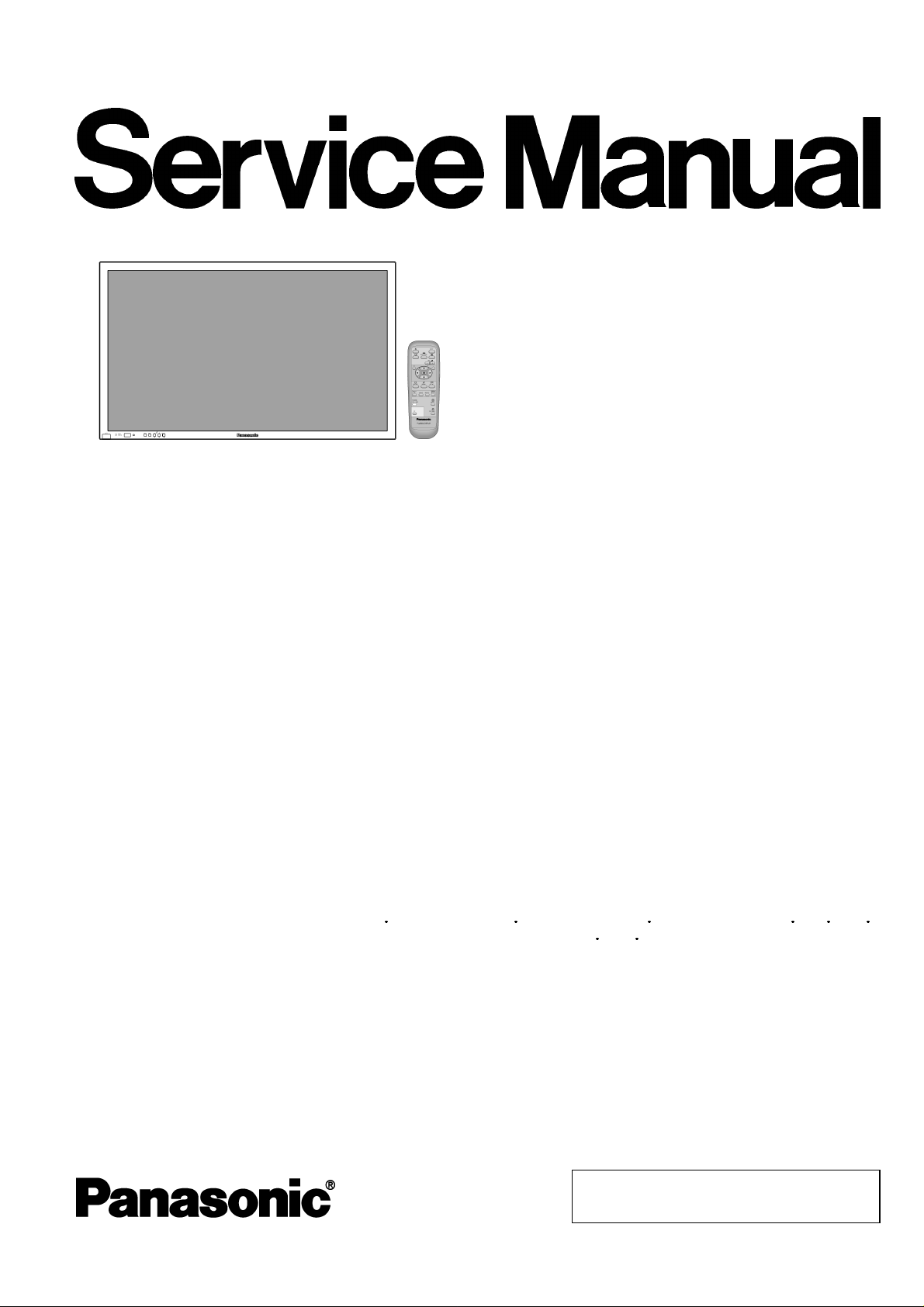
Panasonic TH-65PHD7UY, TH-65PHD7EK, TH-65PHD7BK Service manual
Order Number : ITD0410038C0
D10
High Definition Plasma Display
TH-65PHD7UY
TH-65PHD7EK
TH-65PHD7BK
GPH7D Chassis
Specifications
Power Source (UY Version) 120 V AC, 50 / 60 Hz
Power Source (Except UY) 220 - 240 V AC, 50 / 60 Hz
Power Consumption (UY Version)
Maximum 695W
Stand-by condition Save OFF1.0 W, Save ON 0.8 W
Power off condition 0.3 W
Power Consumption (Except UY)
Normal use 635 W
Stand-by condition Save off 1.0 W, Save on 0.8 W
Power off condition 0.3 W
Plasma Display panel Drive method: AC type 65-inch 16:9 aspect ratio
Contrast Ratio 3000:1
Screen size 1,434mm (W) × 806 mm (H) × 1,645 mm (diagonal)
(No. of pixels) 1,049,088 (1,366 (W) ×768 (H)) [4,098 × 768 dots]
Operating condition
Temperatuer 32 ° F - 104 ° F (0 ° C - 40 ° C)
Humidity 20 % - 80 %
Applicable signals
Colour System NTSC, PAL, PAL60, SECAM, Modified NTSC
Scanning format 525 (480) / 60i 60p, 625 (575) / 50i 50p, 750 (720) / 60p 50p, 1125 (1080) / 60i 50i 24p
25p 30p 24sF .... SMPTE274M, 1250 (1080) / 50i
PC signals XGAdisplay
VGA, SVGA, XGA
SXGA, UXGA ..... (compressed)
Horizontal scanning frequency 15 - 110 kHz
Vertical scanning frequency 48 - 120 Hz
Connection terminals
AV (UY Version) VIDEO IN
VIDEO OUT
S VIDEO IN (MINI DIN 4PIN) Y: 1 Vp-p (75-ohm), C: 0.286 Vp-p (75-ohm)
1.0 Vp-p (75-ohm or high impedance)
1.0 Vp-p (low impedance)
© 2004 Matsushita Electric Industrial Co., Ltd. All
rights reserved. Unauthorized copying and
distribution is a violation of law.

TH-65PHD7UY / TH-65PHD7EK / TH-65PHD7BK
AUDIO IN (RCA PIN JACK × 2) 0.5 Vrms (high impedance)
COMPONENT / RGB
(UY Version)
PC (UY Version) (HIGH-DENSITY D-SUB 15PIN) R, G, B / 0 .7 Vp-p (75-ohm)
PC (Except UY) (HIGH-DENSITY D-SUB 15PIN) R, G, B / 0.7 Vp-p (75-ohm)
SERIAL EXTERNAL CONTROL TERMINAL (D-SUB 9PIN) RS-232C COMPATIBLE
SPEAKERS (8 Ω ) 20 W [10 W + 10 W] (10 % THD)
Accessories Supplied
Remote Control Transmitter EUR646529
Batteries (UY Version) 2 × AA Size
Batteries (Except UY) 2 × R6 Size
Fixing bands (TMME203 or TMME187) × 2
Ferrite core J0KF00000018 × 1, J0KG00000054 × 2
Dimensions ( W × H × D ) 1,554 mm × 925 mm × 99 mm (without handles)
Mass (Weight) (UY Version)
main unit only approx. 179.7 lbs
with speakers approx. 189.4 lbs
Mass (Weight) (Except UY)
main unit only approx. 81.0 kg net
with speakers approx. 85.4 kg
Y / G (BNC) Y or G with / sync 1.0 Vp-p (75-ohm)
PB/ B (BNC), PR/ R (BNC) 0.7 Vp-p (75-ohm)
AUDIO IN (RCA PIN JACK × 2) 0.5 Vrms (high impedance)
PBPR/CBCR:0.7Vp-p (75-ohm)
AUDIO IN (M3 JACK) 0.5 Vrms (high impedance)
AUDIO IN (M3 JACK) 0.5 Vrms (high impedance)
G without / sync 0.7 Vp-p (75-ohm)
HD, VD / 1.0 - 5.0 Vp-p (high impedance)
Component
Y:1.0 Vp-p (75-ohm)
HD, VD / 1.0 - 5.0 Vp-p (high impedance)
HD, VD / 1.0 - 5.0 Vp-p (high impedance)
Notes:
· Design and specifications are subject to change without notice.Mass and dimensions shown are approximate.
CONTENTS
Page Page
1 Applicable signals 5
2 Safety Precautions
2.1. General Guidelines
3 Prevention of Electro Static Discharge (ESD) to
Electrostatically Sensitive (ES) Devices
4 About lead free solder (PbF)
5 PCB Structure sheet of GPH7D chassis
6 Service Hint
7 Disassembly/Exchange
7.1. Removal of the Back Cover
7.2. Exchange of the HA-Board(TH-65PHD7UY Only)
10
11
11
11
7.3. Exchange of the HB-Board(TH-65PHD7UY Only)
6
6
7
8
9
7.4. Removal of the Slot Block
7.5. Exchange of the J-Board
7.6. Exchange of the HX-Board
7.7. Exchange of the PF-Board
7.8. Exchange of the F-Board
7.9. Exchange of the Z-Board
7.10. Exchange of the D-Board
7.11. Exchange of the P-Board(SS-Boad side)
7.12. Exchange of the P-Board(SC-Board side)
7.13. Exchange of the PC-Board
11
11
12
12
12
13
13
14
14
15
15
2
TH-65PHD7UY / TH-65PHD7EK / TH-65PHD7BK
7.14. Exchange of the SU-Board and the SD-Board 16
7.15. Exchange of the SC-Board
7.16. Exchange of the SS2-Board and the SS3-Board
7.17. Exchange of the SS-Board
7.18. Exchange of the C1, C2, C3-Board
7.19. Exchange of the C4, C5, C6-Board
7.20. Exchange of the Fan
7.21. Exchange of the Escutcheon
7.22. Exchange of the Plasma Panel
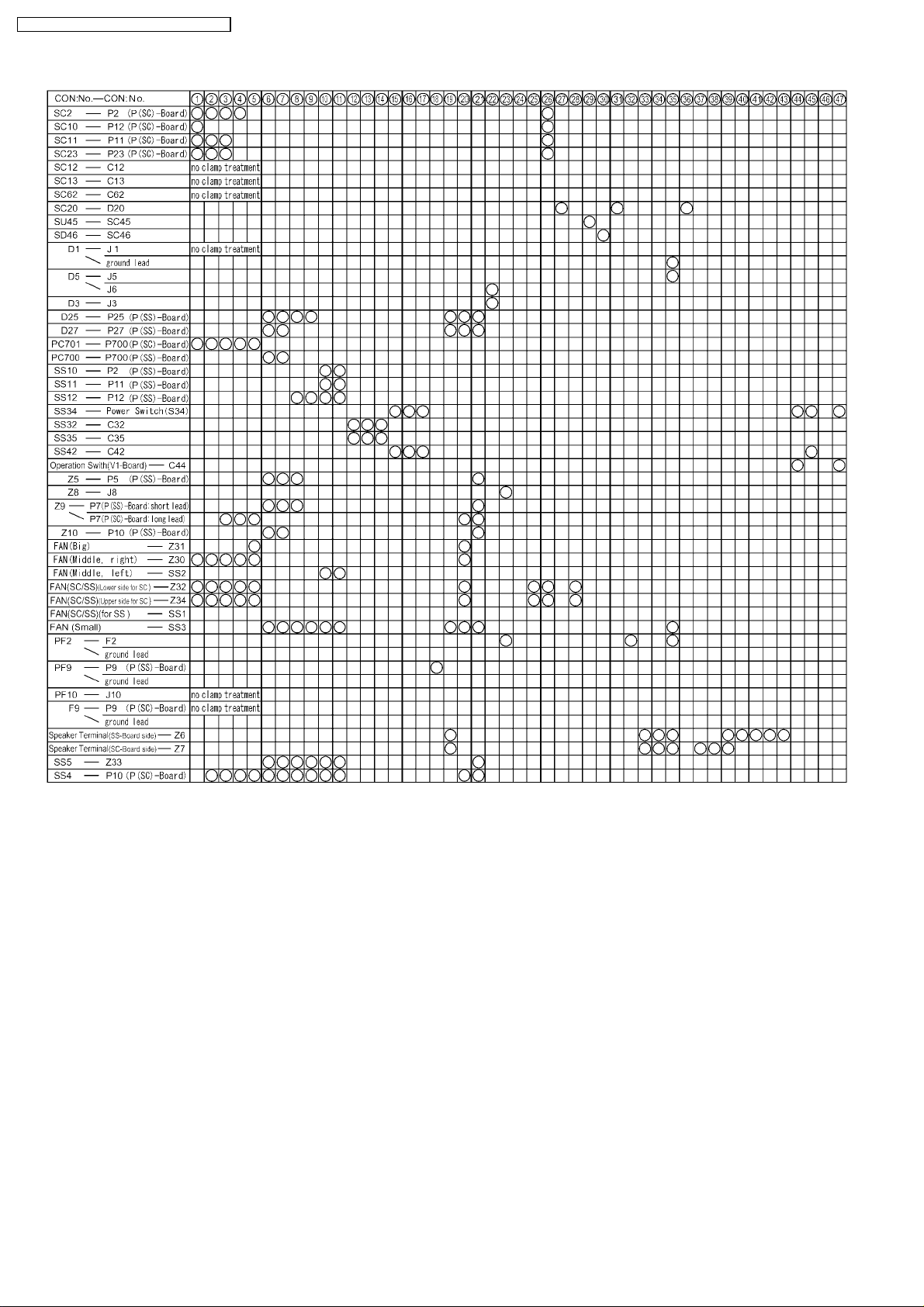
8 Location of Lead Wiring
9 Adjustment Procedure
9.1. Driver Set-up
9.2. Initialization Pulse Adjust
9.3. P.C.B. (Printed Circuit Board) exchange
9.4. Adjustment Volume Location
9.5. Test Point Location
10 Service mode
10.1. CAT (computer Aided Test) mode
10.2. IIC mode structure (following items value is sample data.)
11 Alignment
11.1. PC / RGB / NTSC / PAL / DVI panel white balance
11.2. HD / 525i / 525p / 625i / 625p panel white balance
12 Trouble shooting guide
12.1. Self Check
12.2. No Power
12.3. No Picture
12.4. Local screen failure
13 Option Setting
13.1. How to access and setting
13.2. Contents of Option Menu
14 Circuit Board Layout
14.1. PF-Board
14.2. PC-Board
14.3. P(SS)-Board
14.4. P(SC)-Board
14.5. F-Board
14.6. HA-Board(TH-65PHD7UY only)
14.7. HB-Board(TH-65PHD7UY only)
14.8. HX-Board
14.9. J-Board
14.10. D-Board
14.11. C1-Board
14.12. C2-Board
14.13. C3-Board
14.14. C4-Board
14.15. C5-Board
14.16. C6-Board
14.17. SC-Board
14.18. SU-Board
14.19. SD-Board
14.20. SS-Board
14.21. SS2 and SS3-Board
14.22. Z-Board
14.23. H3, S1 and V1-Board
15 Schematic Diagrams
16
17
17
18
18
19
20
21
27
29
29
30
31
31
31
32
32
15.1. Schematic Diagram Notes
15.2. Main Block Diagram
15.3. PF and F-Board Block Diagram
15.4. PF and F-Board Schematic Diagram
15.5. PC-Board Block Diagram
15.6. PC-Board Schematic Diagram
15.7. P(SS)-Board Block Diagram
15.8. P(SC)-Board Block Diagram
15.9. P(SS)-Board (1 of 6) Schematic Diagram
15.10. P(SS)-Board (2 of 6) Schematic Diagram
15.11. P(SS)-Board (3 of 6) Schematic Diagram
15.12. P(SS)-Board (4 of 6) Schematic Diagram
15.13. P(SS)-Board (5 of 6) Schematic Diagram
15.14. P(SS)-Board (6 of 6) Schematic Diagram
15.15. P(SC)-Board (1 of 6) Schematic Diagram
15.16. P(SC)-Board (2 of 6) Schematic Diagram
15.17. P(SC)-Board (3 of 6) Schematic Diagram
34
35
35
38
40
40
15.18. P(SC)-Board (4 of 6) Schematic Diagram
15.19. P(SC)-Board (5 of 6) Schematic Diagram
15.20. P(SC)-Board (6 of 6) Schematic Diagram
15.21. HA, HB and HX-Board Block Diagram
15.22. HA-Board Schematic Diagram (TH-65PHD7UY only)
15.23. HB-Board (1 of 2) Schematic Diagram (TH-65PHD7UY
41
42
15.24. HB-Board (2 of 2) Schematic Diagram(TH-65PHD7UY
42
43
43
44
45
45
46
47
50
53
54
55
56
57
58
60
61
62
63
64
65
66
15.25. HX-Board Schematic Diagram
15.26. J-Board Block Diagram
15.27. J-Board (1 of 4) Schematic Diagram
15.28. J-Board (2 of 4) Schematic Diagram
15.29. J-Board (3 of 4) Schematic Diagram
15.30. J-Board (4 of 4) Schematic Diagram
15.31. D-Board Block Diagram
15.32. D-Board (1 of 12) Schematic Diagram
15.33. D-Board (2 of 12) Schematic Diagram
15.34. D-Board (3 of 12) Schematic Diagram
15.35. D-Board (4 of 12) Schematic Diagram
15.36. D-Board (5 of 12) Schematic Diagram
15.37. D-Board (6 of 12) Schematic Diagram
15.38. D-Board (7 of 12) Schematic Diagram
15.39. D-Board (8 of 12) Schematic Diagram
15.40. D-Board (9 of 12) Schematic Diagram
15.41. D-Board (10 of 12) Schematic Diagram
15.42. D-Board (11 of 12) Schematic Diagram
15.43. D-Board (12 of 12) Schematic Diagram
15.44. C1, C2, C5 and C6-Board Block Diagram
15.45. C3, C4, SS, SS2, SS3 S1 and V1-Board Block Diagram
69
70
71
74
75
15.46. C1-Board (1 of 2) Schematic Diagram
15.47. C1-Board (2 of 2) Schematic Diagram
15.48. C2-Board (1 of 3) Schematic Diagram
15.49. C2-Board (2 of 3) Schematic Diagram
only)
only)
77
79
79
80
81
82
83
84
85
86
87
88
89
90
91
92
93
94
95
96
97
98
99
100
101
102
103
104
105
106
107
108
109
110
111
112
113
114
115
116
117
118
119
120
121
122
123
124
125
126
127
3
TH-65PHD7UY / TH-65PHD7EK / TH-65PHD7BK
15.50. C2-Board (3 of 3) Schematic Diagram 128
15.51. C3-Board (1 of 2) Schematic Diagram
15.52. C3-Board (2 of 2) Schematic Diagram
15.53. C4-Board (1 of 2) and V1 Schematic Diagram
15.54. C4-Board (2 of 2) Schematic Diagram
15.55. C5-Board (1 of 3) Schematic Diagram
15.56. C5-Board (2 of 3) Schematic Diagram
15.57. C5-Board (3 of 3) Schematic Diagram
15.58. C6-Board (1 of 2) Schematic Diagram
15.59. C6-Board (2 of 2) Schematic Diagram
15.60. SS-Board (1 of 2) and S1 Schematic Diagram
15.61. SS-Board (2 of 2) ,SS2 and SS3 Schematic Diagram
15.62. SC, SU and SD-Board Block Diagram
15.63. SC-Board (1 of 4) Schematic Diagram
15.64. SC-Board (2 of 4) Schematic Diagram
15.65. SC-Board (3 of 4) Schematic Diagram
15.66. SC-Board (4 of 4) Schematic Diagram
129
130
131
132
133
134
135
136
137
138
139
140
141
142
143
144
15.67. SU-Board (1 of 2) Schematic Diagram
15.68. SU-Board (2 of 2) Schematic Diagram
15.69. SD-Board (1 of 2) Schematic Diagram
15.70. SD-Board (2 of 2) Schematic Diagram
15.71. Z and H3-Board Block Diagram
15.72. Z-Board (1 of 2) and H3 Schematic Diagram
15.73. Z-Board (2 of 2) Schematic Diagram
16 Parts Location
16.1. Exploded View
16.2. Fan and cover location
16.3. Cable relation
16.4. Packing summary
17 Mechanica l Replacement Parts List
18 Replacement Parts List
18.1. Replacement Parts List Notes
18.2. Electrical Replacement Parts List TH-65PHD7UY/EK/BK
145
146
147
148
149
150
151
153
153
155
155
156
160
162
162
163
4
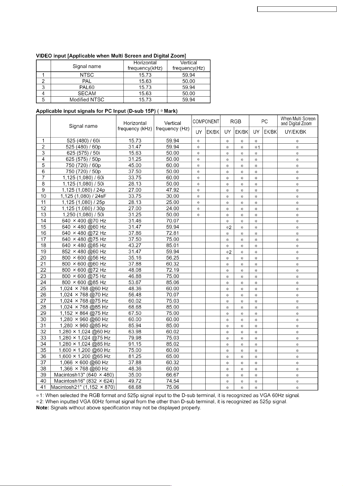
1 Applicable signals
TH-65PHD7UY / TH-65PHD7EK / TH-65PHD7BK
5
TH-65PHD7UY / TH-65PHD7EK / TH-65PHD7BK
2 Safety Precautions
2.1. General Guidelines
1. When servicing, observe the original lead dress. If a short circuit is found, replace all parts which have been overheated or
damaged by the short circuit.
2. After servicing, see to it that all the protective devices such as insulation barriers, insulation papers shields are properly
installed.
3. After servicing, make the following leakage current checks to prevent the customer from being exposed to shock hazards.
2.1.1. Leakage Current Cold Check
1. Unplug the AC cord and connect a jumper between the two
prongs on the plug.
2. Measure the resistance value, with an ohmmeter, between
the jumpered AC plug and each exposed metallic cabinet
part on the equipment such as screwheads, connectors,
control shafts, etc. When the exposed metallic part has a
return path to thechassis, the reading should be between
1MΩ and 5.2MΩ.
When the exposed metal does not have a return path to
the chassis, the reading must be
.
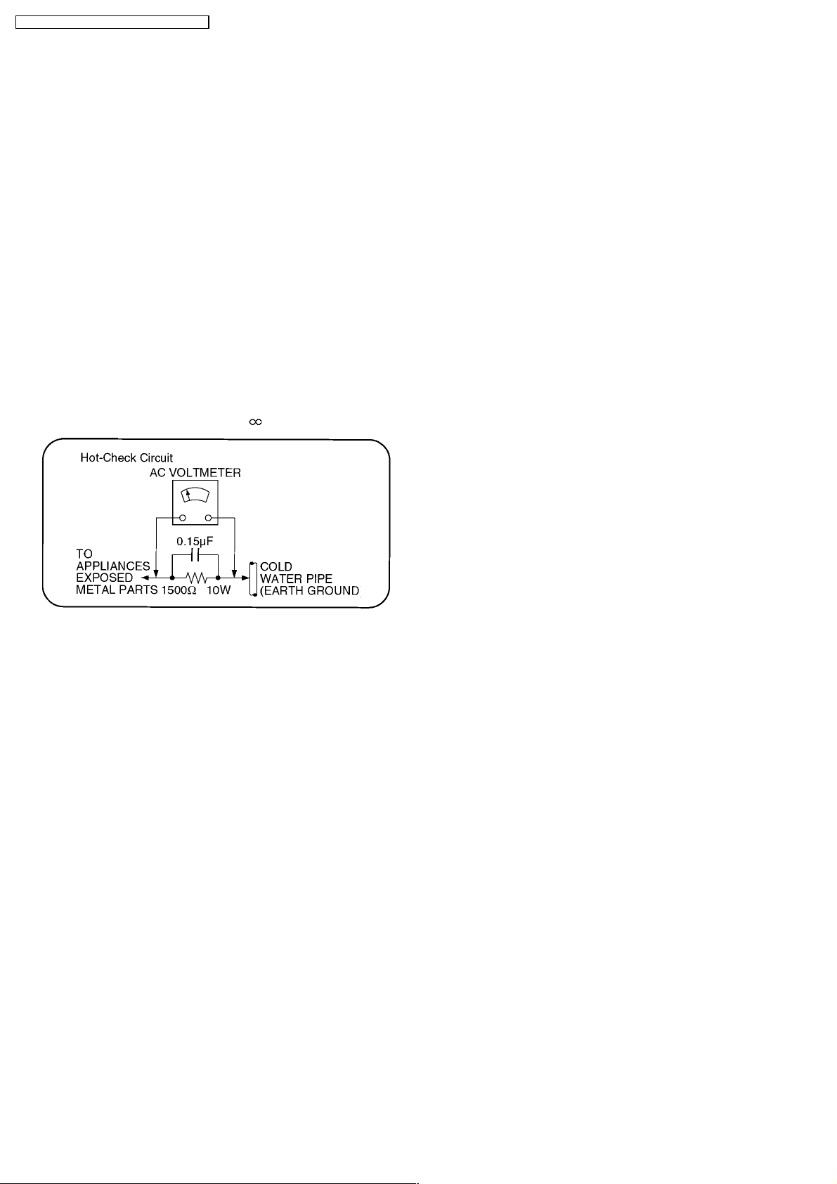
Figure 1
2.1.2. Leakage Current Hot Check (See
Figure 1.)
1. Plug the AC cord directly into the AC outlet. Do not use an
isolation transformer for this check.
2. Connect a 1.5kΩ, 10 watts resistor, in parallel with a 0.15µF
capacitors, between each exposed metallic part on the set
and a good earth ground such as a water pipe, as shown in
Figure 1.
3. Use an AC voltmeter, with 1000 ohms/volt or more
sensitivity, to measure the potential across the resistor.
4. Check each exposed metallic part, and measure the
voltage at each point.
5. Reverse the AC plug in the AC outlet and repeat each of the
above measurements.
6. The potential at any point should not exceed 0.75 volts
RMS. A leakage current tester (Simpson Model 229 or
equivalent) may be used to make the hot checks, leakage
current must not exceed 1/2 milliamp. In case a
measurement is outside of the limits specified, there is a
possibility of a shock hazard, and the equipment should be
repaired and rechecked before it is returned to the
customer.
6
TH-65PHD7UY / TH-65PHD7EK / TH-65PHD7BK
3 Prevention of Electro Static Discharge (ESD) to
Electrostatically Sensitive (ES) Devices
Some semiconductor (solid state) devices can be damaged easily by static electricity. Such components commonly are called
Electrostatically Sensitive (ES) Devices. Examples of typical ES devices are integrated circuits and some field-effect transistorsand
semiconductor "chip" components. The following techniques should be used to help reduce the incidence of component damage
caused by electro static discharge (ESD).
1. Immediately before handling any semiconductor component or semiconductor-equipped assembly, drain off any ESD on your
body by touching a known earth ground. Alternatively, obtain and wear a commercially available discharging ESD wrist strap,
whichshould be removed for potential shock reasons prior to applying power to the unit under test.
2. After removing an electrical assembly equipped with ES devices, place the assembly on a conductive surface such as alminum
foil, to prevent electrostatic charge buildup or exposure of the assembly.
3. Use only a grounded-tip soldering iron to solder or unsolder ES devices.
4. Use only an anti-static solder removal device. Some solder removal devices not classified as "anti-static (ESD protected)" can
generate electrical charge sufficient to damage ES devices.
5. Do not use freon-propelled chemicals. These can generate electrical charges sufficient to damage ES devices.
6. Do not remove a replacement ES device from its protective package until immediately before you are ready to install it. (Most
replacement ES devices are packaged with leads electrically shorted together by conductive foam, alminum foil or
comparableconductive material).
7. Immediately before removing the protective material from the leads of a replacement ES device, touch the protective material
to the chassis or circuit assembly into which the device will be installed.
Caution
Be sure no power is applied to the chassis or circuit, and observe all other safety precautions.
8. Minimize bodily motions when handling unpackaged replacement ES devices. (Otherwise hamless motion such as the brushing
together of your clothes fabric or the lifting of your foot from a carpeted floor can generate static electricity (ESD) sufficient
todamage an ES device).
7

TH-65PHD7UY / TH-65PHD7EK / TH-65PHD7BK
4 About lead free solder (PbF)
Note: Lead is listed as (Pb) in the periodic table of elements.
In the information below, Pb will refer to Lead solder, and PbF will refer to Lead Free Solder.
The Lead Free Solder used in our manufacturing process and discussed below is (Sn+Ag+Cu).
That is Tin (Sn), Silver (Ag) and Copper (Cu) although other types are available.
This model uses Pb Free solder in it’s manufacture due to environmental conservation issues. For service and repair work, we’d
suggest the use of Pb free solder as well, although Pb solder may be used.
PCBs manufactured using lead free solder will have the PbF within a leaf Symbol
Caution
· Pb free solder has a higher melting point than standard solder. Typically the melting point is 50 ~ 70 °F (30~40 °C) higher.
Please use a high temperature soldering iron and set it to 700 ± 20 °F (370 ± 10 °C).
· Pb free solder will tend to splash when heated too high (about 1100 °F or 600 °C).
If you must use Pb solder, please completely remove all of the Pb free solder on the pins or solder area before applying Pb
solder. If this is not practical, be sure to heat the Pb free solder until it melts, before applying Pb solder.
· After applying PbF solder to double layered boards, please check the component side for excess solder which may flow onto
the opposite side. (see figure below)
Suggested Pb free solder
There are several kinds of Pb free solder available for purchase. This product uses Sn+Ag+Cu (tin, silver, copper) solder.
However, Sn+Cu (tin, copper), Sn+Zn+Bi (tin, zinc, bismuth) solder can also beused.
stamped on the back of PCB.
8
5 PCB Structure sheet of GPH7D chassis
Board Name Function Remarks
D Digital Signal Processor 1
F Power filter 1
J Slot Interface & SYNC processor 1
Z Audio out, DC-DC converter
SS Sustain out 1
SC Scan out 1
SU Scan connection (Upper) 1
SD Scan connection (Lower) 1
C1 Data Drive (Upper Right)
C2 Data Drive (Upper Center)
C3 Data Drive (Upper Left)
C4 Data Drive (Lower Left)
C5 Data Drive (Lower Center)
C6 Data Drive (Lower Right)
H3 Speaker terminal
S1 Power switch
SS2 Sustain connection (Upper)
SS3 Sustain connection (Lower)
V1 Front SW. & Remote receiver
PC Power control 1
PF Line filter 1
P(SC) Power supply 1
P(SS) Power supply 1
HX PC_type_Input terminal
HB BNC Composite/Component Video 2
HA BNC Component Video 2
TH-65PHD7UY / TH-65PHD7EK / TH-65PHD7BK
Remarks
1. Recommend PCB´s for initial service for GPH7D chassis.
2. For System model except BKJ, EKJ model.
9
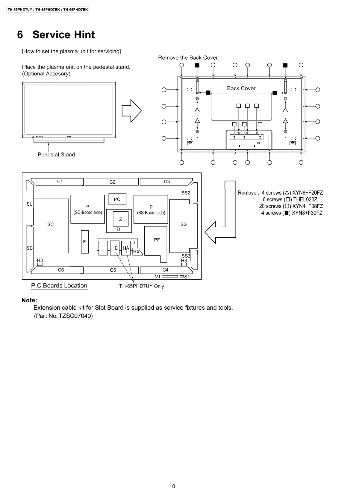
7 Disassembly/Exchange
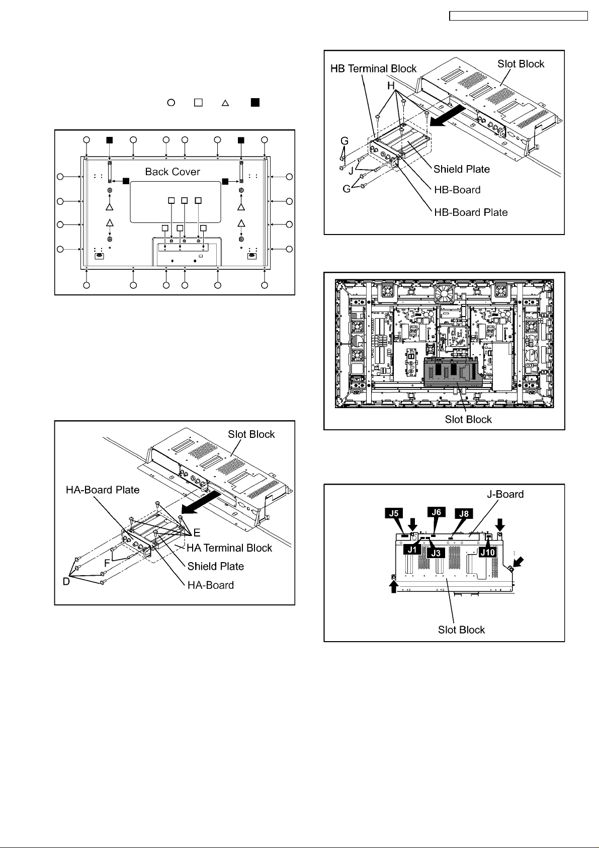
7.1. Removal of the Back Cover
1. Remove the screws (×20 ,×6 ,×4 ,×4 ) and then
remove the Back Cover.
TH-65PHD7UY / TH-65PHD7EK / TH-65PHD7BK
7.4. Removal of the Slot Block
7.2. Exchange of the HA-Board
(TH-65PHD7UY Only)
1. Remove the 4 screws(D) of the HA Terminal Block and then
remove the HA Terminal Block.
2. Remove the 4 screws(E) of the Shield Plate.
3. Remove the 2 screws(F) of the HA-Board Plate and then
exchange the HA-Board.
1. Disconnect the couplers (J1, J3, J5, J6, J8, J10).
2. Remove the 4 screws of the Slot Block andthen remove the
Slot Block.
7.3. Exchange of the HB-Board
(TH-65PHD7UY Only)
1. Remove the 4 screws(G) of the HB Terminal Block and then
remove the HB Terminal Block.
2. Remove the 4 screws(H) of the Shield Plate.
3. Remove the 2 screws(J) of the HB-Board Plate and then
exchange the HB-Board.
11
TH-65PHD7UY / TH-65PHD7EK / TH-65PHD7BK
7.5. Exchange of the J-Board
1. Remove the HA Terminal Block and the HB Terminal Block.
(Reference to Exchange of the HA-Board and Exchange of
the HB-Board)
2. Remove the Slot Block.
(Reference to Removal of the Slot Block)
3. Remove the 7 screws of the J-Board and then remove the
J-Board.
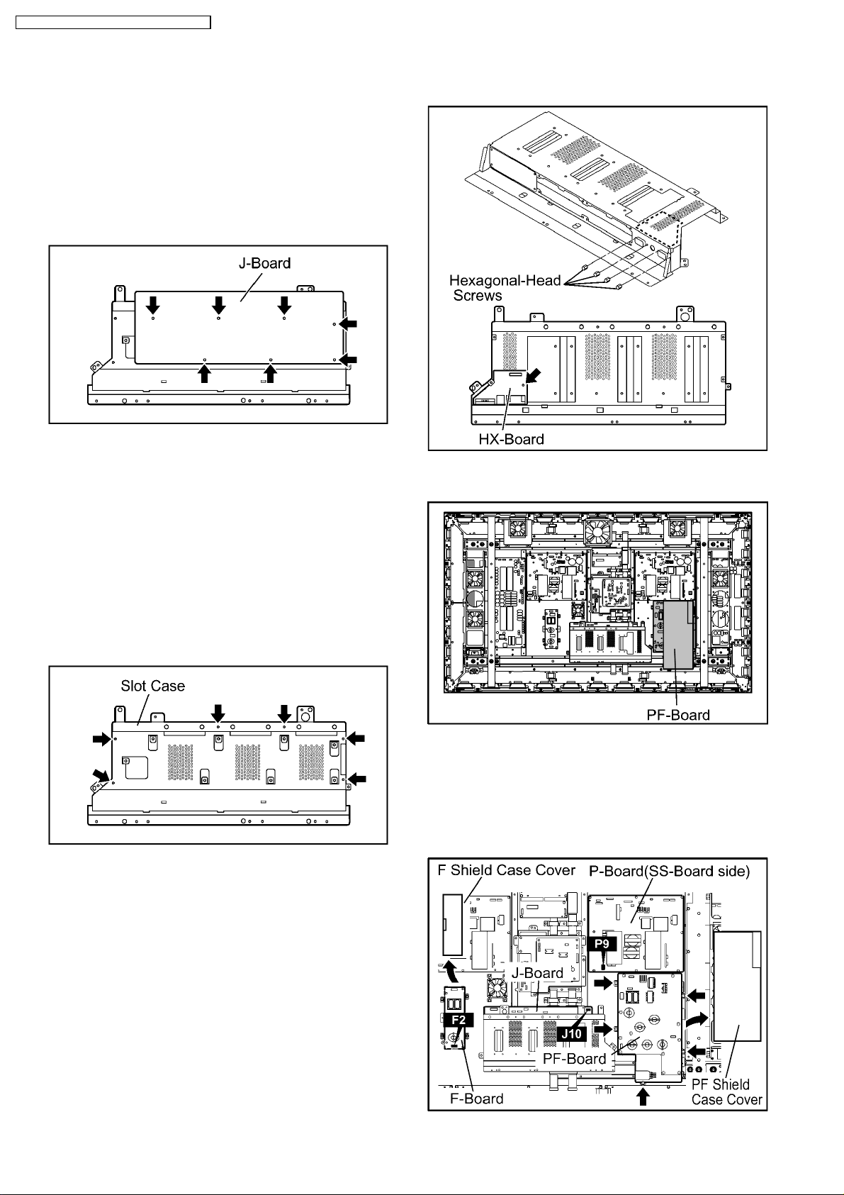
7.6. Exchange of the HX-Board
1. Remove the HA Terminal Block and the HB Terminal Block.
(Reference to Exchange of the HA-Board and Exchange of
the HB-Board)
2. Remove the Slot Block.
(Reference to Removal of the Slot Block)
3. Remove the J-Board.
(Reference to Exchange of the J-Board)
4. Remove the 6 screws of the Slot Case and then remove the
Slot Case.
5. Remove the 4 Hexagonal-Head screws and the screw of
the HX-Board and then exchange the HX-Board.
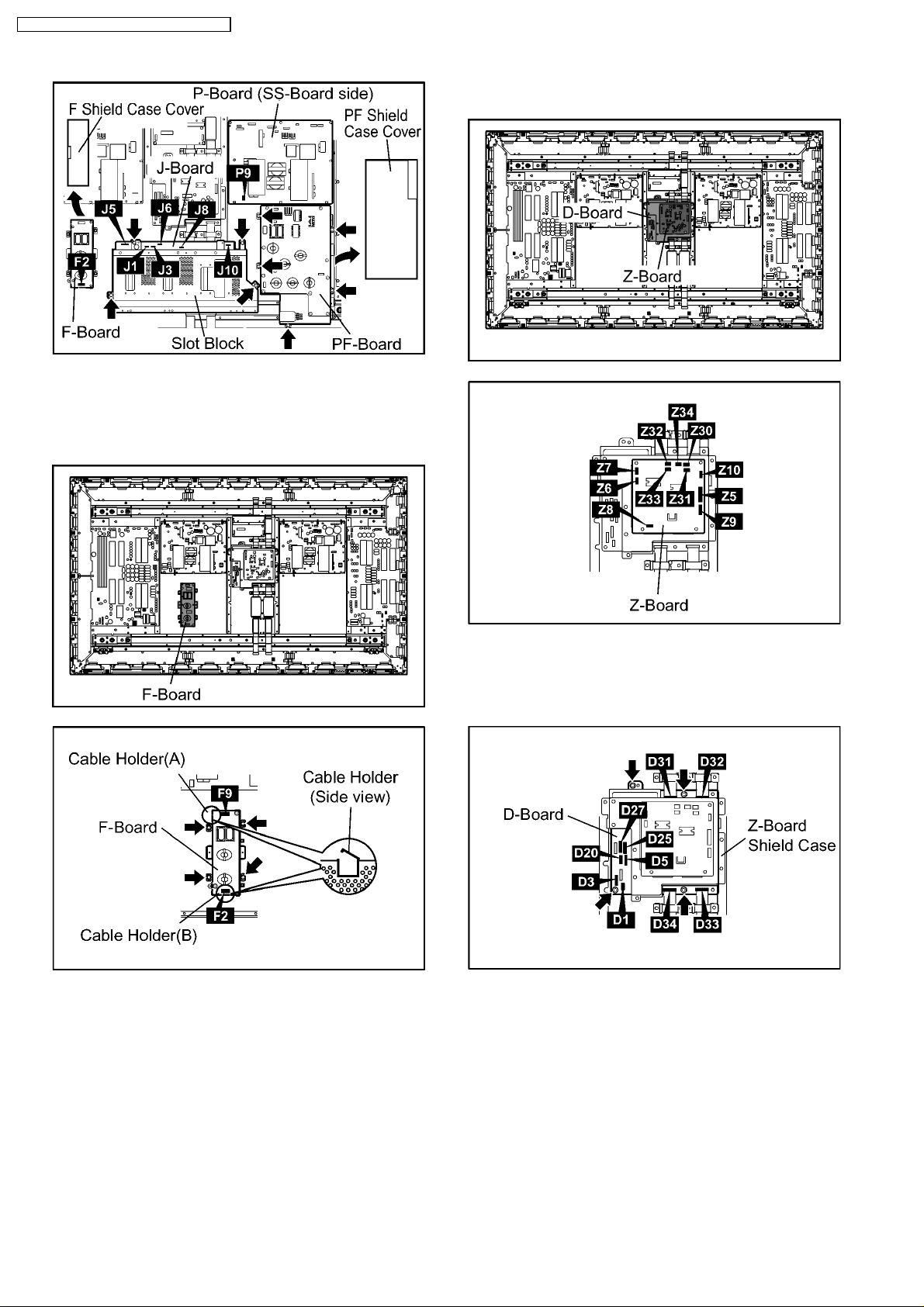
7.7. Exchange of the PF-Board
1. Remove the PF Shield Case Cover.
2. Disconnect the couplers(J10, P9)
3. Remove the F Shield Case Cover and then disconnect the
coupler(F2).
4. Remove the 5 screws of the PF-Board and then exchange
the PF-Board.
12
TH-65PHD7UY / TH-65PHD7EK / TH-65PHD7BK
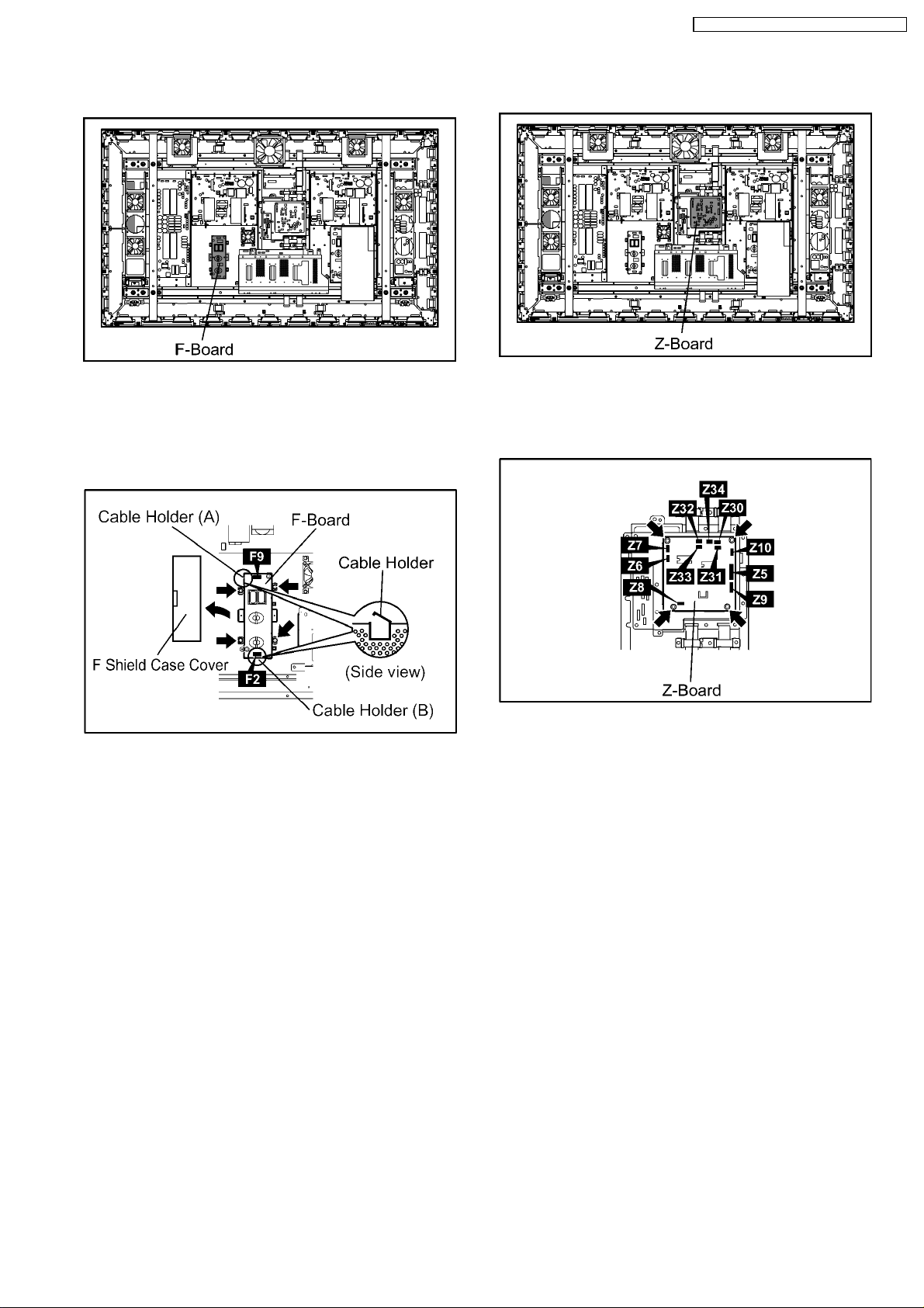
7.8. Exchange of the F-Board
1. Remove the F Shield Case Cover.
2. Disconnect the couplers(F2, F9).
3. Release 2 sets of cables from the Cable Holders(A, B).
4. Remove the 4 screws of the F-Board and then exchange
the F-Board.
7.9. Exchange of the Z-Board
1. Disconnect the couplers(Z5, Z6, Z7, Z8, Z9, Z10, Z30, Z31,
Z32, Z33, Z34).
2. Remove the 4 screws of the Z-Board and then exchange
the Z-Board.
13

TH-65PHD7UY / TH-65PHD7EK / TH-65PHD7BK
7.10. Exchange of the D-Board
1. Remove the Z-Board.
(Reference to Exchange of the Z-Board)
2. Remove the 4 screws of Z-Board Shield Case and then
remove the Z-Board Shield Case.
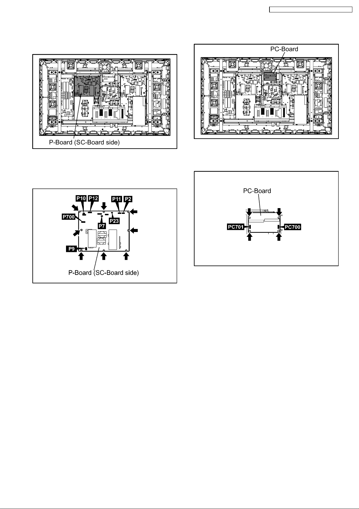
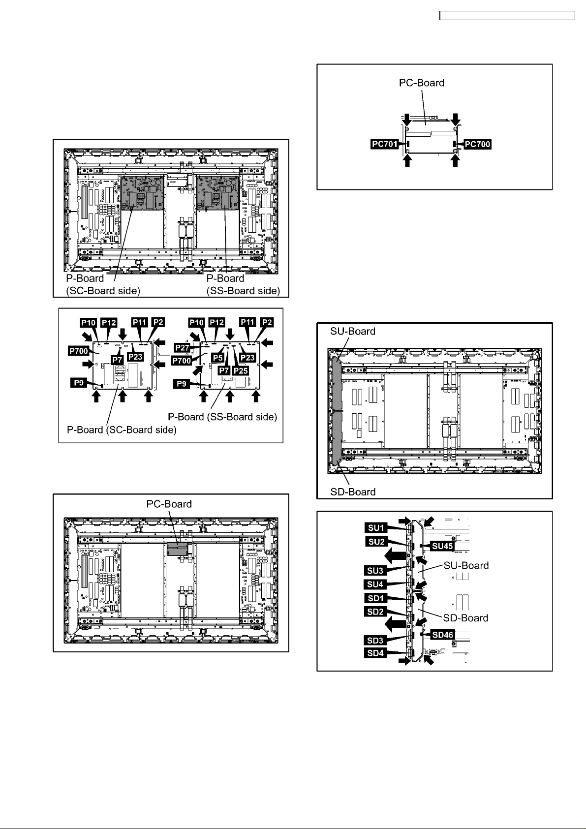
7.11. Exchange of the P-Board(SSBoad side)
1. Disconnect the couplers(P2, P5, P7, P9, P10, P11, P12,
P25, P27, P700).
2. Remove the 8 screws of the P-Board(SS-Board side) and
then exchange the P-Board(SS-Board side).
3. Disconnect the couplers(D1, D3, D5, D20, D25, D27, D31,
D32, D33, D34).
4. Remove the 4 screws of the D-Board and then exchange
the D-Board.
Caution:
At the time of exchange of the P-Board(SS-Board side)
disconnect the dummy couplers(P25, P27) and then
connect the couplers.
14
TH-65PHD7UY / TH-65PHD7EK / TH-65PHD7BK
7.12. Exchange of the P-Board(SCBoard side)
1. Disconnect the couplers(P2, P7, P9, P10, P11, P12, P23,
P700).
2. Remove the 8 screws of the P-Board(SC-Board side) and
then exchange the P-Board(SC-Board side).
7.13. Exchange of the PC-Board
1. Disconnect the couplers(PC700, PC701).
2. Remove the 4 screws of the PC-Board and then exchange
the PC-Board.
Caution:
At the time of exchange of the P-Board(SC-Board side)
does not disconnect the dummy couplers(P25, P27).
15
TH-65PHD7UY / TH-65PHD7EK / TH-65PHD7BK
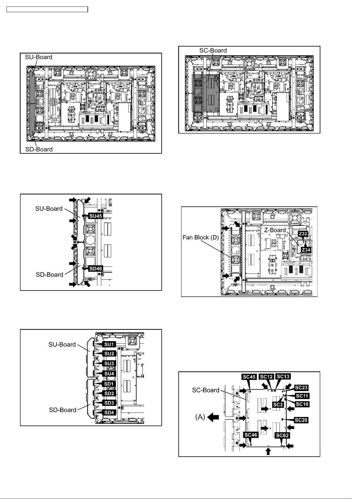
7.14. Exchange of the SU-Board and
the SD-Board
1. Remove the each 4 screws of the SU-Board and the SD-
Board.
2. Slide the SU-Board and the SD-Board to the left.
3. Disconnect the couplers(SU45, SD46).
7.15. Exchange of the SC-Board
1. Remove the each 4 screws of the SU-Board and the SDBoard.
2. Slide the SU-Board and the SD-Board to the left.
(Reference to Exchange of the SU-Board and the SD-
Board)
3. Disconnect the couplers(Z32, Z34).
4. Remove the 4 screws of the Fan Block(D) and then remove
the Fan Block(D).
4. Disconnect the couplers(SU1, SU2, SU3, SU4) and then
exchange the SU-Board.
5. Disconnect the couplers(SD1, SD2, SD3, SD4) and then
exchange the SD-Board.
5. Disconnect the couplers(SC2, SC10, SC11, SC12, SC13,
SC20, SC23, SC45, SC46, SC62).
6. Remove the 11 screws ofthe SC-Board, slide theSC-Board
in the direction of the arrow(A) and then exchange the SCBoard.
Caution:.
Don’t damage the flexible cables(SU, SD) and the parts
on the SC-Board.
16
TH-65PHD7UY / TH-65PHD7EK / TH-65PHD7BK
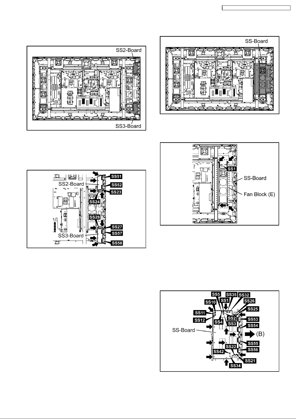
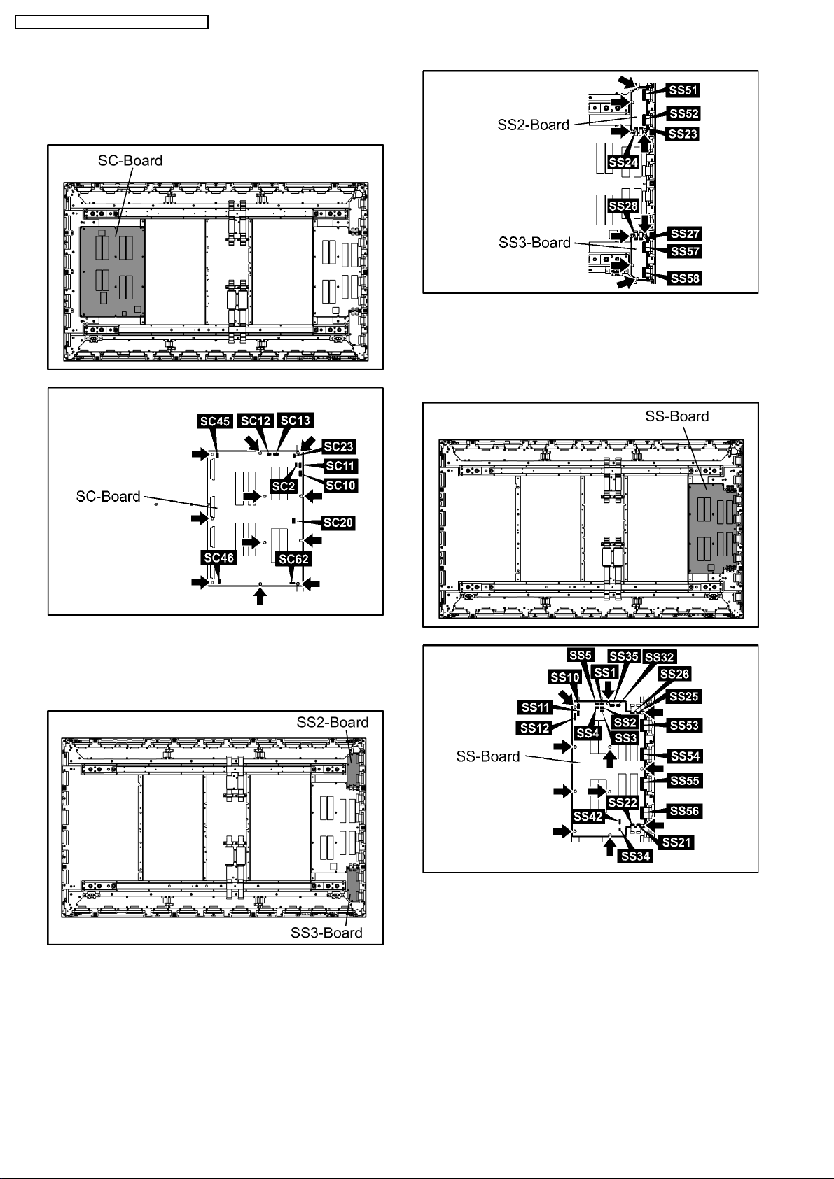
7.16. Exchange of the SS2-Board
and the SS3-Board
1. Disconnect the couplers(SS23, SS24, SS51, SS52).
2. Disconnect the couplers(SS27, SS28, SS57, SS58).
3. Remove the each 4 screws of the SS2-Board and the SS3-
Board and then exchange the SS2-Board and the SS3Board.
7.17. Exchange of the SS-Board
1. Disconnect the coupler(SS1).
2. Remove the 4 screws of the Fan Block(E) and then remove
the Fan Block(E).
3. Disconnect the couplers(SS1, SS2, SS3, SS4, SS5, SS10,
SS11, SS12, SS21, SS22, SS25, SS26, SS32, SS34,
SS35, SS42, SS53, SS54, SS55, SS56).
4. Remove the 11 screws of the SS-Board, slide the SS-Board
in the direction of the arrow(B) and then exchange the SSBoard.
Caution:
Don’t damage the flexible cables of the Plasma Display
and the parts on the SS-Board.
17
TH-65PHD7UY / TH-65PHD7EK / TH-65PHD7BK
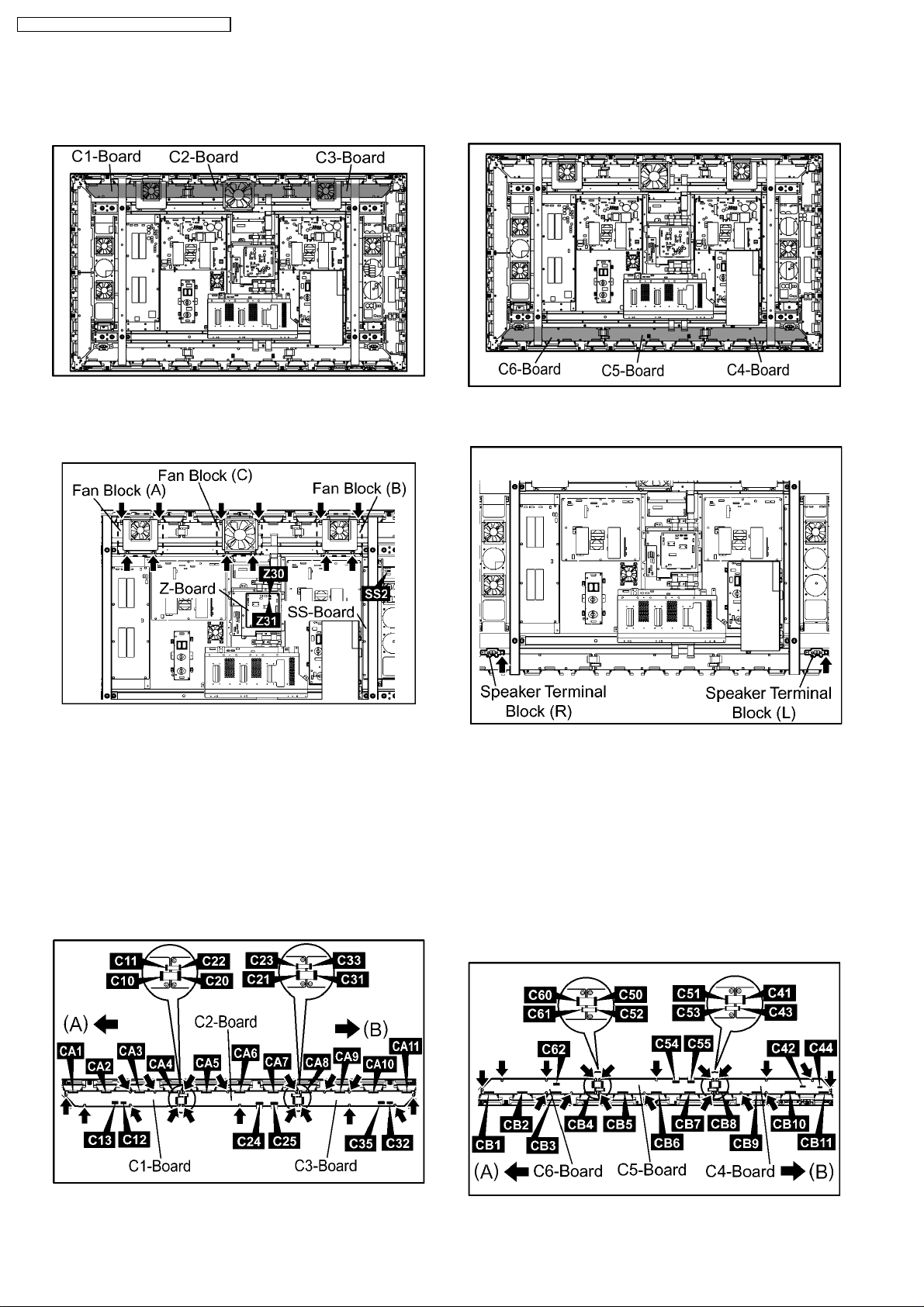
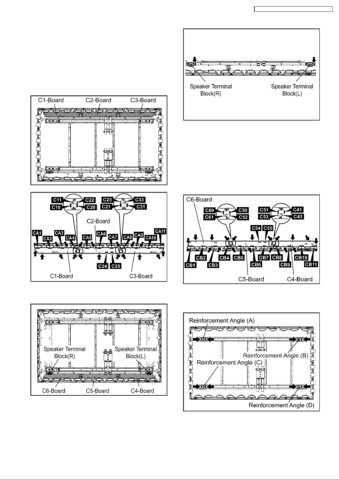
7.18. Exchange of the C1, C2, C3Board
1. Disconnect the couplers(Z30, Z31, SS2).
2. Remove the each 4 screws of the Fan Blocks(A, B, C) and
then remove the Fan Blocks(A, B, C).
7.19. Exchange of the C4, C5, C6Board
1. Remove the each screw of the Speaker Terminal Blocks(L,
R) and then remove the Speaker Terminal Blocks(L, R).
3. Disconnect the couplers(C10, C11, C12, C13, CA1, CA2,
CA3, CA4) on the C1-Board.
4. Disconnect the couplers(C20, C21, C22, C23, C24, C25,
CA5, CA6, CA7) on the C2-Board.
5. Disconnect the couplers(C31, C32, C33, C35, CA8, CA9,
CA10, CA11) on the C3-Board.
6. Remove the each 6 screws of the C1-Board, the C2-Board
and the C3-Board, slide the C1-Board in the direction of the
arrow(A), the C3-Board in the direction of the arrow(B) and
then exchange the C1-Board, the C2-Board and the C3Board.
2. Disconnect the couplers(C41, C42, C43, C44, CB8, CB9,
CB10, CB11) on the C4-Board.
3. Disconnect the couplers(C50, C51, C52, C53, C54, C55,
CB5, CB6, CB7) on the C5-Board.
4. Disconnect the couplers(C60, C61, C62, CB1, CB2, CB3,
CB4) on the C6-Board.
5. Remove the each 6 screws of the C4-Board, the C5-Board
and the C6-Board, slide the C4-Board in the direction of the
arrow(B), the C6-Board in the direction of the arrow(A) and
then exchange the C4-Board, the C5-Board and the C6Board.
18
TH-65PHD7UY / TH-65PHD7EK / TH-65PHD7BK
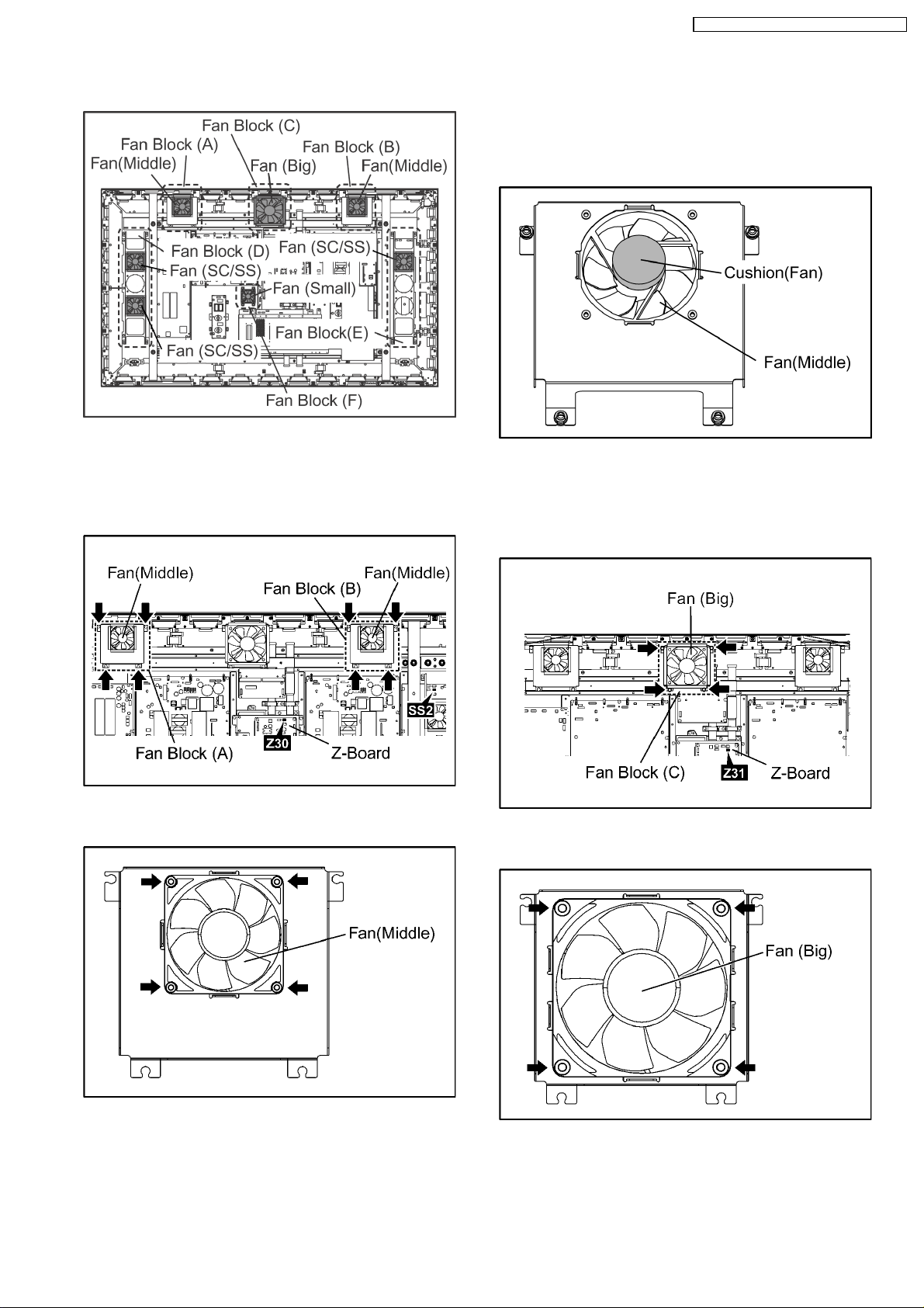
7.20. Exchange of the Fan
7.20.1. Exchange of the Fan(Middle)
1. Disconnect the couplers(Z30, SS2).
2. Remove the each 4 screws of the Fan Blocks(A, B) and
then remove the Fan Blocks(A, B).
4. Reassemble the Fans in reverse order (3-1) and then stick
the Cushion (Fan) on the central part of the Fan.
Note:
The Cushion (Fan) is unsuitable to reuse.
Please use a new one at the time of Fan exchange.
7.20.2. Exchange of the Fan(Big)
1. Disconnect the coupler(Z31).
2. Remove the 4 screws of the Fan Block(C) and then remove
the Fan Block(C).
3. Remove the each 4 screws of the 2 Fans(Middle) and then
exchange the 2 Fans(Middle).
3. Remove the 4 screws of the Fan(Big) and then exchange
the Fan(Big).
19
TH-65PHD7UY / TH-65PHD7EK / TH-65PHD7BK
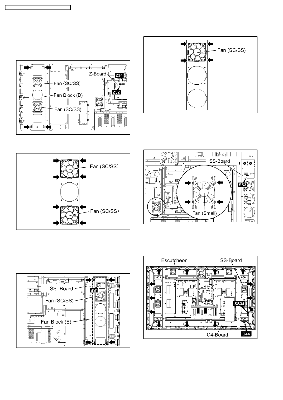
7.20.3. Exchange of the Fan(SC/SS) on
the SC-Board side
1. Disconnect the couplers(Z32, Z34).
2. Remove the 4 screws of the Fan Block(D) and then remove
the Fan Block(D).
3. Remove the each 4 screws of the 2 Fans(SC/SS) and then
exchange the 2 Fans(SC/SS).
3. Remove the 4 screws of the Fan(SC/SS) and then
exchange the Fan(SC/SS).
7.20.5. Exchange of the Fan(Small)
1. Disconnect the coupler(SS3).
2. Remove the 4 screws of the Fan(Small) and then exchange
the Fan(Small).
7.20.4. Exchange of the Fan(SC/SS) on
the SS-Board side
1. Disconnect the coupler(SS1).
2. Remove the 4 screws of the Fan Block(E) and then remove
the Fan Block(E).
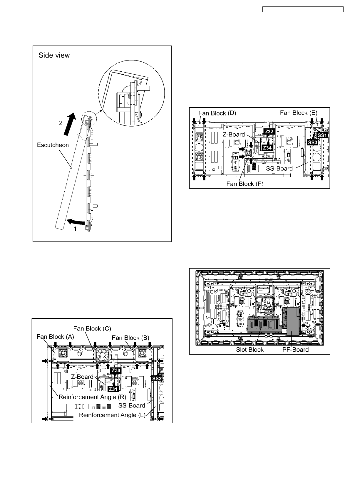
7.21. Exchange of the Escutcheon
1. Remove the 13 screws of the Escutcheon.
2. Disconnect the couplers(C44, SS34).
20
TH-65PHD7UY / TH-65PHD7EK / TH-65PHD7BK
3. Pull the bottom of the Escutcheon forward. (arrow1)
4. Lift up the Escutcheon to remove.(arrow2)
4. Disconnect the couplers(Z32, Z34).
5. Remove the 4 screws of the Fan Block(D) and then remove
the Fan Block(D).
6. Disconnect the coupler(SS1).
7. Remove the 4 screws of the Fan Block(E) and then remove
the Fan Block(E).
8. Disconnect the coupler(SS3).
9. Remove the 4 screws of the Fan Block(F) and then remove
the Fan Block(F).
7.22. Exchange of the Plasma Panel
1. Remove the each 2 screws of the Reinforcement Angles(L,
R) and then remove the Reinforcement Angles(L, R).
2. Disconnect the couplers(Z30, Z31, SS2).
3. Remove the each 4 screws of the Fan Blocks(A, B, C) and
then remove the Fan Blocks(A, B, C).
10. Disconnect the couplers(J1, J3, J5, J6, J8, J10).
11. Remove the 4 screws of the Slot Block and then remove the
Slot Block.
12. Remove the PF Shield Case Cover.
13. Disconnect the coupler(P9) and the F Shield Case Cover
and then disconnect the coupler(F2).
14. Remove the 5 screws of the PF-Board and then remove the
PF-Board.
21
TH-65PHD7UY / TH-65PHD7EK / TH-65PHD7BK
15. Disconnect the couplers(F2, F9).
16. Release the cables from the Cable Holders(A, B).
17. Remove the 4 screws of the F-Board and then remove the
F-Board.
18. Disconnect the couplers(Z5, Z6, Z7, Z8, Z9, Z10, Z30, Z31,
Z32, Z33, Z34).
19. Disconnect the couplers(D1, D3, D5, D20, D25, D27, D31,
D32, D33, D34).
20. Remove the 4 screws of the D-Board and then remove the
D-Board, the Z-Board and the Z-Board Shield Case.
22
21. Disconnect the couplers(P2, P5, P7, P9, P10, P11, P12,
P23, P25, P27, P700) on the P-Board(SS-Board side).
22. Disconnect the couplers(P2, P7, P9, P10, P11, P12, P23,
P700) on the P-Board(SC-Board side).
23. Remove the each 8 screws of the P-Board(SC-Board side)
and the P-Board(SS-Board side) and then remove the PBoard(SC-Board side) and the P-Board(SS-Board side).
TH-65PHD7UY / TH-65PHD7EK / TH-65PHD7BK
26. Remove the each 4 screws of the SU-Board and the SDBoard.
27. Slide the SU-Board and the SD-Board to the left.
28. Disconnect the couplers(SU45, SD46).
29. Disconnect the couplers(SU1, SU2, SU3, SU4) and then
remove the SU-Board.
30. Disconnect the couplers(SD1, SD2, SD3, SD4) and then
remove the SD-Board.
24. Disconnect the couplers(PC700, PC701).
25. Remove the 4 screws of the PC-Board and then remove the
PC-Board.
23
TH-65PHD7UY / TH-65PHD7EK / TH-65PHD7BK
31. Disconnect the couplers(SC2, SC10, SC11, SC12, SC13,
SC20, SC23, SC45, SC46, SC62).
32. Remove the 11 screws of the SC-Board and then remove
the SC-Board.
36. Disconnect the couplers(SS1, SS2, SS3, SS4, SS5, SS10,
SS11, SS12, SS21, SS22, SS25, SS26, SS32, SS34,
SS35, SS42, SS53, SS54, SS55, SS56).
37. Remove the 11 screws of the SS-Board and then remove
the SS-Board.
33. Disconnect the couplers(SS23, SS24, SS51, SS52).
34. Disconnect the couplers(SS27, SS28, SS57, SS58).
35. Remove the each 4 screws of the SS2-Board and the SS3Board and then remove the SS2-Board and the SS3-Board.
24
38. Disconnect the couplers(C10, C11, CA1, CA2, CA3, CA4)
on the C1-Board.
39. Disconnect the couplers(C20, C21, C22, C23, C24, C25,
CA5, CA6, CA7) on the C2-Board.
40. Disconnect the couplers(C31, C33, CA8, CA9, CA10,
CA11) on the C3-Board.
41. Remove the each 6 screws of the C1-Board, the C2-Board
and the C3-Board and then remove the C1-Board, the C2Board and the C3-Board.
TH-65PHD7UY / TH-65PHD7EK / TH-65PHD7BK
43. Disconnect the couplers(C41, C43, CB8, CB9, CB10,
CB11) on the C4-Board.
44. Disconnect the couplers (C50, C51, C52, C53, C54, C55,
CB5, CB6, CB7) on the C5-Board.
45. Disconnect the couplers(C60, C61, CB1, CB2, CB3, CB4)
on the C6-Board.
46. Remove the each 6 screws of the C4-Board, the C5-Board
and the C6-Board and then remove the C4-Board, the C5Board and the C6-Board.
42. Remove the each screw of the Speaker Terminal Blocks(L,
R) and then remove the Speaker Terminal Blocks(L, R).
47. Remove the each 2 screws of the Reinforcement Angles(A,
B, C, D) and then remove the Reinforcement Angles(A, B,
C, D).
25
TH-65PHD7UY / TH-65PHD7EK / TH-65PHD7BK
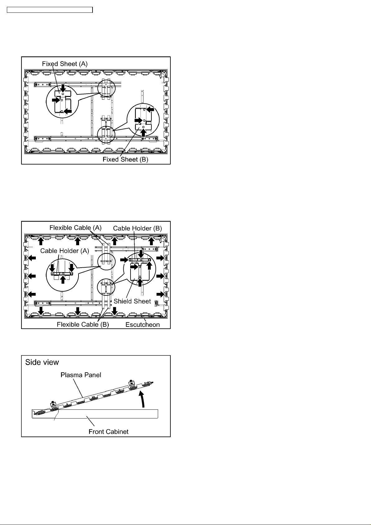
48. Remove the each 3 screws of the Fixed Sheets(A, B) and
then remove the Fixed Sheets(A, B).
49. Remove the 2 screws of the Shield Sheet and then remove
the Shield Sheet.
50. Remove the each 3 screws of the Cable Holders(A, B) and
then remove the Cable Holders(A, B) and the Flexible
Cables(A, B).
51. Remove the 13 screws of the Escutcheon.
52. Pull the bottom of the Plasma Panel forward.
53. Slide the Plasma Panel and then remove the Plasma Panel.
26
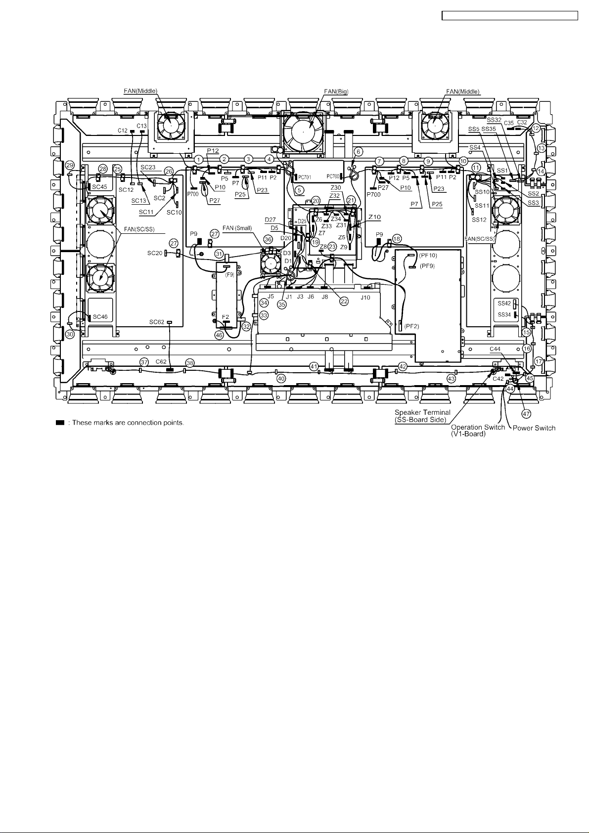
8 Location of Lead Wiring
TH-65PHD7UY / TH-65PHD7EK / TH-65PHD7BK
27
TH-65PHD7UY / TH-65PHD7EK / TH-65PHD7BK
28

9 Adjustment Procedure
TH-65PHD7UY / TH-65PHD7EK / TH-65PHD7BK
9.1. Driver Set-up
9.1.1. Item / Preparation
1. Input an APL 100 % white signal.
2. Set the picture controls as follows.
Picture mode: Normal
White balance: Normal
Aspect: 16:9
9.1.2. Adjustments
Adjust driver section voltages referring the panel data on the
panel data label.
Name Test Point Voltage Volume Remarks
Vsus TPVSUS
(SS)
Ve TPVE (SS) 150V* ± 1V VR6250(SS)
Vset TPVSET
(SC)
Vad TPVAD (SC) -85V ± 1V VR6801(SC)
Vscn TPVSCN
(SC)
Vda TPVDA (SS) 75V ± 1V R665
Vsus2 TPVSUS2
(SC)
Vda2 TPVDA2
(SC)
Vbk TPVBK (SC) 140V ± 1V VR6802
*See the Panel label.
180V* ± 2V R641
230V ± 7V ---
Vad*+120V
±4V
180V ± 2V R641
75V ± 1V R665
(P(SS))
---
(P(SS))
(P(SC))
(P(SC))
(SC)
29
TH-65PHD7UY / TH-65PHD7EK / TH-65PHD7BK
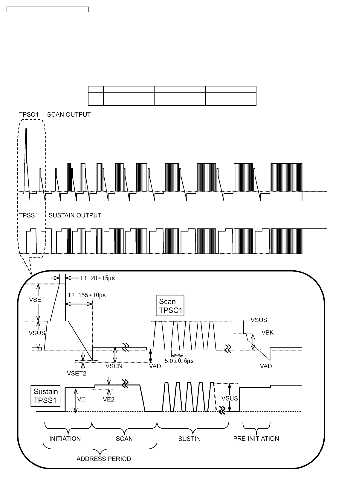
9.2. Initialization Pulse Adjust
1. Input the Cross hatch signal to plasma video input.
2. Set the picture controls as follows.
· Picture mode: Normal
· White balance: Cool
3. Adjust the indicated test point for the specified ware form.
Test point Volume Level
T1 TPSC1 (SC) --- 20 ± 15µ Sec
T2 TPSC1 (SC) VR6602(SC) 155 ± 10µ Sec
30
 Loading...