

Panasonic TH-65LFB70E Schematic
ORDER No. PCZ1406138CE
Service Manual
Touch Screen LCD Display
TH-65LFB70E
LA54 Chassis
This service information is designed for experienced repair technicians only and is not designed for use by the general public. It does not
contain warnings or cautions to advise non-technical individuals of potencial dangers in attempting to service a product. Products
powered by electricity should be serviced or repaired only by experienced professional technicians. Any attempt to service or repair the
product or products deal within this service information by anyone else could result in serious injury or death.
There are special components used in this equipment which are important for safety. These parts are marked in the
Schematic Diagrams, Circuit Board Diagrams, Explorer Views and Replacement Parts List. It is essential that these
critical parts should be replaced with manufacturer´s specified parts to prevent shock, fire or other hazards. Do not
modify the original design without permission of manufacturer.
IMPORTANT SAFETY NOTICE
Warning
© Panasonic Corporation 2014.
Unauthorized copying
distribution is a violation of law.
and

Contents
2
SAFETY PRECAUTIONS ........................................... 3
GENERAL GUIDE LINES ...................................... 3
TOUCH – CURRENT CHECK ............................... 3
PREVENTION OF ELECTROSTATIC DISCHARGE
(ESD) TO ELECTROSTATICALLY SENSITIVE (ES)
DEVICES ................................................................... 4
ABOUT LEAD FREE SOLDER (PBF) ......................... 5
SUGGESTED PB FREE SOLDER ........................ 5
SERVICE NAVIGATION ............................................. 6
CHASSIS BOARD LAYOUT ................................. 6
SERVICE HINTS ........................................................ 7
APPLICABLE INPUT SIGNALS .................................. 8
SPECIFICATIONS .................................................... 10
SERVICE MODE ...................................................... 12
CAT (COMPUTER AIDED TEST) MODE ................. 12
IIC MODE .................................................................. 12
CD MODE ................................................................. 13
NW MODE ................................................................ 14
SD MODE, MS MODE .............................................. 15
ID MODE ................................................................... 16
IIC MODE STRUCTURE...........................................17
SELF CHECK ........................................................... 18
POWER LED BLINKING TIMING CHART ................ 19
LCD PANEL TEST MODE ........................................ 20
DIAGNOSIS FLOW CHART ..................................... 21
DIAGNOSIS OF TOUCH PANEL .............................. 22
WIRING DIAGRAM ................................................... 23
BLOCK DIAGRAM (1 OF 3) ..................................... 24
PARTS LOCATION ................................................... 27
LOCATION OF LEAD WIRING ................................. 31
REPLACEMENT PARTS LIST NOTE ....................... 32
REPLACEMENT PARTS LIST .................................. 33
SCHEMATIC DIAGRAMS NOTE .............................. 88
A-BOARD (1 OF 24) SCHEMATIC DIAGRAM .......... 89
DS-BOARD SCHEMATIC DIAGRAM ..................... 113
HX-BOARD SCHEMATIC DIAGRAM ..................... 114
H1-BOARD SCHEMATIC DIAGRAM ...................... 115
V1-BOARD SCHEMATIC DIAGRAM ...................... 116
V2-BOARD SCHEMATIC DIAGRAM ...................... 117
CONDUCTOR VIEWS ............................................ 118

Safety Precautions
3
General Guide Lines
1. When servicing, observe the original lead dress. If a short circuit is found, replace all parts which have been overheated
or damaged by the short circuit.
2. After servicing, see to it that all the protective devices such as insulation barriers, insulation papers shields are properly
installed.
3. After servicing, make the following touch current checks to prevent the customer from being exposed to shock hazards.
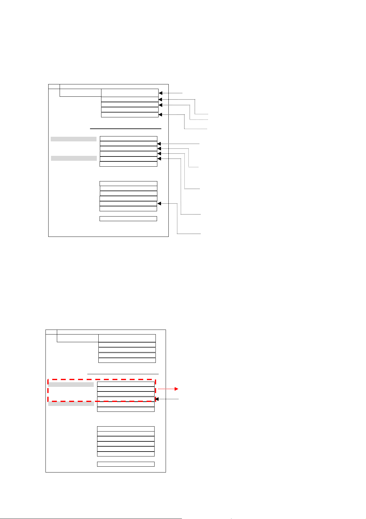
Touch-Current Check
1. Plug the AC cord directly into the AC outlet. Do not use an isolation transformer for this check.
2. Connect a measuring network for touch currents between each exposed metallic part on the set and a good earth
ground such as a water pipe, as shown in Fig. 1.
3. Use Leakage Current Tester (Simpson 228 or equivalent) to measure the potential acr oss the measuring network.
4. Check each exposed metallic part, and measure the voltage at each point.
5. Reserve the AC plug in the AC outlet and repeat each of the above measure.
6. The potential at any point (TOUCH CURRENT) expressed as voltage U1 and U2, does not exceed the following values:
For a. c.: U1 = 35 V (peak) and U2 = 0.35 V (peak);
For d. c.: U1 = 1.0 V,
Note:
The limit value of U2 = 0.35 V (peak) for a. c. and U1 = 1.0 V for d. c. correspond to the values 0.7 mA (peak) a. c. and
2.0 mA d. c.
The limit value U1 = 35 V (peak) for a. c. correspond to the value 70 mA (peak) a. c. for frequencies greater than 100
kHz.
7. In case a measurement is out of the limits specified, there is a possibility of a shock hazard, and the equipment shoul d
be repaired and rechecked before it is returned to the customer.
COLD
WATER PIPE
(EARTH GROUND)
TO
APPLIANCES
EXPOSED
METAL PARTS
Resistance values in ohms ()
V: Voltmetr or oscilloscope
(r.m.s. or peak reading)
NOTE – Appropriate measures should be taken to obtain the correct value in case of non-sinusoidal waveforms
Measuring network for TOUCH CURRENTS
=0.22F
Fig. 1
C
S
10k
(V)
U
1
=1500
R
S
R0=500
Input resistance: 1M
Input capacitance:200pF
Frequency range: 15Hz to 1MHz and d.c.respectively
0.022
F
V
U2 (V)

Prevention of Electrostatic Discharge (ESD) to Electrostatically
4
Sensitive (ES) Devices
Some semiconductor (solid state) devices can be damaged easily by static electricity. Such components commonly are
called Electrostatically Sensitive (ES) Devices. Examples of typical ES devices are integrated circuits and some field-effect
transistors and semiconductor "chip" components. The following techniques should be used to help reduce the incidence of
component damage caused by electrostatic discharge (ESD).
1. Immediately before handling any semiconductor component or semiconductor-equipped assembly, drain off any ESD on
your body by touching a known earth ground. Alternatively, obtain and wear a commercially available discharging ESD
wrist strap, which should be removed for potential shock reasons prior to applying power to the unit under test.
2. After removing an electrical assembly equipped with ES devices, place the assembly on a conductive surface such as
aluminum foil, to prevent electrostatic charge build up or exposure of the assembly.
3. Use only a grounded-tip soldering iron to solder or unsolder ES devices.
4. Use only an anti-static solder removal device. Some solder removal devices not classified as "anti-static (ESD
protected)" can generate electrical charge sufficient to damage ES devices.
5. Do not use freon-propelled chemicals. These can generate electrical charges sufficient to damage ES devices.
6. Do not remove a replacement ES device from its protective package until immediately before you are ready to install it.
(Most replacement ES devices are packaged with leads electrically shorted together by cond uctive foam, aluminum foil
or comparable conductive material).
7. Immediately before removing the protective material from the leads of a replacement ES device, touch the protective
material to the chassis or circuit assembly into which the device will be installed.
Caution
Be sure no power is applied to the chassis or circuit, and observe all other safety precautions.
8. Minimize bodily motions when handling unpackaged replacement ES devices. (Otherwise harmless motion such as th e
brushing together of your clothes fabric or the lifting of your foot from a carpeted floor can generate static electricity
(ESD) sufficient to damage an ES device).
There are special components used in this equipment which are important for safety.
These parts are marked by in schematic diagrams, exploded views and replacement parts list. It is essential that
these critical parts should be replaced with manufacturer’s specified parts to prevent shock, fire, or other hazards. Do
not modify the original design without permission of manufacturer.
IMPORTANT SAFETY NOTICE
About lead free solder (PbF)
5
Note: Lead is listed as (Pb) in the periodic table of elements.
In the information below, Pb will refer to Lead solder, and PbF will refer to Lead Free Solder.
The Lead Free Solder used in our manufacturing process and discussed below is (Sn+Ag+Cu).
That is Tin (Sn), Silver (Ag) and Copper (Cu) although other types are available.
This model uses Pb Free solder in it’s manufacture due to environmental conservation issues. For service and repair work,
we’d suggest the use of Pb free solder as well, although Pb solder may be used.
PCBs manufactured using lead free solder will have the PbF within a leaf Symbol
stamped on the back of PCB.
Caution
Pb free solder has a higher melting point than standard solder. Typically the melting point is 50 ~ 70 °F (30~40°C)
higher. Please use a high temperature soldering iron and set it to 700 ± 20 °F (370 ± 10 °C).
Pb free solder will tend to splash when heated too high (about 1100 °F or 600 °C).
If you must use Pb solder, please completely remove all of the Pb free solder on the pins or solder area before
applying Pb solder. If this is not practical, be sure to heat the Pb free solder until it melts, before applying Pb solder.
After applying PbF solder to double layered boards, please check the component side for excess solder which may
flow onto the opposite side. (see Fig.2)
Suggested Pb free solder
There are several kinds of Pb free solder available for purchase. This product uses Sn+Ag+Cu (tin, silver, copper) solder.
However, Sn+Cu (tin, copper), Sn+Zn+Bi (tin, zinc, bismuth) solder can also be used. (see Fig.3)
Fig.2
Fig.3
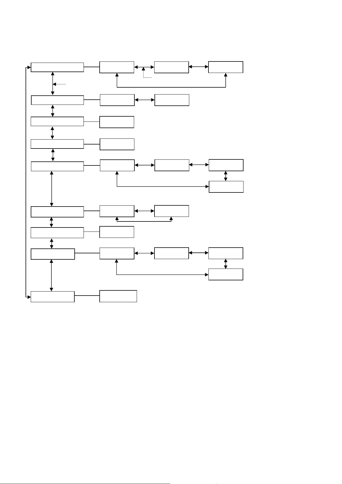
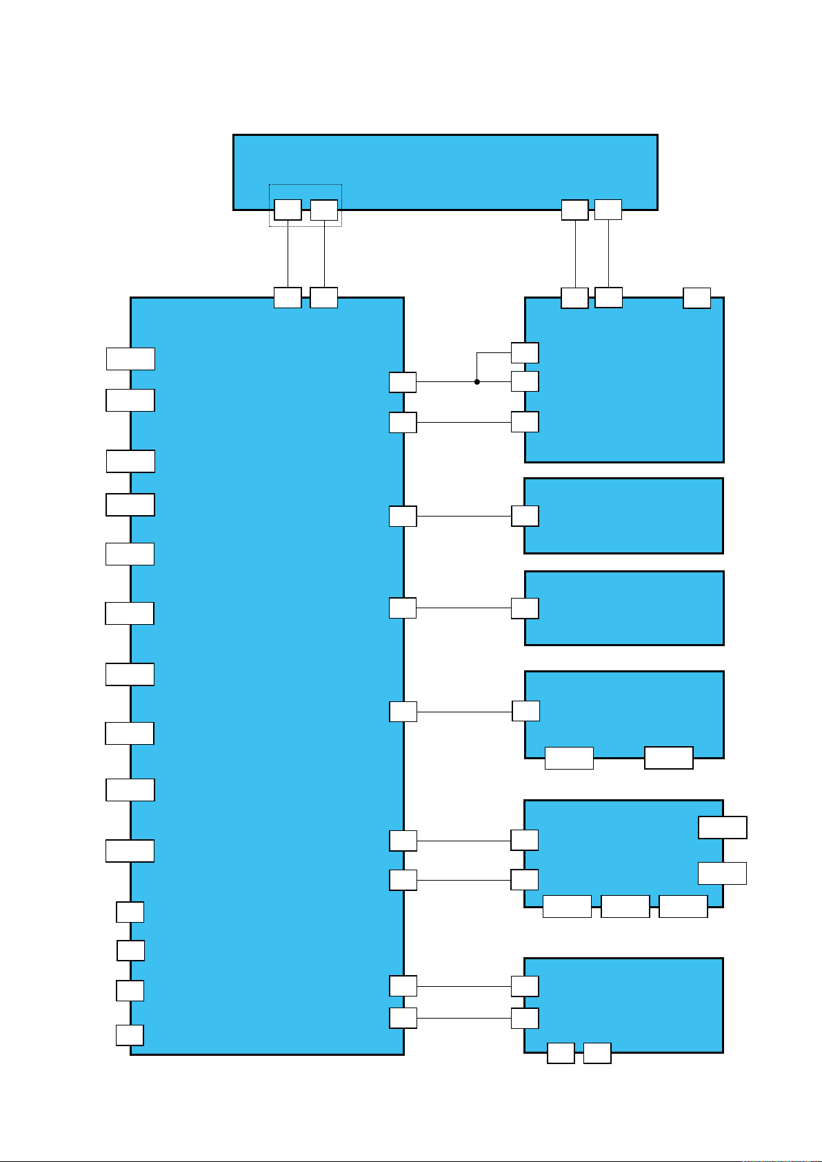
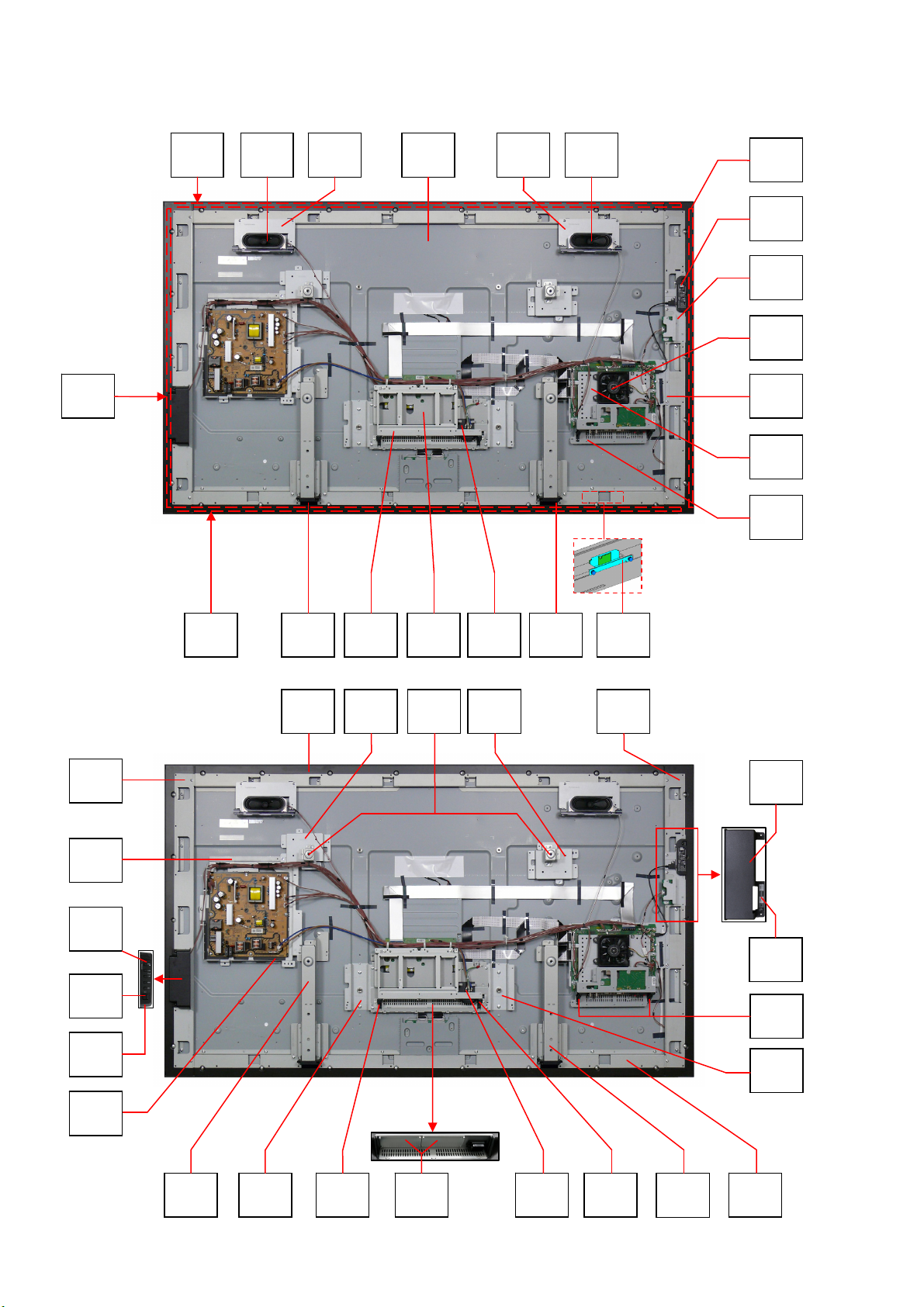
Service Navigation
6
Chassis Board Layout
P-UNIT
V2-BOARD
Board Name Function
A-Board Main Processor, HDMI, DVI-D IN, PC-IN, Audio OUT / IN, Ethernet(LAN),
V2-Board Key control, Power switch
V1-Board Remote Reciever, Power and Timer LED, C.A.T.S
P-Unit Power Supply, Main Input
H1-Board USB Terminal
HX-Board Speakers Out, PC Out, Audio IN, RS-232C input
DS-Board Slot Interface
H1-BOARD
A-BOARD
HX-BOARD
DS-BOARD
WIFI,COMPONENT/RGB-IN, SPI Flash, EEP memory,
V1-BOARD
DDR memory
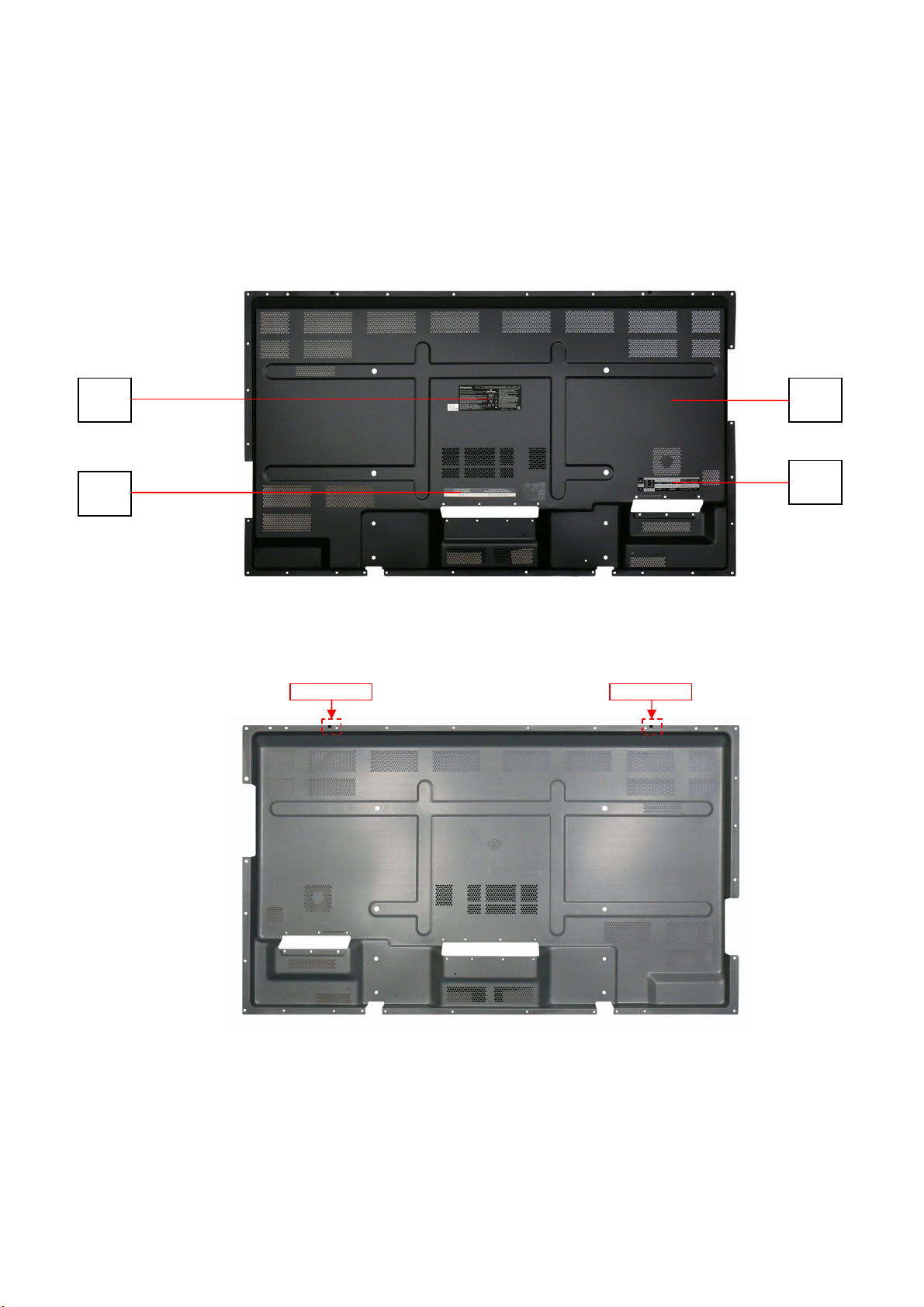
Service Hints
7
How to remove the backcover
Lay the main unit face down. (see Fig.4)
Remove the 44 fixing screws, 4 caps and backcover (see Fig.5)
(1)
(1)
(1)
(1) (1)
(1)
(1) (1) (1) (1) (1) (1) (1)
(3)
(2)
Fig.4
(2) (2) (2)
SCREWS
(1) THEJ025 /30 pcs /
(2) THEL0429 /14 pcs /
(3) TKKL5493 /4 pcs /
(1)
(3)(3)
(2)
(3)
(2)(2)
(1)
(1)
(1)
(1)
(2) (2) (2) (2)
(1)
(1) (1) (1) (1) (1) (1) (1) (1) (1)
(1)
(2)
(2)
(2)
(1)
Fig.5

Applicable Input Signals
8
*Mark: Applicable input signal
Signal name
Horizontal
frequency
(kHz)
Vertical
frequency
(Hz)
COMPONENT /
RGB IN/ PC IN
(Dot clock (MHz)
1 525(480)/60i 15.73 59.94 *(13.5) *(27.0) *
2 525(480)/60p 31.47 59.94 *(27.0) *5 *(27.0) *
3 625(575)/50i 15.63 50.00 *(13.5)
4 625(576)/50i 15.63 50.00 *(27.0) *
5 625(575)/50p 31.25 50.00 *(27.0)
6 625(576)/50p 31.25 50.00 *(27.0) *
7 750(720)/60p 45.00 60.00 *(74.25) *(74.25) *
8 750(720)/50p 37.50 50.00 *(74.25) *(74.25) *
9 1,125(1,080)/60p 67.50 60.00 *(148.5) *1 *(148.5) *
10 1,125(1,080)/60i 33.75 60.00 *(74.25) *1 *(74.25) *
11 1,125(1,080)/50p 56.26 50.00 *(148.5) *1 *(148.5) *
12 1,125(1,080)/50i 28.13 50.00 *(74.25) *1 *(74.25) *
13 1,125(1,080)/24psF 27.00 48.00 *(74.25) *2
14 1,125(1,080)/30p 33.75 30.00 *(74.25) *1 *(74.25)
15 1,125(1,080)/25p 28.13 25.00 *(74.25) *1 *(74.25)
16 1,125(1,080)/24p 27.00 24.00 *(74.25) *1 *(74.25) *
17 1,125(1,080)/50i 31.25 50.00 *(74.25) *3
18 2,048x1,080/24psF *7 27.00 48.00
19 2,048x1,080/24p *7 27.00 24.00
20 640x400@70Hz 31.46 70.07 *(25.17)
21 640x480@60Hz 31.47 59.94 *(25.18) *6 *(25.18) *
22 640x480@72Hz 37.86 72.81 *(31.5)
23 640x480@75Hz 37.50 75.00 *(31.5)
24 640x480@85Hz 43.27 85.01 *(36.0)
25 800x600@56Hz 35.16 56.25 *(36.0)
26 800x600@60Hz 37.88 60.32 *(40.0) *(40.0) *
27 800x600@72Hz 48.08 72.19 *(50.0)
28 800x600@75Hz 46.88 75.00 *(49.5)
29 800x600@85Hz 53.67 85.06 *(56.25)
30 852x480@60Hz 31.47 59.94 *(33.54) *6 *(34.24) *
31 1,024x768@50Hz 39.55 50.00 *(51.89) *
32 1,024x768@60Hz 48.36 60.00 *(65.0) *(65.0) *
33 1,024x768@70Hz 56.48 70.07 *(75.0)
34 1,024x768@75Hz 60.02 75.03 *(78.75)
35 1,024x768@85Hz 68.68 85.00 *(94.5)
36 1,066x600@60Hz 37.64 59.94 *(53.0) *(53.0) *
37 1,152x864@60Hz 53.70 60.00 *(81.62) *
38 1,152x864@75Hz 67.50 75.00 *(108.0)
39 1,280x768@60Hz 47.70 60.00 *(80.14)
40 1,280x800@60Hz (1) 49.31 59.91 *(71.0) *(71.0) *
41 1,280x800@60Hz (2) 49.70 59.81 *(83.5) *(83.5) *
42 1,280x960@60Hz 60.00 60.00 *(108.0)
43 1,280x960@85Hz 85.94 85.00 *(148.5)
44 1,280x1,024@60Hz 63.98 60.02 *(108.0) *(108.0) *
45 1,280x1,024@75Hz 79.98 75.03 *(135.0)
46 1,280x1,024@85Hz 91.15 85.02 *(157.5)
47 1,366x768@50Hz 39.55 50.00 *(69.92) *
48 1,366x768@60Hz 48.36 60.00 *(86.71) *(87.44) *
49 1,400x1,050@60Hz 65.22 60.00 *(122.61) *
50 1,440x900@60Hz (1) 55.47 59.90 *(88.75) *(88.75) *
51 1,440x900@60Hz (2) 55.93 59.89 *(106.5) *(106.5) *
52 1,600x1,200@60Hz 75.00 60.00 *(162.0) *(162.0) *
53 1,600x1,200@65Hz 81.25 65.00 *(175.5)
54 1,920x1,080@60Hz 67.50 60.00 *(148.5) *4 *(148.5) *
55 1,920x1,200@60Hz 74.04 59.95 *(154.0) *
56 Macintosh 13‘‘ (640 x 480) 35.00 66.67 *(30.24)
57 Macintosh 16‘‘ (832 x 624) 49.72 74.54 *(57.28)
58 Macintosh 21‘‘ (1,152 x 870) 68.68 75.06 *(100.0)
DVI-D IN
(Dot clock (MHz)
HDMI

*1: Based on SMPTE 274M standard.
9
*2: Based on SMPTE RP211 standard.
*3: Based on SMPTE 295M standard.
*4: The input signal is recognized as 1,125 (1,080) / 60p.
*5: When selected the RGB format and 525p signal input to the PC IN terminal, it is recognized as VGA 60 Hz signal.
*6: When inputted VGA 60Hz format signal from the other than PC IN terminal, it is recognized as 525p signal.
*7: Based on SMPTE 292M and 372M standards. These signals can be received when the Dual Link HD-SDI Terminal
Board (TY-FB11DHD) is installed.
Note: Signals without above specifications may not be displayed properly.

Specifications
10
Power Source: 220-240V AC, 50 / 60Hz
Rated Power Consumption: 215W
Stand-by Power Consumption: 0.5W
Operating Conditions: Temperature: 0°C 40°C
Humidity: 20% 80% RH (non condensing)
Applicable signals:
Colour System NTSC, PAL, PAL60, SECAM, Modified NTSC
Scanning Format 525(480) / 60i • 60p, 625(575) / 50i • 50p, 750(720) / 60p• 50p
1125(1080) / 60i • 60p • 50i • 50p • 24p • 25p • 30p • 24psF, 1250 (1080) / 50i
PC signal VGA, SVGA, XGA, SXGA, UXGA . . . . . (compressed)
Horizontal scanning frequency 15 - 110kHz
Vertical scanning freguency 48 - 120Hz
Terminals:
AV IN
VIDEO BNC 1.0 Vp-p (75
AUDIO 1 IN Stereo mini jack (M3) x 1 0.5 Vrms, Shared with COMPONENT/RGB IN
HDMI 1 TYPE A Connector x 2
HDMI 2
COMPONENT/RGB IN
Y/G BNC with sync 1.0 Vp-p (75
Pb/Cb/B BNC 0.7 Vp-p (75
Pr/Cr/R BNC 0.7 Vp-p (75
AUDIO 1 IN Stereo mini jack (M3) x 1 0.5 Vrms, Shared with VIDEO
DVI-D IN
DVI-D 24Pin Compliance with DVI Revision 1.0
Content Protection Compatible with HDCP 1.1
AUDIO 2 IN Stereo mini jack (M3) x 1 0.5 Vrms, Shared with PC IN
PC IN
High-Density Mini D-sub 15 Pin Y or G with sync 1.0 Vp-p (75
Y or G without sync 0.7 Vp-p (75
Pb/Cb/B: 0.7 Vp-p (75
Pr/Cr/B: 0.7 Vp-p (75
HD/VD: 1.0 – 5.0 Vp-p (high impedance)
AUDIO 2 IN Stereo mini jack (M3) x 1 0.5 Vrms, Shared with DVI-D IN
SERIAL External Control Terminal
D-sub 9 Pin RS-232C compatible
PC OUT R: 0.7 Vp-p (75
G: 0.7 Vp-p (75
B: 0.7 Vp-p (75
HD/VD: 1.0 – 5.0 Vp-p
USB (VIEWER) TYPE A USB connector
USB (TOUCH) TYPE B USB connector
DIGITAL LINK / LAN For RJ45 network and DIGITAL LINK connections, compatible with PJLink™
Communication method: RJ45 100BASE-TX
EXT SP 8
Sound:
Speakers 120mm x 40mm x 2pcs
Audio Output 20W [10W + 10W] (10% THD)
, 20W [10W + 10W] (10% THD)
)
)
)
)
)
)
)
)
)
)
)

11
LCD screen: L5EDDYY00643
1920 x 1080, 16:9
Visible Diagonal 1638mm
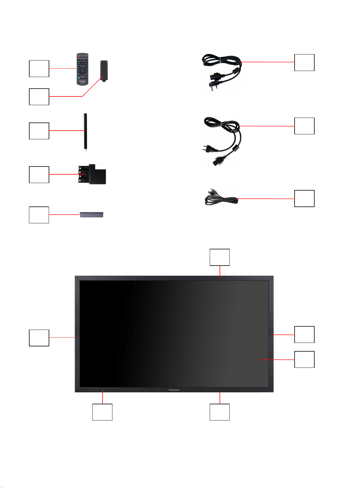
Accessories supplied : Remote Control
2 x R6 (UM3) Batteries
2 xPen
Pen Tray
Eraser
USB Cable
Dimensions: Width: Height: Depth:
1,517mm 892mm 106mm
Mass: 58.0kg
Design and Specifications are subject to change without notice. Mass and dimensions shown are approximate.
This equipment complies with the EMC standards listed below:
EN61000-3-2, EN61000-3-3, EN55022, EN55024

Service Mode
A
12
CAT (Computer Aided Test) Mode
CAT mode menu
CAT panel sys. 8.2
IIC Mode
CD Mode
NW Mode
SD Mode
MS Mode
ID mode
Mode Function Access Button
IIC Mode Service Alignment Action
CD (Complete
Diagnostic)
NW Mode LAN terminal check Action
SD (Status Display) MTBF parameter Action
MS Mode Market Select Mute
ID Mode LSI Check Mute
Software version
information EEPROM edit
Remote Control
Mute
more than 3 seconds
more than 3 seconds
more than 3 seconds
MUTE
VOL Up/Down
Up/Down
R
Left/Right
CTION
RECALL
How to access the CAT mode.
Method A Main unit + remote control operation
Press and hold the button on the right side of the unit and press
the RECALL button on the remote kontrol 3 times quickly within 2
seconds, this will placet he unit into the CAT mode.
Method B Remote control operation only
1. Set OFF timer except fot [0] minute by OFF TIMER button.
(30 minutes, 60 minutes, 90 minutes)
2. Set the volume level of sound to 0 by VOL down button / -button.
3. Set the RECALL button more than 3 seconds before a volume
display disappears.
To exit CAT mode, turn the power off by main unit or a remote control.
IIC Mode
Select the IIC mode by Up/Down buton on the remote control at the front page of CAT mode and then press the Action
button on the remote control.
OSD
Y 525/480)/60p
16:9 STANDARD Mid
LCD W/B Adj.
R Drive
FE FE
Subject and Item are mentioned on “IIC mode structure”.
To exit the IIC mode, press the R button on remote control.
Original data
on remote control.
on the remote control.
Subject
Item
on the remote control.
Subject (or Items).
New data
on the remote control or change the alignment
How to access the CAT mode.
1. Select the alignment Subject by Up/Down buttons
2. Select the alignment Item by Left/Right buttons
3. Adjust optimum setting by Volume Up/Down buttons
4. The data is memorized when press the R button

CD Mode
A
13
Select the CD mode by Up/Down buton on the remote control at the front page of CAT mode and then press the Mute
button on the remote control more than 3 seconds.
CD
MONITOR-MCU(50inch) *.****LFB70 OK
MONITOR-EEPROM **.** * BB 73
MONITOR-EEPROM Change Addr 00 01
Data 01 01
MONITOR-FPGA **.**
MONITOR-FRC **
LAN MCU **.**/**.**
HD-BaseT **.**.***
TOUCH PANEL *.*.*.*
LAN-MAC (WIRED) **:**:**:**:**:**
LAN-MAC (WIRELESS) **:**:**:**:**:**
SLOT BOARD EEPROM -- -- -- --
SLOT BOARD --/--/-- -- -- -SERIAL No **********
PTCT 01. 02. 03. 04. 05.
Memory data change
ddress
PTCT position: [01] [02] [03] [04] [05]
0
0
Change by Up/Down buttons on the remote control.
Factory use
New data
Original data
SOS history
Data
Change by Left/Right buttons on the remote control.
0
0
Change by VOL Up/Down buttons on the remote control.
The data is memorized when switch off the main power.
To exit the CD mode, press the R button on the remote control.
About the serial number display
As for the serial number of A-module for repair, a dummy value is displayed.
* By the set for which A-module was exchanged, a serial number is displayed as [-----]
About the history display of SOS for the power supply system
This unit adds the history display (5 times) of power supply failure to the CD mode as PTCT.
By the self check of a signal system, only one history is displayed (After a self check disappears). But PTCT display
5 times of histories (Abnormality of the latest 3 times. First time and second time after shipment) and after a self
check does not disappear.
You can see a detailed history of power failure sometimes.
*About the display contents of PTCT
PTCT : The position of [05] is the first time after shipment.
PTCT : The position of [04] is the second time after shipment.
PTCT : The position of [03] is second from last time.
PTCT : The position of [02] is last time.
PTCT : The position of [01] is the latest.
In [Contents & Check point] of [6.1.2 Power LED Blinking timing chart], the two-digit following PTCT are displayed
by a hexadecimal number.
Blinking times Contents &Check point Display contents
Ex. 1 4 times PTCT 04 H09 04
Ex. 2 8 times PTCT 08 H029 08
NW Mode
14
Note:
To use the network function, set each “Network Setup” setting and make sure to set the “Control I/F” to “LAN”
or “RS232C”
Select the NW mode by Up/Down buton on the remote control at the front page of CAT mode and then press the Action
button on the remote control.
NW
TEST OK
Version xx.xx/xx.xx
MAC(WIRED) xx:xx:xx:xx:xx:xx
MAC(WIRELESS) xx:xx:xx:xx:xx:xx
Control I/F Select xxxxxxxxxxxxxxx
DIGITAL LINK
Firmware xx.xx.xxx
*1
Link Status No link
HDMI Status HDMI on
BER V_/A_/B_/C_
*2
Max Count A X/B X/C X/D X
Est. Cable Length x (m)
Signal Quality
A - xx (dB)
B - xx (dB)
C - xx (dB)
D - xx (dB)
Min - xx (dB)
Max - xx (dB)
Model Name xxxxxxxx
*1: If you move a cursor to “Firmware” and press an Action button, “Only receiving side information display” and
“Receiving side / Transmitting side information simultaneous display” can be s witched.
*2: The value of “Max Count” is resettable if you move a cursor to “Max Count” and press an Action butto n.
[Example of Receiving / Transmitting side information simultaneous display]
NW
TEST OK
Version xx.xx/xx.xx
MAC(WIRED) xx:xx:xx:xx:xx:xx
MAC(WIRELESS) xx:xx:xx:xx:xx:xx
Control I/F Select xxxxxxxxxxxxxxx
DIGITAL LINK
Firmware xx.xx.xxx / xx.xx.xxx
Link Status DIGITAL LINK/DIGITAL LINK
HDMI Status HDMI on / HDMI on
BER V_/A_/B_/C_/T_
Max Count A X/B X/C X/D X
Est. Cable Length x (m)
Signal Quality
A - xx (dB)
B - xx (dB)
C - xx (dB)
D - xx (dB)
Min - xx (dB)
Max - xx (dB)
Model Name xxxxxxxx
To exit the NW mode, press the R button on the remote control.
Press the Action button to start TEST (Check of Ping).
Check to show “OK” in TEST column.
If “G_NG” shows, it is failure for Ping process.
If “L_NG” shows, it is failure for Link process.
Software Version
Mac address
Control I/F Select
DIGITAL LINK: Checking signal quality
Link Status : Connection state
No link : No connection
DIGITAL LINK : In DIGITAL LINK operation
Ethernet : In Ethernal operation
HDMI Status : Display the information of HDMI ON/OFF and HDCP
No HDMI : Can not be recognized as a signal of the HDMI
HDMI on : Non HDCP HDMI signal
HDCP on : HDCP HDMI signal
Error ratio of the transmission path information
V : VIDEO BER
A : AUDIO BER
B : BLANK BER
C : CONTROL BER (Max: 10)
Standard of momentary signal quality aggravation
When it is over 64, the imagine may have broken off.
(Max: 255)
Signal Quality: Display the signal quality at the time of
DIGITAL LINK operation
OK/LOW/NG is displayed as each
Channel (A,B,C,D, Min, Max)
-12 dB or more : Normal receivable range
-11 to -8 dB : Partial damage of data (possible image output)
-7 dBor less : Synchronization disorder occurrence
(impossible image output)
Transmitting side information is displayed on right-hand side.
T: total ber (Transmitting side)
SD Mode
15
Select the SD mode by Up/Down button on the remote control at the front page of CAT mode and then press
the Action button on the remote control.
OSD
SD
Input command
check
MTBF Parameter WT PT
TE
Condition
Sensor
Remote Control Mode A B
To exit the SD mode, press the R button on the remote control.
** ** ** ** ** ** **
** ** ** ** ** ** **
** ** ** ** ** **
**
*
+**
---
BL
**
***
History of remote control command.
(Factory use).
Cumulative Time for power on condition. (unit :hour)
Counter of power on. (unit :time)
Counter of backlight OFF during abnormally high temperature(unit:time)
Temperature (unit :degrees)
Backlight Limit Value
Illumination sensor value
MS Mode
Select the MS mode by Up/Down button on the remote control at the front page of CAT mode and then press the Mute
button on the remote control more than 3 seconds.
MS
Market select **.** 2 2
Change by Left/Right buttons on the
remote control and press the action button
Present number
EEPROM data version
To exit the MS mode, press the R button on the remote control.
Caution:
Market Select should be set after exchange of A-Board.
Destination number:
Number Destination
0 Japan
1 US(North America)
2 Europe
3 Asia,
Oceania,ME,Africa
18 China

ID Mode
16
Select the ID mode by Up/Down button on the remote control at the front page of CAT mode and then press the Mute
button on the remote control more than 3 seconds.
ID
A H90MEM1 OK DS H51RTC OK
H65AVSW OK
H61ADV OK
H62TEMP OK
H63CPG OK
H66HDMIRX OK
H93LAN OK
H92MEM2 OK
H56LVDSRX OK
H67DLK OK
H68FRC OK
To exit the ID mode, press the R button on the remote control.
IIC1
IIC2
IIC3
IIC4
IIC Mode Structure
17
(following items value is sample data)
Panel W/B Adj.
R DRIVE
FE
by up / down button
DIGITAL LINK Update
Update Not
Ready
EDID Write Protect
Protect
Front Panel key Check
Key Check --
PICTURE Sub Adjust
Main Contrast1
0
G DRIVE
FC
by left / right button
Update Ready
R sub Bright1
0
B DRIVE
FA
G sub Bright1
0
TEMP CONTROL Adj
Chroma Control
Pos./Size
Aging
B sub Bright1
0
Threshold Temp
52
GUN OFF
0
H Position
81
Panel Color
White + Time, Temperature
WHITE
RED
GREEN
BLUE
BLACK
These are selected by Action buton of Remote control and press the R button to exit.
Offset Temp
3
V Position
80
WHITE Ramp
RED Ramp
GREEN Ramp
BLUE Ramp
Color Bar
Scrolling Vertical Window
H Size
80
B DRIVE
00

Self Check
18
Display Indication
1. Self check is used to automatically check the bus line controlled circuit of the LCD display.
2. To get into the Self check mode, press the volume down button on the customer controls at the right side of the set, at the
same time pressing the OFF TIMER button on the remote control, and the screen will show.
Method A Self-Check only ( A shipment setup is not carried out )
Select ID mode by UP/Down button on the remote control at the front page of CAT mode and then press the Mute button
on the remote control more then 3 seconds.
Method B Self-Check + Shipment setup
Press and hold the volume down button on the right side of the unit and press the OFF-TIMER button on the remote
control.
If the IIC ports have been checked and found to be incorret, or not located then “- -” will appear in place “OK”
“01” in the lie of the “PTCP” means the number of blinks of the Power LED is 1. (Reference_Power LED blinking timing
chart)
“H09” in the line of the “PTCP” is the error code
To exit the CAT mode switch off the main power.
Note:
The line of the “PTCP” display when you get into the Self check mode for first time only after the Power LED blinks.
ID
A H90MEM1 OK DS H51RTC OK
H65AVSW OK
H61ADV OK
H62TEMP OK
H63CPG OK
H66HDMIRX OK
H93LAN OK
H92MEM2 OK
H56LVDSRX OK
H67DLK OK
H68FRC OK
IIC1
IIC2
IIC3
IIC4
Power LED blinking timing chart
19
1. Subject
Information of LED Flashing timing chart.
2. Contents
When abnormality has occurred the unit, the protection circuit operates and reset to the stand by mode. At this time, the
defective block can be identified by number of blinking of the Power LED on the front panel of the unit.
Blinking times Contents & Check point Check point
1
2
4
8
10
11
13
PTCT 01 H09]*
PANEL SOS
(PTCT E2 H09)*
POWER SOS
(PTCT 04 H09)*
POWER SOS
(PTCT 04 H09)
PANEL 12V SOS
(PTCT 0A H09)
FRC SOS
(PTCT 0B H09)*
FAN SOS
(PTCT 0B H09)
FAN SOS
(PTCT 0D H09)*
REGULATOR SOS (A2 SOS)
(PTCT 1D H09)*
REGULATOR SOS (5V SOS)
(PTCT 2D H09)*
REGULATOR SOS (A2 SOS)
LCD PANEL
P-Board
A-Board
A-Board
LCD Panel
A-Board
DS-Board
SLOT Board
FAN
A-Board
A-Board
(PTCT 4D H09)*
AUDIO SOS

LCD Panel test mode
20
The failure-diagnosis by LCD Panel test mode
To find the possible failure point where in LCD Panel or Printed Circuit Board when the abnormal picture is displa yed.
How to display the test pattern:
(A) Main unit + remote control operation
1. While pressing [VOLUME (-)] button of the main unit, press [R] button of the remote control three times within 2 seconds.
2. Test pattern is displayed and Power LED lights red and orange alternately.
How to Exit: Turn off the unit.
(B) Remote control only
1. Press [Recall] button of the remote control.
2. Press [R] button of the remote control.
3. Press [N] button of the remote control for over 3 seconds.
4. Test pattern is displayed and Power LED lights red and orange alternately.
How to Exit: The unit automatically turns off after around 10 seconds.
[Display pattern]
It is unfixed from which color it starts.
WHITE MAGENTA YELLOW CYAN BLACK
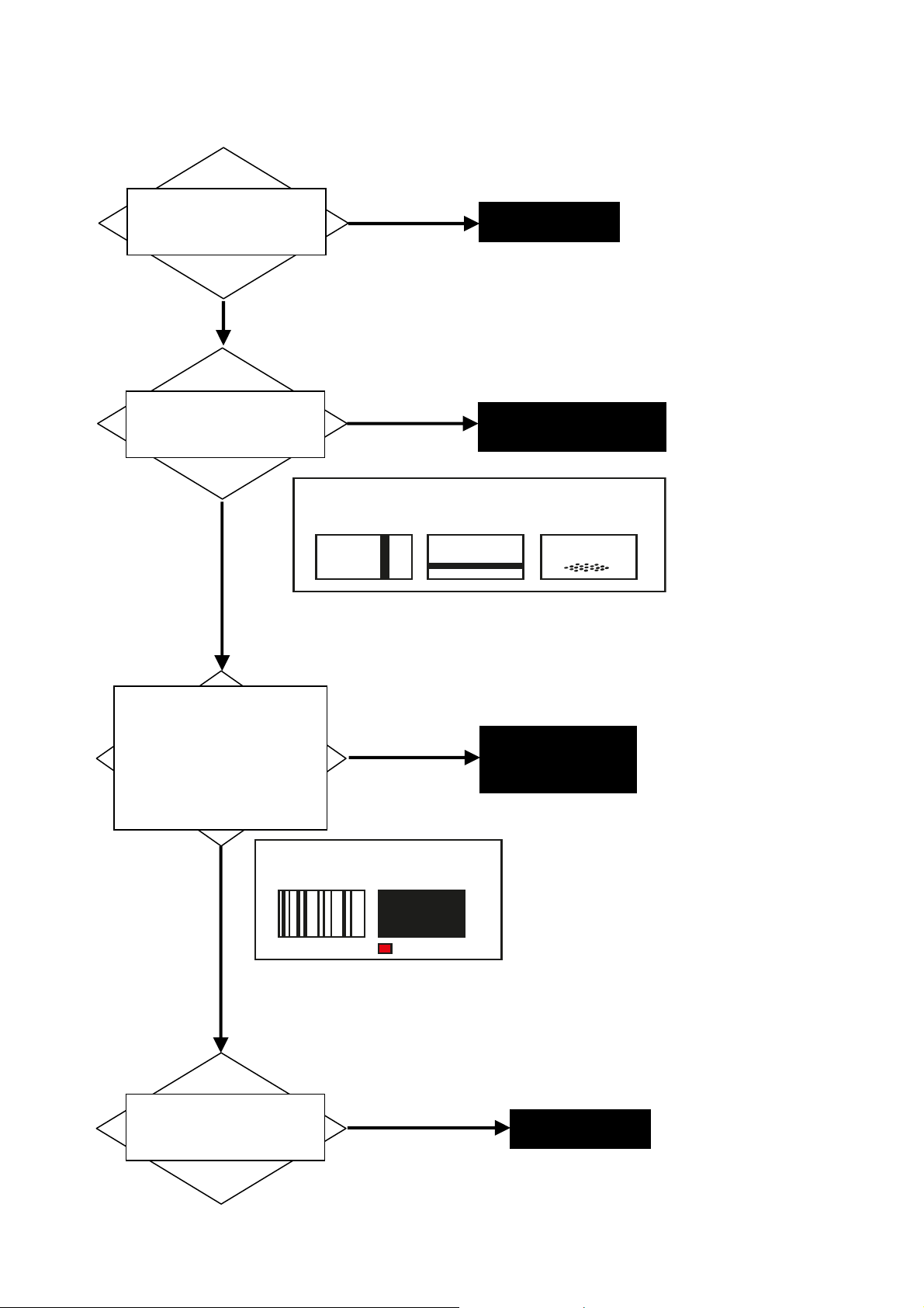
Diagnosis flow chart
21
Is a test pattern
displayed normally?
Yes
It displays.
Failure of A-Board
No
It is still abnormal.
Is a part abnormal
even in test pattern?
Yes
It is abnormal.
Failure of LCD Panel
(rarely failure of A-Board)
Vertical line Horizontal line Color
Vertical bar Horizontal bar unevenness
No
This is not an abnormality of part
-Is the whole abnormal
even in a test pattern?
or
-A test pattern is not displayed
but is the state of LED blink of
red and orange?
Yes
It is abnormal.
Yes
It is blinking.
Failure of A-Board
or
Rarely LCD Panel
Vertical line/ An image is
Vertical bar not displayed
LED blinking
No
- The whole is not abnormal.
- It is not blinking.
A test pattern is not
displayed but is the state
of LED green lighting?
Yes
It is green lighting.
Failure of A-Board

Diagnosis of Touch Panel
22
When a touch panel does not work, narrowing down of the failure part of a setup, and a touch panel or A-Board can be
performed.
Is a touch panel setting
carried out?
No
Check Touch Panel setting
Yes
Is the motion picture of a
USB memory played back?
Yes
Failure of touch panel
No
Failure of A-Board
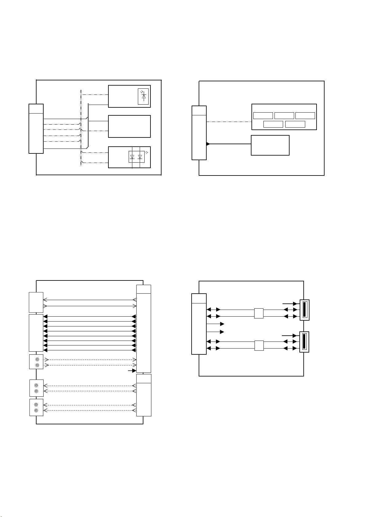
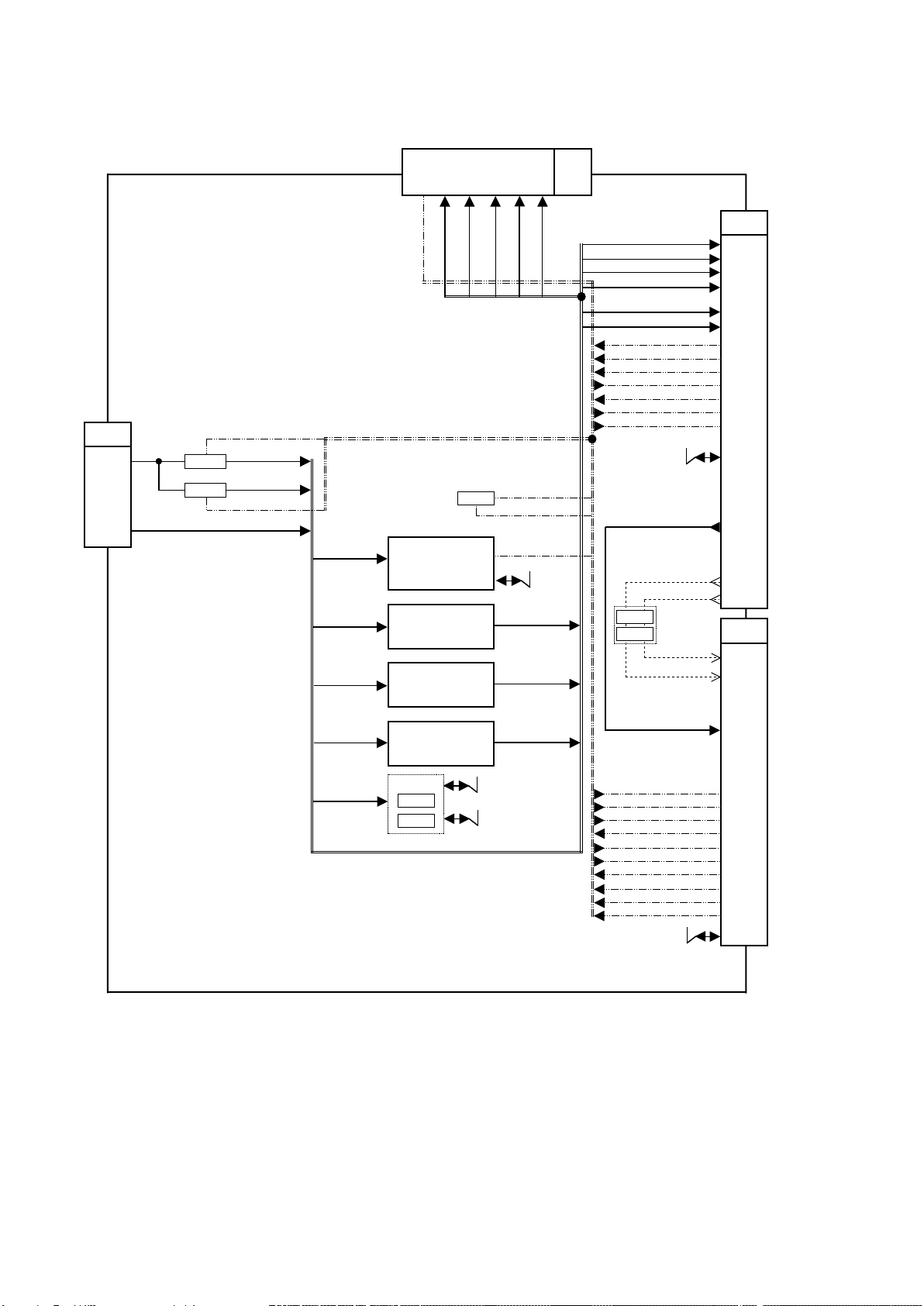
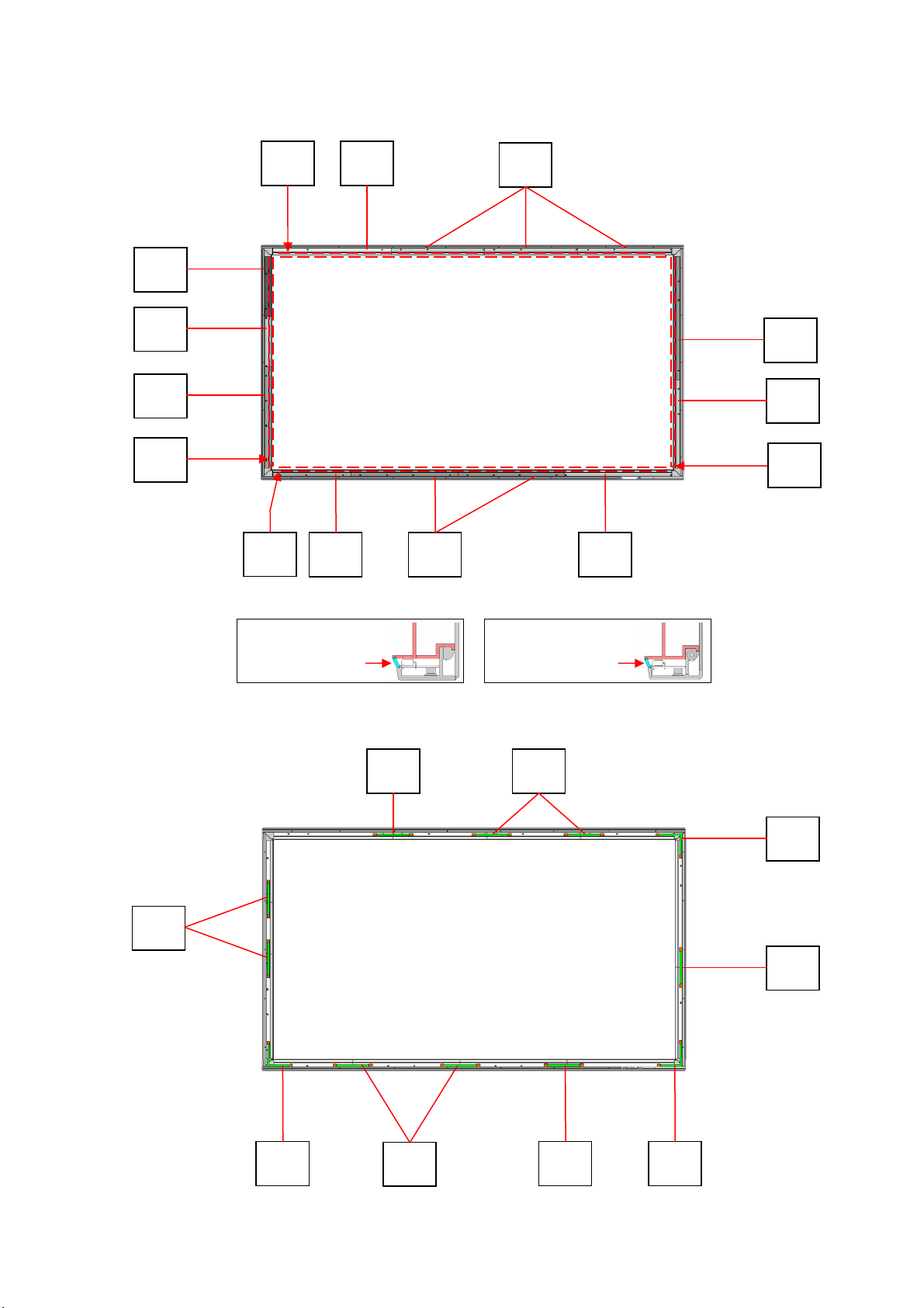
Wiring Diagram
23
A1
TCON
A2
LCD PANEL
P3
P4
MAIN IN
P1
SERVICE
SERVICE
WIFI
ETHERNET
HDMI2
HDMI1
DVI
PC IN
YUV
VIDEO IN
RCA
CN4002
CN2703
JK4801
JK2701
JK2107
JK4004
JK2106
JK2105
JK2104
JK2103
A-BOARD
A5
A4
A22
A11
A47
P2
P5
P6
V22
V11
H47
P-UNIT
V2-BOARD
V1-BOARD
H1-BOARD
JK3802
USB1
JK3801
USB2
Audio IN
FAN
SERVICE
TOUCH
JK2101
A17SPK
A7
A40
A57
A27
A37
A10
A13
HX27
HX37
DS10
DS13
HX-BOARD
JK3501
RS-232C
Input
DS-BOARD
DS3
DS2
JK3502
PC OUT
JK3504
SP_out_L
JK3503
SP_out_R
JK3506
Audio IN
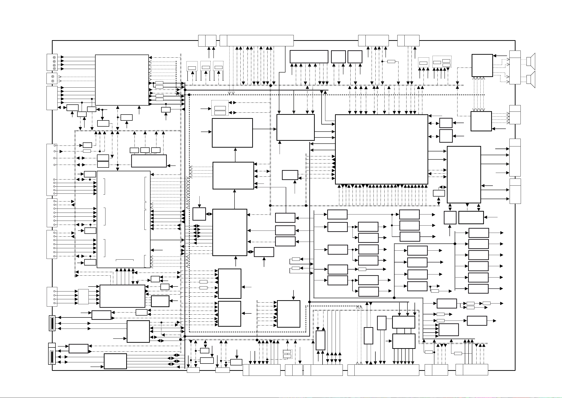
Block Diagram (1/3)
24
A-BOARD
Y,PB,PR
JK2103
V
R
Audio IN
JK2101
PC
13
14
JK2104
12,15
DVI
JK2105
HDMI1
JK2106
HDMI2
JK2107
JK2701
ETHERNET
WIFI
JK4801
A57
TOUCH
CVBS
AUDIO_L_M3
L
AUDIO_R_M3
1
2
3
SDA,SCL
IIC_CONT
SDA1,SCL1
SDA2,SCL2
DDCD_SDA,SCL
TMDS_RXC_P/N
TMDS_RX0_P/N
TMDS_RX1_P/N
TMDS_RX2_P/N
HDMI1_DET
HPD1
HDMI1_CK_P/N
HDMI1_0_P/N
HDMI1_1_P/N
HDMI1_2_P/N
HDMI1_SDA,SCL
HDMI2_DET
HPD2
HDMI2_CK_P/N
HDMI2_0_P/N
HDMI2_1_P/N
HDMI2_2_P/N
HDMI2_SDA,SCL
HDBT_0
HDBT_1
HDBT_2
HDBT-3
1
2
3
F5V
1
2
3
PR_COMP
PB_COMP
Y_COMP
R_PC
G_PC
B_PC
HS_PC
VS_PC
IC2103
EEPROM
1
6
5V
IC2109
Logic IC
DPMS_
V D_SCX1
5V
5V
5V
HDBT_5VDET
HDBT_HPDT
T2701
IC4812
SW
STB3.3V
IC2112
SW
L2121
IC2110
EEPROM
IC2101
EEPROM
IC2102
EEPROM
F5V
3
4
IC2108
Logic IC
DPMS_
HD_SCX1
LAN3.3V
LAN1.8V
LAN1.0V
S3.3VLAN
100
IIC_CONT
1
6
USBP3_N
USBP3_P
97
93
95
17
62
63
3
1
99
2
STB3.3V
IC4006
EEPROM
DVI_DET
IC2104
Logic IC
IC2111
Logic IC
G4,F4
B5,A5
B4,A4
B3,A3
B2,A2
D2,D1
E2,E1
F2,F1
G2,G1
H4,J4
J2,J1
K2,K1
L2,L1
M2,M1
P4,R4
W3,Y3
Y4,W4
W8,Y8
Y9,W9
IC4803
DVI_DET2
DIGITAL INPUT
DIGITAL INPUT
DIGITAL INPUT
SW
7
8
C1AB00003384
AV SWITCH
28,29
3V_SDA1,SCL1
C1AB00003048
Y18
Y19
IC2701
TRANSMITTER/
RECEIVER
3
4
S3.3VLAN
IC4813
Multiplexer
IC2105
IC4009
Temp Sensor
P3V_SDA2,SCL2
F3V_SDA2,SCL2
IIC2
IC2509
AD AV
DIGITAL INPUT
P2,P1
R2,R1
HDBT_1_+/-
HDBT_0_+/-
HDBT_CK_+/-
L19,L20
N19,N20
VS100
SCX_USBOC2
USBP2_N
USBP2_P
1
2
3
4
9
3.3V
IC4019
Logic IC
10,11
T2,T1
U2,U1
HDBT_2_+/-
U19,U20
R19,R20
3
4
IC4802
[C1CB00003456]
USB 2.0HUB
USB_DP1
USB_DM1
USBP4_P
USBP4_N
USB_VBUS1
31
42,43
5V
9V
3.3V
28M_CLK2
CLKM_20MHz
IC4004
Logic IC
8
9
Clock Generator
M23
M22
AUDIO OUTPUT
Input
Sound
Analog
VIDEO
AUDIO INPUT
DIGITAL OUTPUT
VIDEO
Input
DTV Sound
T4,U4
IIC0_SDA,SCL
R1
B12
A11,B11
W19,Y20
A12
G1
D1
F1
E1
1
IC4815
4
Logic IC
2
Controller
18
67
66
59
58
49
50
32
34
33
35
CVBS_OUT
IC4013
C15
N23
N22
R23
R22
P23
P22
A21
B21
A14
A15
A12
A13
D13
D12
U20
T20
N20
N21
HDBT_SDA,SCL
IC4014
Reset IC
RESET_IN
CS
1
SDA
2
MO
5
SCL
6
27
30
31
1
2
AUDIO_R_DS
AUDIO_L_DS
AUDIO_R_M3_2
AUDIO_L_M3_2
Q2503
RGB_CVBS
Q2504
Q2502
R/PR_OUT
Q2501
IC2114
Logic IC
3.3V
28M_CLK
SPG_RESET
IC4020
Logic IC
2
12,7,4
R(9:0), G(9:0), B(9:0)
Control
1.8V,3.3V
3V_SDA4,SCL4
IC2702
Logic IC
IC2704
SPI FLASH
SCX_USBPSW2
USB_DM0
USB_DP0
USB_VBUS0
SCX_USBPSW3
S2_DET
AUD_R
AUD_L
G/Y_OUT
ADV_HD
ADV_VD
B/PB_OUT
ANMPIN
CLAMPY
F3.3V
28M_CLK
PWM2_SQ_L-
PWM2_SQ_L+
PWM2_SQ_R-
PWM2_SQ_R+
PWM_SQ_L-
PWM_SQ_L+
PWM_SQ_R-
PWM_SQ_R+
AUD_R
AUD_L
G/Y_OUT
RGB_CVBS
B/PB_OUT
R/PR_OUT
ADV_HD
ADV_VD
SPDIF1
SDIN1
BCLK1
LRCLK1
PWR5V
STB3.3V
3V3
PMS_TX
PMS_RX
3V3
WL_EN
USB_PWR
USB_OC
USBP1_N
USBP1_P
SCX_USBOC3
SW_5V
Q2327
PWR5V
15V_ON/OFF
PMS_RX
PMS_TX
IIC_INT
3V_SCL4,SDA4
STB5V
4,3 5
1
CN4002
TO DS13
A13
PWR15V
SW_15V
Q2318
5V
PWR15V
15V_ON/OFF
STB5V
3.3V
SPDIF1
SDIN1
BCLK1
LRCLK1
S1.5V_DDR
IC4820
IC4830
DDR2
2+2GBit
USB_DM1
USB_DP1
USB_DM0
USB_DP0
USB_VBUS1
USB_VBUS0
WL_EN
USB_PWR
USB_OC
UART_SEL1
RXD_SW3
UART0_RXD(Sigma)
PMS_TX
Q2711
PMS_RX
VJ2850
TXD_SW3
UART0_TXD(Sigma)
UART_SEL2
RXD_PC
RXD_SW3
RXD_PC_M
RXD_PC_M
TXD_SW3
TXD_PC
TXD_PC_M
3V_SCL4,
SDA4_SW
IC4021
Logic IC
IC4022
EEPROM
11
1-5
15V
SUB5V
SW_SUB5V
Q2331
STB5V
LINE_OFF
I2C_Level
shift
Q4018
A10
SUB5V
Q4019
IC5401
[C0ZBZ0001568]
LVDS Transmitter
76-81,84-87;88-92,95-99;
100-103,106-108,110-112;
LVDS_R(0-9),G)(0-9),B(0-9)
Control
74
38,36-30,28,27;53-51,49-43;
67-63,61-57;42,73,72,71
75
79
IC5402
80
[C1AB00004213]
HDMI Receicer
2,3; 5,6; 8,9; 11,12;
SIG_RXC-/+;RX0-/+
RX1-/+;RX2-/+
SIG_HPD,SDA,SCL
L1,L2;M1,M2;N1,N2;P1,P2;
W9
IC4801
Y9
[C2GBC0000383]
Secure Media
W6
Processor
Y6
W8
W7
W14
U14
V15
1,4,10,13
2,5
3
IC4023
6
[C0JBAZ000851]
Logic IC
9
8,11
12
1,4,10,13
2,5
3
IC4024
6
[C0JBAZ000851]
Logic IC
9
8,11
12
EDID_WP
STB3.3V
HDBT_SCL,SDA
LAN5V
1
4,3 5
CN2703
47
49
AUDIO_L_DS
15V_ON/OFF
AUDIO_R_DS
71-68,65-62,59-56
53-50,47,46,41-38
Digital input
7,8,9,15
Digital output
100,98,97
P6,N6,M6
LAN5V
IC2703
EEPROM
53
51
52
S2_DET
LAN15V_ON/OFF
S3.3VLAN
S1.5VLAN
S1.0VLAN
S2.5VLAN
STB3.3V
STB3.3V
TO DS10
57
55
54
58
RTC_INT
5VRXD_TU
REMOCON_OUT
5VNRST
5V_SDA3,SCL3
3V_SDA3,SCL3
LVDS
89
83,84
86
3.3V
1.8V
UART0_TXD(Sigma)
2.5V_PLL
NAND FLASH
HDBT232C_RXD
STB5V
STB3.3V
3V_SDA1,SCL1
1
14
A40
64
60
59
DS_SOS
5V_SDA3
5VTXD_TU
28M_CLK
AD76_SDA3
SCL3
LSI_RESET
IC4810
S3.3VLAN
UART_SEL1
PC_TXD
HDBT232C_TXD
TXD_PC_M
RXD_PC_M
PC_RXD
3V_SDA3,SCL3
F3V_SDA2,SCL2
6,7
8,9
4,5
SERVICE
63
65
5V_SCL3
IIC_CONT
TXD_PC
RXD_PC
10
2-3,5-6,8-9,11-12
14-15,17-18,20-21
23-24,26-27,29-30
32-33
LVDS
ASIC LVDS Input
CHB
CHA
ASIC3.3V
ASIC1.8V
IC DUAL SW
IC5403
Reg
IC4805
3
Reg
IC4806
4
Reset IC
1,4,10,13
2,5
3
6
[C0JBAZ000851]
9
8,11
12
SCL3
AD76_SDA3
Q4001
IIC_CONT
Q4002
12
11
1,2
STB5V
LED_G_0
Control
R(9-0),G(9-0),B(9-0)
ASIC Digital input
IC8001
[C1AB00002899]
ASIC
ASIC Digital output 2
ASIC Digital output 1
IC4026
F3.3V
STB3.3V
4
4
2
L8011
L8012
STB3.3V
IC4015
Logic IC
FAN_SOS
A7
FAN
12,13
LED_R_0
3.3V
3.3V_SIG
S3.3VLAN SYS_RESET
ASIC1.8V
ASIC3.3V
LAN_VOL_1V
4
3,6,9
IC4008
Logic IC
4,5
9,10
6
5VTXD_TU
3VTXD_TU
_SW
CLKM_20MHz
3V_SDA4,SCL4
D16
C15
D17
5V_ON
MAIN_ON
DCR_VBR
DCR_VBR
PANEL_SOS
VCX0_CLKIN
GIO
1.8V
3.3V
USB_VBUS1
A47
8
11
5VNRST
LED_RED
LSI_RESET
ANMPIN
CLAMPY
CLAMPY
ANMPIN
R(9-0),G(9-0),B(9-0)
Control
R(9-0),G(9-0),B(9-0)
Control
PWR15V
PWR15V
PWR15V
PWR15V
PWR24V
SCX_USBOC1
SCX_USBPSW1
3
4
SW
IC4804
6
1
F5V
USB_5V
2
1
TO H47
IC4016
1,2
3
LED_GREEN
LVDS
LVDS
IC2903
IC2333
2
IC2350
2,3
IC2312
2
IC2420
7
USBP4_P
USBP4_N
567
4
5VRXD_TU
DC/DC
DC/DC
DC/DC
Logic IC
DC/DC
DC/DC
USBP1_N
IC4018
Logic IC
1,2
4
5
STB3.3V
3VRXD_TU
A_REMOCON
F3V_SDA2,SCL2
AL27
AK27
AJ26
SCX2 Video
P3
SCX1_Input A from ASIC A
SCX1_Input B from ASIC B
LVDS OUTPUT 1
EVEN
ODD
AM24
AJ25
AM25
AJ8
M5
AC3
AL2
AB30
TXD_PC
RXD_PC
USBP1_P
AK25
B14
A14
UART_SEL2
UART0_RXD/TXD
LAN5V
7,82
F3.3V
3
F5V
7,8
F1.2V
3
PNL12V
8
AP25
AA32
4
5
STB5V
REMOCON_OUT
3V_SDA1,SCL1
AN27
AP26
AM27
AJ27
AC31
AB31
UART_SEL1
A_REM_IN
RTC_INT
AUDIO_R_M3_2
14
A37
TO V11
8
A11
F3.3V
3V_SDA3,SCL3
3V_SDA4,SCL4
AP27
AJ27
AH5
AD30
AJ3
LAN15V_ON/OFF
DPMS_HD_SCX1
15V_ON/OFF
IC2512
Reg
IC2513
Reg
IC2511
Reg
IC2510
Reg
Q2308
IC9301
DC/DC
IC9302
DC/DC
TXD_PC
RXD_PC
15
IC2113
17
RX_PC
TX_PC
AUDIO_L_M3_2
1
15
4
7
5
BACKLIGHT
LED_RED
LED_GREEN
5V_SAD3
5V_SCL3
SCX1
ARM IIC
IC4001
[C1AB00003896]
Image Processor
AD29
AL1
AG1
DPMS_VD_SCX1
IIC_CONT
1.8V
43
1.8V
43
43
3.3V
43
1.2V
FRC1.0V
68
FRC_1.8V
68
13
RS-232
16
9V
2
12
TO HX37
1
3
STB5V
Q4006
A_REMOCON
3VRXD_TU
3VTXD_TU
RXD,TXD
Tuner
AM3
AN3
AL3
HDMI1_DET
SPG_RESET
DVI_DET
LAN5V
3.3V
4,1
Logic IC
IC5104
6
3
5V
VSYNC_PCOUT
HSYNC_PCOUT
4
3
ALL_OFF
AN25
AC30
AM2
AM4
HDMI2_DET
HDBT_5VDET
PWR24V
FAN15V
PWR5V
PWR5V
G
(0-7)
3-10
27
B_PCOUT
B_PCOUTN
5
TO V22
A22
A_REM_IN
MAIN_SW
AM1
AH3
HPD2
HPD1
IC2904
IC2902
LVDS
LVDS
IC5101
Spartan-6
FPGA
B
(0-7)
16-23
IC5102
VIDEO DAC
31
28
G_PCOUTN
7
6
6
1
MAIN_SW
KEY_INPUT
KEY_INPUT
FAN_SOS
L5
L2
AG6
AH4
SCX_USBOC2
SCX_USBOC3
SCX_USBPSW2
Reg
DC/DC
IC2905
DC/DC
IC2450
7
IC2377
2
IC4807
2
IC4808
2
LVDS
R
(0-7)
41-48
33
32
G_PCOUT
R_PCOUT
R_PCOUTN
8
9
5
P_STB5V
SW_STB5V
Q2329
P_STB5V
DS_SOS
LED_G_0
L1
AL26
AL24
AH1
AG5
AG3
SCX_USBOC1
SCX_USBPSW3
34
32
7,82
DC/DC
DC/DC
DC/DC
DC/DC
3.3V
1.2V
34
10
STB5V
MAIN_SW
LED_R_0
LVDS RXA
ODD
LVDS RXB
EVEN
LVDS OUTPUT 2
FRC_XRST
AN24
3V_SDA4
SCL4
IIC_INT
SCX_USBPSW1
LAN3.3V
LAN1.8V
LAN1.0V
SOUND15V
8
FAN_VOL_1V
3
S1.0VLAN
7,8
NS3.3V
3
PWR5V
PWR5V
PWR15V
3.3V
1.5V_DDR
0.75V_DDR
DDR_REF
FAN15V
L2311
A4
MAKE_ALL_OFF
Q2401
STB5V
P_STB5V
MAIN_SW
1.5V_DDR
STB3.3V
STB1.2V
F3.3V
F1.2V
IC4007
MEMORY
IC4002
IC4003
FRC_DONE
OEBLK
FRC_SDA
SCL
IC4005
Logic IC
S3.3VLAN
Q4801
IC2315
2
Q2327
Q2318
DDR Termination
PWR15V
DCR_VBR
PANEL_SOS
7
1-3
TO P6
Q2405
Q2404
STB3.3V
ALL_OFF
FLASH
DDR2
1+1GBit
10-15
16-21
25-30
198,200
IC9350
SPI FLAHS
DC/DC
5V
15V
IC4017
SUB_ON
9
10
1-6
PNL3.3V
STB5V
LSI_RESET3
LSI_RESET3
STB3.3V
1.5V
IC9100
[C1AB00003847]
Image Processor
DDR Address
NS3.3V
STB5V
STB3.3V
3.3V
5V
5V
S1.5V
3
Q2329
A5
(0-12)
IC9250
DDR2
8
4
4
3
5
4
Q2354
JS4806
3
PWR5V
PWR24V
5-6
1-2
TO P5/P2
IC2004
AUDIO AMP
(C1AB00003705)
1
9
10
8
11
PWM2_SQ_R-
PWM2_SQ_L+
PWM2_SQ_L-
PWM2_SQ_R+
PWM_SQ_R-
PWM_SQ_L-
PWM_SQ_L+
PWM_SQ_R+
9
10
8
11
1
IC2002
AUDIO AMP
(C1AB00003705)
157-162
164-169
142-147
149-154
128-133
135-140
113-118
120-125
DDR Data
(0-15)
IC4809
Reg
IC4011
Reg
IC4012
Reg
IC8003
Reg
IC9303
Reg
IC9351
Reg
1.5V
S1.5VLAN
IC2390
4,2
Reg
MAIN_ON
LINE_OFF
P_STB5V
5V_ON
9
11
14
L-
32-34
L+
28-30
R-
25-27
R+
21-23
R-
32-34
R+
28-30
L-
25-27
L+
21-23
SOUND15V
LVDS TX CHB EVEN
LVDS TX CHB ODD
FRC_2.5V
FRC_1.8V
FRC1.0V
PNL3.3V
LVDS TX CHA EVEN
LVDS TX CHA ODD
FRC_1.8V
S2.5VLAN
1
STB3.3V
3
STB1.2V
3
1.8V
2,4
FRC_2.5V
1
PNL3.3V
3
1.5V_DDR
L4019
9V
15
SOUND15V
PNL3.3V
PNL12V
A17
1
2
3
4
A27
1
2
3
4
A1
45,47
40-35
33,32
30-27
24-19
17,15
14-11
1-4
A2
32-27
25,24
22-19
16-11
9,8
6-3
SP- L
SP- R
TO HX27
TO PANEL
TO PANEL
Block Diagram (2/3)
25
V11
1
2
4
5
TO A11
6
8
V1-BOARD
3.3V
BACKLIGHT
GREEN
RED
IR
STBY5V
IR
STBY5V
3.3V
BACKLIGHT
RED
GREEN
RM1501
OUT
VCC
VCC
3
OUT
1
D1501
SN1501
R
V2-BOARD
V22
KEY_IN
1
TO A22
G
2,4,6
STBY5V_SW
KEY CONTROL
SW1552 SW1553 SW1554
SW1555 SW1556
SW1551
HX-BOARD
JK3501
RS-232C
PC OUT
JK3502
Audio IN
JK3506
SP_out
JK3503
SP_out
JK3504
2
3
Input
1
2
3
6
7
8
13
14
L
R
R-
R+
L-
L+
TXD_PC
RXD_PC
R_PC_OUT
G_PC_OUT
B_PC_OUT
R_PC_OUTN
G_PC_OUTN
B_PC_OUTN
HSYNC_PC_OUT
VSYNC_PC_OUT
AUDIO_L_M3_2
AUDIO_R_M3_2
SP_OUT_-R
SP_OUT_+R
SP_OUT_-L
SP_OUT_+L
TXD_PC
RXD_PC
R_PC_OUT
G_PC_OUT
B_PC_OUT
R_PC_OUTN
G_PC_OUTN
B_PC_OUTN
HSYNC_PC_OUT
VSYNC_PC_OUT
AUDIO_L_M3_2
AUDIO_R_M3_2
SP_OUT_-R
SP_OUT_+R
SP_OUT_-L
SP_OUT_+L
H47
TO A47
4
5
1
2
6
7
H1-BOARD
USBP4_N
USBP4_P
VBUS(B)
VBUS(A)
USBP1_N
USBP1_P
L3803
L3807
DATA(B)
DATA(A)
VBUS(B)
VBUS(A)
JK3802
1
2
3
JK3801
1
2
3
HX37
6
7
15
TO A37
13
11
14
12
10
9
8
3
7
9V
1
HX27
1
2
TO A27
3
4
Block Diagram (3/3)
26
DS-BOARD
Q3002
Q3003
LAN15V_ON/OFF
LAN15V
SLOT15V
15V_ON/OFF
TO A13
DS13
1 - 5
11
F15V(PWR15V)
STB5V_S(SUB5V)
SLOT 2
A40
A19
A21
A17
B31
B17
AH_SOS
B21
SLOT3.3V
Q3102
STB5V_S
SLOT15V SLOT9V
SLOT15V SLOT5V
SLOT15V
STB5V_S
IC3120
VDD
8
RTC
IC3000
IN SW
8 2
DC/DC
IC3001
IN SW
8 2
DC/DC
IC3002
IN SW
8 2
DC/DC
5V_IIC_SW
Q3140
Q3141
SLOT9V
5
INT
IIC3
IIC0
B19
SLOT5V
A22
B40
LAN15V
STB5V_S
AH_SOS
DS_SOS
RTC_INT
IIC3
SLOT3.3V
DS3
A_EA+,-; A_OA+,-; A_EE+,A_EB+,-; A_OB+,-; A_EC+,A_OC+,-; A_CLK+,-; A_OD+,A_ED+,-; A_OE+,-
A_EA+,-; A_OA+,-; A_EE+,A_EB+,-; A_OB+,-; A_EC+,A_OC+,-; A_CLK+,-;
A_OD+,-; A_ED+,-; A_OE+,-
Q3140
Q3141
STB5V_S
SLOT5V
SLOT15V
LAN15V
SLOT9V
SLOT3.3V
SRQ
AH_SLOT1_DET
AH_SOS
AJ_TXD11
AJ_RXD11
REMOCON_5V
RESET
IIC3
AUD_L_DS1
AUD_R_DS1
AUD_R_DS1
AUD_L_DS1
SRQ
AH_SLOT1_DET
DS_SOS
AJ_TXD11
AJ_RXD11
RTC_INT
REMOCON_5V
RESET
LAN15V_ON/OFF
15V_ON/OFF
IIC0
DS2
A22
A19,B19
B37,B38
B40,A40
B33
A21,B21
B17,A17
B23
B28
B31
B27
B26
B30
B35
B25,B24
A3,B2,A4
B3,B6,B5
A5,A8,A7
A9,B8,A2
A10,B9
A12,B11
A13,B12
B14,A14
B15,A15
A26
A28
DS10
22
20
36,37,39
40,42,43
45,46,48
49,51,52
54,55,57
58,60,61
63,64,66
67
4
8
9
10
11
12
14
15
17
18
5,6
SLOT 1
TO A10
Parts Location
27
21
1
(UK)
6
(CONTINENTAL)
38
31
32
5
3
40
42
33
43
30
41
Parts Location
28
23
27
39
26
TMK0EA419 TMK0EA419
Parts Location
29
**
15
18
10
20
14
17
12
10
*
16
*
16
**
15
19 11 13
Touch Panel Filter Y ** Touch Panel Filter X
*
54 53
58
53
54
57 53 55
54
Parts Location
30
66
7 7 8
7070
68
22
65
68
46
67
9
59
61
69
643636 62 63 49
7473 7344
47
37
60
25
29
28
48
71
35
34
24
35
72
354 72
71
45
 Loading...