

Panasonic th 50pz700 schematic
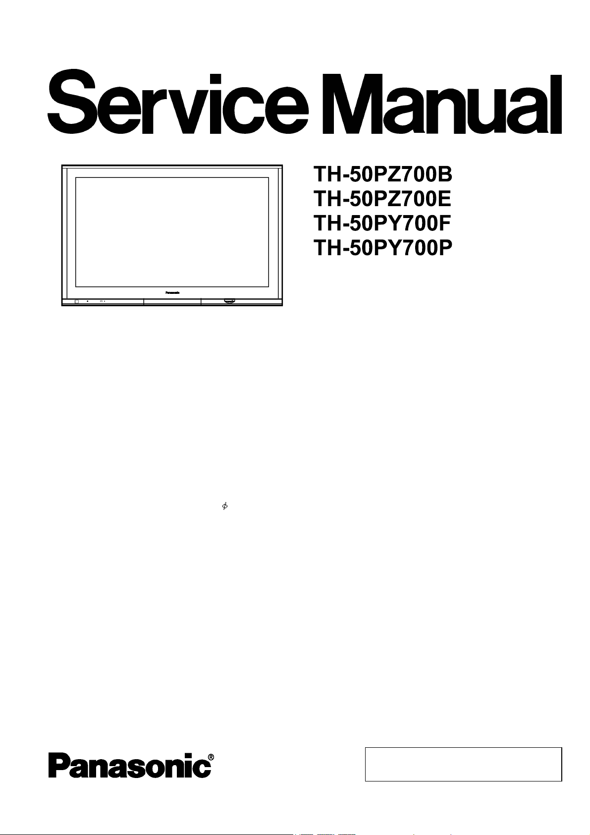
GPH10DE Chassis
A
V
r
K
ORDER NO. PCZ0705046CE
Plasma Television
Specifications
PowerSource
PowerConsumption
Average use 569 W
Standby condition 0.3 W (Wihe out DVB recording)
Displaypanel
Aspect Ratio 16 : 9
isible screen size 127 cm (diagonal)
Numberofpixels 2,073,600 (1,920 (W) × 1,080 (H)) [5,760 × 1,080 dots]
Sound
Speake
Audio Output 31 W (15.5 W + 15.5 W), 10 % THD
Headphones M3 (3.5 mm) stereo mini Jack × 1
PC signals VGA, SVGA, XGA
Receiving Systems/Band name PAL B, G, H, I, SECAM B, G, SECAML/L’
(Except B model) VHF E2 - E12 VHF H1 - H2 (ITALY)
C 220-240 V, 50/60 Hz
20 W (With DVB recording)
1,106 mm (W) × 622 mm (H)
Woofer( 80 mm) × 2 pcs, Tweeter (23 mm × 100 mm) × 2 pcs
SXGA ...... (compressed)
Horizontal scanning frequency31 - 69 kHz
Vertical scanning frequency59 - 86 Hz
VHF A - H (ITALY) UHF E21 - E69
CATV (S01 - S05) CATV S1 - S10 (M1 - M10)
CATV S11 - S20 (U1 - U10) CATV S21 - S41 (Hyperband)
PAL D, K, SECAMD,
VHF R1 - R2 VHF R3 - R5
VHF R6 - R12 UHF E21 - E69
PAL 525/60
Playback of NTSC tape from some PAL Video re cord ers (VCR)
© 2007 Matsushita Electric Industrial Co., Ltd. All
rights reserved. Unauthorized copying and
distribution is a violation of law.
r
r
4
A
Y
A
A
TH-50PZ700B / TH-50PZ700E / TH-50PY700F / TH-50PY70 0P
DVB (E model only)
Digital terrestrial services via VHF/UHF aerial input.
M.NTSC
Playback from M. NTSC Video recorders (VCR)
NTSC (AVinput only)
Playback from NTSC Video recorders (VCR)
lTV signals maynot be received in some areas.
Receiving Systems/Band name PAL I :UHF E21 - 68
(B model) PAL 525/60 :Playback of NTSC tape from some PAL Video recorders (VCR) o
NTSC disc playback from DVD playerand recorder.
DVB :Digital terrestrial services via UHF aerial input.
M.NTSC :Playback from M.NTSC Video recorders (VCR).
NTSC (AVinput only) :Playback from NTSC Video recorders (VCR).
Aerial - Rea
Operating Conditions Temperature: 0 °C - 35 °C
Connection Terminals
AV1 (Scart terminal) 21 Pin terminal (Audio/Video in, Audio/Video out, RGB in)
AV2 (Scart terminal) 21 Pin terminal (Audio/Video in, Audio/Video out, S-Video in, Q-Link)
AV3 (Scart terminal) 21 Pin terminal (Audio/Video in, Audio/Video out, RGB in, S-Video in, Q-Link)
AV
VIDEO RCA PIN Type × 1 1.0 V[p-p] (75 ohm)
S-VIDEO Mini DIN 4-pin Y:1.0 V[p-p] (75 ohm) C:0.286 V[p-p] (75 ohm)
UDIO L - R RCA PIN Type × 2 0.5 V[rms]
COMPONENTVIDEO
VIDEO
UDIO L - R RCA PIN Type × 2 0.5 V[rms]
Others
HDMI1 / 2 / 3 TYPE A Connectors lThis TV supports “HDAVI Control 2” function.
PC HIGH-DENSITY D-SUB 15PIN R,G,B/0.7 V[p-p] (75 ohm)
Card slot SD CARD slot × 1
Output
UDIO L - R RCA PIN Type × 2 0.5 V[rms] (high impedance)
DIGITAL AUDIO OUT PCM/DolbyDigital, Fiberoptic
Dimensions ( W × H × D ) 1,266 mm × 802 mm × 138 mm
Mass 48.0 kg Net
Note:
·
· Design and Specifications are subject to change without notice. Mass and Dimensions shown are approximate.
· ·
·
· This equipment complies with the EMC standards listed below.
· ·
EN55013, EN61000-3-2, EN61000-3-3, EN55020, EN55022, EN55024.
VHF/UHF (Except B model), UHF (B model)
Humidity: 20 % - 80 % RH (non-condensing)
1.0 V[p-p] (including synchronization)
PB,P
R
± 0.35 V [p-p]
HD, VD/TTL Level 2.0 - 5.0 V[p-p] (high impedance)
CONTENTS
Page Page
1 Applicable signals 5
2 Safety Precautions
2.1. General Guidelines
6
6
2.2. Touch-Current Check
3 Prevention of Electrostatic Discharge (ESD) to
Electrostatically Sensitive (ES) Devices
2
6
7
TH-50PZ700B / TH-50PZ700E / TH-50PY700F / TH-50PY70 0P
4 About lead free solder (PbF) 8
5 Service Hint
6 Plasma panel replacement method
6.1. Remove the Back cover
6.2. Remove the fan
6.3. Remove the rear terminal cover
6.4. Remove the P-Board
6.5. Remove the tuner unit
6.6. Remove the DH-Board
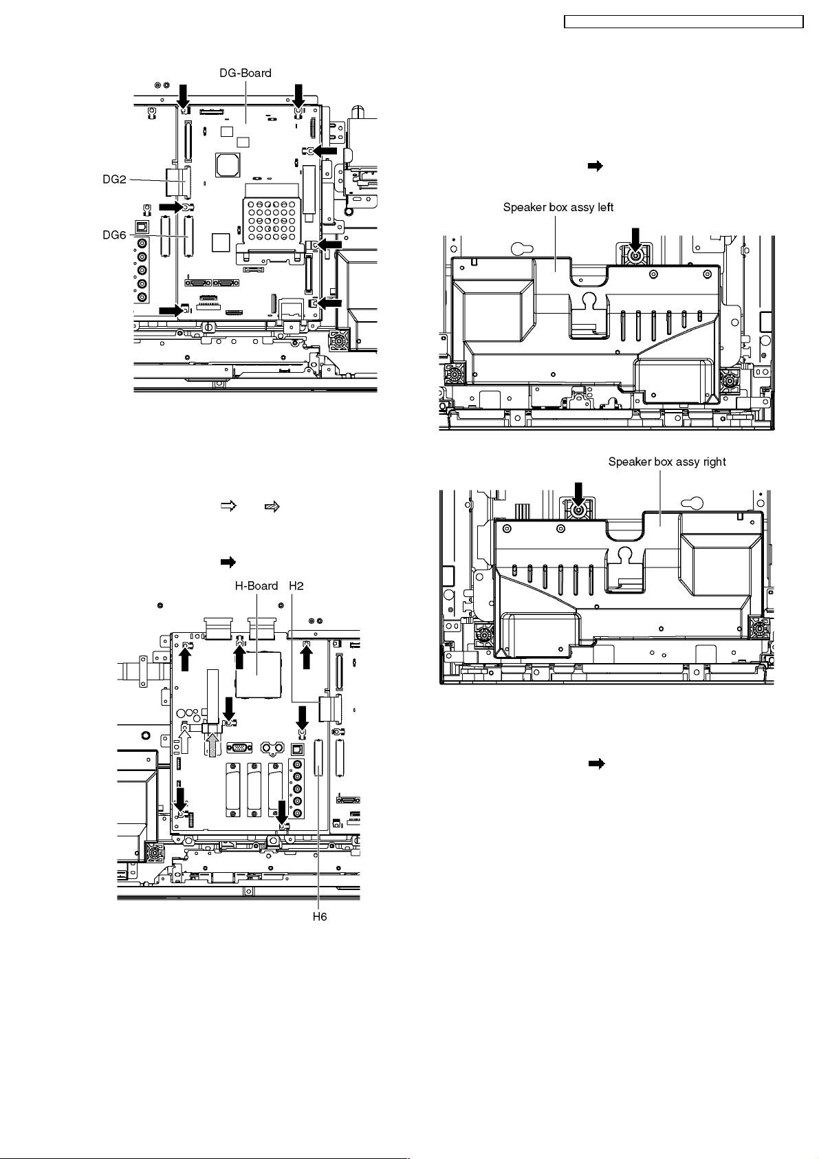
6.7. Remove the DG-Board
6.8. Remove the H-Board
6.9. Remove the speaker box assy (left, right)
6.10. Remove the JG-Board
6.11. Remove the PA-Board
6.12. Remove the D-Board
6.13. Remove the SU-Board
6.14. Remove the SD-Board
6.15. Remove the SC-Board
6.16. Remove the SS-Board
6.17. Remove the stand brackets
6.18. Remove the C1-Board
6.19. Remove the C2-Board
6.20. Remove the C3-Board
6.21. Remove the C4-Board
6.22. Remove the C5-Board
6.23. Remove the C6-Board
6.24. Remove the front bracket
6.25. Remove the G-Board and GH-Board
6.26. Remove the GS-Board
6.27. Remove the S-Board
6.28. Remove the K-Board
10
10
10
10
10
12
12
12
13
13
13
14
14
15
15
15
15
16
16
16
16
16
17
17
17
17
18
18
18
6.29. Remove the Plasma panel section from the Cabinet assy
(glass)
6.30. Remove the squawker speaker
6.31. Replace the plasma panel (finished)
7 Caution statement
7.1. Caution statement.
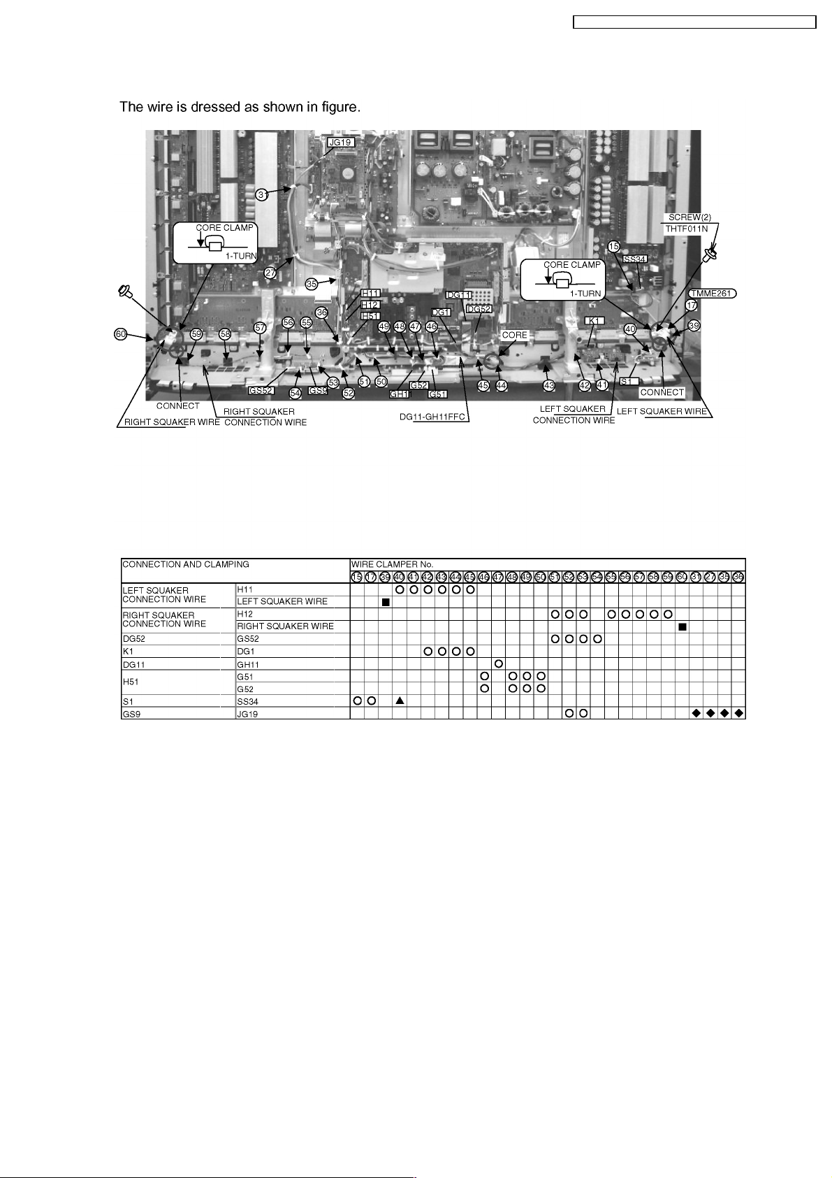
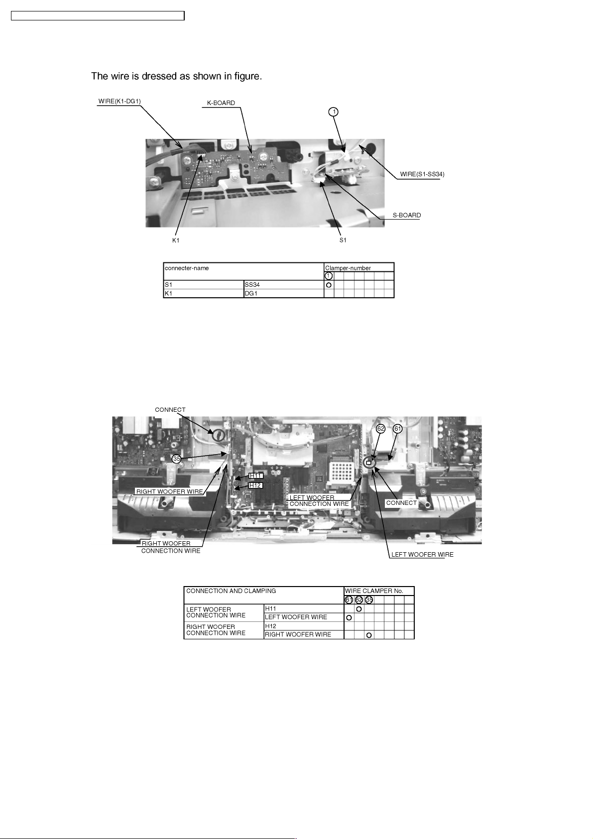
8 Location of Lead Wiring
8.1. Lead of Wiring (1)
8.2. Lead of Wiring (2)
8.3. Lead of Wiring (3)
9 Self-check Function
9.1. Check of the IIC bus lines
9.2. Power LED Blinking timing chart
9.3. No Power
9.4. No Picture
9.5. Local screen failure
10 Service Mode
10.1. How to enter into Service Mode
10.2. Service tool mode
11 Adjustment Procedure
11.1. Driver Set-up
11.2. Initialization Pulse Adjust
11.3. P.C.B. (Printed Circuit Board) exchange
18
19
20
21
21
22
22
23
24
25
25
26
27
28
29
30
30
32
33
33
34
34
11.4. Adjustment Volume Location
9
11.5. Test Point Location
12 Adjustment
12.1. Sub-Contrast adjustment
12.2. PAL panel white balance adjustment
12.3. HD white balance adjustment
13 Hotel mode
14 Conductor Views
14.1. P(MULTI)-Board
14.2. P(SUS)-Board
14.3. PA-Board
14.4. G-Board
14.5. H-Board
14.6. GH and GS-Board
14.7. JG-Board
14.8. DG-Board
14.9. DH-Board
14.10. D-Boa rd
14.11. C1-Bo ard
14.12. C2-Bo ard
14.13. C3-Bo ard
14.14. C4-Bo ard
14.15. C5-Bo ard
14.16. C6-Bo ard
14.17. SC-Bo ard
14.18. SU-Bo ard
14.19. SD-Bo ard
14.20. SS-Bo ard
14.21. K and S-Board
15 Schematic and Block Diagram
15.1. Schematic Diagram Note
15.2. Main Block Diagram
15.3. P-Board (1 of 2) Block Diagram
15.4. P-Board (2 of 2) Block Diagram
15.5. P-Board (1 of 2) Schematic Diagram
15.6. P-Board (2 of 2) Schematic Diagram
15.7. PA-Board Block Diagram
15.8. PA-Board (1 of 2) Schematic Diagram
15.9. PA-Board (2 of 2) Schematic Diagram
15.10. G and S-Board Schem atic Diagram
15.11. H-Boa rd (1 of 2) Block Diagram
15.12. H-Boa rd (2 of 2) Block Diagram
15.13. H-Boa rd (1 of 5) Schem atic Diagram
15.14. H-Boa rd (2 of 5) Schem atic Diagram
15.15. H-Boa rd (3 of 5) Schem atic Diagram
15.16. H-Boa rd (4 of 5) Schem atic Diagram
15.17. H-Boa rd (5 of 5) Schem atic Diagram
15.18. GH and K-Board Schematic Diagram
15.19. GS-B oard Block Diagra m
15.20. GS-B oard Schematic Diagram
15.21. JG-Bo ard Block Diagra m
15.22. JG-Bo ard (1 of 5) Schematic Diagram
15.23. JG-Bo ard (2 of 5) Schematic Diagram
15.24. JG-Bo ard (3 of 5) Schematic Diagram
35
35
36
36
37
38
39
41
41
44
47
48
49
51
52
54
57
58
60
61
62
63
64
65
66
69
70
71
74
75
75
76
77
78
79
80
81
82
83
84
85
86
87
88
89
90
91
92
93
94
95
96
97
98
3
TH-50PZ700B / TH-50PZ700E / TH-50PY700F / TH-50PY70 0P
15.25. JG-Bo ard (4 of 5) Schematic Diagram 99
15.26. JG-Bo ard (5 of 5) Schematic Diagram
15.27. DG-B oard (1 of 3) Block Diagram
15.28. DG-B oard (2 of 3) Block Diagram
15.29. DG-B oard (3 of 3) Block Diagram
15.30. DG-B oard (1 of 12) Schematic Diagram
15.31. DG-B oard (2 of 12) Schematic Diagram
15.32. DG-B oard (3 of 12) Schematic Diagram
15.33. DG-B oard (4 of 12) Schematic Diagram
15.34. DG-B oard (5 of 12) Schematic Diagram
15.35. DG-B oard (6 of 12) Schematic Diagram
15.36. DG-B oard (7 of 12) Schematic Diagram
15.37. DG-B oard (8 of 12) Schematic Diagram
15.38. DG-B oard (9 of 12) Schematic Diagram
15.39. DG-B oard (10 of 12) Schematic Diagram
15.40. DG-B oard (11 of 12) Schematic Diagram
15.41. DG-B oard (12 of 12) Schematic Diagram
15.42. DH-Board Block Diagram
15.43. DH-Board (1 of 4) Schematic Diagram
15.44. DH-Board (2 of 4) Schematic Diagram
15.45. DH-Board (3 of 4) Schematic Diagram
15.46. DH-Board (4 of 4) Schematic Diagram
15.47. D-Boa rd (1 of 2) Block Diagram
15.48. D-Boa rd (2 of 2) Block Diagram
15.49. D-Boa rd (1 of 8) Schem atic Diagram
15.50. D-Boa rd (2 of 8) Schem atic Diagram
15.51. D-Boa rd (3 of 8) Schem atic Diagram
15.52. D-Boa rd (4 of 8) Schem atic Diagram
15.53. D-Boa rd (5 of 8) Schem atic Diagram
15.54. D-Boa rd (6 of 8) Schem atic Diagram
15.55. D-Boa rd (7 of 8) Schem atic Diagram
15.56. D-Boa rd (8 of 8) Schem atic Diagram
15.57. C1, C2, C5 and C6 Block Diagram
100
101
102
103
104
105
106
107
108
109
110
111
112
113
114
115
116
117
118
119
120
121
122
123
124
125
126
127
128
129
130
131
15.58. C2, C3, C4 and C5-Board Block Diagram
15.59. C1-Bo ard (1 of 2) Schematic Diagram
15.60. C1-Bo ard (2 of 2) Schematic Diagram
15.61. C2-Bo ard (1 of 2) Schematic Diagram
15.62. C2-Bo ard (2 of 2) Schematic Diagram
15.63. C3-Bo ard (1 of 2) Schematic Diagram
15.64. C3-Bo ard (2 of 2) Schematic Diagram
15.65. C4-Bo ard (1 of 2) Schematic Diagram
15.66. C4-Bo ard (2 of 2) Schematic Diagram
15.67. C5-Bo ard (1 of 2) Schematic Diagram
15.68. C5-Bo ard (2 of 2) Schematic Diagram
15.69. C6-Bo ard (1 of 2) Schematic Diagram
15.70. C6-Bo ard (2 of 2) Schematic Diagram
15.71. SC-Bo ard Block Diagra m
15.72. SC-Bo ard (1 of 2) Schematic Diagram
15.73. SC-Bo ard (2 of 2) Schematic Diagram
15.74. SU and SD-Board Block Diagram
15.75. SU-Bo ard (1 of 3) Schematic Diagram
15.76. SU-Bo ard (2 of 3) Schematic Diagram
15.77. SU-Bo ard (3 of 3) Schematic Diagram
15.78. SD-Bo ard (1 of 3) Schematic Diagram
15.79. SD-Bo ard (2 of 3) Schematic Diagram
15.80. SD-Bo ard (3 of 3) Schematic Diagram
15.81. SS-Bo ard Block Diagra m
15.82. SS-Bo ard Schematic Diagram
16 Exploded Views & Replacement Parts List
16.1. Exploded Views
16.2. Packing Exploded Views (1)
16.3. Packing Exploded Views (2)
16.4. Packing Exploded Views (3)
16.5. Replacement Parts List Notes
16.6. Mechanical Replacement Parts List
16.7. Electrical Replacement Parts List
132
133
134
135
136
137
138
139
140
141
142
143
144
145
146
147
148
149
150
151
152
153
154
155
156
157
157
158
159
160
161
162
164
4
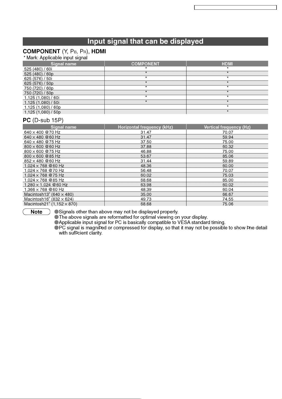
1 Applicable signals
TH-50PZ700B / TH-50PZ700E / TH-50PY700F / TH-50PY70 0P
5
TH-50PZ700B / TH-50PZ700E / TH-50PY700F / TH-50PY70 0P
2 Safety Precautions
2.1. General Guidelines
1. When conducting repairs and servicing, do not attempt to modify the equipment, its parts or its materials.
2. When wiring units (with cables, flexible cables or lead wires) are supplied as repair parts and only one wire or some of the wires
have been broken or disconnected, do not attempt to repair or re-wire the units. Replace the entire wiring unit instead.
3. When conducting repairs and servicing, do not twist the Faston connectors but plug them straight in or unplug them straight out.
4. When servicing, observe the original lead dress. If a short circuit is found, replace all parts which have been overheated or
damaged by the short circuit.
5. After servicing, see to it that all the protective devices such as insulation barriers, insulation papers shields are properly
installed.
6. After servicing, make the following leakage current checks to prevent the customer from being exposed to shock hazards.
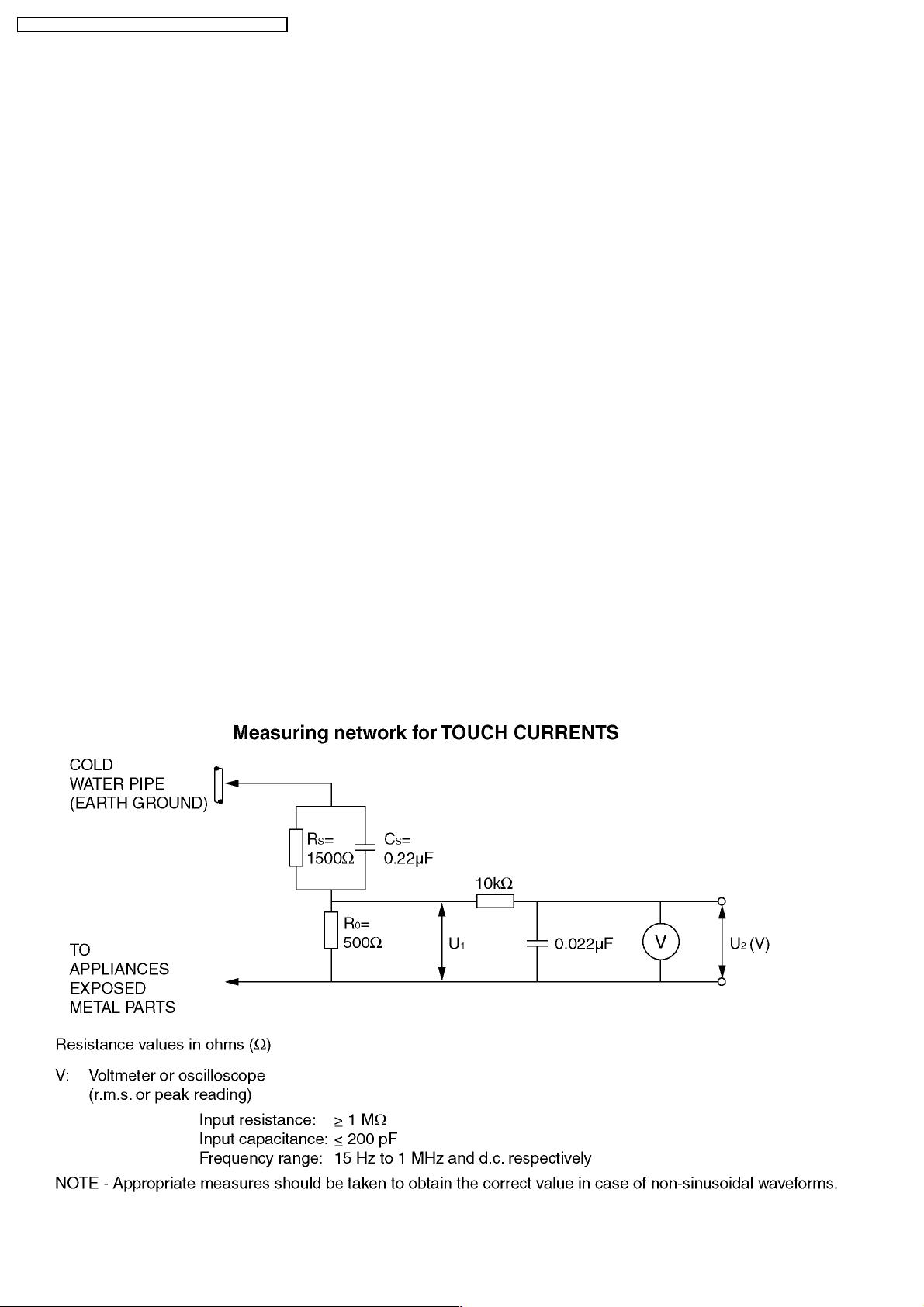
2.2. Touch-Current Check
1. Plug the AC cord directly into the AC outlet. Do not use an isolation transformer for this check.
2. Connect a measuring network for touch currents between each exposed metallic part on the set and a good earth ground such
as a water pipe, as shown in Figure 1.
3. Use Leakage Current Tester (Simpson 228 or equivalent) to measure the potential across the measuring network.
4. Check each exposed metallic part, and measure the voltage at each point.
5. Reserve the AC plug in the AC outlet and repeat each of the above measure.
6. The potential at any point (TOUGH CURRENT) expressed as voltage U
For a. c.: U
For d. c.: U
= 35 V (peak) and U2= 0.35 V (peak);
1
= 1.0 V,
1
Note:
The limit value of U
= 0.35 V (peak) for a. c. and U1= 1.0 V for d. c. correspond to the values 0.7 mA (peak) a. c. and 2.0
2
mA d. c.
The limit value U
= 35 V (peak) for a. c. correspond to the value 70 mA (peak) a. c. for frequencies greater than 100 kHz.
1
7. In case a measurement is out of the limits specified, there is a possibility of a shock hazard, and the equipment should be
repaired and rechecked before it is returned to the customer.
and U2, does not exceed the following values:
1
Figure 1
6
TH-50PZ700B / TH-50PZ700E / TH-50PY700F / TH-50PY70 0P
3 Prevention of Electrostatic Discharge (ESD) to
Electrostatically Sensitive (ES) Devices
Some semiconductor (solid state) devices can be damaged easily by static electricity. Such components commonly are called
Electrostatically Sensitive (ES) Devices. Examples of typical ES devices are integrated circuits and some field-effect transistors and
semiconductor "chip" components. The following techniques should be used to help reduce the incidence of component damage
caused by electrostatic discharge (ESD).
1. Immediately before handling any semiconductor component or semiconductor-equipped assembly, drain off any ESD on your
body by touching a known earth ground. Alternatively, obtain and wear a commercially available discharging ESD wrist strap,
which should be removed for potential shock reasons prior to applying power to the unit under test.
2. After removing an electrical assembly equipped with ES devices, place the assembly on a conductive surface such as
aluminum foil, to prevent electrostatic charge buildup or exposure of the assembly.
3. Use only a grounded-tip soldering iron to solder or unsolder ES devices.
4. Use only an anti-static solder removal device. Some solder removal devices not classified as "anti-static (ESD protected)" can
generate electrical charge sufficient to damage ES devices.
5. Do not use freon-propelled chemicals. These can generate electrical charges sufficient to damage ES devices.
6. Do not remove a replacement ES device from its protective package until immediately before you are ready to install it. (Most
replacement ES devices are packaged with leads electrically shorted together by conductive foam, aluminum foil or comparable
conductive material).
7. Immediately before removing the protective material from the leads of a replacement ES device, touch the protective material
to the chassis or circuit assembly into which the device will be installed.
Caution
Be sure no power is applied to the chassis or circuit, and observe all other safety precautions.
8. Minimize bodily motions when handling unpackaged replacement ES devices. (Otherwise ham less motion such as the brushing
together of your clothes fabric or the lifting of your foot from a carpeted floor can generate static electricity (ESD) sufficient to
damage an ES device).
7
TH-50PZ700B / TH-50PZ700E / TH-50PY700F / TH-50PY70 0P
4 About lead free solder (PbF)
Note: Lead is listed as (Pb) in the periodic table of elements.
In the information below, Pb will refer to Lead solder, and PbF will refer to Lead Free Solder.
The Lead Free Solder used in our manufacturing process and discussed below is (Sn+Ag+Cu).
That is Tin (Sn), Silver (Ag) and Copper (Cu) although other types are available.
This model uses Pb Free solder in it’s manufacture due to environmental conservation issues. For service and repair work, we’d
suggest the use of Pb free solder as well, although Pb solder may be used.
PCBs manufactured using lead free solder will have the PbF within a leaf Symbol PbF stamped on the back of PCB.
Caution
·
· Pb free solder has a higher melting point than standard solder. Typically the melting point is 50 ~ 70 °F (30~40 °C) higher.
· ·
Please use a high temperature soldering iron and set it to 700 ± 20 °F (370 ± 10 °C).
·
· Pb free solder will tend to splash when heated too high (about 1100 °F or 600 °C).
· ·
If you must use Pb solder, please completely remove all of the Pb free solder on the pins or solder area before applying Pb
solder. If this is not practical, be sure to heat the Pb free solder until it melts, before applying Pb solder.
·
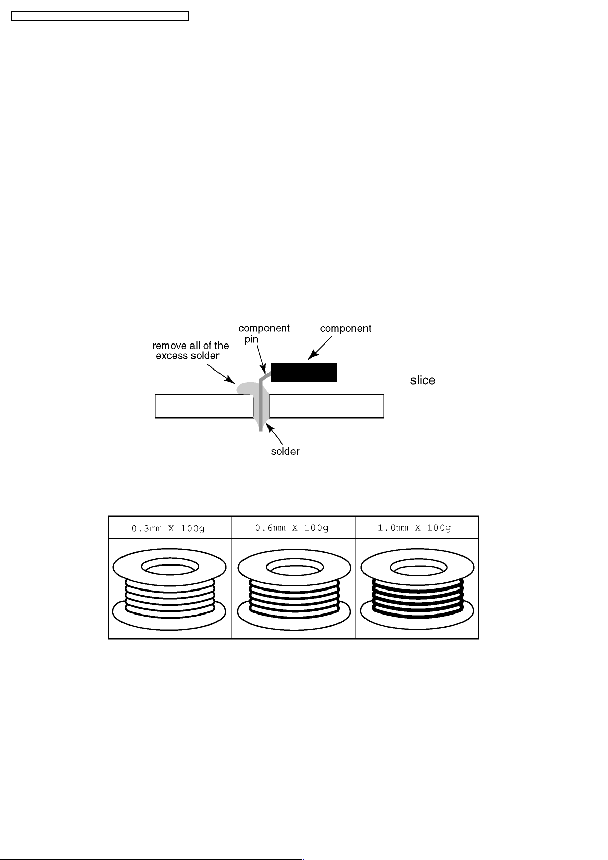
· After applying PbF solder to double layered boards, please check the component side for excess solder which may flow onto
· ·
the opposite side. (see figure below)
Suggested Pb free solder
There are several kinds of Pb free solder available for purchase. This product uses Sn+Ag+Cu (tin, silver, copper) solder.
However, Sn+Cu (tin, copper), Sn+Zn+Bi (tin, zinc, bismuth) solder can also be used.
8
5 Service Hint
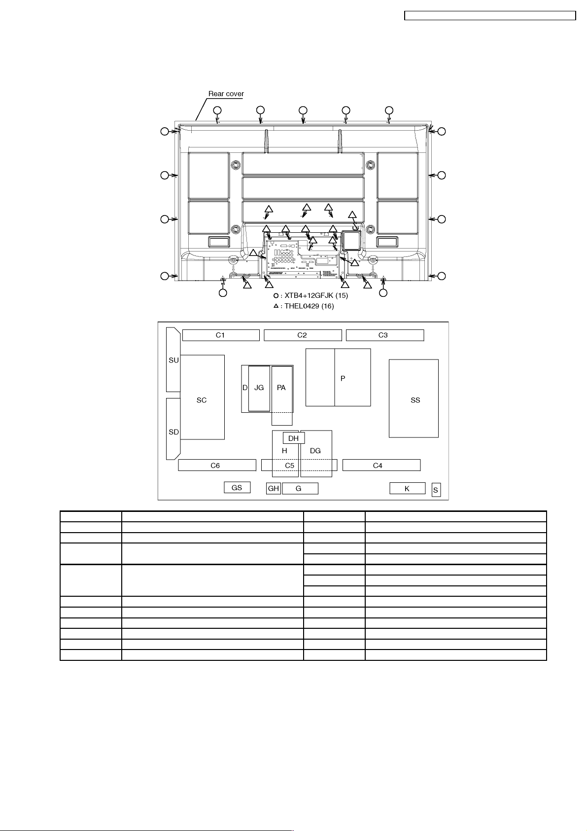
Remove the Rear Cover
TH-50PZ700B / TH-50PZ700E / TH-50PY700F / TH-50PY70 0P
Board Name Function Board Name Function
P Power Supply D Format Converter, Plasma AI, Sub-Field Processor
PA Fan control, DC-DC converter C1 Data Driver (Upper Right)
H Speaker out, Sound Processor
AV Terminal, AV Switch
DG DC-DC Converter
Digital Signal Processor, Microcomputer
HDMI Interface, Peaks Lite 2
DH Full HD SC Scan Drive
G Front terminal, Key Switch SU Scan out (Upper)
K Remote receiver, Power LED SD Scan out (Lower)
S Power Switch SS Sustain Drive
GS SD Card Slot JG H264 Decorder
GH HDMI3 terminal
C2 Data Driver (Upper Center)
C3 Data Driver (Upper Left)
C4 Data Driver (Lower Left)
C5 Data Driver (Lower Center)
C6 Data Driver (Lower Right)
9
TH-50PZ700B / TH-50PZ700E / TH-50PY700F / TH-50PY70 0P
6 Plasma panel replacement method
6.1. Remove the Back cover
1. See Service Hint. (Section 5)
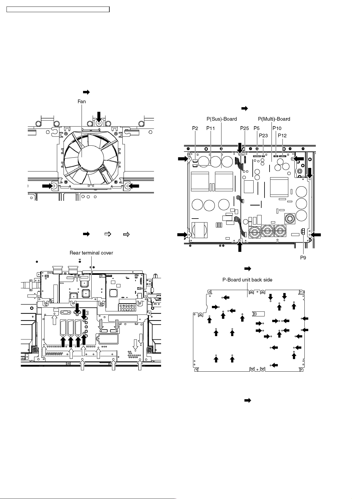
6.2. Remove the fan
1. Disconnect the relay connectors.
2. Remove the screws (×3
each) and remove the fan.
6.3. Remove the rear terminal
cover
6.4. Remove the P-Board
Caution:
To remove P.C.B. wait 1 minute after power was off for
discharge from electrolysis capacitors.
1. Unlock the cable clampers to free the cable.
2. Disconnect the connectors (P2, P5, P9, P10, P11, P12, P23
and P25).
3. Remove the screws (×7
) and remove the P-Board unit.
1. Remove the screws (×6 , ×12 ,×2 ).
2. Remove the rear terminal cover.
4. Remove the screws (×28 ) on the back side.
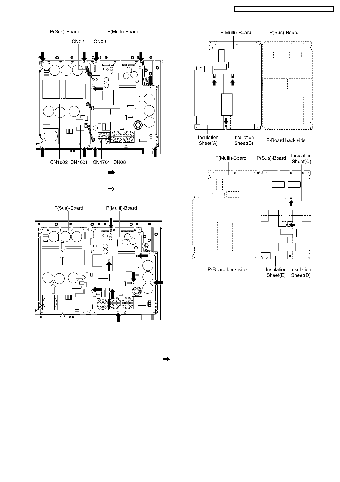
5. Disconnect the connectors (CN06-CN02, CN08-CN1602
and CN1702-CN1601).
6. Remove the screws (×10
).
10
7. Remove the molding props (×8 ).
8. Remove the P(Multi)-Board.
9. Remove the molding props (×5
10. Remove the P(Sus)-Board.
TH-50PZ700B / TH-50PZ700E / TH-50PY700F / TH-50PY70 0P
).
Note:
When assembling the P(Multi)-Board and the P(Sus)Board, the position of each hole of the insulation sheets(A,
B, C, D, E) is set to the position of each hole of the P(Multi)Board and the P(Sus)-Board and then assemble them. (
marks indicate setting positions.)
11
TH-50PZ700B / TH-50PZ700E / TH-50PY700F / TH-50PY70 0P
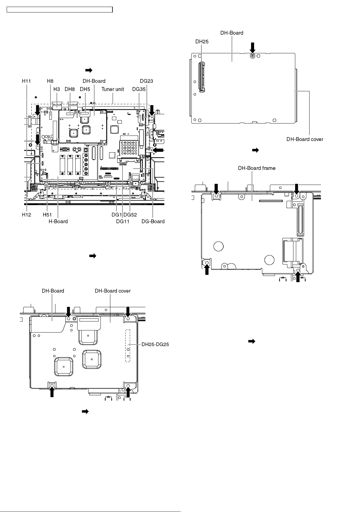
6.5. Remove the tuner unit
1. Unlock the cable clampers to free the cable.
2. Disconnect the connectors (DG1, DG11, DG23, DG35,
DG52, DH5, DH8, H3, H8, H11, H12 and H51).
3. Remove the screws (×4
) and remove the tuner unit.
4. Remove the screws (×4 ) and remove the DH-Board
frame.
6.6. Remove the DH-Board
1. Remove the tuner unit. (See section 6.5.)
2. Remove the screws (×4
cover and DH-Board.
(Be careful the connector (DH25-DG25) when remove the
DH-Board.)
3. Remove the screw (×1 ) and remove the DH-Board from
DH-Board cover.
) and remove the DH-Board
6.7. Remove the DG-Board
1. Remove the tuner unit. (See section 6.5.)
2. Remove the DH-Board and the DH-Board frame. (See
section 6.6.)
3. Disconnect the connector (DG2 and DG6).
4. Remove the screws (×7 ) and remove the DG-Board.
12
TH-50PZ700B / TH-50PZ700E / TH-50PY700F / TH-50PY70 0P
6.9. Remove the speaker box assy
(left, right)
1. Unlock the cable clampers to free the cable.
2. Disconnect the relay connectors.
3. Remove the screw (×1
assy (left, right).
) and remove the speaker box
6.8. Remove the H-Board
1. Remove the tuner unit. (See section 6.5.)
2. Remove the DH-Board and the DH-Board frame. (See
section 6.6.)
3. Remove the screws (×1
fixing metal.
4. Disconnect the connector (H2 and H6).
5. Remove the screws (×7
,×1 ) and remove the tuner
) and remove the H-Board.
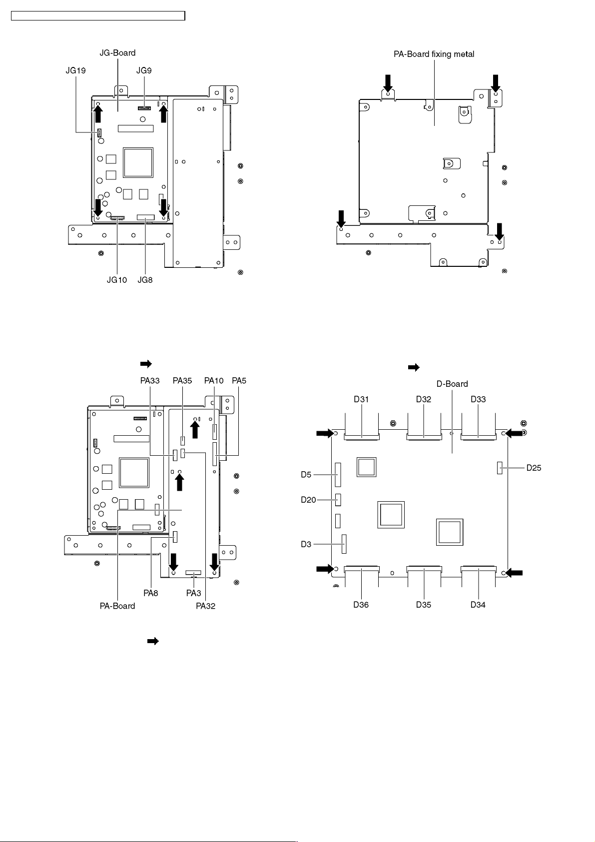
6.10. Remove the JG-Board
1. Disconnect the connector (JG8, JG9, JG10 and JG19).
2. Remove the screws (×4
) and remove the JG-Board.
13
TH-50PZ700B / TH-50PZ700E / TH-50PY700F / TH-50PY70 0P
6.11. Remove the PA-Board
1. Unlock the cable clampers to free the cable.
2. Disconnect the connectors (PA3, PA5, PA10, PA32, PA33
and PA35).
3. Remove the screws (×4
) and remove the PB-Board.
6.12. Remove the D-Board
1. Remove the PA-Board fixing metal. (See section 6.11.)
2. Disconnect the connectors (D3, D5, D20 and D25).
3. Disconnect the flexible cables (D31, D32, D33, D34, D35
and D36).
4. Remove the screws (×4 ) and remove the D-Board.
4. Remove the JG-Board. (See section 6.10.)
5. Remove the screws (×4
fixing metal.
) and remove the PA-Board
14
TH-50PZ700B / TH-50PZ700E / TH-50PY700F / TH-50PY70 0P
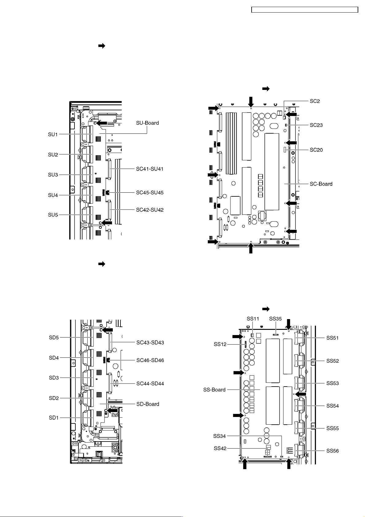
6.13. Remove the SU-Board
1. Remove the screws (×2 ).
2. Remove the flexible cables (SU1, SU2, SU3, SU4 and SU5)
connected to the SU-Board and remove the connectors
(SC45-SU45).
3. Slide the SU-Board to the left to disconnect from
connectors (SC41-SU41 and SC42-SU42) on the SC-Board
and remove the SU-Board.
6.15. Remove the SC-Board
1. Unlock the cable clampers to free the cable.
2. Remove the SU-Board and SD-Board. (See section 6.13.
and 6.14.)
3. Unlock the cable clampers to free the cable.
4. Disconnect the connectors (SC2, SC20 and SC23).
5. Remove the screws (×9
) and remove the SC-Board.
6.14. Remove the SD-Board
1. Remove the screws (×2 ).
2. Remove the flexible cables (SD1, SD2, SD3, SD4 and SD5)
connected to the SD-Board and remove the connector
(SC46-SD46).
3. Slide the SD-Board to the left to disconnect from
connectors (SC43-SD43 and SC44-SD44) on the SC-Board
and remove the SD-Board.
6.16. Remove the SS-Board
1. Disconnect the connectors (SS11, SS12, SS35, SS42 and
SS44).
2. Disconnect the flexible cables (SS51, SS52, SS53, SS54,
SS55 and SS56).
3. Remove the screws (×7
) and remove the SS-Board.
15
TH-50PZ700B / TH-50PZ700E / TH-50PY700F / TH-50PY70 0P
6.17. Remove the stand brackets
1. Remove the plasma panel section from the servicing stand
and lay on a flat surface such as a table (covered) with the
plasma panel surface facing downward.
2. Remove the stand brackets (left, right) fastening screws (×5
each) and remove the stand brackets (left, right).
6.20. Remove the C3-Board
1. Remove the fans. (See section 6.2.)
2. Remove the flexible cables holder fastening screws (×10
).
3. Disconnect the flexible cables (CA11, CA12, CA13, CA14
and CA15).
4. Disconnect the flexible cable (C31).
5. Disconnect the connector (C35).
6. Remove the screws (×5
) and remove the C3-Board.
6.18. Remove the C1-Board
1. Remove the fans. (See section 6.2.)
2. Remove the flexible cables holder fastening screws (×10
).
3. Disconnect the flexible cables (CA1, CA2, CA3, CA4, and
CA5).
4. Disconnect the flexible cables (C10 and C11).
5. Remove the screws (×5
) and remove the C1-Board.
6.19. Remove the C2-Board
1. Remove the fans. (See section 6.2.)
2. Remove the flexible cables holder fastening screws (×10
).
3. Disconnect the flexible cables (CA6, CA7, CA8, CA9 and
CA10).
4. Disconnect the flexible cables (C21, C22, C24 and C25).
5. Remove the screws (×5 ) and remove the C2-Board.
6.21. Remove the C4-Board
1. Remove the speaker box assy left. (See section 6.9.)
2. Remove the stand bracket left. (See section 6.17.)
3. Remove the flexible cables holder fastening screws (×10
).
4. Disconnect the flexible cables (CB11, CB12, CB13, CB14
and CB15).
5. Disconnect the flexible cable (C41).
6. Disconnect the connectors (C42 and C44).
7. Remove the screws (×5
) and remove the C4-Board.
16
TH-50PZ700B / TH-50PZ700E / TH-50PY700F / TH-50PY70 0P
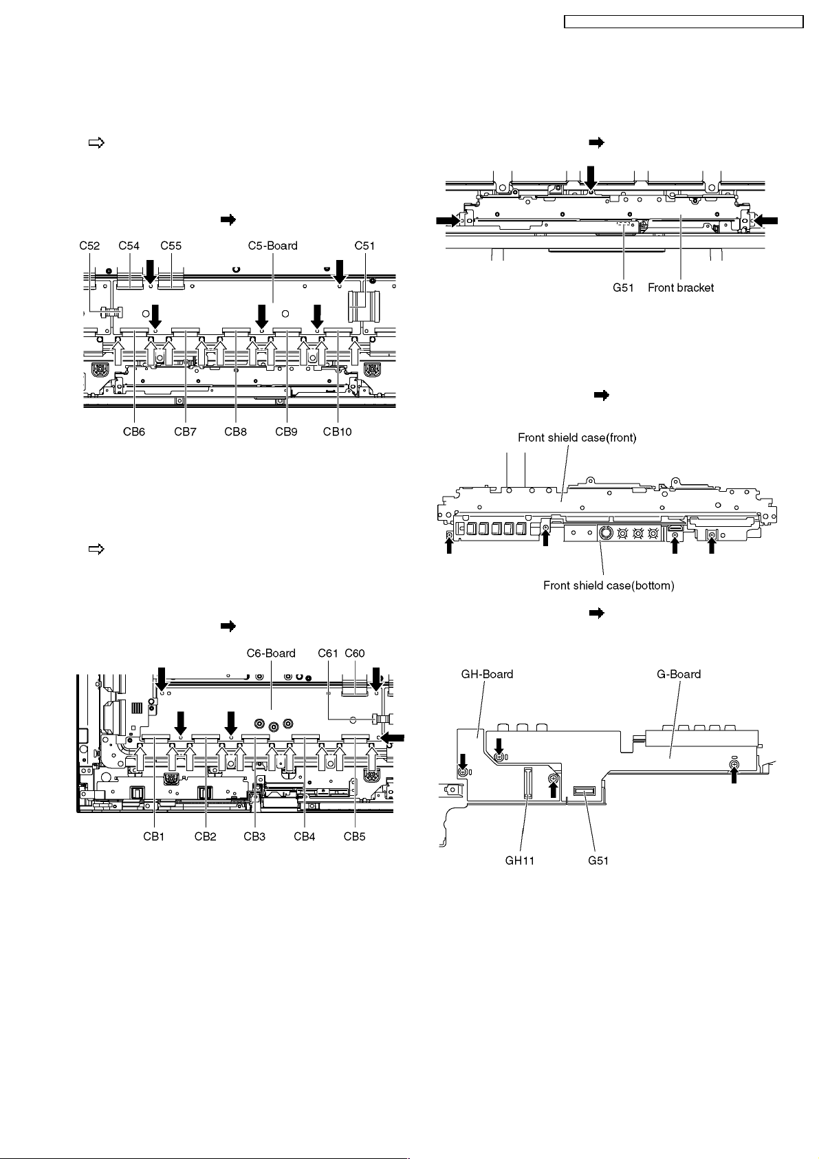
6.22. Remove the C5-Board
1. Remove the tuner unit. (See section 6.5.)
2. Remove the flexible cables holder fastening screws (×10
).
3. Disconnect the flexible cables (CB6, CB7, CB8, CB9 and
CB10).
4. Disconnect the flexible cables (C51, C52, C54 and C55).
5. Remove the screws (×5 ) and remove the C5-Board.
6.23. Remove the C6-Board
6.24. Remove the front bracket
1. Unlock the cable clampers to free the cable.
2. Disconnect the connector (G51).
3. Remove the screws (×3
) and remove the front bracket.
6.25. Remove the G-Board and GHBoard
1. Remove the front bracket. (See section 6.24.)
2. Remove the screws (×4
case (front).
) and remove the front shield
1. Remove the speaker box assy right. (See section 6.9.)
2. Remove the stand bracket right. (See section 6.17.)
3. Remove the flexible cables holder fastening screws (×10
).
4. Disconnect the flexible cables (CB1, CB2, CB3, CB4 and
CB5).
5. Disconnect the flexible cables (C60 and C61).
6. Remove the screws (×5
) and remove the C6-Board.
3. Remove the screws (×4 ) and disconnect the connector
(G51 and GH11).
4. Remove the G-Board and GH-Board.
17
TH-50PZ700B / TH-50PZ700E / TH-50PY700F / TH-50PY70 0P
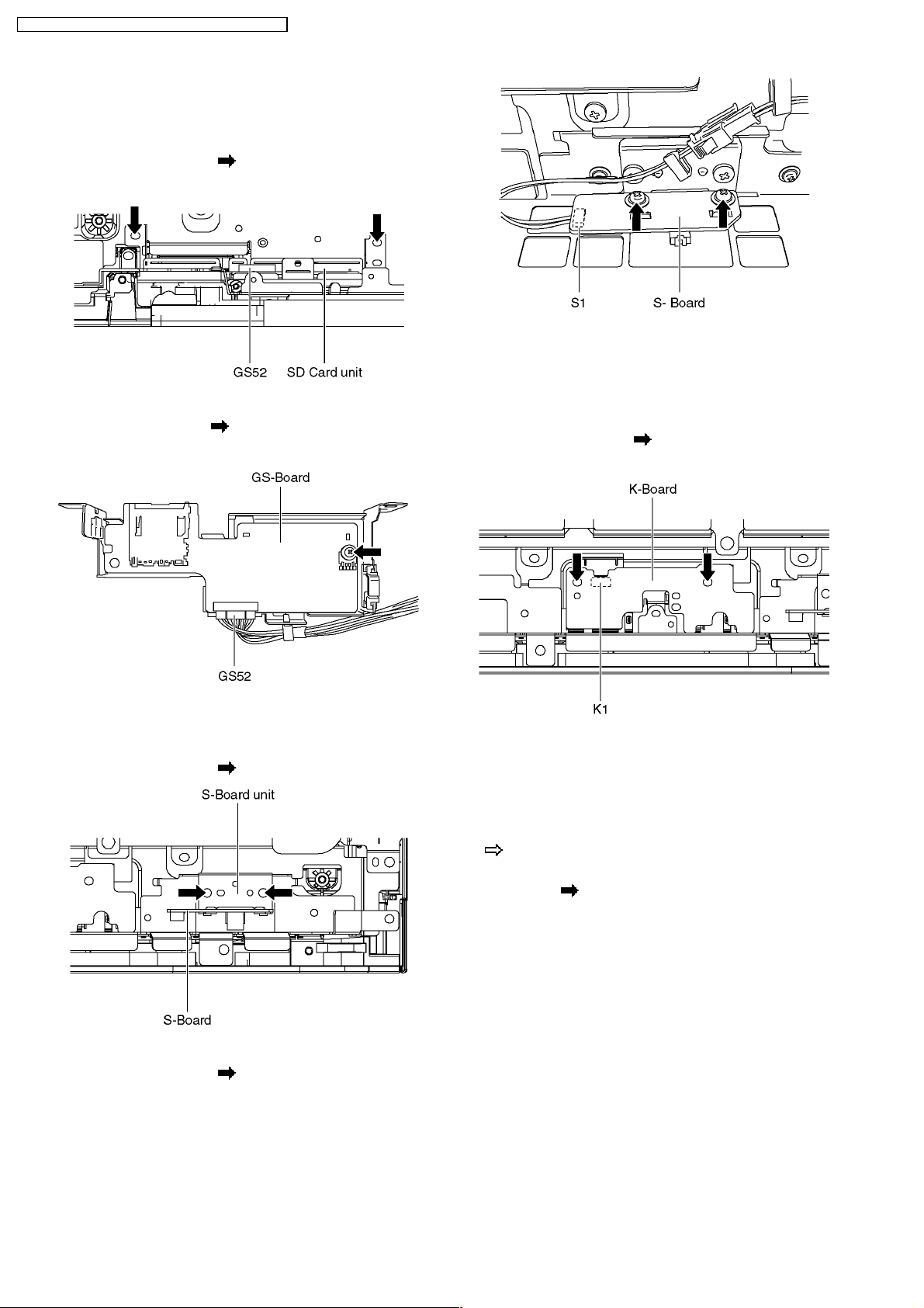
6.26. Remove the GS-Board
1. Remove the stand bracket right. (See section 6.17.)
2. Unlock the cable clampers to free the cable.
3. Remove the screws (×2
4. Remove the SD card unit.
5. Disconnect the connector (GS52).
6. Remove the screw (×1
7. Remove the GS-Board.
).
).
6.28. Remove the K-Board
1. Remove the speaker box assy left. (See section 6.9.)
2. Remove the S-Board. (See section 6.27.)
3. Unlock the cable clampers to free the cable.
4. Remove the screws (×2
5. Disconnect the connectors (K1) and remove the K-Board.
).
6.27. Remove the S-Board
1. Remove the speaker box assy left. (See section 6.9.)
2. Remove the screws (×2
3. Disconnect the connector (S1).
4. Remove the screws (×2
) and remove the S-Board unit.
) and remove the S-Board.
6.29. Remove the Plasma panel
section from the Cabinet assy
(glass)
1. Remove the stand brackets (left, right) fastening screw (×1
each).
2. Remove the cabinet assy and the plasma panel fastening
screws (×13
).
18
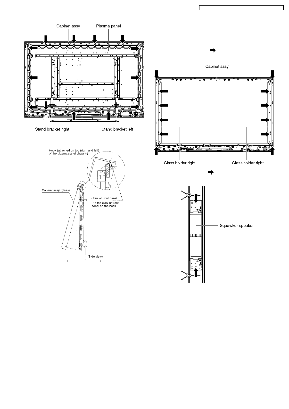
3. For leaving the plasma panel from the cabinet assy, pull the
bottom of the front frame forward, lift, and remove.
TH-50PZ700B / TH-50PZ700E / TH-50PY700F / TH-50PY70 0P
6.30. Remove the squawker speaker
1. Remove the cabinet assy. (See section 6.29.)
2. Disconnect the relay connectors.
3. Remove the screws (×12
4. Remove the glass holders (left, right).
).
5. Remove the screws (×2 ).
6. Remove the squawker speaker.
19

TH-50PZ700B / TH-50PZ700E / TH-50PY700F / TH-50PY70 0P
6.31. Replace the plasma panel
(finished)
1. Place the new plasma panel (finished) on the flat surface of
the table (covered by a soft cloth), with the plasma panel
surface facing downward.
2. Attach the C1, C2, C3,C4,C5-Board and the C6-Board,
connect the flexible cables (×30) from the Plasma panel to
the C1, C2, C3,C4,C5-Board and the C6-Board, and fit the
flexible cable holders.
3. Attach the Hooks (left, right) and fit the Reinforcement
Angles (L, R) and the Connection Plate (A, B, C, D) to the
new plasma panel.
4. Place the plasma panel section on the servicing stand.
5. Attach the cabinet assy and each P.C.Board and so on, to
the new plasma panel.
* When fitting the cabinet assy, be careful not to allow
any debris, dust or handling residue to remain between
the front glass and plasma panel.
20

7 Caution statement
7.1. Caution statement.
Caution:
Please confirm that all flexible cables are assembled correctly.
Also make sure that they are locked in the connectors.
Verify by giving the flexible cables a very slight pull.
TH-50PZ700B / TH-50PZ700E / TH-50PY700F / TH-50PY70 0P
21
TH-50PZ700B / TH-50PZ700E / TH-50PY700F / TH-50PY70 0P
8 Location of Lead Wiring
8.1. Lead of Wiring (1)
22
8.2. Lead of Wiring (2)
TH-50PZ700B / TH-50PZ700E / TH-50PY700F / TH-50PY70 0P
23
TH-50PZ700B / TH-50PZ700E / TH-50PY700F / TH-50PY70 0P
8.3. Lead of Wiring (3)
24
TH-50PZ700B / TH-50PZ700E / TH-50PY700F / TH-50PY70 0P
9 Self-check Function
Use the self-check function to test the unit.
1. Checking the IIC bus lines
2. Power LED Blinking timing
9.1. Check of the IIC bus lines
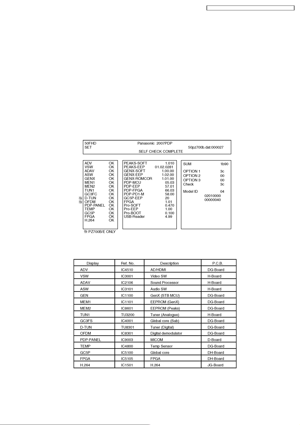
9.1.1. How to access
Self-check indication only:
Produce TV reception screen, and while pressing [VOLUME ( - )] button on the main unit, press [OK] button on the remote control
for more than 3 seconds.
Self-check indication and forced to factory shipment setting:
Produce TV reception screen, and while pressing [VOLUME ( - )] button on the main unit, press [MENU] button on the remote
control for more than 3 seconds.
9.1.2. Screen display
9.1.3. Check Point
Confirm the following parts if NG was displayed.
9.1.4. Exit
Disconnect the AC cord from wall outlet.
25
TH-50PZ700B / TH-50PZ700E / TH-50PY700F / TH-50PY70 0P
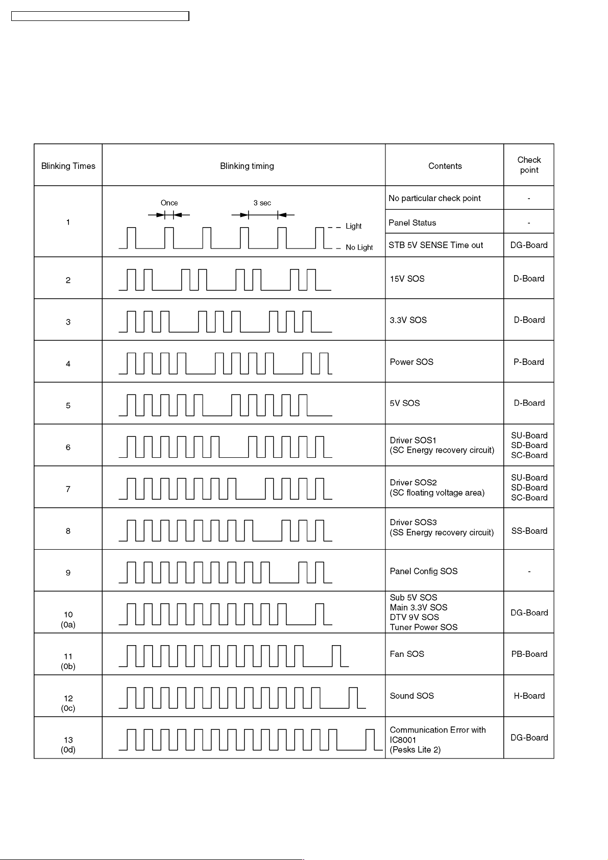
9.2. Power LED Blinking timing chart
1. Subject
Information of LED Flashing timing chart.
2. Contents
When an abnormality has occurred the unit, the protection circuit operates and reset to the stand by mode. At this time, the
defective block can be identified by the number of blinks of the Power LED on the front panel of the unit.
26
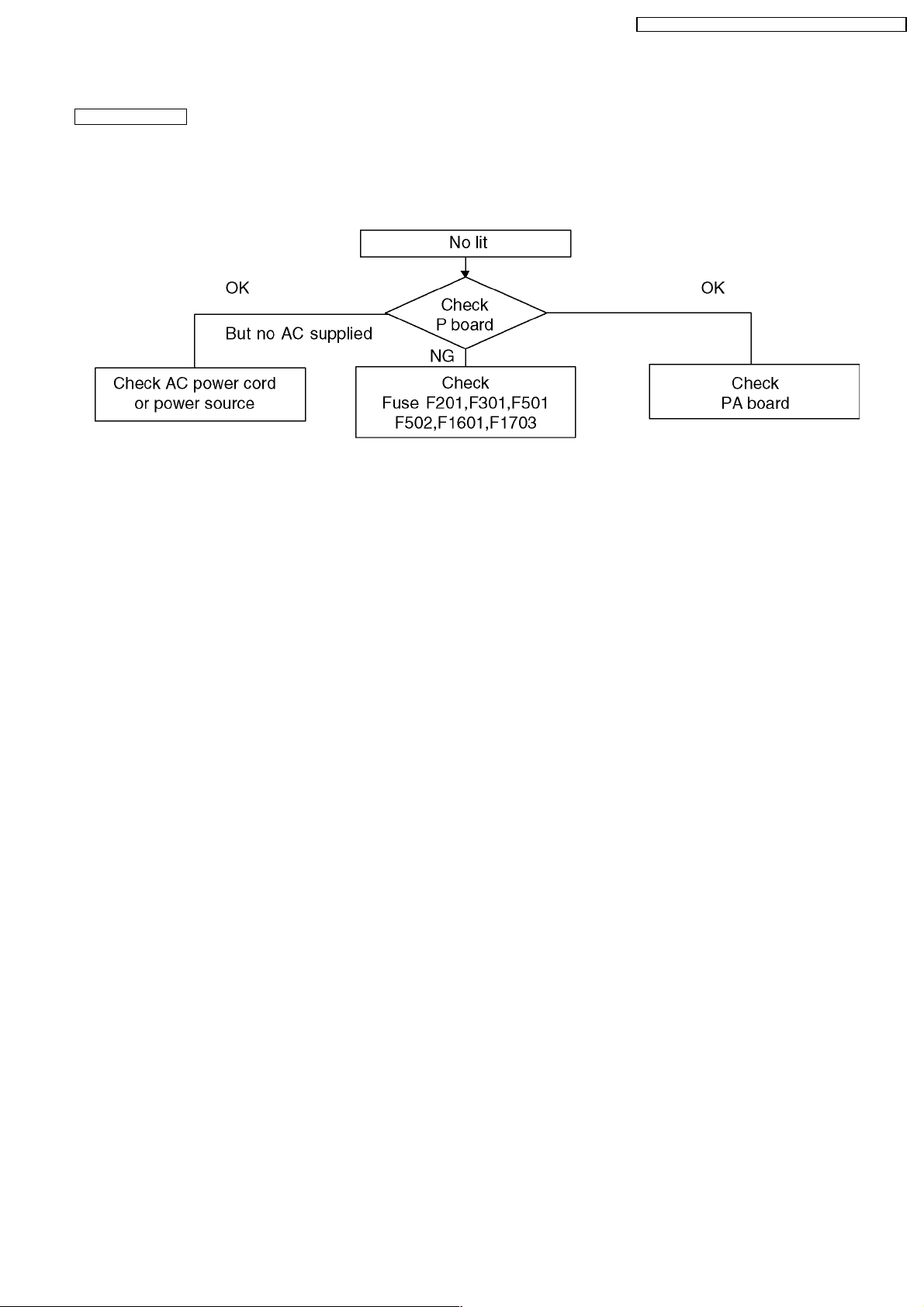
9.3. No Power
First check point
There are following 2 states of No Power indication by power LED.
1. No lit
2. Red is lit then turns red blinking a few seconds later. (See 9.2.)
TH-50PZ700B / TH-50PZ700E / TH-50PY700F / TH-50PY70 0P
27
TH-50PZ700B / TH-50PZ700E / TH-50PY700F / TH-50PY70 0P
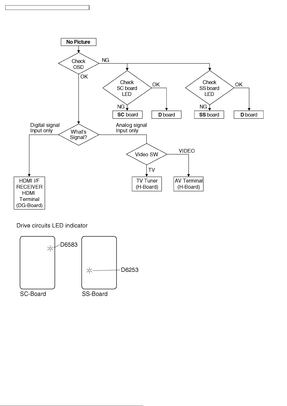
9.4. No Picture
28
TH-50PZ700B / TH-50PZ700E / TH-50PY700F / TH-50PY70 0P
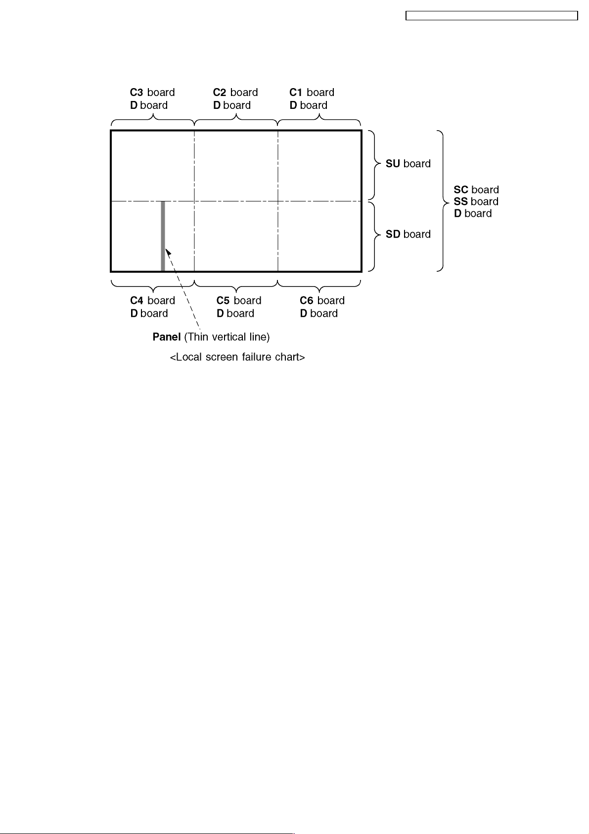
9.5. Local screen failure
Plasma display may have local area failure on the screen. Fig-1 is the possible defect P.C.B. for each local area.
Fig-1
29
TH-50PZ700B / TH-50PZ700E / TH-50PY700F / TH-50PY70 0P
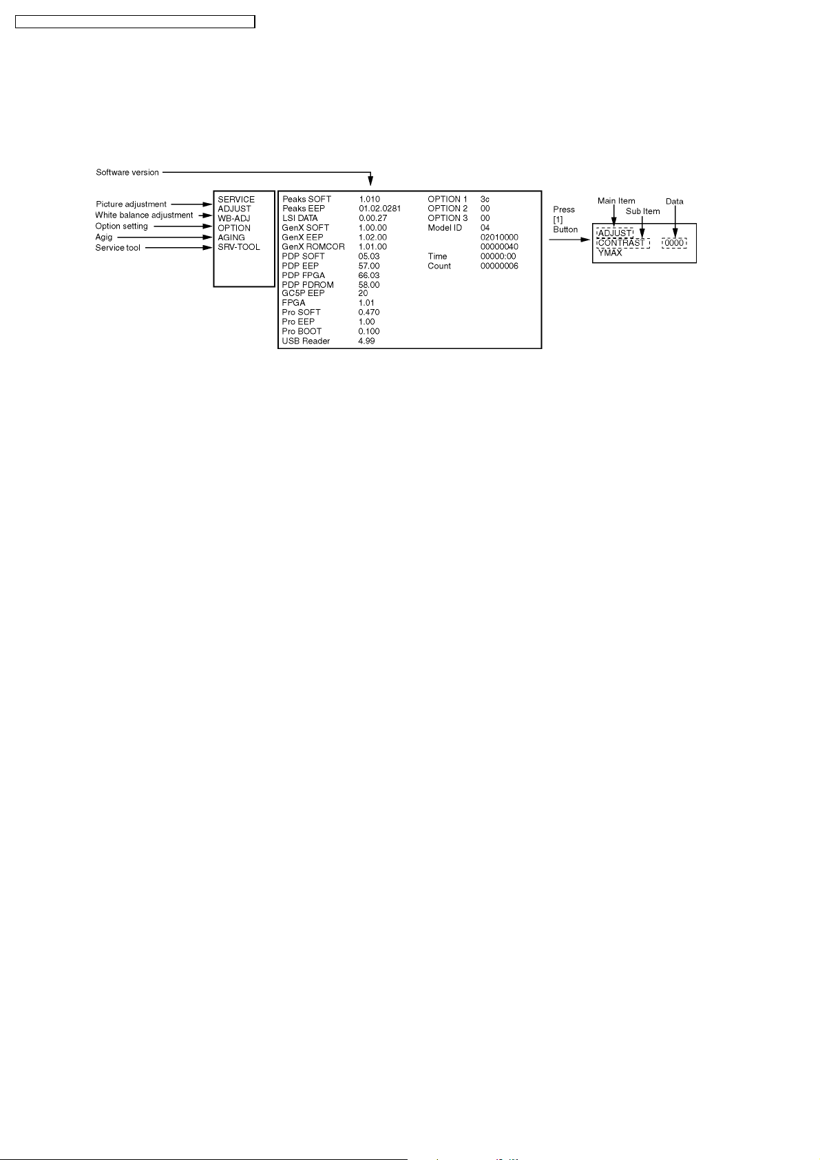
10 Service Mode
10.1. How to enter into Service Mode
While pressing [VOLUME ( - )] button of the main unit, press [0] button of the remote control three times within 3 seconds.
10.1.1. Key command
“1” button...Main items Selection in forward direction
“2” button...Main items Selection in reverse direction
“3” button...Sub items Selection in forward direction
“4” button...Sub items Selection in reverse direction
“RED” button...All Sub items Selection in reverse direction
“GREEN” button...All Sub items Selection in forward direction
“VOL” button...Value of sub items change in forward direction ( + ), in reverse direction ( - )
30
 Loading...