

Panasonic TH-50PV30E Schematic
Service Manual
TOP NEXT
\ORDER NO. 04-SM-008
Plasma TV
l
TH-50PV30E
GP6DE Chassis
Specifications
Power Source 220 V - 240 V 50 Hz/ 60 Hz A.C.
Power Consumption
Normal use 510 W
Standby 1.8 W (TV only)
Power-OFF 1.0 W
Plasma Display panel
Drive method AC type
Aspect Ratio 16:9
Contrast Ratio 3000:1
Screen size (No.of pixels) 50-inch
1,106 mm (W)× 622 mm (H)× 1,269 mm (diagonal)
1,049,088 (1,366 (W)× 768 (H)) [4,098× 768 dots]
Sound
Speaker Woofer
15.0 W (TV+ DVB system set to record Timer programmes)
80 mm× 2, Tweeter 16 mm× 73 mm× 8
Audio Output 26 W [ 8 W+8 W, 5 W+5 W ] (10%THD)
Headphone M3 (3.5 mm) Jack× 1
Applicable signals
Colour System NTSC, PAL, PAL60, Modified NTSC
Scanning format 525 (480)/60i
60p, 625 (575)/50i
50p
PC signals XGA display
VGA, SVGA, XGA
SXGA, UXGA ...... (compressed)
Horizontal scanning frequency 15 - 110 kHz
Vertical scanning frequency 48 - 120 Hz
Receiving Systems/Band name
PAL I UHF E21-68.
PAL 525/60 Playback of NTSC tape from some PAL Video recorders (VCR).
DVB Digital terrestrial services via UHF aerial input.
M.NTSC Playback from M.NTSC Videorecorders (VCR).
NTSC (AV INPUT ONLY) Playback from NTSC Videorecorders (VCR).
OUTPUT
AUDIO OUT AUDIO L-R (RCA Pin Type× 2) 0.5 Vrms
INPUT
AV3-Front VIDEO (RCA Pin Type× 2) 1.0 Vp-p (75Ω )
S-VIDEO (MINI DIN 4-pin) Y: 1.0 Vp-p (75Ω) C:0.286 Vp-p (75 Ω)
AUDIO L-R (RCA Pin Type× 2) 0.5 Vrms
AV4C-Rear Y 1.0 Vp-p (including synchronization)
PB/PR ±0.35 Vp-p
PC (HIGH-DENSITY D-SUB 15PIN) R, G, B/ 0.7 Vp-p (75 Ω)
HD, VD/ 1.0 - 5.0 Vp-p (high impedance)
Others SD Card slot× 1, PC Card slot× 1
INPUT/OUTPUT
AV1-Rear 21 Pin terminal (Audio/Video in, TV out, RGB in)
AV2-Rear 21 Pin terminal (Audio/Video in, Audio/Video out, S-Video in, Q-Link)
AV4-Rear 21 Pin terminal (Audio/Video in, Audio/Video out, S-Video in, RGB in, Q-Link)
ANT-Rear UHF
Operating Conditions Temperature :0° - 40°C
Humidity :20% - 80%RH (non-condensing)
Accessories Supplied
Operating Instructions TQBC0728
Mains Lead K2CT3DH00017
http://servis-manual.com/
8 Self Check
TOP PREVIOUS NEXT
1.Self-Check is used to automatically check the bus lines and hexadecimal code of the TV set.
2.To get into the Self -Check mode press the Down (
) button on the customer controls at the front of the set, at the same time pressing the
Status button on the remote control, andthe screen will show :
If the CCU ports have been checked and found to be incorrect or not located then “--” will appear in
place of “O.K.”.
Display Ref.No Description P.C.B.
MEM IC1008 EEPROM DG-BOARD
GC2M IC1301 GROBAL CORE MAIN DG-BOARD
GC2P IC1304 GROBAL CORE SUB DG-BOARD
GC2S IC1302 GROBAL CORE 3D Comb DG-BOARD
GC2V IC1350 GROBAL CORE V Scalar DG-BOARD
HAD IC1851 HD-AD CONVERTER DG-BOARD
LSYNC IC2652 SYNC PROCESSOR H-BOARD
AVSW IC3200 AV switch H-BOARD
YUVSW IC1270 YUV switch DG-BOARD
Tun1 TNR001 TUNER 1 TU-BOARD
VIF --- --- ---
DAC1 IC3003 Ext. DAC DG-BOARD
MSP IC2002 Multi Sound Processor H-BOARD
SOUND IC2401 AUDIO AMP PA-BOARD
PANEL --- PANEL ---
JPEG IC60 JPEG I/F JG-BOARD
8.1 Power LED Blinking timing chart
8.2 No Power
http://servis-manual.com/
8.2 No Power
TOP PREVIOUS NEXT
[First check point]
There are following 3 states of No Power indication by power LED.
1.No lit
2.Green is lit then turns red blinking a few seconds later.
3.Only red is lit.
1.No lit
TOP PREVIOUS NEXT
http://servis-manual.com/
8.3 No Picture
TOP PREVIOUS NEXT
TOP PREVIOUS NEXT
http://servis-manual.com/
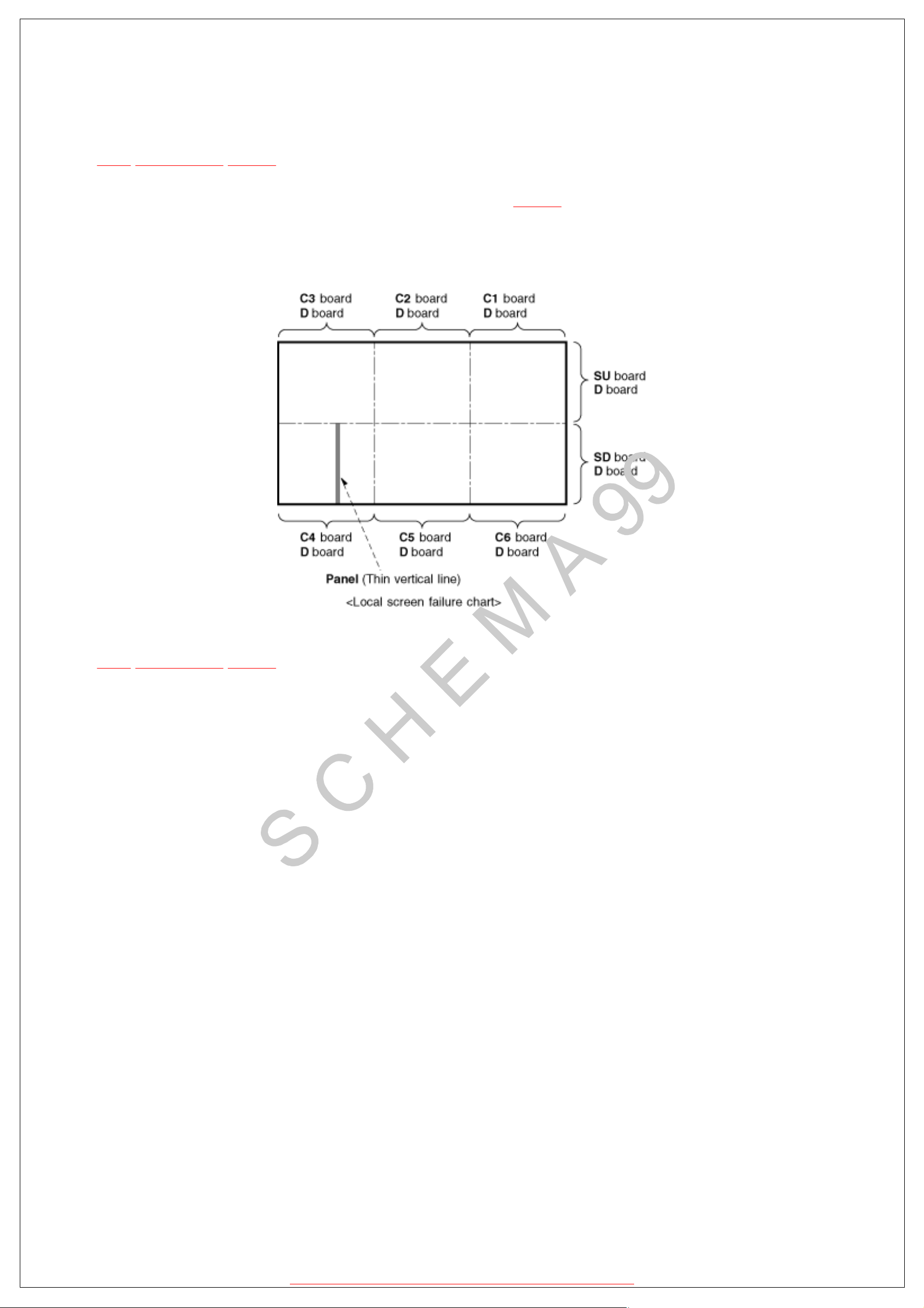
8.4 Local screen failure
TOP PREVIOUS NEXT
Plasma display may have local area failure on the screen. Fig - 1 is the possible defect P.C.B. for
each local area.
Fig - 1
TOP PREVIOUS NEXT
http://servis-manual.com/
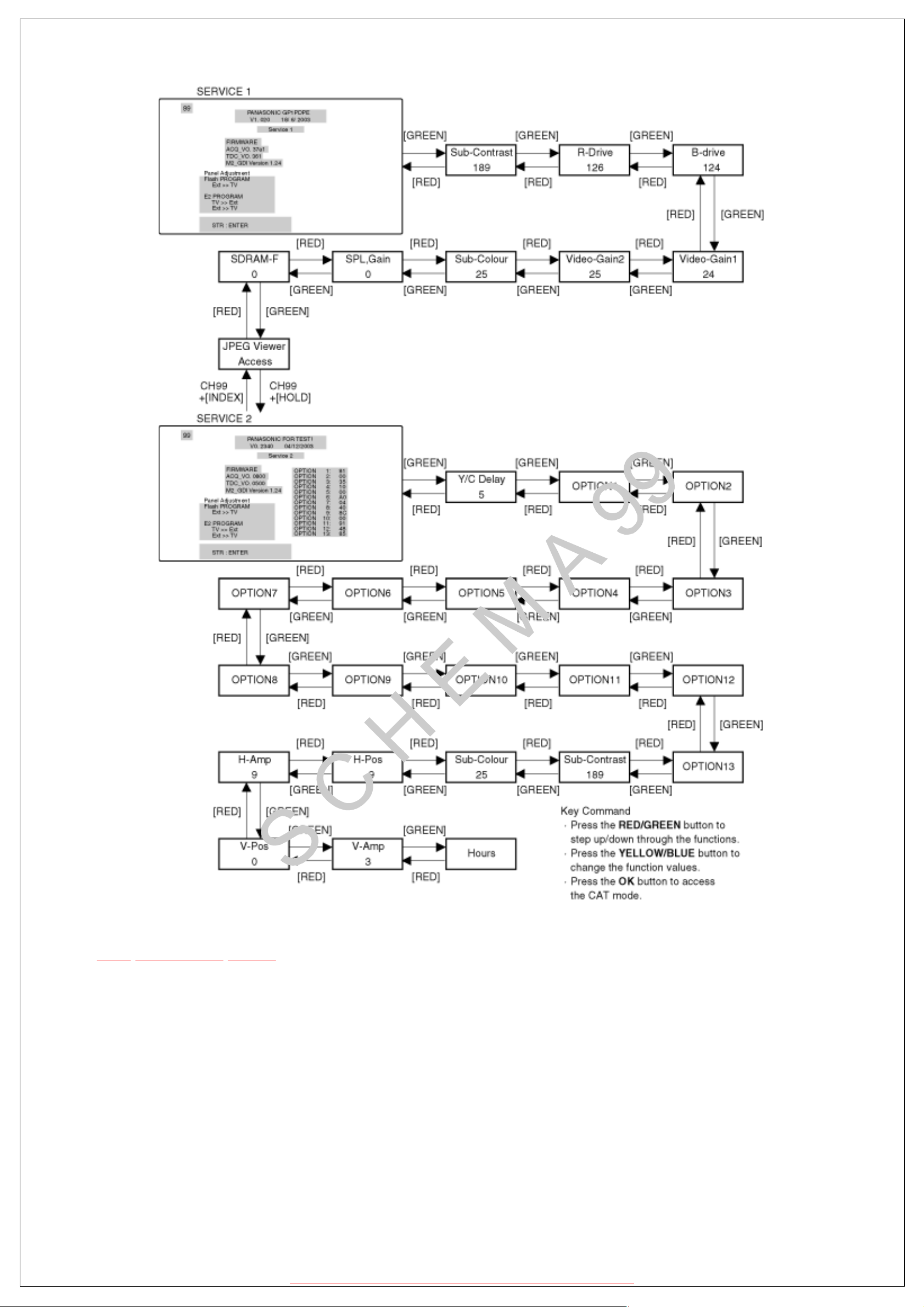
9.1 How to enter SERVICE 1
TOP PREVIOUS NEXT
1.In sound menu, set BASS to MAXIMUM, and set TREBLE to MINIMUM.
2.Simultaneously press INDEX button on remote control and DOWN button [
] on the TV set.
TOP PREVIOUS NEXT
http://servis-manual.com/

9.2 How to enter SERVICE 2
TOP PREVIOUS NEXT
1.Set the channel to CH99.
2.Select the JPEG Viewer.
3.Press HOLD button on remote control.
Note:
To exit to Service mode, press N or Power button on remote control.
http://servis-manual.com/
TOP PREVIOUS NEXT
http://servis-manual.com/
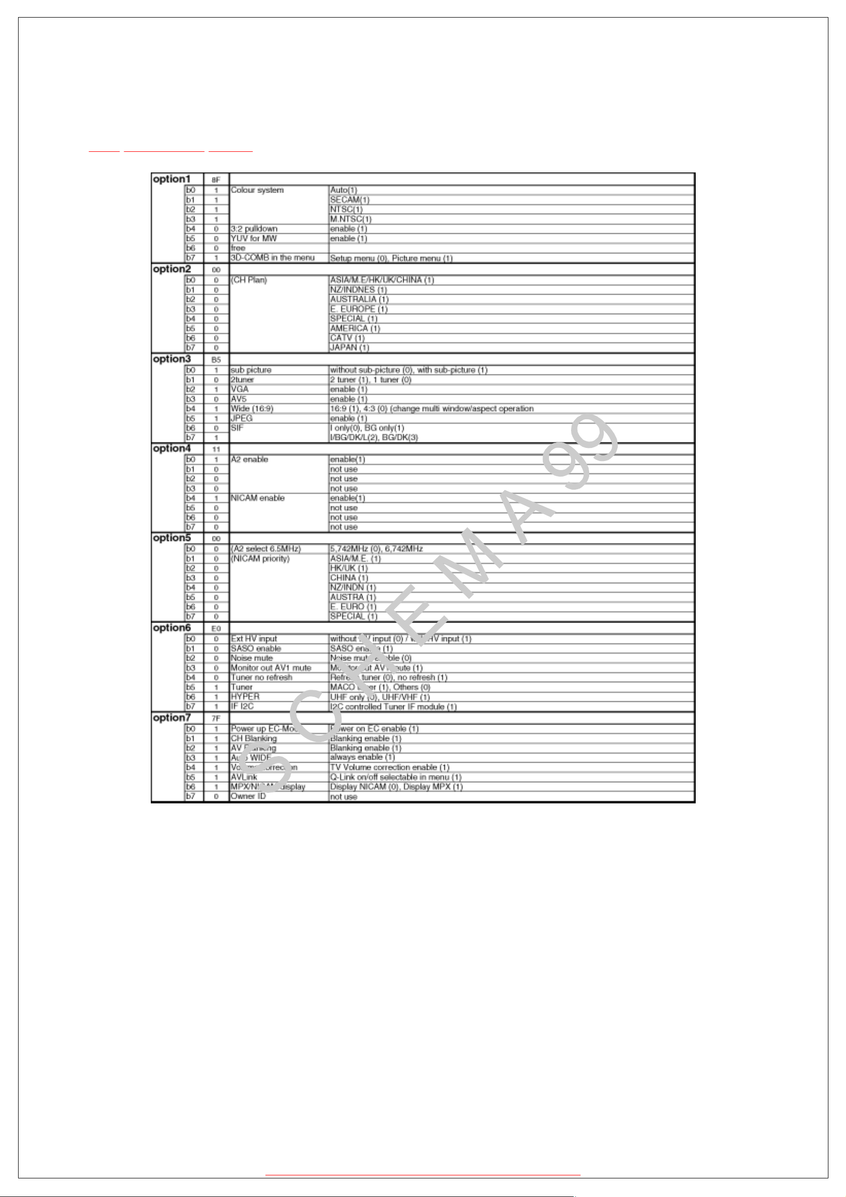
9.3 Option Description
TOP PREVIOUS NEXT
http://servis-manual.com/
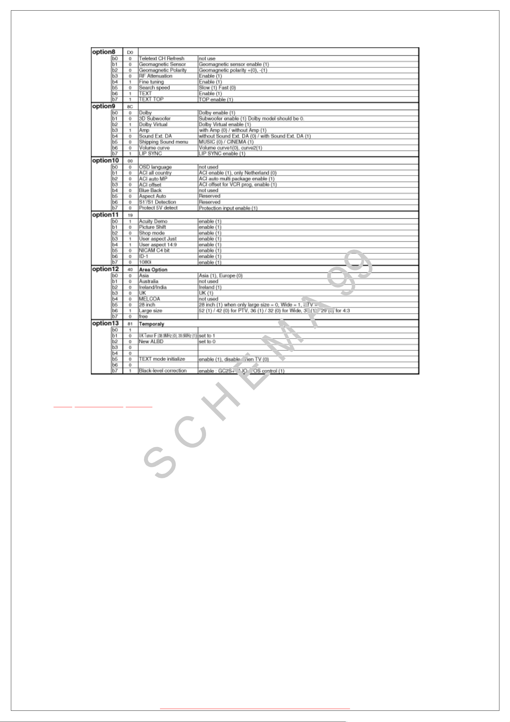
TOP PREVIOUS NEXT
http://servis-manual.com/
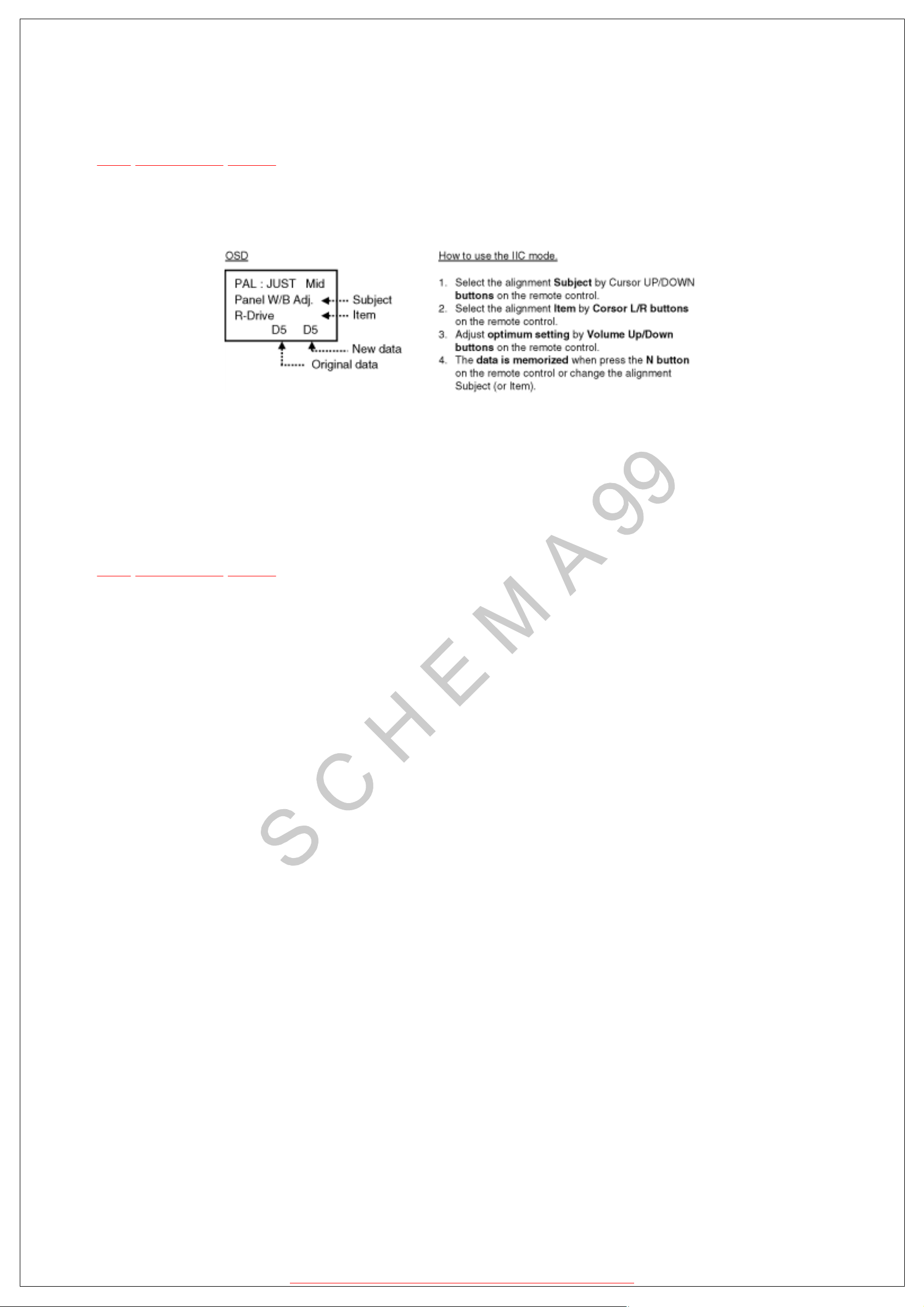
10.1 IIC mode
TOP PREVIOUS NEXT
Select the IIC mode by Up/Down (Channel) button on the remote control at the front page of CAT
mode then press the OK button on the remote control.
Subject and item are mentioned on IIC mode structure.
(Refer to item 10.4.)
To exit the IIC mode, press the MENU button on the remote control.
TOP PREVIOUS NEXT
http://servis-manual.com/

10.2 CD mode
TOP PREVIOUS NEXT
Select the CD mode by Up/Down (Channel) button on the remote control at the front page of CAT
mode then press the Mute
button on the remote control morethan 5 sec.
Micom software version (IC1007), this version can be upgrade by replace of new version IC
Memory data change
To exit the CD mode, press the MENU button on the remote control.
TOP PREVIOUS NEXT
http://servis-manual.com/
10.3 SD mode
TOP PREVIOUS NEXT
Select the SD mode by Up/Down (Channel) button on the remote control at the front page of CAT
mode then press the OK button on the remote control.
To exit the SD mode, press the MENU button on the remote control.
TOP PREVIOUS NEXT
http://servis-manual.com/
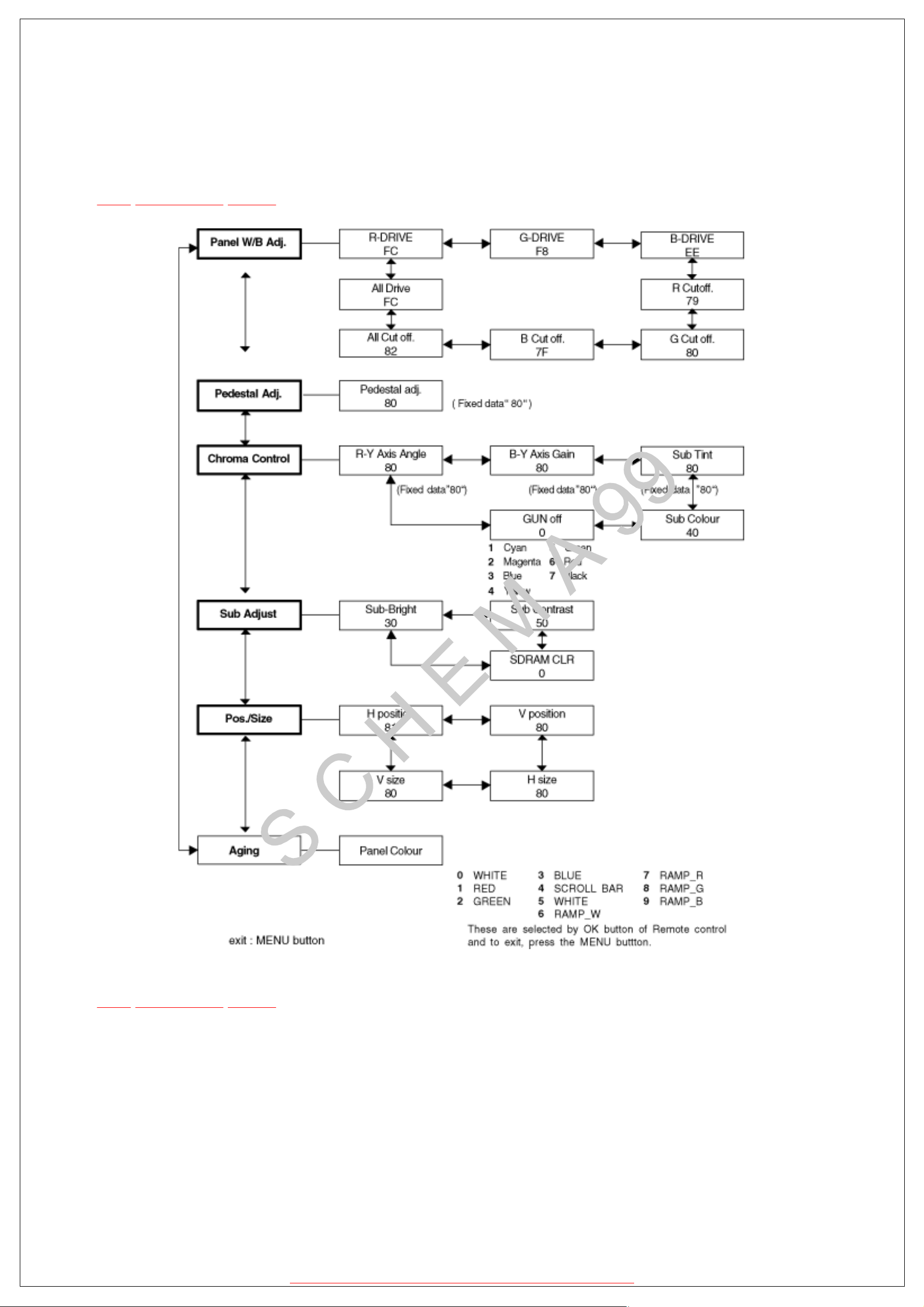
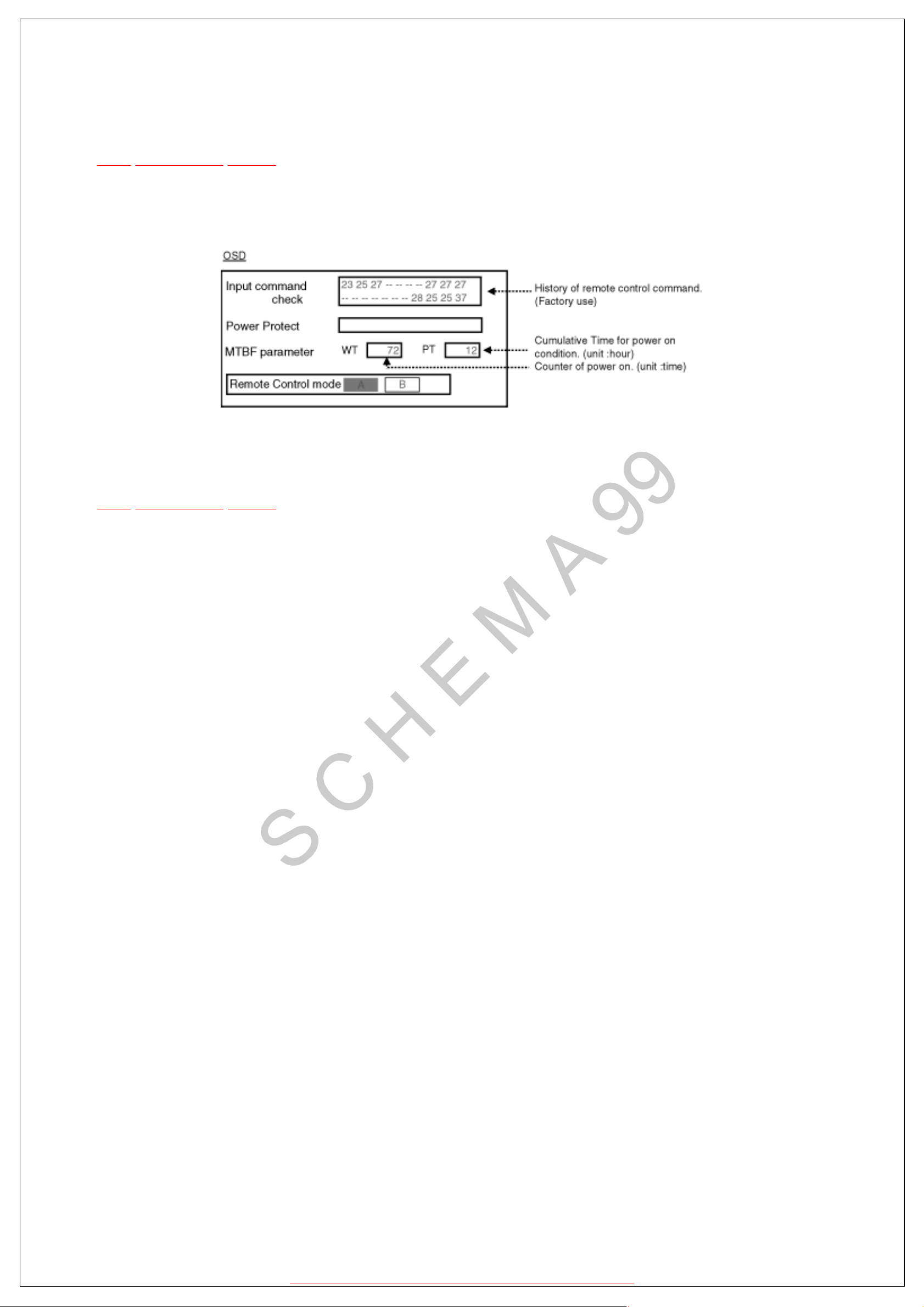
10.4 IIC mode structure (following items value
is sample data.)
TOP PREVIOUS NEXT
TOP PREVIOUS NEXT
http://servis-manual.com/
13 Hotel mode
TOP PREVIOUS NEXT
1.Purpose
Restrict a function for hotels.
2.Access command
¡ Enter to the Service 2 Mode.
¡
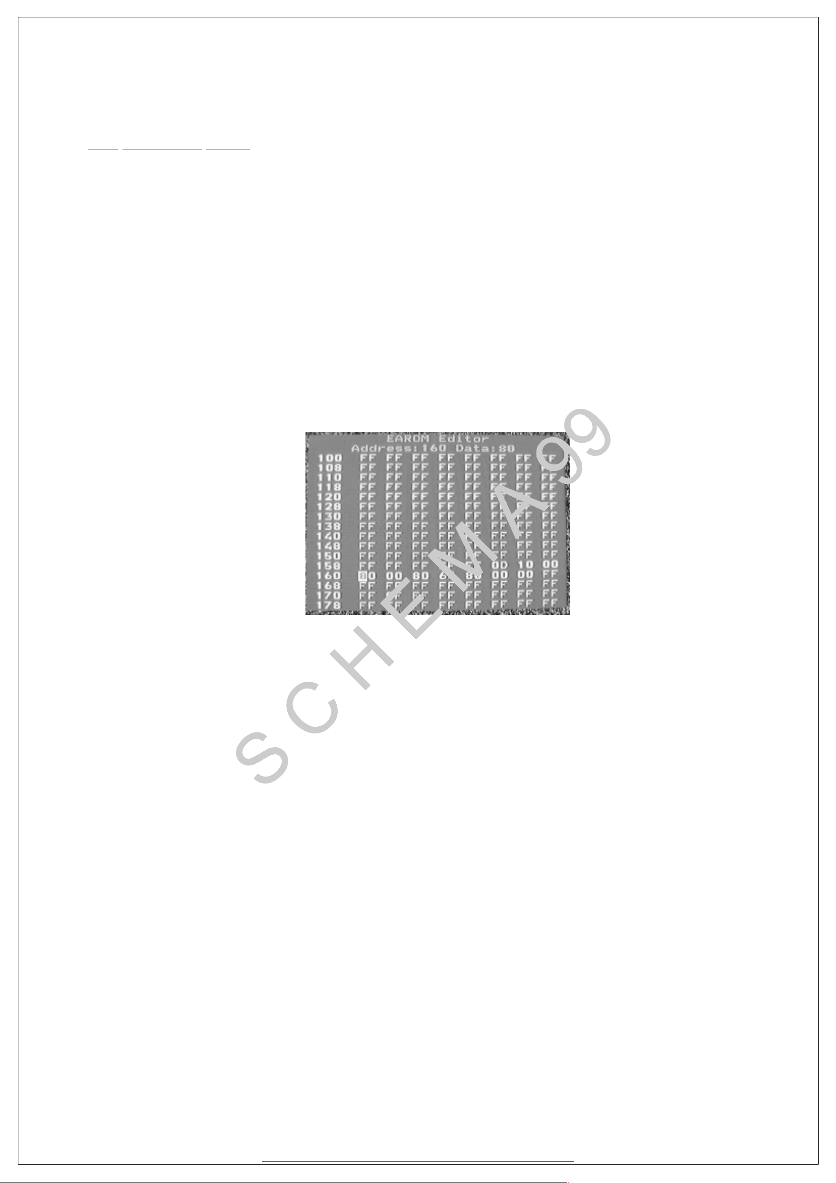
Press Status button on remote control and entry to the EAROM EDITOR Mode.
¡
Set the data of EEPROM(ADDRESS 160) to C0.
¡ Press the OK button to memorize the data.
Push the Power switch(button) off/on the set(the remote control) to turn the set off/on.
It can be made Hotel mode.
3.Exit command
¡ First, set the data of EEPROM(ADDRESS 160) to 80.
Next, Push the Power switch(button) off/on the set(the remote control) to turn the set
off/on.
Then, it is no longer hotel mode.
4.Access command to the Hotel mode setup menu
¡
<Prerequisite> : It is conditions that the data of EEPROM(ADDRESS 160) is C0.
In order to display the Hotel mode setup menu, please enter the following command
(within 2 second) .
[[TV]:down + [REMOTE]:TV/AV(3 times)]
Then, the Hotel mode setup menu is displayed.
http://servis-manual.com/

5.Explain the Hotel mode setup menu
CAUTION
This setup is not valid, unless data of EEPROM(ADDRESS 160) will be C0, even if each
settings were done.
item Function
Initial INPUT Select input signal modes.
Set this signal, each time power is switched on.
<Selection> :
Off/TV/AV1/AV2/AV2S/AV3/Av3S/AV4/Av4S/AV4C/PC
l Off: give priority to a last memory. However, Euro model is compulsorily set to TV.
l
AVnS/AVnC: only Euro model selectable
l PC: selectable with VGA option
Initial VOL
level
Maximum VOl
level
Initial POS Select programme number.
Adjust output Volume.
Set this volume, each time power is switched on.
If the value of InitVol is changed, volume will change. However, priority is given to a last memory when InitVol is Off. When"InitVol" is
larger than "MaxVol", make "InitVol" and "MaxVol" the same.
<Selection/Range> :
Off/0 to 100
l Off: give priority to a last memory
Adjust maximum volume.
Set this max. volume, each time power is switched on.
When "MaxVol" is smaller than "InitVol", make "MaxVol" and "InitVol" the same, if "InitVol" is not Off.
<Range> :
0to 100
Set this programme number, each time power is switched on.
<Selection> :
Off/0 to 99 (Euro model)
l Off: give priority to alast memory
Button lock Select local key conditions.
Set this condition, each time power is switched on.
<Selection> :
Off/SETUPMENU/All
l Off: altogether valid
l
SETUP: restrict F-key selection
(Tuning guide(menu) can not be selected.)
l MENU: restrict F-key selection
(only Volume/Mute can be selected.)
l All: altogether invalid.
http://servis-manual.com/
Remote lock Select remote control key conditions.
Set this condition, each time power is switched on.
<Selection> :
Off/SETUP/MENU
l Off: altogether valid
l SETUP: only Setup menu is invalid
l
MENU: Picture/Sound/Setup menu are invalid
TOP PREVIOUS NEXT
http://servis-manual.com/
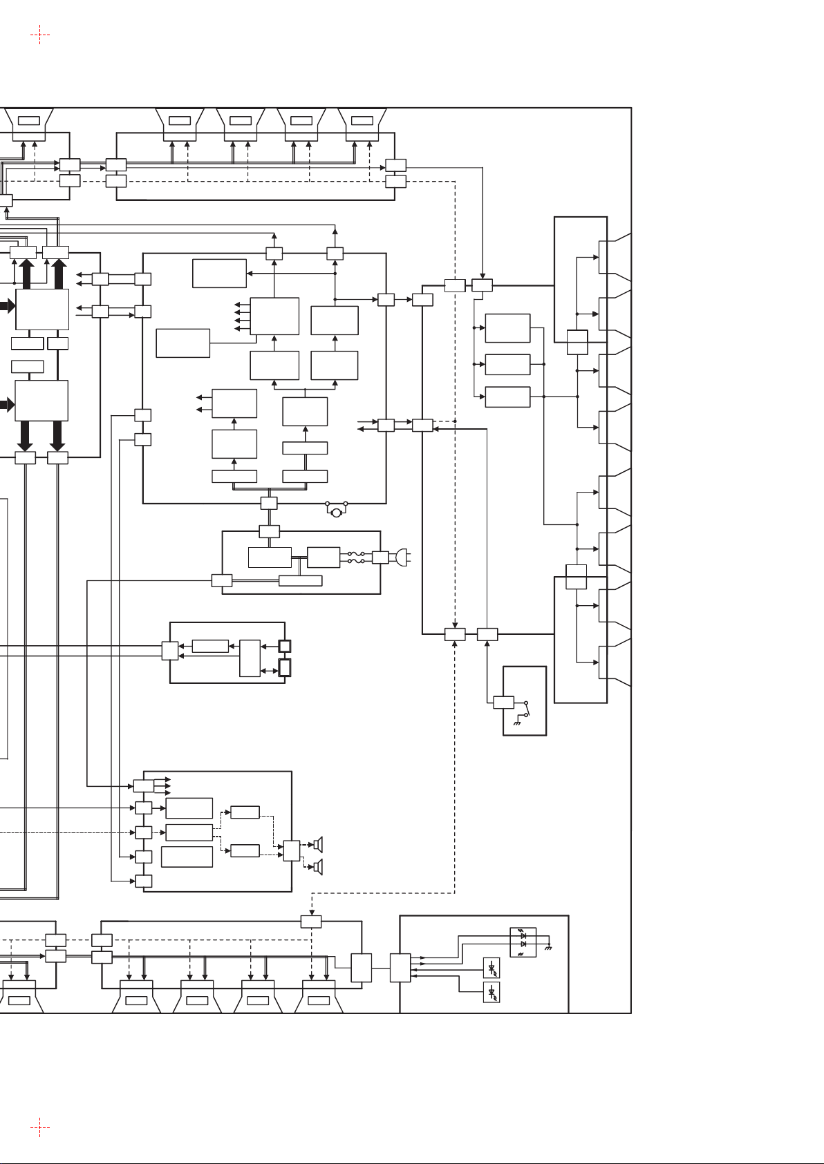
15 Block and Schematic Diagrams
15.1. Schematic Diagram Notes
75

75
15.2. Main Block Diagram
SU
S.R.
C12
C13
S.R.
S.R. S.R.
C10
C11
S.R.
C20
C22
C1
S.R
64
S.R
64
S.R
64
S.R
64
S.R
64
S.R
64
S.R
64
S.R
64
S.R
64
S.R
64
SC62
SC2
CONTROL
PULSE
INITIALIZE
PULSE
SCAN
VOLTAGE
SC23SC13SC12
SC20
D20
D
SYNC PROCESSOR/
DISCHARGE
CONTROL
VD
A/D
D3
HD
MAIN MPU
SUB MPU
HD/VD
CONTROL
ROM
24bit
BUS
SC
HEADPHONE
PC IN
G5
DG18
G18
C24
FORMAT
CONVERTER
RGB
PROCESSOR
SDRAM
S.R.
C25
S.R.
C2
D31
PLASMA AI
SUB-FIELD
PROCESSOR
SDRAM
SDRAM
PLASMA AI
SUB-FIELD
PROCESSOR
D34
C21
C23
D32
ROM
D33
SD
S.R
64
S.R
64
T
MAIN
TUNER
AUDIO
OUT
T10
H10
MSP
AV1
AV2
AV4
KEYSCAN
VIDEO3
G
H9
AV
SWITCH
DG7
G7
DG1
H1
DG4
H4
CONVERT
EEPROM
SDRAM
GC2M
GC2S
SDRAM
MICOM
RGB AMP
DG
MICOM
TEXT
RGB/PC
SELECT
TV ON
DG10
DG3
DG2
DG6
H
C6
C62
S.R.
S.R.
S.R. S.R. S.R.
C61
C60
C5
C52
C50
C54 C55
S.R.
C53
C51
S.R.S.R.
TH-50PV30E
Main Block Diagram
76
S.R.
S.R.
S.R.
S.R.
S.R.
C2
D31
PLASMA AI
SUB-FIELD
PROCESSOR
SDRAM
SDRAM
PLASMA AI
SUB-FIELD
PROCESSOR
D34
D32
ROM
C21
C23
C31
C33
C32
C35
C3
SS2
P23 P2
PROCESS
VOLTAGE
RECTIFIER
PROCESS
VOLTAGE
CONTROL
P9
PF2
PRIMARY
CIRCUIT
AC IN
15V
POWER
FACTOR
CONTROL
RECTIFIER
RELAY
STAND BY
LOW
VOLTAGE
PROTECTOR
P
HIGH
VOLTAGE
PROTECTOR
VDA
15V
12V
5V
STANDBY
VOLTAGE
RECTIFIER
STANDBY
VOLTAGE
CONTROL
RECTIFIER
UR12V
5V
P25D25
STB7V
ON/OFF
P27D27
SOS
STB5V
+12Vs
12V
P7
STB5V
P5
15V
D33
PF
PF10
SUSTAIN
VOLTAGE
RECTIFIER
SUSTAIN
VOLTAGE
CONTROL
P30-P33
LINE
FILTER
FAN
VSUS
SS32
VSUS
P11
VDA
P12
STB PS
M
AC IN
PF1
SS11
SS12
SS35
SS
ADDRESS
VOLTAGE
(VE)
SUSTAIN
PULSE
ERASE
PULSE
SS21
SS57
SS58
SS31
JG
PA
PA1
PA3
SD CARD
PC CARD
C42
SPEAKER
SPEAKER
VDA
K24
C44
Y/C OUT
JG3
NR 21V
STB 5V
PA10
NR 14V
PA2
TUNER 30V
PRE AMP
PA6
DC/DC
PA5
CONVERTER
PA7
C53
C51
S.R.S.R.
C4 K
C43
C41
S.R.
I/F
L OUT
R OUT
S.R. S.R.
SS42 SS34
POWER ON
STAND BY
S34
REMCOM
RECEIVER
CAT
SENSOR
S
POWER
SWITCH
LED
SS3
G
R
76
TH-50PV30E
Main Block Diagram
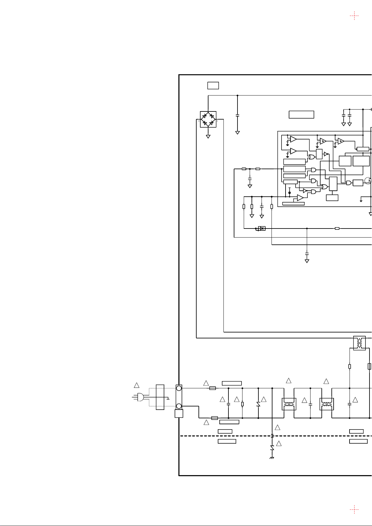
15.3. PF-Board Block Diagram
PF Tuner Power Supply
D920
-+
+
C920
R928
R927
C926
R934
R935
C924
D926
IC920
POWER CONTROL
Latch-stop
+
comp
VUL
OVP
comp
+
-
VOVP
Thermal
Shutdown
Z/C
1
Zero Current
Detection
On Dead Timer
Stand-By
Vref
IF/B
2
F/B
+
On Time Timer
R929
C925
DC187V
D925
+
C928
UVLO
comp
+
-
Vcc(start)
/Vcc(stop)
R
Q
S
S
R
S
Restart
Timer
R925
+
-
Vcc(startup off)
/Vcc(startup on)
Peak
Current
Limit
Q
Startup
UVLO
comp
C922
Vcc
Startup
Burst Peak
Current
Limit
Soft
drive
5
4
D
GND
3
TH-50PV30E
PF-Board Block Diagram
!
AC CORD
AC INLET
1
4
L.F
3
2
LF911
R904
T8AH 250V
!
AC120V
4
NEUTRAL
GND
1
LIVE
PF1
F901
! ! !
C901
T8AH 250V
F900
!
R901
CF901
$
HOT
COLD
!
LF904
3
L.FL.F
2
!
S901
!
CF902
4
!
C902
1
!
LF909
4
3
2
1
!
C915
HOT
COLD
77
+
+
-
Vcc(startup off)
/Vcc(startup on)
Peak
Current
Limit
Startup
UVLO
comp
C922
Vcc
Startup
Burst Peak
Current
Limit
Soft
drive
HOT COLD
T920
!
18
P2
17
S3
D925
400V
5
4
D
GND
3
D922
C921
L921
R924
#
R940
IC921
!
NC
16
S4
PT
15
NC
14
S1A
P1
13
NC
S1B
12
S2A
NC
11
S2B
V2
10
V1
!
C914
HOT COLD
1
4
FEED BACK
2
3
C972
2
3
5
6
7
8
R971
+
D971
C973
C970
D970
+
C971
14V(UN REG)
21V(UN REG)
R970
R972
C975
PF10
5
1
2
TO PA10
UNR_14V
UNR_21V
UNR_21V
R976
C974
R973
STAND-BY 5V
+
C990
R990
R992
3
1
REF_2.5V
2
IC970
ERROR
VOLTAGE
!
RL901
1
4
L.F
3
2
LF911
!
R904
F902
K5D312BK0012
HOT COLD
DET
D990
Q990
POWER ON/OFF CONTROL
T3.15AL 250V
!
LF915
!
C915
3
L.F
2
NEUTRAL
4
!
C903
1
LIVE
HOT
COLD
!
C911
!
C910
HOT
COLD
COLD
HOT
R974
R975
7
STB_5V
9
AC_ON/OFF
TO P9
PF2
1
NEUTRAL
LIVE
4
77
TH-50PV30E
PF-Board Block Diagram
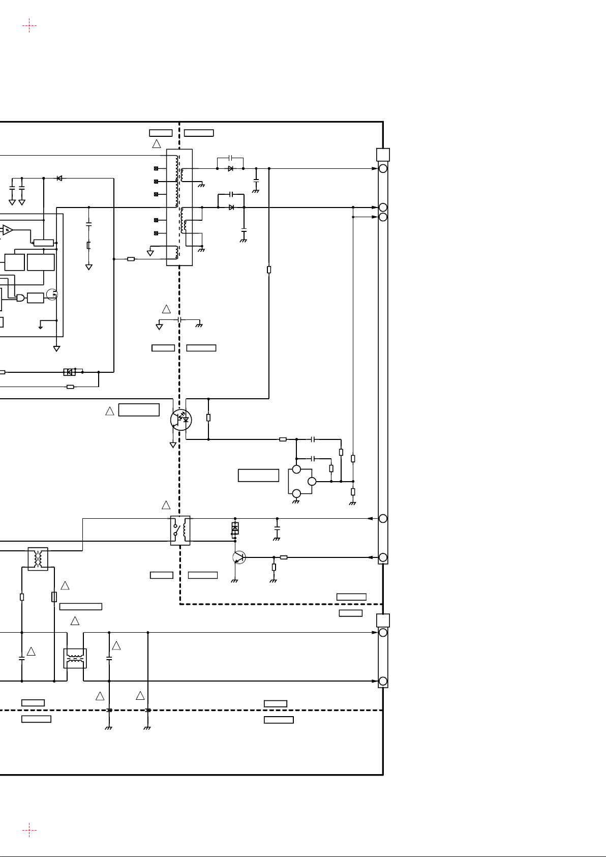
15.4. PF-Board Schematic Diagram
PF-BOARD TNPA2926AB
A
B
C990
50V
10u
D990
MA3X152K0L
Q990
2SD13280TL
R990
3.3k
R992
47k
C
COLD
RL901
K6B1ADA00023
**
B0EBNT000002
TP904
D920
*
*
*
-
*
C920
****
450V
150u
R938
100k
C930
50V
0.01u
RTFC
7
R920
100k
R921
100k
**
IC920
C5HABZZ00121
4
Vcc
+
-
OVP
TSD
+
-
OLP
Current
Mirror
FB/OLP
R936
22k
+
C929
50V
10u
TP901
+
C921
C922
50V
50V
33u
0.1u
POWER CONTROL
LATCH
DRIVE REG
R
Q
S
REG
REG
Current
Mirror
OSC
RESET
BEC
73uA
6
R935
1k
=
C931
50V
150p
+
TFC
-
BTC
BD
C928
D929
50V
B0BA01000046
2200p
D
1
OCP/BD
-0.65V
S/GND
*
3
*
C926
50V
470p
5
R934
150
D926
B0HCMM000001
=
#
R933
180
R940
100
DRV
OCP
+
-
1
4
1
4
*
*
LF911
G0B353G00001
D
E
R993
0
R994
0
JS70
JS73
K4ZZ01000121
R904
TO
P-BOARD
(P9)
NEUTRAL
PF2
1
C910
**
250V
220p
C911
250V
220p
ZA901
C903
250V
**
3
1u
4
**
LIVE
3.3
*
10 3
1*2
8
L.F
2
3
*
*
3
2
T3.15AL-250V
F902
** **
<
3*4
LF915
G0B123K00001
L.FL.F
9
*
K5D312BK0012
C917
470p
F/S_HOT:920-969
C915
250V
**
0.22u
C916
470p
HOT
LIVE CIRCUIT
LF:900-919
*
3
4
<
3**4
LF909
G0B123K00001
1*2
1
*
2
TH-50PV30E
PF-Board Schematic Diagram
1 65
78

C923
R922
400V
220k
0.01u
*
*
R923
10
D921
B0EAKT000018
L920
J0JKB0000038
585Vp
TP901
+
C921
C922
50V
50V
33u
0.1u
C924
2kV
D
1
*
3
*
C926
5
R934
150
D926
B0HCMM000001
**
470p
L921
EXCELSA24T
50V
470p
=
R932
0.82
*
#
R933
180
R940
100
**
D922
B0HCMM000001
R924
3.3
-140Vp
D925
B0HCMM000001
=
=
R939
R931
0.82
0.68
*
*
R927
560
R928
470
C927
220p
50V
L922
EXCELDR35V
ETS29AK7E6AD
*
*
T920
18 P2
17 NC
16 PT
15
14 P1
13 NC
12 NC
11 V2
10 V1
C914
250V
220p
2S3
3S4
NC
5S1A
6S1B
7S2A
8S2B
L972
L970
EXCELSA24T
C972
1kV
330p
D971
B0HAPM000012
0
-140Vp
GT GT
C970
1kV
D970
FMLG12SLF118
+
330p
**
+
14V_0.9A
C973
25V
1000u
20.5V_1.4A
C971
35V
JS80
1200u
TP979
R970
680
TP977
L973
10u
TP978
L971
10u
TO
PA-BOARD
PF10
(PA10)
20.5
1
NR_20.5V
20.5
2
NR_20.5V
0
3
GND
0
4
GND
14.0
5
NR_14V
0
6
GND
5.0
7
STAND-BY 5V
0
8
GND
2.0
9
PF_AC_ON/OFF
FEED BACK
1
IC921
B3PAA0000261
HOT
LIVE CIRCUIT
4
3
2
COLD
R971
470
R972
100
3
IC970
AN1431M-E1
ERROR
VOLTAGE
DET
CATHODE
ANODE
2
1
REFERENCE
C974
3300p
REF_2.5V
50V
R974
R973
2.2k
16.9k
R975
2.32k
78
C902
250V
**
0.22u
C901
250V
**
1u
T8AH 250V
F901
K5Y802B00001
F900
K5Y802B00001
T8AH 250V
LIVE
JS9
JS10
JS11
JS12
3
4
*
3*4
LF904
L.F
G0B123K00001
1*2
1
2
*
S901
J0LT00000009
S915
J0LT00000009
CF902
ERZV10V621P2
LF:7000-7019
CF901
ERZV10V621P2
R902
1M
**
R901
1M
**
COLD
AC100V-240V
HOTCOM100V-240V
1**3
PF1
LIVE CIRCUIT
HOT
NEUTRAL
4
**
TH-50PV30E
PF-Board Schematic Diagram
742
83
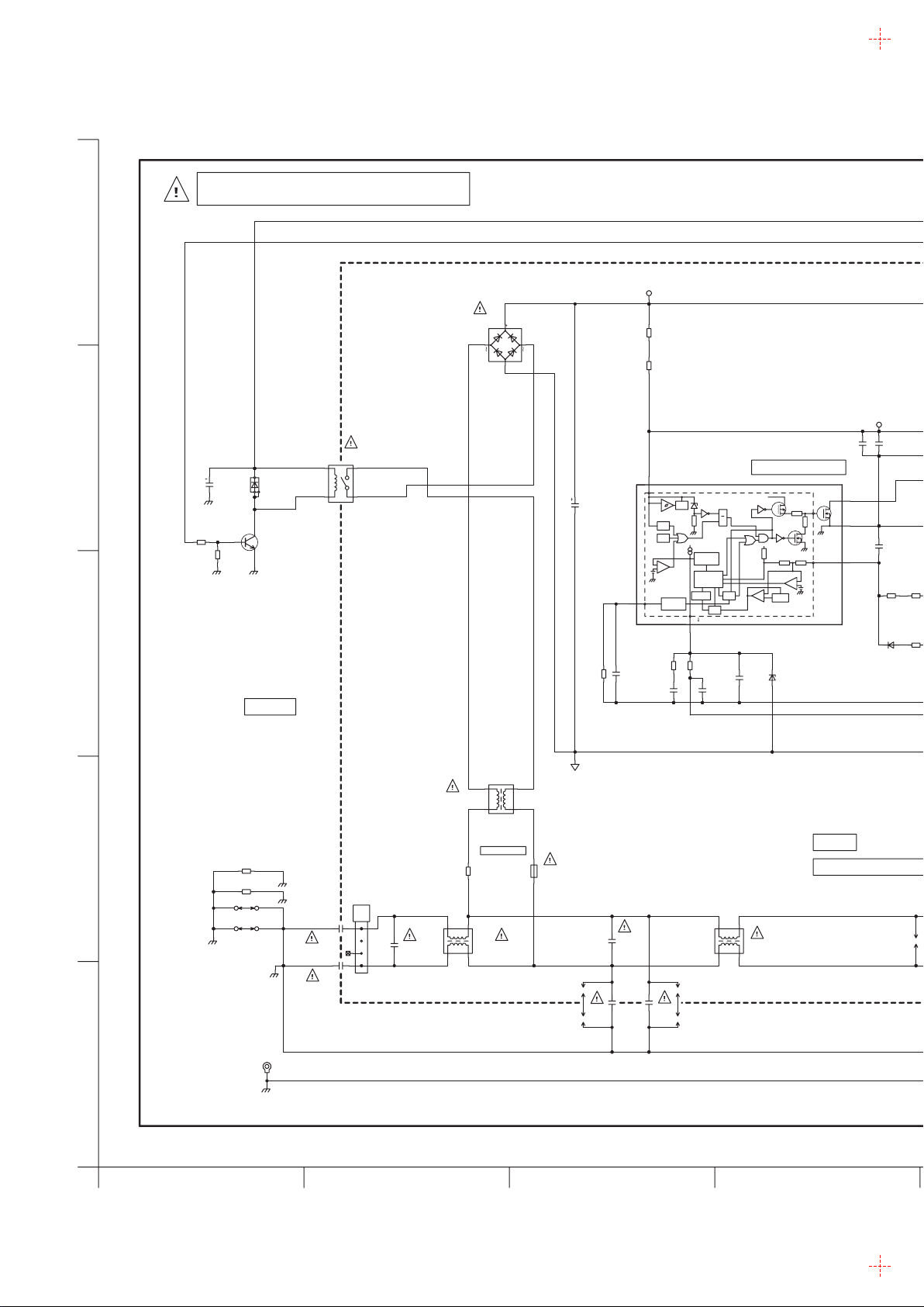
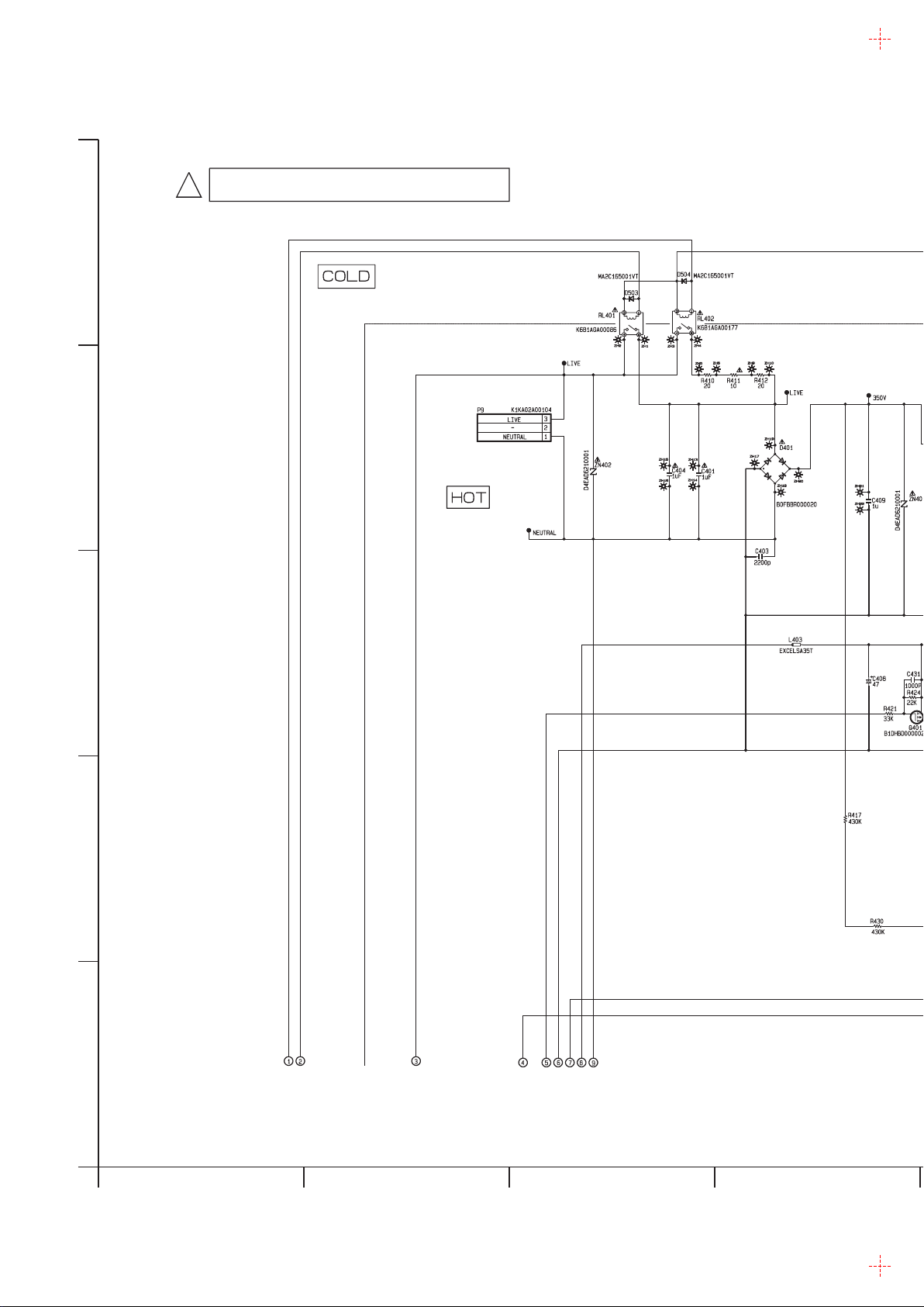
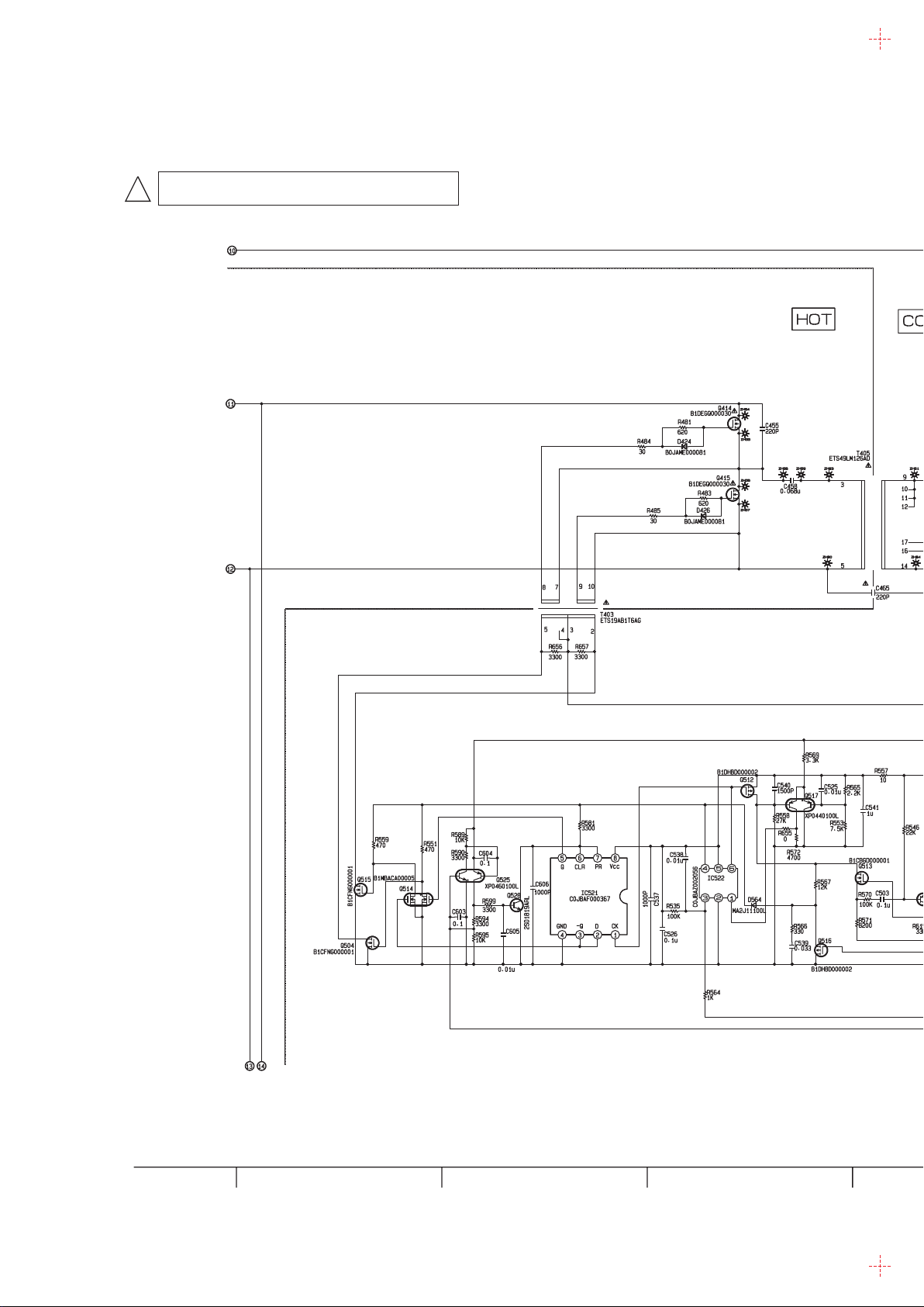
15.5. P-Board Block Diagram
350V
T401,T406
Q401
AMP
Q420
R443
PFC
D419
D420
L403
DC400V
PR401
Q410
Q411
DRIVE
!
Q414
!
Q415
!
!
T402
DC180V
!
T405
D539
2
16
D537
6
12
!
T403
Q515
2
10
9
3
7
8
5
Q504
PFC
16
VCC
MOS
DRIVE
2134
3981442
CURR
CURR
COMP
DET
5876
Q404
Q406
L402
D415
IC406
POWER
FACTOR
CONTROL
!
F405
10
Q407
Q421
TO
PF2
IC402
8
1
72
3
6
4
5
14
15
13
10
1
23
!
RL401
D511
D510
IC408
!
D434
IC504
D557
R
KA
!
RL402
STB7V
!
LIVE
NEURTAL
31
P9
D401
- +
NEUTRAL
LIVE
P
Power
Supply
!
D404
- +
Q416
!
D410
350V
IC409
4
Q403
D409
!
T410
8
6
5
2
1
4
3
4
Board
134
2
134
2
421
3
IC404
!
IC403
!
STB7V
IC401
!
IC502
RESET
D555
Q535
Q501 Q522
Q503Q502
STB5V
IC501
POWER MPC
VDD
P00
1
VSS
P01
1
3
2
XIN
P02
3
X501
4NHz
XOUT
P03
4
P10
5
RESET
P11
6
P21
P12
7
P20
P13
8
D3
D0
9
D2
D1
10
COLDHOT
TH-
50PV30E
P-Board Block Diagram
79
COLDHOT
R641
Vsus
Q542
!
Q541
DC75V
R665
DC15V
Q509
Q508
Q524
Vda
R661
Vlow
Q520
1
3
!
PR510
R608
Csus
2
D549
D554
D565
DC85V
D534
DC12V
IC511
14
5VAVR
D541
D533
DC15V
13
64
CK
IC523
CLRPR
7316
2
D
D536
Q527
DC5V
Q543
IC520
Q540
Q
Q
5
K
A
D543
D544
D545
R
IC512
D535
PR509
5
2
!
T407
Q510
D531
7
9
8
13
12
11
14
D563
!
T404
!
Q412
!
Q413
9
710
3
185
!
T402
DC180V
D539
2
D537
6
Q515
2
3
5
Q504
Q514
D521
D530
Q519
Q545
251
46
Q518
Q525
Q528
7
6
5
PR
Q
CLR
CK
Q
D
31
2
Q521
Q512
64
IC522
13
D564
Q516
Q513 Q506
Q511
P12
P23
P11
P25
TO
SS12
1
Vda
2
Vda
STB_PS
10
+15V
4
P7
1
+15V
2
+15V
TO
SC23
1
+15V
2
+15V
TO
SS11
1
Vsus
2
Vsus
TO
P2
SC2
1
Vsus
2
Vsus
TO
Z5
P5
1
+12V
2
+12V
3
5V
+12Vs
7
8
+12Vs
11
+15V
TO
D25
1
+12V
2
+12V
5
5V
FAN CONT
7
8
STB7V
Q517
Q551
D505
D506
IC501
POWER MPC
VDD
P00
1
1
3
2
3
X501
4NHz
4
5
6
7
8
9
10
VSS
XIN
XOUT
RESET
P21
P20
D3
D2
20
P01
19
TV ON/OFF
P02
18
V SUS
P03
17
STB5V
P10
16
PS SOS
P11
15
P12
14
P13
13
D0
12
ALL OFF
D1
11
STB7V
Q544
P30
FAN SOS
3
VCC
1
P31
FAN SOS
3
VCC
FAN SOS
FAN SOS
1
P32
VCC
P33
VCC
!
3
PR502
1
D553
3
1
FAN
Q530
Q531
ALL OFF
Q532
TH-
50PV30E
TO
D27
P27
2
TV ON/OFF
4
Q537Q552
Q546
STB5V
6
FAN SOS
PS SOS
7
8
ALL OFF
M.POWER
3
P-Board Block Diagram
79
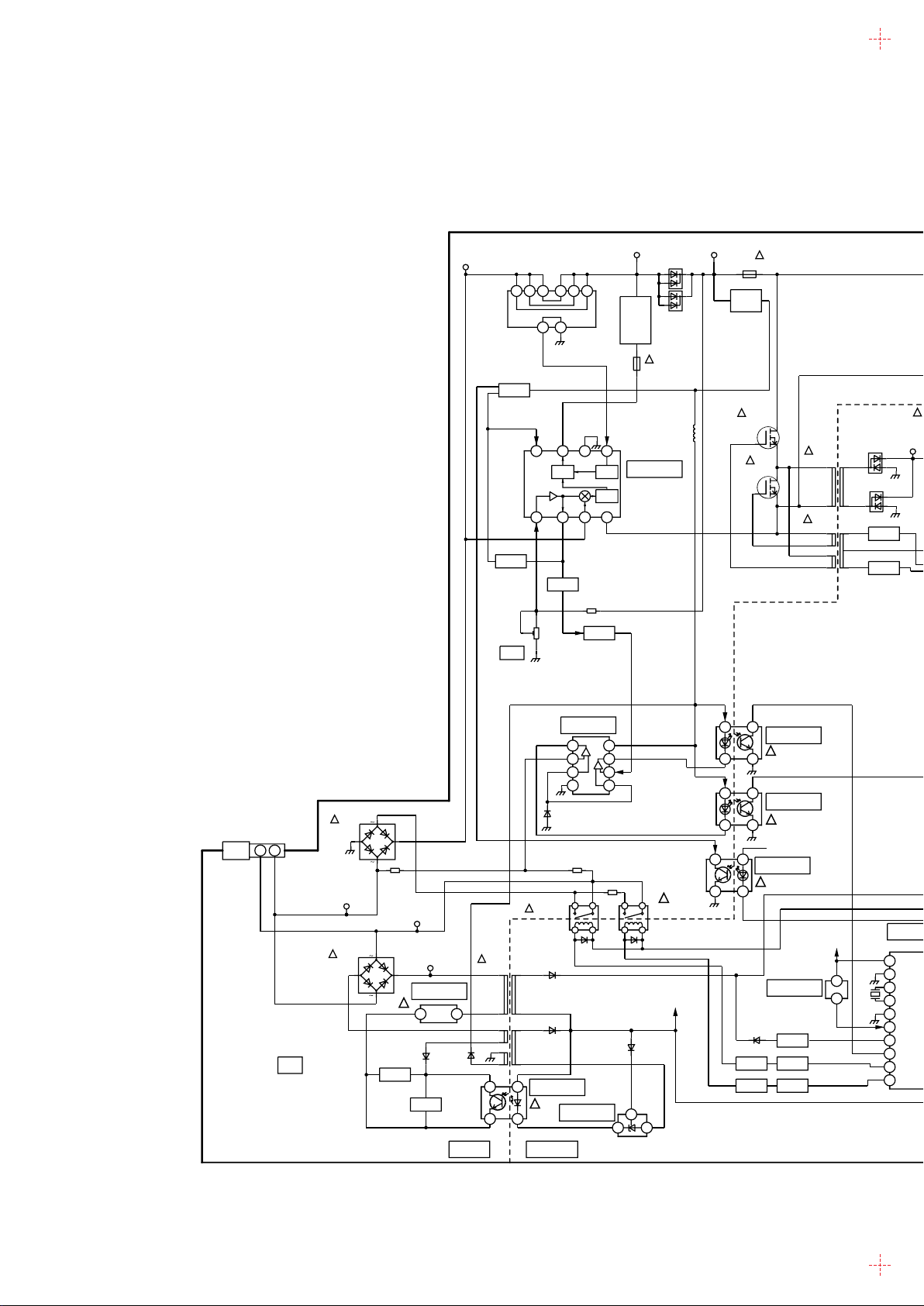
15.6. P-Board (1 of 6) Schematic Diagram
P-BOARD TNPA2890 (1/6)
!
A
B
TO
PF-BOARD
(PF9)
C
D
E
TH-50PV30E
P-Board (1 of 6) Schematic Diagram
1
2 8
3 7
4
80

80
TH-50PV30E
P-Board (1 of 6) Schematic Diagram
56
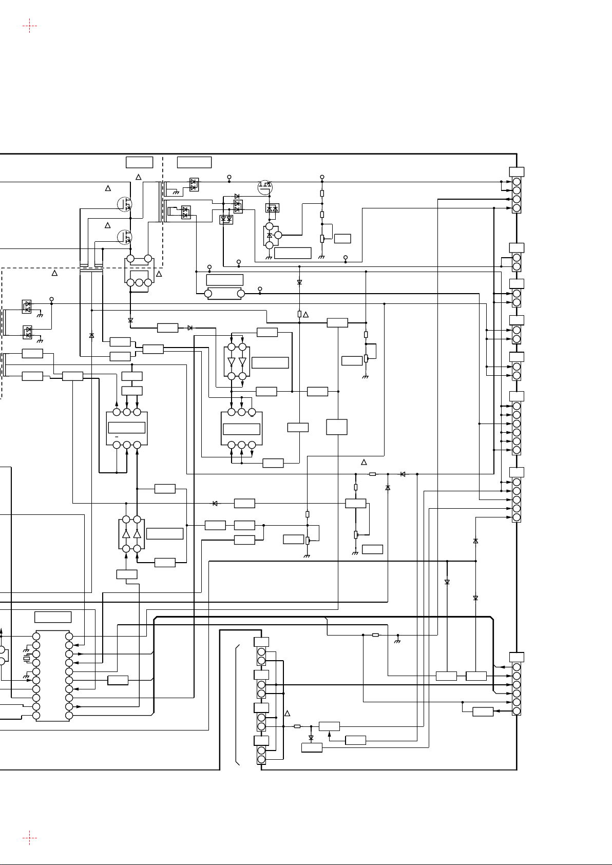
15.7. P-Board (2 of 6) Schematic Diagram
P-BOARD TNPA2890 (2/6)
!
TH-50PV30E
P-Board (2 of 6) Schematic Diagram
8
4.8
4.3
4.8
4.8
4.8
4.8
2.4
4.3
4.9
14.3
0
0
14.3
0
00
2.3
2.3
2.2 2.2
0
4.7
0
0
4.8
2.4
2.4
0
4.1
000
4.44.4
0
3.8
0
0
4.3
2.0
0.8
4.1
4.7
0
0
5.5 5.5
2.0
10 11 12 13
81
 Loading...