

Page 1

ORDER NO.MTNC090327CE
B05 Canada: B07
32 inch Class 720p LCD HDTV
Model No. TC-L32C12
LH90 Chassis
© Panasonic Corporation 2009.
Unauthorized copying and distribution is a violation
of law.
Page 2

TABLE OF CONTENTS
PAGE PAGE
1 Safety Precautions -----------------------------------------------3
1.1. General Guidelines ----------------------------------------3
2 Warning --------------------------------------------------------------4
2.1. Prevention of Electrostatic Discharge (ESD)
to Electrostatically Sensitive (ES) Devices ----------4
2.2. About lead free solder (PbF) ----------------------------5
3 Service Navigation------------------------------------------------6
3.1. Service Hint--------------------------------------------------6
3.2. Applicable signals------------------------------------------6
4 Specifications------------------------------------------------------7
5 Service Mode-------------------------------------------------------8
5.1. How to enter into Service Mode------------------------8
5.2. SRV-TOOL---------------------------------------------------9
5.3. Hotel mode-------------------------------------------------10
6 Troubleshooting Guide---------------------------------------- 11
6.1. Check of the IIC bus lines------------------------------ 11
6.2. Power LED Blinking timing chart-------------- -------12
6.3. No Power--------------------------------------------------- 13
7 Disassembly and Assembly Instructions---------------14
7.1. Pedestal ----------------------------------------------------14
7.2. Rear cover ------------------------------------------------- 1 4
7.3. AC cord-----------------------------------------------------14
7.4. P-Board-----------------------------------------------------15
7.5. Side AV bracket-------------------------------------------15
7.6. A-Board-----------------------------------------------------15
7.7. Control panel---------------------------------------------- 16
7.8. Speaker-----------------------------------------------------16
7.9. A-P-MTG Metal -------------------------------------------16
7.10. VESA metal ------------------------------------------------ 16
7.11. LCD MTG -------------------------------------------------- 17
7.12. LCD Panel -------------------------------------------------17
7.13. V-Board-----------------------------------------------------17
7.14. EMI processing -------------------------------------------18
8 Measurements and Adjustments --------------------------21
8.1. Voltage chart of A-board--------------------------------21
8.2. Picture level adjustment (RF) -------------------------21
8.3. Picture level adjustment (VIDEO)-------------------- 22
8.4. Picture level adjustment (YUV) -----------------------22
9 Block Diagram ---------------------------------------------------23
9.1. Main Block Diagram-------------------------------------23
9.2. Block (1/2) Diagram -------------------------------------24
9.3. Block (2/2) Diagram -------------------------------------25
10 Wiring Connection Diagram---------------------------------27
10.1. Caution statement.---------------------------------------27
10.2. Wiring -------------------------------------------------------27
11 Sch ematic Diagram--------------------------------------------- 29
11.1. Schematic Diagram Notes----------------------------- 29
11.2. A-Board (1/10) Schematic Diagram -----------------30
11.3. A-Board (2/10) Schematic Diagram -----------------31
11.4. A-Board (3/10) Schematic Diagram -----------------32
11.5. A-Board (4/10) Schematic Diagram -----------------33
11.6. A-Board (5/10) Schematic Diagram -----------------34
11.7. A-Board (6/10) Schematic Diagram -----------------35
11.8. A-Board (7/10) Schematic Diagram -----------------36
11.9. A-Board (8/10) Schematic Diagram -----------------37
11 .10. A-Board (9/10) Schematic Diagram----------------- 38
11.11. A-Board (10/10) Schematic Diagram ---------------39
11.12. V-Board Schematic Diagram-------------------------- 40
12 Printed Circuit Board------------------------------------------ 41
12.1. A-Board ---------------------------------------------------- 41
12.2. V-Board----------------------------------------------------- 44
13 Exploded View and Replacement Parts List----------- 45
13.1. Exploded View and Mechanical Replacement
Parts List--------------------------------------------------- 45
13.2. Electrical Replacement Parts List ------------------- 49
2
Page 3
1 Safety Precautions
1.1. General Guidelines
1. When servicing, observe the original lead dress. If a short circuit is found, replace all parts which have been overheated or
damaged by the short circuit.
2. After servicing, see to it that all the protective devices such as insulation barriers, insulation papers shields are properly
installed.
3. After servicing, make the following leakage current checks to prevent the customer from being exposed to shock hazards.
4. When conducting repairs and servicing, do not attempt to modify the equipment, its parts or its materials.
5. When wiring units (with cables, flexible cables or lead wires) are supplied as repair parts and only one wire or some of the
wires have been broken or disconnected, do not attempt to repair or re-wire the units. Replace the entire wiring unit instead.
6. When conducting repairs and servicing, do not twist the Faston connectors but plug them straight in or unplug them straight
out.
1.1.1. Leakage Current Cold Check
1. Unplug the AC cord and connect a jumper between the
two prongs on the plug.
2. Measure the resistance value, with an ohmmeter,
between the jumpered AC plug and each exposed metallic cabinet part on the equipment such as screwheads,
connectors, control shafts, etc. When the exposed metallic part has a return path to the chassis, the reading
should be 100 Mohm and over.
When the exposed metal does not have a return path to
the chassis, the reading must be .
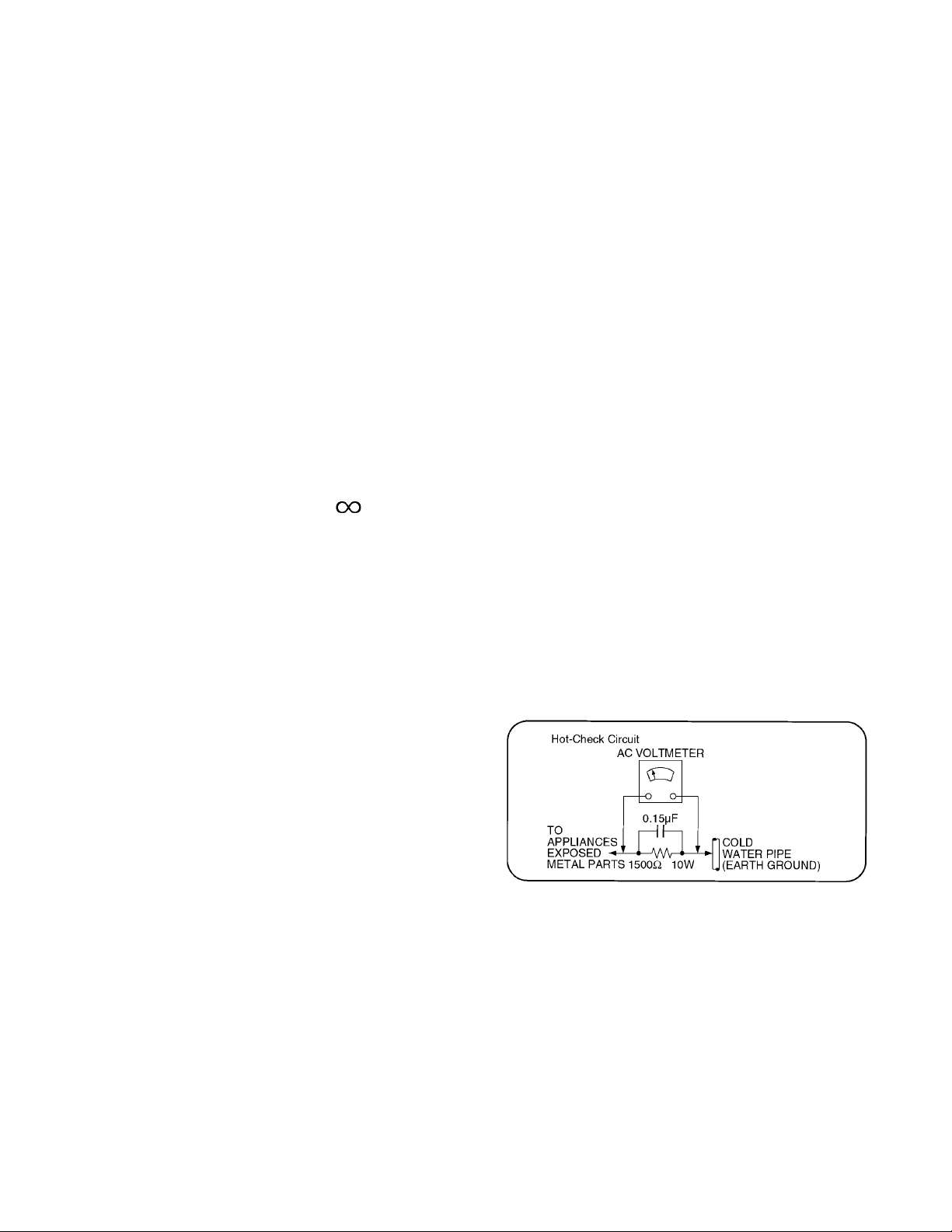
1.1.2. Leakage Current Hot Check (See Figure 1.)
1. Plug the AC cord directly into the AC outlet. Do not use
an isolation transformer for this check.
2. Connect a 1.5kohm, 10 watts resistor, in parallel with a
0.15μF capacitors, between each exposed metallic part
on the set and a good earth ground such as a water pipe,
as shown in Figure 1.
3. Use an AC voltmeter, with 1000 ohms/volt or more sensitivity, to measure the potential across the resistor.
4. Check each exposed metallic part, and measure the voltage at each point.
5. Reverse the AC plug in the AC outlet and repeat each of
the above measurements.
6. The potential at any point should not exceed 0.75 volts
RMS. A leakage current tester (Simpson Model 229 or
equivalent) may be used to make the hot checks, leakage
current must not exceed 1/2 milliamp. In case a measurement is outside of the limits specified, there is a possibility of a shock hazard, and the equipment should be
repaired and rechecked before it is returned to the customer.
Figure 1
3
Page 4

2 Warning
2.1. Prevention of Electrostatic Discharge (ESD) to Electrostatically Sensitive (ES) Devices
Some semiconductor (solid state) devices can be damaged easily by static electricity. Such components commonly are called Electrostatically Sensitive (ES) Devices. Examples of typical ES devices are integrated circuits and some field-effect transistors and
semiconductor [chip] components. The following techniques should be used to help reduce the incidence of component damage
caused by electrostatic discharge (ESD).
1. Immediately before handling any semiconductor component or semiconductor-equipped assembly, drain off any ESD on your
body by touching a known earth ground. Alternatively, obtain and wear a commercially available discharging ESD wrist strap,
which should be removed for potential shock reasons prior to applying power to the unit under test.
2. After removing an electrical assembly equipped with ES devices, place the assembly on a conductive surface such as aluminum foil, to prevent electrostatic charge buildup or exposure of the assembly.
3. Use only a grounded-tip soldering iron to solder or unsolder ES devices.
4. Use only an anti-static solder removal device. Some solder removal devices not classified as [anti-static (ESD protected)] can
generate electrical charge sufficient to damage ES devices.
5. Do not use freon-propelled chemicals. These can generate electrical charges sufficient to damage ES devices.
6. Do not remove a replacement ES device from its protective package until immediately before you are ready to install it. (Most
replacement ES devices are packaged with leads electrically shorted together by conductive foam, aluminum foil or comparable conductive material).
7. Immediately before removing the protective material from the leads of a replacement ES device, touch the protective material
to the chassis or circuit assembly into which the device will be installed.
Caution
Be sure no power is applied to the chassis or circuit, and observe all other safety precautions.
8. Minimize bodily motions when handling unpackaged replacement ES devices. (Otherwise ham less motion such as the brushing together of your clothes fabric or the lifting of your foot from a carpeted floor can generate static electricity (ESD) sufficient
to damage an ES device).
4
Page 5
2.2. About lead free solder (PbF)
Note: Lead is listed as (Pb) in the periodic table of elements.
In the information below, Pb will refer to Lead solder, and PbF will refer to Lead Free Solder.
The Lead Free Solder used in our manufacturing process and discussed below is (Sn+Ag+Cu).
That is Tin (Sn), Silver (Ag) and Copper (Cu) although other types are available.
This model uses Pb Free solder in it’s manufacture due to environmental conservation issues. For service and repair work, we’d
suggest the use of Pb free solder as well, although Pb solder may be used.
PCBs manufactured using lead free solder will have the PbF within a leaf Symbol PbF stamped on the back of PCB.
Caution
• Pb free solder has a higher melting point than standard solder. Typically the melting point is 50 ~ 70 °F (30~40 °C) higher. Please
use a high temperature soldering iron and set it to 700 ± 20 °F (37 0 ± 10 °C).
• Pb free solder will tend to splash when heated too high (about 1100 °F or 600 °C).
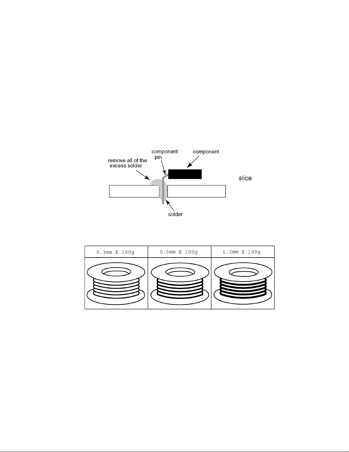
If you must use Pb solder, please completely remove all of the Pb free solder on the pins or solder area before applying Pb solder. If this is not practical, be sure to heat the Pb free solder until it melts, before applying Pb solder.
• After applying PbF solder to double layered boards, please check the component side for excess solder which may flow onto the
opposite side. (see figure below)
Suggested Pb free solder
There are several kinds of Pb free solder available for purchase. This product uses Sn+Ag+Cu (tin, silver, copper) solder. However, Sn+Cu (tin, copper), Sn+Zn+Bi (tin, zinc, bismuth) solder can also be used.
5
Page 6
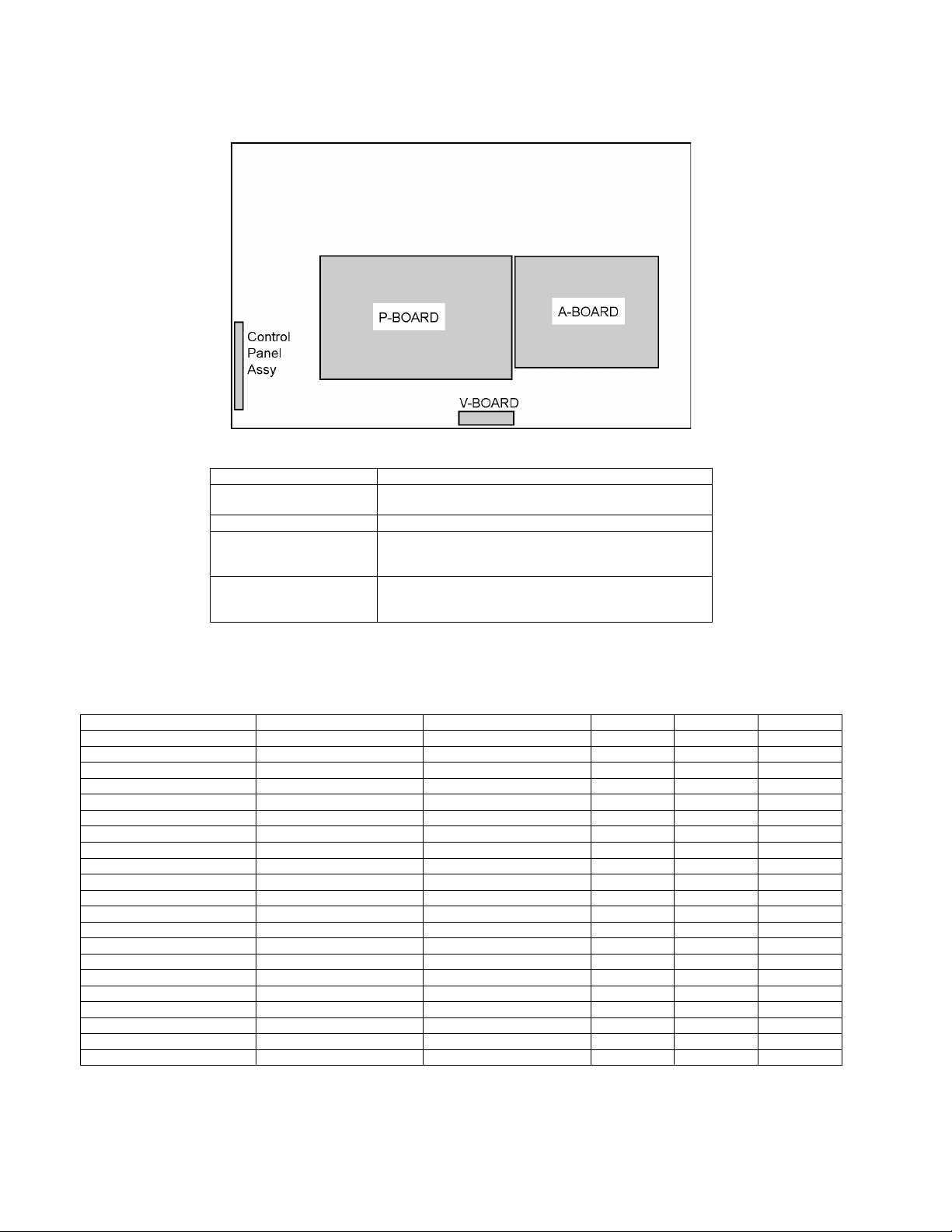
3 Service Navigation
3.1. Service Hint
Board Name Function
A-Board Rear Terminal, AV Switch, MCU, Audio & Video
V-Board Remote Receiver, LED
P-Board Power (AC/DC), DC-DC
Control Panel Assy Control Button, Power switch
Processor, LVDS, Tuner
Non-serviceable
P-Board should be exchanged for service.
Non-serviceable
Control Panel Assy should be exchanged for service.
3.2. Applicable signals
Input signal that can be displayed
* Mark: Applicable input signal for Component (Y, P
horizontal frequency (kHz) vertical frequency (Hz) COMPONENT HDMI PC
525 (480) / 60i 15.73 59.94 * *
525 (480) /60p 31.47 59.94 * *
750 (720) /60p 45.00 59.94 * *
1,125 (1,080) /60i 33.75 59.94 * *
640 × 400 @70 31.47 70.08 *
640 × 480 @60 31.47 59.94 *
Macintosh13 inch (640 × 480) 35.00 66.67 *
640 × 480 @75 37.50 75.00 *
852 × 480 @60 31.47 59.94 *
800 × 600 @60 37.88 60.32 *
800 × 600 @75 46.88 75.00 *
800 × 600 @85 53.67 85.08 *
Macintosh16 inch (832 × 624) 49.73 74.55 *
1,024 × 768 @60 48.36 60.00 *
1,024 × 768 @70 56.48 70.07 *
1,024 × 768 @75 60.02 75.03 *
1,024 × 768 @85 68.68 85.00 *
Macintosh 21 inch (1,152 × 870) 68.68 75.06 *
1,280 × 768 @60 47.70 60.00 *
1,280 × 1,024 @60 63.98 60.02 *
1,366 × 768 @60 48.36 60.00 *
Note:
• Signals other than above may not be displayed properly.
• The above signals are reformatted for optimal viewing on your display.
, PR), HDMI and PC
B
6
Page 7

4 Specifications
Power Source AC 110-127 V, 60 Hz
Power Consumption
Maximum 120 W
Standby Condition 0.7 W
Display panel
Aspect Ratio 16:9
Visible screen size 32 inch class (31.5 inches measured diagonally)
(W × H × Diagonal) 27.5 inch × 15.4 inch × 31.5 inch (698 mm × 392 mm × 800 mm)
(No. of pixels) 1,049,088 (1,366 (W) × 768 (H)) [4,098 × 768 dots]
Sound
Speaker 1-way 2 speakers slim under SP System
Audio Output 20 W [10 W + 10 W] ( 10 % THD )
PC signals VGA, SVGA, XGA, WXGA, SXGA
Channel CapabilityATSC/NTSC (Digital/Analog)
Operating Conditions Temperature: 32 °F - 95 °F (0 °C - 35°C)
Connection Terminals
VIDEO IN 1 VIDEO: RCA PIN Type × 1 1.0 V [p-p] (75 Ω)
VIDEO IN 2 VIDEO: RCA PIN Type × 1 1.0 V[p-p] (75 Ω)
COMPONENT IN 1 Y: 1.0 V [p-p] (including synchronization)
HDMI 1-2 TYPE A Connector × 2 .
PC D-SUB 15PIN: R,G,B / 0.7 V [p-p] (75 Ω)
Card slot SD CARD slot × 1
DIGITAL AUDIO OUT PCM / Dolby Digital, Fiber Optic
FEATURES CLO
Dimensions (W × H × D)
Including TV stand 31.5 inch × 21.7 inch × 8.6 inch (798 mm × 551 mm × 217 mm)
TV Set only 31.5 inch × 20.2 inch × 3.3 inch (798 mm × 511 mm × 83 mm)
Mass
Including TV stand 28.9 lb. (13.1 kg) NET
TV Set only 25.1 lb. (11.4 kg) NET
Horizontal scanning frequency 31 - 69 kHz
Vertical scanning frequency 59 - 86 Hz
VHF/ UHF: 2 - 69, CATV: 1 - 135
Humidity: 20 % - 80 % RH (non-condensing)
AUDIO L - R: RCA PIN Type × 2 0.5 V [rms]
S VIDEO: Mini DIN 4-pin Y: 1.0 V [p-p] (75 Ω) C: 0.286 V [p-p] (75 Ω)
AUDIO L - R: RCA PIN Type × 2 0.5 V [rms]
PB, PR: ±0.35 V [p-p]
AUDIO L-R: RCA PIN Type × 2 0.5 V [rms]
O This TV supports [HDAVI Control 4] function.
HD, VD / 1.0 - 5.0 V [p-p] (high impedance)
SED CAPTION, V-Chip
HDMI (HDAVI Control 4)
Vesa compatible, Photo viewer
Note
Design and Specifications are subject to change without notice. Mass and Dimensions shown are approximate.
7
Page 8
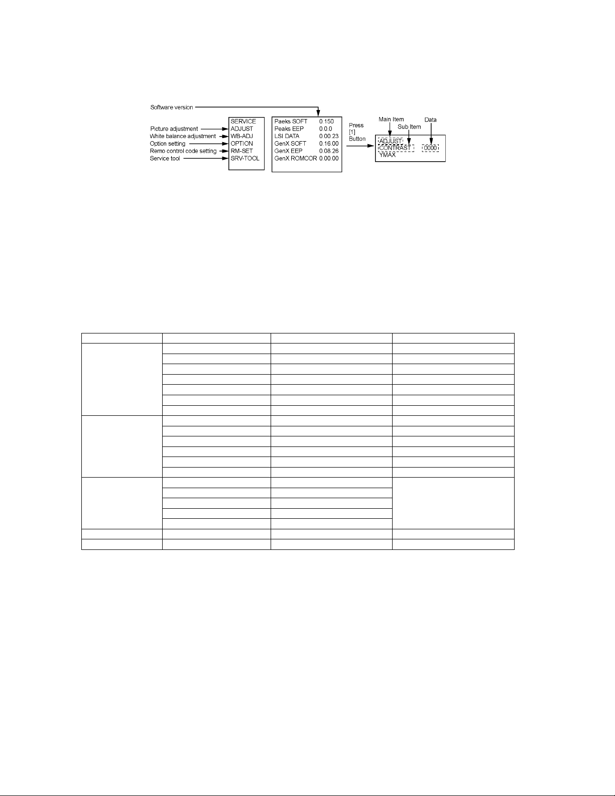
5 Service Mode
5.1. How to enter into Service Mode
While pressing [VOLUME ( - )] button of the main unit, press [INFO] button of the remote control three times within 2 seconds.
5.1.1. Key command
[1] button...Main items Selection in forward direction
[2] button...Main items Selection in reverse direction
[3] button...Sub items Selection in forward direction
[4] button...Sub items Selection in reverse direction
[VOL] button...Value of sub items change in forward direction ( + ), in reverse direction ( - )
5.1.2. Contents of adjustment mode
• Value is shown as a hexadecimal number.
• Preset value differs depending on models.
• After entering the adjustment mode, take note of the value in each item before starting adjustment.
Main item Sub item Sample Data Remark
ADJUST CONTRAST 000
COLOR 4C
TINT 00
SUB-BRT 808
BACKLGT 22E
B-Y-G 34
R-Y-A 00
WB-ADJ R-GAIN F7
G-GAIN FB
B-GAIN DB
R-CENT 82
G-CENT 80
B-CENT 86
OPTION Boot ROM Factory Preset.
STBY-SET 00
EMERGENCY ON
CLK MODE 00
CLOCK 0E4
RM-SET 00 Fixed.
SRV-TOOL 00 See next.
5.1.3. How to exit
Switch off the power with the [POWER] button on the main unit or the [POWER] button on the remote control.
8
Page 9
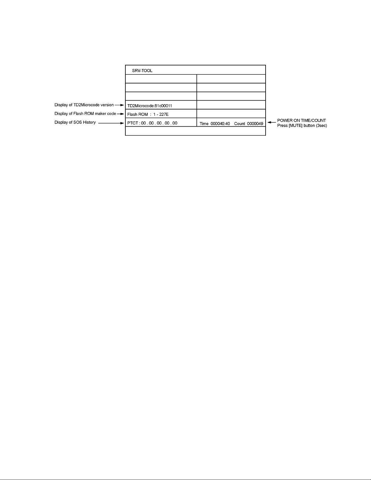
5.2. SRV-TOOL
5.2.1. How to access
1. Select [SRV-TOOL] in Service Mode.
2. Press [OK] button on the remote control.
5.2.2. Display of SOS History
SOS History (Number of LED blinking ) indication.
From left side; Last SOS, before Last, three occurrence before, 2nd occurrence after shipment, 1st occurrence after shipment.
This indication except 2nd and 1st occurrence after shipment will be cleared by [Self-check indication and forced to factory shipment setting].
5.2.3. POWER ON TIME/COUNT
Note : To display TIME/COUNT menu, highlight position, then press MUTE for 3sec.
Time : Cumulative power on time, indicated hour : minute by decimal
Count : Number of ON times by decimal
Note : This indication will not be cleared by either of the self-checks or any other command.
5.2.4. Exit
1. Disconnect the AC cord from wall outlet.
9
Page 10
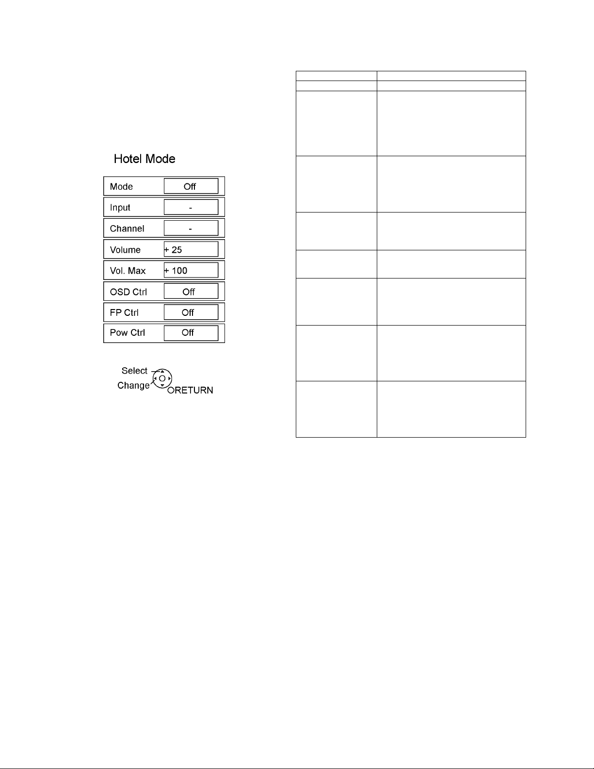
5.3. Hotel mode
1. Purpose
Restrict a function for hotels.
2. Access command to the Hotel mode setup menu
In order to display the Hotel mode setup menu, please
enter the following command (within 2 second).
[TV] : Vol. [Down] + [REMOTE] : INPUT (3 times)
Then, the Hotel mode setup menu is displayed.
3. To exit the Hotel mode setup menu
Disconnect AC power cord from wall outlet.
4. Explain the Hotel mode setup menu
item Function
Mode Select hotel mode off/on
Input Select input signal modes.
Set the input, when each time power is
switched on.
Selection:
-/RF/Component/HDMI1/HDMI2/Video1/
Video2/PC
• Off: give priority to a last memory.
Channel Select channel when input signal is RF.
Set the channel, each time power is switched
on.
Selection:
Any channel number or [-].
[-] means the channel when turns off.
Volume Adjust the volume when each time power is
switched on.
Range:
0 to 100
Vol. Max Adjust maximum volume.
Range:
0 to 100
OSD Ctrl Restrict the OSD.
Selection:
OFF/PATTERN1
• OFF: No restriction
• PATTERN1: restriction
FP Ctrl Select front key conditions.
Selection:
Off/Pattern1/All
• Off: altogether valid.
• Pattern1: only input key is valid.
• All: altogether invalid.
Pow Ctrl Select POWER-ON/OFF condition when AC
power cord is disconnected and then connected.
OFF: The same condition when AC power
cord is disconnected.
ON: Forced power ON condition.
10
Page 11
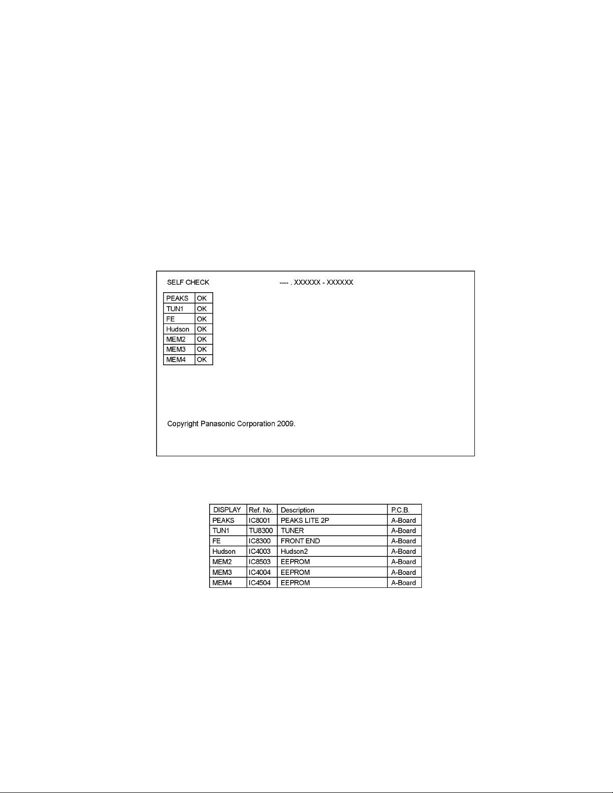
6 Troubleshooting Guide
Use the self-check function to test the unit.
1. Checking the IIC bus lines
2. Power LED Blinking timing
6.1. Check of the IIC bus lines
6.1.1. How to access
Self-check indication only:
Produce TV reception screen, and while pressing [VOLUME ( - )] button on the main unit, press [OK] button on the remote control
for more than 3 seconds.
Self-check indication and forced to factory shipment setting:
Produce TV reception screen, and while pressing [VOLUME ( - )] button on the main unit, press [MENU] button on the remote
control for more than 3 seconds.
6.1.2. Exit
Disconnect the AC cord from wall outlet.
6.1.3. Screen display
6.1.4. Check Point
Confirm the following parts if NG was displayed.
11
Page 12
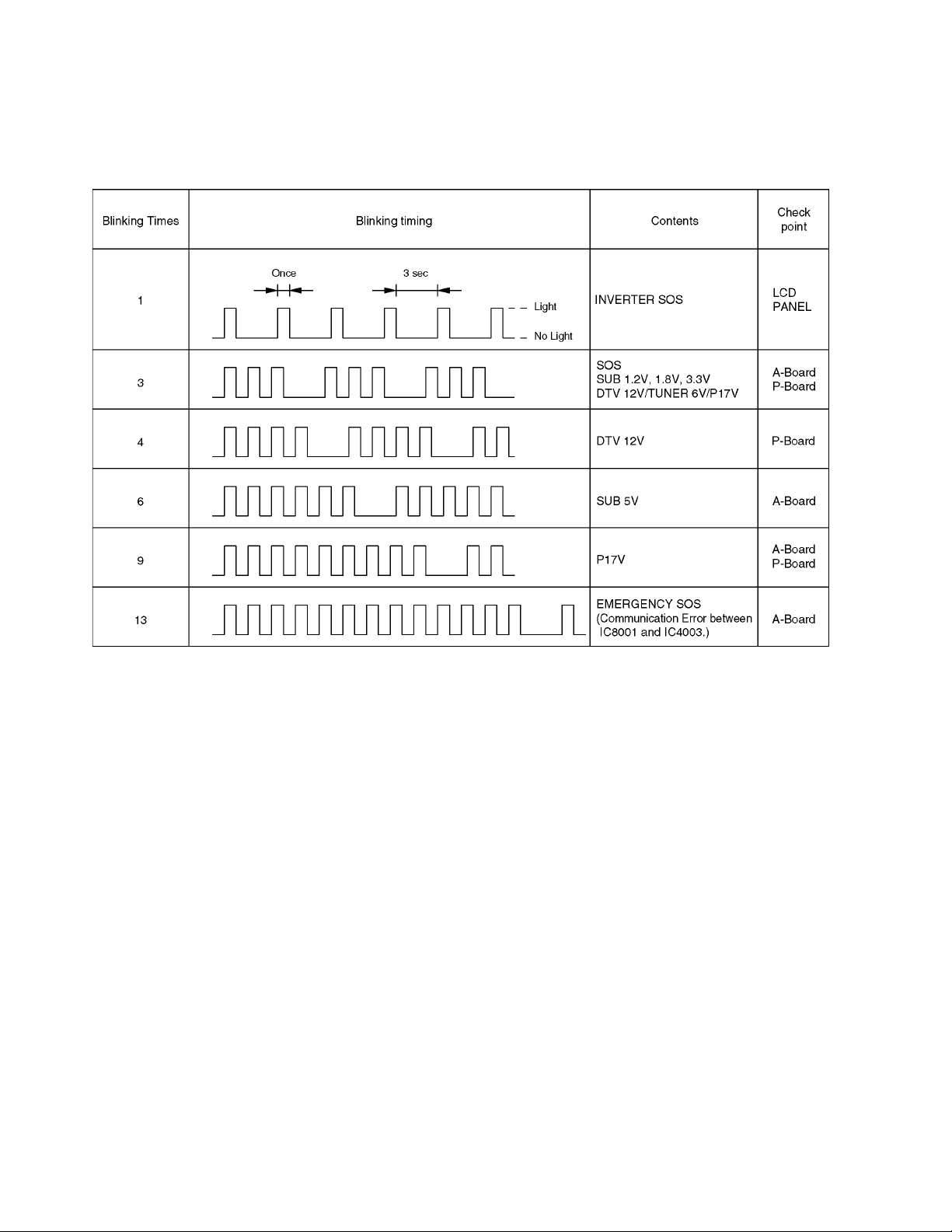
6.2. Power LED Blinking timing chart
1. Subject
Information of LED Flashing timing chart.
2. Contents
When an abnormality has occurred the unit, the protection circuit operates and reset to the stand by mode. At this time, the
defective block can be identified by the number of blinks of the Power LED on the front panel of the unit.
12
Page 13
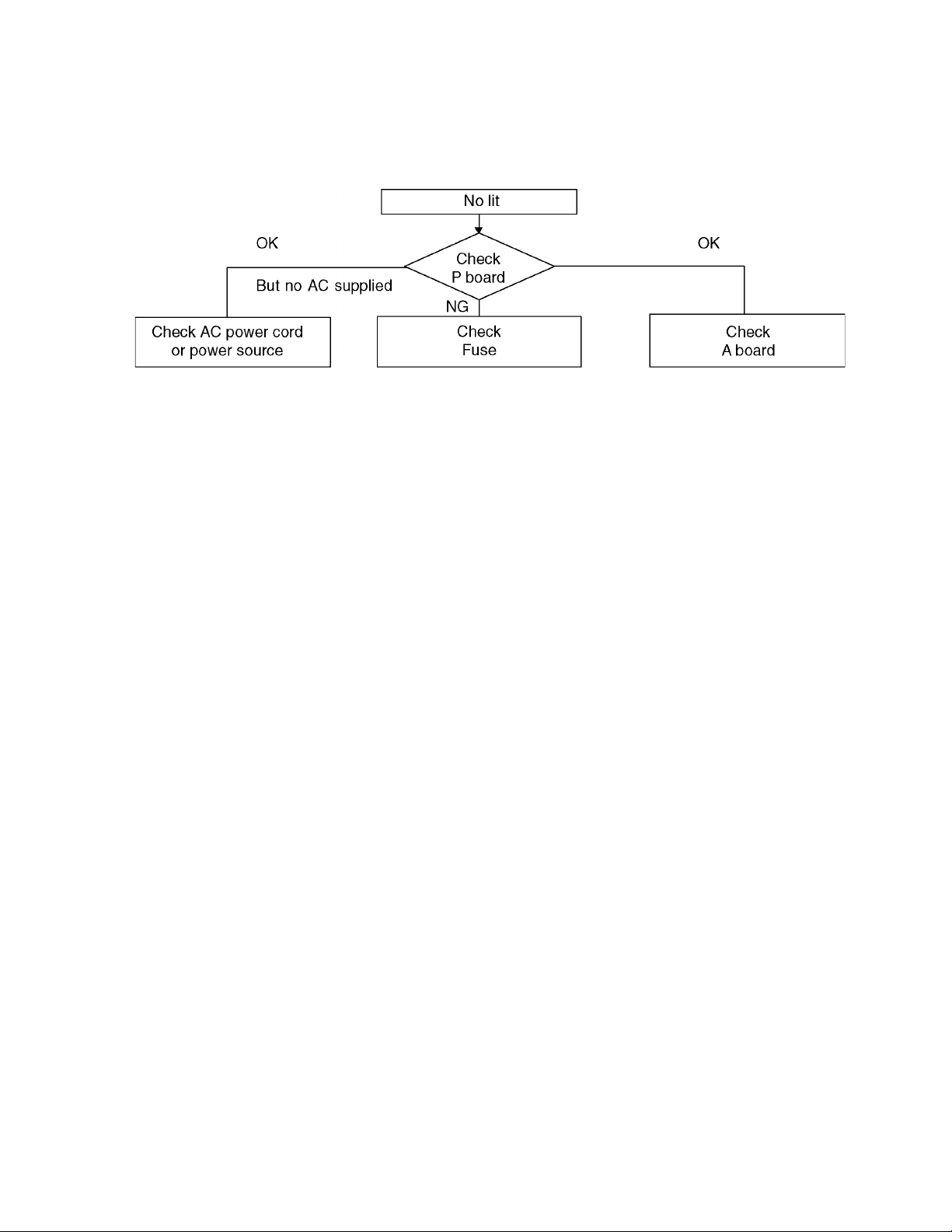
6.3. No Power
First check point
There are following 2 states of No Power indication by power LED.
1. No lit
2. Red is lit then turns red blinking a few seconds later. (See 6.2.)
13
Page 14
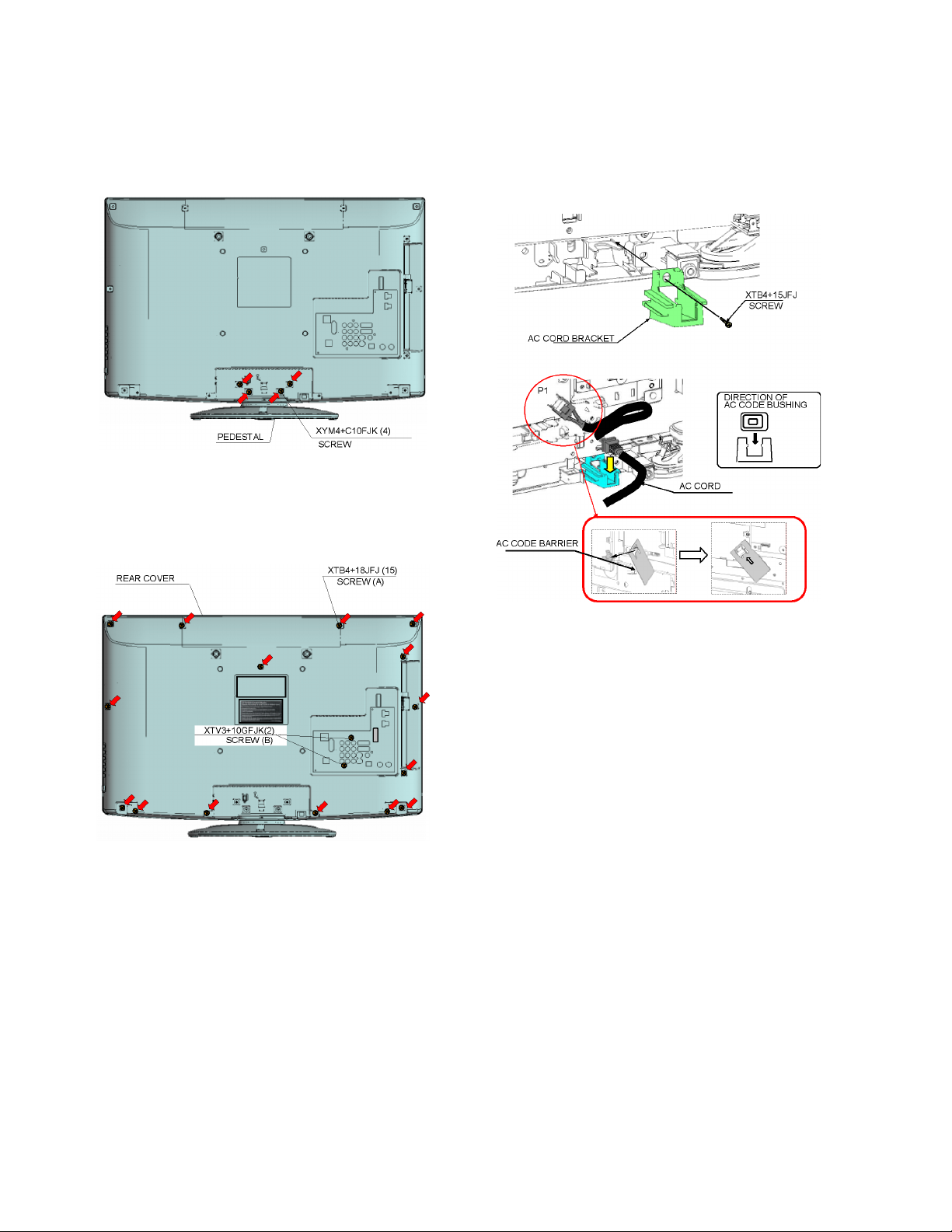
7 Disassembly and Assembly Instructions
7.1. Pedestal
1. Lay down the unit so that the rear cover faces upward.
2. Remove the 4 screws.
3. Remove the pedestal.
7.2. Rear cover
1. Remove the 15 screws (A).
2. Remove the 2 screws (B),
3. Remove the rear cover.
7.3. AC cord
1. Remove the screw and Remove the AC cord bracket.
2. Remove the bushing of the AC cord from the AC cord
bracket.
3. Disconnect the connector (P1) of AC cord.
14
Page 15
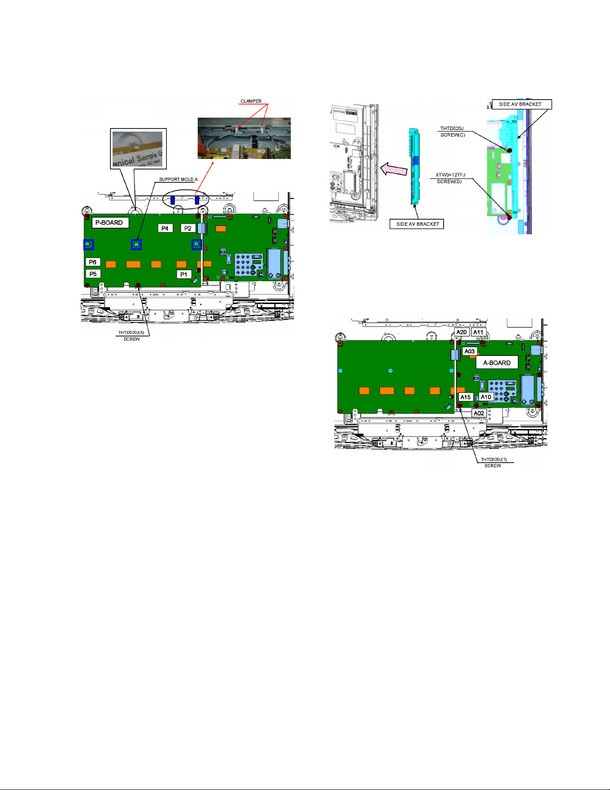
7.4. P-Board
1. Remove the 5 screws.
2. Disconnect the connectors (P1, P2, P3, P4, P5, P6).
3. Remove the P-Board.
7.5. Side AV bracket
1. Remove the 1 screw (C).
2. Remove the 1 screw (D).
3. Remove the side AV bracket.
7.6. A-Board
1. Remove the 7 screws.
2. Disconnect the connector (A02, A03, A10, A11, A15,
A20).
3. Remove the A-Board.
15
Page 16
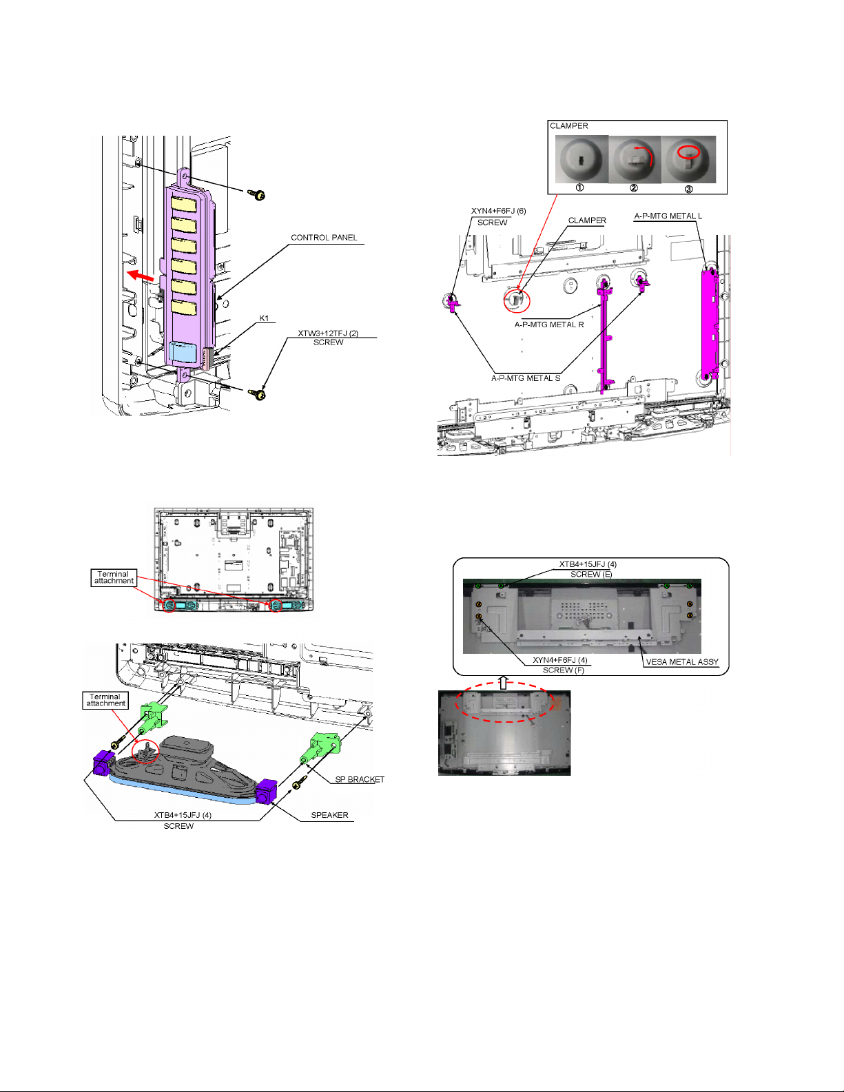
7.7. Control panel
1. Disconnect the connector (K1).
2. Remove the 2 screws.
3. Remove the control panel.
7.8. Speaker
1. Remove the 4 screws.
2. Remove the speaker.
7.9. A-P-MTG Metal
1. Remove the 6 screws.
2. Remove the A-P-MTG metal R/L/S.
7.10. VESA metal
1. Remove the 4 screws (E).
2. Remove the 4 screws (F).
3. Remove the VESA metal.
16
Page 17
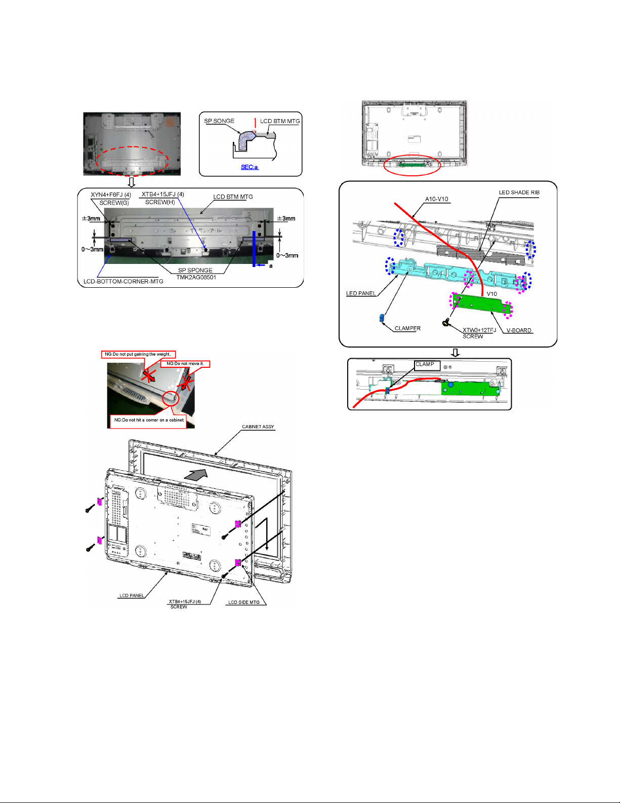
7.11. LCD MTG
1. Remove the 4 screws (G).
2. Remove the 4 screws (H).
3. Remove the LCD BTM MTG and LCD bottom corner
BTG.
7.12. LCD Panel
1. Remove the 4 screws.
2. Remove the LCD panel and LCD side MTG.
7.13. V-Board
1. Remove the 1 screw.
2. Disconnect the connector (V10).
3. Remove the V-Board.
17
Page 18
7.14. EMI processing
18
Page 19

192021
Page 20

Page 21

8 Measurements and Adjustments
8.1. Voltage chart of A-board
VOLTAGE TEST POINT SPECIFICATION
STB3.3V TP2843 3.3 ± 0.16 V
STB1.8V TP7006 1.84 ± 0.09 V
SUB1.2V TP5602 1.26 ± 0.06 V
SUB1.8V TP5601 1.84 ± 0.09 V
SUB3.3V TP5600 3.3 ± 0.16 V
SUB5V TP5405 5 ± 0.25 V
SUB9V TP5481 9 ± 0.45 V
BT30V TP8300 30 ± 1.5 V
SOUND17V TP5431 17 ± 0.85 V
DTV12V TP5432 12 ± 0.6 V
PANEL12V TP5413 12 ± 0.6 V
5VS TP5433 5.7 ± 0.28 V
TUNER6V TP5439 5.7 ± 0.28 V
(Reception state)
8.2. Picture level adjustment (RF)
Instrument Name Remarks
1. REMOTE TRANSMITTER
2. Ex. Signal (Sprit color bar)
Adjustment or Inspection Procedure Remarks
<procedure>
1. Receive the Sprit color bar.
(Screen mode: ZOOM or FULL Picture mode: DYNAMIC AI: OFF AI Picture: OFF)
*BACK LIGHT +30
<Inspection>
1. Enter Service mode, and select MAIN_ADJ PICTURE.
Volume UP/DOWN key makes GAIN displayed under PICTURE to set.
Pushing the remote controller [OK] key for about 3 seconds, GAIN is suited
to the adjustment value automatically.
(The Sprit Color Bar Pattern)
Page 22

8.3. Picture level adjustment (VIDEO)
Instrument Name Remarks
1. REMOTE TRANSMITTER
2. Video signal generator (100% Color bar)
Adjustment or Inspection Procedure Remarks
<procedure>
1. Receive 100% Color bar.
(ASPECT: ZOOM or FULL, Picture mode: VIVID, AI Picture: OFF)
* BACK LIGHT MAX VALUE
<Inspection>
1. Enter Service mode, and select ADJUST CONTRAST.
Volume UP/DOWN key makes GAIN value displayed on the right of CONTRAST to set.
Pushing the remote controller [OK] key for about 3 seconds, GAIN is suited to the adjustment value automatically.
8.4. Picture level adjustment (YUV)
Instrument Name Remarks
1. REMOTE TRANSMITTER
2. Component Video signal generator (100% Color bar 1080i)
Adjustment or Inspection Procedure Remarks
<procedure>
1. Receive 100% Color bar.
(ASPECT: ZOOM or FULL, Picture mode: VIVID, AI Picture: OFF)
* BACK LIGHT MAX VALUE
<Inspection>
1. Enter Service mode, and select ADJUST CONTRAST.
Volume UP/DOWN key makes GAIN value displayed on the right of CONTRAST to set.
Pushing the remote controller [OK] key for about 3 seconds, GAIN is suited to the adjustment value automatically.
22
Page 23

(LED:4 TIMES)
(LED:6 TIMES)
(LED:9 TIMES)
(LED:1 TIME)
(LED:3 TIME)
(LED:4 TIMES)
(LED:6 TIMES)
(LED:9 TIMES)
(LED:1 TIME)
(LED:3 TIME)
+1.8V
EEPWP
EEPROM
IIC3
INV SOS
A07
SWICH
SD CARD
HDMI1
SPDIF
SUB+3.3V
DDR2 SDRAM
CLOCK
GEN
SUB_ON
27MHz
74MHz
27MHz
Peaks Lite2p
SUB+1.2V
FLASH
MEMORY
V10
PANEL
REMOTE
STB+1.8V
TS Serial
DCDC
SPEAKER
(L,R)
STB+5V
VIDEO2
MODULE P
FOR
FACTORY
USE
A15
SERIAL
TV-L,R
PANEL
PANEL+12V
A10
DTV+12V
AC CORD
A03
SBO2
SBI2
VIDEO1
P5
V
Digital/Analog
Tuner
KEY SCAN
A11
OPT OUT
L,R
LVDS
Y,PB,PR
STB+3.3V
BACK LIGHT
CONTROL
L,R
RESET
A02
DTV Audio signal
SUB+5V
DTV12V SENSE
+3.3V
REMOTE
STB+5V
TS Serial
Video front-end,
Audio processor,
Micom,
HDMI-Receiver
AUDIO AMP
SUB+3.3V
COMP1
HUNSON2
SUB+1.8V
DCDC
SUB+1.2V
A12
SUB+1.8V
Digital Video signal
V,Y,C
SUB+3.3V
L,R
DTV+12V
PWM
SEL
FOR
FACTORY
USE
HDMI2
Control
Panel
Assy
A20
SOUND SOS
LED
DCDC
EEPROM
L,R
INV SOS
STB+3.3V
P2
SOS
SD CARD I/F
A-BOARD
SUB5V SENSE
RESET
SPDIF
LED
REMOTE
CONTROL
LED
(MAIN MCU+VIDEO SIGNAL PROCESSOR)
P1
*IP CONVERTER
SD BOOT
*SCALING
TV-V
*OSD MIX
V
DCDC
*PICTURE CORRECT
FRONT END
IFD1/2
V-BOARD
K1
LCD PANEL
PC
R,G,B
FOR
FACTORY
USE
A06
17V
TUNER6V
DTV12V
STB5V
SUB_ON
OVP_DET
P4
P6
9 Block Diagram
9.1. Main Block Diagram
23
Page 24

9.2. Block (1/2) Diagram
(LED:4 TIMES)
(LED:6 TIMES)
(LED:9 TIMES)
(LED:1 TIME)
(LED:3 TIME)
JK4500
HDMI1
JK4501
HDMI2
JK4800
VIDEO2
JK3001
VIDEO1
COMPNENT
ANT IN
A-BOARD
V2_Y
V2_C
S
V2_V
V
V2_L
L
V2_R
R
V1_V
V
V1_L
L
V1_R
R
D1_Y
Y
D1_PB
PB
D1_PR
PR
D1_L
L
D1_R
R
+5V
CEC
DDC IIC1
+5V
CEC
DDC IIC2
TU8300
Digital/Analog
Tuner
TV_V
RF_L/R
IFD1/2
IF AGC
SUB+5V
BT_30V
JK3104
PC IN
Q4503
5V DET1
Q4502
5V DET2
IIC
HDMI_5V_DET1
HDMI_5V_DET2
HDMI_CEC
IC8300
FRONT END
DIGITAL
DEMODULE
SUB3.3V
SUB1.2V
IIC2
HDMI MULTIPLEXR
DDC IIC1
HDMI1
DDC IIC2
HDMI2
CH0 DATA,CLK,SYNC
IC4503
EEPROM
IC4500
DDC IIC0
+3.3V
HDMI
EEPROM
IC4501
+5V
IC4506
+3.3V
HDMI_5V_DET1
HDMI_5V_DET2
HDMI_5V_DET3
HDMI_CEC
V-BOARD
D2500A
POWER LED
1
OUT
RM2500
REMOCON
2
GND
3
VCC
Control Panel Assy
SUB5V
V10
3
1
2
K1
1
3
REMOTE
R_LED_ON
STB 3.3V
KEY1
KEY3
BRG
IIC
IIC1
IIC2
IIC3
A10
3
1
2
A02
1
3
IC4003
Video front-end,
Audio processor,
Micom,HDMI-Receiver
PCRGB
DDC IIC0
HDMI
V/Y/C
VIDEO2
L/R
V
VIDEO1
L/R
Y/PB/PR
COMP
L/R
V
L/R
IC5481
BT+30V
+30V
Hundson2
TV
SOUND_SOS
(LED:9 TIMES)
DTV12V_SENSE
(LED:4 TIMES)
SUB5V_SENSE
(LED:6 TIMES)
SBO2,SBI2
(LED:3 TIME)
(LED:1 TIME)
IC5409
SUB+9V
+9V
IC3202
AMP
STB1.8V
SUB_ON
INV_SOS
STB3.3V
RESET
IC7005
STB+1.8V
STB5V
+1.8V
2
3
Analog Audio signal
OPT.Audio out
IC4001
4
5
RESET
Digital Video signal
Digital Audio signal
SERIAL
SOS
Analog ASIC
TV SOS
SOS SENSE
SUB_ON
DCDC_CTL
IC4004
EEPROM
IC4504
HDCP
EEPROM
IC5480
OVP
D5619
D5613
D5627
RESET
+3.3V
Peaks_RESET
PANEL_ON
IIC
IIC
D5618
D5612
D5626
IC4005
FLASH
MEMORY
R_LED_ON
R_LED_ON
RMIN
KEY1
KEY3
RMIN
KEY1
KEY3
D5711
6
7
8
9
10
11
12
13
14
15
P1
2
AC CORD
MODULE P
1
INV_ON
ADIM
INV_PWM
INV_SOS
A03
23
5
Q5433
3
22
20
13
12
16
17
19
A20
3
2
4
5
DTV12V
TUNER6V
P17V
D5713
D5715
D7084
D5714
D5716
D7085
IC5405
+5V
SUB_5V
DTV12V
SUB+3.3V
+3.3V
IC5600
IC5601
SUB3.3V
+1.2V
+1.8V
SUB1.2V
SUB1.8V
16
17
18
19
P2
23
STB5V
5
SUB_ON
3
RELAY
22
TUNER6V
20
TUNER6V
13
17V
12
17V
16
DTV12V
17
DTV12V
19
DTV12V
P4
3
2
4
5
1
1
P5
22
P6
24
Page 25

INV_PWM
ADIM
INV_SOS
INV_ON
SUB3.3V
SUB1.8V
SUB3.3V
SUB3.3V
P17V
D3050
IC8001
Peaks-Lite2p
SUB1.2V
SUB1.8V
2
4
SD CARD SLOT
SUB3.3V
IC8002
CONTROL
PANEL_SOS
DDR2 SDRAM
PANEL
DDR2 I/F
LCD PANEL
CLOCK GEN
74MHz
IC8004
7
FLASH
MEMORY
IC8502
IIC2
EEPROM
IIC1
IC8503
IIC3
SBO2
SBI2
SD I/F
JK8302
SPEAKER(L)
R(-)
PWM
CONTROL
OPT.Audio out
PANEL+12V
LVDS
28
30
PANEL
BACK LIGHT
A11
20
A12
FOR
FACTORY
USE
31
(MAIN MCU+VIDEO SIGNAL PROCESSOR)
FOR
FACTORY
USE
27MHz
A07
Control voltage
CH0 TS Serial
SPDIF
Digital Video signal
L(+)
A15
AUDIO AMP
SPEAKER
OUT
1
3
LVDS I/F
SPEAKER(R)
SERIAL I/F
IC2301
R(+)
L(-)
SOS
Digital Audio signal
+17V
IC4007
SEL
HDMI_OPT_ENB
A-BOARD
29
Q5412
XRST
CPU BUS I/F
SD DATA
A06
FOR
FACTORY
USE
IIC2
IIC1
IIC3
INV_ON
PWMA
PWMK
17
19
18
13
14
11
12
10
15
16
7
8
2
6
4
9
3
5
9.3. Block (2/2) Diagram
25
Page 26

26
Page 27

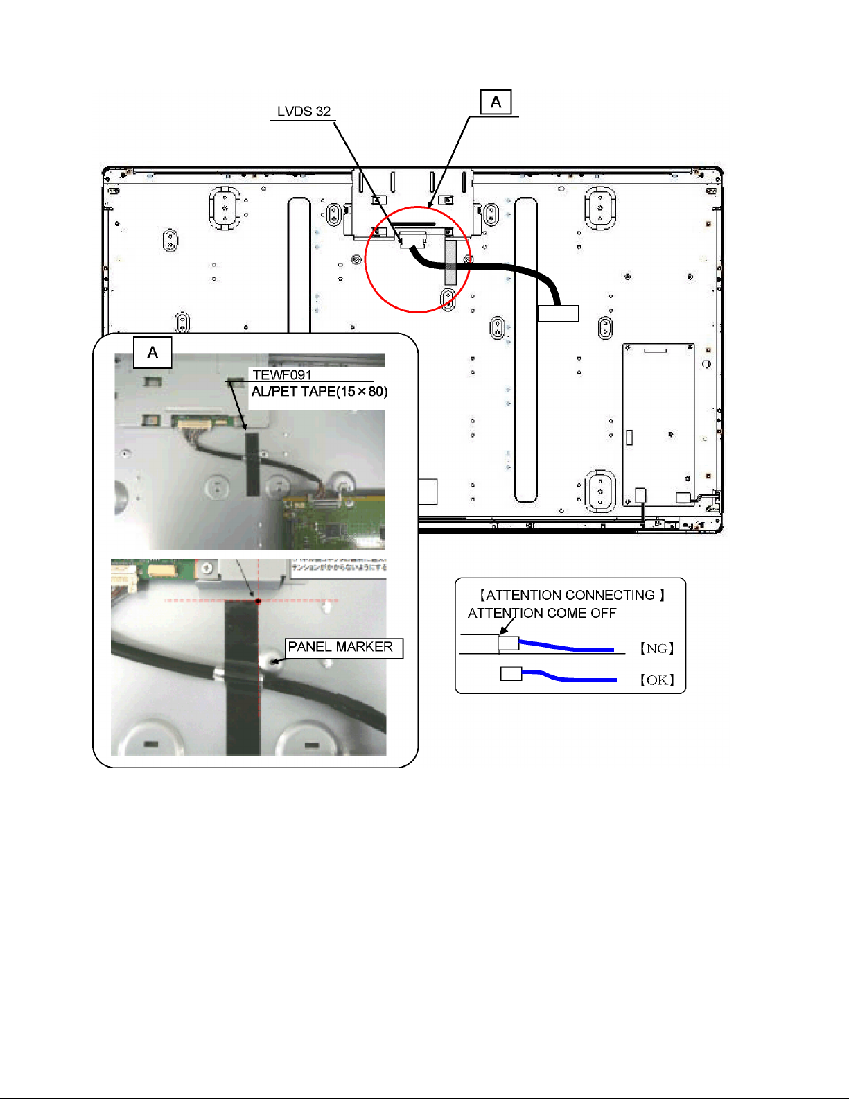
10 Wiring Connection Diagram
10.1. Caution statement.
Caution:
Please confirm that all flexible cables are assembled correctly.
Also make sure that they are locked in the connectors.
Verify by giving the flexible cables a very slight pull.
10.2. Wiring
27
Page 28

28
Page 29

11 Schematic Diagram
11.1. Schematic Diagram Notes
29
Page 30

11.2. A-Board (1/10) Schematic Diagram
IC8001
MN2WS0047
Peaks-Lite2
A
B
C
LOSD OUT (for HQ1)
LVDS I/F
TO 6/10
R8108
33k
C8069
50V
82p
C8067
16V
0.01u
IC8001 C15 VOP21
IC8001 E16 VOP20
IC8001 F16 VOP11
IC8001 A16 VOP10
IC8001 C16 VOP1
IC8001 B16 VOP0
IC8001 B15 LCSID
IC8001 A15 LCSCK
IC8001 E11 VI1CVBS3
IC8001 E10 VI1CVBS2
IC8001 F10 VI1CVBS1
IC8001 E9 VI1CVBS0
IC8001 F9 VI1CK204F
IC8001 E8 VI1CK208F
IC8001 F8 VI2P0
IC8001 E7 VI2P1
IC8001 F7 VI2P2
IC8001 D6 VI2P3
IC8001 D5 VI2P5
IC8001 F5 VI2P6
IC8001 E4 VI2P7
IC8001 D3 VI2P8
IC8001 F4 VI2P9
TCLK1N
IC8001 E25 TCLK1N
TA1N
IC8001 B25 TA1N
TB1N
IC8001 C25 TB1N
TC1N
IC8001 D25 TC1N
TD1N
IC8001 F25 TD1N
IC8001 G25 TE1N
TCLK1P
IC8001 E26 TCLK1P
TA1P
IC8001 B26 TA1P
IC8001 C26 TB1P
IC8001 D26 TC1P
TC1P
TD1P
IC8001 F26 TD1P
IC8001 G26 TE1P
R8106
2k
IC8001 G22 LPFOUT
IC8001 G23 LPFIN
R8107
100
C8068
16V
0.1u
LOSDOUT11
LOSDOUT10
LOSDOUT13
LOSDOUT12
LOSDOUT15
LOSDOUT14
LOSDOUT9
LOSDOUT8
LOSDOUT7
LOSDOUT6
LOSDOUT5
LOSDOUT4
LOSDOUT3
LOSDOUT2
LOSDOUT1
LOSDOUT0
LOSDOUT_CLK_O
LOSDOUT_H_O
LOSDOUT_YS
LOSDOUT_YM
LOSDOUT_V_I
LOSDOUT_CLK_I
LOSDOUT_H_I
AUDIO IF
TO 7/10
IC8001 D15 DAUDIO
DMIX0
IC8001 A13 DMIX0
SRCK0
IC8001 B13 SRCK0
LRCK0
IC8001 F14 LRCK0
IC8001 C13 DACCK0
TO 5/10
IECOUT0
IC8001 A10 IECOUT0
R8001
220
IC8001 R5 ATCPOUT
IC8001 P5 AVCOIN
R8002
56
C8002
C8072
0.1u
16V
C8073
0.1u
16V
C8074
0.1u
16V
C8070
0.1u
SUB3.3V
SUB3.3V
16V
C8001
16V
0.1u
L8009
J0JHC0000045
IC8001 P16 DPAVDD
IC8001 R16 N.C.(DPAVSS)
IC8001 H21 MVAVDD
IC8001 J21 MVAVSS
IC8001 P3 AGAVDD
IC8001 P2 AGAVSS
L8008
J0JHC0000045
C8071
16V
0.1u
IC8001 E22 LVVDD
IC8001 E23 LVVDD
IC8001 F21 LVVDD
6.3V
1u
SUB1.2V
L8004
J0JHC0000045
C8007
16V
0.1u
C8008
16V
0.1u
C8010
10V
10u
C8006
16V
0.1u
C8009
10V
10u
SUB3.3V
P
L8006
C8033
C8034
16V
16V
0.1u
0.1u
D
E
FOR HQ1L VIDEO
TO 6/10
SUB3.3V
IC8001 N17 VDDR
IC8001 R17 VDDR
IC8001 T15 VDDR
IC8001 U16 VDDR
IC8001 AB15 VDDR
IC8001 AC15 VDDR
IC8001 AD15 VDDR
IC8001 AE15 VDDR
IC8001 AF15 VDDR
IC8001 U14 N.C.(DPAVDD12)
IC8001 M17 VDDA
IC8001 U15 VDDA
IC8001 T17 VDDA
IC8001 F22 LVVSS
IC8001 F23 LVVSS
IC8001 G21 LVVSS
IC8001 C12 DACVDD1
IC8001 E14 DACVDD2
IC8001 C11 DACVSS1
IC8001 A12 DACVSS2
MVCLK
MHSYNC
VOP4
VOP3
R8773
IC8001
IC8001 C22 MHSYNC
IC8001 E20 MVSYNC
IC8001 E18 VOP29
IC8001 B18 VOP28
IC8001 F17 VOP27
IC8001 A18 VOP26
IC8001 C17 VOP25
IC8001 B17 VOP24
IC8001 A17 VOP23
IC8001 E17 VOP22
IC8001 B20 VOP19
IC8001 E19 VOP18
IC8001 A20 VOP17
IC8001 C19 VOP16
IC8001 F18 VOP15
IC8001 B19 VOP14
IC8001 A19 VOP13
IC8001 C18 VOP12
IC8001 B22 VOP9
IC8001 D20 VOP8
IC8001 A22 VOP7
IC8001 C21 VOP6
IC8001 F19 VOP5
IC8001 B21 VOP4
IC8001 A21 VOP3
IC8001 C20 VOP2
10k
IC8001 H26 VOUTENB
IIC I/F
TO 2,5/10
SCL0TB1P
SDA0
TO 2/10
SCL1
SDA1
SBT0
SBT2
XECS3
XECS5
SD CARD I/F
TO 2/10
SDCLK
SDCD
SDCMD
SDDAT0
SDDAT1
SDDAT2
SDDAT3
SDWP
1.8V_DDRI/F
C8011
16V
0.1u
C8012
16V
0.1u
C8013
16V
0.1u
C8014
16V
0.1u
C8015
6.3V 1u
C8016
6.3V
1u
C8017
10V
10u
C8077
16V
0.1u
C8078
16V
0.1u
C8079
16V
0.1u
C8080
16V
0.1u
A23 MVCLK
IC8001 M2 SCL0
IC8001 M1 SDA0
IC8001 N5 SCL1
IC8001 N3 SDA1
IC8001 AB8 SBT0
IC8001 AD6 SBT2
IC8001 AD1 XECS3
IC8001 AC4 XECS5
SUB1.8V
SDA2
SCL2
SDA3
SCL3
IC8001 AF13 SDCLK
IC8001 AD13 SDCD
IC8001 AD12 SDCMD
IC8001 AB12 SDDAT0
IC8001 AE13 SDDAT1
IC8001 AB13 SDDAT2
IC8001 AA13 SDDAT3
IC8001 AE12 SDWP
L8003
J0JHC0000045
IC8001 K23 VDDIO
IC8001 K26 VDDIO
IC8001 M21 VDDIO
IC8001 M23 VDDIO
IC8001 N24 VDDIO
IC8001 P25 VDDIO
IC8001 R21 VDDIO
IC8001 T25 VDDIO
IC8001 U24 VDDIO
IC8001 V22 VDDIO
IC8001 W26 VDDIO
IC8001 Y22 VDDIOCK IC8001AD20MMDQ19
IC8001 Y24 VDDIO
IC8001 AA21 VDDIO
IC8001 AB19 VDDIO
IC8001 AB22 VDDIO
IC8001 AB25 VDDIO
IC8001 AC18 VDDIO
IC8001 AC23 VDDIO
IC8001 AD17 VDDIO
IC8001 AD22 VDDIO
IC8001 AD25 VDDIO
IC8001 AE16 VDDIO
IC8001 AE21 VDDIO
IC8001 AF20 VDDIO
IC8001 AF26 VDDIO
DDR2
IC8002
C3ABSY000036
CH0DM0
CH0DM1
CH0DQS0
CH0DQS1
CH0DQ5
CH0DQ7
CH0DQ1
CH0DQ3
CH0DQ2
CH0DQ0
CH0DQ6
CH0DQ4
CH0DQ8
CH0DQ11
CH0DQ12
CH0DQ15
CH0DQ14
CH0DQ13
CH0DQ10
CH0DQ9
CH0ODT
R8074
220
CH0CK
CH0XCK
CH0CKE
CH0BA0
CH0BA1
CH0BA2
CH0XWE
CH0XRAS
CH0XCAS
CH0XCS0
CH0ODT
R8101
10k
CH0CKE
R8081
10k
R8097
220
CH0CK
CH0XCK
1.8V_DDRI/F
R8031
270
1%
R8035
S
R8032
270
1%
!
A-BOARD (1/10)
TXN/A10NGSS
IC8002 B3 UDM
IC8002 F3 LDM
IC8002 A8 UDQSIC8001 E1 VI1P11
IC8002 B7 UDQS
IC8002 E8 LDQS
IC8002 F7 LDQS
IC8002
B9 DQ15
IC8002 B1 DQ14
IC8002 D9 DQ13
IC8002 D1 DQ12
IC8002 D3 DQ11
IC8002 D7 DQ10
IC8002 C2 DQ9
IC8002 C8 DQ8
IC8002 F9 DQ7
IC8002 F1 DQ6
IC8002 H9 DQ5
IC8002 H1 DQ4
IC8002 H3 DQ3
IC8002 H7 DQ2
IC8002 G2 DQ1
IC8002 G8 DQ0
IC8002 K9 ODT
IC8002 J8 CK
IC8002 K8 CK
IC8002 K2 CKE
IC8002 L2 BA0
IC8002 L3 BA1
IC8002 L1 NC
K3 WE
IC8002
IC8002 K7 RAS
IC8002 L7 CAS
IC8002 L8 CS
IC8002 J2 VREF
C8040
16V
0.1u
C8041
16V
0.1u
C8042
C8043
10V
16V
16V
16V
68u
16V
0.1u
C8035
C8044
C8049
C8050
1.8V_DDRI/F
C8046
16V
0.1u
+
4V
C8047
16V
0.1u
C8048
16V
0.1u
C8036
10V
10u
10u
0.1u
0.1u
0.1u
IC8002
A1 VDD
IC8002 E1 VDD
IC8002 M9 VDD
IC8002 J9 VDD
IC8002 R1 VDD
IC8002 J1 VDDL
IC8002 A9 VDDQ
IC8002 C1 VDDQ
IC8002 C3 VDDQ
IC8002 C7 VDDQ
IC8002 C9 VDDQ
IC8002
E9 VDDQ
IC8002 G1 VDDQ
IC8002 G3 VDDQ
IC8002 G7 VDDQ
IC8002 G9 VDDQ
CH0A0
CH0A1
CH0A2
CH0A3
CH0A4
CH0A5
CH0A6
CH0A7
CH0A8
CH0A9
CH0A10
CH0A11
CH0A12
C8045
16V
0.1u
IC8002 A3 VSS
IC8002 E3 VSS
IC8002 J3 VSS
IC8002 N1 VSS
IC8002 P9 VSS
IC8002 A7 VSSQ
IC8002 B2 VSSQ
IC8002 B8 VSSQ
IC8002 D2 VSSQ
IC8002 D8 VSSQ
IC8002 E7 VSSQ
IC8002 F8 VSSQ
IC8002 H2 VSSQ
IC8002 H8 VSSQ
IC8002 J7 VSSDL
IC8002 A2 NC
IC8002 R3 NC
IC8002 R7 NC
IC8002 R8 NC
IC8002 M8 A0
IC8002 M3 A1
IC8002 M7 A2
IC8002 N2 A3
IC8002 N8 A4
IC8002 N3 A5
IC8002 N7 A6
IC8002 P2 A7
IC8002 P8 A8
IC8002 P3 A9
IC8002 M2 A10
IC8002 P7 A11
IC8002 R2 A12
SUB3.3V
R8772
10k
SUB3.3V
R8770
10k
SUB3.3V
R8604
10k
R8599
47k
CH,IS IF
TO 9/10
TO 6/10
TO 10/10
CLOCK GEN
CPU BUS I/F
TO 2/10
TO 9/10
TO 3/10
CH0CLK
CH0VAL
CH0PSYNC
CH0DATA
IS0DATA
IS1DATA
IC8001J22VC27
IC8001H25CLK74
IC8001K21CK27
IC8001AD24CK27D
EA0
IC8001 T1 EA0
EA1
IC8001 T2 EA1
EA2
IC8001 T6 EA2
EA3
IC8001 T3 EA3
EA4
IC8001 U4 EA4
EA5
IC8001 U1 EA5
EA6
IC8001 U2 EA6
EA7
IC8001
ED0
IC8001 U5 ED0
ED1
IC8001 V1 ED1
ED2VI1P24
IC8001 V2 ED2
ED3
IC8001 V5 ED3
ED4
IC8001 V3 ED4
ED5
IC8001 W1 ED5
ED6
IC8001 W2 ED6
ED7
IC8001 V6 ED7
ED8
IC8001 W3 ED8
ED9
IC8001 W4 ED9
IC8001 Y1 ED10
ED10
ED11
IC8001 Y2 ED11
ED12
IC8001 W5 ED12
IC8001 Y3 ED13
ED13
ED14
IC8001 AA1 ED14
ED15
IC8001 AA2 ED15
XERE
IC8001 Y4 XERE
XEWE0
IC8001 AA3 XEWE0
IC8001 AB3 XEWE1
IC8001 Y5 XEDK
IC8001 AB2 ERXW
IC8001 AB1 ECLK
IC8001 AA4 ESZ0
IC8001 AC1 ESZ1
XECS0
IC8001 AA5 XECS0
IC8001 AC2 XECS1
XECS4
IC8001 AC3 XECS4
XECS2
IC8001 AB4 XECS2
IC8001 N2 XNMIRQ
IC8001 N4 XIRQ1
XIRQ2
IC8001 N1 XIRQ2
IC8001 P1 XIRQ3
IC8001 AF23 BOOTSWAP
XRST
IC8001 D21 XRST
IC8001 AF12 CH0CLK
IC8001 AE11 CH0VAL
IC8001 AD11 CH0PSYNC
IC8001 AF11 CH0DATA
IC8001 AF3 IS0CLK
IC8001 AB7 IS0VAL
IC8001 AE4 IS0PSYNC
IC8001 AF4 IS0DATA
IC8001 AE5 IS1VAL
IC8001 AC7 IS1PSYNC
IC8001 AD5 IS1CLK
IC8001 AF5 IS1DATA
R8086
100k
U3 EA7
C8052
L8111
TXD0
RXD0
XRTS0
XDTR0
XDSR0
XDCD0
XCTS0
XRI0
6.3V
1u
R8091
47
0
FOR ADV7493
TO 7/10
VI1ENB
R8598
47k
IC8001 E3 VI1ENB
IC8001 A8 VI1CKOUT
IC8001 E2 VI1CLK2
VI1CLK
IC8001 C9 VI1CLK
VI1VSYNC
IC8001 D2 VI1VSYNC
VI1HSYNC
IC8001 D1 VI1HSYNC
VI1P22
IC8001 A9 VI1P22
VI1P23
VI1P25
VI1P26
VI1P4
VI1P5
VI1P6
VI1P7
VI1P27
VI1P8
VI1P9
VI1P28
VI1P29
VI1P12
VI1P13
VI1P14
VI1P15
VI1P16
VI1P17
VI1P18
VI1P19
VI1P2
VI1P3
B9 VI1P23
IC8001
IC8001 B8 VI1P24
IC8001 C8 VI1P25
IC8001 A7 VI1P26
IC8001 B7 VI1P4
IC8001 C7 VI1P5
IC8001 A6 VI1P6
IC8001 B6 VI1P7
IC8001 C6 VI1P27
IC8001 A5 VI1P8
IC8001 B5 VI1P9
IC8001 C5 VI1P28
IC8001 A4 VI1P29
IC8001 B4 VI1P12
IC8001 C4 VI1P13
IC8001 A3 VI1P14
IC8001 B3 VI1P15
IC8001 A2 VI1P16
IC8001 B1 VI1P17
IC8001 C2 VI1P18
IC8001 C1 VI1P19 IC8002 E2 NC
IC8001 B10 VI1P2
IC8001 C10 VI1P3
NAND I/F
IC8001 AC5 XNFCE
16V
0.1u
SUB1.2V
JTAG
TO 2/10
SUB1.2V
TMS
TRST
TCK
TDO
TDI
L8002
J0JHC0000045
L8010
J0JHC0000045
C8075
4V
22u
IC8001 AD3 XNFWE
IC8001 AD4 XNFRE
IC8001 AE3 NFALE
IC8001 AB6 NFCLE
IC8001 AF2 XNFWP
IC8001 AC6 NANDRYBY
IC8001 R1 TMS
IC8001 R2 TRST
IC8001 R6 TCK
IC8001 R3 TDO
IC8001 T5 TDI
IC8001 P4 GTCPOUT
IC8001 AE24 DTCPOUT
IC8001 H22 TCPOUT
IC8001 D24 TSTAIO
IC8001 N10 VDD12
IC8001 P10 VDD12
IC8001 R10 VDD12
IC8001 R11 VDD12
IC8001 R12 VDD12
IC8001 R13 VDD12
IC8001 T10 VDD12
IC8001 T11 VDD12
IC8001 T12 VDD12
IC8001 T13 VDD12
IC8001 U10 VDD12
IC8001 U11 VDD12
IC8001 U12 VDD12
IC8001 U13 VDD12
IC8001 AA14 VDD12
IC8001 AB14 VDD12
IC8001 AC14 VDD12
IC8001 AD14 VDD12
IC8001 AE14 VDD12
IC8001 AF14 VDD12
IC8001 K17 LVVDD12
C8025
16V
0.1u
C8026
16V
0.1u
C8027
16V
0.1u
C8028
16V
0.1u
C8029
16V
0.1u
C8030
6.3V
1u
C8031
6.3V
1u
C8032
10V
10u
SUB3.3V
R8504
10k
C8018
C8019
0.1u
16V
C8020
0.1u
16V
C8021
0.1u
16V
C8022
1u
6.3V
C8023
10u
10V
C8024
10u
10V
C8076
16V
0.1u
B PORT (Sub Video Input or Address)
TO 2/10
VI2P4
VI2P12
VI2P13
VI2P14
VI2P15
VI2P16
VI2P17
VI2P18
VI2P19
VI2P22
VI2P23
VI2P24
VI2P25
VI2P26
VI2P27
VI2P28
VI2P29
Analog Video I/F
SUB3.3V
L8007
J0JHC0000045
R8004
24k
1%
C8005
C8004
SERIAL I/F
TO 2/10
SBI0
SBO0
TO 7/10
SBI2
SBO2
SUB3.3V
L8001
J0JHC0000045
IC8001 AA8 VDD33
IC8001 AA9 VDD33
IC8001 A25 VDD33
IC8001 A26 VDD33
IC8001 B24 VDD33
IC8001 C23 VDD33
IC8001 D7 VDD33
IC8001 D8 VDD33
IC8001 D16 VDD33
IC8001 D17 VDD33
IC8001 D22 VDD33
IC8001 E21 VDD33
IC8001 F11 VDD33
IC8001 F12 VDD33
IC8001 F15 USBVDD
IC8001 F20 VDD33
IC8001 G4 VDD33
IC8001 H4 VDD33
IC8001 J6 VDD33
IC8001 K6 VDD33
IC8001 N6 VDD33
IC8001 P6 VDD33
IC8001 R4 VDD33
IC8001 T4 VDD33
IC8001 U6 VDD33
IC8001 AC10 VDD33
IC8001 AC11 VDD33
IC8001 E6 VI2P4
IC8001 H3 VI2P12
IC8001 J4 VI2P13
IC8001 H2 VI2P14
IC8001 H1 VI2P15
IC8001 K5 VI2P16
IC8001 J3 VI2P17
IC8001 K4 VI2P18
IC8001 J2 VI2P19
IC8001 K2 VI2P22
IC8001 L5 VI2P23
IC8001 K1 VI2P24
IC8001 L3 VI2P25
IC8001 L2 VI2P26
IC8001 M6 VI2P27
IC8001 L1 VI2P28
IC8001 M3 VI2P29
IC8001 F1 VI2HSYNC
IC8001 H5 VI2VSYNC
IC8001 G2 VI2CLK
91
1%
75
1%
R8866
R8765
R8005
10k
1u6.3V
1u6.3V
IC8001 C24 SBI0
IC8001 D23 SBO0
IC8001 A24 SBI2
IC8001 B23 SBO2
IC8001 E13 VSS
IC8001 B12 MVDACO1
IC8001 F13 MVDACO2
IC8001 D12 MVDACO3
75
1%
R8767
C8003
6.3V
R8006
1u
6.8k
A1 VSS
IC8001
IC8001 B2 VSS
IC8001 C3 VSS
IC8001 D4 VSS
IC8001 D9 VSS
IC8001 D10 VSS
IC8001 D13 USBDP
IC8001 D14 USBDM
IC8001 D18 VSS
IC8001 D19 VSS
IC8001 E5 VSS
IC8001 E24 VSS
IC8001 F6 VSS
IC8001 F24 VSS
IC8001 G7 VSS
IC8001 G24 VSS
IC8001 H23 VSS
IC8001 J25 VSS
IC8001 K10 VSS
IC8001 K11 VSS
IC8001 K12 VSS
IC8001 K13 VSS
IC8001 K14 VSS
IC8001
K15 VSS
IC8001 K16 VSS
IC8001 L4 VSS
IC8001 L11 VSS
IC8001 L12 VSS
IC8001 L13 VSS
IC8001 L14 VSS
IC8001 L15 VSS
IC8001 L16 VSS
IC8001 L17 VSS
IC8001 L22 VSS
IC8001 L24 VSS
IC8001 M4 VSS
IC8001 M10 VSS
IC8001 M11 VSS
IC8001 M12 VSS
IC8001 M13 VSS
IC8001 M14 VSS
IC8001 M15 VSS
IC8001 M16 VSS
IC8001 M25 VSS
IC8001 N11 VSS
IC8001 N12 VSS
IC8001 N13 VSS
IC8001 N14 VSS
EA24
EA08
EA09
EA10
EA11
EA12
EA13
EA14
EA15
EA16
EA17
EA18
EA19
EA20
EA21
EA22
EA23
PORT6[4]
PORT6[5]
PORT6[7]
C
Y
Cmp
IC8001 E12 VVREF
IC8001 B11 MVIREF
IC8001 A11 SVCOMP
IC8001 D11 MVCOMP
IC8001 N15 VSS
IC8001 N16 VSS
IC8001 N22 VSS
IC8001 P11 VSS
IC8001 P12 VSS
IC8001 P13 VSS
IC8001 P14 VSS
IC8001 P15 VSS
IC8001 P17 VSS
IC8001 R14 VSS
IC8001 R15 VSS
IC8001 P23 VSS
IC8001 R24 VSS
IC8001 R26 VSS
IC8001 T14 VSS
IC8001 T16 VSS
IC8001 T22 VSS
IC8001 U17 VSS
IC8001 V4 VSS
IC8001 V25 VSS
IC8001 W6 VSS
IC8001 W21 VSS
IC8001 W24 VSS
IC8001 Y6 VSS
IC8001 Y23 VSS
IC8001 AA6 VSS
IC8001 AA7 VSSIC8001 L10 VSS
IC8001 AA15 VSS
IC8001 AA18 VSS
IC8001 AA22 VSS
IC8001 AA25 VSS
IC8001 AB17 VSS
IC8001 AB21 VSS
IC8001 AB23 VSS
IC8001 AC12 VSS
IC8001 AC13 VSS
IC8001 AC16 VSS
IC8001 AC20 VSS
IC8001 AC22 VSS
IC8001 AC25 VSS
IC8001 AD19 VSS
IC8001 AD23 VSS
IC8001 AD26 VSS
IC8001 AE18 VSS
IC8001 AE22 VSS
IC8001 AE25 VSS
IC8001 AF1 VSS
IC8001 AF21 VSS
IC8001
V
R
U
B
Y
G
Cmp
Cmp
AF24 VSS
SCARD_NMIRQ
SCARD_IRQ
FE_IRQ
HDMI_IRQ
TP8007
R8110
R8087
R8090
10k
C8053
0.01u
TP8008
SUB3.3V
10k
10k
16V
POD,CI I/F
TO 9/10
XECS7
TO 7/10
VI1P21
VI1P11
VI1P1
TO 6/10
VI2P20
R8725
47k
TO 5/10
TXD0
RXD0
R8589
47k
R8600
47k
R8601
47k
TO 5/10
CH1PSYNC
R8602
2.2k
COMMON PORT .etc
TO 7/10
DSRCK
IC8001 C14 DSRCK
IC8001 E15 SLRCK
IC8001 B14 ADCCK
IC8001 A14 ADIN
IC8001 M5 RMCO
IC8001 G1 VI2P10
TO 7/10
VI2P11
IC8001 J5 VI2P11
TO 3/10
VI2P21
IC8001 L6 VI2P21
TO 5/10
VI2ENB
IC8001 G3 VI2ENB
TO 2/10
VI2CLK2
IC8001 J1 VI2CLK2
IC8001 H24 AUDCLK
X8001
H0J270500061
1
X1
2
S0
3
S1
4
VIN
5
VDD
6
GND
24.576/33M
7
74M
8
COMM
IC8004
C0ZBZ0001030
CLOCK GEN
IC8001 AD2 XECS6
IC8001 AE1 XECS7
IC8001 AB5 XEXDMK0
IC8001 AE2 XEXDMR0
IC8001 F2 VI1P21
IC8001 F3 VI1P10
IC8001 G5 VI1P1
IC8001 G6 VI1P0
IC8001 H6 VI1P20
IC8001 K3 VI2P20
IC8001 AE6 XRTS0
IC8001 AC8 XDTR0
IC8001 AF6 XDSR0
IC8001 AB9 XDCD0
IC8001 AD7 XCTS0
IC8001 AC9 XRI0
IC8001 AE7 TXD0
IC8001 AF7 RXD0
IC8001 AD8 SMTCLK1
IC8001 AE8 SMTD1
IC8001 AA10 SMTRST1
IC8001 AF8 SMTCMD1
IC8001 AB10 SMTSEL1
IC8001 AA11 SMTD0
IC8001 AE9 SMTRST0
IC8001 AF9 SMTCMD0
IC8001 AB11 SMTSEL0
IC8001 AD9 SMTCLK0
IC8001 AD10 CH1CLK
IC8001 AA12 CH1VAL
IC8001 AE10 CH1PSYNC
IC8001 AF10 CH1DATA
J0JHC0000045
16
C8057
X2
0.1u
16V
15
VDD
14
S2
13
VDD
12
GND
11
10
4.9152M
9
27M
HDMI_OPT_ENB
RSV3(SDRAM_CHK1)
RSV2(SDRAMCHK2)
ETHER_IRQ
PANEL_STATUS
P_MAIN_SW
PANEL_SOS
RSV1(SD_ERROR)
EEPROM_WP
RSV4
SUB3.3V
L8005
C8056
0.1u
16V
C8058
10u
10V
R8093
L8112
0
POWER_DET
SDBOOT
SBI1
SBO1
HSVALIN
HSSYNIN
HSBCLKIN
HSDIN0
HSDIN1
HSDIN2
HSDIN3
HSDIN4
HSDIN5
HSDIN6
HSDIN7
SMT_OFF
R8094
10k
47
IC8001AE23MCLK
IC8001AC21TSTSEL
IC8001L25MMDM0
IC8001M26MMDM1
IC8001L26MMDQS0
IC8001M24MMDQS1
IC8001L23MMDQ0
IC8001L21MMDQ1
IC8001K25MMDQ2
IC8001K24MMDQ3
IC8001K22MMDQ4 IC8002 F2 VSSQ
IC8001J23MMDQ5
IC8001J26MMDQ6
IC8001J24MMDQ7
IC8001N21MMDQ8
IC8001N23MMDQ9
IC8001N25MMDQ10
IC8001N26MMDQ11
IC8001P21MMDQ12
IC8001P22MMDQ13
IC8001P24MMDQ14
IC8001P26MMDQ15
IC8001W23MMA0
IC8001V26MMA1
IC8001AA26MMA2
IC8001T21MMA3
IC8001V21MMA4
IC8001U22MMA5
IC8001Y26MMA6
IC8001U26MMA7
IC8001Y25MMA8
IC8001U25MMA9
IC8001T26MMA10
IC8001V23MMA11
IC8001U23MMA12
IC8001T23MMBA0
IC8001V24MMBA1
IC8001T24MMBA2
IC8001R25MMXWE
IC8001W25MMXRAS
IC8001U21MMXCAS
IC8001W22MMXCS1
IC8001R22MMXCS0
IC8001R23MMCKE
IC8001AA24MMODT
IC8001AC26MMCK
IC8001AB26MMXCK
IC8001AA23MMMONB
IC8001AB24MMMONA
IC8001AC24MMPCLKEXT
IC8001AF25MMRDRV
IC8001AE26MMRODT
IC8001Y21MMVCAL
IC8001M22MMVREF0
IC8001AB18MMVREF1
IC8001AE19MMDM2
IC8001AF18MMDM3
IC8001AF19MMDQS2
IC8001AD18MMDQS3
IC8001AB20MMDQ16
IC8001AC19MMDQ17
IC8001AE20MMDQ18
IC8001AA19MMDQ20
IC8001AA20MMDQ21
IC8001AF22MMDQ22
IC8001AD21MMDQ23
IC8001AA17MMDQ24
IC8001AC17MMDQ25
IC8001AE17MMDQ26
IC8001AF17MMDQ27
IC8001AB16MMDQ28
IC8001AA16MMDQ29
IC8001AD16MMDQ30
IC8001AF16MMDQ31
S
CH0DM0
R8023
S
CH0DM1
R8039
R8024
S
CH0DQS0
S
CH0DQS1
R8025
CH0DQ0
S
R8040
CH0DQ1
S
R8041
CH0DQ2
S
R8042
CH0DQ3
S
R8043
CH0DQ4
S
R8044
CH0DQ5
S
R8045
CH0DQ6
S
R8046
CH0DQ7
S
R8047
CH0DQ8
S
R8048
CH0DQ9
S
R8049
CH0DQ10
S
R8050
CH0DQ11
S
R8051
CH0DQ12
S
R8052
CH0DQ13
S
R8053
CH0DQ14
S
R8054
CH0DQ15
S
R8055
CH0A0
R8056
47
CH0A1
R8057
47
CH0A2
R8058
47
CH0A3
R8059
47
CH0A4
R8060
47
CH0A5
R8061
47
CH0A6
R8062
47
CH0A7
R8063
47
CH0A8
R8064
47
CH0A9
R8065
47
CH0A10
R8066
47
CH0A11
R8067
47
CH0A12
R8068
47
CH0BA0
R8069
47
CH0BA1
R8070
47
CH0BA2
R8071
47
CH0XWE
R8072
47
CH0XRAS
R8073
47
CH0XCAS
R8075
47
CH0XCS1
R8076
47
CH0XCS0
R8100
47
CH0CKE
R8077
47
CH0ODT
R8078
47
S
CH0CK
R8026
S
CH0XCK
R8027
R8098
10k
10k
R8099
1.8V_DDRI/F
R8083
R8082
300
75
C8039
1%
16V
0.1u
C8051
16V
0.1u
R8030
100
C8037
16V
C8038
0.1u
16V
0.1u
F
2
58741 63 9
SUFFIX
AF
TP007 TP001
JS3081
0
30
Page 31

+
D.SW
W.P.
P
AA_ED1
AA_EA10
AA_EA21
AA_EA17
AA_XERE
AA_SBO0
AA_ED2
AA_XECS0
AA_SBI0
AD_SDA1
AD_SDA3
AA_ED11
AD_SDA2
AA_EA23
AD_SDA2
AA_EA24
AA_EA8
AA_ED15
AA_EA16
AD_SDA3
AA_ED14
TDO
AA_EA5
AA_ED8
AA_EA13
AD_SCL3
AD_SCL3
AA_EA2
AA_EA22
AA_EA11
AD_SCL2
AD_SCL1
AD_TCK
AA_ED12
AA_ED5
AA_EA14
AD_SDA1
AA_ED10
AA_EA24
AA_XERE
AA_ED6
AD_SCL2
AG_DTV_XRST
AD_TRST
AA_EA7
AA_XEWE0
AD_SCL1
AA_EA4
AA_EA1
AD_TMS
AA_EA20
AA_EA19
AD_TCK
AD_TRST
AD_TMS
XECS2
XECS4
TDO
AA_ED2
AA_ED10
AA_ED13
AA_ED6
AA_ED1
AA_ED12
AA_ED4
AA_ED9
AA_EA7
AA_ED5
AA_ED7
AA_ED8
AA_ED11
AA_ED14
AA_ED15
AA_ED3
AA_ED0
AD_SDA3
AD_SCL3
AA_EA0
AA_EA2
AA_EA4
AA_EA3
AA_EA5
AA_EA6
AE_SDDAT2
AE_SDCD
AE_SDCLK
AE_SDWP
AE_SDDAT0
AE_SDDAT3
AE_SDDAT1
AE_SDCMD
AA_EA19
AA_EA21
AA_EA15
AA_EA14
AA_EA11
AA_EA10
AA_EA20
AA_EA9
AA_EA16
AA_EA23
AA_EA18
AA_EA13
AA_EA8
AA_EA17
AA_EA12
AA_EA22
AA_SBO0
AA_SBI0
AD_TO_BA01
AD_TO_BA01
XECS4
XECS2
AE_SDCMD
AE_SDWP
AE_SDCD
AE_SDCLK
AA_XECS0
AA_ED0
AA_ED9
AA_ED3
AA_ED4
AA_ED13
AA_ED7
AA_EA3
AA_EA18
AA_EA6
AA_XEWE0
AA_EA9
AA_EA12
AA_EA15
AE_SDDAT1
AE_SDDAT0
AE_SDDAT2
AE_SDDAT3
AA_EA1
AG_DTV_XRST
C8503
16V
0.1u
C8506
16V
0.1u
C8502
16V
0.1u
C8500
16V
0.1u
C8537
2.2u16V
C8501
16V
0.1u
C8504
16V
0.1u
C8534
4V
47u
*IC8503
TVRQ820S
1
NC
2
NC
3
NC
4
VSS
5
SDA
6
SCL
7
WC
8
VCC
A07
1
2
3
4
JK8302
K1NA09E00080
NO
1234567
8
9
10W.P.
10
11
11
12
D.SW
12
L8500
J0JHC0000075
SUB3.3V
SUB3.3V
SUB3.3V
SUB3.3V
SUB3.3V
SUB3.3V
SUB3.3V
SUB3.3V
VJ8514
TP8501
TP8553
TP8513
TP8544
TP8550
TP8548
TP8517
TP8515
TP8552
TP8502
TP8551
TP8545
TP8547
TP8511
TP8514
TP8546
TP8510
TP8516
TP8500
TP8512
EA3
XECS5
EA5
SCL0
AG_DTV_XRST
TDO
SDCLK
EA2
EA6
SBT2
EA1
EA4
SCL1
EA7
XERE
SBO0
XEWE0
VI2P4
XECS4
EA0
SDWP
AD_SCL3
AD_SCL2
TCK
TRST
SBI0
AD_SCL1
TDI
TMS
ED15
ED2
VI2P15
ED1
ED4
SDDAT0
SDDAT1
VI2P19
ED0
SDCD
VI2P27
VI2P16
ED3
VI2P25
SDA1
ED13
XECS0
VI2P22
ED11
ED7
ED9
VI2P14
ED6
VI2P12
AD_SDA3
SDA0
VI2CLK2
ED5
SDDAT3
VI2P18
VI2P23
ED14
AD_SDA2
XECS2
VI2P24
VI2P13
VI2P26
SBT0
SDDAT2
VI2P29
VI2P17
XECS3
SDCMD
VI2P28
ED12
ED10
ED8
AD_SDA1
R8572
EXB28V330JX
R8573
EXB28V121JX
R8507
EXB2HV560JV
R8509
EXB2HV560JV
R8506
EXB2HV560JV
R8508
EXB2HV473JV
R8510
EXB2HV560JV
R8505
EXB2HV560JV
R8566
EXB2HV103JV
R5058
10k
R8574
68
R8542
22
R8555
22
R8550
3.3k
R5138
10k
R8663
10k
R8548 3.3k
R8543
22
R8512
10k
R8554
22
R8557
3.3k
R5137
10k
R8517
33
R8541
22
R8532
56
R8558
3.3k
R8546
3.3k
R8587
56
R8544
22
R8586
56
R8552
3.3k
R8547
3.3k
R8559
56
R8661
10k
R8520
33
R8530
56
R8556
10k
R8540
22
R5069
10k
R8553 3.3k
R8529
56
R8545
22
R8571
33
R8519
33
R8721
68
R8575
220
R8722
68
R8518
33
R8528
56
SUB5V
TVRQ531ACS
IC8502
1
A232A223A154A145A136A127A118A109A910A811A1912A2013WE#14RESET#15A2116WP#/ACC17RY/BY#18A1819A1720A721A622A523A424A325A226A127NC28NC
29
Vio
30NC31A032
CE#33Vss34OE#35DQ036DQ837DQ138DQ939DQ2
40
DQ10
41
DQ3
42
DQ11
43
Vcc44DQ4
45
DQ12
46
DQ5
47
DQ13
48
DQ6
49
DQ14
50
DQ7
51
DQ15/A-1
52
Vss
53
BYTE#
54
A16
55NC56
NC
from LiteII
+5V
EEPROM
EEPROM_WP
I2C
SBI0
SBO0
to other devices
FLASH MEMORY
EA9. UV1
From PEAKS-LiteII
EA16, Y0
EA11, UV3
EA17, Y1
EA12, UV4
EA13, UV5
LiteII
EA14, UV6
EA15, UV7
EA20, Y4
EA22, Y6
EA21, Y5
EA19, Y3
EA23, Y7
LiteII
LiteII
B_PORT
EA18, Y2
EA8, UV0
EA10, UV2
SDDTC
SDDAT3
GND
SDDAT1
SDDAT0
SDWP
SDCMD
3.3V
SDCLK
SDDAT2
SD_CARD
GND
SD_CARD_SLOT
FOR
FACTORY USE
141210 11 15 1816 1713
TO 1,5/10
TO 1/10
TO 1/10
TO 1/10
TO 1/10
TO 1/10
TO 1/10
TO 3,5/10
TO 5,10/10
TO 9,10/10
TO 7,10/10
!
TXN/A10NGSS
A-BOARD (2/10)
11.3. A-Board (2/10) Schematic Diagram
31
Page 32

11.4. A-Board (3/10) Schematic Diagram
STB5V
TP7005
G1C100MA0203
C7056
16V
0.1u
SUB9V
!
A-BOARD (3/10)
TXN/A10NGSS
L7006
+
C5651
10V
100u
TP5481 TP5482
SUB5V
C7045
25V
4.7u
C5408
PA5400
K5H1622A0023
DTV12V
D5414
MA2J11100L
C5414
25V
Vin
1u
Vc
3
IC5409
C0DBEHE00005
SUB9V
GND
Hudson2 1.8V
IC7005
C0DBAFG00018
1
ADJ
R7035
C7046
100
25V
4.7u
10V
10u
2
ITH
3
EN
4
GND
R7029
10k
C7048
50V
1000p
TP5405
R5498
C5539
16V
10u
SUB5V
IC5405
C0DBEYY00016
1%
R5402
R5401
3k
0
R7037
13k
1%
1%
R7038
10k
Vadj5GND
1k
C5409
25V
0.01u
L5483
G1C470MA0077
1
2
3
IC5481
C0DBAJB00004
2
(FIN)
4
1%
BT30V
Vadj
VOUT
NC
VDD
5Vo4
R5414
63.4k
1
Vcc
PVcc
PGND
MA2J11100L
3
Vo
Q5408
B1ABCF000231
5
EXT
4
VSS
SUB9V
TP5409
C5415
25V
1u
1%
R5415
10k
1%
8
7
L7007
G1C6R3ZA0156
6
SW
5
+
+
C7053
C7052
4V
4V
68u
470u
TUNER6V
D5407
R5410
4.7k
Vin2Vc
1
Q5407
B1ABCF000231
MA3X78900L
Q5432
B1CFNG000001
C5410
25V
1u
R5409
10k
R5407
10k
R5408
47k
D5415
C5539
16V
10u
STB3.3V
D5653
B0JCPD000026
TP7006
C7054
6.3V
4.7u
R5496
82k
1%
R5497
16k
1%
STB1.8V
R7039
P
C7055
D5652
16V
MAZ80390LL
0.1u
+
C5645
C5540
C5537
50V
50V
35V
0.47u
0.47u
22u
C5538
50V
1000p
G1C100MA0072
TO 1/10
TO 2,5/10
TO 1/10
TO 4/10
TO 7/10
TO 7/10
L5484
D5416
B0BC03900015
VJ5600
VJ5601
BT30V
P
P
AG_AUDIO_MUTE
R5630
R5632
30k
R5631
51k
R5629
R5605
27k
R5604
47.5k
AG_DTV_XRST
PANEL_VCC_ON
AMP_MUTE
24k
27k
VI2P21
STB_RST
C5626
0.1u
R5434
10k
R5432
24
23
22
21
20
19
18
17
16
15
14
13
24
23
22
21
20
19
18
17
16
15
14
13
DTV12V
22k
47k
R5484
20k
16V
VJ5602
P
VJ5603
P
C5620
16V
0.1u
VJ5604
P
VJ5605
P
C5627
16V
0.1u
C5622
10V
4.7u
C5643
16V
0.1u
VJ5606
P
VJ5607
P
C5603
16V
0.1u
C5605
10V
4.7u
PANEL12V
Q5412
B1CHRE000005
C5431
25V
1u
R5433
33k
Q5431
B1ABCF000231
Analog ASIC
IC5480
C1ZBZ0003986
1
PeaksRST
2
INV_ON
3
Panal_VCC_ON
4
AMPMUTE
5
AMONMUTE
6
AUDIOMUTE
7
FAST_B
R5491
8
VJ5485
18k
16V
C5481
10V
1u
SW_OFF_DET
47k
9
STBRST
S
10
MONSTB5V
11
BVCC
1u
12
STB3.3V
13
STB5V
14
GND
C5624
C5621
50V
1%
1%
1%
1%
1%
1%
XRST
25V
470p
0.01u
R5634 16k
C5644
R5635
1%
R5633
16k
C5616
16V
C5623
0.027u
50V
220p
R5620
68
C5606
16V
1u
R5610
1%
R5603
20k
C5607
C5604
25V
50V
6800p
220p
R5762
100
STB5V
J0JYC0000068
STB3.3V
J0JYC0000068
SUB1.2V_1.8V
1
CTL1
2
CS1
3
FB1
4
VO1
5
ILIM1
1%
6
GND
1u16V
7
CVBLPF
8
CTL2
5.6
9
ILIM2
10
VO2
11
FB2
12
CS2
1
CTL1
2
CS1
3
FB1
4
VO1
5
ILIM1
6
GND
7
CVBLPF
8
CTL2
5.6
9
ILIM2
10
VO2
11
FB2
12
CS2
SUB3.3V
DRVH1
DRVL1
PGND
IC5601
C0DBAYY00480
DRVL2
DRVH2
TEST
DRVH1
DRVL1
PGND
C0DBAYY00480
IC5600
DRVL2
DRVH2
TEST
CB1
LX1
VCC
VB
LX2
CB2
CB1
LX1
VCC
VB
LX2
CB2
R5431
SUB3.3V
R5480
47k
C5541
16V
0.01u
STB3.3V
R5483
R5486
L5480
TP5480
L5481
56k
47k
R5487
SUB9V
47k
R5488
C5494
C5483
10V
10u
TP5413
DCDC_CTL1
DCDC_CTL2
DTV12V_REF
SOS_SENSE
DTV12V
TV_SOS
SOS_IN
SUB_ON
SUB5V
J0JHC0000096
R5435
470
1/2W
CD2
CD3
OVP
5VS
CD1
Q5601
B1MBDDA00003
S1G1S2G2
S1G1S2G2
Q5602
B1MBDDA00003
S1G1S2G2
Q5600
B1MBDDA00003
L5430
28
27
26
25
24
23
22
21
20
19
18
17
16
15
C5486
16V
C5488
16V
C5489
10V
R5495 330
C5492
16V
PNL12V
0.047u
0.047u
10u
0.1u
C5619
C5611
16V
16V
10u
10u
D2 D2 D1 D1
L5601
G1C3R3Z00004
C5618
16V
10u
D2 D2 D1 D1
L5602
G1C2R2Z00007
+
C5642
C5615
16V
16V
D2 D2 D1 D1
10u
10u
L5600
G1C4R7Z00014
+
C5496
1u10V
R5490
4.7k
C5487
VJ5480
S
5VS
C5493
10V
1u
L5604
G1C100MA0203
SUB1.2V
+
TP5602
C5629
2.5V
68u
C5612
16V
10u
C5628
2.5V
68u
TP5600
C5602
4V
68u
C5640
16V
0.1u
TP5601
L5608
G1C100MA0077
C5641
16V
0.1u
D5618
MAZ80470ML
D5619
MA2J11100L
SUB1.8V
D5612
MAZ80470ML
D5613
MA2J11100L
D5627
D5626
MA2J11100L
MAZ80470ML
SUB3.3V
C5636
C5637
16V
0.1u
C5639
C5638
16V
16V
16V
0.1u
0.1u
0.1u
J0JHC0000045
+
C5631
16V
47u
L5605
DTV12V
R5493
R5494
22k
68k
R5489
33k
TO 7/10
16V
1u
SOS
SUB5V
VJ5481
S
R5492
68
D5711
R5718
MA2J11100L
0
R5719
10k
P17V
D5712
R5720
MA2J11100L
15k
PA5601
ERBSE2R50U
TV_SUB_ON
MA2J11100L
MA2J11100L
MA2J11100L
TO
P-BOARD
(P2)
GND
GND
RELAY
N.C
GND
GND
24V
24V
GND
GND
17V
17V
GND
GND
DTV12V
DTV12V
GND
DTV12V
TUNER6V
GND
TUNER6V
5VS
D5714
D5716
D7085
DTV12V
C5632
16V
1u
TP5434
A03
1
2
3
4
5
6
7
8
9
10
11
12
13
14
15
16
17
18
19
20
21
22
23
MAZ81800ML
MAZ81100ML
MAZ82400ML
TP5484
TP5488
TP5435
R5461
0
TP5431
TP5432
TP5439
TP5433
DTV12V
D5713
TUNER6V
D5715
P17V
D7084
P17V
TP5485
C5461
25V
0.1u
DTV12V
TP5486
C5463
16V
10u
TUNER6V
TP5487
C5462
16V
0.1u
5VS
Q5433
Q5434
2SD0601ASL
2SB0709ASL
R5506
47k
R5507
4.7k
STB5V
R5508
0
TO 7/10
R5499
4.7k
R5500
47k
C5500
16V
0.01u
AG_TV_SUB_ON
TP5483
C5497
16V
0.1u
19 252220 21 23 272624
32
Page 33

+
+
+
+
+
Thermal Pad
P
P
AUDIO_R
AUDIO_L
AUDIO_L
AUDIO_R
AG_SOUND_SOS
AG_SOUND_SOS
AMP_RST
AMP_RST
C2315
50V
0.1u
C2339
25V
1u
C2337
50V
0.1u
*C2313
25V
0.1u
*C2331
25V
0.1u
C2340
50V
0.1u
*C2309
25V
0.1u
C2307
50V
0.1u
C2327
25V
3.3u
C2306
25V
1u
*C2335
25V
0.1u
C2326
50V
0.1u
C2328
25V
1u
C2305
50V
0.1u
C2341
25V
1u
C2344
16V
1u
C2329
50V
0.1u
C2301
16V
1u
C2317
25V
1u
C2101
10u
10V
*C2310
50V
0.47u
*C2332
50V
0.47u
C2330
25V
10u
C2338
25V
10u
C2342
10u
25V
C2308
25V
10u
C2300
25V
470u
D2318
MA2J11100L
D2319
MA2J11100L
C1AB00003012
IC2301
1
IN1
44
IN2
2
PLMT13PLMT24PLMT35PLMT46BSP1P7VCCP1P8VCCP1P9OUT1P10OUT1P11GNDP112GNDP113OUT1N14OUT1N15VCCP1N16VCCP1N17BSP1N18WARNING19ERROR20MUTEX21SDX22N.C.
23
OSC
24MS25
ROSC
26TM27
VHOLD28BSP2N
29
VCCP2N30VCCP2N
31
OUT2N32OUT2N33GNDP234GNDP235OUT2P36OUT2P
37
VCCP2P38VCCP2P
39
BSP2P
40
VCCA41FILP42FILA43GNDA
A15
1
2
3
4
*L2335
G1C330MA0291
*L2313
G1C330MA0291
*L2331
G1C330MA0291
*L2309
G1C330MA0291
SUB5V
P17V
SUB3.3V
STB5V
JS2101
JS2102
TP2304
TP2300
TP2301
TP2302
TP2303
AMP_MUTE
AUDIO_R
AUDIO_L
AG_SOUND_SOS
Q2350
B1ABCF000231
Q2106
B1ABCF000231
Q2101
B1ABCF000231
R2101
56k
R2355
22k
R2350
10k
R2351
10k
1%
R2303
22.1k
R2102
10k
R2103
100k
1%
R2304
22.1k
R2352
47k
R2353
0
R2354
0
1%
R2302
60.4k
SP_L+
SP_R+
OPERATE
SOS
To SOS
SP_R-
SP_L-
AUDIO AMP
TO
SPEAKER
28
34 3530 31 32 33 3629
TO 3/10
TO 7/10
TO 7/10
!
TXN/A10NGSS
A-BOARD (4/10)
11.5. A-Board (4/10) Schematic Diagram
33
Page 34

11.6. A-Board (5/10) Schematic Diagram
D1_L
D1_R
V1_L
V1_R
TO 7/10
D1_Y
D1_PB
D1_PR
TO 7/10
V1_V
EZJP0V080GA
EZJP0V080GA
EZJP0V080GA
D3027
JK3001
TP3001
R3172
D3002
EZJP0V080GA
D3001
EZJP0V080GA
D3025
R3175
1%
EZJP0V080GA
EZJP0V080GA
EZJP0V080GA
75
1%
R3176
75
1%
R3178
75
D3015
D3014
D3013
R3159
R3160
R3161
D3026
TP3002
180k
R3173
TP3003
180k
TP3004
TP3005
TP3014
TP3006
75
1%
TP3007
TP3008
180k
180k
K4AK17A00001
COMPONENT1
L
R
G
Y
PB
PR
G
C
Y
G
Y-G
C-G
G
V
L
R
G
IN
L
R
Y
PB
PR
AV1S
IN
CY
AV1 IN
V
L
R
OPTICAL
DIGITAL
AUDIO
K7AAAY000005
D3050
DRIVE IC
SUB3.3V
SUB3.3V
R3174
10k
VCC
Vin
GND
R3155
C3157
16V
0.1u
56
R4710
R8730
TO 7/10
22
SPDIF_HUD
TO 1/10
22
IECOUT0
!
A-BOARD (5/10)
TXN/A10NGSS
TP3104
D3113
EZJP0V080GA
TP3105
D3114
EZJP0V080GA
R3117
R3116
V1_L
V1_R
V2_L
V2_R
D1_L
D1_R
C3701
R3701
1u
10V
75
TO 7/10
AV_C
AV_Y
TO 1/10
CH1PSYNC
TO 7/10
V2_V
V2_L
V2_R
TP3106
PC IN
JK3104
K1FB315A0006
R3113
4.7k
R3114
22
6
1
11
7
12
8
13
9
H
14
V
10
4.7k
Sync_GND
15
1%
2
3
1%
4
75
5
1%
R3157 0
R3154 0
EZJP0V080GA
R3115
100
D3023
EZJP0V080GA
D3064
EZJP0V080GA
D3065
EZJP0V080GA
TP3101
PC_R
D3101
R3101
75
EZJP0V080GA
TP3102
PC_G
D3102
R3102
75
EZJP0V080GA
TP3103
R3103
EZJP0V080GA
PC_B
D3103
D3701
EZJP0V080GA
TP3010
D3702
D3703
EZJP0V080GA
R3123
75
1%
R3164
180k
180k
R3165
1%
1%
R3702
75
TP3011
TP3012
TP3013
TP3015
TO 7/10
V1_L
V1_R
V2_L
V2_R
D1_L
D1_R
TP3009
C
Y
G
YC
CY-G
G
V-SW
V
V-G
L
L-G
R
R-G
2
3
L
4
R
1
JK4800
K4AK16B00001
V
L
R
TO 7/10
PANEL_LED_ON
TP2786
*R2778
*R2777
B3AEB0000131
10k
47k
SUB9V
750
750
*R2780
*R2779
*D2753
INV LED
*Q5495
B1ABCF000231
TO 5,10/10
AD_SDA1
AD_SCL1
22
*R4877
1
SCL
2
GND
3
A1
*IC4700
C1ZBZ0003577
TEMP SENSOR
22
*R4878
6
SDA
5
A0
SUB3.3V
4
VDD
*C4800
16V
0.1u
SUB3.3V
22
1
1A
2
1Y
3
2A
4
2Y
5
3A
6
3Y
7
GND
IC3100
C0JBAB000408
LEVEL SHIFT
C3107
14
VCC
16V
0.1u
13
6A
12
6Y
11
5A
10
5Y
9
4A
8
4Y
PC_V
PC_H
TO 7/10
PC_R
PC_R
PC_G
PC_G
PC_B
PC_B
PC_H
PC_H
PC_V
PC_V
34
423837 41 43 4439 40 45
Page 35

+
+
G
G
G
G
G
G
G
G
G
GG
G
GGGGGG
PWMK
PWMA
PWMA
PWMK
ADIM
C4239
10V
10u
C4243
16V
0.1u
*C4240
10V
10u
C4251
50V
0.01u
C4250
50V
0.01u
C4252
16V
47u
*C4241
6.3V
22u
*D4202
MA2J11100L
J0HAYY000011
*FL4034
123
4
J0HAYY000011
FL4031
123
4
J0HAYY000011
FL4035
123
4
J0HAYY000011
FL4032
123
4
FL4203
EXC28CE201U
1
2
3
4
FL4201
EXC28CE201U
1
2
3
4
FL4202
EXC28CE201U
1
2
3
4
A20
1
2
3
4
5
A11
K1KB51B00003
1
2
3
4
5
6
7
8
9
10
11
12
13
14
15
16
17
18
19
20
21
22
23
24
25
26
27
28
29
30
31
32
33
34
35
36
37
38
39
40
41
42
43
44
45
46
47
48
49
50
51
L4210
J0JHC0000045
L4201
J0JYC0000068
*L4208
G1C100MA0072
SUB9V
STB3.3V
SUB3.3V
PNL12V
SUB3.3V
PA4201
ERBSE2R50U
TP4216
TP4234
TP4209
TP4214
TP4237
TP4217
TP1224
TP1221
TP4220
TP4219
TP4213
TP4239
TP1222
TP4208
TP4221
TP4218
TP4215
TP1220
TP4222
TP1223
INV_SOS
TA1P
MVCLK
TC1P
TB1N
TCLK1N
TA1N
TD1P
VOP4
TD1N
VI2P20
TB1P
TCLK1P
VOP3
IS0DATA
TC1N
*Q4206
2SC39380QL
*Q4204
2SC39380QL
Q4201
B1ABCF000231
Q4205
B1ABCF000231
Q4203
B1ABCF000231
Q4202
B1ADCE000022
*R4402
100
R4317
10k
R4316
1k
R4311
47k
*R4401
100
22
R8116
R4218
0
R4349
22
*R4403
100
*R4321
1k
*R4322
10k
R4323
47k
*R4319
47k
R4315
1k
R8593
47k
R4309
10k
R4312
3k
R4330
10
R4358
9.1k
R4320
10k
*R4328
1k
R4305
47k
*R4324
47k
R4359
3.3k
R4310
1k
1%
*R4326
4.87k
1%
*R4329
3.9k
*R4350
22
*R4318
10k
*R4806
*Q4807
B1ABCF000231
*R4862
47k
TP4856
*R4863
10k
*Q4800
B1ABCF000231
MHSYNC
*R4801
47k
LITE2
AG_PWM_POW_ON
GND
INV_SOS
ADIM
INV_ON
INV_PWM_A
INVERTER_ON
GND
GND
Rx3+
Reserved(Open/H)
9
GND
GND
27
RxCLK+
21
GND
Rx0-
GND
Rx1-
GND
Rx3+
14
Rx0+
RxCLK+
Rx2-
Rx3-
15
VCC_12V
GND
NC(Open)
GND
GND
Rx1+
Rx0+
NC(Open)
AUO
4
NC(Open)
25
VCC_12V
NC(Open)
GND
3
L:NORMAL
Rx2+
Rx3-
GND
Rx2+
28
GND
TEST
12
GND
23
VCC_12V
Reserved(Open/H)
VCC_12V
Rx1-
Rx2-
VCC_12V
Rx3+
Rx3-
GND
GND
LVDSSEL
26
20
Rx1+
LG
NC(Open)
16
Rx0-
Rx2+
LVDSSEL
22
NC(Open)
Rx3-
11
10
30
VCC_12V
RxCLK-
Rx1-
Rx2-
19
GND
Rx2+
RxCLK-
GND
GND
GND
GND
Rx0-
RxCLK-
Rx0-
VCC_12V
7
RxCLK+
2
NC(Open)
GND
GND
GND
AGW
L/NC:VESA
29
VCC_12V
GND
GND
VCC_12V
H:TEST
Rx2-
GND
GND
H:JEIDA
Lite2
Rx0+
RxCLK-
GND
LVDS OUT
GND
13
GND
VCC_12V
Rx1+
Reserved(Open/H)
VCC_12V
Rx3+
Rx0+
Rx1-
17
RxCLK+
Rx1+
GND
18
GND
5
1
6
24
VCC_12V
8
INVERTER_ON
TEST
TO
P-BOARD
(P4)
TO
LCD PANEL
4947 5448 51 5350 5246
TO 1/10
TO 1/10
TO 7/10
PANEL_AGW
10k
!
TXN/A10NGSS
A-BOARD (6/10)
11.7. A-Board (6/10) Schematic Diagram
35
Page 36

11.8. A-Board (7/10) Schematic Diagram
!
A-BOARD (7/10)
TXN/A10NGSS
HUDSON2
CRNo.4500-4799
R4000
100k
R4001
10k
C4000
50V
1000p
TO 5/10
IPOD_PWR_ON
TO 8/10
HDMI_MUX_SEL2
HDMI_MUX_SEL1
DDC_SDA0
DDC_SCL0
HDMI_RXCN
HDMI_RXCP
HDMI_RX0N
HDMI_RX0P
HDMI_RX1N
HDMI_RX1P
HDMI_RX2N
HDMI_RX2P
AG_HDMI_5V_DET1
AG_HDMI_5V_DET2
AG_HDMI_CEC
TO
Control
Panel
GND
RM
STB3.3V
R_LED
TO
V-BOARD
(V10)
STB3.3V
Q4000
B1ADCE000022
STB5V
KET1
KEY3
HPD
A10
D4000
MA2J72800L
R4006
10k
R4004
R4002
56k
IPOD_PWR_ON
HDMI_MUX_SEL2
HDMI_MUX_SEL1
HPD
DDC_SDA0
DDC_SCL0
HDMI_RXCN
HDMI_RXCP
HDMI_RX0N
HDMI_RX0P
HDMI_RX1N
TO 5/10
HDMI_RX1P
HDMI_RX2N
HDMI_RX2P
AG_HDMI_5V_DET1
AG_HDMI_5V_DET2
AG_HDMI_CEC
TP4007
A02
1
2
EZJZ0V120JA
3
TP2848
4
J0JCC0000059
3
TP2843
2
1
R4011
100
R4010
R4012
470k
470k
R4007
D4002
560
MA2J11100L
D4001
D4003
MA2J11100L
MA2J11100L
56k
D4102
L2843
STB3.3V
C4004
16V
0.1u
C4006
10V
10u
D1_L
D1_R
V2_L
V2_R
V1_L
V1_R
TO 9/10
AC_TV1_R
TP4005
C4125
16V
0.01u
D4101
EZJZ0V120JA
TP4001
TP4002
C2848
50V
1000p
STB RST
IC4001
C0EBF0000354
2
1
C4007
10V
10u
AG_KEY1(CON-PANE)
TP4006
VDD
OUT
VSS
D1_L
D1_R
V2_L
V2_R
V1_L
V1_R
AC_TV1_R
AG_KEY3
C4126
16V
0.01u
AG_RMIN
AG_R_LED_ON
CD
3
C4008
50V
100p
4
AG_KEY3
AG_KEY3_HUD
V2_L
V2_R
D1_L
D1_R
V1_L
V1_R
AC_TV1_R
TO 5/10
TO 9/10
AC_TV1_V
TO 4/10
AUDIO_L
AUDIO_R
1%
18k
R4023
1%
18k
R4024
1%
18k
R4021
1%
18k
R4022
1%
18k
R4143
1%
18k
R4144
V2_V
AV_C
AV_Y
V1_V
PC_V
PC_H
PC_G
PC_R
PC_B
D1_Y
D1_PB
D1_PR
AC_TV1_V
R4014
100
AUDIO_L
AUDIO_R
C4026
C4047
C4048
C4016
C4017
C4049
C4050
R4170
R4171
R4156
R4167
R4153
R4154
R4168
R4169
R4030
AC_TV1_V
V2_V
V2_V
V1_V
AV_C
AV_Y
AV_Y
AV_C
V1_V
D1_Y
PC_V
D1_PB
PC_H
PC_G
D1_PR
PC_R
PC_B
D1_Y
PC_G
D1_PB
PC_B
D1_PR
PC_R
TO 1/10
VI1P9
R4159
S
Q4007
B1ABCF000231
R4160
10k
R4162
47k
HDMI_RX0N
HDMI_RX1N
HDMI_RX1P
HDMI_RX0P
0.01u
16V
C4094
L4012
0.01u
22u
C4093
4V
16V
C4096
165
166
167
168
169
170
171
HDMI_18
HDMI_GND
HDMI_GND
HDMI_RX0N
HDMI_RX0P
HDMI_RX1N
HDMI_RX1P
IC4003
C5ZBZ0000067
Thermal
Pad
C4095
16V
0.01u
22
22
22
22
22
R4071
R4067
R4068
R4069
R4070
SCL
SBI2A
SBO2
SCL_GPROBE
SDA_GPROBE
AG_HDMI_CEC
HDMI_RXCP
J0JHC0000045
0.01u
163
164
HDMI_33
HDMI_RXCP
HUDSON2
R4073
22
R4174
R4072
47k
47k
*R4240
SDA
STB1.8V
HDMI_RXCN
C4098
16V 0.01u
C4099
161
162
HDMI_RXCN
EXB28V680JX
SUB5V_SENSE
AG_RMIN
0.1u
16V
160
HDMI_GND
C4097
C4100
0.01u
HDMI_18
L4013
16V
159
16V
INV_SOS
STB3.3V
HDMI_RX2N
HDMI_RX2P
C4130
16V
0.01u
C4079
16V
0.01u
185
186
AUDOUT1_R
LS_OUT_SW
VDD_AUD_33
GND_AUD
VREFN
VDDA33_LBADC
LBADC_IN1
LBADC_IN2
0.1u
16V
C4081
H0J196500022
R4061
22
184
AUDOUT2_R
AUDOUT1_L
16V
C4082
C4083
50V
10p
183
AUDOUT2_L
0.1u
L4011
X4000
J0JHC0000045
C4084
4V
22u
181
182
GND_HP
AUD_HP_OUT_R
C4085
J0JHC0000045
L4010
R4064
C4087
0.01u
180
AUD_HP_OUT_L
6.3V 1u
R4062
C4086
50V
10p
16V
16V
C4092
C4090
0.01u
1%
249
16V
172
173
174
175
176
177
178
179
HDMI_33
HDMI_18
HDMI_GND
HDMI_GND
HDMI_RX2N
HDMI_RX2P
HDMI_REXT
VDD_HP_33
SCART1620CVDD_1821RVSS22HOST_SCL23HOST_SDA24DDC_SCL25DDC_SDA26CVDD_1827RVSS28I2CM_SCL29I2CM_SDA30RVDD_3331RVSS32GPIO033GPIO134GPIO235GPIO336GPIO6/IRin37CVDD_1838RVSS39GPIO7/IRQIN40GPO8/IRQOUT41GPIO9/SIPC_SCL42GPIO10/SIPC_SDA43CVDD_1844RVSS45GPIO11/PWM046GPIO12/PWM147RVDD_3348RVSS49GPIO13/PWM250GPIO14/PWM351CVDD_1852RVSS53GPIO4/VIDIN_HS54GPIO5/VIDIN_VS55VID2_CLK/ROM_Oen56VID_DE_FLD/A057I2S_IN_DATA58I2S_IN_WCLK59I2S_IN_BCLK60I2S0_SPDIF_DATA_OUT61I2S1_OUT_WCLK
19
22
C4091
16V
R408722R4086
0.01u
R4066
75
2.2k
R4065
1k
AG_R_LED_ON
PC_V
PC_H
AUDIO_L
AUDIO_R
R4059
L4009
J0JHC0000045
C4061
4V
22u
0.1u
16V
16V
16V
16V
16V
0.01u
C4072
0.01u
STB1.8V
R4057
220
220
C4131
16V
0.01u
C4073
2.2u
10V
0.01u
C4067
16V
4V
22u
C4065
16V
C4066
16V
0.01u
C4062
16V
0.01u
C4063
16V
0.01u
C4075
16V
0.01u
187
188
189
190
191
192
193
194
195
196
LS_OUT_L
LS_OUT_R
AUD_IN_L4
197
AUD_IN_R4
198
AUD_IN_L3
199
AUD_IN_R3
200
AUD_IN_L2
VREFM
VREFP
201
AUD_IN_R2
202
AUD_IN_L1
VDD_AUD_33
203
AUD_IN_R1
204
AUD_MONO_IN
205
GND_AUD
206
VDD_AUD_18
207
GND_AUD_18
GND_AUD_18
208
VDD18_ABCSC
209
GND18_ABCSC
210
VDDA
211
SIF_IN2
212
GNDA
213
SIF_RTN
214
GNDA
215
SIF_IN1
216
VDDA
217
SV1P
218
VDDA
219
A1P
220
GNDA
GNDA
221
B1P
222
GNDA
GNDA
223
C1P
224
GNDA
225
AN
226
GNDA
227
SV2P
228
VDDA
229
A2P
230
VDDA
231
B2P
232
GNDA
233
C2P
234
GNDA
235
BN
236
GNDA
237
SV3P
238
VDDA
239
A3P
240
VDDA
241
B3P
242
GNDA
GNDA
243
C3P
244
GNDA
GNDA
245
CN
246
GNDA
GNDA
247
SV4P
248
GNDA
GNDA
249
A4P
250
GNDA
GNDA
VDDA
SVN
VOUT
251
B4P
252
GNDA
GNDA
253
C4P
254
255
256
LBADC_IN35LBADC_IN46LBADC_IN57VSSA33_LBADC8RESETn9VBUFC_RPLL10VDD_RPLL_1811GND_RPLL12XTAL13TCLK14AVDD_RPLL_3315VSYNC116HSYNC117STI_TM218GPIO15/STI_TM1/EXT_CS
1
2
3
4
0.1u
47k
0.1u
0.1u
0.1u
16V
16V
16V
16V
R4058
C4077
C4076
C4078
C4080
1k
R4060
R4056
1k
R4055
7.15k
1%
TP1105
(FACT2)
SOS
AG_RF_AFT1
AG_KEY3_HUD
AG_KEY1(CON-PANE)
STB1.8V
+
C4036
R4044
R4045
R4046
J0JHC0000045
L4005
L4006
L4007
L4004
L4002
C4030
100u
C4041
16V
1%
R4052
1%
R4172
R4158
R4161
C4039
0.1u
4V
16V
C4053
16V
1%
1%
*C4043
R4050
57.6
1%
1%
1%
R4051
1%
57.6
1%
1%
1%
57.6
TO 3/10
STB_RST
L4003
+
0.1u
0.1u
20
20
0.1u
C4044
0.1u
20
20
20
20
20
20
0.1u
C4052
0.1u
1%
1%
1%
16V
J0JHC0000045
4V
100u
C4040
10V
10u
C4046
*C4070
16V
0.1u
*C4071
0.1u
16V
C4054
0.1u
C4055
0.1u
C4056
0.1u
C4064
C4057
16V
0.1u
R4047
56
C4058
16V
0.1u
16V
C4059
0.1u
16V
C4051
16V
0.1u
C4060
16V
16V
20
20
20
L4008
STB3.3V
+
4V
100u
J0JHC0000045
J0JHC0000045
10V
1u
10V
1u
1u
10V
1u
10V
1u
10V
10V
1u
8.2k
1%
8.2k
J0JHC0000045
1%
8.2k
1%
8.2k
1%
J0JHC0000045
8.2k
1%
8.2k
J0JHC0000045
1%
8.2k
1%
8.2k
1%
R4033
100
1%
C4024
1k
16V
0.1u
R4037
C4025
R4048
16V
0.1u
R4041
C4019
16V
0.1u
R4042
16V
C4020
0.1u
C4021
R4043
16V
0.1u
C4022
0.1u
16V
C4023
0.022u
50V
C4027
50V
0.022u
C4029
16V
0.1u
C4031
16V
0.1u
C4032
16V
0.1u
R4038
1%
57.6
JS4007
P
JS4008
P
JS4009
P
JS4010
P
J0JHC0000045
158
RVSS
CVDD_18
0.01u
R4039
100
DDC_SCL0
22
R4074
157
HDMI_SCL
SDBOOT
DDC_SDA0
22
R4076
R4077
156
HDMI_SDA
C4101
16V
0.01u
R4079
R4075
47k
47k
47k
155
CEC/JPIO35
HPD
22
R4081
R4078
C4102
16V
0.01u
153
154
HPD/JTAG_TDO
FORMAT_EDGE
CEC_FIX
47k
152
RVSS
RVDD_33
22
R4080
AD_SCL3
MA2J72800L
150
151
VID1_CLK
C4103
16V
0.01u
22
R4082
AD_SDA3
D4005
VID_DIN_7
R4085
27k
B1ABCF000231
EXB2HV473JV
148
149
VID_DIN_6
1k
R4084
AG_TV_SUB_ON
Q4004
R4083
147
VID_DIN_4
VID_DIN_5
AG_DTV_XRST
R4088
100k
Q4005
B1ABCF000231
R4091
47k
HDMI_CEC_PU_ON
C4105
16V
0.01u
139
140
141
142
143
144
145
146
RVSS
CVDD_18
VID_DIN_0
VID_DIN_1
VID_DIN_2
VID_DIN_3
VID_DIN_17/D1
VID_DIN_22/D6
VID_DIN_23/D7
I2S1_OUT_DATA
I2S1_OUT_BCLK
C4106
C4104
16V
16V
0.01u
0.01u
*R4175
47k
HDMI_CEC_PU_ON
AG_AUDIO_MUTE
DTV12V_SENSE
137
138
CVDD_18
VID_DIN_21/D5
AUD_CLKOUT
22
R4093
AG_SW_OFF_DET
C4107
135
136
RVSS
VID_DIN_19/D3
VID_DIN_20/D4
RVSS
EXT_ADC_CLAMP/A15
ROM_SDI/ROM_WEn
ROM_SCSn/ROM_CSn
LPC_AD3/GPIO49/A18
47k
R4092
DTV_SDIN
DTV_LRCK
16V 0.01u
C4108
132
133
134
CVDD_18
VBI_VALID/A2
VBI_DATA_0/A3
VID_DIN_18/D2
VBI_DATA_1/A4
VBI_DATA_2/A5
VBI_DATA_3/A6
VBI_DATA_4/A7
RVDD_33
VBI_DATA_5/A8
VBI_CLK/A1
VBI_DATA_6/A9
VID_DIN_16/D0
VBI_DATA_7/A10
XOSD_FLD/A11
XOSD_VS/A12
XOSD_HS/A13
XOSD_CLK/A14
ROM_SDO/A16
ROM_SCLK/A17
AVDD_OUT_LV_33
AVSS_OUT_LV
CH0N_LV_O/B3
CH0P_LV_O/B2
CH1N_LV_O/B1
CH1P_LV_O/B0
CH2N_LV_O/G7
CH2P_LV_O/G6
CLKN_LV_O/G5
CLKP_LV_O/G4
CH3N_LV_O/G3
CH3P_LV_0/G2
AVDD_OUT_LV_33
AVSS_OUT_LV
CH0N_LV_E/G1
CH0P_LV_E/G0
CH1N_LV_E/R7
CH1P_LV_E/R6
CH2N_LV_E/R5
CH2P_LV_E/R4
CLKN_LV_E/R3
CLKP_LV_E/R2
CH3N_LV_E/R1
CH3P_LV_E/R0
AVDD_LV_33
CVDD_1866RVSS67DEN
0
22
R4094
*R4095
SPDIFOUT
DTV_BCLK
AG_PANEL_LED_ON
16V 0.01u
130
131
RVSS
RVSS
RVDD_33
RVSS
CVDD_18
PD23/B7
PD22/B6
PD21/B5
PD20/B4
AVSS_LV
PPWR
PBIAS
DCLK
62
63
CEC_FIX
R4108
EXB2HV473JV
C4111
16V
0.01u
129
128
127
126
R4098
125
47k
124
123
122
R4099
121
47k
120
119
R4101
118
47k
R4102
10k
117
R4103
47k
116
115
114
R4104
47k
113
R4105
47k
112
C4112
111
16V
0.01u
110
109
R4106
47k
108
107
106
47k
R4107
105
104
103
102
C4113
101
16V
0.01u
100
99
98
97
C4114
96
16V 0.01u
95
94
93
92
91
90
89
C4115
88
16V 0.01u
87
86
85
84
83
82
81
80
79
78
77
76
C4109
75
16V
0.01u
74
73
72
71
70
69
DVS
68
DHS
65
64
C4110
0.01u
16V
R4124
EXB2HV220JV
R4110
10k
R4111
R4125
10k
R4127
47k
R4118
R4119
R4120
R4121
R4117
EXB2HV680JV
R4123
EXB2HV680JV
R4122
EXB2HV680JV
R4113
68
R4114
68
R4115
68
R4116
68
10k
10k
10k
R4130
R4129
R4128
47k
22
22
22
22
VI1P9
VI1P8
VI1P7
VI1P6
VI1P5
VI1P4
VI1P3
VI1P2
VI1P19
VI1P18
VI1P17
VI1P16
VI1P15
VI1P14
VI1P13
VI1P12
VI1P29
VI1P28
VI1P27
VI1P26
VI1P25
VI1P24
VI1P23
VI1P22
TP1110
TP1107
VI1CLK
VI1VSYNC
VI1HSYNC
VI1ENB
AG_HDMI_5V_DET1
AG_HDMI_5V_DET2
HDMI_MUX_SEL1
HDMI_MUX_SEL2
IPOD_PWR_ON
AG_SOUND_SOS
STB3.3V
HS_SDI
HS_SDO
HS_SCK
HS_CE
J0JHC0000117
SBI2A
SBO2
AD_SCL3
AD_SDA3
SCL
SDA
SCL_GPROBE
SDA_GPROBE
L4014
C4116
10V
1u
R4132
HS_CE
R4131
22
HS_SDI
TP4008
1
A0
2
A1
3
A2
4
GND
FOR
FACTORY USE
SUB5V
12345
A06
R4139
10k
DTV_LRCK
DTV_BCLK
DTV_SDIN
SPDIFOUT
10k
1
2
3
4
C4117
0.1u
*IC4004
TVRQ533S
EEPROM
STB3.3V
R4140
10k
R8735
R8736
R8737
R4149
47k
IC4005
CE#
SO
WP#
GND
16V
TO 2,10/10
TO 8,10/10
330
330
330
C4121
16V
0.1u
FLASH
TVRQ530S
STB3.3V
Vcc
WP
SCL
SDA
AD_SCL3
AD_SDA3
SCL
SDA
1
2
3
8
TP1102
7
TP4010
6
TP4009
5
R4148
TO 10/10
TO 1/10
G
IN A
GND
R4150
HOLD#
R4133
330
SCL_GPROBE
SDA_GPROBE
LRCK0
SRCK0
DMIX0
SUB3.3V
5
VCC
4
OUT Y
VCC
SCK
47k
8
7
HS_SCK
6
HS_SDO
5
SI
R4136
5.6k
R4134
22
R4135
22
1
G
2
IN A
3
GND
R4145
R8734
IC4007
C0JBAZ002261
BUFFER
330
C4118
16V
0.1u
R4137
10k
R4138
5
VCC
IC4008
C0JBAZ002261
4
OUT Y
BUFFER
22
33
TO 5/10
TO 1/10
HDMI_OPT_ENB
DSRCK
5.6k
SCL
SDA
TO 1/10
SPDIF_HUD
C4119
10V
10u
VI1P8
VI1P7
VI1P6
VI1P5
VI1P4
VI1P3
VI1P2
VI1P27
VI1P26
VI1P19
VI1P18
C4120
VI1P17
50V
100p
VI1P16
VI1P15
VI1P14
VI1P13
VI1P12
VI1P29
VI1P28
VI1P25
VI1P24
VI1P23
VI1P22
VI1CLK
VI1VSYNC
VI1HSYNC
VI1ENB
SUB3.3V
C4127
16V
0.1u
AG_DTV_XRST
AG_PANEL_LED_ON
SBI2
SBO2
SDBOOT
VI2P11
FORMAT_EDGE
AG_SW_OFF_DET
AG_TV_SUB_ON
AG_SOUND_SOS
INV_SOS
AG_RF_AFT1
AG_AUDIO_MUTE
SOS
SUB5V_SENSE
DTV12V_SENSE
VI1P9
UVIN9
VI1P8
UVIN8
VI1P7
UVIN7
VI1P6
UVIN6
VI1P5
UVIN5
VI1P4
UVIN4
UVIN3
VI1P3
VI1P2
UVIN2
UVIN1
VI1P27
VI1P26
UVIN0
VI1P19
YIN9
VI1P18
YIN8
VI1P17
YIN7
YIN6
VI1P16
YIN5
VI1P15
VI1P14
YIN4
VI1P13
YIN3
YIN2
VI1P12
YIN1
VI1P29
VI1P28
YIN0
VI1P25
RIN3
RIN2
VI1P24
RIN1
VI1P23
VI1P22
RIN0
VI1CLK
CLKIA
VI1VSYNC
VSIA
HSIA
VI1HSYNC
VI1ENB
TO 2,3/10
AG_DTV_XRST
*R8731
R8844
47k
TO 5/10
0
PANEL_LED_ON
TO 1/10
68
R8732
68
R8733
SUB3.3V
R8769
R4157
33k
R4155
56k
R4152
68k
R4151
22k
SDBOOT
VI1P11
VI1P1
FORMAT_EDGE
TO 1/10
33
VI1P21
TO 3/10
AG_TV_SUB_ON
TO 4/10
AG_SOUND_SOS
TO 6/10
INV_SOS
TO 9/10
AG_RF_AFT1
TO 3/10
AG_AUDIO_MUTE
SOS
SUB5V
DTV12V
58 59 615755 6256 6360
36
Page 37

+
S
S
S
S
S
S
S
S
P
P
RXB_0N
RXB_0P
AG_HPD2
AG_HDMI_5V_DET2
DDC_SDA2
SDA
HDMI_RXCN
SCL
RXB_2N
RXB_1P
RXB_CP
HDMI_RX1N
HDMI_RX2N
RXA_2P
HDMI_RXCP
RXA_2N
DDC_SCL1
RXA_1P
RXB_2P
DDC_SCL2
AG_HPD1
DDC_SCL2
DDC_SCL1
DDC_SDA1
AG_HDMI_5V_DET1
RXA_1N
RXA_CP
RXA_0P
RXA_CN
RXA_0N
RXB_CN
RXB_1N
HDMI_MUX_SEL1
HDMI_RX0P
HDMI_RX2P
HDMI_RXCN
HDMI_RX1P
HDMI_RXCP
DDC_SDA0
HDMI_MUX_SEL2
HDMI_RX0N
HPD
DDC_SCL0
HDMI_RX1N
HDMI_RX2N
AG_HDMI_5V_DET1
AG_HDMI_5V_DET3
AG_HDMI_CEC
SCL
SDA
AG_HDMI_5V_DET2
AG_HDMI_CEC
HDMI_MUX_SEL2
HDMI_MUX_SEL1
DDC_SCL0
DDC_SDA0
HDMI_RX0N
HDMI_RX0P
HDMI_RX1P
HDMI_RX2P
AG_HPD1
HPD
RXA_2P
RXA_2N
RXA_1P
RXA_1N
RXA_0P
RXA_0N
RXA_CP
RXA_CN
RXB_2P
RXB_2N
RXB_1P
RXB_1N
RXB_0P
RXB_0N
RXB_CP
RXB_CN
AG_HPD2
DDC_SDA1
DDC_SDA2
0.1u
16V
C4529
C4501
0.1u
16V
C4532
10V
10u
C4522
6.3V
1u
0.1u
16V
C4530
0.1u
16V
C4528
0.1u
16V
C4527
C4526
16V
0.1u
0.1u
16V
C4519
C4506
0.1u
16V
C4510
0.1u
16V
C4515
16V
0.1u
C4500
0.1u
16V
0.1u
16V
C4513
C4626
0.1u
16V
0.1u
16V
C4518
C4507
0.1u
16V
C4520
10V
10u
C4531
6.3V
1u
C4511
0.1u
16V
0.1u
16V
C4517
0.1u
16V
C4514
C4509
10V
10u
C4508
10V
10u
C4523
47u
4V
D4525
B0HCMM000014
D4524
B0HCMM000014
D4527
B0HCMM000014
D4526
B0HCMM000014
D4508
EZAEG2A50AX
D4628
EZAEG2A50AX
D4510
EZAEG2A50AX
D4516
EZAEG2A50AX
D4509
EZAEG2A50AX
D4514
EZAEG2A50AX
D4505
EZAEG2A50AX
D4512
EZAEG2A50AX
D4523
EZAEG2A50AX
D4511
EZAEG2A50AX
D4504
EZAEG2A50AX
D4518
EZAEG2A50AX
D4502
EZAEG2A50AX
D4503
EZAEG2A50AX
D4522
EZAEG2A50AX
D4517
EZAEG2A50AX
D4520
EZAEG2A50AX
D4506
EZAEG2A50AX
D4507
EZAEG2A50AX
D4519
EZAEG2A50AX
D4521
EZAEG2A50AX
D4513
B0BC5R6A0275
D4515
B0BC5R6A0275
C0CBCYE00001
IC4506
1
Vadj
2
GND
3
Vc
5Vo4
Vin
IC4504
TVRQ526S
1NC2E13E24
VSS
5
SDA6SCL
7WC8
VCC
IC4501
TVRQ525S
1E02E13E24
VSS
5
SDA6SCL
7WC8
VCC
IC4500
TVRQ524S
1E02E13E24
VSS
5
SDA6SCL
7WC8
VCC
IC4503
C1AB00003106
1
SDA3
2
SCL3
3
GND
4
B315A316VCC7B328A329GND10B3311A3312VCC13B34
14
A34
15
GND
16
REXT
17
Y418Z419VCC
20
Y3
21
Z3
22
GND
23
Y2
24
Z2
25
VCC
26
Y1
27
Z1
28
GND
29
SCL_SINK
30
SDA_SINK31HPD_SINK
32
S1
33
S2
34NC35
HPD1
36
SDA137SCL1
38
B1139A1140VCC41B1242A1243GND44B1345A13
46
VCC
47
B14
48
A14
49
VDD
50
HPD251SDA2
52
SCL2
53
B21
54
A21
55
VCC
56
B22
57
A22
58
GND
59
B23
60
A23
61
VCC
62
B2463A2464HPD3
JK4500
K1FY119D0006
1
2
3
4
5
6
7
8
9
10
11
12
13
14
15
16
17
18
19
JK4501
K1FY119D0006
1
2
3
4
5
6
7
8
9
10
11
12
13
14
15
16
17
18
19
L4606
J0JHC0000045
L4504
J0JHC0000117
L4503
J0JHC0000117
L4502
J0JHC0000117
L4508
J0JHC0000045
L4506
J0JHC0000117
L4507
J0JHC0000117
L4505
J0JHC0000117
SUB5V
STB3.3V
SUB5V
R4560
R4557
R4554
R4559
R4553
R4555
R4558
R4556
L4500
L4501
TP4508
TP4500
TP4503
TP4506
TP4510
TP4502
TP4501
TP4511
TP4507
TP4509
TP4504
TP4505
DDC_SCL0
HPD
HDMI_MUX_SEL2
SCL
HDMI_MUX_SEL1
HDMI_RXCN
AG_HDMI_5V_DET3
HDMI_RX0N
HDMI_RX0P
HDMI_RX1P
AG_HDMI_5V_DET1
HDMI_RX2N
HDMI_RX1N
HDMI_RXCP
HDMI_RX2P
AG_HDMI_5V_DET2
DDC_SDA0
AG_HDMI_CEC
SDA
Q4503
B1ABCF000231
Q4502
B1ABCF000231
R4620
22
R4529
4.7k
R4616
3.3k
R4539
68
1%
R4571
22k
R4501
10k
R4531
4.7k
R4538
47k
R4543
68
R4528
10k
R4621
22
R4622
22
R4716
0
R4532
10k
R4564
22
R4503
22
R4535
4.7k
R4530
10k
1%
R4567
4.7k
R4533
10k
1%
R4570
38.3k
R4536
4.7k
R4651
1k
R4565
22
R4542
68
R4540
47k
R4623
22
R4552
22
R4500
10k
R4561
47k
R4652
1k
R4502
22
R4541
68
R4617
3.3k
EEPROM(HDCP)
+5V
D0+
CLKG
SCL
D1+
CLK-
D2-
D2G
D0-
CLKG
D0+
D2-
CLK+
CEC
D0G
SDA
D1G
D0-
DDCG
D1-
+5V
D1-
CLK-
CEC
D2+
D1+
N.C.
DDCG
D2G
CLK+
SCL
HPDT
D0G
HPDT
SDA
D2+
N.C.
D1G
HDMI1
HDMI2
EEPROM
EEPROM
HDMI3.3V
64 7267 706865 6966 71
TO 7,10/10
TO 7/10
HDMI SW
!
TXN/A10NGSS
A-BOARD (8/10)
11.9. A-Board (8/10) Schematic Diagram
37
Page 38

11.10. A-Board (9/10) Schematic Diagram
!
A-BOARD (9/10)
TXN/A10NGSS
TUNER
TU8300
!
ENG36E37KF
SIF-out
RF-AGC_Monitor
Video-out
BT_Monitor
AFT-out
IF_Monitor
IF-AGC
IFD-out1
IFD-out2
SUB5V
RF_VIDEO_OUT
R8317
1k
R8314
220
ANALOG
C8315
C8316
R8307
R8308
0
0
0
J0JHC0000045
J0JHC0000045
47
47
0
1000p50V
1000p50V
L8300
L8301
J0JHC0000045
SUB5V
R8311
0
AC_TV1_R
RF_VIDEO_OUT
BT30V
FE_IF_AGC
I2C, IFAGC
FE_SDA_TU
AG_RF_AFT1
L8302
R8312
L8303
G1CR39JA0020
R8309
0
G1CR39JA0020
R8310
0
0
L8305
G1CR10JA0020
L8304
R8313
0
FE_SCL_TU
FE_IF_AGC
C8322
C8324
1000p50V
0.1u
C8321
R8316
50V
470
120p
C8323
C8325
1000p50V
0.1u
NC
1
NC
2
NC
3
NC
4
5
7
8
VB
9
11
BTL
12
SDA
14
SCL
15
16
+B
17
18
19
20
21
++
C8313
C8310
C8307
50V
1000p
C8308
50V
0.01u
C8301
50V
C8302
50V
C8303
50V
C8309
1000p
R8300
6.3V
16V
220u
0.1u
TP8300
+
C8311
35V
22u
R8302
220p
R8303
R8305
220p
220p
C8314
C8312
6.3V
50V
16V
220u
0.1u
R8304
R8301
0
0
IF_OUT_P
IF_OUT_N
L8306
J0JHC0000045
Q8300
2SB0709ASL
16V
16V
I2C, IFAGC
AC_TV1_V
SUB3.3V
L8307
J0JHC0000045
AG_RF_AFT1
AC_TV1_R
ANALOG
AC_TV1_V
TP8003
TP8005
TO 7/10
AG_RF_AFT1
AC_TV1_R
AC_TV1_V
TS
CH0CLK
CH0DATA
CH0PSYNC
CH0VAL
AD_SDA2
AD_SCL2
XIRQ2
XECS7
R8338
47k
SUB3.3V
R8327
47k
TO 1/10
CH0CLK
CH0DATA
CH0PSYNC
CH0VAL
TO 2,10/10
TO 1/10
AD_SDA2
AD_SCL2
XIRQ2
XECS7
SUB3.3V
SUB1.2V
C8382
C8375
C8376
C8372
C8381
16V
10V
16V
0.01u
10u
0.1u
SUB5V
C8373
16V
10V
16V
0.01u
10u
0.1u
BT30V
CH0VAL
CH0DATA
CH0PSYNC
47
47
32
Thermal
Pad
R8326
FE_SDA_TU
R8324
2.2k
31
MSDA
10k
XIRQ2
47
R8330
R8332
R8334
C8340
16V
0.1u
TP8301
25
26
27
28
29
24
PCK
DEN
R8335
GPO730GPO8
23
SCK
VDDL1
TEST0
22
VDDH1
R8336
21
SADR0
20
NRST
SDO
VSS1
19
GPO6
18
GPO5
17
GPO4
16
GPO3
GPO0
CSEL1
15
GPO2
14
GPO1
13
12
R8333
22
22
R8329
AD_SCL2
AD_SDA2
SUB3.3V
L8308
J0JHC0000045
C8328
C8330
16V
10V
0.1u
R8318
C8326
16V
0.01u
C8329
C8327
10V
16V
10u
0.1u
FE LSI
10u
IC8300
MN88436
C8331
16V
0.1u
1k
16V
C8333
0.1u
R8319
C8334
0.1u
16V
C8335
16V
0.1u
C8332
16V
0.1u
H0J250500079
FE_SCL_TU
R8321
2.2k
33
34
35
36
37
MSCL
38
TEST1
TEST2
VDDH2
39
AGCIF
AGCRF
40
VSS2
VDDL2
41
TESTA
10k
1%
42
ADIRF
43
ADVRH
44
ADVRL
VSSA
45
VDDA
46
ADINN
VDDH0
47
ADINP
48
VSS05GPI6INT7VDDL08SDA9SADR110CSEL011SCL
1
2XI3XO4
C8339
C8337
16V
16V
0.1u
0.1u
R8323
220
25MHz
X8300
R8328
C8336
100
C8338
50V
50V
12p
15p
R8337 22
TP8302
J0JHC0000045
47
0
3.3V
1.2V
SUB1.2V
L8309
C8341
16V
0.1u
I2C, IRQ, RST
C8344
C8343
C8342
16V
0.1u
C8345
10V
10V
6.3V
10u
10u
1u
CH0CLK
XECS7
I2C, IRQ, RST
C8378
C8374
C8377
C8379
16V
10V
16V
16V
0.01u
0.1u
10u
0.1u
C8370
C8371
C8380
50V
50V
50V
1000p
0.1u
0.01u
76 7973 74 8178 807775
38
Page 39

11.11. A-Board (10/10) Schematic Diagram
AD_SDA3
AD_SCL3
AD_SDA2
AD_SCL2
AD_SDA1
AD_SCL1
SCL
SDA
SDA_GPROBE
SCL_GPROBE
AD_SDA3
AD_SCL3
SDA
SCL
C4786
50V
1000p
C4763
50V
0.01u
C4703
50V
1000p
C4778
16V
0.1u
C4797
50V
1000p
C4772
16V
0.1u
C4746
50V
1000p
C4754
16V
0.1u
C4705
16V
0.1u
C4776
50V
1000p
C4717
50V
1000p
C4780
16V
0.1u
C4723
50V
1000p
C4704
16V
0.1u
C4757
16V
0.1u
C4787
50V
1000p
C4743
50V
1000p
C4741
50V
1000p
C4756
16V
0.1u
C4775
16V
0.1u
C4724
50V
1000p
C4755
16V
0.1u
C4708
16V
0.1u
C4707
16V
0.1u
C4733
50V
1000p
C4796
50V
1000p
C4702
16V
0.1u
C4725
50V
1000p
C4761
50V
0.01u
C4785
50V
1000p
C4719
50V
1000p
C4744
16V
0.1u
C4731
16V
0.1u
C4771
50V
1000p
C4762
50V
0.01u
C4779
16V
0.1u
C4734
50V
1000p
C4742
16V
0.1u
C4752
16V
0.1u
C4732
50V
1000p
C4773
50V
1000p
C4753
16V
0.1u
C4722
50V
1000p
C4714
50V
1000p
C4718
50V
1000p
C4721
16V
0.1u
C4751
16V
0.1u
C4782
50V
1000p
C4781
16V
0.1u
C4701
50V
1000p
C4706
16V
0.1u
C4713
50V
1000p
C4716
50V
1000p
C4745
16V
0.1u
C4712
16V
0.1u
C4720
50V
1000p
C4715
16V
0.1u
C4798
50V
1000p
C8081
50V
1000p
C4795
50V
1000p
C5692
25V
0.1u
C5693
25V
0.1u
D1004
EZAEG2A50AX
D1005
EZAEG2A50AX
D1006
EZAEG2A50AX
D1007
EZAEG2A50AX
D1002
EZJZ0V120JA
D1003
EZJZ0V120JA
A12
1
2
3
4
5
6
7
8
P17V
SUB5V
1.8V_DDRI/F
SUB3.3V
DTV12V
STB5V
STB5V
STB1.8V
SUB3.3V
SUB3.3V
SUB9V
SUB5V
STB3.3V
BT30V
SUB9V
ZA5400
TESA169
ZA5409
TESA169
ZA5410
TESA169
ZA5401
TESA169
ZA5402
TESA169
ZA5411
TESA169
ZA5403
TESA169
TP2711
TP2707
TP2710
TP2708
TP2709
TP2712
IS1DATA
AD_SDA3
SCL_GPROBE
AD_SCL3
SDA
AD_SDA1
AD_SCL1
AD_SCL2
AD_SDA2
SDA_GPROBE
SCL
R8723
68
R8726
47k
Lite2 SCL3
HUDSON SDA1(EEP)
Lite2 SDA3
HUDSON SCL1(EEP)
SRQ1
STB5V
GND
ZA5411
ZA5408
ZA5400
ZA5401
ZA5405
ZA5403
ZA5402
ZA5410
ZA5409
ZA5406
ZA5412
ZA5407
FOR
FACTORY USE
8786 908882 83 8984 85
TO 1/10
TO 2,9/10
TO 2,5/10
TO 2,7/10
TO 7,8/10
TO 7/10
!
TXN/A10NGSS
A-BOARD (10/10)
39
Page 40

11.12. V-Board Schematic Diagram
A
B
C
TO
A-BOARD
(A10)
AI
SUB5V
GND
STBY 3.3
G_LED_ON
R_LED_ON
REMOTE
1234567
V10
!
V-BOARD TNPA4834ABS
REMOTE
RM2500
B3RAD0000127
VCC
GND
R2512
47
+
C2501
6.3V
47u
D
Q2504
B1ABCF000231
OUT
123
C2502
16V
0.01u
R2516
47k
R2518
10k
R2517
100k
POWER LED
B3AAB0000343
*R2504
22k
*R2502
*D2500A
*R2509
604
1%
Q2500
B1ABCF000231
47k
TP2504
TP2501
TP2502
TP2500
TP2503
TP2506
TP2507
SUFFIX
AB
*JS2501
0
E
F
1468
532
7
9
40
Page 41

12 Printed Circuit Board
ABCDEFGH I
1
2
3
4
5
6
Q4004
Q4005
Q4007
Q4201
D3050
Q4602
Q4607
JK3104
Q8300
Q5433
Q5434
IC5600
IC5601
TU8300
IC8300
IC3100
Q5495
Q4502
Q4503
IC5480
JK3001
IC4500
IC4501
IC4505
IC4506
IC4700
IC8004
JK4800
A15
2
A
TNPH0799
IC3200
IC7006
PbF
+
1
5
6
101115
+
REVERSE FOR SUFFIX.SEE
1
12
13
24
1
12
13
24
+
SDA
IFAGC
VIDEOOUT
VB
BTMONITOR
AFTOUT
+B
IFMONITOR
IFDOUT2
IFDOUT1
SCL
RFAGCMONITOR
SIFOUT
BTL
25
48
37
1
13
1
7
8
14
1
14
15
28
COMPONENT1IN
COMPONENT1IN
AV1IN
1
4
5
8
1
4
58
1
45
8
1
3
4
5
1
3
4
6
1
89
16
+
R
L
V
1
4
1
6
11
16
20
1
3
4
5
D3050
JK8302
JK3104
TU8300
JK4500JK4501
JK4502
JK3001
A01
JK4800
A15
A16
R8044
R3224
R8045
R3225
R8048
C8070
C8071
R8049
R3229
C8072
C8073
C8074
C8075
C8076
C8077
TP8300
C8078
TP8301
C8079
TP8302
R8052
R8053
Q4004
Q4005
R8056
Q4007
C8080
R8059
TP3101
TP3102
TP3103
TP3104
TP8500
C4011
TP8501
Q4201
TP3105
C4012
TP3106
TP8502
R8060
TP5431
R8061
TP5432
TP5433
TP5434
TP5435
R5762
R3246
R8067
R8068
TP5439
R8069
TP8510
TP8511
TP8512
TP8513
TP8514
VJ5480
TP8515
VJ5481
R8071
R3251
TP8516
TP8517
R8074
VJ5485
D4005
R8075
Q4602
D4006
C4606
R8077
C4608
R8078
R8079
Q4607
C4800
C4610
R8080
C4035
R8081
C4036
R8082
C4037
R8083
R8084
C4039
R8086
R8087
R8663
R8088
R8089
C4040
C4043
C4044
R8090
R4405
R8091
C4046
R8093
L5480
R8094
R4214
L5481
R4021
R8095
C4626
R4022
R8866
C4627
R4023
R4024
R8098
C2301
R8099
R4028
R4029
C4051
C2305
C4052
C2306
C4053
C4054
C2308
TP8544
C4055
TP8545
C4056
TP2786
TP8546
C4057
TP8547
C4058
TP8548
C4059
D4612
D4613
C4252
D4618
C4060
R4038
TP8550
C4061
TP8551
R4039
R4616
TP8552
R4617
C2317
TP8553
TP5480
TP5481
C4067
TP5483
TP5484
R8690
TP5485
L4502
TP5486
L4503
TP5487
TP5488
L4504
D4624
TP1220
L4505
D4625
TP1221
L4506
TP1222
R4047
L4507
TP1223
C4070
L4508
D4628
TP1224
C4071
L4509
C4073
C4074
R4628
C2328
R4629
R2302
C4076
C4077
R2303
R4050
R2304
C4078
R4051
C4079
R4052
C2330
R4055
R4632
R4056
CL8530
R4058
C4080
C4081
R4635
C4082
C4084
R4638
TP4500
C2338
C4085
TP4501
R4639
C2339
TP4502
TP4503
C5603
TP4504
C5604
R4060
TP4505
C5605
R4061
TP4506
C5606
TP4507
C5607
R4064
TP4508
TP4509
C2341
C5609
X8001
R4065
PA5601
R4066
R4642
C2342
C4090
C2344
R4645
C4091
R4069
TP7005
TP7006
C4092
C4093
C4094
TP4510
C5610
TP4511
C4095
C4096
R4070
C8300
C4098
C8301
C4099
C8302
C5616
C8303 C8304
Q8300
C8305
R4075
C8306
C8307
C8308 C8309
TP4520
C5620
C8500
C5621
C8501
TP4522
C5622
C5623
C3107
C8310
TP4524
C5624
TP4525
C8311
TP4526
C8312
C5626
C8313
C5627
C8314
C8315
R4085
C8316
R4086
C8317
Q5433
D5607
R5603
R4088
C8318
D5608
R5604
Q5434
R4089
C8319
R5605
R8100
C5630
IC5600
C5631
R8101
IC5601
C5632
C8320
R4090
R8104
C5634
C8321
R4091
R8105
C5635
R4092
C8322
C5636
R8106
D5612
C8323
D5613
R8107
C8324
R8108
R5610
C5638
R4095
C8325
C5639
D5421
R4096
C8326
C8327
R8300
C8328
R4098
D5618
R4099
C8329
R8301
D5619
R8302
R8303
R8304
R8110
R8305
R8111
D3101
D3102
R8307
C5643
D3103
R8308
IC8300
C8330
C5644
C8331
R8309
C8332
R8116
C8333
C8334
R5620
C8335
C8336
R4877
C8337
JS4008
R4878
R8310
C8338
R8504
IC3100
JS4009
R8311
C8339
R8312
L8002
R8313
L8003
R8314
L8004
R8508
R8315
L8005
R5629
C5652
R8316
L8006
R8317
L8007
D3113
C8534
R8318
C8340
JS4010
L8008
D3114
C8341
R8319
L8009
C8342
C8537
D2753
C8538
C8344
D2754
R5630
C8345
R5631
R5632
R3116
R5633
R3117
R8320
L8010
R5634
R5058
R3118
R8321
R5635
R3119
R8516
R8323
R8517
R8324
R8518
R8519
R8326
R8327
R8328
R8329
TP8003
R8330
R5069
TP8005
R8332
R8333
R8334
R8528
R8335
R8529
R8336
R8337
R8338
R8721
C5481
R8722
C5482
C5483
R8723
C5484
R8530
C5485
R8725
C5486
R8532
R8726
C5487
C4100
C5488
C5489
C4101
R5461
TP3001
C4102
TP3002
C4103
R2777
TP3003
R2778
TP3004
C4105
R2779
TP3005
C4106
TP3006
C4107
TP3007
C5490
C4108
TP3008
C5491
R8731
C4109
TP3009
C5492
R8732
C8372
C8373
C5493
R8733
R2780
C5494
R2781
C5495
R8735
TP3201
C5496
TP3202
C8377
TP3203
C8378
TP3010
C4110
R8544
TP3204
Q5495
C4111
TP3011
R8545
TP3205
TP3012
C4112
R8546
TP3206
TP3013
C4113
TP2843
R8547
TP3207
C4114
TP3208
TP3014
C4115
TP3015
TP3209
TP3016TP3017
TP2848
C5694
C5696
JS2306
C5698
TP3210
C4506
Q4502
Q4503
C4507
C4508
C4509
R5483
R5484
C4700
R8559
R5486
R5487
C4510
IC5480
R4100
R5488
C4128
R3160
R4101
C4129
C4511
R5489
R3161
R4102
C4513
R4103
R4104
C4514
R4105
TP001
R4106
CL8002
TP002
C4517
R4107
TP003
C4518
R5490
TP004
R5491
R4109
C4519
TP005
R5492
TP006
R5493
C4327
TP007
R5494
C4711
R5495
C4713
C4520
R4110
C4714
R4111
R5499
C4522
R4112
R3172
C4523
R3173
C4524
C4718
R8571
C4719
R8765
R4309
R8572
C4526
C4527
R8573
C4528
C4529
R8769
TP1102
R4504
R8578
TP1105
R4505
R4311
C4721
C4722
R4312
C4723
TP1107
C4724
C4530
IC4500
L4004
R8770
C4531
IC4501
C4532
L4007
R8773
L4008
R8580
R8774
L4009
R4125
IC4505
R4126
D4512
IC4506
R4127
D4513
R8584
D4515
R8586
D4517
R8587
L4010
IC4700
D4518
R8588
L4011
R8589
IC7006
L4012
C4732
L4013
D4520
D4524
R8594
R4139
D4525
R8595
TP4001
D4526
R8596
TP4002
D4527
R4717
R8597
TP4005
TP4006
C4742
TP4007
R4140
R4528
TP4008
TP4009
R4529
C4745
C4746
R4143
L4604
R4144
L4605
L4606
R4530
TP4010
R4531
R4532 R4533
TP4208
R4535
TP4209
R4536
C4752
C7058
R4538
C5500
C7059
R4539
C5501
C4755
C4756
R4153
R4154
R4156
TP4213
R4540
TP4214
C7061
R4541
R4159
C8001
TP4215
C7062
R4542
C8002
TP4216
CL8056
C7063
R4543
TP4217
C8003
R4544
TP4218
C8004
C7065
C4761
R4545
TP4219
ZA5402
C8006
C8007
ZA5403
R7040
R4160
C8008
R7041
C8009
R7042
R4162
R7043
R4163
R4358
TP4220
R4165
R4359
TP4221
ZA5409
TP4222
R4167
R4168
C8010
R4169
C8011
R4552
C8012
C8013
ZA5410
C8014
C4771
C8015
C4772
C8016
C4773
C8017
R4170
C4774
X8300
C8018
R4171
C8019
R4173
C4777
C4778
C4779
TP4234
R5500
C8020
C3200
C8021
CL4002
C8022
C8023
TP4237
VJ5600
C8024
VJ5601
C8025
TP4239
C4781
VJ5602
C8026
R5506
C4782
R5507
VJ5603
C8027
C8028
R5508
VJ5604
C8029
VJ5605
R8001
R8002
VJ5606
C4787
R8003
VJ5607
TP2300
R8004
TP2301
R8005
TP2302
R8006
TP2303
R8007
R4570
R8008
TP2304
R4571
C8032
C3212
C8033
C3213
IC8004
C8034
C3214
C4791
C8035
C4792
C8036
C4793
C8037
C8038
C5541
D5711
C8039
R8011
D3001
C4796
D5712
R8012
D3002
C4797
C4798
R8015
R8016
R5137
C8040
R5138
C8041
R8019
C8042
C8043
R5718
C8044
R5719
C8045
C8046
D3202
C8047
C8048
R8020
R3200
C8049
R3201
R8023
D3013
TP2707
R5720
R8600
R8024
D3014
TP2708
R8025
R8601
L5605
TP2709
C8050
R8028
R8604
IC3200
R8029
R3209
C8051
C8052
C8053
C8054
TP2710
C8055
TP2711
C8056
TP2712
C8057
C8058
R3210
R8030
C8059
R8031
R8032
R8033
L8300
R8034
L8301
R8035
TP5405
D3025
L8302
D3026
L8303
R8037
D3027
L8304
C8060
R8038
L8111
L8305
TP5409
R8039
C8061
L8112
L8306
C8062
L8307
L8308
TP5600
L8309
TP5601
C8065
TP5602
C8066
TP4856
C8067
C8068
R8040
L8500
C8069
R8041
TP5413
A-BOARD (FOIL SIDE) TXN/A10NGSS
12.1. A-Board
41
Page 42

A
Parts Location
IC
IC3100 E-2
IC3200 E-4
IC4500 B-4
IC4501 C-4
IC4505 B-4
IC4506 C-4
IC4700 C-5
IC5480 C-3
IC5600 H-3
IC5601 G-3
IC8004 G-4
IC8300 C-2
A-BOARD (FOIL SIDE)
TRANSISTOR
Q4004 C-5
Q4005 C-5
Q4007 C-5
Q4201 H-6
Q4502 C-4
Q4503 C-4
Q4602 B-4
Q4607 B-4
Q5433 H-5
Q5434 H-5
Q5495 B-5
Q8300 C-2
Parts Location
A-BOARD (COMPONENT SIDE)
IC
IC2301 B-2
IC3201 C-3
IC3202 D-3
IC4001 C-1
IC4003 G-5
IC4004 H-5
IC4005 G-4
IC4007 D-4
IC4008 D-4
IC4503 H-4
IC4504 G-6
IC5405 B-4
IC5409 B-4
IC5481 D-1
IC7005 F-4
IC8001 D-5
IC8002 C-5
IC8003 C-5
IC8502 F-5
IC8503 F-6
TRANSISTOR
Q2033 C-2
Q2035 C-2
Q2036 C-1
Q2040 C-2
Q2101 B-2
Q2106 B-2
Q2350 B-2
Q3201 C-3
Q3202 C-3
Q3203 D-3
Q3204 D-3
Q3205 C-3
Q3206 C-3
Q3207 D-2
Q3208 D-3
Q4000 C-1
Q4202 B-5
Q4203 B-6
Q4204 B-5
Q4205 B-5
Q4206 B-6
Q4606 H-4
Q4616 G-4
Q4617 G-4
Q4800 C-6
Q4807 C-6
Q5407 B-4
Q5408 B-4
Q5412 B-5
Q5431 B-4
Q5432 D-2
Q5600 B-3
Q5601 B-2
Q5602 C-3
42
Page 43

ABCDEFGH I
1
2
3
4
5
6
A30
Q4000
Q4202
Q4203
Q4204
D3050
Q4205
Q4206
Q4606
IC4001
IC4003
Q4800
IC4004
IC4005
IC4007
IC4008
Q4807
Q4616
Q4617
JK8302
Q2101
Q2106
JK3104
IC2301
Q5407
Q5408
Q5600
Q5601
Q5602
Q5412
Q2350
IC5405
Q5431
Q5432
IC5409
TU8300
JK4500 JK4501
JK4502
IC8502
IC8503
IC5481
JK3001
IC4503
IC4504
IC7005
Q2033
Q2035
Q2036
Q2040
Q3201
Q3202
Q3203
Q3204
Q3205
Q3206
Q3207
Q3208
IC8001
IC8002
IC8003
A02
A03
A06
A07
JK4800
A10
IC3201
A11
A12
IC3202
A13
A15
A16
A20
A
2
TNPH0799
AF
AE
AD
AC
AG
AB
ORDER NO.
ORDER NO.
A01
PbF
16
193
129
65
1
256
1
4
5
8
1
4
5
8
8
10
1
9
1
5
610
11
15
SUFFIX.
1
2223
44
+
1
11
+
1
5
+
1
3
4
5
19
1
19
1
19 1
1
28 29
56
1
4
5
8
1
34
5
COMPONENT1IN
COMPONENT1IN
AV1IN
1
17
33
49
64
1
4
5
8
1
4
5
8
+
A
1
1
A
1
A
13
23
22 2
1
1
5
14
R
L
V
14
1
5
1
51
8
1
14
5
8
1
9
14
137
38
74
15
23
1
2
24
L5430
R8046
R3226
R8047
R3227
R3228
A30
C4000
Q4000
C4004
R8050
R3230
C4005
R8051
R3231
C4006
R3232
C4007
R3233
R8054
C4008
R3234
C4009
R8055
R3235R3236
R8057
R3237
R8058
R3238
C8081
R3239
Q4202
Q4203
Q4204
R3240
Q4205
D3051
R3241
PA4201
C4016
D3052
Q4206
R8062
R3242
C4017
R8063
R3243
R8064
R3244
C4019
R8065
R3245
R8066
R3247
R3248
R3249
C4020
C4021
C4022
C4023
R3250
C4600
C4024
R8070
D4000
C4025
D4001
C4026
D4002
R8072
R3252
C4027
R8073
D4003
R3253
D3064
R4000
R8844
C4029
D3065
R4001
R8076
R4002
R4003
D4007
R4004
R4005
D4009
Q4606
R4006
R4007
C4030
C4031
IC4001
C4032
D4202
IC4003
IC4004
Q4800
IC4005
IC4007
R4010
IC4008
R4011
R8661
R4012
Q4807
R4014
Q4616
Q4617
R4400
C4041
R4401
C2101
C2102
R4402
R4403
R4404
Q2101
C4239
R4406
C4047
D4600
C4048
C4049
D4601
R4215
D4602
R4216
L5482
Q2106
D4603
L5483
R8097
D4604
R4600
L5484
C2300
C4240
R4218
C4241
R4602
D4607
C4243
C4050
D4608
D4609
C2307
C2309
R4030
R4801
R4033
C4250
C2310
C4251
R4806
R4037
C2313
C2315
C4062
C2122
C4063
C2123
C4064
C4065
C4066
TP5482
C2127
L4500
L4501
R4041
R2101
R4042
R2102
R4043
R2103
R4044
R4620
R4045
R4621
R4239
R4046
R4622
R4623
R4048
C2326
C4072
C2327
R4240
D2111
C2329
C4075
D2112
L7006
L7007
C2331
IC2301
C2332
R4057
C5407
PA5400
C5408
R4059
C5409
C2335
C2337
Q5407
C4083
Q5408
C5602
C4086
C4087
C5410
Q5600
D2318
C5411
Q5601
D2319
R2121
Q5602
R4062
R4063
R4640
C2340
C5414
R4641
C5415
C5416
Q5412
R4067
R4068
R4649
C5611 C5612
C4097
C5615
R4071
R4072
R4073
R4074
C5618
R4651
FL4201
R2135
C5619
R4076
R4652
R2136
FL4202
R4653
R4077
FL4203
R2137
R4078
Q2350
R5401
R4079
R5402
D5407
C3104
C3105
C3106
C8502
R5407
C8503
R5408
D5600
R4080
C8504
R4081
C5431
D5601
R5409
C5432
D5602
R4082
C8506
R4083
R2143
C5628
R2144
R4084
D5605
C5629
Q5431
IC5405
Q5432
R2147
R4087
D5414
R5410
D5415
IC5409
D5416
C3113
D5417
R5414
D5418
C3114
R5415
D5419
R8102
R8103
C5633
R4862
C5637
R4093
R4863
D5420
R4094
FL4031
FL4032
C5640
R2350
FL4034
C3701
FL4035
R2351
C5641
R2352
C5642
R2353
R2354
JS4001
C5645
R2355
R3101
JS4002
R3102
R3103
JS4003
JS4004
R8500
D5626 D5627
JS4007
L8001
R5431
R8505
R5432
R8506
R5433
R8507
R5434
R5435
R8509
C5651
C8532
IC8502
IC8503
C5461
C8535
C5462
C8343
R3113
C5463
R3114
R8510
R3115
C8346
R8512
JS3077
JS3078
JS3079
JS3080
D3701
JS3081
D3702
JS3082
R3123
D3703
R8520
R3701R3702
L3201
TP8007
TP8008
C3155
L2843
C3157
D5651
D1002
D5652
D5653
D1003
D1004
R8724
D1005
D1006
D1007
X4000
R8538
C4104
R8539
R8730
C8370
C8371
JS2101
JS2102
C8374
R8540
R8734
C8375
R8541
C8376
R8736
R8542
R8737
R8543
C5497
C5498
C5499
C8379
R8548
JS2301
C4116
C5692
JS2302
C4117
C5693
JS2303
C4500
C4118
C8380
JS2304
C4119
C4501
C5695
JS2305
C8381
C8382
C5697
JS2307
R8550
R3154
R3155
C5699
R3156
R8552
R3157
R8553
C4120
R5480
R8554
R3158
C4121
R3159
R8555
R8556
C4123
R8557
C4124
R8558
C4125D4101
C4701
D4102
C4702
C4126
C4703
C4127
C4704
C4705
IC5481
C4706
R3162
C4707
R3163
R3164
C4708
R3165
C4515
R4108
C4130C4131
R8566
C4712
R5496
R5497
R5498
R4305
C4715
C4716
R4113
C4717
R4114
D4500
R3174
D4501
R4115
R3175
D4502
R3176
R4116
D4503
R4117
R8767
R4500
R4118
D4504
R8574
R3178
R4501
D4505
R4119
R8575
D4506
R4502
R8576
R4503
D4507
C4720
D4508
R4310
D4509
R8579
L4002
L4003
R4313
R4120
R4314
R4121
L4005
R4315
C4725
L4006
R4122
R4316
R8772
R4123
IC4503
R4317
IC4504
R4124
D4510
R4318
D4511
R4319
R8581
R8582
R8583
R4128
D4514
TP1110
R4129
L4201
R8585
D4516
R4708
R4320
D4519
R4321
C4731
IC7005
R4322
R4323
C4733
L4014
R4130
C4734
L4208
R4324
R4131
R4325
R4132
R4326
R4133
R4327
R4134
R4710
R4328
R8590
D4521
R4135
R4329
R8591
R4136
D4522
R8592
R4137
D4523
R8593
R4138
L4210
R4715
R4716
R4718
R4330
R8598
R4719
C4741
C7045
R8599
C7046
C4743
L4600
C4744
C7048
R4141
L4602
R4142
Q2033
R4720
Q2035
R4145
Q2036
R4148
R4149
R7029
C7052
C7053
C7054
C4751
C7055
C7056
C4753
C4754
R4150
Q2040
R4151
C5502
R4152
C4757
R4349
R7035
R4155
R4157
R7037
R4158
R7038
CL8055
R7039
CL8057
ZA5400
C5700
R4350
C5701
ZA5401
C8005
C4762
C5702
C4763
R4161
ZA5405
C4765
ZA5406
C4766
ZA5407
C4767
R4164
C4768
ZA5408
C4769
R4166
R4553
R4554
R4360
R4555
R4361
ZA5411
R4556
ZA5412
R4557
R4558
R4559
C4775
L2309
R4172
C4776
R4174
R4175
R4560
CL4000
R4561
C3201
C3202
L2313
C3203
CL4003
R4564
C4780
C3204
CL4004
R4565
Q3201
C3205
Q3202
C3206
R4567
Q3203
C3207
Q3204
C3208
C4785
Q3205
C3209
Q3206
C4786
Q3207
C2848
Q3208
C2849
C5537
C5538
C8030
C3210
R8009
C8031
C5539
IC8001
C3211
R4572
IC8002
IC8003
C3215
C3216C3217
R8010
C5540
C3218
C4795
C3219
R8013
D5713D5714
R8014
D5715D5716
R8017
C3220
R8018
C3221
L2331
C3222
A02
C3223
A03
L2335
D3201
A06 A07
D7084
L5600
D3010
D7085
R8021
L5601
D3011
R3202
R8022
L5602
D3012
R3203
R3204
L5604
R3205
D3015
R8602
R3206
R8026
R8027
R3207
R3208
A10
L5608
A11
IC3201
IC3202
A12
A13
D4599
R3019
VJ8514
R3211
R3212
D3023
R3213
R3214R3215
R3216
R3217
A20
R3218
R3219
C8063
C8064
R3220 R3221
R8042
R3222
R8043
R3223
D3050
JK8302
JK3104
TU8300
JK4500 JK4501
JK4502
JK3001
A01
JK4800
A15
A16
A-BOARD (COMPONENT SIDE) TXN/A10NGSS
43
Page 44

12.2. V-Board
6
5
4
V
V-BOARD (FOIL SIDE)
TNPA4834ABS
TP504
TP502
TP501
TP503
PbF
CR No.2
RM500
3
1
V
TNPA4834
REVERSE
SEE
FOR
SUFFIX.
1
TP500
TP506
TP507
3
V-BOARD (COMPONENT SIDE)
2
1
TNPA4834ABS
D502
RM500
D503
C502
JS500
JS501
JS502
JS503
AA
AE
AB
SUFFIX.
AF
AC
AG
AD
C501
R518
R528
R517
SN500
13
Q504
D504
R512
R516
D505
R514
C505
C506
R515
PbF
C512
C513
V
1
C515
TNPA4834
D506
C507
R509
7
D500
R500
C514
1
C504
CR No.2
R508
C503
R507
V10
R504
R502
Q500
Q501
ABCDEFGH I
44
Page 45

13 Exploded View and Replacement Parts List
13.1. Exploded View and Mechanical Replacement Parts List
13.1.1. Exploded View
45
Page 46

13.1.2. Accessory
46
Page 47

13.1.3. Mechanical Replacement Parts List
47
Page 48

Safety
Ref.
No.
1 10030-0047500 BATTERY COVER 1 PAVCA
2 K0RB00700013 CONTROLE PANEL ASSY 1 CIRCUIT BOARD&PANERL PAVCA
3 L0AA16Z00002 SP UNIT 2 PAVCA
4 L5EDD8Q00050 LCD PANEL 1 PAVCA
5 N2QAYB000321 REMOTE CONTROLLER 1 PAVCA
6 TKK2AA10301 LED PANEL 1 PAVC A
7 TKK2AA7901 COVER (ADJ. WINDOW) 1 PAVCA
8 TBL2AX261SER PEDESTAL ASSY 1 PAVCA
9 TMW2AA061-1 SP BRACKET 4 PAVCA
10 TQB2AA0819 INSTRUCTION BOOK 1 PAVCA
11 TXFKP11WSER SIDE AV BRACKET 1 PAVCA
12 TXFKU05WSER REAR COVER 1 PAVCA
13 TXFKY010NGS CABINET ASSY 1 PAVCA
14 TXFPE01RLTU CLEANING CLOTH ASSY 1
Part No. Part Name & Description Q'ty Remarks
K2CB2YY00008 AC CORD 1 PAVCA
TEWF091 AL/PET TAPE 15x80 1
TEWF097 AL-TAPE 15*40 2 PAVCA
THEL047J SCREW(HDMI:2) 2
THTD020J SCREW(A-PRINT:4) 13
TKX2AA0351 PEDESTAL COVER 1 PAVCA
XYM4+C10FJK SCREW(PEDESTAL) 4
TMK2AG09601 SPONGE(10*40*t6) 3 PAVCA
TMK2AG09701 SPONGE(10*120*t6) 1 PAVCA
TMK2AG098 SPONGE(15*35*T10) 1 PAVCA
TMME047 CLAMPER 1
TMME268 CLAMPER 11
TMME340 CLAMPER 1
TMME342 CLAMPER 1
TMMX246 SUPPORT MO LD A 3
TXJA100PRG SPEAKER LEAD (A10-V10) 1 PAVCA
TXJA110NCS LVDS LEAD 1 PAVCA
XTB4+12JFJ SCREW 2
XTB4+15JFJ SCREW 15
XTB4+15JFJK SCREW 2
XTB4+18JFJK
XTV3+10GFJK SCREW(REAR BRKT2) 2
XTW3+10TFJ SCREW 4
XYM4+C10FJK SCREW 4
XYN4+F6FJ SCREW (LCD BTM MTG) 14
SCREW(BCX11)
15
48
Page 49

13.2. Electrical Replacement Parts List
13.2.1. Replacement Parts List Notes
49
Page 50

13.2.2. Electrical Replacement Parts List
Safety Ref. No. Part No. Part Name &
A02 K1KA03A00632 3P CON NE CTO R 1
A03 K1KY23AA0607 23P CONNECTOR 1
A06 K1KA05BA0047 5P CON NE CTO R 1
A07 K1KA04BA0047 4P CON NE CTO R 1
A10 K1KA04A00667 4P CON NE CTO R 1
A11 K1KB51B00003 51P CONNECTOR 1
A12 K1KA08AA0728 8P CON NE CTO R 1
A15 K1KA04AA0190 4P CON NE CTO R 1
A20 K1KA05A00466 5P CON NE CTO R 1
C2101 F1J1A106A043 C 0.010UF, K,
C2300 EEEFG1E471P E 470UF, 25V 1
C2301 F1H1C105A145 C 0.01UF, K, 16V 1
C2305 F1H1H104A970 C 0.1UF, K, 50V 1
C2306 F1K1E105A029 C 1UF, Z, 25V 1
C2307 F1H1H104A970 C 0.1UF, K, 50V 1
C2308 F2G1E100A021 E 10UF, 25V 1 PAVCA
C2309 F1H1E104A129 C 0.1UF, 25V 1
C2310 F1J1H474A757 C 0.47UF, 50V 1
C2313 F1H1E104A129 C 0.1UF, 25V 1
C2315 F1H1H104A970 C 0.1UF, K, 50V 1
C2317 F1K1E105A029 C 1UF, Z, 25V 1
C2326 F1H1H104A970 C 0.1UF, K, 50V 1
C2327 ECJ4YB1E335K C 3.3UF, 25V 1 PAVCA
C2328 F1K1E105A029 C 1UF, Z, 25V 1
C2329 F1H1H104A970 C 0.1UF, K, 50V 1
C2330 F2G1E100A021 E 10UF, 25V 1 PAVCA
C2331 F1H1E104A129 C 0.1UF, 25V 1
C2332 F1J1H474A757 C 0.47UF, 50V 1
C2335 F1H1E104A129 C 0.1UF, 25V 1
C2337 F1H1H104A970 C 0.1UF, K, 50V 1
C2338 F2G1E100A021 E 10UF, 25V 1 PAVCA
C2339 F1K1E105A029 C 1UF, Z, 25V 1
C2340 F1H1H104A970 C 0.1UF, K, 50V 1
C2341 F1K1E105A029 C 1UF, Z, 25V 1
C2342 F2G1E100A021 E 10UF, 25V 1 PAVCA
C2344 F1H1C105A145 C 0.01UF, K, 16V 1
C2501 F2G0J470A019 E 47UF 6.3V 1
C2502 F1G1C103A116 C 0.010UF, K,
C2848 F1H1H102A971 C 1000PF, K, 50V 1
C3107 F1G1C104A116 C 0.10UF, K, 16V 1
C3157 F1G1C104A116 C 0.10UF, K, 16V 1
C3701 F1H1A1050032 C 10UF, 50V 1
C4000 F1H1H102A971 C 1000PF, K, 50V 1
C4004 F1G1C104A116 C 0.10UF, K, 16V 1
C4006,07 F1J1A106A043 C 0.010UF, K,
C4008 F1G1H101A731 C 100PF, K, 50V 1
C4016,17 F1H1A1050032 C 10UF, 50V 2
C4019-22 F1G1C104A116 C 0.10UF, K, 16V 4
C4023 F1H1H223A970 C 0.22UF, K, 50V 1
C4024,25 F1G1C104A116 C 0.10UF, K, 16V 2
C4026 F2G0G101A007 E 100UF 6.3V 1
C4027 F1H1H223A970 C 0.22UF, K, 50V 1
C4029 F1G1C104A116 C 0.10UF, K, 16V 1
C4030 F2G0G101A007 E 100UF 6.3V 1
C4031,32 F1G1C104A116 C 0.10UF, K, 16V 2
C4036 F2G0G101A007 E 100UF 6.3V 1
C4039 F1G1C104A116 C 0.10UF, K, 16V 1
C4040 F1J1A106A043 C 0.010UF, K,
Description
10V
16V
10V
10V
Pcs Remarks
1
1
2
1
Safety Ref. No. Part No. Part Name &
C4041 F1G1C104A116 C 0.1 0U F, K, 16V 1
C4043,44 F1G1C104A116 C 0.10UF, K, 16V 2
C4046 F1G1C104A116 C 0.1 0U F, K, 16V 1
C4047-50 F1H1A1050032 C 10UF, 50V 4
C4051-60 F1G1C104A116 C 0.10UF, K, 16V 10
C4061 F1J0G2260001 C 0.0 01 UF, 6.3V 1
C4062-67 F1G1C103A116 C 0.010UF, K,
C4070,71 F1G1C104A116 C 0.10UF, K, 16V 2
C4072 F1J0G2260001 C 0.0 01 UF, 6.3V 1
C4073 F1H1A225A051 C 22U F, 50V 1
C4075 F1G1C103A116 C 0.0 10 UF, K,
C4076-78 F1G1C104A116 C 0.10UF, K, 16V 3
C4079 F1G1C103A116 C 0.0 10 UF, K,
C4080-82 F1G1C104A116 C 0.10UF, K, 16V 3
C4083 F1H1H100A971 C 10PF, K, 50V 1
C4084 F1J0G2260001 C 0.0 01 UF, 6.3V 1
C4085 F1H0J1050012 C 1UF , K, 16 V 1
C4086 F1H1H100A971 C 10PF, K, 50V 1
C4087 F1G1C103A116 C 0.0 10 UF, K,
C4090-92 F1G1C103A116 C 0.010UF, K,
C4093 F1J0G2260001 C 0.0 01 UF, 6.3V 1
C4094-97 F1G1C103A116 C 0.010UF, K,
C4098 F1G1C104A116 C 0.1 0U F, K, 16V 1
C4099-15 F1G1C103A116 C 0.010UF, K,
C4116 F1H1A1050032 C 10U F, 50V 1
C4117,18 F1G1C104A116 C 0.10UF, K, 16V 2
C4119 F1J1A106A043 C 0.0 10 UF, K,
C4120 F1G1H101A731 C 100 PF , K, 50V 1
C4121 F1G1C104A116 C 0.1 0U F, K, 16V 1
C4125,26 F1G1C103A116 C 0.010UF, K,
C4127 F1G1C104A116 C 0.1 0U F, K, 16V 1
C4130,31 F1G1C103A116 C 0.010UF, K,
C4239,40 F1J1A106A043 C 0.010UF, K,
C4241 F2G0J220A019 E 100 UF 6.3V 1
C4243 F1G1C104A116 C 0.1 0U F, K, 16V 1
C4250,51 F1H1H103A970 C 0.001UF, K,
C4252 F2G1C470A022 E 47U F, 16V 1
C4500,01 F1G1C104A116 C 0.10UF, K, 16V 2
C4506,07 F1G1C104A116 C 0.10UF, K, 16V 2
C4508,09 F1J1A106A043 C 0.010UF, K,
C4510,11 F1G1C104A116 C 0.10UF, K, 16V 2
C4513-15 F1G1C104A116 C 0.10UF, K, 16V 3
C4517-19 F1G1C104A116 C 0.10UF, K, 16V 3
C4520 F1J1A106A043 C 0.0 10 UF, K,
C4522 F1H0J1050012 C 1UF , K, 16 V 1
C4523 F2G0G470A043 C 47U F, 6.3V 1 PAVCA
C4526-30 F1G1C104A116 C 0.10UF, K, 16V 5
C4531 F1H0J1050012 C 1UF , K, 16 V 1
C4532 F1J1A106A043 C 0.0 10 UF, K,
C4626 F1G1C104A116 C 0.1 0U F, K, 16V 1
C4701 F1G1H102A730 C 100 0U F, 50 V 1
C4702 F1G1C104A116 C 0.1 0U F, K, 16V 1
C4703 F1G1H102A730 C 100 0U F, 50 V 1
Description
16V
16V
16V
16V
16V
16V
16V
10V
16V
16V
10V
50V
10V
10V
10V
Pcs Remarks
6
1
1
1
3
4
17
1
2
2
2
2
2
1
1
50
Page 51

Safety Ref. No. Part No. Part Name &
C4704-08 F1G1C104A116 C 0.10UF, K, 16V 5
C4712 F1G1C104A116 C 0.1 0UF , K, 16V 1
C4713,14 F1G1H102A730 C 1000UF, 50V 2
C4715 F1G1C104A116 C 0.1 0UF , K, 16V 1
C4716-20 F1G1H102A730 C 1000UF, 50V 5
C4721 F1G1C104A116 C 0.1 0UF , K, 16V 1
C4722-25 F1G1H102A730 C 1000UF, 50V 4
C4731 F1G1C104A116 C 0.1 0UF , K, 16V 1
C4732-34 F1G1H102A730 C 1000UF, 50V 3
C4741 F1G1H102A730 C 1000UF, 50V 1
C4742 F1G1C104A116 C 0.1 0UF , K, 16V 1
C4743 F1G1H102A730 C 1000UF, 50V 1
C4744,45 F1G1C104A116 C 0.10UF, K, 16V 2
C4746 F1G1H102A730 C 1000UF, 50V 1
C4751-57 F1G1C104A116 C 0.10UF, K, 16V 7
C4761-63 F1H1H103A970 C 0.001UF, K,
C4771 F1G1H102A730 C 1000UF, 50V 1
C4772 F1G1C104A116 C 0.1 0UF , K, 16V 1
C4773 F1G1H102A730 C 1000UF, 50V 1
C4775 F1G1C104A116 C 0.1 0UF , K, 16V 1
C4776 F1G1H102A730 C 1000UF, 50V 1
C4778-81 F1G1C104A116 C 0.10UF, K, 16V 4
C4782 F1G1H102A730 C 1000UF, 50V 1
C4785-87 F1G1H102A730 C 1000UF, 50V 3
C4795-98 F1G1H102A730 C 1000UF, 50V 4
C4800 F1G1C104A116 C 0.1 0UF , K, 16V 1
C5408 F1J1A106A043 C 0.010UF, K,
C5409 F1G1E103A123 C 0.010UF, K,
C5410 F1J1E105A171 C 1 UF 25V 1
C5414,15 F1J1E105A171 C 1 UF 25V 2
C5431 F1J1E105A171 C 1 UF 25V 1
C5461 F1H1E104A129 C 0.1UF, 25V 1
C5462 F1G1C104A116 C 0.1 0UF , K, 16V 1
C5463 F1K1C1060004 C 0.010UF, 16V 1
C5481 F1H1A1050032 C 10UF, 50V 1
C5483 F1J1A106A043 C 0.010UF, K,
C5486 F1G1C473A081 C 0.047UF, K,
C5487 F1H1C105A008 C 1UF, K, 16V 1
C5488 F1G1C473A081 C 0.047UF, K,
C5489 F1J1A106A043 C 0.010UF, K,
C5492 F1G1C104A116 C 0.1 0UF , K, 16V 1
C5493 F1H1A1050032 C 10UF, 50V 1
C5494 F1H1C105A145 C 0.0 1UF , K, 16V 1
C5496 F1H1A1050032 C 10UF, 50V 1
C5497 F1G1C104A116 C 0.1 0UF , K, 16V 1
C5500 F1G1C103A116 C 0.010UF, K,
C5537 EEEHB1V220P E 22UF, 35V 1
C5538 F1H1H102A970 C 100 0PF , K, 50V 1
C5539 ECJ3YB1C106M C 10UF, M,16V 1
C5540 F1J1H474A757 C 0.47UF, 50V 1
C5541 F1G1C103A116 C 0.010UF, K,
C5602 ECGRL0G680ER C 68UF, J, 4V 1
C5603 F1G1C104A116 C 0.1 0UF , K, 16V 1
C5604 F1G1E6820007 C 680 0UF , Z, 25V 1
C5605 F1J1A475A039 C 4.7UF, K, 10V 1
C5606 F1H1C105A145 C 0.0 1UF , K, 16V 1
C5607 F1G1H221A459 C 220UF, 50V 1
C5611,12 F1K1C1060004 C 0.010UF, 16V 2
C5615 F1K1C1060004 C 0.010UF, 16V 1
C5616 F1G1C273A081 C 0.027UF, K,
C5618,19 F1K1C1060004 C 0.010UF, 16V 2
C5620 F1H1C104A143 C 0.1UF, K, 16V 1
C5621 F1G1E103A123 C 0.010UF, K,
C5622 F1J1A475A039 C 4.7UF, K, 10V 1
Description
50V
10V
25V
10V
16V
16V
10V
16V
16V
16V
25V
Pcs Remarks
3
1
1
1
1
1
1
1
1
1
1
Safety Ref. No. Part No. Part Name &
C5623 F1G1H221A459 C 220UF, 50V 1
C5624 F1G1H471A730 C 470UF, 50V 1
C5626,27 F1G1C104A116 C 0.10UF, K, 16V 2
C5628,29 ECGRL0E680ER C 68UF, J, 2.5V 2
C5631 F2G1C470A022 E 47UF, 16V 1
C5632 F1H1C105A145 C 0.01UF, K, 16V 1
C5636-41 F1G1C104A116 C 0.10UF, K, 16V 6
C5642 F1K1C1060004 C 0.010UF, 16V 1
C5643 F1H1C104A143 C 0.1UF, K, 16V 1
C5644 F1H1C105A145 C 0.01UF, K, 16V 1
C5645 F1J1H474A757 C 0.47UF, 50V 1
C5651 F2G1A101A170 E 100UF, 10V 1 PAVCA
C5692,93 F1H1E104A129 C 0.1UF, 25V 2
C7045,46 ECJ2FB1E475M C 4.7UF, K, 25V 2
C7048 F1G1H102A730 C 1000UF, 50V 1
C7052 EEEHB0G471P C 470PF, J, 4V 1
C7053 ECGRL0G680ER C 68UF, J, 4V 1
C7054 F1J0J475A035 C 4.7UF, K, 16V 1
C7055,56 F1G1C104A116 C 0.10UF, K, 16V 2
C7058 F1H0J1050012 C 1UF, K, 16V 1
C7059 F2G0G470A043 C 47UF, 6.3V 1 PAVCA
C7061 F1H0J1050012 C 1UF, K, 16V 1
C7062 F1G1C104A116 C 0.10UF, K, 16V 1
C7065 F1J1C474A104 C 0.47UF, Z, 16V 1
C8001 F1G1C104A116 C 0.10UF, K, 16V 1
C8002-05 F1H0J1050012 C 1UF, K, 16V 4
C8006-08 F1G1C104A116 C 0.10UF, K, 16V 3
C8009,10 F1J1A106A043 C 0.010UF, K,
C8011-14 F1G1C104A116 C 0.10UF, K, 16V 4
C8015,16 F1H0J1050012 C 1UF, K, 16V 2
C8017 F1J1A106A043 C 0.010UF, K,
C8018-21 F1G1C104A116 C 0.10UF, K, 16V 4
C8022 F1H0J1050012 C 1UF, K, 16V 1
C8023,24 F1J1A106A043 C 0.010UF, K,
C8025-29 F1G1C104A116 C 0.10UF, K, 16V 5
C8030,31 F1H0J1050012 C 1UF, K, 16V 2
C8032 F1J1A106A043 C 0.010UF, K,
C8033,34 F1G1C104A116 C 0.10UF, K, 16V 2
C8035,36 F1J1A106A043 C 0.010UF, K,
C8037-41 F1G1C104A116 C 0.10UF, K, 16V 5
C8042 ECGRL0G680ER C 68UF, J, 4V 1
C8043-51 F1G1C104A116 C 0.10UF, K, 16V 9
C8052 F1H0J1050012 C 1UF, K, 16V 1
C8053 F1G1C103A116 C 0.010UF, K,
C8056,57 F1G1C104A116 C 0.10UF, K, 16V 2
C8058 F1J1A106A043 C 0.010UF, K,
C8067 F1G1C103A116 C 0.010UF, K,
C8068 F1G1C104A116 C 0.10UF, K, 16V 1
C8069 F1G1H820A731 C 82UF, 50V 1
C8070-74 F1G1C104A116 C 0.10UF, K, 16V 5
C8075 F1J0G2260001 C 0.001UF, 6.3V 1
C8076-80 F1G1C104A116 C 0.10UF, K, 16V 5
C8081 F1G1H102A730 C 1000UF, 50V 1
C8301-03 F1G1H221A731 C 220UF, 50V 3
C8307 F1G1H102A730 C 1000UF, 50V 1
C8308 F1G1H103A735 C 0.01UF, 50V 1
C8309 F1G1H102A730 C 1000UF, 50V 1
C8310 F1G1C104A116 C 0.10UF, K, 16V 1
C8311 F2G1V220A020 E 22UF, 35V 1
C8312 F1G1C104A116 C 0.10UF, K, 16V 1
C8313,14 EEEHB0J221UP C 220PF, J, 6.3V 2
C8315,16 F1G1H102A730 C 1000UF, 50V 2
C8321 F1G1H121A731 C 120PF, K, 50V 1 PAVCA
C8322,23 F1G1H102A730 C 1000UF, 50V 2
C8324,25 F1G1C104A116 C 0.10UF, K, 16V 2
C8326 F1G1C103A116 C 0.010UF, K,
Description
10V
10V
10V
10V
10V
16V
10V
16V
16V
Pcs Remarks
2
1
2
1
2
1
1
1
1
51
Page 52

Safety Ref. No. Part No. Part Name &
C8327,28 F1G1C104A116 C 0.10UF, K, 16V 2
C8329,30 F1J1A106A043 C 0.010UF, K,
C8331-35 F1G1C104A116 C 0.10UF, K, 16V 5
C8336 F1G1H120A731 C 12UF, 50V 1
C8337 F1G1C104A116 C 0.10UF, K, 16V 1
C8338 F1G1H150A731 C 15UF, 50V 1
C8339-42 F1G1C104A116 C 0.10UF, K, 16V 4
C8343 F1H0J1050012 C 1UF, K, 16V 1
C8344,45 F1J1A106A043 C 0.010UF, K,
C8370 F1G1H102A730 C 1000UF, 50V 1
C8371 F1H1H104A970 C 0.1UF, K, 50V 1
C8372 F1J1A106A043 C 0.010UF, K,
C8373 F1G1C104A116 C 0.10UF, K, 16V 1
C8374,75 F1J1A106A043 C 0.010UF, K,
C8376 F1G1C103A116 C 0.010UF, K,
C8377 F1G1C104A116 C 0.10UF, K, 16V 1
C8378 F1G1C103A116 C 0.010UF, K,
C8379 F1G1C104A116 C 0.10UF, K, 16V 1
C8380 F1G1H103A735 C 0.01UF, 50V 1
C8381 F1G1C104A116 C 0.10UF, K, 16V 1
C8382 F1G1C103A116 C 0.010UF, K,
C8500-04 F1G1C104A116 C 0.10UF, K, 16V 5
C8506 F1G1C104A116 C 0.10UF, K, 16V 1
C8534 F2G0G470A043 C 47UF, 6.3V 1 PAVCA
C8537 ECJ2XF1C225Z C 2.2UF, Z, 16V 1
D1002,03 EZJZ0V120JA VARISTOR 2
D1004-07 EZAEG2A50AX DIODE 4
D2318,19 MA2J11100L DIODE 2
D2500A B3AAB0000343 LED 1 PAVCA
D2753 B3AEB0000131 DIODE 1
D3001,02 EZJP0V080GA VARISTOR 2
D3013-15 EZJP0V080GA VARISTOR 3
D3023 EZJP0V080GA VARISTOR 1
D3025-27 EZJP0V080GA VARISTOR 3
D3050 K7AAAY000005 PHOTO LINK 1
D3064,65 EZJP0V080GA VARISTOR 2
D3101-03 EZJP0V080GA VARISTOR 3
D3113,14 EZJP0V080GA VARISTOR 2
D3701-03 EZJP0V080GA VARISTOR 3
D4000 MA2J72800L ZENER DIODE 1
D4001-03 MA2J11100L DIODE 3
D4005 MA2J72800L ZENER DIODE 1
D4101,02 EZJZ0V120JA VARISTOR 2
D4202 MA2J11100L DIODE 1
D4502-12 EZAEG2A50AX DIODE 11
D4513 B0BC5R6A0275 DIODE 1
D4514 EZAEG2A50AX DIODE 1
D4515 B0BC5R6A0275 DIODE 1
D4516-23 EZAEG2A50AX DIODE 8
D4524-27 B0HCMM000014 DIODE 4
D4628 EZAEG2A50AX DIODE 1
D5407 MA2J11100L DIODE 1
D5414 MA2J11100L DIODE 1
D5415 MA3X78900L ZENER DIODE 1
D5416 B0BC03900015 ZENER DIODE 1
D5612 MAZ80470ML ZENER DIODE 1
D5613 MA2J11100L DIODE 1
D5618 MAZ80470ML ZENER DIODE 1
D5619 MA2J11100L DIODE 1
D5626 MAZ80470ML ZENER DIODE 1
D5627 MA2J11100L DIODE 1
D5652 MA8039MTX DIODE 1
D5653 B0JCPD000026 DIODE 1
D5711,12 MA2J11100L DIODE 2
D5713 MAZ81800ML ZENER DIODE 1
D5714 MA2J11100L DIODE 1
Description
10V
10V
10V
10V
16V
16V
16V
Pcs Remarks
2
2
1
2
1
1
1
Safety Ref. No. Part No. Part Name &
D5715 MAZ81100ML ZENER DIODE 1
D5716 MA2J11100L DIODE 1
D7084 MAZ82400ML ZENER DIODE 1
D7085 MA2J11100L DIODE 1
FL4031,32 J0HAYY000011 LC FILTER 2 PAVCA
FL4034,35 J0HAYY000011 LC FILTER 2 PAVCA
FL4201-03 EXC28CE201U FILTER 3
IC2301 C1AB00003012 IC 1
IC3100 C0JBAB000408 IC 1
IC4001 C0EBF0000354 IC 1
IC4003 C5ZBZ0000067 IC 1 PAVCA
IC4004 TVRQ533S IC 1 PAVCA
IC4005 TVRQ530S IC 1 PAVCA
IC4007,08 C0JBAZ002261 IC 2
IC4500 TVRQ524S IC 1 PAVCA
IC4501 TVRQ525S IC 1 PAVCA
IC4503 C1AB00003106 IC 1 PAVCA
IC4504 TVRQ526S IC 1 PAVCA
IC4506 C0CBCYE00001 IC 1
IC4700 C1ZBZ0003577 IC 1
IC5405 C0DBEYY00016 IC 1
IC5409 C0DBEHE00005 IC 1
IC5480 C1ZBZ0003986 IC 1
IC5481 C0DBAJB00004 IC 1
IC5600,01 C0DBAYY00480 IC 2
IC7005 C0DBAFG00018 IC 1
IC7006 C0CBCYE00001 IC 1
IC8001 MN2WS0047 IC 1
IC8002 C3ABSY000036 IC 1
IC8004 C0ZBZ0001030 IC 1
IC8300 MN88436 IC 1 PAVCA
IC8502 TVRQ531ACS IC 1 PAVCA
IC8503 TVRQ820S IC 1 PAVCA
JK3001 K4AK17A00001 TERMINAL BOARD 1 PAVCA
JK3104 K1FB315A0006 CONNECTOR 1
JK4500,01 K1FY119D0006 CONNECTOR 2
JK4800 K4AK16B00001 TERMINAL BOARD 1
JK8302 K1NA09E00080 9P CONNECTOR 1
JS2501 D0YAR0000007 M 0 OHM 1/4W 1
JS3081 D0YAR0000007 M 0 OHM 1/4W 1
L2309 G1C330MA0291 IN DUC TI ON CO IL 1
L2313 G1C330MA0291 IN DUC TI ON CO IL 1
L2331 G1C330MA0291 IN DUC TI ON CO IL 1
L2335 G1C330MA0291 IN DUC TI ON CO IL 1
L2843 J0JCC0000059 CH IP IN DUC TO R 1
L4002-13 J0JHC0000045 CHIP INDUCTOR 12
L4014 J0JHC0000117 CH IP IN DUC TO R 1
L4201 J0JYC0000068 CH IP IN DUC TO R 1
L4208 G1C100MA0072 IN DUC TI ON CO IL 1
L4210 J0JHC0000045 CH IP IN DUC TO R 1
L4502-07 J0JHC0000117 CHIP INDUCTOR 6
L4508 J0JHC0000045 CH IP IN DUC TO R 1
L4606 J0JHC0000045 CH IP IN DUC TO R 1
L5430 J0JHC0000096 CH IP IN DUC TO R 1
L5480 J0JYC0000068 CH IP IN DUC TO R 1
L5483 G1C470MA0077 IN DUC TI ON CO IL 1
L5484 G1C100MA0072 IN DUC TI ON CO IL 1
L5600 G1C4R7Z00014 IN DUC TI ON CO IL 1
L5601 G1C3R3Z00004 IN DUC TI ON CO IL 1
L5602 G1C2R2Z00007 IN DUC TI ON CO IL 1
L5604 G1C100MA0203 IN DUC TI ON CO IL 1
L5605 J0JHC0000045 CH IP IN DUC TO R 1
L5608 G1C100MA0077 IN DUC TI ON CO IL 1
L7006 G1C100MA0203 IN DUC TI ON CO IL 1
L7007 G1C6R3ZA0156 IN DUC TI ON CO IL 1
L8001-05 J0JHC0000045 CHIP INDUCTOR 5
L8007-10 J0JHC0000045 CHIP INDUCTOR 4
L8111,12 D0YAR0000007 M 0 OHM 1/4W 2
Description
Pcs Remarks
52
Page 53

Safety Ref. No. Part No. Part Name &
L8300-02 J0JHC0000045 CHIP INDUCTOR 3
L8303,04 G1CR39JA0020 INDUCTION COIL 2 PAVCA
L8305 G1CR10JA0020 IND UC TIO N COI L 1 PAVCA
L8306-09 J0JHC0000045 CHIP INDUCTOR 4
L8500 J0JHC0000075 CHI P IND UC TOR 1
PA4201 ERBSE2R50U FUSE 1
PA5400 K5H1622A0023 FUSE 1
PA5601 ERBSE2R50U FUSE 1
Q2101 B1ABCF000231 TRANSISTOR 1
Q2106 B1ABCF000231 TRANSISTOR 1
Q2350 B1ABCF000231 TRANSISTOR 1
Q2500 B1ABCF000231 TRANSISTOR 1
Q2504 B1ABCF000231 TRANSISTOR 1
Q4000 B1ADCE000022 TRANSISTOR 1
Q4004,05 B1ABCF000231 TRANSISTOR 2
Q4007 B1ABCF000231 TRANSISTOR 1
Q4201 B1ABCF000231 TRANSISTOR 1
Q4202 B1ADCE000022 TRANSISTOR 1
Q4203 B1ABCF000231 TRANSISTOR 1
Q4204 2SC39380QL TRANSISTOR 1
Q4205 B1ABCF000231 TRANSISTOR 1
Q4206 2SC39380QL TRANSISTOR 1
Q4502,03 B1ABCF000231 TRANSISTOR 2
Q4800 B1ABCF000231 TRANSISTOR 1
Q4807 B1ABCF000231 TRANSISTOR 1
Q5407,08 B1ABCF000231 TRANSISTOR 2
Q5412 B1CHRE000005 TRANSISTOR 1
Q5431 B1ABCF000231 TRANSISTOR 1
Q5432 B1CFNG000001 FET 1
Q5433 2SB0709ASL TRANSISTOR 1
Q5434 2SD0601ASL TRANSISTOR 1
Q5495 B1ABCF000231 TRANSISTOR 1
Q5600-02 B1MBDDA00003 FET 3
Q8300 2SB0709ASL TRANSISTOR 1
R2101 ERJ2GED563X M 56KOHM
R2102 ERJ2GEJ103 M 10KOHM,
R2103 ERJ2GEJ104 M 100KOHM,
R2302 D1BB6042A055 M 60.4KOHM, 1/
R2303,04 ERJ3EKF2212 M 22KOHM, 1/16W 2
R2350,51 ERJ2GEJ103 M 10KOHM,
R2352 ERJ2GEJ473 M 47KOHM,
R2353,54 D0YAR0000007 M 0 OHM 1/4W 2
R2355 ERJ2GEJ223 M 22KOHM,
R2502 ERJ2GEJ473 M 47KOHM,
R2504 ERJ2GEJ223 M 22KOHM,
R2509 ERJ2RKF6040X M 604 OHM,
R2512 ERJ2GEJ470 M 47 OHM,
R2516 ERJ2GEJ473 M 47KOHM,
R2517 ERJ2GEJ104 M 100KOHM,
R2518 ERJ2GEJ103 M 10KOHM,
R2777 ERJ2GEJ473 M 47KOHM,
R2778 ERJ2GEJ103 M 10KOHM,
R2779,80 ERJ3GEYJ751 M 750 OHM,J,1/
R3101-03 ERJ6RED750 M 75 OHM, 1/10W 3
R3113,14 ERJ2GEJ472 M 4.7KOHM,
Description
,J,0.063W
J,0.063W
J,0.063W
10W
J,0.063W
J,0.063W
J,0.063W
J,0.063W
J,0.063W
0.063W
J,0.063W
J,0.063W
J,0.063W
J,0.063W
J,0.063W
J,0.063W
16W
J,0.063W
Pcs Remarks
1
1
1
1 PAVCA
2
1
1
1
1
1 PAVCA
1
1
1
1
1
1
2
2
Safety Ref. No. Part No. Part Name &
R3115 ERJ2GEJ101 M 100 OHM,
R3116,17 ERJ2GEJ220 M 22 OHM,
R3123 ERJ6RED750 M 75 OHM, 1/10W 1
R3154 D0YAR0000007 M 0 OHM 1/4W 1
R3155 ERJ2GEJ560X M 56 OHM,
R3157 D0YAR0000007 M 0 OHM 1/4W 1
R3159 ERJ6RED750 M 75 OHM, 1/10W 1
R3160,61 ERJ2GEJ184 M 180KOHM,
R3164,65 ERJ2GEJ184 M 180KOHM,
R3172,73 ERJ2GEJ184 M 180KOHM,
R3174 ERJ2GEJ103 M 10KOHM,
R3175,76 ERJ6RED750 M 75 OHM, 1/10W 2
R3178 ERJ6RED750 M 75 OHM, 1/10W 1
R3701,02 ERJ6RED750 M 75 OHM, 1/10W 2
R4000 ERJ2GEJ104 M 100KOHM,
R4001 ERJ2GEJ103 M 10KOHM,
R4002 ERJ2GED563X M 56KOHM
R4004 ERJ2GED563X M 56KOHM
R4006 ERJ2GEJ103 M 10KOHM,
R4007 ERJ2GEJ561 M 60 OHM,
R4010 ERJ2GEJ474 M 470KOHM,
R4011 ERJ2GEJ101 M 100 OHM,
R4012 ERJ2GEJ474 M 470KOHM,
R4014 ERJ2GEJ101 M 100 OHM,
R4021-24 D1BB1802A055 M 18KOHM, 1/10W 4
R4030 D1BB1001A055 M 1KOHM, 1/16W 1
R4033 ERJ2GEJ101 M 100 OHM,
R4037 ERJ2RKF20R0X M 20 OHM, ,
R4038 ERJ3EKF57R6V M 57.6OHM, 1/16W 1 PAVCA
R4039 ERJ2GEJ101 M 100 OHM,
R4041-46 ERJ2RKF20R0X M 20 OHM, ,
R4047 ERJ2GEJ560X M 56 OHM,
R4048 ERJ2RKF20R0X M 20 OHM, ,
R4050-52 ERJ3EKF57R6V M 57.6OHM, 1/16W 3 PAVCA
R4055 D1BB7151A055 M7.15KOHM, 1/10W 1
R4056 ERJ2GEJ102X M 1K OHM J 1/4W 1
R4057 ERJ2GEJ221 M 220 OHM,
R4058 ERJ2GEJ473 M 47KOHM,
R4059 ERJ2GEJ221 M 220 OHM,
R4060 ERJ2GEJ102X M 1K OHM J 1/4W 1
R4061 ERJ2GEJ220 M 22 OHM,
R4062 ERJ2GEJ222 M 2.2KOHM,
R4064 ERJ2RKF2490X M 249 OHM,
R4065 ERJ2GEJ102X M 1K OHM J 1/4W 1
R4066 ERJ2GEJ750 M 75 OHM,
R4067-72 ERJ2GEJ220 M 22 OHM,
R4073 EXB28V680JX RESISTOR ARRAY 1
Description
J,0.063W
J,0.063W
J,0.063W
J,0.063W
J,0.063W
J,0.063W
J,0.063W
J,0.063W
J,0.063W
,J,0.063W
,J,0.063W
J,0.063W
J,0.063W
J,0.063W
J,0.063W
J,0.063W
J,0.063W
J,0.063W
0.063W
J,0.063W
0.063W
J,0.063W
0.063W
J,0.063W
J,0.063W
J,0.063W
J,0.063W
J,0.063W
0.063W
J,0.063W
0.063W
J,
Pcs Remarks
1
2
1
2
2
2
1
1
1
1
1
1
1
1
1
1
1
1
1 PAVCA
1
6 PAVCA
1
1 PAVCA
1
1
1
1
1
1 PAVCA
1
6
53
Page 54

Safety Ref. No. Part No. Part Name &
R4074 ERJ2GEJ220 M 22 OHM,
R4075 ERJ2GEJ473 M 47KOHM,
R4076 ERJ2GEJ220 M 22 OHM,
R4077 ERJ2GEJ473 M 47KOHM,
R4078 ERJ2GEJ220 M 22 OHM,
R4079 ERJ2GEJ473 M 47KOHM,
R4080 ERJ2GEJ220 M 22 OHM,
R4081 ERJ2GEJ473 M 47KOHM,
R4082 ERJ2GEJ220 M 22 OHM,
R4083 EXB2HV473JV RESISTOR ARRAY 1
R4084 ERJ2GEJ102X M 1K OHM J 1/4W 1
R4085 ERJ2GED273X M 27KOHM
R4086,87 ERJ2GEJ220 M 22 OHM,
R4088 ERJ2GEJ104 M 100KOHM,
R4091,92 ERJ2GEJ473 M 47KOHM,
R4093,94 ERJ2GEJ220 M 22 OHM,
R4095 D0YAR0000007 M 0 OHM 1/4W 1
R4098,99 ERJ2GEJ473 M 47KOHM,
R4101 ERJ2GEJ473 M 47KOHM,
R4102 ERJ2GEJ103 M 10KOHM,
R4103-07 ERJ2GEJ473 M 47KOHM,
R4108 EXB2HV473JV RESISTOR ARRAY 1
R4110,11 ERJ2GEJ103 M 10KOHM,
R4113-16 ERJ2GEJ101 M 100 OHM,
R4117 EXB2HV101J RESISTOR ARRAY 1
R4118-21 ERJ2GEJ220 M 22 OHM,
R4122,23 EXB2HV101J RESISTOR ARRAY 2
R4124 EXB2HV220JV RESISTOR ARRAY 1
R4125 ERJ2GEJ473 M 47KOHM,
R4127 ERJ2GEJ473 M 47KOHM,
R4128-30 ERJ2GEJ103 M 10KOHM,
R4131 ERJ2GEJ220 M 22 OHM,
R4132 ERJ2GEJ103 M 10KOHM,
R4133 ERJ2GEJ473 M 47KOHM,
R4134,35 ERJ2GEJ220 M 22 OHM,
R4136 ERJ2GEJ562 M 5.6KOHM,
R4137 ERJ2GEJ103 M 10KOHM,
R4138 ERJ2GEJ562 M 5.6KOHM,
R4139,40 ERJ2GEJ103 M 10KOHM,
143,44 D1BB1802A055 M 18KOHM, 1/10W 2
R4
R4145 ERJ2GEJ220 M 22 OHM,
R4148 ERJ2GEJ331 M 330 OHM,
R4149 ERJ2GEJ473 M 47KOHM,
R4150 ERJ2GEJ331 M 330 OHM,
Description
J,0.063W
J,0.063W
J,0.063W
J,0.063W
J,0.063W
J,0.063W
J,0.063W
J,0.063W
J,0.063W
,J,0.063W
J,0.063W
J,0.063W
J,0.063W
J,0.063W
J,0.063W
J,0.063W
J,0.063W
J,0.063W
J,0.063W
J,0.063W
J,0.063W
J,0.063W
J,0.063W
J,0.063W
J,0.063W
J,0.063W
J,0.063W
J,0.063W
J,0.063W
J,0.063W
J,0.063W
J,0.063W
J,0.063W
J,0.063W
J,0.063W
J,0.063W
Pcs Remarks
1
1
1
1
1
1
1
1
1
1
2
1
2
2
2
1
1
5
2
4
4
1
1
3
1
1
1
2
1
1
1
2
1
1
1
1
Safety Ref. No. Part No. Part Name &
R4151 ERJ2GEJ223 M 22KOHM,
R4152 ERJ2GEJ683 M 68KOHM,
R4153,54 D1BB8201A055 M 8.2KOHM, 1/10W 2
R4155 ERJ2GED563X M 56KOHM
R4156 D1BB8201A055 M 8.2 KO HM, 1/10 W 1
R4157 ERJ2GEJ333 M 33KOHM,
R4158 ERJ2RKF20R0X M 20 OH M, ,
R4160 ERJ2GEJ103 M 10KOHM,
R4161 ERJ2RKF20R0X M 20 OH M, ,
R4162 ERJ2GEJ473 M 47KOHM,
R4167-71 D1BB8201A055 M 8.2KOHM, 1/10W 5
R4172 ERJ2RKF20R0X M 20 OH M, ,
R4174,75 ERJ2GEJ473 M 47KOHM,
R4218 D0YAR0000007 M 0 OHM 1/4W 1
R4240 ERJ2GEJ473 M 47KOHM,
R4305 ERJ2GEJ473 M 47KOHM,
R4309 ERJ2GEJ103 M 10KOHM,
R4310 ERJ2GEJ102X M 1K OHM J 1/4W 1
R4311 ERJ2GEJ473 M 47KOHM,
R4312 ERJ2GEJ302 M 3KOHM,
R4315,16 ERJ2GEJ102X M 1K OHM J 1/4W 2
R4317,18 ERJ2GEJ103 M 10KOHM,
R4319 ERJ2GEJ473 M 47KOHM,
R4320 ERJ2GEJ103 M 10KOHM,
R4321 ERJ2GEJ102X M 1K OHM J 1/4W 1
R4322 ERJ2GEJ103 M 10KOHM,
R4323,24 ERJ2GEJ473 M 47KOHM,
R4326 D1BD4871A044 M 4.8 7K OHM , 1/
R4328 ERJ2GEJ102X M 1K OHM J 1/4W 1
R4329 ERJ2RKF3901 M 3.9KOHM,
R4330 ERJ2GEJ100 M 10 OHM,
R4349,50 ERJ2GEJ220 M 22 OHM,
R4358 ERJ2GEJ912 M 9.1KOHM,
R4359 ERJ2GEJ332 M 3.3KOHM,
R4401-03 ERJ2GEJ101 M 100 OHM,
R4500,01 ERJ2GEJ103 M 10KOHM,
R4502,03 ERJ2GEJ220 M 22 OHM,
R4528 ERJ2GEJ103 M 10KOHM,
R4529 ERJ2GEJ472 M 4.7KOHM,
R4530 ERJ2GEJ103 M 10KOHM,
R4531 ERJ2GEJ472 M 4.7KOHM,
R4532,33 ERJ2GEJ103 M 10KOHM,
R4535,36 ERJ2GEJ472 M 4.7KOHM,
R4538 ERJ2GEJ473 M 47KOHM,
Description
J,0.063W
J,0.063W
,J,0.063W
J,0.063W
0.063W
J,0.063W
0.063W
J,0.063W
0.063W
J,0.063W
J,0.063W
J,0.063W
J,0.063W
J,0.063W
J,0.063W
J,0.063W
J,0.063W
J,0.063W
J,0.063W
J,0.063W
10W
0.063W
J,0.063W
J,0.063W
J,0.063W
J,0.063W
J,0.063W
J,0.063W
J,0.063W
J,0.063W
J,0.063W
0.063W
J,
J,0.063W
J,0.063W
J,0.063W
J,0.063W
Pcs Remarks
1
1
1
1
1 PAVCA
1
1 PAVCA
1
1 PAVCA
2
1
1
1
1
1
2
1
1
1
2
1
1
1
2
1
1
3
2
2
1
1
1
1
2
2
1
54
Page 55

Safety Ref. No. Part No. Part Name &
R4539 ERJ2GEJ680 M 68 OHM,
R4540 ERJ2GEJ473 M 47KOHM,
R4541-43 ERJ2GEJ680 M 68 OHM,
R4552 ERJ2GEJ220 M 22 OHM,
R4561 ERJ2GEJ473 M 47KOHM,
R4564,65 ERJ2GEJ220 M 22 OHM,
R4567 D1BB4701A055 M 4.7KOHM, 1/10W 1
R4570 D1BB3832A055 M38.3KOHM, 1/10W 1
R4571 D1BB2202A055 M 22KOHM, 1/10W 1
R4616,17 ERJ2GEJ332 M 3.3KOHM,
R4620-23 ERJ2GEJ220 M 22 OHM,
R4651,52 ERJ2GEJ102X M 1K OHM J 1/4W 2
R4710 ERJ2GEJ220 M 22 OHM,
R4716 D0YAR0000007 M 0 OHM 1/4W 1
R4801 ERJ2GEJ473 M 47KOHM,
R4806 ERJ2GEJ103 M 10KOHM,
R4862 ERJ2GEJ473 M 47KOHM,
R4863 ERJ2GEJ103 M 10KOHM,
R4877,78 ERJ2GEJ220 M 22 OHM,
R5058 ERJ2GEJ103 M 10KOHM,
R5069 ERJ2GEJ103 M 10KOHM,
R5137,38 ERJ2GEJ103 M 10KOHM,
R5401 ERJ2RKF1001 M 1KOHM, 0.063W 1
R5402 ERJ2RKF3001 M 3KOHM, 0.063W 1
R5407 ERJ2GEJ103 M 10KOHM,
R5408 ERJ2GEJ473 M 47KOHM,
R5409 ERJ2GEJ103 M 10KOHM,
R5410 ERJ2GEJ472 M 4.7KOHM,
R5414 ERJ2RKF6342 M 63.4KOHM,
R5415 ERJ2RKF1002 M 10KOHM, 0.063W 1
R5431 ERJ2GEJ103 M 10KOHM,
R5432 ERJ2GEJ473 M 47KOHM,
R5433 ERJ2GEJ333 M 33KOHM,
R5434 ERJ2GEJ223 M 22KOHM,
R5435 ERJ12YJ471 M 470OHM,J, 1/2W 1
R5461 D0YAR0000007 M 0 OHM 1/4W 1
R5480 ERJ2GEJ473 M 47KOHM,
R5483 ERJ2GED563X M 56KOHM
R5484 ERJ2GEJ203X M
R5486,87 ERJ2GEJ473 M 47KOHM,
R5488 ERJ2GEJ183 M 18KOHM
R5489 ERJ2GEJ333 M 33KOHM,
490 ERJ2GEJ472 M 4.7KOHM,
R5
R5491 ERJ2GEJ473 M 47KOHM,
R5492 ERJ2GEJ680 M 68 OHM,
Description
J,0.063W
J,0.063W
J,0.063W
J,0.063W
J,0.063W
J,0.063W
J,0.063W
J,0.063W
J,0.063W
J,0.063W
J,0.063W
J,0.063W
J,0.063W
J,0.063W
J,0.063W
J,0.063W
J,0.063W
J,0.063W
J,0.063W
J,0.063W
J,0.063W
0.063W
J,0.063W
J,0.063W
J,0.063W
J,0.063W
J,0.063W
,J,0.063W
20KOHM,J,0.063W
J,0.063W
,J,0.063W
J,0.063W
J,0.063W
J,0.063W
J,0.063W
Pcs Remarks
1
1
3
1
1
2
2
4
1
1
1
1
1
2
1
1
2
1
1
1
1
1
1
1
1
1
1
1
1
2
1
1
1
1
1
Safety Ref. No. Part No. Part Name &
R5493 ERJ2GEJ223 M 22KOHM,
R5494 ERJ2GEJ683 M 68KOHM,
R5495 ERJ6GEYJ331V M 330 OHM J 1/
R5496 ERJ6ENF8202 M 82KOHM, 1/10W 1
R5497 D1BD1602A044 M 16KOHM, 1/10W 1
R5498 ERJ6GEY0R00V M 0 OHM J 1/10W 1
R5499 ERJ2GEJ472 M 4.7KOHM,
R5500 ERJ2GEJ473 M 47KOHM,
R5506 ERJ2GEJ473 M 47KOHM,
R5507 ERJ2GEJ472 M 4.7KOHM,
R5508 D0GBR00Z0002 M 0 OHM J 1/16W 1
R5603 D1BB2002A055 M 20KOHM, 1/10W 1
R5604 D1BB4752A055 M47.5KOHM, 1/10W 1
R5605 D1BB2702A055 M 27KOHM, 1/10W 1
R5610 ERJ2GEJ5R6X M 5.6 OHM,
R5620 ERJ2GEJ680 M 68 OHM,
R5629 D1BB2702A055 M 27KOHM, 1/10W 1
R5630 D1BB2402A055 M 24KOHM, 1/10W 1
R5631 D1BB5102A055 M 51KOHM, 1/10W 1
R5632 D1BB3002A055 M 30KOHM, 1/10W 1
R5633,34 D1BB1602A055 M 16KOHM, 1/10W 2
R5635 ERJ2GEJ5R6X M 5.6 OHM,
R5718 D0YAR0000007 M 0 OHM 1/4W 1
R5719 ERJ2GEJ103 M 10KOHM,
R5720 ERJ2GEJ153 M 15KOHM
R5762 ERJ2GEJ101 M 100 OHM,
R7029 ERJ2GEJ103 M 10KOHM,
R7035 ERJ2GEJ101 M 100 OHM,
R7037 D1BB1302A055 M 13KOHM, 1/10W 1
R7038 D1BB1002A055 M 10KOHM, 1/10W 1
R7040 D1BB3832A055 M38.3KOHM, 1/10W 1
R7041 D1BB2202A055 M 22KOHM, 1/10W 1
R7042 ERJ2GEJ103 M 10KOHM,
R7043 D0GBR00Z0002 M 0 OHM J 1/16W 1
R8001 ERJ2GEJ221 M 220 OHM,
R8002 ERJ2GEJ560X M 56 OHM,
R8004 D1BB2402A055 M 24KOHM, 1/10W 1
R8005 ERJ2GEJ103 M 10KOHM,
R8006 ERJ2RHD682X M 6.8KOHM, J, 2W 1
R8030 ERJ2GEJ101 M 100 OHM,
R8031,32 D1BB2700A055 M 270 OHM, 1/10W 2
R8056-73 ERJ2GEJ470 M 47 OHM,
R8074 ERJ2GEJ221 M 220 OHM,
R8075-78 ERJ2GEJ470 M 47 OHM,
R8081 ERJ2GEJ103 M 10KOHM,
R8082 ERJ2RKF75R0 M 75 OHM, ,
R8083 ERJ2GEJ301 M 300 OHM,
R8086 ERJ2GEJ104 M 100KOHM,
R8087 ERJ2GEJ103 M 10KOHM,
R8090 ERJ2GEJ103 M 10KOHM,
Description
J,0.063W
J,0.063W
10W
J,0.063W
J,0.063W
J,0.063W
J,0.063W
J,0.063W
J,0.063W
J,0.063W
J,0.063W
,J,0.063W
J,0.063W
J,0.063W
J,0.063W
J,0.063W
J,0.063W
J,0.063W
J,0.063W
J,0.063W
J,0.063W
J,0.063W
J,0.063W
J,0.063W
0.063W
J,0.063W
J,0.063W
J,0.063W
J,0.063W
s Remarks
Pc
1
1
1
1
1
1
1
1
1
1
1
1
1
1
1
1
1
1
1
1
18
1
4
1
1
1
1
1
1
55
Page 56

Safety Ref. No. Part No. Part Name &
R8091 ERJ2GEJ470 M 47 OHM,
R8093 ERJ2GEJ470 M 47 OHM,
R8094 ERJ2GEJ103 M 10KOHM,
R8097 ERJ2GEJ221 M 220 OHM,
R8098,99 ERJ2GEJ103 M 10KOHM,
R8100 ERJ2GEJ470 M 47 OHM,
R8101 ERJ2GEJ103 M 10KOHM,
R8106 ERJ2GEJ202 M 2KOHM,
R8107 ERJ2GEJ101 M 100 OHM,
R8108 ERJ2GEJ333 M 33KOHM,
R8110 ERJ2GEJ103 M 10KOHM,
R8116 ERJ2GEJ220 M 22 OHM,
R8300,01 D0GBR00Z0002 M 0 OHM J 1/16W 2
R8302,03 ERJ2GEJ470 M 47 OHM,
R8304 D0YAR0000007 M 0 OHM 1/4W 1
R8305 D0GBR00Z0002 M 0 OHM J 1/16W 1
R8307,08 D0GBR00Z0002 M 0 OHM J 1/16W 2
R8309,10 D0YAR0000007 M 0 OHM 1/4W 2
R8311 D0GDR00Z0002 M 0 OHM, 1/10W 1
R8312,13 D0YAR0000007 M 0 OHM 1/4W 2
R8314 ERJ2GEJ221 M 220 OHM,
R8316 ERJ2GEJ471 M 470 OHM,
R8317 ERJ6GEYJ102V M 1K OHM J 1/10W 1
R8318 ERJ2GEJ102X M 1K OHM J 1/4W 1
R8319 D1BB1002A055 M 10KOHM, 1/10W 1
R8321 ERJ2GEJ222 M 2.2KOHM,
R8323 ERJ2GEJ221 M 220 OHM,
R8324 ERJ2GEJ222 M 2.2KOHM,
R8326 ERJ2GEJ103 M 10KOHM,
R8327 ERJ2GEJ473 M 47KOHM,
R8328 ERJ2GEJ101 M 100 OHM,
R8329 ERJ2GEJ220 M 22 OHM,
R8330 ERJ2GEJ470 M 47 OHM,
R8332 ERJ2GEJ470 M 47 OHM,
R8333 ERJ2GEJ220 M 22 OHM,
R8334,35 ERJ2GEJ470 M 47 OHM,
R8336 D0YAR0000007 M 0 OHM 1/4W 1
R8337 ERJ2GEJ220 M 22 OHM,
R8338 ERJ2GEJ473 M 47KOHM,
R8504 ERJ2GEJ103 M 10KOHM,
R8505-07 EXB2HV560JV RESISTOR ARRAY 3
R8508 EXB2HV473JV RESISTOR ARRAY 1
R8509,10 EXB2HV560JV RESISTOR ARRAY 2
R8512 ERJ2GEJ103 M 10KOHM,
R8517-20 ERJ2RKD330 M 33 OHM, J, 2W 4
R8528-30 ERJ2GEJ560X M 56 OHM,
532 ERJ2GEJ560X M 56 OHM,
R8
Description
J,0.063W
J,0.063W
J,0.063W
J,0.063W
J,0.063W
J,0.063W
J,0.063W
J,0.063W
J,0.063W
J,0.063W
J,0.063W
J,0.063W
J,0.063W
J,0.063W
J,0.063W
J,0.063W
J,0.063W
J,0.063W
J,0.063W
J,0.063W
J,0.063W
J,0.063W
J,0.063W
J,0.063W
J,0.063W
J,0.063W
J,0.063W
J,0.063W
J,0.063W
J,0.063W
J,0.063W
J,0.063W
Pcs Remarks
1
1
1
1
2
1
1
1
1
1
1
1
2
1
1
1
1
1
1
1
1
1
1
1
1
2
1
1
1
1
3
1
Safety Ref. No. Part No. Part Name &
R8540-45 ERJ2GEJ220 M 22 OHM,
R8546-48 ERJ2GEJ332 M 3.3KOHM,
R8550 ERJ2GEJ332 M 3.3KOHM,
R8552,53 ERJ2GEJ332 M 3.3KOHM,
R8554,55 ERJ2GEJ220 M 22 OHM,
R8556 ERJ2GEJ103 M 10KOHM,
R8557,58 ERJ2GEJ332 M 3.3KOHM,
R8559 ERJ2GEJ560X M 56 OHM,
R8566 EXB2HV103JV RESISTOR ARRAY 1
R8571 ERJ2RKD330 M 33 OHM, J, 2W 1
R8572 EXB28V330J RESISTOR ARRAY 1
R8573 EXB28V121JX RESISTOR ARRAY 1
R8574 ERJ2GEJ680 M 68 OHM,
R8575 ERJ2GEJ221 M 220 OHM,
R8586,87 ERJ2GEJ560X M 56 OHM,
R8589 ERJ2GEJ473 M 47KOHM,
R8593 ERJ2GEJ473 M 47KOHM,
R8597-01 ERJ2GEJ473 M 47KOHM,
R8602 ERJ2GEJ222 M 2.2KOHM,
R8604 ERJ2GEJ103 M 10KOHM,
R8661 ERJ2GEJ103 M 10KOHM,
R8663 ERJ2GEJ103 M 10KOHM,
R8721-23 ERJ2GEJ680 M 68 OHM,
R8725,26 ERJ2GEJ473 M 47KOHM,
R8730 ERJ2GEJ220 M 22 OHM,
R8731 D0YAR0000007 M 0 OHM 1/4W 1
R8732,33 ERJ2GEJ680 M 68 OHM,
R8734 ERJ2RKD330 M 33 OHM, J, 2W 1
R8735-37 ERJ2GEJ331 M 330 OHM,
R8765 D1BB75R0A055 M 75 OH M, 1/ 10W 1
R8767 D1BB75R0A055 M 75 OH M, 1/ 10W 1
R8769 ERJ2RKD330 M 33 OHM, J, 2W 1
R8770 ERJ2GEJ103 M 10KOHM,
R8772,73 ERJ2GEJ103 M 10KOHM,
R8844 ERJ2GEJ473 M 47KOHM,
R8866 D1BB91R0A055 M 91 OH M, 1/ 10W 1
RM2500 B3RAD0000127 REMOCON RECEIVE 1
PCB N0AE3FJ00001 MODULE P 1 P AV CA
PCB TXN/A10NGSS CIRCUIT BOARD A 1 (RTL)
PCB TNPA4834ABS CIRCUIT BOARD V 1 (RTL)
TU8300 ENG36E37KF TUNER 1 PAVCA
V10 K1KA07B00135 7P CONNECTOR 1 PAVCA
X4000 H0J196500022 CRYSTAL 1 PAVCA
X8001 H0J270500061 CRYSTAL 1
X8300 H0J250500079 CRYSTAL 1 PAVCA
Description
J,0.063W
J,0.063W
J,0.063W
J,0.063W
J,0.063W
J,0.063W
J,0.063W
J,0.063W
J,0.063W
J,0.063W
J,0.063W
J,0.063W
J,0.063W
J,0.063W
J,0.063W
J,0.063W
J,0.063W
J,0.063W
J,0.063W
J,0.063W
J,0.063W
J,0.063W
J,0.063W
J,0.063W
J,0.063W
J,0.063W
Pcs Remarks
6
3
1
2
2
1
2
1
1
1
2
1
1
5
1
1
1
1
3
2
1
2
3
1
2
1
PAVCA
PAVCA
56
Page 57

Safety Ref. No. Part No. Part Name &
ZA5400-03 TESA169 SHIELD CLIP 4
ZA5409-11 TESA169 SHIELD CLIP 3
Description
Pcs Remarks
57
 Loading...