

Page 1
32” DIAGONAL LCD TV
A
V
r
A
A
A
A
LH65 Chassis
Specifications
PowerSource
PowerConsumption
Average use 138 W
Maximum Current 1.5 A
Standby condition 0.1W
Aspect Ratio 16 : 9
isible screen size
(W × H × Diagonal)
(No. of pixels)
Sound
Speake
Audio Output 20 W [ (7.5 W + 2.5 W) × 2] ( 10 % THD )
Headphones M3 (3.5mm) Jack × 1
Channel Capability - VHF/UHF: 2 - 69, CATV: 1 - 135
ATSC/NTSC(Digital/Analog)
Operating Conditions Temperature: 32 °F - 95 °F (0 °C - 35 °C)
Connection Terminals
INPUT 1-2 VIDEO: RCA PIN Type × 1 1.0 V [p-p] (75 ohm)
INPUT 3 VIDEO: RCA PIN Type × 1 1.0 V [p-p] (75 ohm)
COMPONENTVIDEO
INPUT
HDMI 1-2 AUDIO IN TYPE A Connector×2
C 110-127 V, 60 Hz
31.5” DIAGONAL (80.0 cm DIAGONAL)
27.5” × 15.4” × 31.5” (698 mm × 392 mm × 800 mm)
1,049,088 (1,366 (W) × 768(H)) [4,098 × 768 dots]
2way4 speakers
Humidity: 20 % - 80 % RH (non-condensing)
S-VIDEO: Mini DIN 4-pin Y: 1.0 V [p-p] (75 ohm) C: 0.286 V [p-p] (75 ohm)
UDIO L-R: RCA PIN Type × 2 0.5 V [rms]
UDIO L-R: RCA PIN Type × 2 0.5 V [rms]
Y: 1.0 V [p-p] (including synchronization)
PB,PR: ± 0.35 V [p-p]
UDIO L-R: RCA PIN Type × 2 0.5 V [rms]
UDIO L-R: RCA PIN Type × 2 0.5 V [rms]
ORDER NO.MTNC070101CE
B05 Canada: B07
© 2007 Matsushita Electric Industrial Co., Ltd. All
rights reserved. Unauthorized copying and
distribution is a violation of law.
Page 2

A
TC-32LX700
Card slot SD CARD slot × 1
OUTPUT VIDEO: RCA PIN Type × 1 1.0 V [p-p] (75 ohm)
UDIO L-R: RCA PIN Type × 2 0.5 V [rms]
DIGITAL AUDIO OUT PCM/DolbyDigital, FiberOptic
FEATURES 3D Y/C Digital Comb Filter, CLOSED CAPTION, V-Chip
HDMI (HDAVI Control 2)
Vesa compatible Photo Viewer
Dimensions (W × H × D)
Including TV stand 32.9 ” × 23.3 ” × 9.8 ” (836 mm × 592 mm × 248 mm)
TV Set only 32.9 ” × 21.3 ” × 4.2 ” (836 mm × 540 mm × 106.8 mm)
Weight 40.0 lb. (18.0kg) NET
Note:
Design and Specifications are subject change without notice. Weight and Dimensions shown are approximate.
CONTENTS
Page Page
1 Applicable signals 4
2 Safety Precautions
2.1. General Guidelines
3 Prevention of Electro Static Discharge (ESD) to
Electrostatically Sensitive (ES) Devices
4 About lead free solder (PbF)
5 Chassis Board Layout
6 Disassembly for Servise
6.1. Pedestal assy
6.2. Rear cover
6.3. VESA metal
6.4. AC cord
6.5. Tuner cover
6.6. Power button bracket
6.7. Control panel assy
6.8. G-Board and GS-Board
6.9. Side AV bracket
6.10. AP-Board
6.11. P-Board
6.12. DT-Board
6.13. A-Board and DT-Board metal
6.14. Chassis
6.15. LCD MTG (bottom)
6.16. Speaker assy
6.17. Squawker speaker
6.18. V-Board
6.19. LCD panel
7 Caution statement
7.1. Caution statement.
8 Location of Lead Wiring
8.1. Lead of Wiring (1)
8.2. Lead of Wiring (2)
9 EMI Processing
5
5
6
7
8
9
9
9
9
9
10
10
10
10
11
11
11
11
12
12
12
13
13
13
14
15
15
16
16
17
9.1. EMI (1)
9.2. EMI (2)
10 Self-c heck Function
10.1. Check of the IIC bus lines
10.2. Power LED Blinking timing chart
10.3. No Power
11 Service Mode
11.1. How to enter into Service Mode
11.2. SRV-TOOL
12 Adjustment
12.1. Voltage chart of AP-board
12.2. Voltage chart of P-board
12.3. Voltage chart of A-board
12.4. Picture level adjyustment (RF)
13 Hotel mode
14 Conductor Views
14.1. P-Board
14.2. AP-Board
14.3. A-Board
14.4. DT-Board
14.5. G, GS and V-Board
15 Sche matic and Block Diagr am
15.1. Schematic Diagram Notes
15.2. Block Diagram (1 of 2)
15.3. Block Diagram (2 of 2)
15.4. Interconnection Schematic Diagram
15.5. G, GS, P and V-Board Schematic Diagram
15.6. AP-Board (1 of 2) Schematic Diagram
15.7. AP-Board (2 of 2) Schematic Diagram
15.8. A-Board (1 of 13) Schematic Diagram
15.9. A-Board (2 of 13) Schematic Diagram
18
18
19
20
20
21
22
23
23
24
25
25
25
25
25
26
27
27
28
30
33
34
35
35
36
37
38
39
40
41
42
43
2
Page 3

15.10. A-Board (3 of 13) Schematic Diagram 44
15.11. A-Board (4 of 13) Schematic Diagram
15.12. A-Board (5 of 13) Schematic Diagram
15.13. A-Board (6 of 13) Schematic Diagram
15.14. A-Board (7 of 13) Schematic Diagram
15.15. A-Board (8 of 13) Schematic Diagram
15.16. A-Board (9 of 13) Schematic Diagram
15.17. A-Board (10 of 13) Schematic Diagram
15.18. A-Board (11 of 13) Schematic Diagram
45
46
47
48
49
50
51
52
15.19. A-Board (12 of 13) Schematic Diagram
15.20. A-Board (13 of 13) Schematic Diagram
15.21. DT-Board Schematic Diagram
16 Explo ded View and Replacement Parts List
16.1. Exploded View
16.2. Replacement Parts List Notes
16.3. Mechanical Replacement Parts List
16.4. Electrical Replacement Parts List
TC-32LX700
53
54
55
57
57
58
59
60
3
Page 4

TC-32LX700
1 Applicable signals
* Mark: Applicable input signal for Component (Y, PB,PR) and HDMI
horizontal frequency (kHz) vertical frequency (kHz) COMPONENT HDMI
525 (480) / 60i 15.73 59.94 * *
525 (480) /60p 31.47 59.94 * *
750 (720) /60p 45.00 59.94 * *
1,125 (1,080) /60i 33.75 59.94 * *
1,125 (1,080)/60p 67.43 59.94 *
1,125 (1,080)/60p 67.50 60.00 *
Note:
·
· Signals other than those shown above may not be displayed properly.
· ·
·
· The above signals are reformatted for optimal viewing on your display.
· ·
4
Page 5

TC-32LX700
2 Safety Precautions
2.1. General Guidelines
1. When servicing, observe the original lead dress. If a short circuit is found, replace all parts which have been overheated or
damaged by the short circuit.
2. After servicing, see to it that all the protective devices such as insulation barriers, insulation papers shields are properly
installed.
3. After servicing, make the following leakage current checks to prevent the customer from being exposed to shock hazards.
2.1.1. Leakage Current Cold Check
1. Unplug the AC cord and connect a jumper between the two
prongs on the plug.
2. Measure the resistance value, with an ohmmeter, between
the jumpered AC plug and each exposed metallic cabinet
part on the equipment such as screwheads, connectors,
control shafts, etc. When the exposed metallic part has a
return path to the chassis, the reading should be between
7.3 Mohm and 9.0 Mohm.
When the exposed metal does not have a return path to
the chassis, the reading must be
Figure 1
.
2.1.2. Leakage Current Hot Check (See
Figure 1.)
1. Plug the AC cord directly into the AC outlet. Do not use an
isolation transformer for this check.
2. Connect a 1.5kohm, 10 watts resistor, in parallel with a
0.15µF capacitors, between each exposed metallic part on
the set and a good earth ground such as a water pipe, as
shown in Figure 1.
3. Use an AC voltmeter, with 1000 ohms/volt or more
sensitivity, to measure the potential across the resistor.
4. Check each exposed metallic part, and measure the
voltage at each point.
5. Reverse the ACplugintheACoutlet and repeat eachof the
above measurements.
6. The potential at any point should not exceed 0.75 volts
RMS. A leakage current tester (Simpson Model 229 or
equivalent) may be used to make the hot checks, leakage
current must not exceed 1/2 milliamp. In case a
measurement is outside of the limits specified, there is a
possibility of a shock hazard, and the equipment should be
repaired and rechecked before it is returned to the
customer.
5
Page 6

TC-32LX700
3 Prevention of Electro Static Discharge (ESD) to
Electrostatically Sensitive (ES) Devices
Some semiconductor (solid state) devices can be damaged easily by static electricity. Such components commonly are called
Electrostatically Sensitive (ES) Devices. Examples of typical ES devices are integrated circuits and some field-effect transistors and
semiconductor "chip" components. The following techniques should be used to help reduce the incidence of component damage
caused by electro static discharge (ESD).
1. Immediately before handling any semiconductor component or semiconductor-equipped assembly, drain off any ESD on your
body by touching a known earth ground. Alternatively, obtain and wear a commercially available discharging ESD wrist strap,
which should be removed for potential shock reasons prior to applying power to the unit under test.
2. After removing an electrical assembly equipped with ES devices, place the assembly on a conductive surface such as alminum
foil, to prevent electrostatic charge buildup or exposure of the assembly.
3. Use only a grounded-tip soldering iron to solder or unsolder ES devices.
4. Use only an anti-static solder removal device. Some solder removal devices not classified as "anti-static (ESD protected)" can
generate electrical charge sufficient to damage ES devices.
5. Do not use freon-propelled chemicals. These can generate electrical charges sufficient to damage ES devices.
6. Do not remove a replacement ES device from its protective package until immediately before you are ready to install it. (Most
replacement ES devices are packaged with leads electrically shorted together by conductive foam, alminum foil or comparable
conductive material).
7. Immediately before removing the protective material from the leads of a replacement ES device, touch the protective material
to the chassis or circuit assembly into which the device will be installed.
Caution
Be sure no power is applied to the chassis or circuit, and observe all other safety precautions.
8. Minimize bodily motions when handling unpackaged replacement ES devices. (Otherwise hamless motion such asthe brushing
together of your clothes fabric or the lifting of your foot from a carpeted floor can generate static electricity (ESD) sufficient to
damage an ES device).
6
Page 7
TC-32LX700
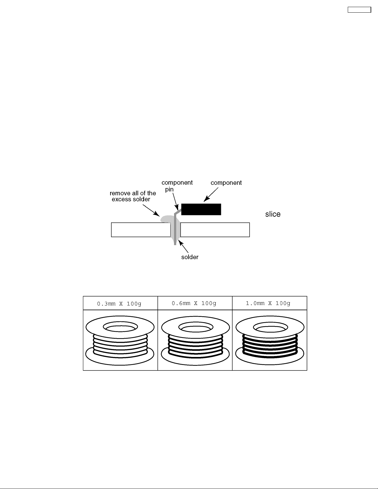
4 About lead free solder (PbF)
Note: Lead is listed as (Pb) in the periodic table of elements.
In the information below, Pb will refer to Lead solder, and PbF will refer to Lead Free Solder.
The Lead Free Solder used in our manufacturing process and discussed below is (Sn+Ag+Cu).
That is Tin (Sn), Silver (Ag) and Copper (Cu) although other types are available.
This model uses Pb Free solder in it’s manufacture due to environmental conservation issues. For service and repair work, we’d
suggest the use of Pb free solder as well, although Pb solder may be used.
PCBs manufactured using lead free solder will have the PbF within a leaf Symbol PbF stamped on the back of PCB.
Caution
·
· Pb free solder has a higher melting point than standard solder. Typically the melting point is 50 ~ 70 °F (30~40 °C) higher.
· ·
Please use a high temperature soldering iron and set it to 700 ± 20 °F (370 ± 10 °C).
·
· Pb free solder will tend to splash when heated too high (about 1100 °F or 600 °C).
· ·
If you must use Pb solder, please completely remove all of the Pb free solder on the pins or solder area before applying Pb
solder. If this is not practical, be sure to heat the Pb free solder until it melts, before applying Pb solder.
·
· After applying PbF solder to double layered boards, please check the component side for excess solder which may flow onto
· ·
the opposite side. (see figure below)
Suggested Pb free solder
There are several kinds of Pb free solder available for purchase. This product uses Sn+Ag+Cu (tin, silver, copper) solder.
However, Sn+Cu (tin, copper), Sn+Zn+Bi (tin, zinc, bismuth) solder can also be used.
7
Page 8
TC-32LX700
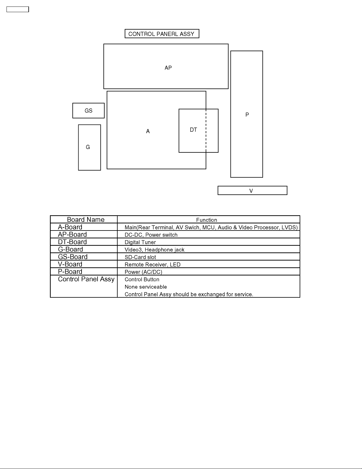
5 Chassis Board Layout
8
Page 9
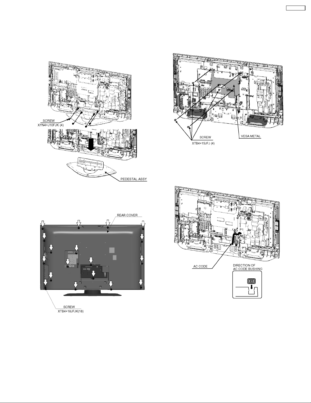
6 Disassembly for Service
TC-32LX700
6.1. Pedestal assy
1. Lay down the unit so that the rear cover faces upward.
2. Remove the 4 screws.
3. Remove the pedestal assy.
6.3. VESA metal
1. Remove the 4 screws.
2. Remove the VESA metal.
6.4. AC cord
1. Take out the groove of the AC cord from the slot of the
tuner cover.
2. Disconnect the connecter (P1) of AC cord.
6.2. Rear cover
1. Remove the 18 screws.
2. Remove the rear cover.
9
Page 10

TC-32LX700
6.5. Tuner cover
6.7. Control panel assy
1. Remove the 2 screws.
2. Remove the tuner cover.
6.6. Power button bracket
1. Remove the 2 screws.
2. Remove the power button bracket.
1. Disconnect the connecter (AP6).
2. Remove the 2 screws.
3. Remove the control panel assy.
6.8. G-Board and GS-Board
1. Remove the screw.
2. Disconnect the connecter (GS8)
3. Remove the GS-Board
4. Remove the 2 screws.
5. Disconnect the connecter (G4).
6. Remove the G-Board.
10
Page 11

6.9. Side AV bracket
TC-32LX700
6.11. P-Board
1. Remove the 2 screws (A).
2. Remove the screw (B).
3. Remove the side AV bracket.
6.10. AP-Board
1. Remove the 3 screws.
2. Disconnect the connecters (A3/A4/CN3).
3. Remove the AP-Board.
1. Remove the 6 screws.
2. Disconnect the connecters (P3/P5/P6).
3. Remove the P-Board.
6.12. DT-Board
1. Remove the 4 screws.
2. Remove the DT-Board.
11
Page 12
TC-32LX700
6.13. A-Board and DT-Board metal
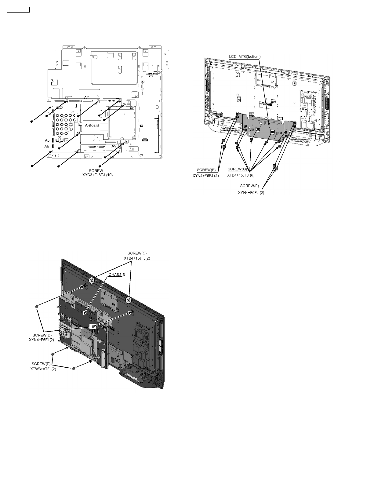
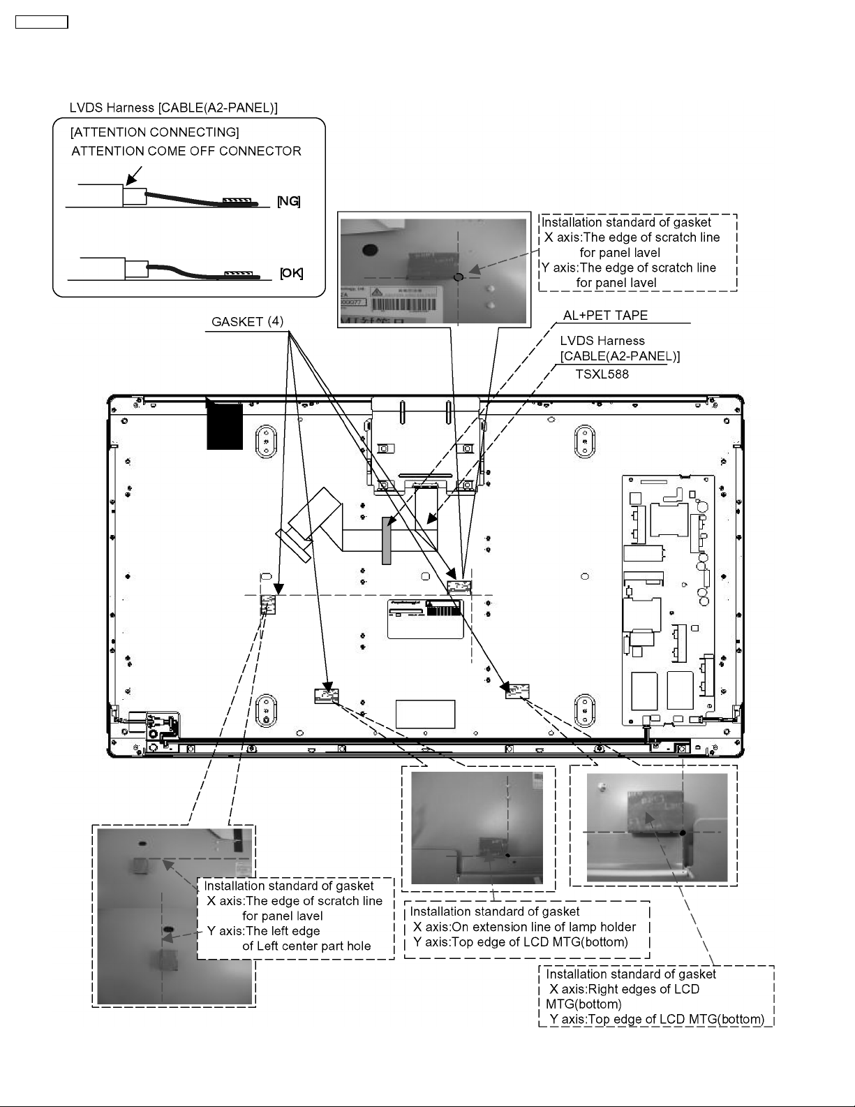
6.15. LCD MTG (bottom)
1. Remove the 10 screws.
2. Disconnect the connecter (A2/A5/A6/A9).
3. Remove the 2 screws.
4. Remove the A-Board and DT-Board metal.
6.14. Chassis
1. Remove the 4 screws (F).
2. Remove the 6 screws (G)
3. Remove the LCD MTG (bottom).
1. Remove the 2 screws (C).
2. Remove the 2 screws (D).
3. Remove the 2 screws (E).
4. Remove the chassis.
12
Page 13

6.16. Speaker assy
TC-32LX700
6.17. Squawker speaker
1. Remove the 4 screws.
2. Remove the speaker assy.
1. Remove the 4 screws.
2. Remove the squawker speaker.
6.18. V-Board
1. Remove the 2 screws.
2. Remove the V-Board.
13
Page 14
TC-32LX700
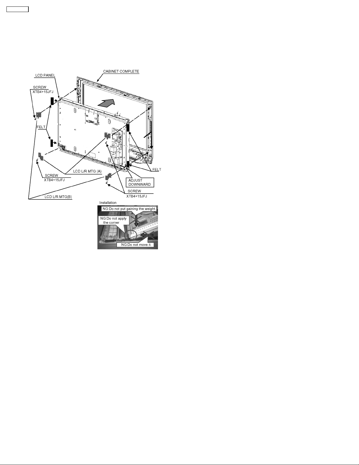
6.19. LCD panel
1. Remove the 2 screws.
2. Remove the LCD L/R MTG (A).
3. Remove the 2 screws.
4. Remove the LCD L/R MTG (B).
5. Remove the LCD panel.
14
Page 15

7 Caution statement
7.1. Caution statement.
Caution:
Please confirm that all flexible cables are assembled correctly.
Also make sure that they are locked in the connectors.
Verify by giving the flexible cables a very slight pull.
TC-32LX700
15
Page 16
TC-32LX700
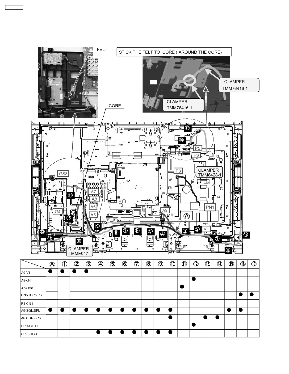
8 Location of Lead Wiring
8.1. Lead of Wiring (1)
16
Page 17

8.2. Lead of Wiring (2)
TC-32LX700
17
Page 18
TC-32LX700
9 EMI Processing
9.1. EMI (1)
18
Page 19

9.2. EMI (2)
TC-32LX700
19
Page 20

TC-32LX700
10 Self-check Function
Use the self-check function to test the unit.
1. Checking the IIC bus lines
2. Power LED Blinking timing
10.1. Check of the IIC bus lines
10.1.1. How to access
Self-check indication only:
Produce TV reception screen, and while pressing [VOLUME ( - )] button on the main unit, press [OK] button on the remote control
for more than 3 seconds.
Self-check indication and forced to factory shipment setting:
Produce TV reception screen, and while pressing [VOLUME ( - )] button on the main unit, press [MENU] button on the remote
control for more than 3 seconds.
10.1.2. Exit
Disconnect the AC cord from wall outlet.
10.1.3. Screen display
10.1.4. Check Point
Confirm the following parts if NG was displayed.
20
Page 21

10.2. Power LED Blinking timing chart
1. Subject
Information of LED Flashing timing chart.
2. Contents
When an abnormality has occurred the unit, the protection circuit operates and reset to the stand by mode. At this time, the
defective block can be identified by the number of blinkes of the Power LED on the front panel of the unit.
TC-32LX700
21
Page 22

TC-32LX700
10.3. No Power
First check point
There are following 2 states of No Power indication by power LED.
1. No lit
2. Red is lit then turns red blinking a few seconds later. (See 10.2.)
22
Page 23

TC-32LX700
11 Service Mode
11.1. How to enter into Service Mode
While pressing [VOLUME ( - )] button of the main unit, press [RECALL] button of the remote control three times within 3 seconds.
11.1.1. Key command
“1” button...Main items Selection in forward direction
“2” button...Main items Selection in reverse direction
“3” button...Sub items Selection in forward direction
“4” button...Sub items Selection in reverse direction
“VOL” button...Value of sub items change in forward direction ( + ), in reverse direction ( - )
11.1.2. Contents of adjustment mode
·
· Value is shown as a hexadecimal number.
· ·
·
· Preset value differs depending on models.
· ·
·
· After entering the adjustment mode, take note of the value in each item before starting adjustment.
· ·
Main item Sub item Sample Data Remark
ADJUST CONTRAST 000
COLOR 49
TINT FE
SUB-BRT 808
BACKLGT 276
B-Y-G 34
R-Y-A 00
WB-ADJ R-GAIN FF
G-GAIN FF
B-GAIN FF
R-CENT AD
G-CENT 80
B-CENT BA
OPTION BOOT ROM Factory Preset.
STBY-SET 00
Emergency ON
CLK MODE 00
CLOCK 000
RM-SET CODE A Fixed.
SRV-TOOL 00 See next.
11.1.3. How to exit
Switch off the power with the [POWER] button on the main unit or the [POWER] button on the remote control.
23
Page 24

TC-32LX700
11.2. SRV-TOOL
11.2.1. How to access
1. Select “SRV-TOOL” in Service man Mode.
2. Press [OK] button on the remote control.
11.2.2. Display of SOS History
SOS History (Number of LED blinking ) indicatrion.
From left side; Last SOS, before Last, three occurrence before, 2nd occurrence after shipment, 1st occurrence after shipment.
This indication will be cleared by “Self-check indication and forced to factory shipment setting”.
11.2.3. POWER ON TIME/COUNT
Time : Cumulative power on time, indicated hour : minute by decimal
Count : Number of On times by decimal
Note : This indication will not cleared by self-check or any command.
11.2.4. Exit
1. Disconnect the AC cord from wall outlet.
24
Page 25

12 Adjustment
12.1. Voltage chart of AP-board
VOLTAGE TEST POINT SPECIFICATION
24V TP7904 24.0±1.2V
SUB_5V TP7211 5.12±0.25V
SUB_9V TP7213 9.27±0.45V
BT_30V TP7601 31.5±2.5V
HQ_3.3V TP745 3.38±0.17
SOUND_15V TP7209 15.2V±0.75V
PANEL_12V TP7702 12.14±0.6V
STB_5V TP7151 5.0±0.5V
12.2. Voltage chart of P-board
VOLTAGE TEST POINT SPECIFICATION
STB_5V TP823 5.0±0.5V
12.3. Voltage chart of A-board
VOLTAGE TEST POINT SPECIFICATION
STB3.3V TP7006 3.3±0.16V
SUB1.2V TP5601 1.26±0.06V
SUB1.8V TP5602 1.83±0.09V
SUB3.3V TP5600 3.3±0.16V
MHQ1.2V TP4209 1.22±0.06V
MHQDDR2.5V TP4210 2.5±0.12V
TC-32LX700
12.4. Picture level adjyustment (RF)
Instrument Name Remarks
1. REMOTE TRANSMITTER
2. Ex. Signal (Sprit color bar)
Adjustment or Inspection Procedure Remarks
<procedure>
1. Receive the sprit color bar.
(Screen mode: ZOOM or FULL Picture mode: DYNAMIC AI: OFF AI Picture: OFF)
*BACK LIGHT +30
<Inspection>
1. Enter Service mode, and select MAIN_ADJ PICTURE.
Volume UP/DOWN key makes GAIN displayed under PICTURE to set.
Pushing the remote controller “OK” key for about 3 seconds, GAIN is suited
to the adjustment value automatically.
25
Page 26

TC-32LX700
13 Hotel mode
1. Purpose
Restrict a function for hotels.
2. Access command to the Hotel mode setup menu
In order to display the Hotel mode setup menu, please enter
the following command (within 2 second).
[TV] : Vol. “Down” + [REMOTE] : TV/VIDEO (3 times)
Then, the Hotel mode setup menu is displayed.
item Function
Mode Select hotel mode ON/OFF
Input Select input signal modes.
Channel Select channel when input signal is RF.
Volume Adjust the volume when each time power is
Vol. Max Adjust maximum volume.
OSD Ctrl Restrict the OSD.
FP Ctrl Select front key conditions.
Pow Ctrl Select POWER-ON/OFF condition when AC
Set the input, when each time power is
switched on.
Selection:
-/RF/COMP/HDMI1/HDMI2/VIDEO1/
VIDEO2/VIDEO3
·
· Off: give priority to a last memory.
· ·
Set the channel, each time power isswitched
on.
Selection:
Any channel number or “-”.
“-” means the channel when turns off.
switched on.
Range:
0to63
Range:
0to63
Selection:
OFF/PATTERN1
·
· OFF: No restriction
· ·
·
· PATTERN1: restriction
· ·
Selection:
Off/Pattern1/All
Off: altogether valid.
Pattern: only input key is valid.
All: altogether invalid.
power cord is disconnected and then
connected.
OFF: The same condition when AC power
cord is disconnected.
ON: Forced power ON condition.
3. To exit the Hotel mode setup menu
Disconnect AC power code from wall outlet.
4. Explain the Hotel mode setup menu
26
Page 27

14 Conductor Views
14.1. P-Board
6
TC-32LX700
P-BOARD (FOIL SIDE)
P
5
4
TZRXN010MRR
TP824
JS821
TP825
R831
R832
R830
R823
IC802
C821
TP823
R
C822
R822
1
6
P6
8
1
R833
P5
COLD
R829
ZA804
C827
19
D814
IC801
JS811
R826
D813
D819
D816
TP822
COLD
R821
D826
C818
R828
D802
ZA805
C808
TP812
LF804
TP811
P3
13
D824
C828
-
+
HOT
C826
Q802
R827
C823
R815
R814
Q801
C815
4
5
C811
TP821
D801
RL802
D823
ZA802
D822
RL801
C807
C806
HOT
1
P1
2
F801
T5AH AC250V
F802
TP803
ZA801
TP802
TP801
T5AH AC250V
TP804
CF801
C803
COLD
LF803
C802
D803
LF801
TNPA4154
SEE REVERSE FOR ORDER NO.
C801
R801
P
2
PbF
R802
ZA806
1
P2
ZA803
D825
R825
R824
K
A
D821
2
C817
PC801
S2
S1
T801
R811
C824
18
C825
D812
D817
C814
D811
C813
D818
V1
R813
V2
1
P1P2
C816
8
D815
R812
3
Parts Location
P-BOARD
(FOIL SIDE)
IC
IC801 C-4
IC802 A-4
TRANSISTOR
Q801 C-4
Q802 C-5
TP
TP801 G-4
TP802 G-4
TP803 G-4
TP804 G-4
TP811 D-4
TP812 D-4
TP821 E-5
TP822 C-5
TP823 A-4
TP824 A-5
TP825 A-4
P-BOARD (COMPONENT SIDE)
TZRXN010MRR
ZA803
1
COLD
J108
J106
D825
J104
ARK
IC802
1
1
C821
P6
T801
J102
S1S2
C827
P5
6
8
ZA804
3
2
HOT
TNPA4154
ORDER
NO.
D801
-
4
D824
1
+
LF804
34
1
2
J209
P3
13
C828
J306
C806
C807
COLD
T5AH AC250V
R
C803
ZA802
3
4
12
RL801
1
2
1
CF801
RL802
J301
2
L
ZA801
CAUTION
2
J205
R802
ZA806
1
F801
F802
FOR CONTINUED PROTECTION AGAINST RISK OF FIRE,
REPLACE ONLY WITH ’LITTELFUSE’ TYPE ’215’.
R801
C801
T5AH AC250V
R
D803
L
LF801
COLD
P1
21
J307
C802
R
413
2
L
34
12
LF803
PbF
P
2
R828
J109
J304
D826
4
1
C818
J305
HOT
J201
R812
ZA805
COLD
R821
3
2
D802
C808
JS812
C811
IC801
J208
19
P2
18
C813
D819
D818
1
4
C816
8
5
2
J204
PC801
V1 V2 P1 P2
Parts Location
P-BOARD
(COMPONENT SIDE)
IC
IC801 F-1
IC802 G-2
TC-32LX700
P-BOARD TZRXN010MRR
ABCDEFGH I
TC-32LX700
P-BOARD TZRXN010MRR
27
Page 28

TC-32LX700
14.2. AP-Board
AP
Parts Location
AP-BOARD (FOIL SIDE)
IC
6
IC7205 E-2
IC7209 H-2
IC7212 B-3
IC7215 F-2
IC7216 H-4
IC7217 H-3
IC7233 D-2
TP
TP7151 C-3
TP7207 C-2
TP7208 F-2
TP7209 E-2
AP-BOARD (FOIL SIDE)
5
TNPA4155ABS
R7301
Q7224
R7314
R7312
Q7223
R7313
SW7203
JS7974
JS7975
JS7979
JA11
JS7977
JS7973
JS7976
R7331
C7344
R7332
1
AP6
2
C7258
TP7210 E-2
TP7211 D-2
TP7212 H-3
TP7213 G-2
TP7451 C-2
TP7601 G-3
TP7701 B-2
TP7702 C-2
TP7801 H-3
TP7802 I-3
TP7803 H-3
TP7904 A-2
TP7905 B-3
4
TRANSISTOR
Q7204 C-3
Q7205 C-4
Q7206 C-3
Q7207 D-4
Q7208 B-1
Q7209 B-1
Q7210 C-1
Q7211 D-1
Q7212 B-1
Q7213 B-1
Q7214 B-1
Q7221 A-2
Q7222 A-2
Q7223 B-4
Q7224 A-4
Q7225 F-2
Q7226 E-2
Q7227 H-2
Q7228 F-2
Q7229 E-2
Q7230 H-2
Q7450 D-2
Q7451 C-1
Q7452 B-2
Q7508 B-2
Q7701 B-2
Q7702 B-2
Q7804 H-4
Q7805 F-2
Q7806 F-1
L7802
C7808
5
C7804
ZA7002
C7809
C7807
R7802
C7806
C7805
TP7802
C7803
R7803
R7801
R7215
R7214
R7212
Q7207
R7216
R7217
C7207
D7261
D7203
D7204
C7204
R7210
Q7204
R7208
R7209
Q7205
R7213
C7206
C7205
R7211
Q7206
L7801
L7701
TP7701
L7702
R7364
D7220
R7501
R7241
D7476
R7496
D7805
R7502
R7493
D7472
R7705
D7473
R7250
D7470
R7499
Q7451
R7492
JA19
D7475
D7469
R7353
L7703
D7481
R7247
D7208
R7497
L7704
C7708
R7362
C7703
D7474
R7309
R7706
TP7702
D7704
R7488
C7705
R7487
TP7151
L7315
L7452
D7703
R7486
TP7451
D7480
R7485
C7248
C7246
R7243
C7251
D7471
R7234
D7240
L7207
C7245
TP7207
D7237
Q7210
JA5
AP8
3
R7268
R7267
C7302
2
AP2
ZA7006
1
15
JA4
R7266
Q7221
R7336
JA2
Q7222
R7357
R7355
R7356
R7354
1
1
15 14
C7101
2
2
1819
R7265
C7214
INV_SOS
ADIM
INV_PWM
C7100
L7316
TP7904
R7225
D7206
R7219
D7222
R7221
R7701
C7208
C7707
R7704
C7706
R7344
Q7701
Q7208
R7703
R7222
R7220
C7704
R7270
R7702
C7215
R7712
R7269
5
5
4
4
R7710
R7226
R7245
TP7905
Q7508
Q7209
R7707
IC7212
3
3
2
2
1
1
R7345
R7711
R7239
R7232
Q7213
D7702
Q7702
R7708
R7709
Q7212
R7238
R7233
R7237
R7242
Q7214
R7498
D7701
C7701
C7702
D7705
R7311
R7495
Q7452
C7212
C7244
R7228
D7236
R7218
C7210
L7450
2
3
D7224
R7299
1
L7201
C7252
C7209
JA8
D7205
Q7450
R7453
5
R7302
IC7233
4
D7260
Q7211
R7343
R7342
C7249
D7223
L7214
L7215
TP7211
D7453
D7452
R7304
R7305
C7247
C7278
R7366
C7279
D7251
C7211
C7298
D7250
R7287
R7223
R7229
L7213
R7224
C7274
D7207
C7275
D7252
D7249
R7227
JA3
D7247
L7212
C7273
C7272
D7248
TP7210
R7325
C7284
Q7226
IC7205
R7328
1
C7601
D7602
C7605
D7258
C7603
D7259
L7217
L7312
C7299
C7288
D7256
D7468
C7300
R7363
L7302
1
TP7213
L7960
2
C7287
D7253
C7956
R7310
TP7212
C7286
C7285
10
D7254
D7255
C7294
R7337
C7293
L7216
1
IC7209
C7958
R7494
D7804
JA10
AP
TNPA4155
1
SEE REVERSE FOR ORDER NO.
PbF
R7307
R7349
JA13
C7270
C7263
R7346
R7327
R7351
R7317
R7303
L7219
L7218
R7805
C7612
C7611
C7602
C7292
C7291
C7606
L7953
L7600
D7601
L7965
22
23
TP7601
C7610
C7609
C7965
C7954
R7322
R7320
R7329
10
C7282
Q7229
C7277
R7324
C7283
R7323
C7281
C7280
R7326
R7347
L7210
L7211
R7321
JA17
C7276
JA18
C7266
R7348
D7245
JA1
L7208
C7265
C7261
D7244
C7262
TP7209
D7246
JA16
L7209
D7243
D7242
C7259
R7316
D7241
C7271
IC7215
TP7208
1
R7804
R7350
JA6
JA7
2
C7269
1
JA14
JA15
R7319
R7318
Q7225
10
Q7805
Q7806
JA9
AP4
R7306
C7267
R7300
R7315
C7268
Q7228
C7952
C7264
C7260
R7341
D7803
R7335
AP3
R7340
D7802
L7966
C7967
C7801
R7490
C7961
Q7804
C7295
TP7803
C7301
R7308
TP7801
C7802
C7303
Q7227
Q7230
IC7216
C7957
R7339
R7358
L7956
1
C7966
IC7217
R7334
22
23
R7333
C7289
C7297
R7330
R7338
C7290
L7959
C7304
R7352
R7360
C7296
JA12
C7963
1
D7801
R7365
R7361
5
L7964
TC-32LX700
AP-BOARD TNPA4155ABS
ABCDEFGH I
TC-32LX700
AP-BOARD TNPA4155ABS
28
Page 29

TC-32LX700
AP
Parts Location
6
AP-BOARD
(COMPONENT SIDE)
IC
IC7205 E-2
IC7209 B-2
IC7212 H-2
IC7215 D-2
IC7233 F-2
5
2
1
AP6
SW7203
J18
J135
PbF
J123
3
3
J1
1
1
4
4
IC7212
D7705
J145
J118
J105
TNPA4155
ORDER
NO.
1
J102
JS7200
JS7201
AP8
5
J111
J149
J116
L7316
JS7153
J126
J14
J142
JS7226
JS7309
24V
AP2
1
2
1
2
14
15
18
19
ZA7006
J311
52
52
J10
J334
J314
AP
1
AP-BOARD (COMPONENT SIDE)
4
3
2
1
TNPA4155ABS
J19
C7803
L7959
L7964
J330
J148
L7956
JS7957
C7802
JS7852
22
23
ODU_15V
J20
J108
DTV_9V
C7966
L7802
J21
ZA7002
J340
J333
C7967
J104
L7801
JS7801
L7966
C7286
10
IC7209
1
L7216
AP3
SUB_9V
J318
JS7225
D7254
J307
J325
C7300
SOUND_VCC
C7299
J329
JS7227
L7217
L7302
JS7204
2
1
JS7962
BT_30V
L7960
J133
C7288
L7312
J301
J120
STB_5V
L7953
L7218
L7219
J130
J122
J313
L7600
J315
HQ_3.3V
J2
JS7963
L7965
23
J158
J7
C7606
SUB_5V
J331
JS7966
22
J312
J140
J305
J309
J134
J121
J117
J310
J110
INV_ON
AP4
J317
J304
2
C7260
J157
IC7215
110
1
L7208
JS7219
D7242
J101
C7262
L7209
J139
L7210
J322
J335
J316
J337
J156
J336
J119
L7211
J319
J303
J146
J151
J332
J137
C7273
10
IC7205
1
J144
J109
J308
JS7222
D7248
L7212
C7275
J323
J302
J113
J143
C7298
L7214
J103
J8
J129
L7213
C7211
J306
IC7233
J3
J136
J132
L7215
J147
J124
JS7456
JS7228
J106
J338
L7452
L7315
L7450
JS7450
C7245
C7246
134
J17
J328
L7201
2
D7240
C7209
L7207
5
PANEL_12V
J13
J5
J141
C7708
C7703
J128
J339
J114
J127
J112
L7704
JS7702
J150
L7703
J138
J321
J15
L7702
C7344
L7701
JS7701
C7702
J9
TC-32LX700
AP-BOARD TNPA4155ABS
ABCDEFGH I
TC-32LX700
AP-BOARD TNPA4155ABS
29
Page 30

TC-32LX700
14.3. A-Board
A-BOARD (FOIL SIDE)
TNPH0683S
R4303
C4346
TP4243
C4253
C4218
C4222
C4223
C4256
C4245
TP4513
JS4500
L4513
L4512
C4561
FL4501
L4521
R4301
TP4232
C4252
C4259
C4279
L4510
JS4504
R4687
L4503
TP4243
R4328
R4330
R4332
C4254
C4257
C4255
C4234
+
R4299
R4297
R4300
TP4210
TP4512
L4519
R4688
R4541
L4507
TP4503
D4520
TP4230
TP4231
C4404
C4405
C4260
C4261
C4242
C4329
C4301
C4325
C4302
C4304
C4315
TP4210
C4577
+
TP4501
D4517
C4224
C4215
C4216
C4221
C4535
C4534
TP4512
TP4514
R4543
TP4229
C4317
A31
C4406
C4285
C4262
C4247
R4708
Q4503
TNPH0683 B
TP4223
TP4227
TP4228
TP4225
TP4224
TP4226
TP4244
TP4244
TP4223
TP4230
TP4245
TP4232
TP4227
TP4233
7
C4233
C4533
C4608
L4506
1
C4209
C4408
C4217
C4220
C4274
C4232
C4327
C4326
R4589
R4595
R4588
R4594
R4695
R4592
R4533
R4530
TP4225
TP4228
TP4231
TP4233
TP4229
C4386
C4393
C4390
FL4206
C4388
C4392
R4349
R4350
R4348
R4347
C4375
C4382
C5771
TP5727
TP4240
TP5727
A31
TP4241
Q5709
TP4242
C4415
C4412
C4407
C4282
C4225
C4207
C4208
C4284
C4286
C4219
C4240
C4258
C4401
C4213
C4283
C4214
C4267
C4271
C4268
C4270
C4281
C4280
C4227
C4400
C4239
C4273
C4272
C4263
C4248
C4275
C4276
C4250
C4230
C4231
C4236
R4256
C4237
C4265
C4266
C4264
C4278
R4290
C4319
R4400
C4328
C4321
R4289
C4303
C4324
C4312
C4323
R4298
C4330
C4298
C4314
C4316
R4296
C4300
C4299
C4305
+
C4296
C4530
R4582
R4579
R4584
R4575
C4524
R4577
C4529
R4578
R4581
R4574
R4583
R4576
C4523
R4587
R4593
TP4505
D4527
C4532
R4586
D4526
TP4505
C4509
C4606
Q4503
Q4504
Q4504
R4544
D4515
R4546
R4525
R4507
C4505
R4547
R4545
Q4505
TP4506
Q4505
TP4506
R4663
R4372
TP5726
TP4224TP4226
FL4207
L4211
C5772
C5773
R5754
Q5709
C4269
C4226
C4238
C4249
TP4508
C4703
TP4216
TP4221
TP4222
R4371
TP4221
TP4218
TP4219
TP4222
TP4220
C4389
C4387
+
Q5708
R5755
C4200
JS4202
JS4200
JS4201
C4202
R4241
R4242
C4201
R4239
C4402
C4210
TP4246
C4251
R4255
C4725
C4599
C4629
TP4508
R4662
C5769
TP5726
C4714
TP4220
TP4216
TP4217
C4724
R4240
R4224
R4225
R4226
R4710
TP4214
TP4215
C4377
C4380
C4376
Q5708
R4238
R4220
R4221
R4222
R4223
C4344
C4347
C4349
C4350
C4348
C4352
C4351
TP4246
TP4206
5
8
R4713
TP5728
TP4218
TP4219
C4398
C4345
JS4209
JS4210
TP4213
TP4206
R4712
TP5728
TP4236
L4214
JS4208
JS4207
L4216
L4217
C4367
TP4213
TP4207
C4540
C4628
C5775
TP4217
C4331
TP4208
R5757
R5756
TP4211
L4215
TP4207
D4203
C4742
R4711
IC4515
TP4208
TP4211
C4342
C4343
C4341
TP4212
C4399
R4254
IC4515
C4340
TP4214
TP4215
C4715
C4370
4
5
C4397
4
5
C4360
4
C4369
TP4212
JS4203
JS4206
JS4212
5
4
1
TP4101
C4287
TP4101
L4202
C4295
C4306
C4307
C4780
IC4204
JS4204
L4218
C4353
3
C4332
IC4204
C4338
C4336
1
JS4205
L4206
C4335
C4333
IC4205
C4339
C4337
13
JS4211
L4219
L4207
C4362
C4354
C4361
3
IC4206
C4364
C4363
1
IC4206
C4723
C2107
C2105
IC2106
R2287
TP4507
TP4507
L4205
C2101
C2109
C2115
C2110
C2120
C2124
C2121
C2050
R2111
R2056
R2057
R2010
R2009
D4200
TP4209
+
C2106
C2100
TP4105
TP4209
R4288
L4200
IC4205
80
20
TP4102
C4206
C4334
1
C4076
C4078
L4091
TP4102
8
C4289
IC4202
C4288
1
C4297
DVISOUND1
COMPONENT1
C2108
C2268
R2151
R2100
21
R2008
C2023
TP4103
TP4104
TP4106
TP4106
TP4108
D1111
TP4105
TP4104
IC4202
D4201
TP4107
R1343
R1400
C4754
C4293
R4284
R1405
R4902
R1406
5
R1528
D1120
D1112
D1113
TP4107
R1104
R4287
4
R4286
R1139
R1140
C4700
R1249
R2619
TP7006
TP4109
TP4110
C4721
C4716
R3212
R3211
R3209
TP4103
D4202
C4203
V1
V2
MONOUT
C2113
C2114
C2267
C2263
C2264
R2150
C2191
C2196
C2190
C2186
C2102
61
IC2106
R2276
C2048
C2052
C2053
R2013
C2054
L2021
40
R2164
IC1108
TP4108
TP7006
R2624
R1235
R1260
TP4111
C2133
60
C2126
TP1104
D3065
D3066
TP7005
IC1108
C1193
TP4109
R1129
TP1104
C4734
C4713
C2246
C2057
C2049
41
TP2101
TP2037
TP4113
TP7005
TP4114
FL4048
TP4114
R1356
TP4112
C1196
C1197
TP4112
C1195
C1105
R1152
C1194
R1146
96
R1229
TP4111
TP4110
R1134
R1144
97
R1123
C1104
IC1100
R1124
R1125
128
R1130
R1237
R1253
132
R1222
R1259
C4762
R1251
R1216
R1217
D1104
D1110
C1119
JS3122
FL3032
D3064
C3177
D3052
R3199
D3049
R3205
D3050
R3197
C4741
L2040
R2149
1
4
C2134
IC2011
IC2011
C2173
R2165
C2171
5
8
R2203
C2270
R2204
C2271
R2319
D2016
L2034
R2099
R2205
R2206
R2325
L2035
R2098
D2017
R2270
R2271
TP2101
C4774
R2320
R2326
JS2075
C2302
Q2301
R2302
Q2301
R2301
TP2037
D2301
R2331
R2330
C2301
R2305
JS2078
TP1105
TP4113
TP3006
TP1102
TP3006
TP1102
TP1100
TP1100
C1126
R1169
R1166
R1223
R1170
R3081
C3081
D3048
JS3115
JK3000
TP1101
D1105
R1183
R1184
R1243
R1232
TP1101
R1186
R1247
R1248
R1218
R1240
R1241
R1220
R1191
TP3016
R1192
TP1103
R1174
TP3009
R1175
D1109
TP3019
R1177
R1272
R1178
R1179
C1116
R1194
R1181
R1196
C1111
D1115
C4753
C3047
C3045
R3032
IC3001
R3085
R3083
C3091
C3089
R3084
R3087
C3087
C3090
C3088
JS3112
FL3034
C3104
C3107
C3106
C3108
C3103
C3105
R3104
R3103
R3107
R3108
R3106
1
IC3101
33
R3124
R3125
R3126
C3133
C3132
R3147
Q3124
C3124
R3150
C3123
R3149
R3145
R3146
Q3123
C4712
Q3123
C1123
C1109
R1149
C1125
R1164
65
64
R1244
R1246
R1158
IC3001
JS3116
C3112
C3113
C3116
C3117
C3120
C3121
C1114
33
R1245
R1273
C1112
R1162
R1165
R1234
R1203
R1171
R1172
D1106
C1124
C3049
C3048
50
51
C3051
C3053
C3055
C3057
C3059
C3061
C3063
R3064
C3065
C3067
C3069
C3072
C3074
75
C3076
76
R3079
R3077
C3086
C3079
C3077
FL3030
Q2693
Q2693
C3109
C3111
C3110
R3111
R3110
R3109
R2622
11
12
R3112
R3113
C3164
IC3101
C3165
R3116
R3117
C3118
C3119
R3120
22
R3121
R3122
23
C3146
R3123
C3145
L3101
C4732
IC1100
R1250
R1266
R1231
R1155
R1168
R1167
TP1105
C1113
JS3121
D3051
R3203
Q2694
Q2694
R2623
C3176
D3005
D3005
D3152
C2323
C2321
C2319
C2317
R2362
R2322
D2303
C2324
C2322
C2320
D2304
C2318
R2324
L2308
L2309
TP3004
JS2076
C3397
TP3003
TP3004
C3096
C3399
L3034
L3033
C3098
TP3008
TP2710
R2837
TP3001
TP3001
D5702
R5772
R5771
C5778
R5768
Q5714
R5769
Q5714
R2835
D2835
R2836
TP2708
TP2709
D2836
D2837
TP1103
TP3016
TP3009
TP3019
IC5700
R5730
C5750
C5749
C5748
IC5700
R5732
R5731
C5753
L5705
L5706
R3033
C3032
26
C3024
C3025
25
C3022
R3020
C3020
R3019
R3026
C3018
C3017
C3014
R3014
C3012
C3010
C3008
C3006
R3005
C3005
1
C3003
R3003
R3002
100
C3001
R3001
R3095
R3099
C3093
R3096
R3097
C3097
C3095
C3099
JS3118
D3047
FL3031
C4711
JS3111
JS3114
C3102
C3101
FL3029
C3144
44
C3143
C3142
C3141
C3140
C3139
C3138
R3137
R3136
R3135
C4773
R8566
R3134
34
R8565
Q3124
R3148
D2057
R3153
C3153
R3151
Q3125
6
2
3
R3152
R8562
R3154
R8563
R8564
Q3125
C2351
6
Q2064
Q2064
JS2072
C2349
L2310
IC2303
D2302
IC2303
C2350
C2352
TP3002
Q5713
3
R2107
R2122
Q2060
R4016
L3037
TP3007
Q5713
R2834
D2834
TP2707
L5707
C5760
C5752
D3073
D3072
D3068
D3067
D3063
JS3117
D3080
D3079
D3060
JS3053
FL3037
JS3113
R3207
D3062
D3061
7
1
FL8500
10
1
FL8501
2
Q2063
R2106
R2108
Q2065
R2109
C2104
R2120
JS2074
Q2059
R2141
R2142
TP3017
TP3005
4
5
7
C2125
R2154
3
IC5702
R2145
R2153
Q2053
R2148
JS2040
D2061
Q2053
C4701
D2059
JS2042
TP3005
TP3015
TP3015
D2831
C5762
IC5702
R5740
C5758
C4752
C5756
1
Q2059
C2103
A
JK3000
TP3055
TP3054
TP3053
TP3052
Q2063
JS2071
JS2073
TP3051
TP3050
A6
TP2310
TP2307
A6
TP2305
TP2303
15
A5
TP2309
4
TP2308
TP2306
A5
TP2304
1
Q2060
TP3007
TP3017
R5773
R2832
D2832
TP2711
D5701
R3193
R3192
R2838
R3191
R3190
C4733
R3208
R3204
R3202
R3201
R3196
D3076
D3078
D3077
10
Q2065
C4704
Q4202
Q4202
C4368
Q4203
C4308
L4213
Q4203
IC4208
C4378
C4411
4
C4309
D4207
R4392
IC4208
C4410
13
5
C4381
TP4235
C4409
L4220
C4358
C4359
8
R4327
1
4
C4413
TP8547
C4318
R4391
R4329
IC4209
R4331
5
R4334
R4295
C4414
R4227
R4228
R4229
C4403
R4333
R4335
C4246
C4235
C4277
C4244
C4243
R4399
R4291
R4293
R4292
5
C4320
C4322
C4311
1
FL4200
L4204
C4313
C4310
TP4513
C4588
C4586
R4624
C4558
C4538
+
C4543
C4544
C4565
C4539
R4611
C4564
C4584
C4579
C4585
C4508
C4576
R4612
C4563
C4562
FL4505
FL4504
L4520
C4580
R4540
TP4514
D4528
R4552
TP4517
TP4516
8
1
C4769
C5631
C5630
D5603
C5626
R5625
R5626
R5619
R5637
R5622
30
C5622
C5617
IC5601
C5620
R5632
R5630
C5624
1
R5614
C5621
C5616
R5617
R5623
R5633
R5616
R5621
R5634
TP5602
D5607
TP5602
R5611
C5606
R5612
C5600
D5600
R5600
12
C5601
IC5600
TP5600
R5610
TP5600
C4795
R4674
TP4509
IC4504
IC5600
13
C5643
R5606
R5602
C5608
R5607
R5603
R5618
C5605
R5613
D5606
C4720
C4781
Q4509
Q4509
R4568
R4569
TP4510
TP4511
TP4510
TP4511
5
4
C4717
TP8546
TP8545
JS2805
TP3061
TP3060
FL2805
TP3060
JS2807
FL2807
D5604
R5627
16
C5604
R5601
TP8548
TP3061
C5610
C5625
R5624
R8862
R8861
R8860
C5632
L5605
C5627
R5628
R5620 R5636
R5615
C5623
IC5601
15
C5603
1
R5604
C5607
24
R5605
R8850
R8903
R8904
R8864
R8899
TP8544
TP4234
C4719
Q5603
R5642
C5644
R5629
TP5601
TP4234
TP8501
TP8500
C8042
Q5603
R5647
R5638
R5646
R5640
R5641
R5635
R5631
TP5601
C5641
D5608
L8861
L8863
C8863
C8035
Q5604
C8050
Q5604
R8034
C8045
R8038
R5643
R8015
R8080
R8020
R8029
R8016
R8028
R8019
C8080
L8003
R8875
R8547
R8544
R8546
C5638
R8545
R8769
R8865
C5633
TP8552
C8861
TP8552
TP8553
C4763
TP8553
R8101
+
C8044
C8041
C8049
C8046
C8064
C8065
R8104
R8060
R8103
R8031
C8039
R8032
R8056
R8067
R8035
R8012
R8011
R8079
R8030
R8099
R8098
R8008
R8007
R8083
C8043
R8082
R8084
C8077
C8038
C8006
R8573
R8725
C8026
R8500
R8504
R8517
R8770
R8580
C5640
R8772
R8663
IC8503
5
R8558
R8554
R8555
R8557
4
IC8503
1
TP8551
8
C8506
R8556
R8075
C8010
R8578
R8100
R8078
C8016
C8023
C8024
R8519
R4384
TP5850
R8037
C8036
C8040
R8097
R8061
R8081
R8069
R8068
R8071
R8059
C8011
C8051
C8015
C8017
C8009
C8007
C8021
C8019
C8022
L8002
C8028
R8001
R8002
C8001
R8532
TP5850
R8033
C8012
C8013
R8086
C8048
R8048
R8025
R8053
R8049
R8052
R8039
R8024
R8077
C8037
C8078
L8004
L8010
C8074
C8076
C8075
C8073
C8008
L8006
C8020
C8032
C8018
C8072
C8002
R8584
R8604
R8542
R8540
R8539
R8538
R8552
R8553
R8550
R8548
C8052
C8047
R8023
R8045
R8041
C8014
R8040
R8044
C8079
R8110
R8111
R5762
C8071
C8070
R4341
L8008
L8009
C8034
R8764
R8765
C8033
C8025
C8027
R4343
R4342
C8029
R8518
R8724
IC8004
R8106
R8767
R8796
R8088
R8087
R8090
R8089
C8056
8
C8053
1
C8054
R8091
IC8004
C8055
X8001
16
9
R8093
C8062
C8061
R8109
C8057
R8094
C8058
C8060
L8005
C8059
C8067
R8107
C8068
C5637
R8586
R8587
L8001
C8030
C8031
R4215
R4216
R4209
R8866
R8867
R4336
R8005
C8003
R8003
R8004
C8005
C8004
R4337
R4213
R4214
TP4235
R8095
C4771
C5634
IC4209
ORDER NO.
L8007
C5639
R4413
TP4400
TP4400
TP8547
L4201
R4088
C4241
TP8551
IC4203
29
C8502
C8501
C8500
IC8502
56
TNPH0683
REVERSE FOR SUFFIX.SEE
C4782
C4777
C4776
C4718
28
C8504
R8510
R8512
IC8502
1
L4518
R8514
1
PbF
A
TP4515
C4745
R4696
C4570
C4573
FL4502
IC4509
L4515
C4620
C4618
R4709
R4682
R4680
R4681
1
R4676
5
8
C4621
C4623
IC4514
C4627
1
4
8
C4609
R4678
R4679
Q4502
Q4502
D4518
FL4506
R4654
C4615
4
IC4509
5
R4752
R4753
C4607
IC4203
C4743
C4616
C4617
R4528
R4532
TP4502
TP4500
D4512
C4744
C4614
IC4514
L4502
C4619
TP4515
C4596
C4605
IC4507
R4707
C4592
3
1
C4591
C4556
C4557
IC4507
C4603
4
C4611
C4610
C4612
C4613
D4513
L4505
L4504
C4560
5
FL4503
C4559
L4517
C4555
C4550
C4547
R4631
C4594
C4597
C4601
C4593
C4595
C4598
D4524
D4525
TP4504
R4539
R4538
TP4504
R4542
Q4500
Q4500
R4506
C4504
R4524
Gasket
6
5
4
TP4517
3
IC4504
2
1
TC-32LX700
A-BOARD TNPH0683S
ABCDEFGH I
TC-32LX700
A-BOARD TNPH0683S
30
Page 31

TC-32LX700
A
Parts Location
IC
IC1100 F-5
IC1108 E-6
IC2011 F-2
IC2106 E-2
IC2303 G-1
IC3001 F-5
IC3101 F-3
IC4202 E-6
IC4203 C-3
IC4204 E-5
IC4205 E-4
IC4206 E-4
IC4208 C-6
IC4209 C-5
IC4504 A-3
IC4507 C-3
IC4509 B-2
IC4514 C-2
IC4515 D-2
IC5600 A-5
IC5601 A-5
IC5700 F-5
IC5702 G-5
IC8004 C-6
IC8502 B-3
IC8503 B-4
A-BOARD (FOIL SIDE)
TRANSISTOR
Q2053 G-6
Q2059 G-6
Q2060 G-6
Q2063 G-3
Q2064 G-3
Q2065 G-2
Q2301 F-1
Q2693 F-4
Q2694 F-3
Q3123 F-3
Q3124 F-3
Q3125 F-3
Q4202 D-6
Q4203 C-6
Q4500 C-1
Q4502 C-2
Q4503 D-2
Q4504 D-2
Q4505 D-1
Q4509 A-3
Q5603 A-6
Q5604 B-5
Q5708 D-5
Q5709 D-5
Q5713 G-6
Q5714 G-6
TP
TP1100 F-6
TP1101 F-6
TP1102 F-6
TP1103 F-5
TP1105 F-5
TP2037 E-1
TP2101 E-2
TP3001 G-6
TP3004 G-6
TP3005 G-6
TP3006 F-6
TP3009 F-5
TP3015 G-5
TP3016 F-5
TP3017 G-6
TP3019 F-5
TP3060 A-1
TP3061 A-1
TP4101 E-6
TP4102 E-6
TP4103 E-6
TP4104 E-6
TP4105 E-6
TP4107 E-5
TP4109 E-5
TP4110 E-5
TP4111 E-5
TP4112 F-6
TP4113 F-6
TP4114 F-6
TP4206 D-4
TP4207 D-4
TP4208 D-5
TP4209 E-5
TP4210 D-3
TP4211 D-5
TP4212 E-4
TP4213 D-4
TP4214 E-6
TP4215 E-6
TP4216 D-6
TP4217 D-6
TP4218 D-6
TP4219 D-6
TP4220 D-6
TP4221 D-6
TP4222 D-6
TP4223 D-6
TP4224 D-6
TP4225 D-6
TP4226 D-6
TP4227 D-6
TP4228 D-6
TP4229 D-6
TP4230 D-6
TP4231 D-6
TP4232 D-6
TP4233 D-6
TP4234 A-1
TP4235 C-5
TP4243 D-6
TP4244 D-6
TP4246 D-4
TP4400 C-4
TP4504 C-2
TP4505 D-2
TP4506 D-1
TP4507 E-1
TP4508 D-2
TP4510 A-3
TP4511 A-3
TP4512 D-2
TP4513 D-3
TP4514 D-2
TP4515 C-2
TP4517 A-3
TP5600 A-4
TP5601 A-5
TP5602 A-5
TP5650 B-4
TP5726 D-1
TP5727 D-5
TP5728 D-2
TP7005 E-6
TP7006 E-5
TP8547 C-4
TP8551 B-4
TP8552 B-4
TP8553 B-4
Parts Location
IC
IC1101 B-6
IC2008 C-2
IC2013 C-3
IC2107 D-1
IC2301 B-2
IC2302 B-1
IC3017 E-5
IC4200 E-5
IC4201 E-3
IC4207 D-5
IC4500 E-2
IC4501 E-2
IC4506 D-2
IC4508 D-2
IC4510 E-2
IC4513 E-2
IC5701 A-5
IC8001 F-5
IC8002 F-5
IC8003 F-5
A-BOARD (COMPONENT SIDE)
TRANSISTOR
Q1107 B-5
Q1108 B-5
Q1109 B-5
Q1110 B-5
Q2018 C-2
Q2033 C-5
Q2035 C-5
Q2036 C-5
Q2040 C-5
Q2041 C-2
Q2042 C-2
Q2056 A-6
Q2057 A-6
Q2066 C-3
Q2302 B-2
Q2303 C-2
Q4200 C-6
Q4201 D-6
Q4204 E-5
Q4205 E-5
Q4206 E-5
Q4207 E-5
Q4501 D-2
Q4511 D-3
Q4512 D-3
Q4513 D-2
Q4514 D-3
Q4515 D-3
Q4516 D-2
Q4517 E-2
Q5600 G-4
Q5601 G-5
Q5602 G-5
Q5703 A-5
Q5706 D-2
Q5707 D-2
Q5710 D-2
Q5711 D-1
Q5712 B-5
TP
TP1110 C-5
TP8002 E-4
TP8003 E-5
TC-32LX700
A-BOARD PARTS LOCATION
TC-32LX700
A-BOARD PARTS LOCATION
31
Page 32

TC-32LX700
A-BOARD (COMPONENT SIDE)
TNPH0683S
R4363
IC4506
Q5706
Q5710
51
R4364
R4368
R4367
R4366
R4365
51
IC4207
75
R4243
C4211
X4200
R4253
X4201
R4252
R4261
C4541
R4606
R4604
4
IC4506
5
C4531
R4585
R5760
R5761
Q5710
R5759
C5776
R5758
Q5711
C4073
TNPH0683 A
A2
11
11
1
R4370
R4369
FL4202
FL4203
FL4204
FL4201
IC4207
76
C4379
R4245
R4244
1
A
R4247
R4246
R4273
R4272
R4267
R4268
R4264
R4262
R4263
R4277
L4509
C4536
C4525
Q4512
Q4511
C4546
C4604
C4545
C4600
C4602
R4706
1
Q4513
IC4508
IC4508
7
5481
C4583
C4587
C4528
C4527
R5753
R5752
Q5706
Q5711
ZA4005
Q4516
R4622
C4581
C4775
1
C4796
L4516
Q5707
R5751
4
Q4501
Q5707
C5770
R5750
C4072
ZA4002
A13
R4304
A2
1
FL4205
R4414
R4401
R4373
C4395
C4394
C4384
C4391
R4361
R4356
R4354
R4352
1
100
R4250R4673
R4248
R4234
R4251
R4230
R4249
IC4200
R4275
R4276
R4269
R4271
IC4201
C4551
L4511
D4530
C4526
Q4515
Q4515
Q4512
Q4514
Q4511
Q4514
R4667
R4602
R4580
R4693
Q4517
Q4513
C4625
R4598
Q4516
1
R4668
4
R4531
C4511
IC4501
R4505
R4527
R4503
Q4501
C4503
D4501
C4501
R4501
C4765
C4731
L4212
2650
25
C4383
C4396
R4360
R4385
R4357
R4355
R4353
R4351
C4385
L4210
R4318
R4320
R4310
R4306
R4307
R4308
R4313
Q4204
R4309
R4316
Q4204
IC4200
R4274
R4270
R4266
R4258
R4257
IC4201
B
2
C4554
R4675
C4569
R4597
R4615
C4549
R4596
C4779
R4601
C4548
C4553
R4633
R4669
C4552
Q4517
C4537
R4599
C4622
C4626
8
R4684
IC4513
R4677
5
R4683
IC4513
R4690
R4751
R4689
R4750
8
IC4501
C4507
R4536
5
D4511
D4507
D4503
D4509
D4505
R4518
R4517
R4520
R4516
R4519
L4501
19
JK4501
JK4501
D4204
R4326
R4302
ZA4009
Q4206
R4259
JS4501
JS4502
C4566
73
C4571
C4572
C4568
C4574
C4575
D4521
D4516
R4521
1
R4322
R4321
R4319
C4372
L4208
C4374
L4209
C4366
C4365
R4317
R4315
C4373
R4314
Q4207
Q4205
R4311
R4312
C5765
Q4205
5
IC3017
4
IC3017
C5764
1
3
C5767
C5766
R5748
R5747
R5749
C4772
R4218
R4325
R4219
C4761
TP8003
R4338
TP8003
R4339
TP8002
TP8002
R4340
R4378
R4379
R4377
R4383
R4376
R4375
R4412
R4382
R4381
R4380
R4265
R4260
X4500
R4627
R4626
C4589
R4635
C4578
C4582
72
R4636
IC4510
C4371
Q4206
C4590
108
109
IC4510
R4529
IC4500
D4523
R4523
R4522
C4510
8
1
IC4500
4
5
C4705
IC8002
1
A
IC8002
R8047
IC8001
IC8003
R8042
R8051
R8055
R8043
R8054
R8050
R8046
R8057
R8062
R8066
R8063
R8072
R8073
R8070
R8065
IC8001
Q4207
R1208
R1207
R4217
R4294
R4406
R4408
R4410
C4778
C4416
R8006
R2012
R4670
1
A
R8559
R8528
R8585
R4081
R4079
R4664
R4639
R4640
R4637
R4638
R4666
37
36
R4642
R4649
R4650
R4651
R4656
R4655
R4652
R4644
R4645
R4646
R4647
R4659
R4657
R4658
R4653
1
R4648
R4714
R4686
R4660
144
R4685
D4504
D4514
R4535
C4506
R4502
C4502
C4766
D4508
D4502
D4510
D4506
D4522
D4519
R4526
R4508
R4504
L4500
19
R4500
C4500
D4500
R4515
R4513
R4511
R4514
R4510
R4512
R4509
1
JK4500
JK4500
ZA4006ZA4007
R4090
R4089
R8529
R8590
1
110
A13
14
C8063
C8066
C8081
R8102
R8105
R8058
R8074
R8026
R8076
R8064
R8027
R8579
R8520
R4091
C5636
L8500
A
1
IC8003
R5644
R8017
R8009
R8021
R8014
R8013
R8010
R8018
R8022
R8516
R8690
R8575
L8505
R8722
R8876
R8721
R8574
R8900
R8877
R8878
R8792
R8727
R8726
R8501
R8582
R8576
R8581
R8583
R8661
C8860
L8860
R8543
R8541
L8862
C8862
C8503
55
A15
A15
A14
A14
14
R5609
R5608
L5604
L5603
C5612
C5618
D5692
Q5602
Q5602
D5602
C5688
L5600
+
C5628
Q5601
C5611
C5619
Q5601
D5601
L5601
C5629
A
+
C5635
L5606
C5609
C5642
L5602
C5615
Q5600
1
Q5600
110
A1
A1
D4532
R4697
56
R4564
R4563
C4515
R4565
C4746
R8535
R8537
55
R5069
R5137
R8522
R8530
R8533
R5138
56
R8536
R8588
R5058
R8534
R8603
R5139
C3348
ZA4003
+
D5605
C5602
C4768
D4531
R4562
R4561
A30
71
A30
ZA4004
C4767
A9
A9
15
R1210
R1204
R1215
R1214
Q5712
R2352
R2354
R1189
C1118
Q2302
IC2302
IC2301
IC2302
23
A4
A4
22
C4702
R1159
R1160
R1161
C1103
C1107
R1153
R1163
X1100
C5777
R5763
R5767
R1255
R5764
Q5712
R5765
R5766
Q2040
R4116
C1110
C1108
C1106
R1143
R1142
Q2035
C2123
C2122
C2127
R4013
Q2035
Q2040
R1242
R2119
R2144
R2143
R2118
R8844
S3017
S3019
S3018
S3011
S3013
S3012
C4079
R4110
R4107
R4113
R4114
R4157
R4115
R2625
R4014
R4006
1
R1100
R2694
R1101
R1102
R1238
R1103
R1236
R1105
R1138
R1254
R1263
R1141
R1109
C1122
19
R1221
R2121
Q2033
R2136
R2147
R1239
R2135
Q2036
Q2036
TP1110
R4109
R4112
L4093
C4082
C4290
C4291
2
Q4200
A11
A11
20
C4205
R2137
C4722
Q2033
C4204
TP1110
S3024
S3023
S3025
V1
A
1
JK3000
V2
TNPH0683
R2133
R2134
MONOUT
Q2066
Q2066
C2132
R2152
R2155
R2123
R2200
4
Q2303
R2183
R2181
Q2302
Q2303
R2321
C2170
C2172
R2350
C2153
R2182
R3155
C2143
C2367
22
C2329
C2363
C2369
C2313
R2306
C2371
C2311
1
R2317
C2368
C2330
22
C2364
C2370
C2314
R2307
R2318
C2372
C2312
1
5
8
C2117
C2146
R2168
C2185
C2183
R2169
R2166
C2058
JS2080
C2099
R2125
JS2079
C2098
R2190
R2014
R2058
C2056
JS2077
7
IC2013
1
C2129
C2128
C2130
C2112
C2131
C2119
1
R2124
R2127
R2102
R2112
C2059
C2213
C2216
C2244
R2104
L2029
C2245
C2251
Q2018
R2110
Q2018
R2105
C2274
PA2101
R2103
C2055
R2059
1
X2010
R2126
R2197
R2198
C2188
4
2
Q4200
C4292
R4285
R4278
DVISOUND1
ABACADAEAF
SUFFIX.
IC2013
C2118
C2111
R2159
C2195
C2138
Q2042
R2115
L2041
R2199
C2187
R4105
R4005
R4281
R4279
R4280
Q4201
C4294
R4282
R4283
L4203
+
R4324
C4355
R4323
D4208
R4388
R4390
C4356
COMPONENT1
JS3078
JS3077
JS3079
JS3080
PbF
R2156
R2163
R2113
5
IC2008
4
IC2008
C2192
Q2041
R2116
Q2041
R2117
R2138
Q2042
C2189
IC2107
R4386
JS3081
C4357
C2116
R2114
IC2107
7
5
1
Q4201
ZA4001ZA4008
C4212
C4228
C4229
R2162
R2158
23
6
5
4
Q2057
R2140
R2132
Q2057
R2139
22
A3
R2146
D2062
D2064
D2066
A19
A7
FL3051
D2063
Q2056
C3159
Q2056
R2130
R2131
C3160
C4751
R5735
R5736
R5734
R5733
C5751
IC5701
IC5701
A19
9
S3032
S3031
1
C4791
C8507
S3027
S3026
12
S3020
A7
S3022
S3021
1
S3014
L8501
11
S3016
S3015
A3
IC1101
FL3052
ORDER NO.
1
Q5703
Q5703
L3001
R5738
R5737
FL3053
A10
C3007
1
2
8
C1117
1
R1202
R1209
IC1101
R1201
R1205
R1206
4
5
IC1101
R5770
Q1108
A10
8
R1262
R1257
R1200
R1258
C1102
R1182
L1100
R1219
R1188
D1107
D1108
Q1107
Q1108
Q1107
Q1109
R1199
R1197
R1198
R1195
R1193
Q1109
R1213
R1211
R1212
Q1110
Q1110
C3033
JK3000
3
A8
5
A6
A6
2
1
JS2047
4
A5
A5
1
S3008
S3010
S3009
1
A8
C2343
C2347
C2381
C2383
R2311
C2331
R2313
C2385
C2345
C2341
C2379
C2335
C2339
C2375
L2304
R2308
C2387
C2325
R2315
C2389
C2333
C2377
C2337
L2300
C2348
C2344
C2382
C2384
R2312
C2332
R2314
C2386
C2346
C2380
C2342
C2336
C22376
C2388
C2326
1
C2390
C2334
L2305
R2309
R2316
C2338 C22340
C22378
JS2070
L2301
D3005
L2306
L2302
L2307
L2303
D3005
C2361
C2362
R2351
D3151
R2353
R3174
C3157
C2365
C2327
C2359
C2309
23
C2357
C2307
C2305
C2355
C2353
C2303
44
C2315
C2373
IC2301
C2366
C2328
23
C2360
C2310
C2358
C2308
C2356
C2306
44
C2354
C2304
C2316
C2374
TC-32LX700
A-BOARD TNPH0683S
ABCDEFGH I
TC-32LX700
A-BOARD TNPH0683S
32
Page 33

14.4. DT-Board
6
TC-32LX700
20
L312
1
Q302
IFOUT
IFAGC
IFDOUT2
IFDOUT1
VSUPPLY
VIDEOOUT
AFT
AGCMONITOR
Q303
C405
R426
C303
DT
Parts Location
DT-BOARD
IC
IC8300 C-3
IC8302 F-2
TRANSISTOR
Q8300 B-2
Q8301 B-2
Q8302 H-3
Q8303 H-4
TP
TP8304 F-4
TP8305 F-4
TP8306 F-3
TP8312 C-3
TP8313 C-3
TP8314 C-2
TP8315 C-2
TP8318 C-3
TP8319 C-3
TP8324 D-2
TP8326 D-3
TP8328 D-2
TP8331 D-2
TP8332 D-3
C312
C307
C311
L302
C310
ZA303
C313
ZA304
C309
R427R428
DT-BOARD (FOIL SIDE)
TNAG172S
5
R333
R371
C340
R393 R394
R357
C341
C347
C346
ZA307
C345
R380R381R382
R358
C339
C344
R360
R379
C372
C366
R364
R340
R377
R354
R344
R352
R339
C376
L313
C412
C410
TNPA
REVERSE FOR SUFFIX.SEE
4130
1
C402
TP319
110
TP318
C411
R417
R419
R418
ZA308
4
C403
R309
R391
R392
R390
R388
R386
C338
R384
R332
C337
R389
R387
R385
C351
R338
C349
R383
R368
C348
X300
3
C308
L303
C406
C409
C301
C302
2
ZA309
C300
L300
R431
R430
R429
IFOUT
IFAGC
IFDOUT2
IFDOUT1
VSUPPLY
VIDEOOUT
NC
AFT
SCL
SDA
BTL
NC
BV
TU
NC
ROUT
LOUT
NC
NC
BB
R335
R336
AGCMONITOR
C316
L304
C315
8
1
45
C314
R359
L311
R337
Q301
C306
C305
R308
R307
C304
R324
L301
Q300
R320
C323
C414
C404
L317L318
C408
C317 C318
IC300
C401
TU300
R403
TP315
TP312
TP313
TP314
DT1
56
R424
PbF
DT
R423
CR NO.8
C391
1
C390
C389
FL308
C394
TP332
TP326
TP328
TP331
C387
C388
C407
TP324
55
R440
R441
R425
ZA306
C396
C392
ZA305
R439
DT-BOARD (COMPONENT SIDE)
TNAG172S
R420
C374
C377
C378
C379
C363
R350
R349
TU300
109
144
C350
C380
108
C343
R422
ZA301
ZA300
R436
R421
R300
R301
ABACADAEAFAGAH
AJAKALAMAN
1
TNPA4130
C397
C393
C395
CR NO.8
C413
R375
R372
R366
C370
R370
R363
R362
C368
C365
C361
R353
C359
R351
C358
A
R348
R346
C357
C399
R437
R438
R302
DT
C360
R303
R304
R413
R356
R355
R305
L314
C386
C385
R306
R378
R376
R374
R369
SUFFIX.
R367
AP
PbF
TP304 TP305
C400
R406
R399
R400
L315
L316
R407
R408
R409
R410
R411
R412
R401
C369
C367
C364
PAD
THERMAL
C398
L310
TP306
IC302
C356
C355
C342
R402
C381
1
C382
C383
L306
C384
C329
C327
C328
L307
R317
R318
C320
C330
C324
R313
ZA302
C333
R314
C321
C334
R319
C331
R316
C375
D301
D302
C371
R414
R416
L309
C335
R331
R327
C336
R330
R328
A
R343
C354
C352
C353
C373
R415
C362
R315
NC
BV
TU
ROUT
LOUT
NC
NC
BB
DT2
R312
NC
SCL
BTL SDA
NC
73
72
37
36
1
TC-32LX700
DT-BOARD TNAG172S
ABCDEFGH I
TC-32LX700
DT-BOARD TNAG172S
33
Page 34

TC-32LX700
14.5. G, GS and V-Board
6
5
V-BOARD (FOIL SIDE)
TNPA4152ADS
V1
V1A
9
1
TNPA4152 1
Parts Location
GS-BOARD
TP
TP3900 I-5
Parts Location
V-BOARD
TRANSISTOR
Q1001 B-3
Q1002 B-4
Q1003 B-3
Q1004 B-3
Q1005 C-3
Q1006 B-3
Q1007 B-4
Q1008 D-4
Q1009 C-3
8
1
V
PbF
RM001
GS
G
V
D001
D002
ORDER
CR NO.1
NO.
TP3901 H-5
TP3902 G-5
TP3903 G-5
TP3904 G-5
TP3905 H-6
TP3906 I-5
TP3907 I-5
TP3908 H-5
TP3909 G-5
TP3910 I-5
TP3911 I-5
TP3912 H-5
TP3913 H-6
TP3914 H-6
TP3915 H-6
TP3916 H-6
TP3917 I-5
GS-BOARD (FOIL SIDE)
TNPA4206S
TP3913
L3900
TP3903
TP3902
TP3909
TP3904
GS8
TP3905
12
R3914
R3907
TP3901
C3902
1121
C3903
R3922
R3924
C3911
C3912
JA203
R3918
R3906
TP3908
C3909
C3907
R3909
R3917
R3908
C3908
C3900
JA202
R3916
C3901
PbF
TP3914
R3904
TP3915
TP3912
R3905
8
C3906
TP3916
1
JA207
TNPA4206
SEE FORREVERSE NO.ORDER
R3921
10
7
TP3900
JA206
TP3910
R3920
C3904
R3902
9
TP3911
R3911
R3903
JK3900
GS-BOARD (COMPONENT SIDE)
TNPA4206S
R3912
C3905
JA205
R3919
R3910
C3910
R3923
R3926
R3913
JA204
R3900
1
JA201
D3900
R3925
R3915
TP3906
GS
R3901
TP3907
R3927
TP3917
4
V-BOARD (COMPONENT SIDE)
TNPA4152ADS
3
G-BOARD (FOIL SIDE)
TNPA4266S
2
ZA3801
1
TC-32LX700
V-BOARD TNPA4152ADS
ABCDEFGH I
D3812
D001
TP3852
JA1
C3802
R3820
D3811
R3822
R031
R006
TP3853
JA2
R022
TP3809
L3801
R008
Q007
R015
R019
R003
D3806
D3805
TP3855
JA6
G4
R3818
Q006
R3805
D3809
TP3820
JA7
R010
R017
R020
R3817
R
R011
9
TP3818
JK3801
Q004
JA3
1
C3801
R3821
R002
C001
JA4
JA5
C3803
D3814
D3813
G-BOARD TNPA4266S
GS-BOARD TNPA4206S
CRNO.1
Q001
JA8
L3402
JA9
Q003
JA10
D3810
R3803
PbF
R3804
R3802
L
R005
R018
Q009
R3811
D3815
LF3401
R3819
R007
V
R023
R3801
PbF
TP3806
D002
R014
R021
Q005
SEE REVERSE FOR ORDER NO.
R012
R009
1
V
TNPA4152
TNPA4266 G1
ZA3802
R004
Q008
R016
R027
R013
C002
D005
C007
R032
D006
SEE REVERSE FOR
ORDER NO.
C006Q002
RM001
R029
C011
C009
C008
R033R034
C010
PC002
R028
D007
C012
D008
V1
R030
G-BOARD (COMPONENT SIDE)
TNPA4266S
G
1
ZA3802
TNPA4266
1
8
PbF
NO.
ORDER
10
87
J201
J202
C3901
NO.
JK3900
PbF
91
1
GS
J203
C3903
V1A
9
1
TNPA4206
ORDER
GS8
12
1121
Parts Location
G-BOARD
G4
19
LF3401
V
JK3801
L
L3402
R
L3801
ZA3801
TP
TP3806 C-2
TP3809 B-2
TP3818 B-2
TP3820 B-2
TP3852 A-2
TP3853 A-2
TP3855 B-1
TC-32LX700
V-BOARD TNPA4152ADS
G-BOARD TNPA4266S
GS-BOARD TNPA4206S
34
Page 35

15 Schematic and Block Diagr am
15.1. Schematic Diagram Notes
TC-32LX700
35
Page 36

TC-32LX700
15.2. Block Diagram (1 of 2)
P-BOARD
P1
AC CORD
F802
2
1
F801
RECTIFIER
2
CF801
**
1
NOISE
FILTER
LF801
LF803
D802
D816
(36V)
(36V)
IC801
IPD
RECTIFIER
VIDEO2
COMPONENT
VIDEO
INPUT
D1_Y
D1_PB
SUB9V
D5692
Q5603,04
DTV+9V DET
NORM: Low
ABNORM: high
D1_PR
D1_L
DTV9V
HDMI1
AUDIO IN
D1_R
HDMI2
VIDEO1
AUDIO IN
ANT IN
TU8300
TUNER
VIDEO OUT
SUB+5V
BT+30V
IFD OUT
L OUT
R OUT
IIC2
DT-BOARD
FRONTEND
DIGITAL
DEMODULATOR
IC8302
+3.3V
+1.2V
IIC2
DT1
TV1_L
74
TV1_R
72
TV1_V
70
SUB+5V
4
SUB+5V
5
SUB+5V
6
BT+30V
14
SUB+3.3V
2
SUB+3.3V
3
SUB+1.2V
SUB+1.2V
10
SUB+1.2V
SUB+1.2V
12
SCL2
SDA2
IIC2
CH0 DATA,CLK,SYNC
107
108
AP-BOARD
CONTROL PANEL ASSY
T801
D821
D815
PC801
HOT COLD
2
1
**
R824
R825
IC802
ERROR DET
RL802
5V RELAY
4
3
**
R822
C822
3
1
2
R823
Q802
CONTROL
BUTTON
INV_ON
ADIM
INV_SOS
INV_PWM
K1
1
KEYSCAN
P2
16
15
17
5
6
7
1
2
3
4
8
INV_VCC(12V)
9
INV_VCC(12V)
STB+5V
RELAY
SUB ON
+24V
+24V
+24V
INV_ON
ADIM
INV_SOS
INV_PWM
AP6
AP
2A
16
15
17
1
5
6
7
1
2
3
4
8
9
SW7203
POWER SW
INV_ON
ADIM
INV_SOS
INV_PWM
ON
+24V
STB_5V
MAIN SW DET
IC7215
+15V
IC7205
+5V
IC7209
+9V
D7203
D7204
(27V)
+24V
OVER VOT A GE DET
IC7233
+3.3V
IC7212A
+12V
SOUND+15V
H:ON/L:OFF
SUB+5V
H:ON/L:OFF
SUB+9V
H:ON/L:OFF
HQ+3.3V
H:ON/L:OFF
PANEL+12V
H:ON/L:OFF
SOUND+15V
OVER VOLTAGE DET
D7246
D7245
(20V)
SUB+5V
OVER VOLTAGE DET
D7251
D7252
(7.5V)
SUB+9V
OVER VOLTAGE DET
D7258
(11V)
D7602
D7601
D7452
(5.4V)
D7453
HQ+3.3V
OVER VOLTAGE DET
+24V DET
D7206
(15V)
D7703
(18V)
D7704
PANEL+12V
OVER VOLTAGE DET
BT+30V
D7259
D7471
D7474
MAIN_ACT
SUB_ACT
Q7208
+24V DET
PROTECT
D7469
D7220
D7472
D7208
Q7206,Q7207
O.V.P.
CIRCUIT
SOUND
+15V
HQ 3.3V
PANEL
+12V
BT+30V
Q7212
SCL2
SDA2
SHORT DET
Q7210
(LED:3 TIMES)
NORM:Low
ABNORM:high
Q7204,
Q7205
A1
A-BOARD
74
72
70
5
6
7
14
2
3
99
10
1111
12
107
108
IIC2
BT+30V
SUB+5V
SUB+5V
SUB+9V
DTV+9V
DTV+9V
INV_SOS
INV_PWM
ADIM
INV_ON
A03
SOUND15V
2
3
7
21
22
8
17
18
A04
KEY1
14
7
3
SOS
1
22
23
11
12
MAIN_ON
6
PANEL_ON
15
SUB_ON
8
INV_SOS
13
INV_PWM
16
ADIM
17
INV_ON
18
MAIN_ON
PANEL12V_ON
INV_SOS
INV_PWM
ADIM
INV_ON
AP3
2
SOUND+15V
3
SOUND+15V
7
21
22
8
17
18
AP4
14
KEYSCAN
7
MAIN SW DET
3
STB+5V
TV SOS
1
HQ+3.3V
22
HQ+3.3V
23
PANEL+12V
11
12
PANEL+12V
6
MAIN_ON
PANEL12V_ON
15
SUB_ON
8
13
16
17
18
V1_V
V1_C
V1_Y
IC3001
VIDEO SWITCH
VIDEO1
Y/C/V
VIDEO2
Y/C/V
VIDEO3
V
COMPONET
Y/C/V
V
DTV
V
V2_C
V2_L
V2_R
V2_V
V1_R
V2_Y
V1_L
MONITOR
OUT
Y/C/V
MAIN OUT
Y/PB/PR
TV
+9V
IIC2
(+5.6V)
P5
1
2
3
5
4
P6
1
2
3
4
P3
1
3
INV_VCC(12V)
INV_ON
ADIM
INV_PWM
INV_SOS
+24V(INV)
+24V(INV)
+24V(INV)
+24V(INV)
INV_SOS
(LED:1 TIME)
INVERTER CIRCUIT
INV_SOS
+24V GENE.
V+
V-
BACK LIGHT
PANEL
LCD PANEL
PANEL
CONTROL
PANEL+12V
10bit LVDS
A11A
1
2
3
4
13
30
INV_ON
ADIM
INV_PWM
D801
COLD
HOT
INV_SOS
DVI_L
DVI_R
L/R
L/R
L/R
L/R
L/R
L/R
L/R
+9V
IC3101
AUDIO SWITCH
TV
VIDEO1
VIDEO2
VIDEO3
COMPONET
DVI
DTV
STB5V
IC5600
IC5601
+3.3V
MONITOR
OUTPUT
MON_C
MON_Y
IC5702
+3.3V
MON_L
MON_V
MONITOR
OUT
AUDIO OUT
IIC2
+1.2V
+1.8V
MON_R
SUB9V
SUB5V
VIDEO3
HEADPHONE
G-BOARD
6
9
3
4
7
G4
L/R
L/R
MAIN9V
Q5709
MAIN+9V
MAIN5V
Q5707
MAIN+5V
STB3.3V
STB+3.3V
SUB3.3V
SUB+3.3V
MAIN3.3V
Q5711
MAIN+3.3V
SUB1.2V
SUB1.8V
HP_L
HP_R
V3_V
V3_R
V3_L
2
6
8
4
10
A8
V3_V
V3_R
V3_L
HP_L
HP_R
1
2
3
4
5
6
7
8
9
10
11
12
13
14
15
16
17
18
19
20
21
22
TC-32LX700
Block Diagram (1 of 2)
TC-32LX700
Block Diagram (1 of 2)
36
Page 37

15.3. Block Diagram (2 of 2)
1
2
3
4
5
6
A-BOARD
HDMI2 HDMI1
DET2
Q4503
+5V(HDMI)
Q4502
DET1
+5V(HDMI)
IIC
IIC
HDMI_CEC
D4524
D4526
MAIN5V
IC4500
D4525
D4527
TMDS DATA,CLOCK
TMDS DATA,CLOCK
EEPROM
IC4501
EEPROM
ANALOG
(CVBS/S/YUV/RGB(PC))
SUB5V
IC4507
+3.3V
IC4508
+1.8V
IC4515
COMPARATOR
HDMI1
HDMI2
SUB3.3V
DECODE
DDCB_IIC
DDCA_IIC
IC4506
HDMI PROCESS
HDMI
+3.3V
IC4509
+1.8V
IC4510
ADV/HDMI
TC-32LX700
IC2301
IC2302
SUB3.3V
D2301
(LED:9 TIMES)
A6
1
2
3
4
A5
1
2
3
4
MAIN3.3V
Q2301
SOUND
SOS DET
SOS
CANDY R+
CANDY R-
WO R+
WO R-
CANDY L+
CANDYL-
WO L+
WO L-
DIGITAL
AUDIO OUT
SPEAKER R
SQ SPEAKER R
SPEAKER L
SQ SPEAKER L
V-BOARD
A9
STB+3.3V
2
REMOTE
3
LED R
5
V1A
RM1001
4
REMOTE
CONTROL
5
SENSOR
7
D1001
POWER
INDICATOR
SOUND+15V
DIGITAL
AUDIO
VIDEO
A/D
+3.3V
+3.3V
+1.8V
+1.8V
IIC1
SUB9V
OPT
DIGITAL
RGB 24bit
SW
HP_L,R
IC2011
AMP
HP OUT
L,R
ANALOG
L,R
MONITOR
DTV_L,R
HDMI IN
DTV IN
OPT IN
IC2106
AUDIO DSP
A/D
D/A
+3.3V
AUDIO
DSP
+1.8V
IC2107
IC2008
PWM OUT
PWM OUT
OPT OUT
+3.3V
SUB3.3V
SUB3.3V
+1.8V
SUB5V
+3.3V
AUDIO AMP R
D2303
IC2303
+12V
AUDIO AMP L
D2304
IC8001
Peaks-lite2
DIGITAL
7
8
9
10
11
12
13
14
15
16
17
18
19
20
21
22
KEY
INV_ON
ALL_OFF
PNL_ON
MAIN_ON
SUB_ON
SOS
INV_SOS
STB3.3V
STB5V
IC5700
STB RST
IC1101
EEPROM
IC5704
RESET
IIC
KEYSCAN
INVERTTER ON/OFF
MAIN SW DET
+12V(P) ON/OFF
MAIN ON
SUB ON
SHORT SOS
INVERTTER SOS
MAIN+3.3V DET
DTV+9V DET
MAIN+9V DET
MAIN+5V DET
SUB+5V DET
STB+3.3V
RESET
IC1100
STB MCU
(LED:3 TIMES)
(LED:1 TIME)
(LED 8 TIMES)
(LED
(LED:5 TIMES)
(LED:7 TIMES)
(LED:6 TIMES)
(LED 10 TIMES)
HDMI_CEC_PU_ON
(LED:9 TIMES)
:
:
4 TIMES)
HQ1L SOS
:
+5V(HDMI)
DET1,2
HDMI_CEC
SOUND SOS
REMOTE
LED R
IC4207
LVDS TX
10bit
LVDS
PARALLEL
+5V(HDMI)
DET1,2
Q1107
Q1108
HDMI_CEC
INV_PWM
ADIM
SBO2
SBI2
SUB5V
SUB9V
R,8bit
G,8bit
B,8bit
LVDS
+3.3V
IC4209
EEPROM
PWM
CONTROL
PLL+3.3V
IC4204,08
MAIN+3.3V
+3.3V
IC4202
MAIN+1.2V
+1.2V
IC4200
HQ1L
OUT
RGB
PRO.
PRO>
PWMK
PWMA
IIC
+3.3V
+1.2V
+2.5V
+1.2V
IC4201
SDRAM
PLL+1.2V
PLLDDR+1.2V
DDR+2.5V
Y,8bit
U,8bit
V,8bit
PICT.
CORR.
OSD IN
DDR
IC4205,06
HQ3.3V
+1.2V
IC4203
+2.5V
SUB3.3V
SUB1.8V
IC8503
EEPROM
IC8004
CLOCK GEN
RGB 24bit
SERIAL
IC8002,03
DDR2 SDRAM
IC8503
FLASH
MEMORY
SUB3.3V
DTV DATA
DIGITAL
(MAIN MCU+VIDEO SIGNAL PROCESSOR)
OPT
DTV V
VIDEO
PROCESS
SBO2
SBI2
FOR HQ1L
OSD OUT
IIC1
IIC2
IIC3
SUB1.2V
CLOCK
+3.3V
+1.8V
+1.2V
BUS
CONTROL
DDR2 I/F
CPU BUS
I/F
AUIDO
PROCESS
OSD
DTV
*SCALING
*IP CONVERTER
*PICTURE CORRECT
*OSD
SD I/F
+3.3V(S)
SD DATA0
SD DATA1
SD DATA2
SD DATA3
GS
08A
1
8
9
10
11
GS-BOARD
4bit
SD CARD
A7
1
SD(0)
8
SD(1)
9
SD(2)
10
SD(3)
11
TC-32LX700
Block Diagram (2 of 2)
TC-32LX700
Block Diagram (2 of 2)
37
Page 38

TC-32LX700
15.4. Interconnection Schematic Diagram
JK3801
VIDEO3
HEADPHONE
JK3900
SD CARD
G-BOARD
<TNPA4266S>
V-BOARD
<TXN/V10MRR>
GS-BOARD
<TNPA4206S>
HP_DET
R_LED_ON
REMOTE
STB3.3V
SDCLK
SDCMD
SDDTC
SDDAT0
SDDAT1
SDDAT2
SDDAT3
HP_L
HP_R
V3_R
V3_L
V3_V
3.3V
SDWP
GND
GND
GND
V1A
GND
GND
GND
GND
G4
1
3
17
5
2
3
6
4
8
5
9
6
2
7
4
8
11
9
10
1
5
2
3
4
4
3
52
6
1
7
8
1
1
2
2
353
4
4
5
6
6
7
7
88
9
9
10
10
11
11
12
12
FOR FACTORY USED
5
48
231667914
A19
SRQ
STB5V
STB5V
SRQ1
GND
5237
GenX SCL1
GenX SDA1
Lite2 SDA3
Lite2 SCL3
A10
A8
GND
Lite2 SCL0
Lite2 SDA0
Lite2 SCL1
Lite2 SDA1
8
Lite2 SCL2
3
1
2
A14
SBI0
SUB5V
Lite2 SDA2
SBO0
1
4
2
A13
GND
SBI2
SUB5V
1
4
3
A11
GND
SBO2
S CLOCK
A9
A1
A-BOARD
<TNPH0683S>
A7CS8A
A3
5
10
8
7
1 39
3 21
4
2
9
615
16
11 19
12
18
17
13
2014
A4
21
22 4
23
2
5
1
1188
7
6
220584
GND
STB RST
STB+3.3V
DT1
Board to Board
12
14
13
6
10 1411
9
GND
GND
TRCCLK
S DATA
EXTRG0
A1-DT1
GND
1
SUB3.3V
2
SUB3.3V
3
GND
4
SUB5V
5
SUB5V
6
7
SUB5V
GND
8
SUB1.2V
9
SUB1.2V
10
SUB1.2V
11
SUB1.2V
12
13
BT30V
15
GND
16
GND
17
GND
18
GND
19
GND
20
GND
21
GND
22
GND
23
GND
24
GND GND
25
15
16
19
17
12 13
GND
GND
TRCD0
22
2018
16717
15
19
183
GND
GND
GND
TRCD3
TRCD2
TRCD1
DT-BOARD
<TNAG172S>
GND
26
GND
27
28
GND
GND
29
GND
30
GND
31
GND
GND
33
GND
34
GND
35
GND
36
GND
37
GND
38
GND
39
GND
40
GND
41
GND
42
GND
43
GND
GND
44
GND
45
GND
46 76
GND
47
GND
48
GND
49
50
23
GND
TRCST
CABLE(A2-PANEL)
TSXL588
51
JK4500
HDMI1
VIDEO1
VIDEO2
COMPONENT
GND
FE_TMS
GND
FE_TCK
GND
FE_TRST
GND
TO_SPC_TO_FE
GND
FE_TO_PEAKS
GND
FE_XRST
FE_IRQ
GND
GND
GND
GND
GND
CH0VAL
GND
CH0SYNC
GND
CH0DATA
GND
CH0CLK
GND
SCL2
SDA2
GND
GND
MONITOR OUT
REAR TERMINAL
JK3000
ANTENNA
Cable In
CANDY_R+
CANDY_R-
WO_R+
WO_R-
CANDY_L+
CANDY_L-
WO_L+
WO_L-
SPEAKER LEAD
<TXJ/A60MRR>
A6
1
2
3
4
5
SPEAKER LEAD
<TXJ/A50MRR>
A5
1
2
3
4
SPEAKER_R
<EAS12S14A>
SQUAWKER SP
<EAS10D85G>
SPEAKER_L
<EAS12S14A>
SQUAWKER SP
<EAS10D85G>
JK4501
GND
51
GND
52
GND
53
GND
54
GND
55
GND
56
GND
57
GND
58
GND
59
GND
60
GND
61
GND
6232
GND
63
GND
64
GND
65
GND
66
GND
67
GND
68
GND
69
RF_V
70
GND
71
RF_R
72
GND
73
RF_L
74
GND
75
RF_AFT1
GND
77
GND
78
GND
79
GND
80
DIGITAL
AUDIO OUT
HDMI2
81
82
83
84
85
86
87
88
89
90
91
92
93
94
95
96
97
98
9914
100
101
102
103
104
105
106
107
108
109
110
42 650 46 13 224 1636 25 145 113147 3449 53741 27 1429 1038 371721 418 81944 2033 1539 2340 354348 32 28 122230 26 9
CONTROL PANERL ASSY
<K0RB00600004>
K1
KEY
GND
AC CORD
K2CB2DZ00015
AC120V
50/60Hz
2
3
1
AP3
SOUND_VCC
SOUND_VCC
AP6
1
1
2
2
P1
AC120V
1
2
AC120V
9
7
5 16
BT_30V
SUB_9V
SOUND_GND
SOUND_GND
15 5
14
11
12
13
10 3
GND
AP2A
16
GND
GND
GND
DGND
1
2
3
2
3
1
P2
ADIM
INV_ON
INV_SOS
21
22
17
19
20 10
23
AP4
GND
DGND
DTV9V
DTV9V
SUB_5V
SUB_5V
AP-BOARD
<TNPA4155ABS>
8
9
8
9
INV_VCC(12V)
INV_VCC(12V)
10
10A211
13
126
11
12
13
GND
GND
GND
4
4
INV_PWM
7
5
5
6
7
24V
24V
24V
4
39
7
6
1
2 8
GND
GND
TV_SOS
STB_5V
14
16
171618
15
15814
16
17
5VS
GND
GND
SUB_ON
RELAY_5V
TV_SUB_ON
TV_MAIN_ON
MAIN_SW_DET
19
18
19
GND
GND
14
12
15
13
11
GND
GND
KEYSCAN
INV_PWM
INV_SOS
PANEL_12V
PANEL_12V
PANELVCC_ON
P-BOARD
<TZRXN010MRR>
22
1718
18
ADIM
23
21 26
20
GND
GND
GND
INV_ON
HQ_3.3V
HQ_3.3V
P5
INV_ON
INV_SOS
INV_PWM
ADIM
GND
GND
GND
P6
24V
24V
24V
24V
GND
GND
P3
V+
V- 3
1
2
3
4
5
6
7
8
1
2
3
412
5
6
14
2
INV_VCC(12V)
16
CN3
GND
CN501
1
2
3
4
5
6
7
8
9
10
11
13
14
CN1
3
2
1
75
4
6
2
TEST
12
9
1119
141015
13
GND
RXA0-
RXA0+
RXA1-
RXA1+
RXA2-
INVERTER
22
18
21
2317
20
GND
GND
RXA2+
CLKA0-
CLKA0+
RXA3-
RXA3+
LCD PANEL CONTROL
CN511
1
2
3
1
CN512
2
3
24
2510
27
28
GND
GND
GND
GND
33 4436 4531 4734 4937 4138 39 4035 43 4832 42 5046
30194
29
RXB1-
RXB1+
RXB2-
RXB2+
GND
CLKB0-
RXB0-
RXB0+
CLKB0+
51
GND
GND
GND
GND
GND
GND
VDD
VDD
VDD
RXB3-
RXB3+
VDD
PANEL
BACK LIGHT
LCD PANEL
<L5EDD8Q00030>
TC-32LX700
Interconnection Schematic Diagram
TC-32LX700
Interconnection Schematic Diagram
38
Page 39

15.5. G, GS, P and V-Board Schematic Diagram
TC-32LX700
2V-
3
*
2
*
ERZV10V471CS
D811
D812
L.F
!
*D824
3 NC
1
1
*
*LF804
G0B153H00007
2*3
- +
R811
MAZ80560ML
4V+
P3
TP811
1
*
*
4
K6B2ADA00007
5V RELAY
4.7
D817
TO
INVERTER
(CN1)
!
!
D801
B0FBAT000008
3
*
!
RL802
HOT
4
123
**
!
*T801
ETS15AB136AH
8P2
6P1
4V2
3V1
2NC
1NC
HOT
C817
50V
680p
!
PC801
CNC1S171R
COLD
D823
MA2J11100L
**
B0JCNG000003
9S1
12S2
13NC
14NC
15NC
COLD
R824
3.3k
R825
33
*IC802
C0DAEMZ00001
ERROR DET
!
GS-BOARD TNPA4206S
ZA804
K9ZZ00000424
R833
R829
R830
R831
R832
TP821
Q802
2SD0601ASL
D821
+
C821
10V
220u
C822
0.01u
KA
REF
C823
TP823
R822
1%
6.8k
50V
R823
1%
6.8k
JS821
0
TP822
R826
1k
R827
2.2k
50V
0.1u
TP824
TP825
*D825
B0BA7R900004
ZA803
K9ZZ00000424
TO
INVERTER
*P5
(CN501)
0
1
INV_VCC(12V)
0
2
INV_ON
0
3
ADIM
0
4
INV_SOS
0
5
INV_PWM
6
GND
7
GND
8
GND
TO
INVERTER
*P6
(CN501)
1
24V
2
24V
3
24V
4
24V
5
GND
6
GND
TO
AP-BOARD
P2
(AP2)
1
INV_ON
2
ADIM
3
INV_SOS
4
INV_PWM
5
24V
6
24V
7
24V
8
INV_VCC(12V)
9
INV_VCC(12V)
10
GND
11
GND
12
GND
13
GND
14
GND
15
RELAY_5V
16
5VS
17
SUB_ON
18
GND
19
GND
K4BC14B00004
R3901
0
JK3900
TP3910
9
SDDAT2
TP3911
1
SDDAT3
TP3912
2
SDCMD
3
GND
4
3.3V
5
SDCLK
6
GND
7
SDDAT0
8
SDDAT1
10
D.SW
11
R3926
0
12
W.P.
R3900
0
!
V
V
JK3801
V-G
L
L
L-G
R-SW
R
R
R-G
L
R
!
G
D1001
B3CKE0000007
Power indicator
C3900
C3901
50V
16V
0.1u
47u
+
TP3913
TP3914
TP3915
TP3916
TP3917
R3927
100
G-BOARD TNPA4266S
R3801
0
MAZ81400ML
D3814
D3813
MAZ81400ML
MAZ81400ML
V -BOARD TNPA4152ADS
Q1002
2SB0709ASL
R1022
1.5k
R1002
47k
R
+
R1015
10k
Q1007
2SD0601ASL
R1008
47k
C3912
4V
22u
R3915
R3921
47k
47k
0
R3913
68
R3902
R3903
R3912
68
R3911
L3900
ERJ6GEY0R00V
R3904
R3909
C3910
C3911
16V
16V
0.1u
0.1u
R38020
D3811
D3812
MAZ81400ML
R1028
47
C1006
6.3V
47u
R1010
47k
MAZ81400ML
R38030
R38040
R38050
MAZ81400ML
Remote control sensor
RM1001
PNA4701M05TV
VCC
GND
2
3
C1007
50V
0.01u
D3809
D3805
1
2
3
L3801
G0BYYYY00016
OUT
1
R1029
1k
D3810
MAZ81400ML
D3806
MAZ81400ML
0
R3916
0
68
0
R3908
R3907
0
68
68
0
R3914
R3922
0
D3815
R3811
MAZ81400ML
75
1%
TP3806
TP3818
R3817
180k
TP3820
R3818
180k
TP3809
TP3852
TP3855
C3801
4
5
6
50V
1000p
C3802
50V
1000p
C3803
50V
1000p
R1030
TP3900
TP3901
TP3909
TP3908
TP3902
TP3903
TP3904
TP3905
TP3906
TP3907
V3_V
9
GND
8
V3_L
7
V3_R
TP3853
0
6
GND
5
HP_R
4
HP_L
3
HP_DET
2
GND
1
TO
G4
A-BOARD
(A8)
TP1001
TP1002
TP1003
TP1004
TP1005
TP1006
TP1007
TP1008
V1A
9
8
7
6
5
4
3
2
1
GS8A
10
11
12
AI
SUB5V
GND
STBY 3.3
REMOTE
R_LED
TO
A-BOARD
(A9)
1
2
3
4
5
6
7
8
9
TO
A-BOARD
(A7)
3.3V
GND
SDCLK
GND
SDCMD
GND
SDDTC
SDDAT0
SDDAT1
SDDAT2
SDDAT3
SDWP
1V-
TP812
A
!
P-BOARD TZRXN010MRR
C818
2200p
1kV
!
*C828
1u
4
*
*
B
!
*D802
3
B0EBKT000007
*
4
1
-+
*
2
+
C811
400V
2.2u
C
2
*CF801
D4CAB2R2A001
1
**
!
C803
0.1u
**
LR
4
1
*
!
P1
2*3
ELF21V014S
1
*
2*3
ELF17N015A
1/2W
ERZV10V471CS
*
L.F
!
*
*LF803
!
*C802
0.1u
**
LR
=
<
4
*
L.F
*
*LF801
!
R801
!
1M
$
C801
!
0.33u
**
LR
D803
TP804
TP803
!
F802
K5D502BNA005
1
2
HOT
K9ZZ00000424
K9ZZ00000424
COLD
*ZA805
!
ZA801
C806
1000p
C807
!
1000p
D
E
*R802
!
8.2M
1/2W
$
TP802
TP801
K5D502BNA005
!
F801
K9ZZ00000424
ZA802
F
TO
AC CORD
*R812
10
2W
&
D815
D816
MAZ83600ML
3 GND
*D819
B0BA03600021
MAZ83600ML
*IC801
C0DABYY00008
Startup
4 FB/O.L.P 5
*D826
B0BA01400009
D813
MA2J11100L
Q801
2SB0709ASL
R815
100k
R814
100k
D814
MAZ82400ML
C814
0.01u
100V
IPD
B0HCMM000014
+
C813
50V
4.7u
B0HCMM000014
7D8
D
C816
2kV
22p
1 O.C.P
2VCC
C815
50V
0.1u
R813
4.7
*D818
B0BA01600007
JS811
JS812
TC-32LX700
G, GS, P, and V-Board Schematic Diagram
2 9
TC-32LX700
G, GS, P, and V-Board Schematic Diagram
4 83
51
6
7
39
Page 40

TC-32LX700
15.6. AP-Board (1 of 2) Schematic Diagram
!
A
B
C
D
AP-BOARD TNPA4155ABS (1/2)
ZA7006
K9ZZ00000424
TO
P-BOARD
*AP2A
(P2)
1
INV_ON
2
ADIM
3
INV_SOS
4
INV_PWM
24V
5
24V
6
24V
7
8
INV_VCC(12V)
INV_VCC(12V)
9
10
GND
11
GND
12
GND
13
GND
14
SUB_ON
RELAY
GND
15
16
5VS
17
18
GND
19
GND
TP7905
TP7904
1
2
3
4
5
SOUND
*Q7228
2SD0601ASL
*R7346
10k
*R7327
47k
TP7208
JS7219
C7259
50V
0
0
0
*R7357 0
*R7355
*R7356
*R7354
0.01u
C7260
50V
220u
C7267
50V
0.1u
+
1SS2RT3FB4
*C7270
50V
0.022u
C7268
50V
0.1u
158k
R7307
1%
*R7315
B0HCMM000014
C7264
2200p
47k
B0JCPG000005
SUB_5V
IC7205
IC7215
*Q7229
2SD0601ASL
*R7348
10k
*R7347
47k
JS7228
JS7222
C7272
50V
0.01u
UNREG_30V
C7100
50V
0.1u
*JS7226
*JS7153
*Q7230
2SD0601ASL
*R7360
10k
*R7352
47k
JS7227
TP7212
<
JS7225
C7285
50V
0.01u
TP7210
C7609
25V
1u
C7610
25V
1u
C7601
25V
1u
+
+
C7293
C7286
50V
220u
1SS2RT3FB4
C7281
50V
0.1u
C7280
50V
0.1u
C7273
50V
220u
D7601
B0HCMM000014
1SS2RT3FB4
C7294
0.1u
50V
50V
0.1u
R7337
91k
B0HCMM000014
INV5SW6GND7VIN8PVIN9EN10SUB-GND
C7277
C7283
50V
50V
4700p
4700p
1%
220k
82k
*R7323
R7324
D7249
B0HCMM000014
B0JCPG000005
SUB_9V
IC7209
INV5SW6GND7VIN8PVIN9EN10SUB-GND
C7296
C7290
50V
50V
0.01u
2200p
1%
36k
R7338
D7255
D7253
B0JCPG000005
C0DAAZH00026
INV5SW6GND7VIN8PVIN9EN10SUB-GND
50V
C7271
50V
0.1u
D7243
D7241
R7306
R7316
47k
1k
<
+
L7209
68u
C7262
C7261
16V
50V
1000u
0.01u
C0DAAZH00026
C7284
L7213
100u
D7247
R7322
50V
0.1u
47k
R7325
1k
TP7211
+
C7275
16V
R7321
6.2k
1000u
D7602
B0HCMM000014
1%
1%
C7274
50V
0.01u
C0DAAZH00026
C7297
0.1u
L7217
47u
R7334
50V
R7339
47k
1k
TP7213
+
<
R7333
8.2k
1%
C7288
C7287
16V
50V
1000u
0.01u
R7330
1k
1%
SOUND_VCC OVP
D7246
D7245
MAZ82000ML
MA2J11100L
Q7225
R7319
2SD0601ASL
C7269
50V
TP7209
C7263
50V
R7303
0.01u
13k
1%
R7317
100
R7300
910
1%
L7210
EXCELDR25V
0.01u
C7265
50V
0.1u
10k
R7318
47k
C7266
50V
0.1u
SUB5V OVP
D7251
D7252
MAZ80750ML
MA2J11100L
Q7226
2SD0601ASL
R7329
C7282
50V
0.01u
L7214
EXCELDR25V
C7276
50V
0.022u
R7326
100
R7320
1.5k
C7289
50V
0.01u
R7358
100
MAZ81100ML
C7295
50V
0.01u
L7218
EXCELDR25V
D7258
SUB9V OVP
<
Q7227
2SD0601ASL
C7291
50V
0.1u
C7278
50V
0.1u
D7259
MA2J11100L
C7292
50V
0.1u
10k
R7328
47k
C7279
50V
0.1u
TP7601
L7600
+
C7602
50V
0.1u
R7335
47k
50V
50V
0.1u
0.1u
R7490
10k
C7612
C7611
10u
=
C7606
50V
10u
6
7
8
9
10
11
12
13
POWER SWITCH
*SW7203
K0F122A00172
PUSH
*JS7977
*Q7223
2SB0709ASL
*R7313
*Q7224
2SD0601ASL
47k
*R7312
4.7k
*JS7979
*R7301
4.7k
E
*JS7976
*R7314
2.2k
JS7201
F
24V OVP
D7203
MAZ82700ML
D7204
MA2J11100L
Q7204
2SD0601ASL
TP7151
R7208
1k
C7205
R7211
10V
47k
C7206
Q7205
2SB0709ASL
C7204
10V
1u
1u
R7212
10k
R7209
10k
R7210
47k
10V
1u
Q7207
2SD0601ASL
R7213
4.7k
Q7206
2SB0709ASL
R7214
4.7k
R7215
4.7k
R7217
1k
R7216
C7207
10V
4.7k
1u
14
15
16
17
TC-32LX700
AP-Board (1 of 2) Schematic Diagram
1
4
68
7352
TC-32LX700
AP-Board (1 of 2) Schematic Diagram
9
40
Page 41

15.7. AP-Board (2 of 2) Schematic Diagram
TC-32LX700
1
2
3
4
5
6
!
AP-BOARD TNPA4155ABS (2/2)
7
8
9
10
11
12
L7201
R7218
0
68u
+
C7209
16V
100u
Q7210
R7287
0
D7206
MAZ81500ML
R7219
10k
C7208
R7220
6.3V
47k
2.2u
L:NORMAL
H:ABNORMAL
Q7208
2SD0601ASL
2SB0709ASL
R7225
1.2k
R7221
1.5k
C7210
R7228
16V
0.22u
*R7223
22k
R7227
0
*R7224
33k
SHORT SOS
47k
R7366
0
+
*C7211
50V
33u
Q7212
2SD0601ASL
R7234
0
R7309
0
R7485
0
MA2J11100L
R7487
0
R7233
1.5k
R7232
1.5k
R7237
D7208
R7247
MA2J11100L
MA2J11100L
D7470
MA2J11100L
R7238
22k
22k
D7220
MA2J11100L
D7469
MA2J11100L
D7473
R7241
4.7k
R7242
47k
30.1k
1%
UNREG_30V
BT 30V SHORT
R7243
30V-> 18.8V:SOS
7.15k
1%
R7362
10k
D7471
R7492
MA2J11100L
0
R7486
10k
D7472
R7493
R7488
22k
C7212
50V
0.01u
Q7214
2SD0601ASL
SOUND VCC SHORT
*D7474
MA2J11100L
0
Panel Vcc SHORT
R7250
4.7k
L:ABNORMAL
H:NORMAL
*R7499
1k
*R7311
*R7364
3.3k
1k
*Q7452
2SD0601ASL
*Q7451
*R7495
2SD0601ASL
10k
*R7498
2.2k
1%
*R7497
*R7496
1%
47k
1k
*R7502
0
C7603
C7605
50V
50V
0.1u
0.1u
Q7806
2SD0601ASL
R7805
R7349
10k
R7351
47k
JS7204
C7956
50V
0.1u
C7958
L7966
10u
L7959
10u
JS7962
JS7963
<
1k
Q7805
2SD0601ASL
R7804
10k
R7350
47k
50V
0.1u
C7957
50V
0.1u
L7956
10u
+
C7966
C7961
16V
R7308
50V
100u
0.1u
C7954
50V
0.1u
0
HQ_3.3V
ZA7002
K9ZZ00000424
C7952
50V
0.1u
*C7965
50V
0.1u
*IC7233
C0DAAZG00014
*JS7450
TP7207
+
*C7252
*C7245
50V
50V
0.1u
220u
*JS7456
13
*C7244
50V
0.01u
B0JCPG000005
Vin2Vout3COM4Oadj5ON/OFF
1
*D7237
B0HCMM000014
*L7207A
100u
*D7236
*C7246
16V
1000u
HQ 3.3V OVP
*D7453
*D7452
MAZ80560LL
*R7453
1k
*C7249
50V
*L7315
EXCELDR25V
*R7304
+
*C7248
50V
0.01u
*R7302
*C7251
1.69k
1%
1k
1%
0.1u
50V
0.1u
*Q7450
2SD0601ASL
MA2J11100L
PANEL_Vcc(12V)
*IC7212A
Vin2Vout3COM4Oadj5ON/OFF
1
TP7701
+
C7702
50V
220u
B0JCPG000005
C0DAAZG00014
D7702
B0HCMM000014
L7702
D7701
100u
PANEL_Vcc OVP
D7703
TP7702
R7704
1k
C7706
*R7703
R7702
8.66k
1k
1%
1%
<
+
C7703
16V
680u
50V
0.1u
C7705
50V
0.01u
Q7701
2SD0601ASL
MAZ81800ML
R7344
47k
D7704
MA2J11100L
JS7702
R7345
22k
R7705
470
1/2W
2SD0601ASL
Q7702
R7707
12k
R7711
4.7k
Q7508
R7709
2SD0601ASL
4.7k
R7708
22k
R7712
22k
R7710
47k
*R7343
10k
*R7342
47k
JS7701
C7701
50V
0.01u
*JS7966
TO
A-BOARD
(A3)
AP3
1
2
SOUND_VCC
3
SOUND_VCC
4
SOUND_GND
5
SOUND_GND
6
UN_24VMUTE
7
BT_30V
8
SUB_9V
9
10
GND
11
GND
12
GND
13
GND
14
DGND
15
16
DGND
17
DTV9V
18
DTV9V
19
20
GND
21
SUB_5V
22
SUB_5V
23
TO
A-BOARD
(A4)
AP4
TV_SOS
1
2
GND
3
STB_5V
4
GND
5
6
TV_MAIN_ON
7
MAIN_SW_DET
8
TV_SUB_ON
9
GND
10
GND
11
PANEL_12V
12
PANEL_12V
13
INV_SOS
14
KEYSCAN
15
PANELVCC_ON
16
INV_PWM
17
ADIM
18
INV_ON
19
GND
20
GND
21
GND
22
HQ_3.3V
23
HQ_3.3V
TO
CONTROL
AP6
PANEL ASSY
1
KEY
2
GND
14
15
16
17
TC-32LX700
AP-Board (2 of 2) Schematic Diagram
TC-32LX700
AP-Board (2 of 2) Schematic Diagram
171311 1412 1510 16 18
41
Page 42

TC-32LX700
15.8. A-Board (1 of 13) Schematic Diagram
A
B
C
D
E
F
IC8001
Peaks Lite II
LOSD OUT (for HQ1)
to (8/13)
VOP21
VOP20
VOP10
VOP1
VOP0
LCSID
LCSCK
VI1CVBS3
VI1CVBS2
VI1CVBS1
VI1CVBS0
VI1CK204F
VI1CK208F
VI2P0
VI2P1
VI2P2
VI2P3
VI2P6
VI2P7
VI2P8
VI2P9
LVDS I/F
AUDIO IF
to (4/13)
DMIX0
SRCK0
LRCK0
IECOUT0
C8001
0.1u
10V
SUB3.3V
L8009
J0JHC0000045
C8072
10V
0.1u
C8073
10V
0.1u
C8074
10V
0.1u
SUB3.3V
L8008
J0JHC0000045
C8070
10V
0.1u
IC8001 C15 VOP21
IC8001 E16 VOP20
IC8001 F16 VOP11
IC8001 A16 VOP10
IC8001 C16 VOP1
IC8001 B16 VOP0
IC8001 B15 LCSID
IC8001 A15 LCSCK
IC8001 E11 VI1CVBS3
IC8001 E10 VI1CVBS2
IC8001 F10 VI1CVBS1
IC8001 E9 VI1CVBS0
IC8001 F9 VI1CK204F
IC8001 E8 VI1CK208F
IC8001 F8 VI2P0
IC8001 E7 VI2P1
IC8001 F7 VI2P2
IC8001 D6 VI2P3
IC8001 D5 VI2P5
IC8001 F5 VI2P6
IC8001 E4 VI2P7
IC8001 D3 VI2P8
IC8001 F4 VI2P9
R8106
2k
R8107
100
C8067
16V
0.01u
IC8001 D15 DAUDIO
IC8001 A13 DMIX0
IC8001 B13 SRCK0
IC8001 F14 LRCK0
IC8001 C13 DACCK0
IC8001 A10 IECOUT0
R8001
180
IC8001 R5 ATCPOUT
IC8001 P5 AVCOIN
R8002
82
C8002
6.3V
1u
IC8001 P4 GTCPOUT
IC8001 AE24 DTCPOUT
IC8001 H22 TCPOUT
IC8001 D24 TSTAIO
IC8001 P16 DPAVDD
IC8001 R16 DPAVSS
IC8001 H21 MVAVDD
IC8001 J21 MVAVSS
IC8001 P3 AGAVDD
IC8001 P2 AGAVSS
IC8001 E22 LVVDD
IC8001 E23 LVVDD
IC8001 F21 LVVDD
C8071
10V
0.1u
IC8001 E25 TCLK1N
IC8001 B25 TA1N
IC8001 C25 TB1N
IC8001 D25 TC1N
IC8001 F25 TD1N
IC8001 G25 TE1N
IC8001 E26 TCLK1P
IC8001 B26 TA1P
IC8001 C26 TB1P
IC8001 D26 TC1P
IC8001 F26 TD1P
IC8001 G26 TE1P
IC8001 G22 LPFOUT
IC8001 G23 LPFIN
C8068
10V
0.1u
C8006
0.1u
10V
C8009
10V
10u
LOSDOUT11
LOSDOUT10
LOSDOUT13
LOSDOUT12
LOSDOUT15
LOSDOUT14
LOSDOUT9
LOSDOUT8
LOSDOUT7
LOSDOUT6
LOSDOUT5
LOSDOUT4
LOSDOUT3
LOSDOUT2
LOSDOUT1
LOSDOUT0
LOSDOUT_CLK_O
LOSDOUT_H_O
LOSDOUT_YS
LOSDOUT_YM
LOSDOUT_V_I
LOSDOUT_CLK_I
LOSDOUT_H_I
IC8001 F22 LVVSS
IC8001 F23 LVVSS
IC8001 G21 LVVSS
FOR HQ1L VIDEO
to (8/13)
IC8001 A23 MVCLK
MVCLK
MHSYNC
IC8001 C22 MHSYNC
MVSYNC
IC8001 E20 MVSYNC
IC8001 E18 VOP29
VOP29
VOP28
IC8001 B18 VOP28
IC8001 F17 VOP27
VOP27
IC8001 A18 VOP26
VOP26
IC8001 C17 VOP25
VOP25
VOP24
IC8001 B17 VOP24
VOP23
IC8001 A17 VOP23
VOP22
IC8001 E17 VOP22
VOP19
IC8001 B20 VOP19
VOP18
IC8001 E19 VOP18
IC8001 A20 VOP17
VOP17
IC8001 C19 VOP16
VOP16
IC8001 F18 VOP15
VOP15
VOP14
IC8001 B19 VOP14
VOP13
IC8001 A19 VOP13
VOP12
IC8001 C18 VOP12
VOP9
IC8001 B22 VOP9
VOP8
IC8001 D20 VOP8
IC8001 A22 VOP7
VOP7
IC8001 C21 VOP6
VOP6
VOP5
IC8001 F19 VOP5
IC8001 B21 VOP4
VOP4
VOP3
IC8001 A21 VOP3
VOP2 IC8001 C1 VI1P19
IC8001 C20 VOP2
to (7/13)
VOUTENB
IC8001 H26 VOUTENB
IIC I/F
to (2/13)
SCL0
IC8001 M2 SCL0
SDA0
IC8001 M1 SDA0
IC8001 N5 SCL1
SCL1
SDA1
IC8001 N3 SDA1
SBT0
IC8001 AB8 SBT0
IC8001 AD6 SBT2
SBT2
IC8001 AD1 XECS3
XECS3
IC8001 AC4 XECS5
XECS5
SD CARD I/F
to (2/13)
SDCLK
IC8001 AF13 SDCLK
SDCD
IC8001 AD13 SDCD
IC8001 AD12 SDCMD
SDCMD
IC8001 AB12 SDDAT0
SDDAT0
IC8001 AE13 SDDAT1
SDDAT1
SDDAT2
IC8001 AB13 SDDAT2
SDDAT3
IC8001 AA13 SDDAT3
SDWP
IC8001 AE12 SDWP
CH,IS IF
to (13/13)
CH0CLK
IC8001 AF12 CH0CLK
CH0VAL
IC8001 AE11 CH0VAL
IC8001 AD11 CH0PSYNC
CH0PSYNC
IC8001 AF11 CH0DATA
CH0DATA
IC8001 AF3 IS0CLK
IC8001 AB7 IS0VAL
IC8001 AE4 IS0PSYNC
IC8001 AF4 IS0DATA
IC8001 AE5 IS1VAL
IC8001 AC7 IS1PSYNC
IC8001 AD5 IS1CLK
IC8001 AF5 IS1DATA
SUB1.2V
L8004
J0JHC0000045
C8007
0.1u
IC8001 N17 VDDR
10V
C8008
10V
0.1u
C8010
10u
10V
C8034
10V
0.1u
IC8001 R17 VDDR
IC8001 T15 VDDR
IC8001 U16 VDDR
IC8001 AB15 VDDR
IC8001 AC15 VDDR
IC8001 AD15 VDDR
IC8001 AE15 VDDR
IC8001 AF15 VDDR
IC8001 U14 DPAVDD12
IC8001 C11 DACVSS1
IC8001 A12 DACVSS2
IC8001 C12 DACVDD1
IC8001 E14 DACVDD2
IC8001 M17 VDDA
IC8001 U15 VDDA
IC8001 T17 VDDA
SUB3.3V
0
L8006
C8033
10V
0.1u
R8796
47k
SDA2
SCL2
SDA3
SCL3
TXD0
RXD0
XRTS0
XDTR0
XDSR0
XDCD0
XCTS0
XRI0
TC-32LX700 A-Board (1 of 13) Schematic Diagram
to (12/13)
FOR ADV7493
IC8001 E3 VI1ENB
VI1ENB
VI1CKOUT
IC8001 A8 VI1CKOUT
IC8001 E2 VI1CLK2
IC8001 C9 VI1CLK
VI1CLK
IC8001 D2 VI1VSYNC
VI1VSYNC
VI1HSYNC
IC8001 D1 VI1HSYNC
VI1P22
IC8001 A9 VI1P22
VI1P23
IC8001 B9 VI1P23
VI1P24
IC8001 B8 VI1P24 IC8001 K2 VI2P22
IC8001 C8 VI1P25
VI1P25
IC8001 A7 VI1P26
VI1P26
VI1P4
IC8001 B7 VI1P4
IC8001 C7 VI1P5
VI1P5
VI1P6
IC8001 A6 VI1P6
IC8001 B6 VI1P7
VI1P7
VI1P27
IC8001 C6 VI1P27
VI1P8
IC8001 A5 VI1P8
IC8001 B5 VI1P9
VI1P9
VI1P28
IC8001 C5 VI1P28
IC8001 A4 VI1P29
VI1P29
VI1P12
IC8001 B4 VI1P12
IC8001 C4 VI1P13
VI1P13
IC8001 A3 VI1P14
VI1P14
IC8001 B3 VI1P15
VI1P15
IC8001 A2 VI1P16
VI1P16
IC8001 B1 VI1P17
VI1P17
IC8001 C2 VI1P18
VI1P18
VI1P19
IC8001 B10 VI1P2
VI1P2
VI1P3
IC8001 C10 VI1P3
NAND I/F
SUB3.3V
IC8001 AC5 XNFCE
IC8001 AD3 XNFWE
IC8001 AD4 XNFRE
IC8001 AE3 NFALE
10k
R8504
IC8001 AB6 NFCLE
IC8001 AF2 XNFWP
IC8001 AC6 NANDRYBY
JTAG
to (2/13)
IC8001 R1 TMS
TMS
IC8001 R2 TRST
TRST
TCK
IC8001 R6 TCK
to (8/13)
IC8001 R3 TDO
TDO
to (13/13)
TDI
IC8001 T5 TDI
DDR ERROR DETCT
H:Error
1.8V_DDRI/F
C8011
10V
0.1u
C8012
10V
0.1u
C8013
0.1u
C8014
C8015
6.3V
1u
C8016
6.3V
C8017
C8077
0.1u
C8078
0.1u
C8079
0.1u
C8080
0.1u
10V
10V
0.1u
1u
10V
10V
10V
10V
10V
10u
TP8003->IC8003
TP8002->IC8002
TP8003
TP8002
SUB1.8V
L8003
J0JHC0000045
IC8001 K23 VDDIO
IC8001 K26 VDDIO
IC8001 M21 VDDIO
IC8001 M23 VDDIO
IC8001 N24 VDDIO
IC8001 P25 VDDIO
IC8001 R21 VDDIO
IC8001 T25 VDDIO
IC8001 U24 VDDIO
IC8001 V22 VDDIO
IC8001 W26 VDDIO
IC8001 Y22 VDDIOCK
IC8001 Y24 VDDIO
IC8001 AA21 VDDIO
IC8001 AB19 VDDIO
IC8001 AB22 VDDIO
IC8001 AB25 VDDIO
IC8001 AC18 VDDIO
IC8001 AC23 VDDIO
IC8001 AD17 VDDIO
IC8001 AD22 VDDIO
IC8001 AD25 VDDIO
IC8001 AE16 VDDIO
IC8001 AE21 VDDIO
IC8001 AF20 VDDIO
IC8001 AF26 VDDIO
COMMON PORT .etc
SLRCK
ADCCK
ADIN
VI2ENB
SUB3.3V
R8110
10k
VI2CLK2
DSRCK
B PORT (Sub Video Input or Address)
to (2/13)
VI2P4
IC8001 E6 VI2P4
VI2P12
IC8001 H3 VI2P12
VI2P13
IC8001 J4 VI2P13
VI2P14
IC8001 H2 VI2P14
VI2P15
IC8001 H1 VI2P15
IC8001 K5 VI2P16
VI2P16
VI2P17
IC8001 J3 VI2P17
IC8001 K4 VI2P18
VI2P18
VI2P19
IC8001 J2 VI2P19
VI2P22
IC8001 L5 VI2P23
VI2P23
IC8001 K1 VI2P24
VI2P24
IC8001 L3 VI2P25
VI2P25
VI2P26
IC8001 L2 VI2P26
VI2P27
IC8001 M6 VI2P27
VI2P28
IC8001 L1 VI2P28
IC8001 M3 VI2P29
VI2P29
IC8001 F1 VI2HSYNC
IC8001 H5 VI2VSYNC
IC8001 G2 VI2CLK
Analog Video I/F
to (13/13)
MVDACO0
SUB3.3V
MVDACO1
MVDACO2
MVDACO3
L8007
R8003
J0JHC0000045
0
1%
R8005
10k
C8005
1u6.3V
C8004
1u6.3V
R8004
24k
C8003
1%
EA24
EA08
EA09
EA10
EA11
EA12
EA13
EA14
EA15
EA16
EA17
EA18
EA19
EA20
EA21
EA22
EA23
PORT6[4]
PORT6[5]
PORT6[7]
IC8001 E13 MVDACO0
IC8001 B12 MVDACO1
IC8001 F13 MVDACO2
IC8001 D12 MVDACO3
6.3V
R8006
1u
6.8k
1%
SERIAL I/F
to (2/13)
SBI0
IC8001 C24 SBI0
SBO0
IC8001 D23 SBO0
to (7/13)
SBI2
IC8001 A24 SBI2
IC8001 B23 SBO2
SBO2
to (7/13)
to (2/13)
to (8/13)
IC8001 E15 SLRCK
IC8001 B14 ADCCK
IC8001 A14 ADIN
IC8001 G3 VI2ENB
IC8001 M5 RMCO
IC8001 G1 VI2P10
IC8001 J5 VI2P11
IC8001 L6 VI2P21
IC8001 H24 AUDCLK
IC8001 J1 VI2CLK2
IC8001 C14 DSRCK
J0JHC0000045
C8018
C8019
C8020
C8021
0.1u
C8022
6.3V
C8023
C8024
10V
0.1u
10V
0.1u
10V
0.1u
10V
1u
10u
10V
10u
10V
L8010
C8076
10V
0.1u
SUB1.2V
SUB1.2V
L8002
J0JHC0000045
C8075
22u
4V
RSV3(SDRAM_CHK1)
RSV2(SDRAMCHK2)
SDBOOT
RSV1(SD_ERROR)
ETHER_IRQ
PANEL_STATUS
P_MAIN_SW
PANEL_SOS
RSV4
EEPROM_WP
VMUTE
IC8001 N10 VDD12
IC8001 P10 VDD12
IC8001 R10 VDD12
IC8001 R11 VDD12
IC8001 R12 VDD12
IC8001 R13 VDD12
IC8001 T10 VDD12
IC8001 T11 VDD12
IC8001 T12 VDD12
IC8001 T13 VDD12
IC8001 U10 VDD12
IC8001 U11 VDD12
IC8001 U12 VDD12
IC8001 U13 VDD12
IC8001 AA14 VDD12
IC8001 AB14 VDD12
IC8001 AC14 VDD12
IC8001 AD14 VDD12
IC8001 AE14 VDD12
IC8001 AF14 VDD12
IC8001 K17 LVVDD12
V
U
C
Y
Y
Cmp
Cmp
IC8001 E12 VVREF
IC8001 B11 MVIREF
IC8001 A11 SVCOMP
IC8001 D11 MVCOMP
C8025
10V
0.1u
C8026
10V
0.1u
C8027
10V
0.1u
C8028
10V
0.1u
C8029
10V
0.1u
C8030
6.3V
1u
C8031
1u
6.3V
C8032
10u
10V
R
B
G
Cmp
SUB3.3V
to (2/13)
EA0
EA1
EA2
EA3
EA4
EA5
EA6
EA7
ED0
ED1
ED2
ED3
ED4
ED5
ED6
ED7
ED8
ED9
ED10
ED11
ED12
ED13
ED14
ED15
XERE
XEWE0
ERXW
ESZ0
ESZ1
XECS0
XECS4
XECS2
BOOTSWAP
XIRQ1
to (13/13)
XIRQ2
to (12/13)
XIRQ3
to (3/13)
XRST
L8001
J0JHC0000045
IC8001 AA8 VDD33
IC8001 AA9 VDD33
IC8001 A25 VDD33
IC8001 A26 VDD33
IC8001 B24 VDD33
IC8001 C23 VDD33
IC8001 D7 VDD33
IC8001 D8 VDD33
IC8001 D16 VDD33
IC8001 D17 VDD33
IC8001 D22 VDD33
IC8001 E21 VDD33
IC8001 F11 VDD33
IC8001 F12 VDD33
IC8001 F15 VDD33
IC8001 F20 VDD33
IC8001 G4 VDD33
IC8001 H4 VDD33
IC8001 J6 VDD33
IC8001 K6 VDD33
IC8001 N6 VDD33
IC8001 P6 VDD33
IC8001 R4 VDD33
IC8001 T4 VDD33
IC8001 U6 VDD33
IC8001 AC10 VDD33
IC8001 AC11 VDD33
IC8001 T1 EA0
IC8001 T2 EA1
IC8001 T6 EA2
IC8001 T3 EA3
IC8001 U4 EA4
IC8001 U1 EA5
IC8001 U2 EA6
IC8001 U3 EA7
IC8001 U5 ED0
IC8001 V1 ED1
IC8001 V2 ED2
IC8001 V5 ED3
IC8001 V3 ED4
IC8001 W1 ED5
IC8001 W2 ED6
IC8001 V6 ED7
IC8001 W3 ED8
IC8001 W4 ED9
IC8001 Y1 ED10
IC8001 Y2 ED11
IC8001 W5 ED12
IC8001 Y3 ED13
IC8001 AA1 ED14
IC8001 AA2 ED15
IC8001 Y4 XERE
IC8001 AA3 XEWE0
IC8001 AB3 XEWE1
IC8001 Y5 XEDK
IC8001 AB2 ERXW
IC8001 AB1 ECLK
IC8001 AA4 ESZ0
IC8001 AC1 ESZ1
IC8001 AA5 XECS0
IC8001 AC2 XECS1
IC8001 AC3 XECS4
IC8001 AB4 XECS2
IC8001 AF23 BOOTSWAP
IC8001 N2 XNMIRQ
IC8001 N4 XIRQ1
IC8001 N1 XIRQ2
IC8001 P1 XIRQ3
IC8001 D21 XRST
CLOCK GEN
PORT16[1]
SCARD_NMIRQ
SCARD_IRQ
FE_IRQ
HDMI_IRQ
10k
R8087
R8090
10k
R8086
100k
IC8001J22VC27
IC8001H25CLK74
IC8001K21CK27
IC8001AD24CK27D
C8053
16V
0.01u
C8052
6.3V
1u
R8091
47
IC8001 A1 VSS
IC8001 B2 VSS
IC8001 C3 VSS
IC8001 D4 VSS
IC8001 D9 VSS
IC8001 D10 VSS
IC8001 D13 VSS
IC8001 D14 VSS
IC8001 D18 VSS
IC8001 D19 VSS
IC8001 E5 VSS
IC8001 E24 VSS
IC8001 F6 VSS
IC8001 F24 VSS
IC8001 G7 VSS
IC8001 G24 VSS
IC8001 H23 VSS
IC8001 J25 VSS
IC8001 K10 VSS
IC8001 K11 VSS
IC8001 K12 VSS
IC8001 K13 VSS
IC8001 K14 VSS
IC8001 K15 VSS
IC8001 K16 VSS IC8001 Y23 VSS
IC8001 L4 VSS
IC8001 L10 VSS
IC8001 L11 VSS
IC8001 L12 VSS
IC8001 L13 VSS
IC8001 L14 VSS
IC8001 L15 VSS
IC8001 L16 VSS
IC8001 L17 VSS
IC8001 L22 VSS
IC8001 L24 VSS
IC8001 M4 VSS
IC8001 M10 VSS
IC8001 M11 VSS
IC8001 M12 VSS
IC8001 M13 VSS
IC8001 M14 VSS
IC8001 M15 VSS
IC8001 M16 VSS
IC8001 M25 VSS
IC8001 N11 VSS
IC8001 N12 VSS
IC8001 N13 VSS
IC8001 N14 VSS
POD,CI I/FCPU BUS I/F
to (13/13)
XECS6
IC8001 AD2 XECS6
IC8001 AE1 XECS7
IC8001 AB5 XEXDMK0
IC8001 AE2 XEXDMR0
IC8001 F2 VI1P21
IC8001 F3 VI1P10
IC8001 E1 VI1P11
IC8001 G5 VI1P1
IC8001 G6 VI1P0
IC8001 H6 VI1P20
IC8001 K3 VI2P20
R8727
EXB28V103JX
R8725
47k
IC8001 AD7 XCTS0
IC8001 AC9 XRI0
IC8001 AE7 TXD0
IC8001 AF7 RXD0
IC8001 AD8 SMTCLK1
IC8001 AE8 SMTD1
IC8001 AA10 SMTRST1
IC8001 AF8 SMTCMD1
R8792
IC8001 AB10 SMTSEL1
47k
IC8001 AA11 SMTD0
IC8001 AE9 SMTRST0
IC8001 AF9 SMTCMD0
IC8001 AB11 SMTSEL0
IC8001 AD9 SMTCLK0
IC8001 AD10 CH1CLK
IC8001 AA12 CH1VAL
IC8001 AE10 CH1PSYNC
IC8001 AF10 CH1DATA
X8001
H0J270500114
IC8004
C0ZBZ0001030
1X1
2S0
3S1
4VIN
5VDD
6GND
24.576/33M
7 74M
8 COMM 9
CLOCK GEN
IC8001 N15 VSS
IC8001 N16 VSS
IC8001 N22 VSS
IC8001 P11 VSS
IC8001 P12 VSS
IC8001 P13 VSS
IC8001 P14 VSS
IC8001 P15 VSS
IC8001 P17 VSS
IC8001 R14 VSS
IC8001 R15 VSS
IC8001 P23 VSS
IC8001 R24 VSS
IC8001 R26 VSS
IC8001 T14 VSS
IC8001 T16 VSS
IC8001 T22 VSS
IC8001 U17 VSS
IC8001 V4 VSS
IC8001 V25 VSS
IC8001 W6 VSS
IC8001 W21 VSS
IC8001 W24 VSS
IC8001 Y6 VSS
IC8001 AA6 VSS
IC8001 AA7 VSS
IC8001 AA15 VSS
IC8001 AA18 VSS
IC8001 AA22 VSS
IC8001 AA25 VSS
IC8001 AB17 VSS
IC8001 AB21 VSS
IC8001 AB23 VSS
IC8001 AC12 VSS
IC8001 AC13 VSS
IC8001 AC16 VSS
IC8001 AC20 VSS
IC8001 AC22 VSS
IC8001 AC25 VSS
IC8001 AD19 VSS
IC8001 AD23 VSS
IC8001 AD26 VSS
IC8001 AE18 VSS
IC8001 AE22 VSS
IC8001 AE25 VSS
IC8001 AF1 VSS
IC8001 AF21 VSS
IC8001 AF24 VSS
IC8001 AF6 XDSR0
IC8001 AC8 XDTR0
IC8001 AE6 XRTS0
IC8001 AB9 XDCD0
16
X2
15
VDD
14
S2
13
VDD
12
GND
11
10
4.9152M
27M
R8093
SBI1
PORT9[5]
J0JHC0000045
C8057
0.1u
10V
47
PORT14[1]
PORT14[2]
PORT14[3]
PORT14[4]
POWER_DET
PORT15[7]
PORT16[0]
PORT15[5]
SBO1
HSBCLKIN
HSSYNIN
HSVALIN
HSDIN0
HSDIN1
HSDIN2
HSDIN3
HSDIN4
HSDIN5
HSDIN6
HSDIN7
PORT10[6]
PORT10[7]
PORT5[4]
PORT5[5]
PORT5[6]
SMT_OFF
PORT5[7]
L8005
C8056
0.1u
10V
C8058
10u
SUB3.3V
R8094
10V
!
A-BOARD TNPH0683S (1/13)
Peaks-Lite2,DDR
IC8001AE23MCLK
IC8001AC21TSTSEL
CH0DM0
R8023
IC8001L25MMDM0
IC8001M26MMDM1
IC8001L26MMDQS0
IC8001M24MMDQS1
IC8001L23MMDQ0
IC8001L21MMDQ1
IC8001K25MMDQ2
IC8001K24MMDQ3
IC8001K22MMDQ4
IC8001J23MMDQ5
IC8001J26MMDQ6
IC8001J24MMDQ7
IC8001N21MMDQ8
IC8001N23MMDQ9
IC8001N25MMDQ10
IC8001N26MMDQ11
IC8001P21MMDQ12
IC8001P22MMDQ13
IC8001P24MMDQ14
IC8001P26MMDQ15
IC8001W23MMA0
IC8001V26MMA1
IC8001AA26MMA2
IC8001T21MMA3
IC8001V21MMA4
IC8001U22MMA5
IC8001Y26MMA6
IC8001U26MMA7
IC8001Y25MMA8
IC8001U25MMA9
IC8001T26MMA10
IC8001V23MMA11
IC8001U23MMA12
10k
IC8001T23MMBA0
IC8001V24MMBA1
IC8001T24MMBA2
IC8001R25MMXWE
IC8001W25MMXRAS
IC8001U21MMXCAS
IC8001W22MMXCS1
IC8001R22MMXCS0
IC8001R23MMCKE
IC8001AA24MMODT
IC8001AC26MMCK
IC8001AB26MMXCK
IC8001AA23MMMONB
IC8001AB24MMMONA
IC8001AC24MMPCLKEXT
IC8001AF25MMRDRV
IC8001AE26MMRODT
0
CH0DM1
R8039
0
CH0DQS0
R8024
0
CH0DQS1
R8025
0
CH0DQ0
CH0DQ1
CH0DQ2
CH0DQ3
CH0DQ4
CH0DQ5
CH0DQ6
CH0DQ7
CH0DQ8
CH0DQ9
CH0DQ10
CH0DQ11
CH0DQ12
CH0DQ13
CH0DQ14
CH0DQ15
CH0A0
R8056
47
CH0A1
R8057
47
CH0A2
R8058
47
CH0A3
R8059
47
CH0A4
R8060
47
CH0A5
R8061
47
CH0A6
R8062
47
CH0A7
R8063
47
CH0A8
R8064
47
CH0A9
R8065
47
CH0A10
R8066
47
CH0A11
R8067
47
CH0A12
R8068
47
CH0BA0
R8069
47
CH0BA1
R8070
47
CH0BA2
R8071
47
CH0XWE
R8072
47
CH0XRAS
R8073
47
CH0XCAS
R8075
47
CH0XCS1
R8076
47
CH0XCS0
R8100
47
CH0CKE
R8077
47
CH0ODT
R8078
47
CH0CK
R8026
0
CH0XCK
R8027
0
R8098
10k
R8099
10k
1.8V_DDRI/F
R8083
R8082
300
75
1%
IC8001Y21MMVCAL
C8051
0.1u
VREF
10V
IC8001M22MMVREF0
IC8001AB18MMVREF1
C8038
10V
0.1u
CH0DM2
R8079
IC8001AE19MMDM2
IC8001AF18MMDM3
IC8001AF19MMDQS2
IC8001AD18MMDQS3
0
CH0DM3
R8080
0
0
CH0DQS2
R8028
0
CH0DQS3
R8029
IC8001AB20MMDQ16
IC8001AC19MMDQ17
IC8001AE20MMDQ18
IC8001AD20MMDQ19
IC8001AA19MMDQ20
IC8001AA20MMDQ21
IC8001AF22MMDQ22
IC8001AD21MMDQ23
IC8001AA17MMDQ24
IC8001AC17MMDQ25
IC8001AE17MMDQ26
IC8001AF17MMDQ27
IC8001AB16MMDQ28
IC8001AA16MMDQ29
IC8001AD16MMDQ30
IC8001AF16MMDQ31
CH0DQ16
CH0DQ17
CH0DQ18
CH0DQ19
CH0DQ20
CH0DQ21
CH0DQ22
CH0DQ23
CH0DQ24
CH0DQ25
CH0DQ26
CH0DQ27
CH0DQ28
CH0DQ29
CH0DQ30
CH0DQ31
CH0ODT
CH0CK
CH0XCK
CH0CKE
CH0BA0
CH0BA1
CH0BA2
CH0XWE
CH0XRAS
CH0XCAS
CH0XCS0
R8101
10k
CH0ODT
R8081
10k
CH0CKE
CH0ODT
CH0CK
CH0XCK
CH0CKE
CH0BA0
CH0BA1
CH0BA2
CH0XWE
CH0XRAS
CH0XCS1
1.8V_DDRI/F
R8031
R8035
270
0
1%
C8039
C8037
10V
0.1u
R8032
10V
270
0.1u
1%
R8030
100
IC8002
DDR2 #0
CH0DM0
IC8002 B3 UDM
CH0DM1
IC8002 F3 LDM
IC8002 A8 UDQS
CH0DQS0
IC8002 B7 UDQS
IC8002 E8 LDQS
CH0DQS1
IC8002 F7 LDQS
CH0DQ5
IC8002 B9 DQ15
CH0DQ7
IC8002 B1 DQ14
CH0DQ1
IC8002 D9 DQ13
CH0DQ3
IC8002 D1 DQ12
CH0DQ2
IC8002 D3 DQ11
CH0DQ0
IC8002 D7 DQ10
CH0DQ6
IC8002 C2 DQ9 IC8002 E9 VDDQ
CH0DQ4
IC8002 C8 DQ8
CH0DQ8
IC8002 F9 DQ7
CH0DQ11
IC8002 F1 DQ6
CH0DQ12
IC8002 H9 DQ5
CH0DQ15
IC8002 H1 DQ4
CH0DQ14
IC8002 H3 DQ3
CH0DQ13
IC8002 H7 DQ2
CH0DQ10
IC8002 G2 DQ1
CH0DQ9
IC8002 G8 DQ0
R8074
IC8002 K9 ODT
220
IC8002 J8 CK
IC8002 K8 CK
IC8002 K2 CKE
IC8002 L2 BA0
IC8002 L3 BA1
IC8002 L1 RFU
IC8002 K3 WE
IC8002 K7 RAS
IC8002 L7 CAS
IC8002 L8 CS
IC8002 J2 VREF
C8040
10V
0.1u
IC8003
DDR2 #1
R8097
IC8003 K9 ODT
220
IC8003 J8 CK
IC8003 K8 CK
IC8003 K2 CKE
IC8003 L2 BA0
IC8003 L3 BA1
IC8003 L1 RFU
IC8003 K3 WE
IC8003 K7 RAS
IC8003 L7 CAS
IC8003 L8 CS
IC8003 J2 VREF
C8041
0.1u
10V
CH0DM3
IC8003 B3 UDM
CH0DM2
IC8003 F3 LDM
IC8003 A8 UDQS
CH0DQS3
IC8003 B7 UDQS
IC8003 E8 LDQS
CH0DQS2
IC8003 F7 LDQS
CH0DQ30
IC8003 B9 DQ15
CH0DQ28
IC8003 B1 DQ14
CH0DQ27
IC8003 D9 DQ13
CH0DQ25
IC8003 D1 DQ12
CH0DQ24
IC8003 D3 DQ11
CH0DQ26
IC8003 D7 DQ10
CH0DQ29
IC8003 C2 DQ9
CH0DQ31
IC8003 C8 DQ8
CH0DQ18
IC8003 F9 DQ7
CH0DQ17
IC8003 F1 DQ6
CH0DQ22
IC8003 H9 DQ5
CH0DQ21
IC8003 H1 DQ4
CH0DQ16
IC8003 H3 DQ3
CH0DQ23
IC8003 H7 DQ2
CH0DQ20
IC8003 G2 DQ1
CH0DQ19
IC8003 G8 DQ0
C8046
0.1u
+
C8042
4V
68u
C8043
10V
0.1u
C8047
0.1u
C8048
10V
0.1u
C8036
10V
10V
10V
10u
IC8002 A2 NC
IC8002 E2 NC
IC8002 R3 RFU
IC8002 R7 RFU
IC8002 R8 RFU
C8035
C8044
C8049
0.1u
C8050
C8045
1.8V_DDRI/F
10V
10u
10V
0.1u
10V
10V
0.1u
0.1u
10V
C3ABSY000014
IC8002
A1 VDD
IC8002 E1 VDD
IC8002 M9 VDD
IC8002 J9 VDD
IC8002 R1 VDD
IC8002 J1 VDDL
IC8002 A9 VDDQ
IC8002 C1 VDDQ
IC8002 C3 VDDQ
IC8002 C7 VDDQ
IC8002 C9 VDDQ
IC8002 G1 VDDQ
IC8002 G3 VDDQ
IC8002 G7 VDDQ
IC8002 G9 VDDQ
IC8003
A1 VDD
IC8003 E1 VDD
IC8003 M9 VDD
IC8003 J9 VDD
IC8003 R1 VDD
IC8003 A9 VDDQ
IC8003 C1 VDDQ
IC8003 C3 VDDQ
IC8003 C7 VDDQ
IC8003 C9 VDDQ
IC8003 E9 VDDQ
IC8003 G1 VDDQ
IC8003 G3 VDDQ
IC8003 G7 VDDQ
IC8003 G9 VDDQ
IC8003 J1 VDDL
IC8003 A2 NC
IC8003 E2 NC
IC8003 R3 RFU
IC8003 R7 RFU
IC8003 R8 RFU
CH0A0
CH0A1
CH0A2
CH0A3
CH0A4
CH0A5
CH0A6
CH0A7
CH0A8
CH0A9
CH0A10
CH0A11
CH0A12
CH0A0
CH0A1
CH0A2
CH0A3
CH0A4
CH0A5
CH0A6
CH0A7
CH0A8
CH0A9
CH0A10
CH0A11CH0XCAS
CH0A12
IC8002 A3 VSS
IC8002 E3 VSS
IC8002 J3 VSS
IC8002 N1 VSS
IC8002 P9 VSS
IC8002 A7 VSSQ
IC8002 B2 VSSQ
IC8002 B8 VSSQ
IC8002 D2 VSSQ
IC8002 D8 VSSQ
IC8002 E7 VSSQ
IC8002 F2 VSSQ
IC8002 F8 VSSQ
IC8002 H2 VSSQ
IC8002 H8 VSSQ
IC8002 J7 VSSDL
IC8002 M8 A0
IC8002 M3 A1
IC8002 M7 A2
IC8002 N2 A3
IC8002 N8 A4
IC8002 N3 A5
IC8002 N7 A6
IC8002 P2 A7
IC8002 P8 A8
IC8002 P3 A9
IC8002 M2 A10
IC8002 P7 A11
IC8002 R2 A12
IC8003 M8 A0
IC8003 M3 A1
IC8003 M7 A2
IC8003 N2 A3
IC8003 N8 A4
IC8003 N3 A5
IC8003 N7 A6
IC8003 P2 A7
IC8003 P8 A8
IC8003 P3 A9
IC8003 M2 A10
IC8003 P7 A11
IC8003 R2 A12
C3ABSY000014
IC8003 A3 VSS
IC8003 E3 VSS
IC8003 J3 VSS
IC8003 N1 VSS
IC8003 P9 VSS
IC8003 A7 VSSQ
IC8003 B2 VSSQ
IC8003 B8 VSSQ
IC8003 D2 VSSQ
IC8003 D8 VSSQ
IC8003 E7 VSSQ
IC8003 F2 VSSQ
IC8003 F8 VSSQ
IC8003 H2 VSSQ
IC8003 H8 VSSQ
IC8003 J7 VSSDL
TC-32LX700
A-Board (1 of 13) Schematic Diagram
12
4
5
6873
9
42
Page 43

15.9. A-Board (2 of 13) Schematic Diagram
!
A-BOARD TNPH0683S (2/13)
TC-32LX700
J0JHC0000075
SUB3.3V
C8503
L8500
10V
0.1u
C8504
10V
0.1u
C8501
C8500
10V
10V
0.1u
0.1u
R8512
10k
AA_EA17
53
54
55
A16
N.C.56N.C.
128Mbit NOR FLASH
(A23)
1N.C.
2 A22
3 A15
4 A14
0
R8514
AA_EA23
AA_EA16
AA_EA15
AA_EA24
BYTE
52
5 A13
AA_EA14
AA_ED5
AA_ED4
AA_ED3
AA_ED7
AA_ED6
AA_ED14
AA_ED15
50
51
DQ7
Vss
DQ15/A-1
6 A12
7 A11
AA_EA11
AA_EA13
AA_EA12
AA_ED11
AA_ED12
AA_ED13
42
43
45
46
47
48
49
Vcc44DQ4
DQ5
DQ6
DQ12
DQ13
DQ14
8 A10
9A9
10 A8
11 A19
12 A20
13 WE
14 RESET
15 A21
AA_EA20
AG_DTV_XRST
AA_EA21
AA_EA22
AA_XEWE0
AA_EA10
AA_EA9
AA_ED2
AA_ED10
40
41
DQ3
DQ10
DQ11
IC8502
TVRP277
16 WP/ACC
17 RY/BY
AA_EA19
AA_ED0
AA_ED8
AA_ED9
AA_ED1
AA_XERE
34OE35
DQ036DQ837DQ138DQ939DQ2
18 A18
19 A17
20 A7
21 A6
22 A5
23 A4
AA_EA6
AA_EA18
AA_EA8
AA_EA5
AA_EA4
AA_EA7
to (1/13)
SD_CARD
to LiteII
SDDAT0
SDDAT2
SDDAT1
SDDAT3
SDWP
SDCD
SDCLK
SDCMD
L8505
J0JAC0000006
EXB28V680JX
R8721
R8722
R8574
R8575
R8573
AE_SDDAT0
AE_SDDAT2
AE_SDDAT1
AE_SDDAT3
AE_SDWP
68
AE_SDCD
68
AE_SDCMD
68
AE_SDCLK
82
DIGITAL(NAND,BOOT,ETC)
AA_EA1
AA_XECS0
30
31A032
33
CE
Vss
24 A3
25 A2
26 A1
27 N.C.
AA_EA3
AA_EA2
C8502
10V
0.1u
Vio
N.C.
(VIO)
28 N.C. 29
IC8503
TVRP192
EEPROM
TP5850
C8506
0.1u
1NC
2NC
3NC
4 VSS 5
SUB3.3V
R8566
EXB28V103JX
FL8500
J0HAAA000013
FOR
FACTORY USED
+5V
SBI0
SBO0
10V
8
VCC
7
WC
6
SCL
SDA
R8554
22
TP8552
AE_SDWP
AE_SDDAT2
AE_SDDAT3
R8565
10k
345
12
G
789
A14
R8556
10k
AD_SDA3
AD_SCL3
AE_SDDAT1
6
10
SUB5V
1
2
3
4
SUB3.3V
TP8551
R8559
56
3.3k
3.3k
R8555
22
R8558
R8557
TP8553
I2C
AE_SDCD
AE_SDCMD
AE_SDDAT0
345
12
G
G
789
AA_SBI0
AA_SBO0
AE_SDCLK
6
10
to (1/13)
R8562
R8563
R8564
FL8501
J0HAAA000013
G
VI2CLK2
PORT5[2] EEPROM_WP
SUB3.3V
10k
10k
10k
L8501
J0JHC0000045
AD_SDA0
AD_SCL0
AD_SDA1
AD_SCL1
AD_SDA2
AD_SCL2
AD_SDA3
AD_SCL3
AD_SDA0
AD_SCL0
AD_SDA1
AD_SCL1
AD_SDA2
AD_SCL2
AD_SDA3
AD_SCL3
AG_DTV_XRST
AA_EA24
AA_XECS0
XECS2
XECS4
AA_XERE
AA_XEWE0
AA_BOOTSWAP
AA_SBI0
AA_SBO0
MAIN3.3V
3.3k
R8552
R8553 3.3k
XECS2
XECS4
R8518
R8517
R8519
R8520
R8516
R8586
R8587
SUB3.3V
3.3k
3.3k
3.3k
R8547
R8550
R8548
to (4/13,6/13,13/13)
R8663
10k
R8661
10k
to (3/13,7/13)
to (1/13)
33
to (1/13)
33
33
33
33
56
56
3.3k
R8546
R8538
R8539
R8540
R8542
R8544
R8545
R8541
R8543
to (8/13,13/13)
to (12/13,13/13)
to (7/13,13/13)
SUB3.3V
ESZ0
ESZ1
to (1/13)
to (1/13)
22
22
22
22
22
22
22
22
AG_DTV_XRST
XECS0
XECS2
SBI0
SBO0
VI2P4
XECS4
XIRQ1
XERE
XEWE0
BOOTSWAP
SDA0
SCL0
SDA1
SCL1
SBT0
SBT2
XECS3
XECS5
AD_SDA0
AD_SCL0
AD_SDA1
AD_SCL1
AD_SDA2
AD_SCL2
AD_SDA3
AD_SCL3
SUB3.3V
R8604
10k
R8770
10k
from LiteII
to other devices
SUB3.3V
to (1/13)
EXB2HV560JV
R4081
EXB2HV560JV
AD_TMS
AD_TCK
AD_TRST
R4090
EXB2HV560JV
EXB2HV560JV
EXB2HV560JV
R4079
TMS
TRST
TCK
ED0
From PEAKS-LiteII
ED1
ED2
ED3
ED4
ED5
ED6
ED7
LiteII
ED8
ED9
ED10
ED11
ED12
ED13
ED14
ED15
R4091
to (1/13)
R4089
EA0
EA1
EA2
LiteII
EA3
EA4
EA5
EA6
EA7
to (1/13)
EA8, UV0
VI2P12
VI2P13
EA9. UV1
EA10, UV2
VI2P14
VI2P15
EA11, UV3
VI2P16
EA12, UV4
VI2P17
EA13, UV5
VI2P18
EA14, UV6
EA15, UV7
VI2P19
EA16, Y0
VI2P22
VI2P23
VI2P24
VI2P25
VI2P26
VI2P27
VI2P28
VI2P29
EA17, Y1
EA18, Y2
EA19, Y3
EA20, Y4
EA21, Y5
EA22, Y6
EA23, Y7
B_PORT
LiteII
47k
R8727
EXB28V103JX
R8772
10k
R8725
to (1/13)
SUB3.3V
XDCD0
XRTS0
XDTR0
XDSR0
AD_TMS
AD_TRST
AD_TCK
AD_TMS
AD_TCK
AD_TRST
R4088
EXB2HV473JV
R5058
AA_ED0
AA_ED1
AA_ED2
AA_ED3
AA_ED4
AA_ED5
AA_ED6
AA_ED7
AA_ED8
AA_ED9
AA_ED10
AA_ED11
AA_ED12
AA_ED13
AA_ED14
AA_ED15
AA_EA0
AA_EA1
AA_EA2
AA_EA3
AA_EA4
AA_EA5
AA_EA6
AA_EA7
AA_EA8
AA_EA9
AA_EA10
AA_EA11
AA_EA12
AA_EA13
AA_EA14
AA_EA15
AA_EA16
AA_EA17
AA_EA18
AA_EA19
AA_EA20
AA_EA21
AA_EA22
AA_EA23
to (1/13)
R8528
56
R8529
56
R8532
56
R5069
10k
1k
R5137
1k
to (8/13,13/13)
TC-32LX700
A-Board (2 of 13) Schematic Diagram
123456789
101112
SDWP
SDDAT3
GND
SDDTC
SDDAT2
SDCMD
SDDAT1
SDDAT0
A7
GND
GND
3.3V
TO
SDCLK
GS-BOARD
(GS8A)
TC-32LX700
A-Board (2 of 13) Schematic Diagram
141210 1611 1513 17 18
43
Page 44

TC-32LX700
15.10. A-Board (3 of 13) Schematic Diagram
IC3017
C0EBM0000026
RESET IC
IC5601
C0DBAYY00274
R5614
0
C5616
10V
0.047u
R5616
0
25V
25V
C5603
25V
0.01u
C5604
25V
C5606
50V
C5600
16V
R5610
SUB_1.8V/1.2V
1RT
2CS1
3VO1
4FB1
5 REFIN1
6ILIM1
7 -INC1
8 -INC2
9ILIM2
10 FSW
11 FB2
12 VO2
13 CS2
14 GND
15 VREF 16
R5620
68
IC5600
C0DBAYY00273
1GND
2 REFIN
3 VREF
4CS
0.01u
5COVP
470p
6 CUVP
1u
7 PGOOD
100k
8 CTL
9 LSAT
10 ILIM
11 +INC
12 -INC 13
!
A-BOARD TNPH0683S (3/13)
POWER SUPPLY
R5623
47k
R5634
R5621
27k
1%
DTV9V
R5635
Q5603
2SD0601ASL
47k
22k
C5644
R5636
25V
68k
0.01u
R5638
D5692
MAZ80560LL
DTV9V
R5747
5.6k
C5767
16V
0.01u
2
3
GND
Vdd
NC
SUB3.3V
R5748
47k
47k
R5749
C5766
1
16V
0.01u
OUT
5Cd4
C5765
10V
0.047u
to (1/13)
R5762
100
XRST
AG_DTV_XRST
to (2/13,7/13)
C5688
10V
2.2u
10k
R5641
47k
Q5604
2SD0601ASL
R5646
10k
R5647
R5644
2.2k
1%
220p
47.5k
R5630
C5624
50V
1%
R5632
30k
1%
1%
16k
1%
36k
R5633
1%
R5631
36k
C5623
R5629
28k
C5621
50V
0.01u
470p
1%
C5625
0.01u
C5601
10V
0.1u
R5600
68
1%
R5611
47k
R5612
16k
1%
SUB_3.3V
OUT1-1
OUT1-2
OUT2-2
OUT2-1
PGOOD
R5637
R5622
0
100k
30
OVP
29
CUVP
28
27
CB1
26
25
LX1
24
23
VCC
22
PGND
21
VB
20
19
LX2
18
17
CB2
CTL
R5601
24
FB
23
VO
22
RT
21
CB
20
OUT-1
19
LX
18
VBIN
0
17
VCC
16
VB
15
OUT-2
14
PGND
FSW
C5626
C5617
1u
R5602
16V
0.1u
16V
R5625
0
R5626
0
C5620
25V
0.1u
R5627
0
R5628
0
C5627
C5622
16V
10V
0.1u
4.7u
0
R5606
0
C5643
0.1u
16V
R5607
0
R5603
0
D5603
B0JCDD000002
D5604
B0JCDD000002
S1G1S2G2
Q5600
B1MBEDA00015
D5605
MA22D3900L
C5619
10V
10u
S1G1S2G2
D2 D2 D1 D1
MA22D3900L
Q5601
B1MBEDA00015
MA22D3900L
S1G1S2G2
D2 D2 D1 D1
Q5602
B1MBEDA00015
C5618
10V
10u
C5615
10V
10u
D5606
B0JCDD000002
C5605
10V
4.7u
C5608
10V
0.1u
L5602
G1C3R3ZA0083
D2 D2 D1 D1
R5604
47k
1%
R5605
12.7k
L5601
G1C2R2ZA0083
16V
47u
C5607
50V
220p
G1C2R2ZA0083
L5606
G1C100MA0077
C5629
4V
68u
C5628
4V
68u
L5600
TP5600
+
C5602
4V
68u
D5601
D5602
+
C5609
1%
0
0
R5609
R5608
SUB1.8V
TP5602
D5607
+
MAZ802400L
SUB1.2V
TP5601
+
C5641
16V
0.1u
D5608
MAZ802400L
C5638
C5637
C5636
C5640
16V
0.1u
16V
16V
16V
0.1u
0.1u
0.1u
L5604
G1C100MA0077
+
C5630
16V
47u
+
C5610
16V
47u
SUB3.3V
C5639
16V
0.1u
+
L5605
J0JHC0000075
C5631
16V
47u
DTV9V
C5632
16V
1u
IC5700
C0EBF0000335
STB_RST
to (3/13)
STB_RST
STB3.3V
R5763
to (7/13)
AG_ODU_DET/KEY3
10k
Q5712
2SB0709ASL
R5765
C5777
R5767
50V
100k
1000p
R5766
56k
to (6/13)
56k
AG_KEY3
TC-32LX700
A-Board (3 of 13) Schematic Diagram
STB5V
L5707
J0JHC0000078
TP7006
STB3.3V
SUB5V
C5750
10V
0.1u
TP7005
4
3
Cd
OUT
GND2VCC
1
C5748
1u
6.3V
STB5V
D1120
MA2J72800L
R1400
R1528
10k
R1405
470k
R1343
MA2J11100L
560
D1112
MA2J11100L
R5732
47k
220
R5733
R5734
KA
IC5701
AN1431M-E1
SHUT REG
R1356
100
SW_RST
IC1108
C0EBF0000354
2
VDD
OUT
1
VSS
C1193
6.3V
10u
REF
CD
1k
R5730
100
R1406
470k
D1111
C1194
6.3V
10u
D1113
MA2J11100L
15
R5735
Q5703
2SD0602ASL
3
4
L5706
J0JHC0000078
C5752
6.3V
L5705
1u
15
15
J0JHC0000078
R5736
R5738
C5751
1.91k
10V
1%
0.1u
R5737
8.2k
1%
C1197
50V
100p
D5701
B0HCMM000014
+
C5753
4V
5Vo4
100u
Vin
C5760
R5740
IC5702
6.3V
GND
ON/OFF
1Nr2
C5756
16V
0.01u
0
1u
3
C5758
6.3V
1u
C0CBCBD00043
STB_3.3V
to (6/13,7/13,8/13)
AG_TV_MAIN_ON
R5752
22k
C5775
6.3V
47u
R5760
22k
R5761
47k
SUB3.3V
R5753
47k
+
R5759
C5771
2.2k
Q5710
B1ABCF000138
SUB5V
C5769
+
C5770
6.3V
10V
47u
0.1u
R5751
2.2k
Q5706
B1ABCF000138
SUB9V
+
C5772
16V
47u
10V
1u
R5756
22k
R5757
47k
Q5711
B1DHDC000028
MAIN_3.3V
C5776
R5758
10V
4.7k
0.1u
R5750
4.7k
R5754
22k
R5755
22k
Q5708
2SD0601ASL
C5773
16V
0.01u
MAIN_5V
Q5707
B1DHDC000028
Q5709
B1DHDC000028
MAIN_9V
TP5728
+
MAIN5V
TP5726
+
C4072
6.3V
47u
MAIN9V
TP5727
MAIN3.3V
C4073
6.3V
47u
TC-32LX700
A-Board (3 of 13) Schematic Diagram
44
2720 2219 25 2623 2421
Page 45

15.11. A-Board (4 of 13) Schematic Diagram
!
A-BOARD TNPH0683S (4/13)
AUDIO_L
AUDIO_R
Audio switch
Peaks-lite2
to (1/13)
LRCK0
SRCK0
DMIX0
IECOUT0
to (12/13)
HDMI_SPDIF
HDMI_BCLK
HDMI_LRCK
HDMI_SDIN
to (6/13)
AUDIO_L
AUDIO_R
to (2/13,6/13,13/13)
AD_SDA2
AD_SCL2
AUDIO_L
AUDIO_R
AD_SDA2
AD_SCL2
R2010
R2009
R2008
R2012
DTV_LRCK
22
DTV_BCLK
22
DTV_SDIN
22
22
SPDIF_IN
R2013
22
HDMI_BCLK
HDMI_LRCK
HDMI_SDIN
AD_SDA2
AD_SCL2
DTV_LRCK
DTV_BCLK
DTV_SDIN
SUB3.3V
AUDIO DSP
CRNo.2000-2299
R2159
R2287
0
C2263
C2267
4.7u
10V
100p
50V
C2264
10V
4.7u
DTV_LRCLK >>
DTV_BCLK >>
DTV_SDIN >>
Q2042
2SD0601ASL
C2268
50V
J0JHC0000078
HDMI_SDIN
HDMI_LRCK
HDMI_BCLK
R2111
R2056
R2057
100p
L2021
Q2041
2SD0601ASL
AUD3.3V
C2108 47u
C2107
6.3V
C2101
100
22
22
HDMI_SDIN >>
HDMI_LRCLK >>
HDMI_BCLK >>
6.3V
+
+
47u
10V
10u
C2274
10V
0.1u
R2116
10k
R2117
10k
R2115
10k
R2138
10k
1k
R2150
R2151
R2100
C2106 0.1u
C2105 0.1u
C2100 0.1u
C2109 0.1u
C2115 0.1u
C2110 0.1u
C2120 56p
C2124 0.1u
C2121
C2050 0.1u
R2164
to (5/13,7/13)
1k
1%
1%
1%
10V
10V
10V
10V
10V
10V
10V
R2110
10k
R2114
75k
28k
28k
20k
50V
50V
56p
10V
IC2008
C0CBCBE00001
AUD3.3V
C2111
6.3V
2.2u
1%
1%
R2113
120k
C2116
50V
470p
C2196
C2195
10V
0.1u
78
79
80
1
2
4
AVDD
5
SIF_REEP
6
SIF_REFCM
7
SIF_REFN
8
SIF_IN1
9
SIF_PGA_REF
10
SIF_IN2
11
AGND
12
AVDD
13
DGND
14
DVDD
LRCLK219BCLK220DGND
15
MUTE
16
SDA
17
SCL
18
SDIN225SDIN326LRCLK027BCLK028ODGND29ODVDD30VDRIVE31DVDD32DGND33MCLKI/XIN34XOUT35BCLK136LRCLK137SDO0
21
22
23
24
C2023
10V
0.1u
C2054
10V
10u
AG_AUDIO_MUTE
AG_SOUND_SOS
AUD3.3V
VOUT
1
VIN
2
NC
SUB
3
GND
4CN5
CONT
10V
0.1u
C2191
10V
10u
76
AINL277AINR2
AINL1
AINR1
ISET
VREF3AGND
FILTA
IC2106
C1AB00002752
AUDIO DSP
DVDD
SDIN0
SDIN1
AUD1.8V
R2198
7
6
C2102
10V
0.1u
72
AUXOUTL173AUXOUTR174NC75NC
C2052
10V
0.1u
158k
1%
SUB5V
C2118
10V
1u
R2163
10k
C2190
+
10V
C2059
10u
6.3V
C2186
47u
10V
0.1u
C2058
10V
0.1u
67
68
AVDD69AGND70AGND71AVDD
FILTD
VOUT_SW
HPOUTR2
DVDD
SPDIF_IN
SPDIF_OUT
R2276
R2058
300
C2053
10V
0.1u
R2059
330k
X2010
H0J245500082
IC2107
C0DBFFD00003
C2187
6.3V
2.2u
1%
R2197
68k
C2188
50V
470p
62NC63NC64NC65NC66
61
60
59
58
57
HPOUTL1
56
AGND
55
AGND
54
PLL_LF
53
AVDD
AVDD
52
DGND
HPOUTR1
HPOUTL2
51
DVDD
50
RESET
49
PWM4B
48
PWM4A
47
PWM3B
DGND42PWM1A43PWM1B
46
PWM3A
45
PWM2B
44
PWM2A
41
38
39
40
10k
C2048
10V
0.1u
C2056
50V
10p
C2055
50V
10p
1
7
2
6
3
45
SUB3.3V
C2189
+
10V
1u
C2192
6.3V
47u
R2104
C2245 1000p
C2213 1000p
C2049
C2126
10V
10u
TP2101
R2199
0
R2162
TC-32LX700
MOUT AMP
IC2011
C0ABBB000230
C2170
C2185
10V
10u
R2149
R2165
C2183
10V
10u
R2102
C2057
10V
0.1u
C2246
10u
10V
1%
C2244 0.1u
2k
10V
L2029
SPDIF_OUT
R2125
1k
C2216
C2251
10V
SPDIF_IN
WO_RWO_R+
WO_LWO_L+
CA_RCA_R+
CA_LCA_L+
J0JCC0000077
0.1u
10V
10u
WO_RWO_R+
WO_LWO_L+
CA_RCA_R+
CA_LCA_L+
R2270
0
PWM_WO_RPWM_WO_R+
PWM_WO_LPWM_WO_L+
R2271
0
PWM_CA_RPWM_CA_R+
PWM_CA_LPWM_CA_L+
50V
50V
0.1u
10V
100
MAIN5V
+
C2113
C2114
16V
6.3V
0.01u
47u
R2112
100
IC2013
C1BB00000947
HP AMP
16k
R2168
1%
C2146
C2173
50V
16V
180p
4.7u
C2134
C2133
10k
6.3V
16V
47u
0.01u
+
10k
C2143
50V
180p
1%
R2166
16k
C2117
47u
6.3V
8
VCC
1 OUT1
2 MUTE
C2132
10V
1u
+
6.3V
6.3V
R2183
R2181
1%
R2169
22k
+
6
BIAS7OUT2
3IN1
R2123
15k
C2099
220u
+
C2098
220u
50V
36k
33p
22k
1%
1%
1
2
3
45
L
+
+
-
6
7
R
1%
R2182
36k
4 GND 5
C2129
50V
1000p
8
C2171
C2153
16V
50V
0.01u
33p
C2119
10V
1u
C2128
R2124
50V
100k
1000p
IN2
C2112
Lin
1u
10V
C2131
R2127
100k
25V
0.033u
Genx4
to (7/13)
AG_AUDIO_XRST
0
SPDIF_OUT
Rin
L2040
J0JHC0000045
SUB9V
DTV_R
DTV_L
C2130
25V
0.033u
PWM_WO_R+
PWM_WO_R-
PWM_CA_L+
PWM_CA_L-
to (6/13)
DTV_L
DTV_R
AMP_MUTE
HP_R
HP_L
PWM_CA_R+
PWM_CA_R-
PWM_WO_R+
PWM_WO_R-
PWM_CA_L+
PWM_CA_L-
PWM_WO_L+
PWM_WO_L-
SPDIF_OUT
MAIN5V
R2152
10k
R2155
15k
L2034
R2099
10k
J0JCC0000364
L2035
R2098
J0JCC0000364
10k
Q2066
2SD0601ASL
R2133
10k
R2134
10k
DTV_L
DTV_R
PWM_CA_R+
PWM_CA_R-
PWM_WO_L+
PWM_WO_L-
TC-32LX700
A-Board (4 of 13) Schematic Diagram
28
TC-32LX700
A-Board (4 of 13) Schematic Diagram
29 30 31 32 36
33 34 35
45
Page 46

TC-32LX700
15.12. A-Board (5 of 13) Schematic Diagram
1
2
3
JK3000
K1U935A00003
MONITOR OUT
V
L
R
V2
CY
V
L
R
V1
CY
V
L
R
COMPONENT1
Y
Pb
Pr
L
R
DVI SOUND1
L
R
MON_V
MAZ81400ML
V
L
R
G
C
Y
G
Y-G
C-G
G
V
L
R
G
C
Y
G
Y-G
C-G
G
V
L
R
G
Y
PB
PR
G
L
R
G
L
R
G
R3205
75
1%
C3176
R3197
10V
75
1u
1%
V2_S_DET V2_S_DET
R3207
75
1%
R3196
180k
R3201
180k
R3203
75
1%
C3177
R3199
10V
75
1u
1%
R3208
75
1%
R3202
180k
R3204
180k
R3212
75
1%
R3211
1%
75
75
1%
R3209
R3190
180k
R3191
180k
R3192
180k
R3193
180k
D3076
MAZ81400ML
D3077
MON_L
MAZ81400ML
D3078
MON_R
D3049
MAZ81400ML
MAZ81400ML
MAZ81400ML
MAZ81400ML
MAZ81400ML
MAZ81400ML
MAZ81400ML
MAZ81400ML
D3050
D3051
D3048
D3052
D3063
D3064
D3065
D3066
MAZ81400ML
D3047
MAZ81400ML
D3060
MAZ81400ML
JS3111
JS3112
JS3113
JS3114
JS3115
JS3116
JS3117
JS3118
JS3122
JS3121
V1_S_DET
V2_C
V2_Y
V2_V
D3061
MAZ81400ML
V1_C
D3062
MAZ81400ML
V1_Y
V1_V
D3079
MAZ81400ML
D1_Y
D3080
MAZ81400ML
D1_PB
D3067
MAZ81400ML
D1_PR
D3068
MAZ81400ML
D3072
MAZ81400ML
D3073
MAZ81400ML
DVI1_L
DVI1_R
SUB9V
SCL0B_5V
SDA0B_5V
22
22
C3138
+
R3137 100k
R3135
16V 22u
R3134 100k
R3136
35
37O238
39
L1140R1141L1242R1243L13
220
R3117
1u
1u
10V
10V
C3117
DTV_R
34
6.3V
C3133
33
2.2u
SCL36SDA
BIAS
ADR
ROUT1
LOUT5
O1
L1021R10
220
R3120
1u
10V
C3120
V3_L
6.3V
C3132
32
LOUT1
2.2u
31
ROUT2
30
LOUT2
29
GND
28
ROUT3
27
LOUT3
26
ROUT4
25
LOUT4
24
ROUT5
23
22
R3122 100k
220
R3121
1u
10V
C3121
V3_R
R3126
220
AUDIO_R
R3125
220
AUDIO_L
AAM_R
AAM_L
4
R3145
V2_L
V2_R
V1_L
V1_R
D1_L
D1_R
MON_L
MON_R
DIGITAL
AUDIO OUT
D3005
K7AAAY000003
DRIVE IC
R3146
180k
VCC
Vin
GND
100
R3147
C3124
100
10V
10u
R3148
180k
Q3124
2SD0601ASL
SUB3.3V
R3174
D3152
10k
MAZ80820ML
C3157
10V
0.1u
C3123
10u
Q3123
2SD0601ASL
R3149
100
R3150
100
D3151
MAZ80820ML
R3123
1.8k
10V
R3124
1.8k
Q3125
2SB0709ASL
1M
R3151
R3153
A_MON_MUTE
1k
C3153
1u
270k
47k
R3154
R3152
10V
R3155
56
SDA0B_5V
SCL0B_5V
SUB5V
4.7k
R2623
SPDIF_OUT
Q2693
4.7k
B1CBHD000002
R2622
Q2694
B1CBHD000002
IIC 5V<-3.3V
SUB3.3V
AAM_L
AAM_R
C3103
R3103
220
1u
220
R3104
1u
1u
R3106
220
R3107
220
1u
1u
R3108
220
1u
R3109
220
R3110
220
1u
R3111
220
1u
AD_SDA2
AD_SCL2
SUB9V
J0JHC0000078
V2_L
10V
C3104
V2_R
L3101
+
C3146
C3145
0.1u
100u
10V
10V
V1_L
V1_R
D1_L
D1_R
DVI1_L
DVI1_R
10V
9.00V
C3106
10V
C3107
10V
C3108
10V
C3109
10V
C3110
10V
C3111
10V
44
1
2
R1
3
L2
R13
4
L1
R2
C3105
10V
5
IC3101
VCC
0.1u
AN15862A-VT
6
L3
7
R3
8
L4
R5
L6
9
R4
10
L5
11
12
13R614L715R716L817R818L919R920
220
220
R3113
R3112
1u
1u
10V
10V
C3112
C3113
RF_R
RF_L
AUDIO SW
220
R3116
C3116
DTV_L
!
A-BOARD TNPH0683S (5/13)
TERMINAL,AVSW
TC-32LX700
A-Board (5 of 13) Schematic Diagram
AD_SDA2
AD_SCL2
0
R3064
0.1u
C3069
10V
55R156
57G258
59B260
61R262NC63G364
65B366NC67R368NC69
70NC71G472
73B474
75
D1_Y
D1_PB
D1_PR
RF_V
V2_V
V2_S_DET
V2_Y
V2_C
1u
C3077
10V
C3079
1u
10V
1u
10V
C3081
R3083
R3084
C3086
C3087
1u
10V
C3095
1u
10V
C3097
1u
10V
C3099
16V
0.01u
76
R3077
68
R3079
68
68
R3081
330
22
16V
10u
+
R3087
220
R3095
R3096
1k
R3097
220
R3099
LP1
78
79
80
81
82
83
84
85
86
220
87
88
89
90
91
92
93
94
95
96
97
98
220
100
VCC1
B5
L32
L31
R4
R5
GND1
NC77G5
LP2
SDA
SCL
FLAG
BIAS
V9
NC
V8
AN15876A-VT
NC
V7
O4
V6
LP7
S2399C5
LP6
V5
S13
S12
Y5
S225C46VCC27LP58V39O310Y311GND212C313LP414V215S1116Y217S2118C219LP320V121O222Y1
1V42
3Y44
1k
220
220
220
10V
R3002
R3003
R3005
R3001
0.1u
10V
16V
10V
1u
1u
C3006
C3001
0.01u
C3003
C3005
V1_V
V1_S_DET
V1_C
V1_Y
TEST
IC3001
VIDEO SW
GND4
VIN2
HIN2
VIN1
G1
FBLOE
VOUT627DCOUT28VOUT5FB
VCC3
O1
220
220
R3020
R3014
10V
10V
1u
C3014
V3_V
1u
C3020
DTV_V
HIN1
FBL249FBL1
OUT1(CY)
OUT1(Pb)
OUT1(Pr)
OUT2(CY)
OUT2(Pb)
OUT2(Pr)
VOUT3FB
VOUT4FB
53B154
FBLOUT
23
VOUT7
VOUT3
VOUT4
VOUT5
SUB9V
L3001
J0JHC0000078
51
52
50
48
47
C3045
FBL3
10V
46
0.1u
45
VCC4
44
43
HVOE
42
HOUT
41
VOUT
40
39
38
37
GND3
36
35
34
33
R3032
32
31
30
29
26
24C125
10V
68k
0.1u
R3026
C3025
HP_DET
SOY
MAIN_Y/CVBS
MAIN_PB/C
MAIN_PR
R3033
C3033
+
10V220u
69.8
MON_V
+
220
1%
C3032
16V
22u
5
6
7
TC-32LX700 A-Board (5 of 13) Schematic Diagram
43 4438 39 40 41 4537 42
46
Page 47

15.13. A-Board (6 of 13) Schematic Diagram
1
2
3
TP2037
AG_SOUND_SOS
C2301
10V
0.1u
AMP_MUTE
4
HDMI_INT2
AMP_MUTE
STB5V
JS2040
AG_AUDIO_MUTE
A_MON_MUTE
5
6
7
!
SOS
MAIN3.3V
R2302
2.2k
D2301
MA2J11100L
Q2059
2SD0601ASL
R2153
100k
Q2060
2SD0601ASL
SOUND15V
R2305
470
R2351
10k
R2353
HP_DET
+
C2103
100u
16V
R2132
100k
R2139
R2130
Q2056
10k
2SD0601ASL
R2131
10k
J0JJC0000011
10k
10k
IC2303
C0DBGYY00202
D2302
L2310
VIN
3
C2349
50V
0.1u
R2350
10k
Q2302
R2352
2SD0601ASL
47k
Q2303
2SD0601ASL
R2354
47k
Q2057
2SB0709ASL
D2062
MA2J11100L
R2140
100k
Q2301
R2331
2SB0709ASL
220
R2330
3.9k
R2301
2.2k
C2302
10V
0.1u
JS2077
JS2078
SUB9V
JS2042
R2148
R2154
56k
10k
A-BOARD TNPH0683S (6/13)
TERMINAL,AVSW
R2142
22k
15V
MA2J11100L
VSS
MA2J11100L
C2314
50V
0.1u
MA2J11100L
R2318
D2304
R2326
10
R2320
10
C2364
0.22u
16V
C2370
0.22u
16V
D2064
C2372
16V
0.22u
C2312
16V
0.22u
10
1 GVDD_B 44
2OTW
3NC
4NC
5SD
6PWM_A
7 RESET_AB
8PWM_B
R2307
9 OC_ACJ
68k
10 GND
11 AGND
12 VREG
13 M3
14 M2
15 M1
16 PWM_C
17 RESET_CD
18 PWM_D
0V
19 NC
20 NC
21 VDD
22 GVDD_C 23
C2330
16V
0.22u
C2368
0.22u
16V
D2066
MA2J11100L
TO
G-BOARD
(G4)
V3_R
GND
V3_L
HP_DET
HP_L
GND
HP_R
GND
V3_V
GND
SOUND12V
1
VOUT
C2352
16V
1u
2
PWM_CA_L+
PWM_CA_L-
PWM_WO_L+
PWM_WO_L-
R2145
100k
Q2053
2SB0709ASL
R2146
1M
D2063
MA2J11100L
Lch
IC2302
C1AB00002730
A8
1
2
3
4
5
6
7
8
9
10
11
GVDD_A
PVDD_A
PVDD_A
PVDD_B
PVDD_C
PVDD_D
PVDD_D
GVDD_D
TC-32LX700
RF_V
DTV_V
L3034
0
G
G
FL3051
G
G
AUDIO_R
AUDIO_L
DTV_R
DTV_L
RF_R
RF_L
TP3003
C3397
16V
0.1u
TP3001
R2625
R2624
R2619
SPDIF_OUT
MAIN_Y/CVBS
MAIN_PB/C
MAIN_PR
SOY
TP3002
to (4/13,7/13)
AG_SOUND_SOS
AG_AUDIO_MUTE
to (3/13,7/13,8/13)
AG_TV_MAIN_ON
to (3/13)
to (8/13)
0
0
to (7/13)
0
to (4/13)
to (13/13)
to (12/13)
to (13/13)
to (2/13,4/13,13/13)
AD_SCL2
AD_SDA2
A3
1
2
3
4
5
6
7
8
9
10
11
12
13
14
15
16
17
18
19
20
21
22
23
AG_KEY3
HQ1L_PWM
HQ1L_ADIM
AG_SOS
AG_TV_SUB_ON
AG_INVERTER_SOS
AG_KEY1(CON-PANE)
AG_INVERTER_ON
AG_A_MON_MUTE/SP_MUTE
AG_R_LED_ON
AG_RMIN
AG_VIDEO_STATUS
SPDIF_OUT
AMP_MUTE
PWM_CA_L-
PWM_CA_L+
PWM_WO_L-
PWM_WO_L+
PWM_CA_R-
PWM_CA_R+
PWM_WO_R-
PWM_WO_R+
AUDIO_R
AUDIO_L
DTV_R
DTV_L
HP_R
HP_L
RF_R
RF_L
RF_V
HDMI_INT2
MAIN_Y/CVBS
MAIN_PB/C
MAIN_PR
SOY
DTV_V
PANEL_VCC_ON
AD_SCL2
AD_SDA2
TO
AP-BOARD
(AP3)
SOUND_VCC
SOUND_VCC
SOUND_VCC
SOUND_GND
SOUND_GND
BT_30V
SUB9V
NC
GND
GND
GND
GND
DGND
FAN_MAX
DGND
DTV9V
DTV9V
FAN_SOS
GND
SUB5V
SUB5V
MAIN9V
AG_SOUND_SOS
AG_AUDIO_MUTE
AG_TV_MAIN_ON
Rch
STB3.3V
SOUND12V
C2371
C2311
16V
0.22u
16V
0.22u
R2317
10
1 GVDD_B 44
2OTW
3NC
4NC
D2303
MA2J11100L
PWM_CA_R+
PWM_CA_R-
C2313
50V
0.1u
PWM_WO_R+
PWM_WO_R-
R2325
R2319
10
A9
1
GND
2
3
4
GND
5
LED(R)
10
C2363
16V
0.22u
C2369
16V
0.22u
G
4
G
4
5SD
6PWM_A
7 RESET_AB
8PWM_B
R2306
68k
9OC_ACJ
10 GND
11 AGND
12 VREG
13 M3
14 M2
15 M1
16 PWM_C
17 RESET_CD
18 PWM_D
19 NC
20 NC
21 VDD
22 GVDD_C 23
C2329
16V
0.22u
C2367
16V
0.22u
STB3.3V
C3348
10V
0.1u
TP3060
123
FL2805
G
J0HAYY000011
TP3061
123
G
FL2807
J0HAYY000011
IC2301
AG_RMIN
AG_R_LED_ON
C2315
16V
0.22u
GVDD_A
43
BST_A
42
NC
41
PVDD_A
40
PVDD_A
39
OUT_A
38
GND_A
37
GND_B
36
OUT_B
35
PVDD_B
34
BST_B
33
BST_C
32
PVDD_C
31
C1AB00002730
OUT_C
30
GND_C
29
GND_D
28
OUT_D
27
PVDD_D
26
PVDD_D
25
NC
24
BST_D
GVDD_D
C2365
16V
0.22u
0.22u
25V
25V
25V
0.033u
25V
C2327
16V
0.22u
C2374
16V
C2316
0.22u
16V
0.22u
R2324
10
C2318
0.033u
43
BST_A
25V
42
NC
41
40
39
OUT_A
0V
38
GND_A
37
GND_B
36
OUT_B
35
25V
C2320
34
BST_B
0.033u
25V
C2322
33
BST_C
0.033u
32
31
OUT_C
30
GND_C
29
GND_D
28
OUT_D
27
C2360
50V
26
0.1u
25
NC
C2324
0.033u
25V
24
BST_D
C2328
R2322
16V
10
0.22u
C2366
16V
0.22u
TP3050
TP3051
TP3052
TP3053
TP3054
TP3055
JS3053
L2309
J0JJC0000011
+
C2362
25V
470u
L2301
G1C100M00044
C2334
50V
L2303
G1C100M00044
L2305
L2307
C2326
0.47u
50V
G1C100M00044
C2332
50V
0.47u
0.1u
C2336
50V
0.1u
C2342
0.1u
C2344
50V
0.1u
Q2063
2SD0601ASL
50V
C2354
C2304
50V
25V
1u
0.1u
C2356
C2306
50V
25V
0.1u
1u
C2358
C2308
50V
25V
0.1u
1u
C2310
25V
1u
G1C100M00044
V3_R
V3_L
HP_DET
V3_V
C2338
R2316
0.022u
3.3
50V
C22378
50V
0.022u
C22376
50V
0.022u
C2390
R2309
C22340
3.3
0.022u
50V
C2388
50V
1000p
C2386
50V
1000p
C2346
0.022u
R2314
50V
3.3
C2380
50V
0.022u
C2382
50V
0.022u
R2312
C2348
3.3
0.022u
50V
HP_L
HP_R
Q2064
2SD0601ASL
R2107
Q2065
100
2SB0709ASL
R2106
100
1M
270k
47k
R2108
R2109
R2120
TO SPEAKER_L
50V
1000p
A5
TP2304
CANDY_L+
1
TP2306
CANDY_L-
2
TP2308
3
WO_L+
TP2309
4
AMP_MUTE
WO_L-
TO
V-BOARD
(V1A)
IR(REMOTE)
C2384
50V
1000p
R2122
1k
C2104
10V
1u
C2373
16V
C2319
0.033u
C2321
C2323
R2362
10
C2317
0.033u
C2353
50V
0.1u
C2357
50V
0.1u
C2359
50V
0.1u
0.033u
R2321
10
AG_SOS
AG_TV_MAIN_ON
AG_KEY3
AG_TV_SUB_ON
INV_SOS/ECO_ON
AG_KEY1(CON-PANE)
PANEL_VCC_ON
FAN_MAX/INV_PWM
FAN_SOS/ADIM
AG_INVERTER_ON
SOUND15V
L2308
J0JJC0000011
+
C2361
25V
470u
L2300
G1C100M00044
C2333
50V
0.1u
C2303
25V
C2325
1u
0.47u
50V
C2335
50V
L2302
G1C100M00044
C2305
25V
1u
C2307
25V
1u
L2304
G1C100M00044
L2306
G1C100M00044
0.1u
C2341
50V
0.1u
C2331
0.47u
50V
C2343
50V
0.1u
TP4101
STB5V
TP4102
J0JHC0000078
TP4103
R4109
TP4104
R4110
TP4105
R4107
C2355
50V
0.1u
C2309
25V
1u
STB3.3V
R4006
TP4107
47k
R4112
TP4108
R4113
TP4109
R4114
TP4110
R4157
TP4111
R4115
TP4112
R4116
R4014
R4013
47k
47k
HQ3.3V
R4105
L4091
PNL12V
C4082
50V
0.1u
0
0
0
0
2.2k
2.2k
TP4114
TP4113
F1J1A1050020
0
0
0
R2315
3.3
R2308
3.3
R2313
3.3
R2311
3.3
0
J0JHC0000078
FL4048
C2337
50V
C2389
0.022u
C2339
50V
0.022u
C2385
50V
1000p
C4078
10V
0.1u
L4093
G
G
50V
1000p
C2377
50V
0.022u
C2375
50V
0.022u
C2387
50V
1000p
C2345
50V
0.022u
C2379
50V
0.022u
C2381
50V
0.022u
C2347
50V
0.022u
C4076
16V
0.01u
TP4106
C4079
50V
0.1u
TP2303
TP2305
TP2307
TP2310
C2383
50V
1000p
TO
AP-BOARD
A4
(AP4)
1
TV_SOS
2
GND
3
STB5V
4
GND
5
NC(ODU_OFF)
6
TV_MAIN_ON
7
ALL_OFF(MAIN_SW_DET)
8
TV_SUB_ON(AC_ON)
9
GND
10
GND
11
PANEL_VCC(12V)
12
PANEL_VCC(12V)
13
INV_SOS(LCD)
14
KEYSCAN(LCD)
15
PANEL12V_ON(LCD)
16
INV_PWM(LCD)
17
ADIM(LCD)
18
INVERTER_ON(LCD)
19
GND
20
GND
21
GND
22
HQ3.3V(LCD)
23
HQ3.3V(LCD)
TO SPEAKER_R
A6
1
2
3
4
5
CANDY_R+
CANDY_R-
NC
WO_R+
WO_R-
A_MON_MUTE
AMP_MUTE
HDMI_INT2
SUB9V
TP3019
BT30V
DTV9V
AG_KEY3
FAN_MAX/INV_PWM
FAN_SOS/ADIM
AG_SOS
AG_TV_SUB_ON
INV_SOS/ECO_ON
AG_KEY1(CON-PANE)
AG_INVERTER_ON
D2057
AG_R_LED_ON
AG_RMIN
AG_VIDEO_STATUS
PANEL_VCC_ON
SOUND15V
TP3004
J0JHC0000078
C3098
50V
0.1u
TP3009
FL3053
F1J1A1050020
TP3017
SUB5V
C3160
10V
0.1u
MA2J11100L
PWM_CA_L-
PWM_CA_L+
PWM_WO_L-
PWM_WO_L+
PWM_CA_R-
PWM_CA_R+
PWM_WO_R-
PWM_WO_R+
HP_R
HP_L
TP3006
TP3016
J0JHC0000078
C3399
16V
0.1u
JS2076
L3033
C3096
50V
0.1u
G
G
FL3052
F1J1A1050020
TP3007
F1J1A1050020
TP3005
TP3015
+
C3159
6.3V
47u
TC-32LX700
A-Board (6 of 13) Schematic Diagram
TC-32LX700
A-Board (6 of 13) Schematic Diagram
49 5448 51 5347 50 5246
47
Page 48

TC-32LX700
15.14. A-Board (7 of 13) Schematic Diagram
ADV7493
to (12/13)
AG_HPD3
AG_HPD1
AG_HDMI_5V_DET3
AG_HDMI_5V_DET1
AG_HDMI_CEC
AG_HDCP_WP
AG_7493_XRST
AG_EDID_WP
to (7/13)
AG_INVERTER_SOS
AG_INVERTER_ON
AG_TV_SUB_ON
AG_VIDEO_STATUS
AG_A_MON_MUTE/SP_MUTE
AG_KEY1(CON-PANE)
AG_R_LED_ON
AG_RMIN
HQ1L/CN to HFD
to (8/13)
AG_HQ1_XRST
AG_HQ1_VOUTENB
AG_LVDS_EN
AG_PWM_POW_ON
to (3/13,6/13,8/13)
AG_TV_MAIN_ON
to (13/13)
AG_PANEL_STBY_ON/PANEL_VCC_ON
to (13/13)
AG_RF_AFT1
to (4/13,6/13)
AG_SOUND_SOS
AG_AUDIO_MUTE
to (4/13)
AG_AUDIO_XRST
Power Supply
to (3/13)
AG_ODU_DET/KEY3
AG_SOS
AG_HDMI_5V_DET3
AG_HDMI_5V_DET1
AG_HDMI_CEC
AG_HDCP_WP
AG_7493_XRST
AG_EDID_WP
AG_INVERTER_SOS
AG_INVERTER_ON
AG_TV_SUB_ON
AG_VIDEO_STATUS
AG_A_MON_MUTE/SP_MUTE
AG_KEY1(CON-PANE)
AG_R_LED_ON
AG_HQ1_XRST
AG_HQ1_VOUTENB
AG_LVDS_EN
AG_PWM_POW_ON
AG_TV_MAIN_ON
AG_PANEL_STBY_ON/PANEL_VCC_ON
AG_RF_AFT1
AG_SOUND_SOS
AG_AUDIO_MUTE
AG_AUDIO_XRST
AG_ODU_DET/KEY3
AG_HPD3
AG_HPD1
AG_SOS
AG_RMIN
for DEBUGER
A11
1
SCLOCK
2
GND
3
STB_RST
4
STB3.3V
5
EXTRG0
6
GND
7
SDATA
8
GND
9
TRCCLK
10
GND
11
TRCD0
12
GND
13
TRCD1
14
GND
15
TRCD2
16
GND
17
TRCD3
18
GND
19
TRCST
20
GND
SCLOCK
STB3.3V
SDATA
TRCCLK
Power Supply
to Sheet 005
STB_RST
FOR
FACTORY USED
SUB5V
123
A13
SBI2
SBO2
4
Lite2
to (1/13)
UART(LITE2-GenX4)
SBI2
SBO2
STB3.3V
MAIN3.3V
R1243
R1232 47k
R1247
R1248
HDMI_5V_Det3
HDMI_5V_Det2
HDMI_5V_Det1
RSV1(LITE2)
0.1u
R1191
MAIN5V_SENSE
MA3X704A0L
R1164
10k
47k
47k
47k
10V
HDMI_CEC_PU_ON
R1182
D1107
MAIN9V
R1183 22
R1184 22
R1174
R1175
R1179
R1181
R1217
56k
27k
R1169
56k
R1170
27k
1k
AG_SRQ-GENX
R1146
C1105
6.3V
1u
R1104
47k
R1101
0
AG_PANEL_STBY_ON/PANEL_VCC_ON
AG_EDID_WP
AG_HDCP_WP
AG_RF_AFT1
AG_SOS
AG_KEY1(CON-PANE)
AG_SOUND_SOS
AG_INVERTER_SOS
AG_DTV_XRST
ADIN
AG_A_MON_MUTE/SP_MUTE
AG_AUDIO_MUTE
SLRCK
RSV3(LITE2)
R1102
100
100
STB3.3V
C1102
6.3V
L1100
J0JHC0000078
R1221
7.15k
1%
R1103
R1109
R1105
EXB28V101JX
PANEL_STBY_ON
EDID_WP
HDCP_WP
RSV3(LITE2)
RF_AFT1
R1263
1k
C1122
0.01u
AG_SYSCLK_OUT
TP1110
SOS
KEY1
SOUND_SOS
INVERTER_SOS
DTV_XRST
SD_BOOT_STS
A_MON_MUTE/SP_MUTE
AUDIO_MUTE
SYSCLK_OUT
R1134
C1103
10V
0.1u
10u
R1152
R1144
47k
33
100
C1104
0.1u
10V
R1236 47k
R1139 47k
R1140
47k
R1143
47k
R1254
47k
R1124
R1125
R1235
47k
R1237
47k
R1222
47k
EXB2HV473JV
47k
47k
R1249
47k
96
97
TRCST
100
TRCST
101
TRCD0
102
TRCD1
103
TRCD2
104
TRCD3
105
P90
106
P91
107
VSS
108
IVDD
109
P92
110
P93
111
P80/ADIN0
112
P81/ADIN1
113
P82/ADIN2
114
P83/ADIN3
115
P84/ADIN4
116
P85/ADIN5
117
P86/ADIN6
118
P87/ADIN7
119
P74/SDA2/CECAVL1B
120
P75/SCL2/CECAVL1A
121
P36
122
P37
123
P47
124
PB0
125
PB1
126
127
128
1
47k
R1253
TV_SUB_ON
AG_TV_SUB_ON
100
R1100
95
2
C1106
C1107
50V
50V
22p
27p
100
R1229
90
92
93
94
NRST
NBOOT
P64/SBI191P63/SBO1
NTEST
SCLOCK
SDATA
EXTRG098EXTRG199TRCCLK
R1153
820
10V
C1108
0.1u
1M
R1163
82
83
85
86
P2487P2588P2689P27
IVDD
OSCXO84OSCXI
IC1100
MNZSFD7GP41
X1100
H0J100500035
C1109
10V
VSS
C1123
1u
79
80
VDD
N.C.81RONA
MCU(GenX4)
PC0
PC1
P40/TMIO0/SYSCLK
P41/TMIO1
P42/TMIO2
P43/TMIO3
P44/TMIO45P00/TMIO56P017P028P03/SBT0B9P04/SBO0B10P51/IRQ211P52/IRQ312PB213PB314PB415PB516PB617PB718P53/IRQ419P54/IRQ520PA721PA622PA523VSS24PA425PA326PA227PA1/IRQ128PA029P45
3
4
TP1104
AG_HQ1_VOUTENB
TP1105
R1251
EXB2HV473JV
SW_OFF_DET
HQ1_VOUTENB
AG_SW_OFF_DET
INVERTER_ON
AG_INVERTER_ON
47k
47k
R1250
R1246
R1244
PWM_POWER_ON
DTV_VOUTENB
LVDS_EN
KEY3(TV_POWER)
AG_LVDS_EN
AG_PWM_POW_ON
VOUTENB
AG_ODU_DET/KEY3
1u
10V
75
N.C.76N.C.77N.C.78IVDD
47k
R1245
(HDMI_CEC_PU_ON)
74
VPPEX
P66/SBI2
P65/SBO2
P76/CEC0
47k
R1234
TV_MAIN_ON_DELAY
ADCCK
MODEM_XRST
IVDD
47k
RSV2(LITE2)
R1203
TV_SUB_ON_DELAY
R1223
EXB2HV473JV
VDD
P46
R1273
SRQ_GenX
47k
AG_SRQ-GENX
AG_HQ1_XRST
AG_7493_XRST
0
R1257
HQ1_XRET
7493_XRST
P50/RMIN/IRQ0
P60/SBO0A34P61/SBT0A35P62/SBI0A
47k
MAIN5V_SENSE
100
R1162
AG_AUDIO_XRST
AUDIO_XRST
68
N.C.
P72/SDA164P73/SCL1
P71/SCL0
P70/SDA0
P07/IRQ8
P06/IRQ7
P05/IRQ6
GenX-EEP_WP
STB5V_SENCE
STB5V_SENSE
R1165
MAIN3.3V_SENSE
66
67
P3069P3170P3271P3372P3473P35
N.C.
N.C.
P17
P16
P15
P14
P13
P12
P11
P10
VSS
IVDD
P23
P22
P21
P20
N.C.
N.C.
N.C.
N.C.
31
30
DTV9V_SENCE
R1168
33k
1.8k
AG_HDMI_CEC
MAIN3.3V_SENSE
65
63
62
61
60
59
58
57
56
55
54
53
52
51
50
49
48
47
46
45
44
43
42
41
40
39
38
37
36
33
32
C1111
10V
1u
C1112
10V
0.1u
MAIN9V_SENSE
R1272
47k
C1114
EXB28V473JX
Q1107
2SD0601ASL
22
22
100
100
R1216
33k
R_LED_ON
TV_MAIN_ON
MAIN5V
R1195
100k
Q1108
2SD0601ASL
10k
10k
R1219
R1218
R1196
SUB5V_SENSE
33k
R1194
56k
(HDMI_CEC_PU_ON)
VI2ENB
ADCCK
SLRCK
LITE2
to (1/13)
Hand Sheke Reserve
VI2ENB
ADCCK
SLRCK
PORT6[6]
RSV1
RSV2
PORT5[2]
PORT5[1]
RSV3
R1199
47k
IIC
to (2/13,13/13)
Lite2 E2PROM LINE
AD_SCL3
AD_SDA3
SCL
SDA
10k
R1220
VI2ENB
RSV1(LITE2)
AD_SCL3
AD_SDA3
SUB5V
DTV9V_SENSE
R1172
27k
AG_HDMI_5V_DET3
AG_HDMI_5V_DET1
SBO2
SBI2
DTV9V
R1171
56k
AG_R_LED_ON
AG_TV_MAIN_ON
AG_HPD3
AG_HPD1
REMOTE
AG_RMIN
STB3.3V
R1213
47k
R1211
0
Q1110
2SD0601ASL
R1215
10k
R1214
100k
VOUTENB
ADIN
AG_DTV_XRST
AG_SRQ-GENX
AG_SW_OFF_DET
SCL
SDA
SUB3.3V
R8844
47k
AD_SCL3
AD_SDA3
to (13/13)
GenX4 E2PROM LINE
SCL
SDA
to (1/13)
VOUTENB
ADIN
to (2/13,3/13)
AG_DTV_XRST
to (13/13)
AG_SRQ-GENX
SDBOOT
!
A-BOARD TNPH0683S (7/13)
GenX4,EEPROM
CRNo.1100-1999
TC-32LX700
A-Board (7 of 13) Schematic Diagram
STB3.3V
TP1103
C1117
0.1u
10V
1
2
IC1101
TVRP193S
3
EEPROM
45
8
7
6
48
R1209
47k
TP1102
TP1100
R1205
TP1101
R1206
R1200
R1201
5.6k
5.6k
22
22
SCL
SDA
TC-32LX700
A-Board (7 of 13) Schematic Diagram
6357 60 6256 59 6155 58
Page 49

15.15. A-Board (8 of 13) Schematic Diagram
!
A-BOARD TNPH0683S (8/13)
TC-32LX700
to (1/13)
MVCLK
MVSYNC
MHSYNC
VOP9
VOP8
VOP7
VOP6
VOP5
VOP4
VOP3
VOP2
VOP19
VOP18
VOP17
VOP16
VOP15
VOP14
VOP13
VOP12
VOP29
VOP28
VOP27
VOP26
VOP25
VOP24
VOP23
VOP22
R4219
EXB2HV680JV
EXB2HV680JV
EXB2HV680JV
1%
4.7k
VDDI/1.2V
MHQ1.2V
C4203
6.3V
1u
1%
R4240
68
C4200
25V
0.1u
L4200
J0JHC0000078
0
R4241
R4242
22k
C4201
50V
330p
C4202
16V
0.01u
OUTPUT
ROE9
ROE8
ROE7
ROE6
ROE5
ROE4
ROE3
ROE2
GOE9
GOE8
GOE7
GOE6
GOE5
GOE4
GOE3
GOE2
BOE9
BOE8
BOE7
BOE6
BOE5
BOE4
BOE3
BOE2
+
+
C4204
4V
68u
C4205
6.3V
47u
IC4200 E3 OUT_IN
IC4200 E2 OUT_FBO
IC4200 D1 SSOUT
PLL_OUT
IC4200 F2 OUT_VCI
JS4200
JS4201
JS4202
R4243
EXB2HV470JV
R4244
EXB2HV470JV
R4245
EXB2HV470JV
C4206
10V
0.1u
C4207
C4208
C4209
0
0
0
IC4200 B3 ROUT9
IC4200 A3 ROUT8
IC4200 B2 ROUT7
IC4200 C3 ROUT6
IC4200 C2 ROUT5
IC4200 C1 ROUT4
IC4200 D3 ROUT3
IC4200 D2 ROUT2
IC4200 B12 ROUT1
IC4200 A12 ROUT0
IC4200 B6 GOUT9
IC4200 A6 GOUT8
IC4200 C5 GOUT7
IC4200 B5 GOUT6
IC4200 A5 GOUT5
IC4200 C4 GOUT4
IC4200 B4 GOUT3
IC4200 A4 GOUT2
IC4200 C13 GOUT1
IC4200 B13 GOUT0
IC4200 B9 BOUT9
IC4200 A9 BOUT8
IC4200 C8 BOUT7
IC4200 B8 BOUT6
IC4200 A8 BOUT5
IC4200 C7 BOUT4
IC4200 B7 BOUT3
IC4200 C6 BOUT2
IC4200 A13 BOUT1
IC4200 C12 BOUT0
0.01u
16V
1000p
50V
0.1u
10V
H0J270500113
MHQPL1.2V
PLL_SYS
MHQVD1.2V
IC4200 D12 VDDI
IC4200 D13 VDDI
IC4200 D14 VDDI
IC4200 D17 VDDI
IC4200 D18 VDDI
IC4200 F4 VDDI
IC4200 G4 VDDI
IC4200 H4 VDDI
IC4200 J4 VDDI
R4247
330k
X4200
C4211
50V
22p
L4217
J0JHC0000078
C4351
10V
0.1u
LVDS_VSOE
LVDS_HSOE
LVDS_ENB
LVDS_CLKOF
C4403
6.3V
10u
IC4200 N1 XTAL_FR
IC4200 R1 XTAL_FRIN
R4246
100
C4212
50V
18p
R4248
47
IC4200 A10 VPO
R4249
IC4200 C9 HPO
47
IC4200 B10 ENO
R4250
47
IC4200 A11 CLKO
R4251
68
C4213
C4214
C4215
C4216
C4217
C4218
C4352
50V
1000p
1000p
IC4200 K10 VDDI
50V
0.1u
IC4200 K11 VDDI
10V
0.01u
IC4200 K16 VDDI
16V
0.1u
IC4200 K17 VDDI
10V
IC4200 K23 VDDI
IC4200 L10 VDDI
IC4200 L11 VDDI
IC4200 L16 VDDI
0.1u
IC4200 L17 VDDI
10V
1000p
IC4200 L23 VDDI
50V
IC4200 M16 VDDI
IC4200 M17 VDDI
VCO/PD/CP/LGC
COMMON
IC4200 P2 SYS_PLLVD
IC4200 N3 SYS_PLLVS
C4400
6.3V
10u
IC4200 M2 SYS_L
IC4200 M3 SYS_FB
C4401
6.3V
10u
IC4200 N16 VDDI
IC4200 N17 VDDI
1000p
C4219
C4220
C4221
C4222
C4223
C4224
C4225
C4226
C4227
50V
0.1u
10V
1000p
50V
1000p
50V
0.1u
10V
1000p
50V
0.1u
10V
1000p
50V
0.1u
10V
H0J480500026
MHQPLDDR1.2V
C4399
10V
0.1u
IC4200 P10 VDDI
IC4200 P17 VDDI
IC4200 P23 VDDI
IC4200 P24 VDDI
IC4200 R10 VDDI
IC4200 R11 VDDI
IC4200 R23 VDDI
IC4200 R24 VDDI
IC4200 T4 VDDI
IC4200 T10 VDDI
IC4200 U4 VDDI
IC4200 V4 VDDI
IC4200 W3 VDDI
IC4200 W4 VDDI
X4201
C4228
50V
10p
IC4200 U3 DDR_PLLVD
IC4200 T2 DDR_PLLVS
C4404
C4402
6.3V
6.3V
10u
10u
0.1u
C4231
1000p
C4232
0.01u
C4233
0.1u
C4234
1000p
C4235
1u
C4236
0.01u
C4237
1000p
C4238
0.1u
C4239
1u
C4240
IC4200 U1 XTAL_DDR
IC4200 W1 XTAL_DDRIN
R4252
390
C4229
50V
15p
VCO/PD/CP/LGC
COMMON
10V
50V
16V
10V
50V
6.3V
16V
50V
10V
6.3V
IC4200 AC4 VDDI
IC4200 AC5 VDDI
IC4200 AC10 VDDI
IC4200 AC16 VDDIIC4200 P16 VDDI
IC4200 AC22 VDDI
IC4200 AC23 VDDI
IC4200 AD4 VDDI
IC4200 AD10 VDDI
IC4200 AD16 VDDI
IC4200 AD17 VDDI
IC4200 AD23 VDDI
IC4200 AE10 VDDI
IC4200 V2 DDR_L
IC4200 V3 DDR_FB
PLL_DDR
VDDE25/2.5V
C1AB00002727
IC4200
A1 VSS
IC4200 K2 VSS
IC4200 A2 VSS
IC4200 A7 VSS
IC4200 A15 VSS
IC4200 A25 VSS IC4200 AC9 VSS
IC4200 A26 VSS
IC4200 C11 VSS
IC4200 E1 VSS
IC4200 E4 VSS
IC4200 E23 VSS
IC4200 F3 VSS
IC4200 F23 VSS
IC4200 G3 VSS
IC4200 B1 VSS IC4200 W2 VSS
IC4200 B11 VSS
IC4200 B16 VSS
IC4200 B26 VSS
IC4200 D4 VSSIC4200 C20 GIN5
IC4200 D5 VSS
IC4200 D6 VSS
IC4200 D15 VSS
IC4200 D16 VSS
IC4200 D22 VSS
IC4200 D23 VSS
IC4200 H2 VSS
IC4200 J2 VSS
IC4200 J25 VSS
IC4200 K4 VSS
IC4200 K24 VSS
IC4200 L2 VSS
IC4200 L3 VSS
IC4200 M1 VSS
IC4200 M13 VSS
IC4200 M14 VSS
IC4200 M15 VSS
IC4200 M23 VSS
IC4200 M24 VSS
IC4200 M25 VSS
IC4200 N2 VSS
IC4200 N12 VSS
IC4200 N13 VSS
IC4200 N14 VSS
IC4200 N15 VSS
IC4200 N23 VSS
IC4200 N24 VSS
IC4200 P1 VSS
IC4200 P12 VSS
IC4200 P13 VSS
IC4200 P14 VSS
IC4200 P15 VSS
IC4200 P25 VSS
IC4200 R2 VSS
IC4200 R4 VSSIC4200 A18 BIN5
IC4200 R12 VSS
IC4200 R13 VSS
IC4200 R14 VSS
IC4200 R15 VSS
IC4200 T1 VSS
IC4200 T11 VSS
IC4200 T12 VSS
IC4200 T13 VSS
IC4200 T14 VSS
IC4200 T15 VSS
IC4200 T16 VSS
IC4200 U2 VSS
IC4200 U10 VSS
IC4200 U11 VSS
IC4200 U16 VSS
IC4200 U17 VSS
IC4200 V1 VSS
IC4200 W23 VSS
IC4200 Y1 VSS
IC4200 Y4 VSS
IC4200 Y23 VSS
IC4200 Y24 VSS
IC4200 AC2 VSS
IC4200 AC3 VSS
IC4200 AC24 VSS
IC4200 AC25 VSS
IC4200 AD1 VSS
IC4200 AD5 VSS
IC4200 AD26 VSS
IC4200 AE1 VSS
IC4200 AE26 VSS
IC4200 AF1 VSS
IC4200 AF2 VSS
IC4200 AF25 VSS
IC4200 AF26 VSS
IC4200 AD9 VSS
IC4200 AC12 VSS
IC4200 AC13 VSS
IC4200 AC8 VSS
IC4200 AC17 VSS
IC4200 AC18 VSS
IC4200 AC19 VSS
IC4200 AD3 VSS
IC4200 AD6 VSS
IC4200 AE6 VSS
IC4200 AD22 VSS
IC4200 AD24 VSS
IC4200 AF18 VSS
IC4200 AE13 VSS
IC4200 AD21 VSS
IC4200 AE21 VSS
IC4200 AE12 VSS
GND/VSS
HQ1L,INV PWM
CRNo.4200-4499
SCL_AIR
R4328
VI1CK204F
VI1CK208F
AD_TMS
AD_TRST
AD_TCK
100
VI1CVBS3
VI1CVBS2
VI1CVBS1
VI1CVBS0
R4413
VI2P0
VI2P2
VI2P3
VI2P6
VI2P9
47k
R4333
22
R4331
4.7k
R4330
22
VOP0
VOP10
VOP21
VOP20
LCSID
LCSCK
VI2P1
VOP1
VI2P7
VI2P8
R4384
R4375
R4376
R4377
R4378
R4379
AG_LVDS_EN
AG_PWM_POW_ON
HQ1L_PWM
HQ1L_ADIM
AG_TV_MAIN_ON
SDA_AIR
R4380
R4381
R4382
R4383
0
0
2.2k
0
0
0
R4335
22
R4334
4.7k
R4332
22
EXB28V680JX
EXB2HV680JV
R4342
47k
MHQLV3.3V
R4412
TP4400
R4216
68
R4209
R4336
68
R4337
C4358
6.3V
47u
R4213
R4214
R4215
R4340
0
0
0
0
10k
PEAKS_TO_HQ1L
+
R4338
10k
R4339
HQ_TRST
HQ_TCK
HQ1L_TO_SPC
OEMUTE
HQ_SCL
HQ_SDA
OEBLK
C4359
10V
0.1u
68
68
68
10k
NRST
J0JHC0000078
10k
L4220
LOSD_CLK_IN
LOSD_HP_IN
LOSD_YS_IN
LOSD_YM_IN
LOSD15
LOSD14
LOSD13
LOSD12
LOSD11
LOSD10
LOSD9
LOSD8
LOSD7
LOSD6
LOSD5
LOSD4
LOSD3
LOSD2
LOSD1
LOSD0
VI2P7
VI2P9
VI2P8
MHQLV3.3V
IC4209
TVRP194S
EEPROM
1E0
2E1
3E2
4VSS 5
8
R4327
VCC
10k
7
WC
6
SCL
SDA
to (1/13)
R4217
68
CLKOF
R4218
68
VSOE
HSOE
68
R4406
BIN7
BIN6
BIN5
BIN4
BIN3
BIN2
BIN1
BIN0
R4408
GIN7
GIN6
GIN5
GIN4
GIN3
GIN2
GIN1
GIN0
R4410
RIN7
RIN6
RIN5
RIN4
RIN3
RIN2
RIN1
RIN0
to (1/13)
to (7/13)
AG_HQ1_VOUTENB
to (2/13,13/13)
to (7/13)
TDO
DSRCK
AG_HQ1_XRST
AD_SCL0
AD_SDA0
AG_LVDS_EN
AG_PWM_POW_ON
to (2/13,13/13)
to (6/13)
HQ1L_PWM
HQ1L_ADIM
to (3/13,6/13,7/13)
AG_TV_MAIN_ON
IC4200
MB87Q1430YNK
LOSD15
LOSD14
LOSD13
LOSD12
LOSD11
LOSD10HQ_TMS
LOSD9
LOSD8
LOSD7
LOSD6
LOSD5
LOSD4
LOSD3
LOSD2
LOSD1
LOSD0
LOSD_HP_IN
LOSD_YS_IN
LOSD_YM_IN
LOSD_CLK_IN
R4295
47k
HQ1L
SDA_AIR
SCL_AIR
R4224
INPUT
IC4200 R26 OSD2GI
IC4200 T25 OSD2BI
IC4200 T26 OSD2RI
IC4200 N25 OSD2YS
OSD2
INPUT
IC4200 C25 OSDI15
IC4200 C26 OSDI14
IC4200 D24 OSDI13
IC4200 D25 OSDI12
IC4200 D26 OSDI11
IC4200 E24 OSDI10
IC4200 E25 OSDI9
IC4200 E26 OSDI8
IC4200 F24 OSDI7
IC4200 F25 OSDI6
IC4200 F26 OSDI5
IC4200 G24 OSDI4
IC4200 G25 OSDI3
IC4200 G26 OSDI2
IC4200 H25 OSDI1
IC4200 H26 OSDI0
IC4200 K25 OSDHPI
IC4200 K26 OSDYSI
IC4200 L24 OSDYMI
IC4200 J26 OSDCLKI
INPUT
OEBLK
IC4200 V25 OEBLK
OEMUTE
IC4200 U24 OEMUTE
LCD
10k
HQ_SDA
HQ_SCL
TP4246
forEEPROM
IC4200 Y25 SDA_AIR
IC4200 Y26 SCL_AIR
IC4200 P3 MODE3
IC4200 R3 MODE2
IC4200 T3 MODE1
IC4200 K3 OUTSEL1
IC4200 J3 OUTSEL0
forIIC
IC4200 U26 SDA
IC4200 U25 SCL
OUTPUT
IC4200 N26 OSD2VPO
IC4200 R25 OSD2HPO
IC4200 P26 OSD2CLKO
VI2P7
VI2P9
VI2P8
PWMA
PWMK
NRST
PEAKS_TO_HQ1L
HQ_TMS
HQ_TRST
HQ_TCK
HQ1L_TO_SPC
OUTPUT
R4227
68
IC4200 L25 OSDVPO
R4228
IC4200 L26 OSDHPO
68
IC4200 M26 OSDCLKO
R4229
68
OSD1
OUTPUT
R4230
68
IC4200 C14 PWMA
IC4200 B14 PWMB
IC4200 A14 PWMC
IC4200 C15 PWMD
IC4200 B15 PWMK
R4234
68
MHQPL1.2V
MHQPL3.3V
J0JHC0000078
ETC
IC4200 H3 VPD
IC4200 V26 NRST
IC4200 V24 TDI
IC4200 W24 TMS
IC4200 W25 TRST
IC4200 W26 TCK
IC4200 V23 TDO
L4214
J0JHC0000078
C4344
50V
1000p
L4215
J0JHC0000078
C4347
50V
1000p
L4216
C4348
50V
1000p
C4345
10V
0.1u
C4349
10V
0.1u
C4350
10V
0.1u
INPUT
forVCO
IC4200 G1 OUT_AVDE2
IC4200 F1 OUT_AVSE2
forPD/CP
IC4200 J1 OUT_AVDE1
IC4200 H1 OUT_AVSE1
forLGC
IC4200 L1 OUT_AVD1
IC4200 K1 OUT_AVS1
IC4200 G2 OUT_CPO
RIN7
RIN6
RIN5
RIN4
RIN3
RIN2
RIN1
RIN0
GIN7
GIN6
GIN5
GIN4
GIN3
GIN2
GIN1
GIN0
BIN7
BIN6
BIN5
BIN4
BIN3
BIN2
BIN1
BIN0
VSOE
HSOE
CLKOF
R4294
47k
R4239
IC4200 C22 RIN7
IC4200 A23 RIN6
IC4200 B23 RIN5
IC4200 C23 RIN4
IC4200 A24 RIN3
IC4200 B24 RIN2
IC4200 C24 RIN1
IC4200 B25 RIN0
IC4200 A20 GIN7
IC4200 B20 GIN6
IC4200 A21 GIN4
IC4200 B21 GIN3
IC4200 C21 GIN2
IC4200 A22 GIN1
IC4200 B22 GIN0
IC4200 B17 BIN7
IC4200 C17 BIN6
IC4200 B18 BIN4
IC4200 C18 BIN3
IC4200 A19 BIN2
IC4200 B19 BIN1
IC4200 C19 BIN0
IC4200 C16 VPI
IC4200 A17 HPI
IC4200 A16 CLKI
TC-32LX700
A-Board (8 of 13) Schematic Diagram
11
12
13
TC-32LX700
A-Board (8 of 13) Schematic Diagram
7266 69 7165 68 7064 67
49
Page 50

TC-32LX700
15.16. A-Board (9 of 13) Schematic Diagram
MHQDDR2.5V
+
C4242
6.3V
1u
C4245
C4243
6.3V
47u
C4249
C4250
50V
1000p
C4251
VREF/0.5VDDE
MHQLV3.3V
L4201
J0JHC0000078
C4241
+
C4246
C4244
6.3V
1u
10V
6.3V
0.1u
47u
VDDE33/3.3V
DDR PORT
C_DDR_BA1
IC4200 AE16 BA1
C_DDR_BA0
IC4200 AF17 BA0
C_DDR_A11
IC4200 AE14 A11
C_DDR_A10
IC4200 AD15 A10
C_DDR_A9
IC4200 AD13 A9
C_DDR_A8
IC4200 AE11 A8
C_DDR_A7
IC4200 AF11 A7
C_DDR_A6
IC4200 AF12 A6
C_DDR_A5
IC4200 AD12 A5
C_DDR_A4
IC4200 AF13 A4
C_DDR_A3
IC4200 AF14 A3
C_DDR_A2
IC4200 AE15 A2
C_DDR_A1
IC4200 AF15 A1
C_DDR_A0
IC4200 AF16 A0
10V
0.1u
10V
0.1u
6.3V
10u
MHQVD3.3V
C4260
IC4200 AA3 VDDE25
IC4200 AA4 VDDE25
IC4200 AA23 VDDE25
IC4200 AA24 VDDE25
IC4200 AD11 VDDE25
IC4200 AD14 VDDE25
IC4200 C10 VDDE33
IC4200 D7 VDDE33
0.1u
C4412
10V
IC4200 D8 VDDE33
1000p
C4415
50V
IC4200 D9 VDDE33
IC4200 D10 VDDE33
IC4200 D11 VDDE33
1000p
C4252
IC4200 D19 VDDE33
50V
0.1u
C4253
IC4200 D20 VDDE33 IC4200 L14 VDDE33
10V
0.1u
C4254
IC4200 D21 VDDE33
10V
0.1u
C4255
IC4200 G23 VDDE33
10V
0.1u
C4256
IC4200 H23 VDDE33
10V
1000p
C4257
IC4200 H24 VDDE33
50V
1000p
C4258
IC4200 J23 VDDE33
50V
1000p
C4259
IC4200 J24 VDDE33
50V
C_DDR_DQ31
C_DDR_DQ30
C_DDR_DQ29
C_DDR_DQ28
C_DDR_DQ27
C_DDR_DQ26
C_DDR_DQ25
C_DDR_DQ24
C_DDR_DQ23
C_DDR_DQ22
C_DDR_DQ21
C_DDR_DQ20
C_DDR_DQ19
C_DDR_DQ18
C_DDR_DQ17
C_DDR_DQ16
C4261
50V
1000p
IC4200 AA1 DQ31
IC4200 AB1 DQ30
IC4200 AA2 DQ29
IC4200 AB2 DQ28
IC4200 AD2 DQ27
IC4200 AE3 DQ26
IC4200 AE2 DQ25
IC4200 AF3 DQ24
IC4200 AF19 DQ23
IC4200 AE19 DQ22
IC4200 AE20 DQ21
IC4200 AF20 DQ20
IC4200 AF22 DQ19
IC4200 AE22 DQ18
IC4200 AE23 DQ17
IC4200 AF23 DQ16
50V
1000p
C4262
6.3V
10u
C4263
10V
0.1u
C4265
6.3V
1u
C4266
6.3V
1u
C4405
6.3V
10u
C4267
C4268
C4269
C4271
DDR I/F
IC4200 AB3 VDDE25
IC4200 AB24 VDDE25
IC4200 AC11 VDDE25
IC4200 AD8 VDDE25
IC4200 AD19 VDDE25
IC4200 AD7 VDDE25
IC4200 AD20 VDDE25
IC4200 AC7 VDDE25
IC4200 AC20 VDDE25
IC4200 AB4 VREF3
IC4200 AC6 VREF1
C4406
6.3V
10u
1000p
50V
1000p
50V
1000p
50V
0.1u
10V
C_DDR_DQ15
C_DDR_DQ14
C_DDR_DQ13
C_DDR_DQ12
C_DDR_DQ11
C_DDR_DQ10
C_DDR_DQ9
C_DDR_DQ8
C_DDR_DQ7
C_DDR_DQ6
C_DDR_DQ5
C_DDR_DQ4
C_DDR_DQ3
C_DDR_DQ2
C_DDR_DQ1
C_DDR_DQ0
C4273
0.1u
C4274
1000p
C4275
1000p
IC4200 K12 VDDE33
IC4200 K13 VDDE33
IC4200 K14 VDDE33
IC4200 K15 VDDE33
IC4200 L4 VDDE33
IC4200 L12 VDDE33
IC4200 L13 VDDE33
IC4200 L15 VDDE33
IC4200 M4 VDDE33
IC4200 M10 VDDE33
IC4200 M11 VDDE33
IC4200 M12 VDDE33
IC4200 AF4 DQ15
IC4200 AE4 DQ14
IC4200 AE5 DQ13
IC4200 AF5 DQ12
IC4200 AF7 DQ11
IC4200 AE7 DQ10
IC4200 AF8 DQ9
IC4200 AE8 DQ8
IC4200 AF24 DQ7
IC4200 AE25 DQ6
IC4200 AE24 DQ5
IC4200 AD25 DQ4
IC4200 AB25 DQ3
IC4200 AA25 DQ2
IC4200 AB26 DQ1
IC4200 AA26 DQ0
IC4202
C0DBAMH00018
1VIN
2SW
3FB
4INV 5
C4292
50V 100p
Q4200
2SD0601ASL
R4275
R4269
22
22
R4277
150
22
22
MAIN_1.2V
R4278
36k
R4279
D_DDR_RAS
D_DDR_WE
D_DDR_BA0
D_DDR_BA1
D_DDR_A0
D_DDR_A2
D_DDR_A1
D_DDR_A10
D_DDR_A3
D_DDR_A11
D_DDR_A4
D_DDR_A9
D_DDR_A8
D_DDR_A7
D_DDR_A5
D_DDR_A6
D_DDR_CAS
D_DDR_SDCKE
D_DDR_CLK
D_DDR_NCLK
8
PVIN
7
GND
6
RT
SS
R4284
160k
R4281
47k
R4280
Q4201
100
2SD0601ASL
R4323
R4324
6.8k
D4208
MA2J11100L
R4282
47k
C4355
C4356
100k
47k
L4203
C4297
G1C330MA0167
4V
56u
+
R4286
D4201
15k
50V
C4295
C4294
1000p
B0JCPD000026
1%
4V
470u
1%
0
R4287
R4285
C4293
10V
0.1u
2.2u6.3V
68k
R4283
MAIN_ON
22k
2.2u6.3V
!
MHQDDR2.5V
+
C4296
4V
68u
10u
C4298
6.3V
0.01u
C4299
16V
0.1u
C4300
10V
0.1u
C4301
10V
C4302
0.01u
16V
C4303
1000p
50V
C4304
1000p
50V
D_DDR_BA1
IC4201 M5 BA1
D_DDR_BA0
IC4201 N4 BA0
D_DDR_A11
IC4201 M7 A11
D_DDR_A10
IC4201 L6 A10
D_DDR_A9
IC4201 M8 A9
D_DDR_A8
IC4201 N11 A8/AP
D_DDR_A7
IC4201 N10 A7
D_DDR_A6
IC4201 N9 A6
D_DDR_A5
IC4201 M9 A5
D_DDR_A4
IC4201 N8 A4
D_DDR_A3
IC4201 N7 A3
D_DDR_A2
IC4201 M6 A2
D_DDR_A1
IC4201 N6 A1
D_DDR_A0
IC4201 N5 A0
MHQ1.2V
TP4209
C4306
R4288
6.3V
0
4.7u
+
C4307
10V
0.1u
A-BOARD TNPH0683S (9/13)
C4305
10V
0.1u
IC4201 D7 VDD
IC4201 D8 VDD
IC4201 E4 VDD
IC4201 E11 VDD
IC4201 L4 VDD
IC4201 L7 VDD
IC4201 L8 VDD
IC4201 L11 VDD
SUB9V
G1C220MA0077
C4331
10V
C_DDR_DQ7
C_DDR_DQ5
C_DDR_DQ6
C_DDR_DQS3
EXB28V220JX
EXB28V220JX
EXB28V220JX
EXB28V220JX
R4265
22
EXB28V220JX
EXB28V220JX
EXB28V220JX
EXB28V220JX
0.1u
R4257
D_DDR_DQ23
D_DDR_DQ22
D_DDR_DQ20
D_DDR_DQ21
R4258
D_DDR_DQ18
D_DDR_DQ19
D_DDR_DQ16
D_DDR_DQ17
D_DDR_DQS2
R4266
22
R4259
D_DDR_DQ7
D_DDR_DQ5
D_DDR_DQ6
D_DDR_DQ4C_DDR_DQ4
R4260
D_DDR_DQ3
D_DDR_DQ1
D_DDR_DQ2
D_DDR_DQ0
D_DDR_DQS0
R4261
D_DDR_DQ31
D_DDR_DQ29
D_DDR_DQ30
D_DDR_DQ28
R4262
D_DDR_DQ27
D_DDR_DQ25
D_DDR_DQ26
D_DDR_DQ24
D_DDR_DQS3
R4267
22
R4263
D_DDR_DQ14
D_DDR_DQ15
D_DDR_DQ12
D_DDR_DQ13
R4264
D_DDR_DQ10
D_DDR_DQ11
D_DDR_DQ8
D_DDR_DQ9
D_DDR_DQS1
R4268
22
IC4200 AC14 VDDE25
10V
50V
50V
IC4200 AC15 VDDE25
IC4200 U12 VDDE25
IC4200 U13 VDDE25
IC4200 U14 VDDE25
IC4200 U15 VDDE25
C4276
10V
0.1u
IC4200 AC21 VREF2
C4278
6.3V
IC4200 AB23 VREF0
1u
C4279
50V
1000p
C4408
C4407
6.3V
6.3V
10u
10u
C4280
1000p
IC4200 N4 VDDE33
50V
C4281
0.1u
IC4200 N10 VDDE33
C4283
C4284
C4285
C4286
10V
0.1u
10V
1000p
50V
1000p
50V
1000p
50V
forDLL
C_DDR_WE
C_DDR_RAS
C_DDR_CAS
C_DDR_CKE
C_DDR_CLK
C_DDR_NCLK
C_DDR_DQS3
C_DDR_DQS2
C_DDR_DQS1
C_DDR_DQS0
IC4200 N11 VDDE33
IC4200 P4 VDDE33
IC4200 P11 VDDE33
IC4200 R16 VDDE33
IC4200 R17 VDDE33
IC4200 T17 VDDE33
IC4200 T23 VDDE33
IC4200 T24 VDDE33
IC4200 U23 VDDE33
TP4206
IC4200 Y2 ODLLARM
TP4207
IC4200 Y3 ODLLLOCK
IC4200 AE17 WE
IC4200 AE18 RAS
IC4200 AD18 CAS
IC4200 AF10 CKE
IC4200 AF9 SDCLKO
IC4200 AE9 NSDCLKO
IC4200 AC1 DQS3
IC4200 AF21 DQS2
IC4200 AF6 DQS1
IC4200 AC26 DQS0
C_DDR_DQ23
C_DDR_DQ22
C_DDR_DQ20
C_DDR_DQ21
C_DDR_DQ18
C_DDR_DQ19
C_DDR_DQ16
C_DDR_DQ17
C_DDR_DQS2
C_DDR_DQ3
C_DDR_DQ1
C_DDR_DQ2
C_DDR_DQ0
C_DDR_DQS0
C_DDR_DQ31
C_DDR_DQ29
C_DDR_DQ30
C_DDR_DQ28
C_DDR_DQ27
C_DDR_DQ25
C_DDR_DQ26
C_DDR_DQ24
C_DDR_DQ14
C_DDR_DQ15
C_DDR_DQ12
C_DDR_DQ13
C_DDR_DQ10
C_DDR_DQ11
C_DDR_DQ8
C_DDR_DQ9
C_DDR_DQS1
C4288
TP4208
25V
L4202
4.7u
+
C4289
C4287
25V
10V
100u
4.7u
C4291
16V
0.022u
C4290
16V
0.01u
C4277
6.3V
1u
R4274
EXB28V220JX
C_DDR_RAS
C_DDR_WE
C_DDR_BA0
C_DDR_BA1
C_DDR_A0
C_DDR_A2
C_DDR_A1
C_DDR_A10
EXB28V220JX
R4276
EXB28V220JX
C_DDR_A3
C_DDR_A11
C_DDR_A4
C_DDR_A9
EXB28V220JX
C_DDR_A8
C_DDR_A7
C_DDR_A5
C_DDR_A6
R4270
C_DDR_CAS
R4271
C_DDR_CKE
R4272
C_DDR_CLK
C_DDR_NCLK
R4273
D4202
MAZ80390LL
R4400
D_DDR_DQ31
D_DDR_DQ30
D_DDR_DQ29
D_DDR_DQ27
D_DDR_DQ26
D_DDR_DQ25
D_DDR_DQ24
D_DDR_DQ23
D_DDR_DQ22
D_DDR_DQ21
D_DDR_DQ20
D_DDR_DQ19
D_DDR_DQ18
D_DDR_DQ17
D_DDR_DQ16
MHQLV3.3V
0
TP4235
C4381
10V
1u
HQ3.3V
C4310
10V
0.1u
IC4201 E5 VSS
IC4201 E7 VSS
IC4201 E8 VSS
IC4201 E10 VSS
IC4201 K6 VSS
IC4201 K7 VSS
IC4201 K8 VSS
IC4201 K9 VSS
IC4201 L5 VSS
IC4201 L10 VSS
IC4201 M13 NC
IC4201 B8 DQ31
IC4201 C9 DQ30
IC4201 B9 DQ29
IC4201 B10 DQ28
IC4201 C13 DQ27
IC4201 D12 DQ26
IC4201 D13 DQ25
IC4201 E13 DQ24
IC4201 K3 DQ23
IC4201 K2 DQ22
IC4201 J2 DQ21
IC4201 J3 DQ20
IC4201 G2 DQ19
IC4201 G3 DQ18
IC4201 F2 DQ17
IC4201 F3 DQ16
IC4208
C0CBCBD00043
Main3.3V(HQ1L/LVDS)
+
C4409
4V
100u
C4410
50V
0.01u
DDR2.5V
L4204
J0JHC0000078
R4391
5Vo4
Vin
GND
ON/OFF
1Nr2
R4392
0
IC4203
C0DBEHG00006
CTL2Vcc3GND(FIN)4OUT5ADJ
1
0
C4411
10V
1u
3
R4291
68k
1%
+
C4320
10V
0.1u
C4321
10V
10u
HQ1L,INV PWM
CRNo.4200-4499
IC4201 C4 NC
IC4201 C3 VDDQ
IC4201 C5 VDDQ
C4312
IC4201 C7 VDDQ
1000p
50V
IC4201 C8 VDDQ
IC4201 C10 VDDQ
IC4201 C11 NC
10u
C4313
6.3V
0.1u
10V
0.1u
10V
0.01u
16V
R4289
1k
R4290
IC4201 F12 DQ15
IC4201 F13 DQ14
IC4201 G12 DQ13
IC4201 G13 DQ12
IC4201 J12 DQ11
IC4201 J13 DQ10
IC4201 K12 DQ9
IC4201 K13 DQ8
IC4201 E2 DQ7
IC4201 D2 DQ6
IC4201 D3 DQ5
IC4201 C2 DQ4
IC4201 B5 DQ3
IC4201 B6 DQ2
IC4201 C6 DQ1
IC4201 B7 DQ0
1%
1k
1%
IC4201 C12 VDDQ
IC4201 E3 VDDQ
IC4201 E12 VDDQ
IC4201 N13 VREF
C4319
10V
0.1u
C4314
C4315
C4316
C4264
6.3V
1u
D_DDR_DQ15
D_DDR_DQ14
D_DDR_DQ13
D_DDR_DQ12D_DDR_DQ28
D_DDR_DQ11
D_DDR_DQ10
D_DDR_DQ9
D_DDR_DQ8
D_DDR_DQ7
D_DDR_DQ6
D_DDR_DQ5
D_DDR_DQ4
D_DDR_DQ3
D_DDR_DQ2
D_DDR_DQ1
D_DDR_DQ0
J0JHC0000078
R4399
2k
1%
C4322
4V
100u
D_DDR_SDCKE
D_DDR_RAS
D_DDR_CAS
D_DDR_WE
D_DDR_CLK
D_DDR_NCLK
D_DDR_DQS3
D_DDR_DQS2
D_DDR_DQS1
D_DDR_DQS0
L4213
R4292
30k
1%
50V
C4324
C4325
C4326
C4327
C4328
C4329
C4330
DDR
IC4201 N12 CKE
IC4201 M2 RAS
IC4201 L2 CAS
IC4201 L3 WE
IC4201 M11 CK
IC4201 M12 CK
IC4201 B13 DQS3
IC4201 H2 DQS2
IC4201 H13 DQS1
IC4201 B2 DQS0
SUB5V
C4308
10V
0.1u
MHQDDR2.5V
TP4210
SUB5V
L4205
J0JHC0000078
C4336
C4334
6.3V
6.3V
1u
1u
R4386
0
MAIN_ON
HQ3.3V
L4206
J0JHC0000078
C4335
C4337
6.3V
6.3V
1u
1u
MAIN_ON
R4388
0
IC4204
C0CBCBC00190
C4338
16V
0.01u
IC4205
C0CBCAC00269
C4339
16V
0.01u
PLL3.3V_1
1
VDD
2
GND
3
CE
JS4203
0
JS4204
0
PLL 1.2V
1
VDD
2
GND
3
CE
JS4205
0
JS4206
0
5
VOUT
C4340
C4342
16V
6.3V
0.01u
1u
4
NC
TP4212
5
VOUT
C4341
C4343
16V
6.3V
0.01u
1u
4
NC
MHQPL1.2V
MHQVD1.2V
C4353
6.3V
1u
C4354
6.3V
1u
MHQVD3.3V
MHQPL3.3V
TP4211
PLLDDR 1.2V
C4364
16V
0.01u
IC4206
C0CBCAC00269
1
VDD
VOUT
2
GND
3
CE
NC
JS4211
0
JS4212
0
IC4201 J6 VSS_Thermal
IC4201 J7 VSS_Thermal
IC4201 J8 VSS_Thermal
IC4201 J9 VSS_Thermal
IC4201 H6 VSS_Thermal
IC4201 H7 VSS_Thermal
IC4201 H8 VSS_Thermal
IC4201 H9 VSS_Thermal
IC4201 F5 VSSQ
IC4201 F10 VSSQ
IC4201 G5 VSSQ
IC4201 G10 VSSQ
IC4201 H5 VSSQ
IC4201 H10 VSSQ
IC4201 J5 VSSQ
IC4201 J10 VSSQ
IC4201 K5 VSSQ
IC4201 K10 VSSQ
IC4201 L12 NC
IC4201 L13 NC
IC4201 M3 NC
IC4201 M4 NC
IC4201 N3 NC
IC4201 L9 NC
IC4201 M10 NC
5
4
HQ3.3V
L4207
J0JHC0000078
C4363
C4362
6.3V
6.3V
1u
MAIN_ON
IC4201 F6 VSS_Thermal
IC4201 F7 VSS_Thermal
IC4201 F8 VSS_Thermal
IC4201 F9 VSS_Thermal
IC4201 G6 VSS_Thermal
IC4201 G7 VSS_Thermal
IC4201 G8 VSS_Thermal
IC4201 G9 VSS_Thermal
0
0
0
R4296
R4298
R4297
R4299
0
1u
IC4201 B4 VSSQ
IC4201 B11 VSSQ
IC4201 D4 VSSQ
IC4201 D5 VSSQ
IC4201 D6 VSSQ
IC4201 D9 VSSQ
IC4201 D10 VSSQ
IC4201 D11 VSSQ
IC4201 E6 VSSQ
IC4201 E9 VSSQ
IC4201 B12 DM3
IC4201 H3 DM2
IC4201 H12 DM1
IC4201 B3 DM0
0
R4300
IC4201 N2 CS
R4390
0
C4323
IC4201 F4 VDDQ
1000p
10V
IC4201 F11 VDDQ
0.1u
IC4201 G4 VDDQ
6.3V
10u
IC4201 G11 VDDQ
1000p
50V
IC4201 J4 VDDQ
0.1u
10V
IC4201 J11 VDDQ
10u
6.3V
IC4201 K4 VDDQ
0.1u
10V
IC4201 K11 VDDQ
0.1u
10V
IC4201 H4 NC
IC4201 H11 NC
MHQPLDDR1.2V
TP4213
R4254
0
C4369
6.3V
1u
C4367
50V
1000p
11
AG_TV_MAIN_ON
12
13 23
TC-32LX700
A-Board (9 of 13) Schematic Diagram
TC-32LX700
A-Board (9 of 13) Schematic Diagram
78 8074 77 7973 76 8175
50
21
22
Page 51

15.17. A-Board (10 of 13) Schematic Diagram
!
A-BOARD TNPH0683S (10/13)
HQ1L,INV PWM
CRNo.4200-4499
JS4207
0
JS4208
0
JS4209
0
JS4210
0
MHQLV3.3V
L4211
J0JHC0000078
TC-32LX700
+
C4379
6.3V
47u
BOE7
BOE8
BOE9
C4375
0.01u
C4376
16V
0.01u
BOE2
BOE5
BOE4
BOE6
73
74
75
76
79
R20
80
R21
81
R22
82
R23
83
R24
84
R25
85
R26
86
R27
87
VCC
88
GND
89
G20
16V
90
G21
91
G22
92
G23
93
G24
94
G25
95
G26
96
G27
97
B20
98
100
1
2
3
GOE7
GOE9
GOE6
BOE3
GOE8
B12
B13
B14
B1577B1678B17
IC4207
C0JBCZ000556
B2199B22
B23
B24
B25
VCC
GND5B266B277HSYNC8VSYNC9DE10CLKIN11R/F12RS13Reserved14MAP15MODE116MODE017O/E186/819/PDWN20PRBS21Reserved22N/C
4
16V
0.01u
LVDS_HSOE
LVDS_ENB
LVDS_VSOE
AG_PWM_POW_ON
0
R4348
LVDS_CLKOF
C4377
GOE4
GOE5
LVDS TX
10k
R4349
C4380
16V
0.01u
GOE2
ROE6
ROE9
GOE3
ROE8
ROE7
R12
R11
R10
PGND
PVCC
PGND
0
0
R4352
R4356
10k
R4353
R4357
SUB9V
22k
R4361
C4317
AG_LVDS_EN
ROE2
ROE3
ROE5
ROE4
C4391
51
25
0.01u
C4383
R4304
48
47
46
45
44
43
42
41
40
39
38
37
36
35
34
33
32
31
30
29
26
C4386
16V
0.01u
1u
6.3V
L4210
J0JHC0000078
Q4203
2SB0709ASL
3k
C4387
6.3V
C4392
0.01u
C4388
Q4202
2SD0601ASL
16V
0.01u
FL4206
F1H0J4740004
C4389
10V
G
0.1u
1u
6.3V
1u
G
C4393
10u6.3V
16V
C4390
0.1u
10V
MHQICTRL9V
52
53
54
R1355VCC56GND57R1458R1559R1660R1761G1062G1163G1264G1365G1466G1567G1668G1769B1070B1171VCC72GND
TB1TB1+
LVCC
TC1-
TA1+49TA1-50LGND
TC1+
TCLK1TCLK1+
TD1-
TD1+
LGND
TA2-
TA2+
TB2-
TB2+
LVCC
TC2-
LGND27TD2+28TD2-
TC2+
TCLK2TCLK2+
23
24
0
16V
R4360
C4382
22k
10V
+
0.1u
C4384
4.7u
6.3V
47u
6.3V
C4385
0
R4385
R4326
10
R4302
1k
R4301
10k
R4303
10k
FL4201
J0MAB0000169
TP4214
TP4215
TP4216
TP4217
TP4218
TP4219
TP4220
TP4221
TP4222
TP4223
TP4224
TP4225
TP4226
TP4227
TP4228
TP4229
TP4230
TP4231
TP4232
TP4233
FL4202
J0MAB0000169
FL4203
J0MAB0000169
FL4204
J0MAB0000169
FL4205
J0MAB0000169
4
3
2
1
4
3
2
1
4
3
2
1
4
3
2
1
4
3
2
1
PNL12V
C4394
50V
0.01u
TA1-
TA1+
TB1-
TB1+
TC1-
TC1+
TCLK1-
TCLK1+
TD1-
TD1+
TA2-
TA2+
TB2-
TB2+
TC2-
TC2+
TCLK2-
TCLK2+
TD2-
TD2+
TP4245
TP4243
L4212
J0JHC0000078
C4395
C4396
50V
16V
0.01u
47u
TP4236
Lite_Vsync_60Hz
+
TP4244
GG
51
50
49
48
47
46
45
44
43
42
41
40
39
38
37
36
35
34
33
32
31
30
29
28
27
26
25
24
23
22
21
20
19
18
17
16
15
14
13
12
11
10
9
8
7
6
5
4
3
2
1
A2
G
GGGGGG
G
TO
LCD PANEL
PANEL SIDE
1 GND
2 TEST
3 NC
4 NC
5 NC
6 NC
7 NC
8 NC
9 NC
10 NC
11 GND
12 RXA013 RXA0+
14 RXA115 RXA1+
16 RXA217 RXA2+
18 GND
19 CLKA20 CLKA+
21 GND
22 RX3A23 RX3A+
24 GND
25 GND
26 GND
27 GND
28 RXB029 RXB0+
30 RXB131 RXB1+
32 RXB233 RXB2+
34 GND
35 CLKB36 CLKB+
37 GND
38 RXB339 RXB3+
40 NC
41 NC
42 GND
43 GND
44 GND
45 GND
46 GND
47 NC
48 VDD
49 VDD
50 VDD
51 VDD
21
22
23
TC-32LX700
A-Board (10 of 13) Schematic Diagram
MHQICTRL9V
L4209
J0JHC0000078
+
C4373
C4371
16V
MHQLV3.3V
R4313
10k
R4310
R4314
MHQLV3.3V
1k
Q4205
2SC39380QL
10k
R4316
10k
R4319
4.87k
1%
R4315
10k
R4317
10k
Q4207
2SC39380QL
R4308
PWMA
PWMK
10k
R4309
10k
Q4204
2SD0601ASL
R4311
10k
R4312
10k
R4318
5.11k
C4365
16V
47u
MA3X152K0L
Q4206
2SD0601ASL
+
R4321
1k
D4204
1%
G1C100KA0008
C4366
10V
0.1u
0.01u
R4320
3k
1%
MHQICTRL9V
L4208
C4372
10V
0.1u
R4322
3.9k
1%
C4374
16V
16V
0.01u
47u
HQ1L_PWM
+
C4368
6.3V
22u
HQ1L_ADIM
TP4234
TC-32LX700
A-Board (10 of 13) Schematic Diagram
83 8584 86 888782 89 90
51
Page 52

TC-32LX700
15.18. A-Board (11 of 13) Schematic Diagram
!
A-BOARD TNPH0683S (11/13)
ADV7493,HDMI-Mux
CRNo.4500-4799
HDMI 2
JK4501
K1FY119D0002
HPDT
+5V
DDCG
SDA
SCL
N.C.
CEC
CLKCLKG
CLK+
D0D0G
D0+
D1D1G
D1+
D2D2G
D2+
EZAEG2A50AX
31
AG_HPD1
Q4503
2SD0601ASL
D4527
B0HCMM000014
7WC8
VCC
IC4501
TVRP199S
EEPROM
1E0
2E1
47k
R4540
AG_HDMI_5V_DET1
68
R4541
3E2
MAIN5V
SDA6SCL
4 VSS 5
TP4507
R4530
10k
R4527
1k
D4526
B0HCMM000014
L4506
J0JHC0000078
L4507
J0JHC0000078
R4536
4.7k
TP4505
Q4501
R4501
2SD0601ASL
R4503
33
10k
D4501
C4501
10V
0.1u
19
18
17
J0JHC0000078
16
15
14
13
12
11
10
9
8
7
6
5
4
3
2
1
R4525
10k
R4507
10k
C4503
10V
0.1u
TP4501
TP4503
L4501
L4503
J0JHC0000078
R4516
2.2
R4517
2.2
R4518
2.2
R4519
2.2
R4520
2.2
2.2
R4521
R4522
2.2
R4523
2.2
D4517
EZAEG2A50AX
D4520
EZAEG2A50AX
0.1u
C4507
D4515
MAZ30560ML
+
4.7k
0.1u
6.3V
10V
33u
10V
C4509
C4511
R4531
AG_HPD3
TP4508
22
R4751
R4750
22
68
R4543
RXA_CN
RXA_CP
RXA_0N
RXA_0P
RXA_1N
RXA_1P
RXA_2N
RXA_2P
HDMI 1
JK4500
K1FY119D0002
HPDT
+5V
DDCG
SDA
SCL
N.C.
CEC
CLKCLKG
CLK+
D0D0G
D0+
D1D1G
D1+
D2D2G
D2+
EZAEG2A50AX
D4503
D4507
D4505
EZAEG2A50AX
EZAEG2A50AX
EZAEG2A50AX
Q4500
R4500
R4502
2SD0601ASL
33
10k
D4500
19
18
17
16
15
14
13
12
11
10
9
8
7
6
5
4
3
2
1
C4500
10V
0.1u
L4500
J0JHC0000078
R4524
10k
C4502
10V
R4506
0.1u
10k
TP4502
TP4500
L4502
J0JHC0000078
R4508
2.2
R4509
2.2
R4510
2.2
R4511
2.2
R4512
2.2
2.2
R4513
R4514
2.2
R4515
2.2
D4502
D4508
D4506
D4504
EZAEG2A50AX
EZAEG2A50AX
EZAEG2A50AX
D4509
EZAEG2A50AX
MAZ30560ML
D4510
EZAEG2A50AX
D4511
EZAEG2A50AX
R4526
1k
D4512
EZAEG2A50AX
D4513
D4514
EZAEG2A50AX
D4521
D4516
EZAEG2A50AX
B0HCMM000014
L4504
L4505
D4518
EZAEG2A50AX
0.1u
C4506
D4519
EZAEG2A50AX
EZAEG2A50AX
D4523
EZAEG2A50AX
EZAEG2A50AX
R4528
D4524
J0JHC0000078
J0JHC0000078
+
10V
C4508
D4522
EZAEG2A50AX
10k
Q4502
2SD0601ASL
MAIN5V
D4525
B0HCMM000014
R4535
4.7k
TP4504
4.7k
0.1u
6.3V
10V
33u
C4510
R4529
1E0
7WC8
VCC
IC4500
TVRP198S
EEPROM
2E1
3E2
R4538
47k
R4539
2SD0601ASL
TP4506
68
Q4504
R4753
22
R4752
22
68
R4542
SDA6SCL
4 VSS 5
RXB_CN
RXB_CP
RXB_0N
RXB_0P
RXB_1N
RXB_1P
Q4505
2SD0601ASL
R4544
10k
R4547
10k
22
R4552
R4545
10k
D4528
EZAEG2A50AX
R4546
10k
RXB_2N
RXB_2P
32
33
34
35
TC-32LX700
A-Board (11 of 13) Schematic Diagram
AG_HDMI_CEC
AG_EDID_WP
AG_HDMI_5V_DET1
AG_HDMI_5V_DET3
9592 99949391 9796 98
52
36
37
TC-32LX700
A-Board (11 of 13) Schematic Diagram
Page 53

15.19. A-Board (12 of 13) Schematic Diagram
31
Q4509
2SD0601ASL
SUB5V
1A_OUTPUT
2A_-INPUT
3A_+INPUT
4GND5
MAIN_PR
MAIN_PB/C
MAIN_Y/CVBS
SOY
R4569
10k
R4568
10k
R4578
R4579
R4667
200
200
200
MAIN9V
J0JHC0000078
Q4514
2SB0709ASL
L4509
C4527
10V
1u
R4585
SUB5V
100
R4596
Q4515
2SB0709ASL
R4587
910
R4593
1k
Q4516
2SB0709ASL
1%
1k
1%
C4528
10V
0.1u
C4525
16V
1u
R4597
C4531
10V
0.1u
1k
Q4517
2SB0709ASL
C4534
C4535
R4598
1k
C4533
68p
50V
AVR 3.3V
IC4506
C0DBGGF00001
7
Vin
6
Sub
GND
Cont
C4536
10V
0.1u
C4526
0.1u
10V
10V
0.1u
10V
0.1u
PB/C
C4537
10V
0.1u
R4601
1k
Vo
1
2
NC
3
4Cn5
C4551
PR
C4625
0.1u
50V
COMPARATOR
C4628
0.1u
16V
IC4515
C0BBBA000024
R4711
10k
4.7k
R4713
1%
R4712
10k
1%
MAIN3.3V
R4562
0
4.7k
R4563
4.7k
R4561
47k
1234567
7
8
WC
VCC
IC4504
TVRP197S
8
VCC
7
B_OUTPUT
6
B_-INPUT
B_+INPUT
TP4510
TP4511
22
22
R4565
R4564
TP4509
SDA6SCL
MAIN5V
R4710
10k
C4629
10V
10u
32
33
34
35
R4697
TP4516
C4515
0.1u
10V
A30
TP4517
EEPROM
1NC
2E1
3E2
4 VSS 5
36
10V
0.1u
TP4512
J0JHC0000078
C4538
47u
6.3V
C4539
10u
6.3V
TC-32LX700
to (1/13)
VI1P9
UVIN9
VI1P8
UVIN8
VI1P7
UVIN7
VI1P6
UVIN6
VI1P5
UVIN5
VI1P4
UVIN4
VI1P3
UVIN3
VI1P2
UVIN2
VI1P27
UVIN1
VI1P26
UVIN0
VI1P19
YIN9
VI1P18
YIN8
VI1P17
YIN7
VI1P16
YIN6
VI1P15
YIN5
VI1P14
YIN4
VI1P13
YIN3
VI1P12
YIN2
VI1P29
YIN1
VI1P28
YIN0
VI1P25
RIN3
VI1P24
RIN2
VI1P23
RIN1
VI1P22
RIN0
VI1CLK
VI1CKOUT
VI1VSYNC
VI1HSYNC
VI1ENB
CLKIA
CLKOA
VSIA
HSIA
R4670
68
HDMI_IRQ
47k
10V
EXB28V330JX
1Vout
C4618
C4620
10V
25V
0.01u
1u
2NC
3Cn
C4615
470p
50V
4GND5
C4616
10V
0.1u
R4650
R4651
C4619
R4696
0.1u
10V
R4644
22
R4648
!
A-BOARD TNPH0683S (12/13)
R4642
EXB28V680JX
68
R4649
EXB28V680JX
68
68
68
2.2k
R4656 2.2k
TP4515
R4645
R4646
R4647
R4655
100
R4654
0
JS4501
VI1P28
VI1P29
VI1P12
VI1P13
VI1P14
VI1P15
VI1P16
VI1P17
VI1P18
VI1P19
AG_7493_XRST
68
VI1VSYNC
VI1HSYNC
68
VI1ENB
68
22
R4657
R4658
22
RX_SCK
RX_WS
RX_SD0#
to (4/13)
XIRQ3
HDMI_LRCK
HDMI_SDIN
HDMI_SPDIF
MAIN_Y/CVBS
MAIN_PB/C
MAIN_PR
SOY
HDMI_BCLK
to (6/13)
MAIN_Y/CVBS
MAIN_PB/C
MAIN_PR
SOY
HDMI_INT2
to (2/13,13/13)
AD_SCL1
AD_SDA1
XIRQ3
AG_HPD1
AG_HPD3
AG_7493_XRST
AG_EDID_WP
AG_HDCP_WP
AG_HDMI_5V_DET1
AG_HDMI_5V_DET3
AG_HDMI_CEC
VI1P9
VI1P8
VI1P7
VI1P6
VI1P5
VI1P4
VI1P3
VI1P2
VI1P27
VI1P26
VI1P19
VI1P18
VI1P17
VI1P16
VI1P15
VI1P14
VI1P13
VI1P12
VI1P29
VI1P28
VI1P25
VI1P24
VI1P23
VI1P22
VI1CLK
CLKOA
VI1VSYNC
VI1HSYNC
VI1ENB
to (1/13)
to (7/13)
XIRQ3
AG_HPD1
AG_HPD3
AG_7493_XRST
AG_EDID_WP
AG_HDCP_WP
AG_HDMI_5V_DET1
AG_HDMI_5V_DET3
AG_HDMI_CEC
8
+
C4607
6.3V
47u
L4518
R4676
22k
JS4504
C4604
R4708
6.3V
1k
2.2u
AVR 3.3V
VI1P4
CLKOA
VI1P25
VI1P23
VI1P24
VI1P26
VI1CLK
68
68
0.1u
R4639
C4605
68
10V
R4636
R4637
R4638
47k
47k
R4664
R4666
46
47
48
49
50
51
52
129
SRLUP/P2353TRGIN/P22
RXB_CP
16V
P26
LLC
DGND
DCLKIN
DVDDIO
SRLIN/P24
R_ACTIVE/P25
P10
SFL/SYNC_OUT/INT2
DDCB_SCL
DGND
DVDD
TGND
RXB_0N
RXB_0P
TGND
RXB_1N
RXB_1P
TGND
130
0.01u
RXB_2N
131
132
133
134
135
136
137
5
VOUT4NC
VDD
1
C4592
10V
1u
62
P20
VS_IN63HS_IN
IC4510
C1AB00002753
ADV/HDMI
RXA_1P
TGND
RXA_2N
RXA_2P
119
120
121
122
16V
C4593
0.01u
SUB3.3V
1Vou t
C4602
0.1u
2NC
3Cn
4GND5
IC4507
C0CBCBC00190
GND
CE
2
3
R4707
10k
VI1P2
VI1P3
R4635
EXB28V680JX
0.1u
C4596
10V
54
55P356
58P259P160P061
DGND57DVDD
TVDD
RTERM
CVDD
CGND
123
124
125
126
127
1%
499
R4631
C4595
C4598
16V
10V
0.01u
1u
J0JHC0000078
10V
C4600
50V
470p
C4603
16V
0.01u
MAIN5V
VI1P22
P21
TVDD
RXB_CN
128
C4601
ADV 1.8V
IC4508
SUB3.3V
L4516
J0JHC0000078
C4581
10V
1u
TP4513
C4545
R4706
1k
0.1u
C4541
50V
470p
MAIN9V
L4511
+
C4543
10V
0.1u
C4544
10V
0.1u
C4548
0.1u
YIN
JS4500
C4546
10V
6.3V
2.2u
R4626
1M
R4627
0
X4500
H0J270500113
C4590
C4589
18p
18p
50V
50V
R4611
C4547
1.37k
10V
0.1u
C4555
C4559
10u
10V
6.3V
0.1u
C4550
C4560
C4556
0.1u
10u
10V
6.3V
0.1u
C4557
0.1u
10V
10V
C4549
C4552
0.1u
0.1u
10V
10V
C4553
1000p
50V
L4512
J0JCC0000077
C4569
0.68u
16V
C4566
R4615
0.039u
16V
C4572
0.1u
1%
C4564
16V
0.01u
C4565
10V
16V
0.01u
C4563
R4612
0.082u
1.5k
16V
C4562
8200p
50V
10V
C4568
0.1u
1%
+
C4570
C4573
6.3V
10V
0.1u
47u
+
C4576
C4577
6.3V
10V
C4586
47u
0.1u
0.01u
C4582
0.1u
10V
C4578
0.1u
160
10V
1%
10V
73
74
75
AIN7
76
AIN1
77
AIN8
78
AIN2
79
AIN9
80
AIN3
81
AGND
82
AGND
83
AVDD
84
REFOUT
85
CML
86
AGND
87
AVDD
88
BIAS
89
CAPY1
90
CAPC1
91
CAPC2
92
AIN10
93
AIN4
94
AIN11
95
AIN5
96
SOY
97
AIN12
98
AIN6
99
PGND
100
PVDD
101
ELPF3
102
C4574
0.01u
16V
CGND
103
CVDD
104
DDCA_SCL
105
C4575
1u
106
10V
107
108
C4580
16V
0.01u
C0CBCAD00082
8
Vin
C4583
10V
0.1u
7
NC
6
NC
1k
R4622
Cont
C4587
10V
0.1u
L4517
C4591
J0JHC0000078
10V
1u
SUB5V
C4588
R4624
16V
72
109
C4585
16V
1.69k
0.082u
1%
64
65
66
67
68
70
71
110
C4584
DGND
XTAL
PVDD69PGND
XTAL1
DVDDIO
ELPF
PVDD
PGND
FB
SOG
ELPF2
DDCA_SDA
MDA
MCL
CVDD
CGND
TVDD
RXA_CN
RXA_CP
TGND
RXA_0N
RXA_0P
TGND
111
10V
1u
10V
1u
RXA_1N
112
113
114
115
116
117
118
C4623
16V
0.1u
TP4514
VI1P5
VI1P6
EXB28V680JX
RXB_2P
TVDD
138
139
C4612
C4609
10V
1u
VI1P7
41P742P643P544P445
P11
DDCB_SDA2SPDIF3I2S0
CGND
140
C4611
16V
0.01u
VI1P27
DGND
DVDDIO
141
10V
1u
VI1P8
P27
VS/FIELD
MCLKOUT
CVDD
C4613
J0JHC0000078
VI1P9
DVDD
DGND
RESET
INT1
DVDDIO
DGND
ALSB
MCLKIN
SCLK
LRCLK
I2S3
I2S2
I2S1
142
C4614
10V
1u
Vin
7
NC
6
NC
Cont
IC4509
C0CBCAD00082
AVR 1.8V
L4520
J0JHC0000078
L4521
R4640
EXB28V680JX
38P939P840
37
36
35
34
P28
33
P29
32
P12
31
P13
30
P14
29
P15
28
P16
27
P17
26
P18
25
P19
24
23
22
21
20
19
18
HS
17
DE
16
15
14
13
SCL
12
SDA
11
10
9
8
7
6
5
4
1
143
144
10V
0.1u
R4652
C4617
0.1u
ADV7493, HDMI-Mux
RXA_CN
RXA_CP
RXA_0N
RXA_0P
RXA_1N
RXA_1P
RXA_2N
RXA_2P
RXB_CN
RXB_CP
RXB_0N
RXB_0P
RXB_1N
RXB_1P
RXB_2N
RXB_2P
CRNo.4500-4799
37
TC-32LX700
A-Board (12 of 13) Schematic Diagram
AG_HDCP_WP
TC-32LX700
A-Board (12 of 13) Schematic Diagram
105104 108103 106101100 107102
53
Page 54

TC-32LX700
15.20. A-Board (13 of 13) Schematic Diagram
!
A-BOARD TNPH0683S (13/13)
DT I/F(110PIN CONNECTER)
RF_V
RF_L
AD_SDA2
AD_SCL2
FE_TMS
FE_TCK
FE_TRST
TD_SPC_TO_FE
FE_TO_PEAKS
FE_IRQ
FE_XRST
RF_R
AG_RF_AFT1
R8876
R8878
R8877
R8900
R8860
R8861
R8862
56
R8864
R8850
R8865
0
0
0
0
TO
DT-BOARD
(DT1)
AD_SDA2
AD_SCL2
AA_CH0CLK
AA_CH0DATA
AA_CH0SYNC
AA_CH0VAL AD_SDA2
FE_IRQ
FE_XRST
FE_TO_PEAKS AA_CH0CLK
FE_TRST
FE_TCK
FE_TMS
AG_RF_AFT1
RF_L
RF_R
RF_V
A1
1
110
2
109
3
108
4
107
5
106
6
105
7
104
8
103
9
102
10
101
11
100
12
99
13
98
14
97
15
96
16
95
17
94
18
93
19
92
20
91
21
90
22
89
23
88
24
87
25
86
26
85
27
84
28
83
29
82
30
81
31
80
32
79
33
78
34
77
35
76
36
75
37
74
38
73
39
72
40
71
41
70
42
69
43
68
44
67
45
66
46
65
47
64
48
63
49
62
50
61
51
60
52
59
53
58
54
57
55
56
SUB3.3V
L8860
0
C8860
SUB5V
50V
1000p
L8861
0
C8861
SUB1.2V
50V
L8862
1000p
0
C8862
BT30V
50V
1000p
C8863
L8863
50V
0
1000p
SUB3.3V
R8903
AA_CH0SYNC
AA_CH0VAL
AA_CH0DATATD_SPC_TO_FE
47k
to (6/13)
to (7/13)
to (2/13,4/13,6/13,13/13)
to (2/13,8/13)
0
0
0
R8530
SUB3.3V
to (1/13)
47k
R8904
0
56
56
47k
R8875
AD_SDA2
AD_SCL2
AD_TMS
AD_TCK
AD_TRST
TDI
XIRQ2
XECS6
CH0CLK
CH0PSYNC
CH0VAL
CH0DATA
RF_V
RF_L
RF_R
AG_RF_AFT1
(FE_XRST)
LVDS etc
to (6/13)
PANEL_VCC_ON
ZA4001
TESA169
ZA4002
TESA169
ZA4003
TESA169
ZA4004
TESA169
ZA4005
TESA169
ZA4006
TESA169
ZA4007
TESA169
ZA4008
TESA169
ZA4009
TESA169
to (7/13)
R2694
0
AG_PANEL_STBY_ON/PANEL_VCC_ON
to (1/13)
YC YUV RGB
MVDACO0
- V R
MVDACO1
10V
0.1u
10V
MVDACO2
MVDACO3
to (7/13)
C4752
C4719
50V
1000p
C4762
50V
0.01u
C4779
0.1u
AG_SRQ-GENX
10V
0.1u
C4720
50V
1000p
C4763
50V
0.01u
C4796
50V
1000p
C4780
10V
0.1u
C U B
Y Y G
Comp. Comp. Comp.
C4754
C4753
10V
0.1u
10V
0.1u
1.8V_DDRI/F
C4781
10V
10V
0.1u
C8081
50V
1000p
C4782
50V
1000p
R8867
DTV9V
C4701
50V
1000p
SUB5V
C4711
10V
0.1u
MAIN9V
SUB9V
MAIN3.3V
SUB3.3V
0
91
1%
C4702
10V
0.1u
1000p
C4712
10V
0.1u
C4722
C4721
50V
1000p
10V
0.1u
C4732
C4731
50V
1000p
10V
0.1u
C4742
C4741
10V
0.1u
50V
1000p
C4772
C4771
10V
0.1u
50V
1000p
75
75
75
1%
1%
1%
R8764
R8767
R8765
R8866
STB5V
C4704
C4703
C4705
10V
0.1u
50V
10V
0.1u
C4714
C4713
C4715
50V
1000p
50V
1000p
0.1u
C4724
C4723
50V
C4725
50V
1000p
50V
1000p
1000p
C4734
C4733
50V
50V
1000p
1000p
C4744
C4743
C4745
10V
0.1u
50V
1000p
C4774
C4775
C4773
10V
0.1u
50V
1000p
C4751
C4716
C4718
C4717
50V
50V
1000p
1000p
50V
10V
1000p
BT30V
C4761
50V
0.01u
MAIN5V
C4795
50V
1000p
C4746
50V
1000p
10V
0.1u
C4776
C4778
C4777
50V
1000p
10V
10V
0.1u
0.1u
0.1u
DTV_V
AD_SCL0
AD_SDA0
AD_SCL1
AD_SDA1
AD_SCL2
SCL
SDA
AD_SCL3
AD_SDA3
AD_SCL0
AD_SDA0
AD_SCL1
AD_SDA1
AD_SCL2
AD_SDA2
AD_SCL3
AD_SDA3
SCL
SDA
R2838
0
0
R2832
R2834
0
R2835
0
R2836
0
R2837
0
to (2/13,8/13)
to (2/13,11/13)
to (2/13,4/13,6/13,13/13)
to (2/13,7/13)
to (7/13)
STB5V
TP2711
TP2707
TP2708
TP2709
TP2710
AD_SCL3
AD_SDA3
SCL
SDA
STB5V
AD_SCL0
AD_SDA0
AD_SCL1
AD_SDA1
AD_SCL2
AD_SDA2
FOR
A19
FACTORY USED
1
STB5V
2
SRQ1
3
4
Lite2 SCL0
5
Lite2 SDA0
6
Lite2 SCL1
7
Lite2 SDA1
8
Lite2 SCL2
9
Lite2 SDA2
FOR
FACTORY USED
A10
1
STB5V
2
SRQ1
3
GND
4
GenX SCL1
5
GenX SDA1
6
Lite2 SCL3
7
Lite2 SDA3
8
TC-32LX700
A-Board (13 of 13) Schematic Diagram
TC-32LX700
A-Board (13 of 13) Schematic Diagram
114 117109 112 116111110 115113
54
Page 55

15.21. DT-Board Schematic Diagram
!
DT-BOARD TNAG172S
TC-32LX700
A
TP8324
TO
A-BOARD
(A1)
TP8304
AD_SDA2
TP8305
AD_SCL2
AA_CH0CLK
AD_XIRQ1
FE_XRST
TD_FE_TO_SPC
TD_PEAKS_TO_FE
FE_TRST
FE_TCK
FE_TMS
ZA8305
TESA169
ZA8306
TESA169
ZA8307
TESA169
ZA8308
TESA169
ZA8309
TESA169
AA_CH0DATA
AA_CH0SYNC
AA_CH0VAL
R8408
R8409
R8410
R8411
R8412
R8402
J0JCC0000100
J0JCC0000100
R8403
0V
!
TU8300
B
C
C8309
C8300
C8414
C8301
C8310 6.3V
C8302
C8303
C8311
C8304
C8305
C8306
C8312
C8307
C8313
ENGE6601KF
+
6.3V
220u
0.1u
10V
0.1u
10V
1000p
50V
+
220u
0.1u
10V
0.01u
50V
+
35V
22u
50V
82p
82p
50V
50V
10p
+
6.3V
220u
0.1u
10V
1000p
50V
L OUT
R OUT
AGC Monitor
Video OUT
V Supply
IFD OUT1
IFD OUT2
IF AGC
IF OUT
J0JHC0000045
BB
1
NC
2
NC
3
4
5
NC
6
7
TU
8
J0JHC0000045
BV
9
NC
10
J0JHC0000045
BTL
11
SDA
R8307
12
SCL
R8308
13
AFT
14
NC
15
16
17
J0JHC0000045
18
19
20
21
SUB5V
L8300
AH_L_ANALOG
AH_R_ANALOG
L8301
30V_A
L8302
47
47
L8303
AH_VIDEO_OUT
R8309
SUB5V
6.8k
6.8k
R8312
R8315
SDA
SCL
AH_AFT
Q8302
B1CBHD000002
3.3V_D
Q8303
B1CBHD000002
6.8k
6.8k
R8328
R8327
R8331
AD_SDA_FE
0
R8330
AD_SCL_FE
0
IIC 5V<=3.3V
C8342
10V
0.1u
0
AP_IF_AGC
SUFFIX AB
*R8300
0
C8339
10V
0.1u
D
C8340
10V
0.1u
L8318
L8317
G1CR39JA0020
IF_OUT_P
G1CR39JA0020
R8313
R8314
IF_OUT_N
C8320
1000p
50V
0
C8321
1000p
50V
0
C8327
R8318
50V
100
L8306
G1CR22JA0020
C8324
50V
L8307
27p
G1CR22JA0020
R8319
100
C8328
50V
C8330
12p
50V
C8329
50V
27p
C8331
50V
12p
C8335
100p
L8309
100p
0.01u
16V
C8333
50V
47p
C8334
50V
G1CR39JA0020
47p
C8336
0.01u
16V
AP_FAT_P
AP_FAT_N
AP_FAT_P
AP_FAT_N
C8341
10V
0.1u
E
R8332
220
C8337
C8338
50V
50V
12p
12p
X8300
H0J250500079
25MHz
F
AH_VIDEO_OUT
R8335
220
Q8301
2SB0709ASL
C8350
SUB5V
L8311
1k
R8337
3.3V
L8310
J0JHC0000045
10V
10u
C8344
10V
0.1u
C8345
10V
0.1u
C8346
10V
0.1u
C8347
10V
0.1u
R8338
C8348
10V
0.1u
C8349
10V
0.1u
C8351
0.1u
J0JHC0000045
12k
1%
10V
C8352
0.1u
C8353
0.1u
C8354
0.1u
AH_VIDEO_OUT_EMI
0.1u
0.1u
C8364
GPIO12
C8363
10V
10V
10k
10k
3.3k
3.3k
R8350
R8354
R8349
R8352
125
126
127
128
129
130
131
132
133
134
135
136
VSS19
VDDH7
VSS20
CSEL0
CSEL1
GPIO10
GPIO11
OBMSDA
OBMSCL
OBAGCRF
OBAGCIF
FRONT LSI
IC8302
MN88435
Thermal
Pad
22
10k
10k
10k
10k
10k
10k
R8357
R8355
R8348
R8351
R8346
R8356
R8353
0.1u
0.1u
0.1u
C8361
C8359
AP_IF_AGC
C8365
10V
10V
10V
C8360
10V
0.1u
GENX4
FE_XRST
0.1u
10V
C8356
10k
C8355
10V
0.1u
144
1
3
4
OBADVRH
5
OBAINP
6
OBAINN
7
VDDA0
8
VSSA0
9
VSSA1
10
VDDL0
11
VSS0
12
STCPO
13
VDDA1
14
VSSA2
15
LCKP
16
LCKN
17
VDDA2
18
VSSA3
19
PTCPO
20
VDDA3
21
VDDL1
22
VSS1
23
VDDL2
24
XO
25
XI
26
VSS2
27
IBADIRF
28
VSSA4
29
VDDA4
30
VSSA5
31
VDDA5
32
IBAINP
33
N.C.
34
37
10V
10V
10V
10k
R8340
R8344
137
138
139
140
141
142
143
VSSA6
GPAIN
VDDL12
GPADVRL
GPADVRH
VDDA6
N.C.
N.C.
N.C.2N.C.
OBADVRL
IBAINN35N.C.36IBADCMO
IBADVRL
N.C.
IBADVRL2
IBADVRH241IBADVRH42SADR043IBMSDA44IBMSCL45VDDH046GPIO047GPIO148VSS349IBAGCIF50VDDL351IBAGCRF52VSS453GPIO254SADR155VSS556NRST57VDDL458GPIO359VSS660GPIO461VDDH162GPIO563VSS764GPIO665VDDL566GPIO767TEST068VSS869TEST1
38
39
40
10k
R8343
0.1u
C8357
10V
AD_SDA_FE
AD_SCL_FE
VDDL11
1.2V
FE_TCK
FE_TMS
AD_SCL2
AD_SDA2
0.1u
C8367
10V
10k
0
10k
R8364
R8358
R8367
119
120
121
122
123
124
VSS17
VDDH6
GPIO8
VSS18
GPIO9
10k
10k
10k
R8366
R8362
R8363
0.1u
C8368
10V
FE_TRST
TD_FE_TO_SPC
TD_PEAKS_TO_FE
0.1u
C8369
10V
6.3V
0
R8369
112
113
114
115
116
117
118
TCK
TMS
SCL
SDA
N.C.
VSS16
VDDL10
TRST
VDDL9
N.C.
TDI
VSS15
OBDRX
INT
TDO
N.C.
OBCRX
VDDH5
VSS14
IBDO7
VDDL8
VSS13
IBDO6
IBDEN
IBPCK
VDDH4
VSS12
IBDO5
IBDO4
VDDH3
VSS11
IBDO3
IBDO2
VDDL7
VSS10
IBDO1
IBDO0
VDDH2
N.C.74N.C.75VDDL6
IBBCK
N.C.
TEST3
IBERR
TEST2
IBFSYNC
10k
10k
R8372
R8370
0.1u
C8370
10V
FE_TRST
10V
1u
0.1u
C8371
C8372
110
111
109
108
107
R8379
100
106
105
N.C.
104
103
102
101
100
99
R8380
47
98
97
96
R8381
47
95
R8382
47
94
R8383
47
93
92
91
90
89
88
87
86
85
84
83
82
81
80
79
VSS9
78
77
76
73
70
71
72
3.3V
L8313
L8314
J0JHC0000045
J0JHC0000045
3.3V_D
10V
10V
10V
10u
10u
C8375
C8374
10V
10V
10u
10u
0.1u
C8386
C8376
C8385
AH_AFT
C8377
AD_XIRQ1
10V
0.1u
C8378
10V
0.1u
AA_CH0CLK
C8379
0.1u
10V
AA_CH0DATA
AA_CH0VAL
C8380
AA_CH0SYNC
0.1u
10V
C8381
0.1u
10V
C8382
10V
0.1u
C8383
10V
0.1u
C8384
10V
0.1u
AH_L_ANALOG
AH_R_ANALOG
AH_VIDEO_OUT_EMI
PARTS SIDE SOLDER SIDE
ZA8300
TESA169
ZA8301
TESA169
ZA8302
TESA169
ZA8303
TESA169
ZA8304
0V
TESA169
TP8318
0
R8406
TP8319
0
R8401
TP8320
0
R8413
TP8321
0
R8399
TP8322
0
R8407
TP8323
0
R8400
TP8316
TP8306
TP8317
TP8307
22
TP8308
22
TP8309
22
TP8310
22
TP8311
22
TP8312
0
TP8313
L8315
TP8314
L8316
TP8315
0
PARTS SIDE
SOLDER SIDE
LOCATION
RIGHT-UP
R8414
0
R8415
0
R8416
0V0V0V
0
R8417
0
R8418
0V
0
R8419
0
DT1
1
110
2
109
108
107
106
105
104
103
102
101
100
99
98
97
96
95
94
93
92
91
90
89
88
87
86
85
84
83
82
81
80
79
78
77
76
75
74
73
72
71
70
69
68
67
66
65
64
63
62
61
60
59
58
57
56
0V
TP8326
0.01u
0.01u
C8411
0.01u
0.01u
C8398
16V
C8399
16V
16V
30V_A
C8407
50V
TP8328
3.3V
SUB5V
1.2V
0V 0V
0V
FL8308
J0MAB0000164
123
TP8331
C8387
50V
1000p
C8412
0.01u
R8426
R8427
R8428
R8429
R8430
R8431
3
4
5
6
7
8
9
10
11
12
13
14
15
16
17
18
19
20
21
22
23
24
25
26
27
28
29
30
31
32
33
34
35
36
37
38
39
40
41
42
43
44
45
46
47
48
49
50
51
52
53
54
55
LEFT-UP
R8420
0
R8421
0V0V
0
R8422
0
R8423
0
R8424
0
R8425
0V0V
0
0V
C8400
10V
0.1u
C8401
10V
0.1u
16V
C8408
50V
0.01u
RIGHT-DOWN
0
0
0
0
0
0V
0
3.3V
TP8332
C8391
C8390
10V
10V
10u
0.1u
SUB5V
4
30V_A
C8388
50V
0.1u
C8402
C8410
16V
10V
0.01u
0.1u
C8403
C8404
16V
10V
0.01u
0.1u
C8409
50V
0.01u
C8396
C8394
10V
10V
10u
0.1u
1.2V
C8397
C8395
10V
10V
10u
0.1u
C8405
C8406
16V
10V
0.01u
0.1u
LEFT-DOWN
R8436
0
R8437
0V
0V
0
R8438
0
R8439
0
R8440
0V
0
R8441
0
TC-32LX700
DT-Board Schematic Diagram
55
TC-32LX700
DT-Board Schematic Diagram
5241
87
963
Page 56

TC-32LX700
NOTE
56
Page 57

16 Exploded View and Replacement Parts List
16.1. Exploded View
TC-32LX700
57
Page 58

TC-32LX700
16.2. Replacement Parts List Notes
58
Page 59

16.3. Mechanical Replacement Parts List
Note:
All parts except parts mentioned [PAVCA] in the Remarks
column are supplied by PAVC-CSG.
Parts mentioned [PAVCA] are supplied by PAVCA.
Ref. No. Part No. Part Name &
1 EAS10D85G SQUAKER SP 2 PAVCA
2 EAS12S14A SP UNIT 2 PAVCA
3 K0RB00600004 CONTROL PANEL
Description
ASSY
Pcs Remarks
1 CIRCUIT BOARD
& PANEL PAVCA
TC-32LX700
4 L5EDD8Q00030 LCD PANEL 1
18 N2QAYB000100 REMOTE CONTROL 1 PAVCA
5 TBLA0280 PEDESTAL ASSY 1 PAVCA
6 TBMA217 PANASONIC BADGE 1 PAVCA
7 TBX2AA3801 POWER BUTTON 1 PAVCA
8 TES4G204 SPRING 1
9 TKK2AA7301 LED PANEL 1 PAVCA
10 TKK2AA7901 COVER (ADJ.
11 TKP2AA2021 POWER BUTTON
12 TKP2AA2031 TUNER COVER 1 PAVCA
13 TKR2AA00151 SD DOOR 1 PAVCA
14 TMW2AX0281 SIDE AV BRACKET 1 PAVCA
19 TQB2AA0781 INSTRUCTION
15 TXFKP01RSER SP BRACKET UNIT 2 PAVCA
16 TXFKU01RSER REAR COVER 1 PAVCA
17 TXFKY01RSER CABINET COMPLETE 1 PAVCA
K2CB2DZ00015 AC CORD 1
THEL047J SCREW(HDMI:2) 2
WINDOW)
BRACKET
TMKG760 CLAMPER 7
TMM15481 CLAMPER 1
TMM6428-1 CLAMPER 1
TMM76416-1 CLAMPER 2
TMME047 CLAMPER 1
BOOK(ENG/SPA/FRE
TSXL588 CABLE(A2-PANEL) 1 PAVCA
TXJ/A50MRR SPEAKER LEAD
TXJ/A60MRR SPEAKER LEAD
VLF1319 CORE 1
XTB4+15JFJ SCREW 17
XTB4+18JFJK SCREW(BCX11) 18
XTV3+8JFJK SCREW(TUNER
XTW3+12TFJ SCREW 6
XTW3+8TFJ SCREW 3
XTW3+8TFJ SCREW 4
XTWT4+Z15DFJ SCREW(SP BOX) 4
XYC3+FJ8FJ SCREW 6
XYC3+FJ8FJ SCREW 16
XYC3+FJ8FJ SCREW(AP BRA-7) 7
XYN4+F6FJ SCREW (LCD BTM
XYN4+J10FJK SCREW(PEDESTAL) 4
NCH)
(A5-SP_L)
(A6-SP_R)
COVER)
MTG)
1 PAVCA
1 PAVCA
1 PAVCA
1 PAVCA
1 PAVCA
2
6
59
Page 60

TC-32LX700
16.4. Electrical Replacement Parts List
Note:
All parts except parts mentioned [PAVCA] in the Remarks
column are supplied by PAVC-CSG.
Parts mentioned [PAVCA] are supplied by PAVCA.
Ref. No. Part No. Part Name &
A1 K1KBB0A00006 CONNECTOR 1
A2 K1KB51B00001 51P CONNECTOR 1 PAVCA
A3,A4 K1KB23A00003 23P CONNECTOR 2
A5 K1KA04AA0190 4P CONNECTOR 1
A6 K1KA05AA0190 5P CONNECTOR 1
A7 K1KA12A00317 12P CONNECTOR 1
A8 K1KA11AA0153 11P CONNECTOR 1
A9 K1KA05BA0050 5P CONNECTOR 1
A10 K1KA08AA0150 8P CONNECTOR 1
A13,14 K1KA04BA0047 4P CONNECTOR 2
AP2A K1KA19A00007 19P CONNECTOR 1
AP3,P4 K1KA23A00003 23P CONNECTOR 2
AP6 K1KA02AA0193 2P CONNECTOR 1
C801,02 ECQU2A334BN9 P 0.33UF, M,250V 2
C803 ECQU2A104BN9 P 0.1UF, 250V 1
C806,07 ECKDNA102MB C 1000PF, Z, 2
C811 F2A2G2R2A002 E 2.2UF, 400V 1 PAVCA
C813 ECA1HM4R7 E 4.7UF, 50V 1
C814 ECJ2VB2A103K C 0.01UF, K,100V 1
C815 F1J1H104A717 C 0.10UF, 50V 1
C816 ECCD3D220KGE C 22PF, K, 2KV 1
C817 ECJ2XB1H681K C 680PF, K, 50V 1
C818 ECKD3A222KBP C 2200PF, K, 1KV 1
C821 F2A1A2210067 E 220UF, 10V 1
C822 F1J1H1030007 C 0.01UF, K, 50V 1
C823 F1J1H104A717 C 0.10UF, 50V 1
C828 ECQE2W105L32 C 1UF, 450V 1 PAVCA
C1006 F2G0J470A019 E 47UF 6.3V 1
C1007 ECJ1VB1H103K C 0.001UF, K,
C1102 F1J0J1060004 C 0.010UF, K,
C1103,04 F1G1A104A012 C 0.1UF, K, 10V 2
C1105 F1H0J1050012 C 1UF, K, 16V 1
C1106 F1H1H2700008 E 27UF, 50V 1
C1107 F1H1H2200008 E 22UF, 50V 1
C1108 F1G1A104A012 C 0.1UF, K, 10V 1
C1109 ECJ1VB1A105K C 0.01UF, Z, 50V 1
C1111 ECJ1VB1A105K C 0.01UF, Z, 50V 1
C1112 F1G1A104A012 C 0.1UF, K, 10V 1
C1114 F1G1A104A012 C 0.1UF, K, 10V 1
C1117 F1G1A104A012 C 0.1UF, K, 10V 1
C1122 ECJ0EB1C103K C 0.010UF, K,
C1123 ECJ1VB1A105K C 0.01UF, Z, 50V 1
C1193,94 F1J0J1060004 C 0.010UF, K,
C1197 F1G1H101A565 C 100PF, K, 50V 1
C2023 F1G1A104A012 C 0.1UF, K, 10V 1
C2048-50 F1G1A104A012 C 0.1UF, K, 10V 3
C2052,53 F1G1A104A012 C 0.1UF, K, 10V 2
C2054 F1J1A106A043 C 0.010UF, K,
C2055,56 F1G1H100A565 C 100PF, K, 50V 2
C2057,58 F1G1A104A012 C 0.1UF, K, 10V 2
C2059 F2G0J470A019 E 47UF 6.3V 1
C2098,99 EEEHB0J221UP C 220PF, J, 6.3V 2
C2100 F1G1A104A012 C 0.1UF, K, 10V 1
C2101 F1J1A106A043 C 0.010UF, K,
C2102 F1G1A104A012 C 0.1UF, K, 10V 1
C2103 EEEHB1C101UP C 100PF, J, 16V 1
C2105,06 F1G1A104A012 C 0.1UF, K, 10V 2
Description
50V
16V
16V
16V
16V
16V
Pcs Remarks
1
1
1
2
1
1
Ref. No. Part No. Part Name &
C2107,08 F2G0J470A019 E 47UF 6.3V 2
C2109,10 F1G1A104A012 C 0.1UF, K, 10V 2
C2111 F1H0J2250008 C 2.2UF, K, 16V 1
C2112 ECJ1VB1A105K C 0.01UF, Z, 50V 1
C2113 F2G0J470A019 E 47UF 6.3V 1
C2114 ECJ0EB1C103K C 0.010UF, K,
C2115 F1G1A104A012 C 0.1UF, K, 10V 1
C2116 F1H1H471A792 E 470UF, 50V 1
C2117 F2G0J470A019 E 47UF 6.3V 1
C2118,19 ECJ1VB1A105K C 0.01UF, Z, 50V 2
C2120,21 F1G1H560A565 E 56UF, 50V 2 PAVCA
C2122,23 ECJ1VB1C105K C 0.01UF, K, 16V 2
C2124 F1G1A104A012 C 0.1UF, K, 10V 1
C2126 F1J1A106A043 C 0.010UF, K,
C2128,29 F1G1H1020008 E 1000UF, 50V 2
C2130,31 ECJ1VB1C333K C 0.033UF, K,
C2132 ECJ1VB1A105K C 0.01UF, Z, 50V 1
C2133 F2G0J470A019 E 47UF 6.3V 1
C2134 ECJ0EB1C103K C 0.010UF, K,
C2143 F1H1H181A792 E 180UF, 50V 1
C2146 F1H1H181A792 E 180UF, 50V 1
C2153 ECJ1VC1H330J C 33PF, J, 50V 1
C2170 ECJ1VC1H330J C 33PF, J, 50V 1
C2171 ECJ0EB1C103K C 0.010UF, K,
C2173 ECJ2FF1C475Z C 0.047UF, Z,
C2183 F1J1A106A043 C 0.010UF, K,
C2185 F1J1A106A043 C 0.010UF, K,
C2186 F1G1A104A012 C 0.1UF, K, 10V 1
C2187 F1H0J2250008 C 2.2UF, K, 16V 1
C2188 F1H1H471A792 E 470UF, 50V 1
C2189 ECJ1VB1A105K C 0.01UF, Z, 50V 1
C2190,91 F1J1A106A043 C 0.010UF, K,
C2192 F2G0J470A019 E 47UF 6.3V 1
C2195,96 F1G1A104A012 C 0.1UF, K, 10V 2
C2213 F1G1H1020008 E 1000UF, 50V 1
C2216 F1G1A104A012 C 0.1UF, K, 10V 1
C2244 F1G1A104A012 C 0.1UF, K, 10V 1
C2245 F1G1H1020008 E 1000UF, 50V 1
C2246 F1J1A106A043 C 0.010UF, K,
C2251 F1J1A106A043 C 0.010UF, K,
C2263,64 ECJ2FB1A475K C 4.7UF, K, 10V 2
C2267,68 F1G1H101A565 C 100PF, K, 50V 2
C2274 F1G1A104A012 C 0.1UF, K, 10V 1
C2301,02 F1G1A104A012 C 0.1UF, K, 10V 2
C2303-10 F1J1E105A171 E 1 UF 25V 8
C2311,12 ECJ1VB1C224K C 0.22UF, K, 16V 2
C2313,14 ECJ1XB1H104K C 10PF, J, 50V 2
C2315,16 ECJ1VB1C224K C 0.22UF, K, 16V 2
C2317-24 ECJ1VB1C333K C 0.033UF, K,
C2325,26 F1J1H474A757 C 0.47UF, 50V 2
C2327-30 ECJ1VB1C224K C 0.22UF, K, 16V 4
C2331,32 F1J1H474A757 C 0.47UF, 50V 2
C2333-36 ECJ1XB1H104K C 10PF, J, 50V 4
C2337-39 F1H1H223A219 E 0.022UF, 50V 3
C2341-44 ECJ1XB1H104K C 10PF, J, 50V 4
C2345-48 F1H1H223A219 E 0.022UF, 50V 4
C2349 ECJ1XB1H104K C 10PF, J, 50V 1
C2352 ECJ1VB1C105K C 0.01UF, K, 16V 1
C2353-60 ECJ1XB1H104K C 10PF, J, 50V 8
C2361,62 EEEFG1E471P E 470UF, 25V 2
C2363-74 ECJ1VB1C224K C 0.22UF, K, 16V 12
Description
16V
16V
16V
16V
16V
16V
16V
16V
16V
16V
16V
16V
Pcs Remarks
1
1
2
1
1
1
1
1
2
1
1
8
60
Page 61

Ref. No. Part No. Part Name &
C2375 F1H1H223A219 E 0.022UF, 50V 1
C2377 F1H1H223A219 E 0.022UF, 50V 1
C2379-82 F1H1H223A219 E 0.022UF, 50V 4
C2383-90 F1G1H1020008 E 1000UF, 50V 8
C3001 ECJ1VB1A105K C 0.01UF, Z, 50V 1
C3003 ECJ1VB1A105K C 0.01UF, Z, 50V 1
C3005 ECJ0EB1C103K C 0.010UF, K,
C3006 F1G1A104A012 C 0.1UF, K, 10V 1
C3014 ECJ1VB1A105K C 0.01UF, Z, 50V 1
C3020 ECJ1VB1A105K C 0.01UF, Z, 50V 1
C3025 F1G1A104A012 C 0.1UF, K, 10V 1
C3032 EEEHB1C220R C 22PF, J, 16V 1
C3033 EEEHB1A221P C 220PF, J, 10V 1
C3045 F1G1A104A012 C 0.1UF, K, 10V 1
C3069 F1G1A104A012 C 0.1UF, K, 10V 1
C3077 ECJ1VB1A105K C 0.01UF, Z, 50V 1
C3079 ECJ1VB1A105K C 0.01UF, Z, 50V 1
C3081 ECJ1VB1A105K C 0.01UF, Z, 50V 1
C3086 EEEHB1C100R C 10PF, J, 16V 1
C3087 ECJ1VB1A105K C 0.01UF, Z, 50V 1
C3095 ECJ1VB1A105K C 0.01UF, Z, 50V 1
C3096 ECJ1XB1H104K C 10PF, J, 50V 1
C3097 ECJ1VB1A105K C 0.01UF, Z, 50V 1
C3098 ECJ1XB1H104K C 10PF, J, 50V 1
C3099 ECJ0EB1C103K C 0.010UF, K,
C3103,04 ECJ1VB1A105K C 0.01UF, Z, 50V 2
C3105 F1G1A104A012 C 0.1UF, K, 10V 1
C3106-13 ECJ1VB1A105K C 0.01UF, Z, 50V 8
C3116,17 ECJ1VB1A105K C 0.01UF, Z, 50V 2
C3120,21 ECJ1VB1A105K C 0.01UF, Z, 50V 2
C3123,24 F1K1A106A021 C 0.010UF,
C3132,33 F1H0J2250008 C 2.2UF, K, 16V 2
C3138 EEEHB1C220R C 22PF, J, 16V 1
C3145 F2G1A101A019 E 100UF, 10V 1
C3146 F1G1A104A012 C 0.1UF, K, 10V 1
C3153 ECJ1VB1A105K C 0.01UF, Z, 50V 1
C3157 F1G1A104A012 C 0.1UF, K, 10V 1
C3159 F2G0J470A019 E 47UF 6.3V 1
C3160 F1G1A104A012 C 0.1UF, K, 10V 1
C3176,77 ECJ1VB1A105K C 0.01UF, Z, 50V 2
C3348 F1G1A104A012 C 0.1UF, K, 10V 1
C3397 ECJ1XB1C104K C 0.1UF, Z, 16V 1
C3399 ECJ1XB1C104K C 0.1UF, Z, 16V 1
C3801-03 ECJ2XC1H102J C 1000PF, J, 50V 3
C3900 ECJ2VF1C104Z C 0.1UF, Z, 16V 1
C3901 ECEA1CKA470 E 47UF, 16V 1
C3910,11 ECJ2VF1C104Z C 0.1UF, Z, 16V 2
C3912 F1J0G2260001 C 0.001UF, 6.3V 1 PAVCA
C4072,73 F2G0J470A019 E 47UF 6.3V 2
C4076 ECJ0EB1C103K C 0.010UF, K,
C4078 F1G1A104A012 C 0.1UF, K, 10V 1
C4079 F1J1H104A717 C 0.10UF, 50V 1
C4082 F1J1H104A717 C 0.10UF, 50V 1
C4200 ECJ1VB1E104K C 0.10UF, K, 25V 1
C4201 F1G1H3310003 E 330UF, 50V 1 PAVCA
C4202 ECJ0EB1C103K C 0.010UF, K,
C4203 F1H0J1050012 C 1UF, K, 16V 1
C4204 ECGRL0G680ER C 68PF, J, 4V 1
C4205 F2G0J470A019 E 47UF 6.3V 1
C4206 F1G1A104A012 C 0.1UF, K, 10V 1
C4207 ECJ0EB1C103K C 0.010UF, K,
C4208 F1G1H1020008 E 1000UF, 50V 1
C4209 F1G1A104A012 C 0.1UF, K, 10V 1
C4211 F1G1H220A565 E 22UF, 50V 1 PAVCA
C4212 F1G1H180A565 E 18UF, 50V 1
C4213 F1G1H1020008 E 1000UF, 50V 1
C4214 F1G1A104A012 C 0.1UF, K, 10V 1
Description
16V
16V
K,6.3V
16V
16V
16V
Pcs Remarks
1
1
2 PAVCA
1
1
1
Ref. No. Part No. Part Name &
C4215 ECJ0EB1C103K C 0.010UF, K,
C4216,17 F1G1A104A012 C 0.1UF, K, 10V 2
C4218,19 F1G1H1020008 E 1000UF, 50V 2
C4220 F1G1A104A012 C 0.1UF, K, 10V 1
C4221,22 F1G1H1020008 E 1000UF, 50V 2
C4223 F1G1A104A012 C 0.1UF, K, 10V 1
C4224 F1G1H1020008 E 1000UF, 50V 1
C4225 F1G1A104A012 C 0.1UF, K, 10V 1
C4226 F1G1H1020008 E 1000UF, 50V 1
C4227 F1G1A104A012 C 0.1UF, K, 10V 1
C4228 F1G1H100A565 C 100PF, K, 50V 1
C4229 F1G1H150A565 E 15UF, 50V 1
C4231 F1G1A104A012 C 0.1UF, K, 10V 1
C4232 F1G1H1020008 E 1000UF, 50V 1
C4233 ECJ0EB1C103K C 0.010UF, K,
C4234 F1G1A104A012 C 0.1UF, K, 10V 1
C4235 F1G1H1020008 E 1000UF, 50V 1
C4236 F1H0J1050012 C 1UF, K, 16V 1
C4237 ECJ0EB1C103K C 0.010UF, K,
C4238 F1G1H1020008 E 1000UF, 50V 1
C4239 F1G1A104A012 C 0.1UF, K, 10V 1
C4240-42 F1H0J1050012 C 1UF, K, 16V 3
C4243,44 F2G0J470A019 E 47UF 6.3V 2
C4245,46 F1G1A104A012 C 0.1UF, K, 10V 2
C4249 F1G1A104A012 C 0.1UF, K, 10V 1
C4250 F1G1H1020008 E 1000UF, 50V 1
C4251 F1J0J1060004 C 0.010UF, K,
C4252 F1G1H1020008 E 1000UF, 50V 1
C4253-56 F1G1A104A012 C 0.1UF, K, 10V 4
C4257-61 F1G1H1020008 E 1000UF, 50V 5
C4262 F1J0J1060004 C 0.010UF, K,
C4263 F1G1A104A012 C 0.1UF, K, 10V 1
C4264-66 F1H0J1050012 C 1UF, K, 16V 3
C4267-69 F1G1H1020008 E 1000UF, 50V 3
C4271 F1G1A104A012 C 0.1UF, K, 10V 1
C4273 F1G1A104A012 C 0.1UF, K, 10V 1
C4274,75 F1G1H1020008 E 1000UF, 50V 2
C4276 F1G1A104A012 C 0.1UF, K, 10V 1
C4277,78 F1H0J1050012 C 1UF, K, 16V 2
C4279,80 F1G1H1020008 E 1000UF, 50V 2
C4281 F1G1A104A012 C 0.1UF, K, 10V 1
C4283 F1G1A104A012 C 0.1UF, K, 10V 1
C4284-86 F1G1H1020008 E 1000UF, 50V 3
C4287 EEEHB1A101P C 100PF, J, 10V 1
C4288,89 ECJ2FB1E475M C 4.7UF, K, 25V 2
C4290 ECJ0EB1C103K C 0.010UF, K,
C4291 F1G1C223A081 C 0.022UF, 16V 1
C4292 F1G1H101A565 C 100PF, K, 50V 1
C4293 F1G1A104A012 C 0.1UF, K, 10V 1
C4294 F1G1H1020008 E 1000UF, 50V 1
C4295 EEEHB0G471P C 470PF, J, 4V 1
C4296 ECGRL0G680ER C 68PF, J, 4V 1
C4297 EEFCD0G560ER 56UF, 1
C4298 F1J0J1060004 C 0.010UF, K,
C4299 ECJ0EB1C103K C 0.010UF, K,
C4300,01 F1G1A104A012 C 0.1UF, K, 10V 2
C4302 ECJ0EB1C103K C 0.010UF, K,
C4303,04 F1G1H1020008 E 1000UF, 50V 2
C4305 F1G1A104A012 C 0.1UF, K, 10V 1
C4306 F1J0J475A035 C 4.7UF, K, 16V 1
C4307,08 F1G1A104A012 C 0.1UF, K, 10V 2
C4310 F1G1A104A012 C 0.1UF, K, 10V 1
C4311 F1J1A106A043 C 0.010UF, K,
C4312 F1G1H1020008 E 1000UF, 50V 1
Description
16V
16V
16V
16V
16V
16V
16V
16V
16V
16V
Pcs Remarks
TC-32LX700
1
1
1
1
1
1
1
1
1
1
61
Page 62

TC-32LX700
Ref. No. Part No. Part Name &
C4313 F1J0J1060004 C 0.010UF, K,
C4314,15 F1G1A104A012 C 0.1UF, K, 10V 2
C4316 ECJ0EB1C103K C 0.010UF, K,
C4317 F1H0J4750004 C 4.7UF, K, 16V 1
C4319,20 F1G1A104A012 C 0.1UF, K, 10V 2
C4321 F1J1A106A043 C 0.010UF, K,
C4322 EEEHB0G101R C 100PF, J, 4V 1
C4323 F1G1H1020008 E 1000UF, 50V 1
C4324 F1G1A104A012 C 0.1UF, K, 10V 1
C4325 F1J0J1060004 C 0.010UF, K,
C4326 F1G1H1020008 E 1000UF, 50V 1
C4327 F1G1A104A012 C 0.1UF, K, 10V 1
C4328 F1J0J1060004 C 0.010UF, K,
C4329-31 F1G1A104A012 C 0.1UF, K, 10V 3
C4334-37 F1H0J1050012 C 1UF, K, 16V 4
C4338-41 ECJ0EB1C103K C 0.010UF, K,
C4342,43 F1H0J1050012 C 1UF, K, 16V 2
C4344 F1G1H1020008 E 1000UF, 50V 1
C4345 F1G1A104A012 C 0.1UF, K, 10V 1
C4347,48 F1G1H1020008 E 1000UF, 50V 2
C4349-51 F1G1A104A012 C 0.1UF, K, 10V 3
C4352 F1G1H1020008 E 1000UF, 50V 1
C4353,54 F1H0J1050012 C 1UF, K, 16V 2
C4355,56 F1H0J2250008 C 2.2UF, K, 16V 2
C4358 F2G0J470A019 E 47UF 6.3V 1
C4359 F1G1A104A012 C 0.1UF, K, 10V 1
C4362,63 F1H0J1050012 C 1UF, K, 16V 2
C4364 ECJ0EB1C103K C 0.010UF, K,
C4365 EEEHB1C470P C 47PF, J, 16V 1
C4366 F1G1A104A012 C 0.1UF, K, 10V 1
C4367 F1G1H1020008 E 1000UF, 50V 1
C4368 EEEHB0J220R C 22PF, J, 6.3V 1
C4369 F1H0J1050012 C 1UF, K, 16V 1
C4371 ECJ0EB1C103K C 0.010UF, K,
C4372 F1G1A104A012 C 0.1UF, K, 10V 1
C4373 EEEHB1C470P C 47PF, J, 16V 1
C4374-77 ECJ0EB1C103K C 0.010UF, K,
C4379 F2G0J470A019 E 47UF 6.3V 1
C4380 ECJ0EB1C103K C 0.010UF, K,
C4381 ECJ1VB1A105K C 0.01UF, Z, 50V 1
C4382 ECJ0EB1C103K C 0.010UF, K,
C4383 F1H0J1050012 C 1UF, K, 16V 1
C4384 F1G1A104A012 C 0.1UF, K, 10V 1
C4385 F2G0J470A019 E 47UF 6.3V 1
C4386 ECJ0EB1C103K C 0.010UF, K,
C4387,88 F1H0J1050012 C 1UF, K, 16V 2
C4389,90 F1G1A104A012 C 0.1UF, K, 10V 2
C4391,92 ECJ0EB1C103K C 0.010UF, K,
C4393 F1J0J1060004 C 0.010UF, K,
C4394,95 ECJ1VB1H103K C 0.001UF, K,
C4396 EEEHB1C470P C 47PF, J, 16V 1
C4399 F1G1A104A012 C 0.1UF, K, 10V 1
C4400-08 F1J0J1060004 C 0.010UF, K,
C4409 EEEHB0G101R C 100PF, J, 4V 1
C4410 ECJ1VB1H103K C 0.001UF, K,
C4411 ECJ1VB1A105K C 0.01UF, Z, 50V 1
C4412 F1G1A104A012 C 0.1UF, K, 10V 1
C4415 F1G1H1020008 E 1000UF, 50V 1
C4500-03 F1G1A104A012 C 0.1UF, K, 10V 4
Description
16V
16V
16V
16V
16V
16V
16V
16V
16V
16V
16V
16V
16V
16V
50V
16V
50V
Pcs Remarks
1
1
1
1
1
4
1
1
4
1
1
1
2
1
2
9
1
Ref. No. Part No. Part Name &
C4506,07 F1G1A104A012 C 0.1UF, K, 10V 2
C4508,09 EEEHB0J330R C 33PF, J, 6.3V 2
C4510,11 F1G1A104A012 C 0.1UF, K, 10V 2
C4515 F1G1A104A012 C 0.1UF, K, 10V 1
C4525 ECJ1VB1C105K C 0.01UF, K, 16V 1
C4526 F1G1A104A012 C 0.1UF, K, 10V 1
C4527 ECJ1VB1A105K C 0.01UF, Z, 50V 1
C4528 F1G1A104A012 C 0.1UF, K, 10V 1
C4531 F1G1A104A012 C 0.1UF, K, 10V 1
C4533 F1G1H680A565 E 68UF, 50V 1
C4534-37 F1G1A104A012 C 0.1UF, K, 10V 4
C4538 F2G0J470A019 E 47UF 6.3V 1
C4539 F1J0J106A020 C 0.010UF, K,
C4541 F1H1H471A792 E 470UF, 50V 1
C4543-45 F1G1A104A012 C 0.1UF, K, 10V 3
C4546 F1H0J2250008 C 2.2UF, K, 16V 1
C4547-52 F1G1A104A012 C 0.1UF, K, 10V 6
C4553 F1G1H1020008 E 1000UF, 50V 1
C4555,56 F1J0J106A020 C 0.010UF, K,
C4557 F1G1A104A012 C 0.1UF, K, 10V 1
C4559,60 F1G1A104A012 C 0.1UF, K, 10V 2
C4562 F1H1H822A219 E 8200UF, 50V 1
C4563 ECJ1VB1C823K C 0.082UF, K,
C4564,65 ECJ0EB1C103K C 0.010UF, K,
C4566 ECJ1XB1C393K C 0.039UF, K,
C4568 F1G1A104A012 C 0.1UF, K, 10V 1
C4569 F1J1C684A097 C 0.68UF, Z, 16V 1
C4570 F2G0J470A019 E 47UF 6.3V 1
C4572,73 F1G1A104A012 C 0.1UF, K, 10V 2
C4574 ECJ0EB1C103K C 0.010UF, K,
C4575 ECJ1VB1A105K C 0.01UF, Z, 50V 1
C4576 F2G0J470A019 E 47UF 6.3V 1
C4577,78 F1G1A104A012 C 0.1UF, K, 10V 2
C4580 ECJ0EB1C103K C 0.010UF, K,
C4581 ECJ1VB1A105K C 0.01UF, Z, 50V 1
C4582,83 F1G1A104A012 C 0.1UF, K, 10V 2
C4584,85 ECJ1VB1A105K C 0.01UF, Z, 50V 2
C4586 ECJ0EB1C103K C 0.010UF, K,
C4587 F1G1A104A012 C 0.1UF, K, 10V 1
C4588 ECJ1VB1C823K C 0.082UF, K,
C4589,90 ECJ0EC1H180J C 180PF, K, 50V 2
C4591,92 ECJ1VB1A105K C 0.01UF, Z, 50V 2
C4593 ECJ0EB1C103K C 0.010UF, K,
C4595 ECJ0EB1C103K C 0.010UF, K,
C4596 F1G1A104A012 C 0.1UF, K, 10V 1
C4598 ECJ1VB1A105K C 0.01UF, Z, 50V 1
C4600 F1H1H471A792 E 470UF, 50V 1
C4601 ECJ0EB1C103K C 0.010UF, K,
C4602 F1G1A104A012 C 0.1UF, K, 10V 1
C4603 ECJ0EB1C103K C 0.010UF, K,
C4604 F1H0J2250008 C 2.2UF, K, 16V 1
C4605 F1G1A104A012 C 0.1UF, K, 10V 1
C4607 F2G0J470A019 E 47UF 6.3V 1
C4609 ECJ1VB1A105K C 0.01UF, Z, 50V 1
C4611 ECJ1VB1A105K C 0.01UF, Z, 50V 1
C4612 ECJ0EB1C103K C 0.010UF, K,
C4613 ECJ1VB1A105K C 0.01UF, Z, 50V 1
C4614 F1G1A104A012 C 0.1UF, K, 10V 1
C4615 F1H1H471A792 E 470UF, 50V 1
C4616,17 F1G1A104A012 C 0.1UF, K, 10V 2
C4618 F1G1E1030005 C 0.01UF, Z, 25V 1
C4619 F1G1A104A012 C 0.1UF, K, 10V 1
Description
16V
16V
16V
16V
16V
16V
16V
16V
16V
16V
16V
16V
16V
16V
Pcs Remarks
1
2
1
2
1
1
1
1
1
1
1
1
1
1
62
Page 63

Ref. No. Part No. Part Name &
C4620 ECJ1VB1A105K C 0.01UF, Z, 50V 1
C4623 F1G1C104A081 C 0.10UF, K, 16V 1
C4625 ECJ1XB1H104K C 10PF, J, 50V 1
C4628 F1G1C104A081 C 0.10UF, K, 16V 1
C4629 F1J1A106A043 C 0.010UF, K,
C4701 F1G1H1020008 E 1000UF, 50V 1
C4702 F1G1A104A012 C 0.1UF, K, 10V 1
C4703 F1G1H1020008 E 1000UF, 50V 1
C4704,05 F1G1A104A012 C 0.1UF, K, 10V 2
C4711,12 F1G1A104A012 C 0.1UF, K, 10V 2
C4713,14 F1G1H1020008 E 1000UF, 50V 2
C4715 F1G1A104A012 C 0.1UF, K, 10V 1
C4716-20 F1G1H1020008 E 1000UF, 50V 5
C4721 F1G1A104A012 C 0.1UF, K, 10V 1
C4722-25 F1G1H1020008 E 1000UF, 50V 4
C4731 F1G1A104A012 C 0.1UF, K, 10V 1
C4732-34 F1G1H1020008 E 1000UF, 50V 3
C4741 F1G1H1020008 E 1000UF, 50V 1
C4742 F1G1A104A012 C 0.1UF, K, 10V 1
C4743 F1G1H1020008 E 1000UF, 50V 1
C4744,45 F1G1A104A012 C 0.1UF, K, 10V 2
C4746 F1G1H1020008 E 1000UF, 50V 1
C4751-54 F1G1A104A012 C 0.1UF, K, 10V 4
C4761-63 ECJ1VB1H103K C 0.001UF, K,
C4771 F1G1H1020008 E 1000UF, 50V 1
C4772 F1G1A104A012 C 0.1UF, K, 10V 1
C4773 F1G1H1020008 E 1000UF, 50V 1
C4774,75 F1G1A104A012 C 0.1UF, K, 10V 2
C4776 F1G1H1020008 E 1000UF, 50V 1
C4777-81 F1G1A104A012 C 0.1UF, K, 10V 5
C4782 F1G1H1020008 E 1000UF, 50V 1
C4795,96 F1G1H1020008 E 1000UF, 50V 2
C5600 ECJ1VB1C105K C 0.01UF, K, 16V 1
C5601 F1G1A104A012 C 0.1UF, K, 10V 1
C5602 ECGRL0G680ER C 68PF, J, 4V 1
C5603,04 F1G1E1030005 C 0.01UF, Z, 25V 2
C5605 F1J1A475A039 C 4.7UF, K, 10V 1
C5606 F1H1H471A219 E 470UF, 50V 1
C5607 F1G1H221A459 E 220UF, 50V 1 PAVCA
C5608 F1G1A104A012 C 0.1UF, K, 10V 1
C5609,10 EEEHB1C470P C 47PF, J, 16V 2
C5615 F1J1A106A043 C 0.010UF, K,
C5616 ECJ0EB1A473K C 0.047UF, K,
C5617 ECJ1VB1C105K C 0.01UF, K, 16V 1
C5618,19 F1J1A106A043 C 0.010UF, K,
C5620 ECJ1VB1E104K C 0.10UF, K, 25V 1
C5621 F1G1E1030005 C 0.01UF, Z, 25V 1
C5622 F1J1A475A039 C 4.7UF, K, 10V 1
C5623 ECJ0EB1H471K C 470PF, K, 50V 1
C5624 F1G1H221A459 E 220UF, 50V 1 PAVCA
C5625 F1G1E1030005 C 0.01UF, Z, 25V 1
C5626,27 F1G1C104A081 C 0.10UF, K, 16V 2
C5628,29 ECGRL0G680ER C 68PF, J, 4V 2
C5630,31 EEEHB1C470P C 47PF, J, 16V 2
C5632 ECJ1VB1C105K C 0.01UF, K, 16V 1
C5636-41 F1G1C104A081 C 0.10UF, K, 16V 6
C5643 F1G1C104A081 C 0.10UF, K, 16V 1
C5644 F1G1E1030005 C 0.01UF, Z, 25V 1
C5688 F1H1A225A051 E 22UF, 50V 1
C5748 F1H0J1050012 C 1UF, K, 16V 1
C5750,51 F1G1A104A012 C 0.1UF, K, 10V 2
C5752 F1H0J1050012 C 1UF, K, 16V 1
C5753 EEEHB0G101R C 100PF, J, 4V 1
C5756 ECJ0EB1C103K C 0.010UF, K,
C5758 F1H0J1050012 C 1UF, K, 16V 1
C5760 F1H0J1050012 C 1UF, K, 16V 1
C5765 ECJ0EB1A473K C 0.047UF, K,
Description
16V
50V
16V
10V
16V
16V
10V
Pcs Remarks
1
3
1
1
2
1
1
Ref. No. Part No. Part Name &
C5766,67 ECJ0EB1C103K C 0.010UF, K,
C5769 F2G0J470A019 E 47UF 6.3V 1
C5770 F1G1A104A012 C 0.1UF, K, 10V 1
C5771 EEEHB1C470P C 47PF, J, 16V 1
C5772 ECJ1VB1A105K C 0.01UF, Z, 50V 1
C5773 ECJ0EB1C103K C 0.010UF, K,
C5775 F2G0J470A019 E 47UF 6.3V 1
C5776 F1G1A104A012 C 0.1UF, K, 10V 1
C5777 ECJ1XC1H102J C 1000PF, J, 50V 1
C7100 F1J1H104A717 C 0.10UF, 50V 1
C7204-07 F1J1A1050016 C 1UF, Z, 50V 4 PAVCA
C7208 F1J0J2250003 C 2.2UF, K, 16V 1
C7209 F2A1C101A121 E 100UF, 16V 1
C7210 ECJ2VB1C224K C 0.22UF, K, 16V 1
C7211 ECA1HM330 E 33UF, 50V 1
C7212 F1J1H1030007 C 0.01UF, K, 50V 1
C7244 F1J1H1030007 C 0.01UF, K, 50V 1
C7245 ECA1HM221 E 220UF, 50V 1
C7246 ECA1CM102 E 1000UF, 16V 1
C7248 F1J1H1030007 C 0.01UF, K, 50V 1
C7249 F1J1H104A717 C 0.10UF, 50V 1
C7251,52 F1J1H104A717 C 0.10UF, 50V 2
C7259 F1J1H1030007 C 0.01UF, K, 50V 1
C7260 ECA1HM221 E 220UF, 50V 1
C7261 F1J1H1030007 C 0.01UF, K, 50V 1
C7262 ECA1CM102 E 1000UF, 16V 1
C7263 F1J1H1030007 C 0.01UF, K, 50V 1
C7264 ECJ2VB1H222K C 2200PF, K, 50V 1
C7265-68 F1J1H104A717 C 0.10UF, 50V 4
C7269 F1J1H1030007 C 0.01UF, K, 50V 1
C7270 F1J1H223A457 C 0.022UF, 50V 1 PAVCA
C7271 F1J1H104A717 C 0.10UF, 50V 1
C7272 F1J1H1030007 C 0.01UF, K, 50V 1
C7273 ECA1HM221 E 220UF, 50V 1
C7274 F1J1H1030007 C 0.01UF, K, 50V 1
C7275 ECA1CM102 E 1000UF, 16V 1
C7276 F1J1H223A457 C 0.022UF, 50V 1 PAVCA
C7277 ECJ2VB1H472K C 4700PF, K, 50V 1
C7278-81 F1J1H104A717 C 0.10UF, 50V 4
C7282 F1J1H1030007 C 0.01UF, K, 50V 1
C7283 ECJ2VB1H472K C 4700PF, K, 50V 1
C7284 F1J1H104A717 C 0.10UF, 50V 1
C7285 F1J1H1030007 C 0.01UF, K, 50V 1
C7286 ECA1HM221 E 220UF, 50V 1
C7287 F1J1H1030007 C 0.01UF, K, 50V 1
C7288 ECA1CM102 E 1000UF, 16V 1
C7289 F1J1H1030007 C 0.01UF, K, 50V 1
C7290 ECJ2VB1H222K C 2200PF, K, 50V 1
C7291-94 F1J1H104A717 C 0.10UF, 50V 4
C7295,96 F1J1H1030007 C 0.01UF, K, 50V 2
C7297 F1J1H104A717 C 0.10UF, 50V 1
C7300 F2A1C681A127 E 680UF, 16V 1 PAVCA
C7601 F1J1E105A171 E 1 UF 25V 1
C7602,03 F1J1H104A717 C 0.10UF, 50V 2
C7605 F1J1H104A717 C 0.10UF, 50V 1
C7606 ECA1HM100 E 10UF, 50V 1
C7609,10 F1J1E105A171 E 1 UF 25V 2
C7611,12 F1J1H104A717 C 0.10UF, 50V 2
C7701 F1J1H1030007 C 0.01UF, K, 50V 1
C7702 ECA1HM221 E 220UF, 50V 1
C7703 F2A1C681A127 E 680UF, 16V 1 PAVCA
C7705 F1J1H1030007 C 0.01UF, K, 50V 1
C7706 F1J1H104A717 C 0.10UF, 50V 1
C7952 F1J1H104A717 C 0.10UF, 50V 1
C7954 F1J1H104A717 C 0.10UF, 50V 1
C7956-58 F1J1H104A717 C 0.10UF, 50V 3
C7961 F1J1H104A717 C 0.10UF, 50V 1
C7965 F1J1H104A717 C 0.10UF, 50V 1
C7966 F2A1C101A121 E 100UF, 16V 1
C8001 F1G1A104A012 C 0.1UF, K, 10V 1
C8002-05 ECJ1VB0J105K C 1UF, K, 16V 4
Description
16V
16V
Pcs Remarks
2
1
TC-32LX700
63
Page 64

TC-32LX700
Ref. No. Part No. Part Name &
C8006-08 F1G1A104A012 C 0.1UF, K, 10V 3
C8009,10 F1J1A106A043 C 0.010UF, K,
C8011-14 F1G1A104A012 C 0.1UF, K, 10V 4
C8015,16 ECJ1VB0J105K C 1UF, K, 16V 2
C8017 F1J1A106A043 C 0.010UF, K,
C8018-21 F1G1A104A012 C 0.1UF, K, 10V 4
C8022 ECJ1VB0J105K C 1UF, K, 16V 1
C8023,24 F1J1A106A043 C 0.010UF, K,
C8025-29 F1G1A104A012 C 0.1UF, K, 10V 5
C8030,31 ECJ1VB0J105K C 1UF, K, 16V 2
C8032 F1J1A106A043 C 0.010UF, K,
C8033,34 F1G1A104A012 C 0.1UF, K, 10V 2
C8035,36 F1J1A106A043 C 0.010UF, K,
C8037-41 F1G1A104A012 C 0.1UF, K, 10V 5
C8042 ECGRL0G680ER C 68PF, J, 4V 1
C8043-51 F1G1A104A012 C 0.1UF, K, 10V 9
C8052 ECJ1VB0J105K C 1UF, K, 16V 1
C8053 ECJ0EB1C103K C 0.010UF, K,
C8056,57 F1G1A104A012 C 0.1UF, K, 10V 2
C8058 F1J1A106A043 C 0.010UF, K,
C8067 ECJ0EB1C103K C 0.010UF, K,
C8068 F1G1A104A012 C 0.1UF, K, 10V 1
C8070-74 F1G1A104A012 C 0.1UF, K, 10V 5
C8075 F1J0G2260001 C 0.001UF, 6.3V 1 PAVCA
C8076-80 F1G1A104A012 C 0.1UF, K, 10V 5
C8081 F1G1H1020008 E 1000UF, 50V 1
C8300 F1G1A104A012 C 0.1UF, K, 10V 1
C8301 F1G1H1020008 E 1000UF, 50V 1
C8302 F1G1A104A012 C 0.1UF, K, 10V 1
C8303 F1G1H103A573 E 0.01UF, 50V 1 PAVCA
C8304,05 F1G1H820A565 E 82UF, 50V 2
C8306 F1G1H100A565 C 100PF, K, 50V 1
C8307 F1G1A104A012 C 0.1UF, K, 10V 1
C8309,10 EEEHB0J221UP C 220PF, J, 6.3V 2
C8311 F2G1V220A020 E 22UF, 35V 1
C8312 EEEHB0J221UP C 220PF, J, 6.3V 1
C8313 F1G1H1020008 E 1000UF, 50V 1
C8320,21 F1G1H1020008 E 1000UF, 50V 2
C8324 F1G1H270A565 E 27UF, 50V 1 PAVCA
C8327,28 F1G1H120A565 E 12UF, 50V 2
C8329 F1G1H270A565 E 27UF, 50V 1 PAVCA
C8330,31 F1G1H101A565 C 100PF, K, 50V 2
C8333,34 F1G1H470A565 E 47UF, 50V 2 PAVCA
C8335,36 ECJ0EB1C103K C 0.010UF, K,
C8337,38 F1G1H120A565 E 12UF, 50V 2
C8339-42 F1G1A104A012 C 0.1UF, K, 10V 4
C8344-49 F1G1A104A012 C 0.1UF, K, 10V 6
C8350 F1J1A106A043 C 0.010UF, K,
C8351-57 F1G1A104A012 C 0.1UF, K, 10V 7
C8359-61 F1G1A104A012 C 0.1UF, K, 10V 3
C8363-65 F1G1A104A012 C 0.1UF, K, 10V 3
C8367-71 F1G1A104A012 C 0.1UF, K, 10V 5
C8372 ECJ1VB0J105K C 1UF, K, 16V 1
C8374-76 F1J1A106A043 C 0.010UF, K,
C8377-85 F1G1A104A012 C 0.1UF, K, 10V 9
C8386 F1J1A106A043 C 0.010UF, K,
C8387 F1G1H1020008 E 1000UF, 50V 1
C8388 ECJ1VF1H104Z C 0.1UF, Z, 50V 1
C8390 F1G1A104A012 C 0.1UF, K, 10V 1
C8391 F1J1A106A043 C 0.010UF, K,
C8394,95 F1G1A104A012 C 0.1UF, K, 10V 2
C8396,97 F1J1A106A043 C 0.010UF, K,
Description
16V
16V
16V
16V
16V
16V
16V
16V
16V
16V
16V
16V
16V
16V
Pcs Remarks
2
1
2
1
2
1
1
1
2
1
3
1
1
2
Ref. No. Part No. Part Name &
C8398,99 ECJ0EB1C103K C 0.010UF, K,
C8400,01 F1G1A104A012 C 0.1UF, K, 10V 2
C8402,03 ECJ0EB1C103K C 0.010UF, K,
C8404 F1G1A104A012 C 0.1UF, K, 10V 1
C8405 ECJ0EB1C103K C 0.010UF, K,
C8406 F1G1A104A012 C 0.1UF, K, 10V 1
C8407-09 F1G1H103A573 E 0.01UF, 50V 3 PAVCA
C8410 F1G1A104A012 C 0.1UF, K, 10V 1
C8411,12 ECJ0EB1C103K C 0.010UF, K,
C8414 F1G1A104A012 C 0.1UF, K, 10V 1
C8500-04 F1G1A104A012 C 0.1UF, K, 10V 5
C8506 F1G1A104A012 C 0.1UF, K, 10V 1
C8860-63 F1G1H1020008 E 1000UF, 50V 4
C22340 F1H1H223A219 E 0.022UF, 50V 1
C22376 F1H1H223A219 E 0.022UF, 50V 1
C22378 F1H1H223A219 E 0.022UF, 50V 1
CF801 D4CAB2R2A001 THERMISTOR 1 PAVCA
D801 B0FBAT000008 DIODE 1
D802 B0EBKT000007 DIODE 1
D803 ERZV10V471CS VARISTOR 1 PAVCA
D811,12 B0HCMM000014 DIODE 2
D813 MA2J11100L DIODE 1
D814 MA8240MTX ZENER DIODE 1
D815,16 MA83600ML ZENER DIODE 2 PAVCA
D817 MAZ80560ML ZENER DIODE 1
D818 MAZ41600MF DIODE 1
D819 B0BA03600021 ZENER DIODE 1
D821 B0JCNG000003 DIODE 1
D823 MA2J11100L DIODE 1
D824 ERZV10V471CS VARISTOR 1 PAVCA
D825 B0BA7R900004 ZENER DIODE 1
D826 MTZJ15B ZENER DIODE 1
D1001 B3CKE0000007 DIODE 1
D1107 MA704A DIODE 1
D1111-13 MA2J11100L DIODE 3
D1120 MA2J72800L DIODE 1
D2016,17 EZAEG2A50AX DIODE 2
D2057 MA2J11100L DIODE 1
D2062-64 MA2J11100L DIODE 3
D2066 MA2J11100L DIODE 1
D2301-04 MA2J11100L DIODE 4
D3005 K7AAAY000003 PHOTO LINK 1
D3047-52 MA8140M ZENER DIODE 6
D3060-68 MA8140M ZENER DIODE 9
D3072,73 MA8140M ZENER DIODE 2
D3076-80 MA8140M ZENER DIODE 5
D3151,52 MAZ80390LL ZENER DIODE 2
D3805,06 MA8140M ZENER DIODE 2
D3809,10,15MA8140M ZENER DIODE 7
D4201 B0JCPD000026 DIODE 1
D4202 MA8039L ZENER DIODE 1
D4204 MA152K DIODE 1
D4208 MA2J11100L DIODE 1
D4500-12 EZAEG2A50AX DIODE 13
D4513 MA3056MTX ZENER DIODE 1
D4514 EZAEG2A50AX DIODE 1
D4515 MA3056MTX ZENER DIODE 1
D4516-23 EZAEG2A50AX DIODE 8
D4524-27 B0HCMM000014 DIODE 4
D4528 EZAEG2A50AX DIODE 1
D5601,02 MA22D3900L DIODE 2
D5603,04 B0JCDD000002 DIODE 2
D5605 MA22D3900L DIODE 1
D5606 B0JCDD000002 DIODE 1
D5607,08 MA8024LTX ZENER DIODE 2
D5692 MA8056LTX ZENER DIODE 1
D5701 B0HCMM000014 DIODE 1
Description
16V
16V
16V
16V
Pcs Remarks
2
2
1
2
64
Page 65

Ref. No. Part No. Part Name &
D7203 MAZ82700ML ZENER DIODE 1
D7204 MA2J11100L DIODE 1
D7206 MAZ81500ML ZENER DIODE 1
D7208 MA2J11100L DIODE 1
D7220 MA2J11100L DIODE 1
D7236 B0JCPG000005 DIODE 1
D7237 B0HCMM000014 DIODE 1
D7241 B0JCPG000005 DIODE 1
D7243 B0HCMM000014 DIODE 1
D7245 MA2J11100L DIODE 1
D7246 MA8200M ZENER DIODE 1
D7247 B0JCPG000005 DIODE 1
D7249 B0HCMM000014 DIODE 1
D7251 MA8075M ZENER DIODE 1
D7252 MA2J11100L DIODE 1
D7253 B0JCPG000005 DIODE 1
D7255 B0HCMM000014 DIODE 1
D7258 MAZ81100ML ZENER DIODE 1
D7259 MA2J11100L DIODE 1
D7452 MA8056LTX ZENER DIODE 1
D7453 MA2J11100L DIODE 1
D7468 MA152K DIODE 1
D7469-74 MA2J11100L DIODE 6
D7601,02 B0HCMM000014 DIODE 2
D7701 B0JCPG000005 DIODE 1
D7702 B0HCMM000014 DIODE 1
D7703 MA8180-M ZENER DIODE 1
D7704 MA2J11100L DIODE 1
DT1 K1KAB0A00011 CONNECTOR 1
F801,02 K5D502BNA005 FUSE 2
F801-1,-2 K3GE1ZA00010 FUSE HOLDER 2
F802-1,-2 K3GE1ZA00010 FUSE HOLDER 2
FL2805 J0HAYY000011 LC FILTER 1 PAVCA
FL2807 J0HAYY000011 LC FILTER 1 PAVCA
FL3051-53 ECJ2YB1A105K C 1UF, K, 10V 3
FL4048 ECJ2YB1A105K C 1UF, K, 10V 1
FL4201-05 J0MAB0000169 LC FILTER 5
FL4206 ECJ1VB0J474K C 0.47UF, K,
FL8308 J0MAB0000164 LC FILTER 1
FL8500,01 J0HAAA000013 LC FILTER 2
G4 K1KA09BA0061 9P CONNECTOR 1
GS8A K1KA12BA0062 12P CONNECTOR 1
IC801 C0DABYY00008 IC 1 PAVCA
IC802 C0DAEMZ00001 IC 1
IC1100 MNZSFD7GP42 IC 1
IC1101 TVRP193S IC 1 PAVCA
IC1108 C0EBF0000354 IC 1
IC2008 C0CBCBE00001 IC 1
IC2011 C0ABBB000230 IC 1
IC2013 C1BB00000947 IC 1
IC2106 C1AB00002752 IC 1 PAVCA
IC2107 C0DBFFD00003 IC 1
IC2301,02 C1AB00002730 IC 2
IC2303 C0DBGYY00202 IC 1
IC3001 AN15876A-VT IC 1
IC3017 C0EBM0000026 IC 1
IC3101 AN15862A-VT IC 1
IC4200 C1AB00002727 IC 1 PAVCA
IC4201 C3ABQJ000051 IC 1
IC4202 C0DBAMH00018 IC 1
IC4203 C0DBEHG00006 IC 1
IC4204 C0CBCBC00190 IC 1
IC4205,06 C0CBCAC00269 IC 2
IC4207 C0JBCZ000556 IC 1 PAVCA
IC4208 C0CBCBD00043 IC 1
IC4209 TVRP194S IC 1 PAVCA
Description
6.3V
Pcs Remarks
1
Ref. No. Part No. Part Name &
IC4500 TVRP198S IC 1 PAVCA
IC4501 TVRP199S IC 1 PAVCA
IC4504 TVRP197S IC 1 PAVCA
IC4506 C0DBGGF00001 IC 1
IC4507 C0CBCBC00190 IC 1
IC4508,09 C0CBCAD00082 IC 2
IC4510 C1AB00002753 IC 1
IC4515 NJM2903V IC 1
IC5600 C0DBAYY00273 IC 1
IC5601 C0DBAYY00274 IC 1
IC5700 C0EBF0000335 IC 1
IC5701 C0DBEMB00005 LINEAR IC 1
IC5702 C0CBCBD00043 IC 1
IC7205 C0DAAZH00026 IC 1 PAVCA
IC7209 C0DAAZH00026 IC 1 PAVCA
IC7212A C0DAAZG00014 IC 1
IC7215 C0DAAZH00026 IC 1 PAVCA
IC7233 C0DAAZG00014 IC 1
IC8001 MN2WS0039A IC 1 PAVCA
IC8002,03 C3ABSY000014 IC 2
IC8004 C0ZBZ0001030 IC 1
IC8302 MN88435 IC 1 PAVCA
IC8502 TVRP277S IC 1 PAVCA
IC8503 TVRP192S IC 1 PAVCA
JA2 ERJ8GEY0R00 M 0 OHM, 1/8W 1
JA3 ERJ8GEY0R00 M 0 OHM, 1/8W 1
JA5 ERJ8GEY0R00 M 0 OHM, 1/8W 1
JA6 ERJ8GEY0R00 M 0 OHM, 1/8W 1
JA7 ERJ8GEY0R00 M 0 OHM, 1/8W 1
JA9 ERJ8GEY0R00 M 0 OHM, 1/8W 1
JA10 ERJ8GEY0R00 M 0 OHM, 1/8W 1
JA12 ERJ8GEY0R00 M 0 OHM, 1/8W 1
JA15-19 ERJ8GEY0R00 M 0 OHM, 1/8W 5
JA201-07 ERJ8GEY0R00 M 0 OHM, 1/8W 7
JK3000 K1U935A00003 CONNECTOR UNIT 1 PAVCA
JK3801 K4BC14B00004 AV TERMENAL 1 PAVCA
JK3900 K1NA12B00004 CONNECTOR 1 PAVCA
JK4500,01 K1FY119D0002 CONNECTOR 2
JS811 ERJ6GEY0R00V M 0 OHM, 1/10W 1
JS821 ERJ6GEY0R00V M 0 OHM, 1/10W 1
JS2040 D0YAR0000007 M 0.0 OHM,
JS2042 D0YAR0000007 M 0.0 OHM,
JS2076-78 D0YAR0000007 M 0.0 OHM,
JS3053 D0YAR0000007 M 0.0 OHM,
JS3111-18 ERJ6GEY0R00V M 0 OHM, 1/10W 8
JS3121,22 ERJ6GEY0R00V M 0 OHM, 1/10W 2
JS4200-12 D0YAR0000007 M 0.0 OHM,
JS4500 J0JCC0000100 CHIP INDUCTOR 1
JS4501 D0YAR0000007 M 0.0 OHM,
JS4504 J0JCC0000100 CHIP INDUCTOR 1
JS7976,77 ERJ6GEY0R00V M 0 OHM, 1/10W 2
JS7979 ERJ6GEY0R00V M 0 OHM, 1/10W 1
L1100 J0JHC0000078 CHIP INDUCTOR 1
L2021 J0JHC0000078 CHIP INDUCTOR 1
L2029 J0JCC0000077 CHIP INDUCTOR 1
L2034,35 J0JCC0000364 CHIP INDUCTOR 2
L2040 J0JHC0000045 CHIP INDUCTOR 1
L2300-07 G1C100M00044 INDUCTION COIL 8
L2308-10 J0JJC0000011 CHIP INDUCTOR 3
L3001 J0JHC0000078 CHIP INDUCTOR 1
L3033,34 J0JHC0000078 CHIP INDUCTOR 2
L3101 J0JHC0000078 CHIP INDUCTOR 1
L3801 G0BYYYY00016 CHOKE COIL 1
L3900 ERJ6GEY0R00V M 0 OHM, 1/10W 1
Description
J,0.063W
J,0.063W
J,0.063W
J,0.063W
J,0.063W
J,0.063W
Pcs Remarks
1
1
3
1
13
1
TC-32LX700
65
Page 66

TC-32LX700
Ref. No. Part No. Part Name &
L4091 J0JHC0000078 CHIP INDUCTOR 1
L4093 J0JHC0000078 CHIP INDUCTOR 1
L4200,01 J0JHC0000078 CHIP INDUCTOR 2
L4202 G1C220MA0077 INDUCTOR COIL 1
L4203 G1C330MA0167 INDUCTOR COIL 1
L4204-07 J0JHC0000078 CHIP INDUCTOR 4
L4208 G1C100KA0008 INDUCTION COIL 1
L4209-17 J0JHC0000078 CHIP INDUCTOR 9
L4220 J0JHC0000078 CHIP INDUCTOR 1
L4500-07 J0JHC0000078 CHIP INDUCTOR 8
L4509 J0JHC0000078 CHIP INDUCTOR 1
L4511 J0JHC0000078 CHIP INDUCTOR 1
L4512 J0JCC0000077 CHIP INDUCTOR 1
L4516-18 J0JHC0000078 CHIP INDUCTOR 3
L4520,21 J0JHC0000078 CHIP INDUCTOR 2
L5600,01 G1C2R2ZA0083 INDUCTION COIL 2
L5602 G1C3R3ZA0083 INDUCTION COIL 1
L5604 G1C100MA0077 INDUCTION COIL 1
L5605 J0JCC0000241 CHIP INDUCTOR 1
L5606 G1C100MA0077 INDUCTION COIL 1
L5705-07 J0JHC0000078 CHIP INDUCTOR 3
L7201 G0A680GA0002 INDUCTION COIL 1
L7207A G0A101ZA0038 CHOKE COIL 1
L7209 G0A680ZA0037 CHOKE COIL 1
L7210 EXCELDR25C BEAD CHOKE 1
L7213 G0A101ZA0038 CHOKE COIL 1
L7214 EXCELDR25C BEAD CHOKE 1
L7217 G0A470ZA0037 CHOKE COIL 1 PAVCA
L7218 EXCELDR25C BEAD CHOKE 1
L7315 EXCELDR25C BEAD CHOKE 1
L7600 G0A100GA0013 CHOKE COIL 1
L7702 G0A101ZA0038 CHOKE COIL 1
L7956 TLUADTB100K INDUCTION COIL 1
L7959 G0A100GA0013 CHOKE COIL 1
L7966 G0A100GA0013 CHOKE COIL 1
L8001-05 J0JHC0000045 CHIP INDUCTOR 5
L8006 J0JCC0000100 CHIP INDUCTOR 1
L8007-10 J0JHC0000045 CHIP INDUCTOR 4
L8300-03 J0JHC0000045 CHIP INDUCTOR 4
L8306,07 G1CR22JA0020 INDUCTION COIL 2 PAVCA
L8309 G1CR39JA0020 INDUCTION COIL 1 PAVCA
L8310,11 J0JHC0000045 CHIP INDUCTOR 2
L8313,14 J0JHC0000045 CHIP INDUCTOR 2
L8315,16 J0JCC0000100 BEAD CHOKE 2
L8317,18 G1CR39JA0020 INDUCTION COIL 2 PAVCA
L8500 J0JCC0000241 CHIP INDUCTOR 1
L8501 J0JHC0000045 CHIP INDUCTOR 1
L8505 J0JAC0000006 CHIP INDUCTOR 1
L8860-63 J0JCC0000100 CHIP INDUCTOR 4
LF801 ELF17N015A LINE FILTER 1 PAVCA
LF803 ELF21V014S LINE FILTER 1 PAVCA
LF804 G0B153H00007 CHOKE COIL 1 PAVCA
P1 K1KA02A00613 2P CONNECTOR 1
P2 K1KB19AA0032 19P CONNECTOR 1
P3 K1KA02A00626 2P CONNECTOR 1
P5 K1KA08AA0192 8P CONNECTOR 1
P6 K1KA06AA0192 6P CONNECTOR 1
PC801 CNC1S171R IC 1
Q801 2SB0709ARL TRANSISTOR 1
Q802 2SD0601ARL TRANSISTOR 1
Q1002 2SB0709ARL TRANSISTOR 1
Q1007 2SD0601ARL TRANSISTOR 1
Q1107,08 2SD0601ARL TRANSISTOR 2
Q1110 2SD0601ARL TRANSISTOR 1
Q2033 2SD0601ARL TRANSISTOR 1
Q2035,36 2SD0601ARL TRANSISTOR 2
Q2040-42 2SD0601ARL TRANSISTOR 3
Q2053 2SB0709ARL TRANSISTOR 1
Q2056 2SD0601ARL TRANSISTOR 1
Description
Pcs Remarks
Ref. No. Part No. Part Name &
Q2057 2SB0709ARL TRANSISTOR 1
Q2059,60 2SD0601ARL TRANSISTOR 2
Q2066 2SD0601ARL TRANSISTOR 1
Q2301 2SB0709ARL TRANSISTOR 1
Q2302,03 2SD0601ARL TRANSISTOR 2
Q2693,94 B1CBHD000002 FET 2
Q3123,24 2SD0601ARL TRANSISTOR 2
Q3125 2SB0709ARL TRANSISTOR 1
Q4200-02 2SD0601ARL TRANSISTOR 3
Q4203 2SB0709ARL TRANSISTOR 1
Q4204 2SD0601ARL TRANSISTOR 1
Q4205 2SC3938-TTX TRANSISTOR 1
Q4206 2SD0601ARL TRANSISTOR 1
Q4207 2SC3938-TTX TRANSISTOR 1
Q4500-05 2SD0601ARL TRANSISTOR 6
Q4509 2SD0601ARL TRANSISTOR 1
Q4514-17 2SB0709ARL TRANSISTOR 4
Q5600-02 B1MBEDA00015 TRANSISTOR 3
Q5603,04 2SD0601ARL TRANSISTOR 2
Q5703 2SD602A-R TRANSISTOR 1
Q5706 2SD0601ARL TRANSISTOR 1
Q5707 B1DHDC000028 TRANSISTOR 1
Q5708 2SD0601ARL TRANSISTOR 1
Q5709 B1DHDC000028 TRANSISTOR 1
Q5710 2SD0601ARL TRANSISTOR 1
Q5711 B1DHDC000028 TRANSISTOR 1
Q5712 2SB0709ARL TRANSISTOR 1
Q7204 2SD0601ARL TRANSISTOR 1
Q7205,06 2SB0709ARL TRANSISTOR 2
Q7207,08 2SD0601ARL TRANSISTOR 2
Q7210 2SB0709ARL TRANSISTOR 1
Q7212 2SD0601ARL TRANSISTOR 1
Q7214 2SD0601ARL TRANSISTOR 1
Q7223 2SB0709ARL TRANSISTOR 1
Q7224-30 2SD0601ARL TRANSISTOR 7
Q7450-52 2SD0601ARL TRANSISTOR 3
Q7508 2SD0601ARL TRANSISTOR 1
Q7701,02 2SD0601ARL TRANSISTOR 2
Q7805,06 2SD0601ARL TRANSISTOR 2
Q8301 2SB0709ARL TRANSISTOR 1
Q8302,03 B1CBHD000002 FET 2
R801 ERC12ZGK105 S 1MOHM, K,1/2W 1
R802 D0XB825JA014 RESISTOR ARRAY 1 PAVCA
R811 ERJ6GEYJ4R7 M4.7
R812 ERF2AJ100 W 10 OHM, J, 2W 1
R813 ERJ6GEYJ4R7 M4.7
R814,15 ERJ6GEYG104 M
R822,23 ERJ6ENF6801 M 6.8KOHM, 1/10W 2
R824 ERJ6GEYG332 M
R825 ERJ6GEYG330 M 33 OHM,J,1/10W 1
R826 ERJ6GEYG102 M 1KOHM,J,1/10W 1
R827 ERJ6GEYG222 M
R829-33 ERJ6GEY0R00V M 0 OHM, 1/10W 5
R1002 D0GB473JA057 M 47KOHM,J,1/16W 1
R1008 D0GB473JA057 M 47KOHM,J,1/16W 1
R1010 D0GB473JA057 M 47KOHM,J,1/16W 1
R1015 D0GB103JA057 M 10KOHM,J,1/16W 1
R1022 D0GB152JA057 M
R1028 ERJ3GEYJ470 M 47 OHM,J,1/16W 1
R1029 D0GB102JA057 M 1KOHM,J,1/16W 1
R1030 J0JCC0000100 CHIP INDUCTOR 1
R1104 ERJ2GEJ473 M
R1124,25 ERJ2GEJ473 M
R1134 ERJ2GEJ101 M 100 OHM,
Description
OHM,J,1/10W
OHM,J,1/10W
100KOHM,J,1/10W
3.3KOHM,J,1/10W
2.2KOHM,J,1/10W
1.5KOHM,J,1/16W
47KOHM,J,0.063W
47KOHM,J,0.063W
J,0.063W
Pcs Remarks
1
1
2
1
1
1
1
2
1
66
Page 67

Ref. No. Part No. Part Name &
R1139,40 ERJ2GEJ473 M
R1143,44 ERJ2GEJ473 M
R1146 ERJ2GEJ102X M 1KOHM,
R1152 EXB2HV473JV RESISTOR ARRAY 1
R1153 ERJ2GEJ821 M 820 OHM,
R1162 ERJ2GEJ101 M 100 OHM,
R1163 ERJ2GEJ105 M 1MOHM,
R1164 ERJ2GEJ103 M 10KOHM,
R1165 ERJ2GEJ182 M 1.8KOHM,
R1168 ERJ2GEJ333 M 33KOHM,
R1169 ERJ2GED563X M 56KOHM
R1170 ERJ2GEJ273 M 27KOHM
R1171 ERJ2GED563X M 56KOHM
R1172 ERJ2GEJ273 M 27KOHM
R1174,75 ERJ2GEJ220 M22OHM,
R1179 ERJ2GEJ101 M 100 OHM,
R1181 ERJ2GEJ101 M 100 OHM,
R1182 ERJ2GEJ273 M 27KOHM
R1183,84 ERJ2GEJ220 M22OHM,
R1191 EXB28V473JX RESISTOR ARRAY 1
R1194 ERJ2GED563X M 56KOHM
R1195 ERJ2GEJ104 M 100KOHM,
R1196 ERJ2GEJ333 M 33KOHM,
R1199 ERJ2GEJ473 M
R1200,01 ERJ2GEJ562 M
R1203 ERJ2GEJ473 M
R1205,06 ERJ2GEJ220 M22OHM,
R1209 ERJ2GEJ473 M
R1211 D0YAR0000007 M 0.0 OHM,
R1213 ERJ2GEJ473 M
R1214 ERJ2GEJ104 M 100KOHM,
R1215 ERJ2GEJ103 M 10KOHM,
R1216 ERJ2GEJ333 M 33KOHM,
R1217 ERJ2GED563X M 56KOHM
R1218-20 ERJ2GEJ103 M 10KOHM,
R1221 ERJ3EKF7151 M 7.15KOHM,
R1222 ERJ2GEJ473 M
R1223 EXB2HV473JV RESISTOR ARRAY 1
R1229 ERJ2GEJ101 M 100 OHM,
R1232 ERJ2GEJ473 M
R1234-37 ERJ2GEJ473 M
Description
47KOHM,J,0.063W
47KOHM,J,0.063W
J,0.063W
J,0.063W
J,0.063W
J,0.063W
J,0.063W
J,0.063W
J,0.063W
,J,0.063W
,J,0.063W
,J,0.063W
,J,0.063W
J,0.063W
J,0.063W
J,0.063W
,J,0.063W
J,0.063W
,J,0.063W
J,0.063W
J,0.063W
47KOHM,J,0.063W
5.6KOHM,J,0.063W
47KOHM,J,0.063W
J,0.063W
47KOHM,J,0.063W
J,0.063W
47KOHM,J,0.063W
J,0.063W
J,0.063W
J,0.063W
,J,0.063W
J,0.063W
1/16W
47KOHM,J,0.063W
J,0.063W
47KOHM,J,0.063W
47KOHM,J,0.063W
Pcs Remarks
TC-32LX700
Ref. No. Part No. Part Name &
2
2
1
1
1
1
1
1
1
1
1
1
1
2
1
1
1
2
1
1
1
1
2
1
2
1
1
1
1
1
1
1
3
1
1
1
1
4
R1243-50 ERJ2GEJ473 M
R1251 EXB2HV473JV RESISTOR ARRAY 1
R1253,54 ERJ2GEJ473 M
R1257 D0YAR0000007 M 0.0 OHM,
R1263 ERJ2GEJ102X M 1KOHM,
R1272,73 ERJ2GEJ473 M
R1343 ERJ2GEJ561 M 60 OHM,
R1356 ERJ2GEJ101 M 100 OHM,
R1400 ERJ2GEJ103 M 10KOHM,
R1405,06 ERJ2GEJ474 M 470KOHM,
R1528 ERJ2GEJ101 M 100 OHM,
R2008-10 ERJ2GEJ331 M 330 OHM,
R2012,13 ERJ2GEJ220 M 22 OHM,
R2056,57 ERJ2GEJ220 M 22 OHM,
R2058 ERJ2GEJ301 M 300 OHM,
R2059 ERJ2GEJ334 M
R2098,99 ERJ2GEJ103 M 10KOHM,
R2100 ERJ3EKF2002 M 20KOHM, 1/16W 1
R2102 ERJ2GEJ101 M 100 OHM,
R2104 ERJ3EKF2001 M 2KOHM, 1/16W 1
R2110 ERJ2GEJ103 M 10KOHM,
R2111,12 ERJ2GEJ101 M 100 OHM,
R2113 ERJ3EKF1203 M 120KOHM, 1/16W 1
R2114 ERJ3EKF7502 M 75KOHM, 1/16W 1
R2115-17 ERJ2GEJ103 M 10KOHM,
R2118 ERJ8GEYJ472 M 4.7KOHM,
R2119 ERJ2GEJ184 M 180KOHM,
R2121 ERJ2GEJ473 M
R2123 ERJ2GEJ153 M 15KOHM
R2124 ERJ2GEJ104 M 100KOHM,
R2125 ERJ2GEJ222 M 2.2KOHM,
R2127 ERJ2GEJ104 M 100KOHM,
R2130,31 ERJ2GEJ103 M 10KOHM,
R2132 ERJ2GEJ104 M 100KOHM,
R2133,34 ERJ2GEJ103 M 10KOHM,
R2135 ERJ2GEJ562 M
R2136 ERJ2GEJ104 M 100KOHM,
R2137 ERJ2GEJ223 M 22KOHM,
R2138,39 ERJ2GEJ103 M 10KOHM,
R2140 ERJ2GEJ104 M 100KOHM,
R2142 ERJ2GEJ223 M 22KOHM,
R2143,44 ERJ2GEJ473 M
Description
47KOHM,J,0.063W
47KOHM,J,0.063W
J,0.063W
J,0.063W
47KOHM,J,0.063W
J,0.063W
J,0.063W
J,0.063W
J,0.063W
J,0.063W
J,0.063W
J,0.063W
J,0.063W
J,0.063W
330KOHM,J,1/16W
J,0.063W
J,0.063W
J,0.063W
J,0.063W
J,0.063W
J,1/8W
J,0.063W
47KOHM,J,0.063W
,J,0.063W
J,0.063W
J,0.063W
J,0.063W
J,0.063W
J,0.063W
J,0.063W
5.6KOHM,J,0.063W
J,0.063W
J,0.063W
J,0.063W
J,0.063W
J,0.063W
47KOHM,J,0.063W
Pcs Remarks
8
2
1
1
2
1
1
1
2
1
3
2
2
1
1
2
1
1
2
3
1
1
1
1
1
1
1
2
1
2
1
1
1
2
1
1
2
67
Page 68

TC-32LX700
Ref. No. Part No. Part Name &
R2145 ERJ2GEJ104 M 100KOHM,
R2146 ERJ2GEJ105 M 1MOHM,
R2147 ERJ2GEJ473 M
R2148 ERJ2GED563X M 56KOHM
R2149 ERJ2GEJ103 M 10KOHM,
R2150,51 ERJ3EKF2802 M 28KOHM, 1/16W 2
R2152 ERJ2GEJ103 M 10KOHM,
R2153 ERJ2GEJ104 M 100KOHM,
R2154 ERJ2GEJ103 M 10KOHM,
R2155 ERJ2GEJ153 M 15KOHM
R2159 ERJ2GEJ102X M 1KOHM,
R2162 D0YAR0000007 M 0.0 OHM,
R2163 ERJ2GEJ103 M 10KOHM,
R2164 ERJ2GEJ102X M 1KOHM,
R2165 ERJ2GEJ103 M 10KOHM,
R2166 ERJ3EKF1602 M16.0KOHM, 1/16W 1
R2168 ERJ3EKF1602 M16.0KOHM, 1/16W 1
R2169 ERJ3EKF2202 M 22KOHM, 1/16W 1
R2181 ERJ3EKF2202 M 22KOHM, 1/16W 1
R2182,83 ERJ3EKF3602 M 36KOHM, 1/16W 2
R2197 ERJ3EKF6802 M 68KOHM, 1/16W 1
R2198 ERJ3EKF1583V M 158KOHM, 1/16W 1 PAVCA
R2199 D0YAR0000007 M 0.0 OHM,
R2270,71 EXB28VR000X RESISTOR ARRAY 2
R2276 ERJ2GEJ103 M 10KOHM,
R2287 D0YAR0000007 M 0.0 OHM,
R2301,02 ERJ2GEJ222 M 2.2KOHM,
R2305 ERJ2GEJ471 M 470 OHM,
R2306,07 ERJ2GEJ683 M 68KOHM,
R2308,09 ERJ8GEYJ3R3V M 3.3 OHM,
R2311-16 ERJ8GEYJ3R3V M 3.3 OHM,
R2317-22 ERJ6GEYJ100V M 10 OHM,J,1/10W 6
R2324-26 ERJ6GEYJ100V M 10 OHM,J,1/10W 3
R2330 ERJ2GEJ392 M 3.9KOHM,
R2331 ERJ2GEJ221 M 220 OHM,
R2350,51 ERJ2GEJ103 M 10KOHM,
R2352 ERJ2GEJ473 M
R2353 ERJ2GEJ103 M 10KOHM,
R2354 ERJ2GEJ473 M
R2362 ERJ6GEYJ100V M 10 OHM,J,1/10W 1
R2619 D0YAR0000007 M 0.0 OHM,
R2622,23 ERJ2GEJ472 M 4.7KOHM,
R2624,25 D0YAR0000007 M 0.0 OHM,
R2694 D0YAR0000007 M 0.0 OHM,
R2832 D0YAR0000007 M 0.0 OHM,
Description
J,0.063W
J,0.063W
47KOHM,J,0.063W
,J,0.063W
J,0.063W
J,0.063W
J,0.063W
J,0.063W
,J,0.063W
J,0.063W
J,0.063W
J,0.063W
J,0.063W
J,0.063W
J,0.063W
J,0.063W
J,0.063W
J,0.063W
J,0.063W
J,0.063W
J,1/8W
J,1/8W
J,0.063W
J,0.063W
J,0.063W
47KOHM,J,0.063W
J,0.063W
47KOHM,J,0.063W
J,0.063W
J,0.063W
J,0.063W
J,0.063W
J,0.063W
Pcs Remarks
1
1
1
1
1
1
1
1
1
1
1
1
1
1
1
1
1
2
1
2
2
6
1
1
2
1
1
1
1
2
2
1
1
Ref. No. Part No. Part Name &
R2834-37 D0YAR0000007 M 0.0 OHM,
R3001 ERJ2GEJ221 M 220 OHM,
R3002 ERJ2GEJ102X M 1KOHM,
R3003 ERJ2GEJ221 M 220 OHM,
R3005 ERJ2GEJ221 M 220 OHM,
R3014 ERJ2GEJ221 M 220 OHM,
R3020 ERJ2GEJ221 M 220 OHM,
R3026 ERJ2GEJ683 M 68KOHM,
R3032 ERJ2GEJ221 M 220 OHM,
R3033 ERJ6ENF69R8V M 69.8OHM, 1/10W 1 PAVCA
R3064 D0YAR0000007 M 0.0 OHM,
R3077 ERJ2GEJ680 M 68 OHM,
R3079 ERJ2GEJ680 M 68 OHM,
R3081 ERJ2GEJ680 M 68 OHM,
R3083 ERJ2GEJ221 M 220 OHM,
R3084 ERJ2GEJ220 M 22 OHM,
R3087 ERJ2GEJ221 M 220 OHM,
R3095 ERJ2GEJ221 M 220 OHM,
R3096 ERJ2GEJ102X M 1KOHM,
R3097 ERJ2GEJ221 M 220 OHM,
R3099 ERJ2GEJ221 M 220 OHM,
R3103,04 ERJ2GEJ221 M 220 OHM,
R3106-13 ERJ2GEJ221 M 220 OHM,
R3116,17 ERJ2GEJ221 M 220 OHM,
R3120,21 ERJ2GEJ221 M 220 OHM,
R3122 ERJ2GEJ104 M 100KOHM,
R3123,24 ERJ2GEJ182 M 1.8KOHM,
R3125,26 ERJ2GEJ221 M 220 OHM,
R3134 ERJ2GEJ104 M 100KOHM,
R3135,36 ERJ2GEJ220 M 22 OHM,
R3137 ERJ2GEJ104 M 100KOHM,
R3145 ERJ2GEJ101 M 100 OHM,
R3146 ERJ2GEJ184 M 180KOHM,
R3147 ERJ2GEJ101 M 100 OHM,
R3148 ERJ2GEJ184 M 180KOHM,
R3149,50 ERJ2GEJ101 M 100 OHM,
R3151 ERJ2GEJ105 M 1MOHM,
R3152 ERJ2GEJ473 M
R3153 ERJ2GEJ102X M 1KOHM,
R3154 ERJ2GEJ274 M 270KOHM,
R3155 ERJ2GEJ560 M 56 OHM,
Description
J,0.063W
J,0.063W
J,0.063W
J,0.063W
J,0.063W
J,0.063W
J,0.063W
J,0.063W
J,0.063W
J,0.063W
J,0.063W
J,0.063W
J,0.063W
J,0.063W
J,0.063W
J,0.063W
J,0.063W
J,0.063W
J,0.063W
J,0.063W
J,0.063W
J,0.063W
J,0.063W
J,0.063W
J,0.063W
J,0.063W
J,0.063W
J,0.063W
J,0.063W
J,0.063W
J,0.063W
J,0.063W
J,0.063W
J,0.063W
J,0.063W
J,0.063W
47KOHM,J,0.063W
J,0.063W
J,0.063W
J,0.063W
Pcs Remarks
5
1
1
1
1
1
1
1
1
1
1
1
1
1
1
1
1
1
1
1
2
8
2
2
1
2
2
1
2
1
1
1
1
1
2
1
1
1
1
1
68
Page 69

Ref. No. Part No. Part Name &
R3174 ERJ2GEJ103 M 10KOHM,
R3190-93 ERJ2GEJ184 M 180KOHM,
R3196 ERJ2GEJ184 M 180KOHM,
R3197 ERJ6RED750 M 75 OHM, 1/10W 1
R3199 ERJ6RED750 M 75 OHM, 1/10W 1
R3201,02 ERJ2GEJ184 M 180KOHM,
R3203 ERJ6RED750 M 75 OHM, 1/10W 1
R3204 ERJ2GEJ184 M 180KOHM,
R3205 ERJ6RED750 M 75 OHM, 1/10W 1
R3207-09 ERJ6RED750 M 75 OHM, 1/10W 3
R3211,12 ERJ6RED750 M 75 OHM, 1/10W 2
R3801-05 ERJ8GEY0R00 M 0 OHM, 1/8W 5
R3811 ERJ6RED750 M 75 OHM, 1/10W 1
R3817,18 ERJ6GEYJ184 M
R3900,01 ERJ6GEY0R00V M 0 OHM, 1/10W 2
R3902-04 ERJ6GEYG680 M 68 OHM,J,1/10W 3
R3907,08 ERJ6GEY0R00V M 0 OHM, 1/10W 2
R3909 ERJ6GEYG680 M 68 OHM,J,1/10W 1
R3911 ERJ6GEYG680 M 68 OHM,J,1/10W 1
R3912-14 ERJ6GEY0R00V M 0 OHM, 1/10W 3
R3915 ERJ6GEYF473 M 47KOHM,J,1/10W 1
R3916 ERJ6GEY0R00V M 0 OHM, 1/10W 1
R3921 ERJ6GEYF473 M 47KOHM,J,1/10W 1
R3922 ERJ6GEY0R00V M 0 OHM, 1/10W 1
R3926 ERJ6GEY0R00V M 0 OHM, 1/10W 1
R3927 ERJ6GEYJ101V M 100
R4006 ERJ2GEJ473 M
R4013,14 ERJ2GEJ473 M
R4079 D1HG5608A002 NETWORK RESISTER 1
R4081 D1HG5608A002 NETWORK RESISTER 1
R4088 EXB2HV473JV RESISTOR ARRAY 1
R4089-91 D1HG5608A002 NETWORK RESISTER 3
R4105 J0JCC0000100 CHIP INDUCTOR 1
R4107 J0JCC0000100 CHIP INDUCTOR 1
R4109,10 J0JCC0000100 CHIP INDUCTOR 2
R4112-14 J0JCC0000100 CHIP INDUCTOR 3
R4115,16 ERJ3GEYJ222 M
R4157 J0JCC0000100 CHIP INDUCTOR 1
R4209 EXB28V680JX RESISTOR ARRAY 1
R4213-19 ERJ2GEJ680 M68OHM,
R4224 ERJ2GEJ103 M 10KOHM,
R4227-30 ERJ2GEJ680 M68OHM,
R4234 ERJ2GEJ680 M68OHM,
R4239 D1BA4701A026 M 4.7KOHM, 1/10W 1
R4240 D1BA68R0A026 M0.68KOHM, 1/10W 1 PAVCA
R4241 D0YAR0000007 M 0.0 OHM,
R4242 D1BA2202A026 M 22KOHM, 1/10W 1
R4243-45 EXB2HV470JV RESISTOR ARRAY 3
R4246 ERJ2GEJ101 M 100 OHM,
R4247 ERJ2GEJ334 M
R4248-50 ERJ2GEJ470 M47OHM,
R4251 ERJ2GEJ680 M68OHM,
R4252 ERJ2GEJ391 M 390 OHM,
R4254 J0JCC0000100 CHIP INDUCTOR 1
R4257-64 EXB28V220J RESISTOR ARRAY 8
R4265-68 ERJ3GEYJ220 M 22 OHM,J,1/16W 4
R4269 EXB28V220J RESISTOR ARRAY 1
Description
J,0.063W
J,0.063W
J,0.063W
J,0.063W
J,0.063W
180KOHM,J,1/10W
OHM,J,1/10W
47KOHM,J,0.063W
47KOHM,J,0.063W
2.2KOHM,J,1/16W
J,0.063W
J,0.063W
J,0.063W
J,0.063W
J,0.063W
J,0.063W
330KOHM,J,1/16W
J,0.063W
J,0.063W
J,0.063W
Pcs Remarks
1
4
1
2
1
2
1
1
2
2
7
1
4
1
1
1
1
3
1
1
Ref. No. Part No. Part Name &
R4270,71 ERJ2GEJ220 M 22 OHM,
R4272,73 ERJ3GEYJ220 M 22 OHM,J,1/16W 2
R4274-76 EXB28V220J RESISTOR ARRAY 3
R4277 D0GB151JA057 M150
R4278 ERJ2GEJ363 M 36KOHM,
R4279 ERJ2GEJ473 M
R4280 ERJ2GEJ101 M 100 OHM,
R4281,82 ERJ2GEJ473 M
R4283 ERJ2GEJ223 M 22KOHM,
R4284 ERJ2GEJ164 M 160KOHM,
R4285 D0YAR0000007 M 0.0 OHM,
R4286 ERJ3EKF1502 M 15KOHM, 1/16W 1
R4287 ERJ3EKF6802 M 68KOHM, 1/16W 1
R4288 ERJ6GEY0R00V M 0 OHM, 1/10W 1
R4289,90 D1BA1001A026 M 1KOHM, 1/10W 2
R4291 ERJ3EKF6802 M 68KOHM, 1/16W 1
R4292 ERJ3EKF3002 M 30KOHM, 1/16W 1
R4294,95 ERJ2GEJ473 M
R4296-00 D0YAR0000007 M 0.0 OHM,
R4301 ERJ2GEJ103 M 10KOHM,
R4302 ERJ2GEJ102X M 1KOHM,
R4303 ERJ2GEJ103 M 10KOHM,
R4304 ERJ2GEJ302 M 3KOHM,
R4308-13 ERJ2GEJ103 M 10KOHM,
R4314 ERJ2GEJ102X M 1KOHM,
R4315-17 ERJ2GEJ103 M 10KOHM,
R4318 ERJ6ENF5111 M5.11KOHM, 1/10W 1
R4319 ERJ6ENF4871 M4.87KOHM, 1/10W 1
R4320 D1BA3001A026 M 3KOHM, 1/10W 1
R4321 ERJ2GEJ102X M 1KOHM,
R4322 D1BA3901A026 M 3.9KOHM, 1/10W 1
R4323 ERJ2GEJ104 M 100KOHM,
R4324 ERJ2RHD682X M 22KOHM, J, 2W 1
R4326 ERJ2GEJ100 M 10 OHM,
R4327 ERJ2GEJ103 M 10KOHM,
R4328 ERJ2GEJ101 M 100 OHM,
R4330 ERJ2GEJ220 M 22 OHM,
R4331 ERJ2GEJ472 M 4.7KOHM,
R4332,33 ERJ2GEJ220 M 22 OHM,
R4334 ERJ2GEJ472 M 4.7KOHM,
R4335 ERJ2GEJ220 M 22 OHM,
R4336 ERJ2GEJ680 M 68 OHM,
R4337 EXB2HV680J RESISTOR ARRAY 1
R4338-40 ERJ2GEJ103 M 10KOHM,
R4342 ERJ2GEJ473 M
R4348 D0YAR0000007 M 0.0 OHM,
Description
J,0.063W
OHM,J,1/16W
J,0.063W
47KOHM,J,0.063W
J,0.063W
47KOHM,J,0.063W
J,0.063W
J,0.063W
J,0.063W
47KOHM,J,0.063W
J,0.063W
J,0.063W
J,0.063W
J,0.063W
J,0.063W
J,0.063W
J,0.063W
J,0.063W
J,0.063W
J,0.063W
J,0.063W
J,0.063W
J,0.063W
J,0.063W
J,0.063W
J,0.063W
J,0.063W
J,0.063W
J,0.063W
J,0.063W
47KOHM,J,0.063W
J,0.063W
Pcs Remarks
TC-32LX700
2
1
1
1
1
2
1
1
1
2
5
1
1
1
1
6
1
3
1
1
1
1
1
1
1
2
1
1
1
3
1
1
69
Page 70

TC-32LX700
Ref. No. Part No. Part Name &
R4349 ERJ2GEJ103 M 10KOHM,
R4352 D0YAR0000007 M 0.0 OHM,
R4353 ERJ2GEJ103 M 10KOHM,
R4356 D0YAR0000007 M 0.0 OHM,
R4357 ERJ2GEJ223 M 22KOHM,
R4360 ERJ2GEJ223 M 22KOHM,
R4361 D0YAR0000007 M 0.0 OHM,
R4375 D0YAR0000007 M 0.0 OHM,
R4376 ERJ2GEJ222 M 2.2KOHM,
R4377-86 D0YAR0000007 M 0.0 OHM,
R4388 D0YAR0000007 M 0.0 OHM,
R4390-92 D0YAR0000007 M 0.0 OHM,
R4399 ERJ3EKF2001 M 2KOHM, 1/16W 1
R4400 D0YAR0000007 M 0.0 OHM,
R4406 EXB2HV680J RESISTOR ARRAY 1
R4408 EXB2HV680J RESISTOR ARRAY 1
R4410 EXB2HV680J RESISTOR ARRAY 1
R4412 ERJ2GEJ103 M 10KOHM,
R4413 ERJ2GEJ473 M
R4500,01 ERJ2GEJ103 M 10KOHM,
R4502,03 ERJ2RKD330 M 33 OHM,
R4506,07 ERJ2GEJ103 M 10KOHM,
R4508-23 ERJ2GEJ2R2X M 2.2OHM,
R4524,25 ERJ2GEJ103 M 10KOHM,
R4526,27 ERJ2GEJ102X M 1KOHM,
R4528 ERJ2GEJ103 M 10KOHM,
R4529 ERJ2GEJ472 M 4.7KOHM,
R4530 ERJ2GEJ103 M 10KOHM,
R4531 ERJ2GEJ472 M 4.7KOHM,
R4535,36 ERJ2GEJ472 M 4.7KOHM,
R4538 ERJ2GEJ473 M
R4539 ERJ2GEJ680 M 68 OHM,
R4540 ERJ2GEJ473 M
R4541-43 ERJ2GEJ680 M 68 OHM,
R4544-47 ERJ2GEJ103 M 10KOHM,
R4552 ERJ2GEJ220 M 22 OHM,
R4561 ERJ2GEJ473 M
R4562,63 ERJ2GEJ472 M 4.7KOHM,
R4564,65 ERJ2GEJ220 M 22 OHM,
R4568,69 ERJ2GEJ103 M 10KOHM,
R4578,79 ERJ2GEJ201 M 200 OHM,
R4585 ERJ2GEJ101 M 100 OHM,
Description
J,0.063W
J,0.063W
J,0.063W
J,0.063W
J,0.063W
J,0.063W
J,0.063W
J,0.063W
J,0.063W
J,0.063W
J,0.063W
J,0.063W
J,0.063W
J,0.063W
47KOHM,J,0.063W
J,0.063W
J,0.063W
J,0.063W
J,0.063W
J,0.063W
J,0.063W
J,0.063W
J,0.063W
J,0.063W
J,0.063W
J,0.063W
47KOHM,J,0.063W
J,0.063W
47KOHM,J,0.063W
J,0.063W
J,0.063W
J,0.063W
47KOHM,J,0.063W
J,0.063W
J,0.063W
J,0.063W
J,0.063W
J,0.063W
Pcs Remarks
1
1
1
1
1
1
1
1
1
10
1
3
1
1
1
2
2
2
16
2
2
1
1
1
1
2
1
1
1
3
4
1
1
2
2
2
2
1
Ref. No. Part No. Part Name &
R4587 ERJ3EKF9100 M 910 OHM, 1/16W 1
R4593 ERJ3EKF1001 M 1KOHM, 1/16W 1
R4596-98 ERJ6GEYG102 M 1KOHM,J,1/10W 3
R4601 ERJ6GEYG102 M 1KOHM,J,1/10W 1
R4604 ERJ3EKF7501 M 7.5KOHM, 1/16W 1
R4606 ERJ3EKF4701 M 4.7KOHM, 1/16W 1
R4611 ERJ3EKF1371 M 13.7 OHM,
R4612 ERJ3EKF1501 M 1.5KOHM, 1/16W 1
R4615 ERJ3EKF1600 M 160 OHM, 1/16W 1
R4622 ERJ2GEJ102X M 1KOHM,
R4624 ERJ3EKF1691 M1.69KOHM, 1/16W 1
R4626 ERJ2GEJ105 M 1MOHM,
R4627 D0YAR0000007 M 0.0 OHM,
R4631 ERJ3EKF4990 M 499 OHM, 1/16W 1
R4635 EXB28V680JX RESISTOR ARRAY 1
R4636-38 ERJ2GEJ680 M 68 OHM,
R4639,40 EXB28V680JX RESISTOR ARRAY 2
R4642 EXB28V680JX RESISTOR ARRAY 1
R4644 ERJ2GEJ220 M 22 OHM,
R4645-47 ERJ2GEJ680 M 68 OHM,
R4648 EXB28V330J RESISTOR ARRAY 1
R4649 EXB28V680JX RESISTOR ARRAY 1
R4650,51 ERJ2GEJ680 M 68 OHM,
R4652 ERJ2GEJ473 M
R4653 ERJ2GEJ103 M 10KOHM,
R4654 D0YAR0000007 M 0.0 OHM,
R4656 ERJ2GEJ222 M 2.2KOHM,
R4657,58 ERJ2GEJ220 M 22 OHM,
R4659 ERJ2GEJ103 M 10KOHM,
R4664 ERJ2GEJ473 M
R4666 ERJ2GEJ473 M
R4667 ERJ2GEJ201 M 200 OHM,
R4670 ERJ2GEJ680 M 68 OHM,
R4676 ERJ2GEJ223 M 22KOHM,
R4696 ERJ2GEJ222 M 2.2KOHM,
R4697 D0YAR0000007 M 0.0 OHM,
R4706 ERJ2GEJ102X M 1KOHM,
R4707 ERJ2GEJ103 M 10KOHM,
R4708 ERJ2GEJ102X M 1KOHM,
R4710 ERJ2GEJ103 M 10KOHM,
R4711 ERJ3EKF4701 M 4.7KOHM, 1/16W 1
R4712 ERJ3EKF1002 M 10KOHM, 1/16W 1
R4713 ERJ2GEJ103 M 10KOHM,
R4750-53 ERJ2GEJ220 M 22 OHM,
R5058 ERJ2GEJ102X M 1KOHM,
R5069 ERJ2GEJ103 M 10KOHM,
R5137 ERJ2GEJ102X M 1KOHM,
R5600 ERJ2GEJ680 M 68 OHM,
Description
1/16W
J,0.063W
J,0.063W
J,0.063W
J,0.063W
J,0.063W
J,0.063W
J,0.063W
47KOHM,J,0.063W
J,0.063W
J,0.063W
J,0.063W
J,0.063W
J,0.063W
47KOHM,J,0.063W
47KOHM,J,0.063W
J,0.063W
J,0.063W
J,0.063W
J,0.063W
J,0.063W
J,0.063W
J,0.063W
J,0.063W
J,0.063W
J,0.063W
J,0.063W
J,0.063W
J,0.063W
J,0.063W
J,0.063W
Pcs Remarks
1
1
1
1
3
1
3
2
1
1
1
1
2
1
1
1
1
1
1
1
1
1
1
1
1
1
4
1
1
1
1
70
Page 71

Ref. No. Part No. Part Name &
R5601 J0JCC0000100 CHIP INDUCTOR 1
R5602,03 D0YAR0000007 M 0.0 OHM,
R5604 ERJ3GEYF473 M 47KOHM, 1/16W 1
R5605 ERJ3EKF1272 M12.7KOHM, 1/16W 1
R5606-09 D0YAR0000007 M 0.0 OHM,
R5610 ERJ2GEJ104 M 100KOHM,
R5611 ERJ3GEYF473 M 47KOHM, 1/16W 1
R5612 ERJ3EKF1602 M16.0KOHM, 1/16W 1
R5614 J0JCC0000100 CHIP INDUCTOR 1
R5616 D0YAR0000007 M 0.0 OHM,
R5620 ERJ2GEJ680 M68OHM,
R5621 ERJ3EKF2702V M27.0KOHM, 1/16W 1
R5622 ERJ2GEJ104 M 100KOHM,
R5623 ERJ3GEYF473 M 47KOHM, 1/16W 1
R5625-28 D0YAR0000007 M 0.0 OHM,
R5629 ERJ3EKF2802 M 28KOHM, 1/16W 1
R5630 ERJ3EKF4752 M47.5KOHM, 1/16W 1
R5631 ERJ3EKF3602 M 36KOHM, 1/16W 1
R5632 ERJ3EKF3002 M 30KOHM, 1/16W 1
R5633 ERJ3EKF3602 M 36KOHM, 1/16W 1
R5634 ERJ3EKF1602 M16.0KOHM, 1/16W 1
R5635 ERJ2GEJ223 M 22KOHM,
R5636 ERJ2GEJ683 M 68KOHM,
R5637 D0YAR0000007 M 0.0 OHM,
R5638 ERJ2GEJ103 M 10KOHM,
R5641 ERJ2GEJ473 M
R5644 ERJ2GEJ222 M 2.2KOHM,
R5646 ERJ2GEJ103 M 10KOHM,
R5647 ERJ2GEJ473 M
R5730 ERJ2GEJ102X M 1KOHM,
R5732 ERJ2GEJ473 M
R5733 ERJ6GEYG221 M 220
R5734-36 ERJ8GEYJ150V M 15 OHM, J,1/8W 3
R5737 D1BA8201A026 M 8.2KOHM, 1/10W 1
R5738 D1BA1911A026 M 1.19KOHM,
R5740 D0YAR0000007 M 0.0 OHM,
R5747 ERJ2GEJ562 M
R5748,49 ERJ2GEJ473 M
R5750 ERJ3GEYJ472 M
R5751 ERJ3GEYJ222 M
R5752 ERJ2GEJ223 M 22KOHM,
R5753 D0GB473JA057 M 47KOHM,J,1/16W 1
R5754-56 ERJ2GEJ223 M 22KOHM,
R5757 ERJ2GEJ473 M
R5758 ERJ3GEYJ472 M
R5759 ERJ3GEYJ222 M
R5760 ERJ2GEJ223 M 22KOHM,
R5761 D0GB473JA057 M 47KOHM,J,1/16W 1
Description
J,0.063W
J,0.063W
J,0.063W
J,0.063W
J,0.063W
J,0.063W
J,0.063W
J,0.063W
J,0.063W
J,0.063W
J,0.063W
47KOHM,J,0.063W
J,0.063W
J,0.063W
47KOHM,J,0.063W
J,0.063W
47KOHM,J,0.063W
OHM,J,1/10W
1/10W
J,0.063W
5.6KOHM,J,0.063W
47KOHM,J,0.063W
4.7KOHM,J,1/16W
2.2KOHM,J,1/16W
J,0.063W
J,0.063W
47KOHM,J,0.063W
4.7KOHM,J,1/16W
2.2KOHM,J,1/16W
J,0.063W
Pcs Remarks
TC-32LX700
Ref. No. Part No. Part Name &
2
4
1
1
1
1
4
1
1
1
1
1
1
1
1
1
1
1
1
1
1
2
1
1
1
3
1
1
1
1
R5762 ERJ2GEJ101 M 100 OHM,
R5763 ERJ2GEJ103 M 10KOHM,
R5765,66 ERJ2GED563X M 56KOHM
R5767 ERJ2GEJ104 M 100KOHM,
R7208 ERJ6GEYG102 M 1KOHM,J,1/10W 1
R7209 ERJ6GEYG103 M 10KOHM,J,1/10W 1
R7210,11 ERJ6GEYF473 M 47KOHM,J,1/10W 2
R7212 ERJ6GEYG103 M 10KOHM,J,1/10W 1
R7213-16 ERJ6GEYF472 M
R7217 ERJ6GEYG102 M 1KOHM,J,1/10W 1
R7218 ERJ6GEY0R00V M 0 OHM, 1/10W 1
R7219 ERJ6GEYG103 M 10KOHM,J,1/10W 1
R7220 ERJ6GEYF473 M 47KOHM,J,1/10W 1
R7221 ERJ14YJ152U M 15KOHM, J,1/4W 1
R7223 ERJ6GEYJ223 M 22KOHM,J,1/10W 1
R7224 ERJ6GEYF333 M 33KOHM,J,1/10W 1
R7225 ERJ14YJ122U M 12KOHM, J,1/4W 1 PAVCA
R7227 ERJ6GEY0R00V M 0 OHM, 1/10W 1
R7228 ERJ6GEYF473 M 47KOHM,J,1/10W 1
R7232,33 ERJ14YJ152U M 15KOHM, J,1/4W 2
R7234 ERJ6GEY0R00V M 0 OHM, 1/10W 1
R7237,38 ERJ6GEYJ223 M 22KOHM,J,1/10W 2
R7241 ERJ6GEYF472 M
R7242 ERJ6GEYF473 M 47KOHM,J,1/10W 1
R7243 ERJ6ENF7151 M7.15KOHM, 1/10W 1
R7247 ERJ6ENF3012 M30.1KOHM, 1/10W 1
R7250 ERJ6GEYF472 M
R7287 ERJ6GEY0R00V M 0 OHM, 1/10W 1
R7300 ERJ6ENF9100 M 910 OHM, 1/10W 1
R7301 ERJ6GEYF472 M
R7302 ERJ6ENF1001 M 1KOHM, 1/10W 1
R7303 ERJ6ENF1302 M 13KOHM, 1/10W 1
R7304 ERJ6ENF1691 M1.69KOHM, 1/10W 1
R7306 ERJ6GEYF473 M 47KOHM,J,1/10W 1
R7307 ERJ6ENF1583V M 158KOHM, 1/10W 1 PAVCA
R7308,09 ERJ6GEY0R00V M 0 OHM, 1/10W 2
R7310 ERJ6GEYF473 M 47KOHM,J,1/10W 1
R7311 ERJ6GEYG102 M 1KOHM,J,1/10W 1
R7312 ERJ6GEYF472 M
R7313 ERJ6GEYF473 M 47KOHM,J,1/10W 1
R7314 ERJ6GEYG222 M
R7315 ERJ6GEYF473 M 47KOHM,J,1/10W 1
R7316 ERJ6GEYG102 M 1KOHM,J,1/10W 1
R7317 ERJ6GEYJ101V M100
R7318 ERJ6GEYF473 M 47KOHM,J,1/10W 1
R7319 ERJ6GEYG103 M 10KOHM,J,1/10W 1
R7320 ERJ6ENF1501 M 1.5KOHM, 1/10W 1
R7321 ERJ6ENF6201 M 6.2KOHM, 1/10W 1
R7322 ERJ6GEYF473 M 47KOHM,J,1/10W 1
R7323 ERJ6ENF2203 M 220KOHM, 1/10W 1
R7324 ERJ6GEYG823 M 82KOHM,J,1/10W 1
R7325 ERJ6GEYG102 M 1KOHM,J,1/10W 1
R7326 ERJ6GEYJ101V M100
R7327,28 ERJ6GEYF473 M 47KOHM,J,1/10W 2
R7329 ERJ6GEYG103 M 10KOHM,J,1/10W 1
R7330 ERJ6ENF1001 M 1KOHM, 1/10W 1
R7333 ERJ6ENF8201 M 8.2KOHM, 1/10W 1
R7334,35 ERJ6GEYF473 M 47KOHM,J,1/10W 2
R7337 ERJ6ENF9102 M91.0KOHM, 1/10W 1
R7338 ERJ6GEYJ363 M 36KOHM,J,1/10W 1
R7339 ERJ6GEYG102 M 1KOHM,J,1/10W 1
R7342 ERJ6GEYF473 M 47KOHM,J,1/10W 1
R7343 ERJ6GEYG103 M 10KOHM,J,1/10W 1
Description
J,0.063W
J,0.063W
,J,0.063W
J,0.063W
4.7KOHM,J,1/10W
4.7KOHM,J,1/10W
4.7KOHM,J,1/10W
4.7KOHM,J,1/10W
4.7KOHM,J,1/10W
2.2KOHM,J,1/10W
OHM,J,1/10W
OHM,J,1/10W
Pcs Remarks
1
1
2
1
4
1
1
1
1
1
1
1
71
Page 72

TC-32LX700
Ref. No. Part No. Part Name &
R7344 ERJ6GEYF473 M 47KOHM,J,1/10W 1
R7345 ERJ6GEYJ223 M 22KOHM,J,1/10W 1
R7346 ERJ6GEYG103 M 10KOHM,J,1/10W 1
R7347 ERJ6GEYF473 M 47KOHM,J,1/10W 1
R7348,49 ERJ6GEYG103 M 10KOHM,J,1/10W 2
R7350-52 ERJ6GEYF473 M 47KOHM,J,1/10W 3
R7354-57 ERJ6GEY0R00V M 0 OHM, 1/10W 4
R7358 ERJ6GEYJ101V M 100
R7360 ERJ6GEYG103 M 10KOHM,J,1/10W 1
R7362 ERJ6GEYG103 M 10KOHM,J,1/10W 1
R7363 ERJ6GEYF473 M 47KOHM,J,1/10W 1
R7364 ERJ6GEYG332 M
R7366 ERJ6GEY0R00V M 0 OHM, 1/10W 1
R7453 ERJ6GEYG102 M 1KOHM,J,1/10W 1
R7485 ERJ6GEY0R00V M 0 OHM, 1/10W 1
R7486 ERJ6GEYG103 M 10KOHM,J,1/10W 1
R7487 ERJ6GEY0R00V M 0 OHM, 1/10W 1
R7488 ERJ6GEYJ223 M 22KOHM,J,1/10W 1
R7490 ERJ6GEYG103 M 10KOHM,J,1/10W 1
R7492,93 ERJ6GEY0R00V M 0 OHM, 1/10W 2
R7494 ERJ14YJ222 M 22KOHM, J,1/4W 1
R7495 ERJ6GEYG103 M 10KOHM,J,1/10W 1
R7496 ERJ6ENF1001 M 1KOHM, 1/10W 1
R7497 ERJ6GEYF473 M 47KOHM,J,1/10W 1
R7498 ERJ6ENF2201 M 2.2KOHM, 1/10W 1
R7499 ERJ6GEYG102 M 1KOHM,J,1/10W 1
R7502 ERJ6GEY0R00V M 0 OHM, 1/10W 1
R7702 ERJ6ENF1001 M 1KOHM, 1/10W 1
R7703 ERJ6ENF8661 M8.66KOHM, 1/10W 1
R7704 ERJ6GEYG102 M 1KOHM,J,1/10W 1
R7705 ERJ12YJ471 M 470OHM,J, 1/2W 1
R7707 ERJ6GEYF123 M 12KOHM,J,1/10W 1
R7708 ERJ6GEYJ223 M 22KOHM,J,1/10W 1
R7709 ERJ6GEYF472 M
R7710 ERJ6GEYF473 M 47KOHM,J,1/10W 1
R7711 ERJ6GEYF472 M
R7712 ERJ6GEYJ223 M 22KOHM,J,1/10W 1
R7804 ERJ6GEYG103 M 10KOHM,J,1/10W 1
R7805 ERJ6GEYG102 M 1KOHM,J,1/10W 1
R8001 ERJ2GEJ181 M 180 OHM,
R8002 ERJ2GEJ820 M 82 OHM,
R8003 J0JCC0000100 CHIP INDUCTOR 1
R8004 ERJ3EKF2402 M 24KOHM, 1/16W 1
R8005 ERJ3EKF1002 M 10KOHM, 1/16W 1
R8006 ERJ3EKF6801 M 6.8KOHM, 1/16W 1
R8023-29 D0YAR0000007 M 0.0 OHM,
R8030 ERJ2GEJ101 M 100 OHM,
R8031,32 ERJ3EKF2700 M 270 OHM, 1/16W 2
R8035 D0YAR0000007 M 0.0 OHM,
R8039 D0YAR0000007 M 0.0 OHM,
R8056-73 ERJ2GEJ470 M 47 OHM,
R8074 ERJ2GEJ221 M 220 OHM,
R8075-78 ERJ2GEJ470 M 47 OHM,
R8079,80 D0YAR0000007 M 0.0 OHM,
R8081 ERJ2GEJ103 M 10KOHM,
R8082 D1BA75R0A026 M0.75KOHM, 1/10W 1
R8083 ERJ2GEJ301 M 300 OHM,
R8086 ERJ2GEJ104 M 100KOHM,
Description
OHM,J,1/10W
3.3KOHM,J,1/10W
4.7KOHM,J,1/10W
4.7KOHM,J,1/10W
J,0.063W
J,0.063W
J,0.063W
J,0.063W
J,0.063W
J,0.063W
J,0.063W
J,0.063W
J,0.063W
J,0.063W
J,0.063W
J,0.063W
J,0.063W
Pcs Remarks
1
1
1
1
1
1
7
1
1
1
18
1
4
2
1
1
1
Ref. No. Part No. Part Name &
R8087 ERJ2GEJ103 M 10KOHM,
R8090 ERJ2GEJ103 M 10KOHM,
R8091 ERJ2GEJ470 M 47 OHM,
R8093 ERJ2GEJ470 M 47 OHM,
R8094 ERJ2GEJ103 M 10KOHM,
R8097 ERJ2GEJ221 M 220 OHM,
R8098,99 ERJ2GEJ103 M 10KOHM,
R8100 ERJ2GEJ470 M 47 OHM,
R8101 ERJ2GEJ103 M 10KOHM,
R8106 ERJ2GEJ202 M 2KOHM,
R8107 ERJ2GEJ101 M 100 OHM,
R8110 ERJ2GEJ103 M 10KOHM,
R8300 D0YAR0000007 M 0.0 OHM,
R8307,08 ERJ2GEJ470 M 47 OHM,
R8309 D0YAR0000007 M 0.0 OHM,
R8312 ERJ2RHD682X M 22KOHM, J, 2W 1
R8313,14 D0YAR0000007 M 0.0 OHM,
R8315 ERJ2RHD682X M 22KOHM, J, 2W 1
R8318,19 ERJ2GEJ101 M 100 OHM,
R8327,28 ERJ2RHD682X M 22KOHM, J, 2W 2
R8330,31 D0YAR0000007 M 0.0 OHM,
R8332 ERJ2GEJ221 M 220 OHM,
R8335 ERJ2GEJ221 M 220 OHM,
R8337 ERJ6GEYG102 M 1KOHM,J,1/10W 1
R8338 ERJ3EKF1202 M 12KOHM, 1/16W 1
R8340 ERJ2GEJ103 M 10KOHM,
R8343,44 ERJ2GEJ103 M 10KOHM,
R8346 ERJ2GEJ103 M 10KOHM,
R8348 ERJ2GEJ103 M 10KOHM,
R8349,50 ERJ2GEJ332 M 3.3KOHM,
R8351-56 ERJ2GEJ103 M 10KOHM,
R8357 ERJ2GEJ220 M 22 OHM,
R8358 ERJ2GEJ103 M 10KOHM,
R8362-64 ERJ2GEJ103 M 10KOHM,
R8366 ERJ2GEJ103 M 10KOHM,
R8367 D0YAR0000007 M 0.0 OHM,
R8369 D0YAR0000007 M 0.0 OHM,
R8370 ERJ2GEJ103 M 10KOHM,
R8372 ERJ2GEJ103 M 10KOHM,
R8379 ERJ2GEJ101 M 100 OHM,
R8380-83 ERJ2GEJ470 M 47 OHM,
R8399-03 ERJ6GEY0R00V M 0 OHM, 1/10W 5
R8406,07 ERJ6GEY0R00V M 0 OHM, 1/10W 2
Description
J,0.063W
J,0.063W
J,0.063W
J,0.063W
J,0.063W
J,0.063W
J,0.063W
J,0.063W
J,0.063W
J,0.063W
J,0.063W
J,0.063W
J,0.063W
J,0.063W
J,0.063W
J,0.063W
J,0.063W
J,0.063W
J,0.063W
J,0.063W
J,0.063W
J,0.063W
J,0.063W
J,0.063W
J,0.063W
J,0.063W
J,0.063W
J,0.063W
J,0.063W
J,0.063W
J,0.063W
J,0.063W
J,0.063W
J,0.063W
J,0.063W
J,0.063W
Pcs Remarks
1
1
1
1
1
1
2
1
1
1
1
1
1
2
1
2
2
2
1
1
1
2
1
1
2
6
1
1
3
1
1
1
1
1
1
4
72
Page 73

Ref. No. Part No. Part Name &
R8408-12 ERJ2GEJ220 M22OHM,
R8413 ERJ6GEY0R00V M 0 OHM, 1/10W 1
R8414-31 J0JCC0000100 CHIP INDUCTOR 18
R8436-41 J0JCC0000100 CHIP INDUCTOR 6
R8504 ERJ2GEJ103 M 10KOHM,
R8512 ERJ2GEJ103 M 10KOHM,
R8514 D0YAR0000007 M 0.0 OHM,
R8516-20 ERJ2RKD330 M33OHM,
R8522 ERJ2GEJ101 M 100 OHM,
R8528-30 ERJ2GEJ560 M56OHM,
R8532 ERJ2GEJ560 M56OHM,
R8538-45 ERJ2GEJ220 M22OHM,
R8546-48 ERJ2GEJ332 M 3.3KOHM,
R8550 ERJ2GEJ332 M 3.3KOHM,
R8552,53 ERJ2GEJ332 M 3.3KOHM,
R8554,55 ERJ2GEJ220 M22OHM,
R8556 ERJ2GEJ103 M 10KOHM,
R8557,58 ERJ2GEJ332 M 3.3KOHM,
R8559 ERJ2GEJ560 M56OHM,
R8562-65 ERJ2GEJ103 M 10KOHM,
R8566 EXB28V103JX RESISTOR ARRAY 1
R8573 EXB28V680JX RESISTOR ARRAY 1
R8574 ERJ2GEJ680 M68OHM,
R8575 ERJ2GEJ820 M82OHM,
R8586,87 ERJ2GEJ560 M56OHM,
R8604 ERJ2GEJ103 M 10KOHM,
R8661 ERJ2GEJ103 M 10KOHM,
R8663 ERJ2GEJ103 M 10KOHM,
R8721,22 ERJ2GEJ680 M68OHM,
R8725 ERJ2GEJ473 M
R8727 EXB28V103JX RESISTOR ARRAY 1
R8764,65 ERJ3EKF75R0 M 0.75HM, 1/16W 2
R8767 ERJ3EKF75R0 M 0.75HM, 1/16W 1
R8769 ERJ2RKD330 M33OHM,
R8770 ERJ2GEJ103 M 10KOHM,
R8772 ERJ2GEJ103 M 10KOHM,
R8792 ERJ2GEJ473 M
R8796 ERJ2GEJ473 M
R8844 ERJ2GEJ473 M
R8850 ERJ2GEJ560 M56OHM,
R8860-62 D0YAR0000007 M 0.0 OHM,
R8864 D0YAR0000007 M 0.0 OHM,
R8865 ERJ2GEJ560 M56OHM,
R8866 ERJ3EKF91R0 M 91 OHM, 1/16W 1
Description
J,0.063W
J,0.063W
J,0.063W
J,0.063W
J,0.063W
J,0.063W
J,0.063W
J,0.063W
J,0.063W
J,0.063W
J,0.063W
J,0.063W
J,0.063W
J,0.063W
J,0.063W
J,0.063W
J,0.063W
J,0.063W
J,0.063W
J,0.063W
J,0.063W
J,0.063W
J,0.063W
J,0.063W
47KOHM,J,0.063W
J,0.063W
J,0.063W
J,0.063W
47KOHM,J,0.063W
47KOHM,J,0.063W
47KOHM,J,0.063W
J,0.063W
J,0.063W
J,0.063W
J,0.063W
Pcs Remarks
TC-32LX700
Ref. No. Part No. Part Name &
5
1
1
1
5
1
3
1
8
3
1
2
2
1
2
1
4
1
1
2
1
1
1
2
1
1
1
1
1
1
1
1
3
1
1
R8867 D0YAR0000007 M 0.0 OHM,
R8875 ERJ2GEJ473 M
R8876-78 D0YAR0000007 M 0.0 OHM,
R8900 D0YAR0000007 M 0.0 OHM,
R8903,04 ERJ2GEJ473 M
RL802 K6B2ADA00007 REALY 1
RM1001 PNA4701M05TV REMOCON RECEIVER 1
RTL TNPA4266S CIRCUIT BOARD G 1 PAVCA
RTL TNPA4206S CIRCUIT BOARD GS 1 PAVCA
RTL TNAG172S CIRCUIT BOARD DT 1 PAVCA
RTL TNPH0683S CIRCUIT BOARD A 1 PAVCA
RTL TNPA4155ABS CIRCUIT BOARD AP 1 PAVCA
RTL TZRXN010MRR CIRCUIT BOARD P 1 PAVCA
RTL TNPA4152ADS CIRCUIT BOARD V 1 PAVCA
SW7203 K0F122A00172 SWITCH REMOTE
T801 ETS15AB136AH SWITCHING
TU8300 ENGE6601KF TUNER 1 PAVCA
V1A K1KA09BA0061 9P CONNECTOR 1
X1100 H0J100500035 CRYSTAL 1
X2010 H0J245500082 CRYSTAL 1
X4200 H0J270500113 CRYSTAL 1
X4201 H0J480500026 CRYSTAL 1
X4500 H0J270500113 CRYSTAL 1
X8001 H0J270500114 CRYSTAL 1
X8300 H0J250500079 CRYSTAL 1 PAVCA
ZA801-05 K9ZZ00001279 CONNECTOR 5
ZA4001-09 TESA169 SHIELD CLIP 9
ZA7002 K9ZZ00001279 CONNECTOR 1
ZA7006 K9ZZ00001279 CONNECTOR 1
ZA8300-09 TESA169 SHIELD CLIP 10
Description
J,0.063W
47KOHM,J,0.063W
J,0.063W
J,0.063W
47KOHM,J,0.063W
CONTROL
TRANSFORMER
Pcs Remarks
1
1
3
1
2
1
1 PAVCA
73
 Loading...