

Page 1
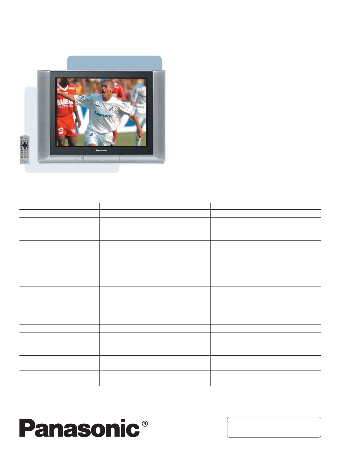
ORDER DCS - MAY2006 - 008LA - MS
Service Manual
TC-21FX30LA
TC-29FX30LA
TC-21FX30LP
TC-29FX30LP
Chassis GP41
Specifications
Model :
Power source :
Consumption :
Antenna IN/OUT jack :
Color system :
Channel capability :
Intermediate Frequency :
Audio and Video Terminals :
Input :
Output :
High Voltage :
Picture Tube :
Audio Output :
Dimensions (HxWxD)
Weight:
TC-21FX30LA / TC-21FX30LP
127V / 220V AC Auto, 50/60Hz
67W
75Ω - VHF / UHF / CATV
P AL-M / NTSC / P AL-N
VHF: 2 ~13 - UHF: 14 ~ 69 - CATV: 1 ~ 125
Video: 45,75 MHz
Audio: 41,25 MHz
Color: PAL-M: 3,575 MHz
PAL-N:3,582 MHz
NTSC: 3,579 MHz
DVD: AV1, AV2,DVD
Y: 1,0Vp-p, 75Ω
PB: 0,7Vp-p, 75Ω
PR: 0,7Vp-p, 75Ω
Audio: 400mVrms / Video: 1,0 Vp-p 75Ω
Audio: 400mVrms / Video: 1,0 Vp-p 75Ω
27,5 ± 1,5 kV (at zero beam current)
PANABLACK 21", 53 cm (NBR5258) 51cm
measured diagonally
8W + 8W (RMS)
648 x 472 x 488mm
23,8 kg
TC-29FX30LA / TC-29FX30LP
127V / 220V AC Auto, 50/60Hz
98W
75Ω - VHF / UHF / CATV
PAL-M / NTSC / PAL-N
VHF: 2 ~13 - UHF: 14 ~ 69 - CATV: 1 ~ 125
Video: 45,75 MHz
Audio: 41,25 MHz
Color: PAL-M: 3,575 MHz
PAL-N:3,582 MHz
NTSC: 3,579 MHz
DVD: AV1, AV2,DVD
Y: 1,0Vp-p, 75Ω
PB: 0,7Vp-p, 75Ω
PR: 0,7Vp-p, 75Ω
Audio: 400mVrms / Video: 1,0 Vp-p 75Ω
Audio: 400mVrms / Video: 1,0 Vp-p 75Ω
31,0 ± 1,5 kV (at zero beam current)
PANABLACK 29", 74 cm (NBR5258) 68 cm
measured diagonally
8W + 8W (RMS)
786 x 578 x 508mm
42,7 kg
Specifications are subject to change without prior notice.
Mass and dimensions shown are aproximated.
© 2006 Panasonic do Brasil Limitada
CS Division
Technical Support
Page 2

TC-21FX30LA/LP / TC-29FX30LA/LP
Important Safety Notice
Special components are used in this television set which are important for safety. These parts are identified on the schematic
diagram by the symbol . It is essential that these critical parts are replaced with the manufacturer’s specified replacement
parts to prevent X-ray radiation, shock, fire or other hazards. Do not modify the original design without manufacturer’s permission.
!
Contents
ABOUT LEAD FREE SOLDER (PbF) ............................................ 3
SUGGEST PbF SOLDER ............................................................... 3
HOW TO RECOGNIZE THA T PB FREE SOLDER IS USED ....... 3
SAFETY PRECAUTIONS ................................................................ 4
GP41 CHASSIS FEATURE SUMMAR Y ......................................... 5
IC601 - BLOCK DIAGRAM .............................................................. 6
IC601 - PINS DESCRIPTION ........................................................ 6
VOLT AGE T ABLES ........................................................................... 8
GP41 CHASSIS BLOCK DIAGRAM ............................................... 9
SERVICE HINTS .............................................................................. 10
FACTOR Y MODE ADJUSTMENT ................................................... 10
HOW TO OPERA TE THE CONTROLS IN SERVICE MODE ..... 1 1
HOW TO ACCESS THE MEMORY MAPS ................................... 12
COLOUR PURITY AND CONVERGENCE ADJUSTMENT ....... 20
CRT VRS ADJUSTMENT ................................................................ 22
RF AGC ADJUSTMENT ................................................................... 23
VIF DETECTOR OUTPUT LEVEL CONFIRMA TION .................. 23
BUZZING CONFIRMATION (AUDIO CIRCUIT) ........................... 23
ANODE AND HEA TER VOL T AGE CONFIRMATION ................... 23
PA L COLOR OUTPUT SIGNAL ADJUSTMENT ......................... 24
NTSC SUB-TINT CALIBRA TION ................................................... 24
PROTECTION CIRCUIT (SHUTDOWN) ...................................... 24
CONFIRMATION OF OPERA TION ................................................. 24
SUB-BRIGHT AND SUB-CONTRAST CALIBRATION ................ 25
FOCUS CALIBRATION .................................................................... 25
PURITY CALIBRA TION .................................................................. 25
WHITE QUALITY CALIBRATION .................................................... 26
CRT CUT OFF VOL TAGE ADJUST .............................................. 26
WHITE BALANCE CALIBRATION .................................................. 26
DEFLECTION CALIBRA TION AND CONFIRMA TION ................. 27
MAIN BOARD CIRCUIT LA YOUT .................................................. 29
“L” BOARD SCHEMATIC DIAGRAM (TC-21FX30LA / LP) ......... 30
“L” BOARD SCHEMATIC DIAGRAM (TC-29FX30LA / LP) ......... 31
“G” BOARD SCHEMATIC DIAGRAM (TC-29FX30LA / LP) ........ 32
“A” BOARD SCHEMATIC DIAGRAM (TC-21FX30LA / LP) ......... 33
“A” BOARD SCHEMATIC DIAGRAM (TC-29FX30LA / LP) ......... 34
WA VEFORM CHART ........................................................................ 35
EXPLODED VIEW ............................................................................ 38
MECHANICAL P ARTS LIST ........................................................... 39
ELECTRICAL P ARTS LIST (TC-21FX30LA/LP) ......................... 40
ELECTRICAL P ARTS LIST (TC-29FX30LA/LP) ......................... 44
General Guidelines
An Insulation Transformer should always be used during the
servicing of a receiver whose chassis is not insulated from the
AC power line. Use a transformer with adequate power rating
as its protects the technician from accidents resulting in personal
injury from electrical shocks. It will also protect the Receiver
from being damaged by accidental shorting that may occur
during servicing.
When servicing, observe the original lead dress, especially in
the high voltage circuit. Replace all damaged parts (also parts
that show signs of overheating.)
Always Replace Protective Devices, such as fishpaper,
insulation resistors and capacitors, and shields after servicing
the Receiver. Use only manufacturer’s recommended rating for
fuses, circuit breakers, etc.
High potentials are present when this Receiver is operating.
Operation of the Receiver without the rear cover introduces
danger from electrical shock. Servicing should not be performed
by anyone who is not thoroughly familiar with the necessary
precautions when servicing high-voltage equipment.
Extreme care should be practiced when Handling the Picture
Tube. Rough handling may cause it to implode due to
atmospheric pressure (14.7 lbs per sq. in). Do not sick or scratch
the glass or subject it to any undue pressure. When handling,
use safety goggles and heavy gloves for protection. Discharge
the picture tube by shorting the anode to chassis ground (not to
the cabinet or to other mounting hardware). When discharging
it, connect cold ground (i.e. dag ground lead) to the anode with
a well insulated wire or use a grounding probe.
Avoid prolonged exposure at close range to unshielded areas
of the picture tube to prevent exposure to X-ray radiation.
The Test Picture Tube used for servicing the chassis at the
bench should incorporate safety glass and magnetic shielding.
The safety glass provides shielding for the tube viewing area
against X-ray radiation as well as implosion. The magnetic
shield limits X-ray radiation around the bell of the picture tube in
addition to restricting magnetic effects. When using a picture
tube test jig for service, ensure that the jig is capable of handling
31kV without causing X-ray radiation.
Before returning a serviced receiver to the owner, the service
technician must thoroughly test the unit to ensure that is
completely safe to operate. Do not use a line insulation
transformer when testing.
Warning !
It is essential that these critical parts are replaced
with the manufacturer’s specified replacement parts
!
to prevent X-ray radiation, shock, fire or other hazards.
- 2 -
Page 3
TC-21FX30LA/LP / TC-29FX30LA/LP
ABOUT LEAD FREE SOLDER (PbF)
Note:
In the information below, Pb, the symbol for lead in the periodic table of elements, will refer to standard solder or solder that
contains lead.
We will use PbF solder when discussing the lead free solder used in our manufacturing process which is made from Tin (Sn),
Silver, (Ag), and Copper, (Cu).
This model, and others like it, manufactured using lead free solder will have PbF stamped on the PCB. For service and repair
work we suggest using the same type of solder although, with some precautions, standard Pb solder can also be used.
Caution
• PbF solder has a melting point that is 50° ~ 70° F, (30° ~ 40°C) higher than Pb solder. Please use a soldering iron with
temperature control and adjust it to 700° ± 20° F, (370° ± 10°C).In case of using high temperature soldering iron, please be
careful not to heat too long.
• PbF solder will tend to splash if it is heated much higher than its melting point, approximately 1100°F, (600°C).
• If you must use Pb solder on a PCB manufactured using PbF solder, remove much as possible the original PbF solder and be
sure that any remaining is melted prior to applying the Pb solder.
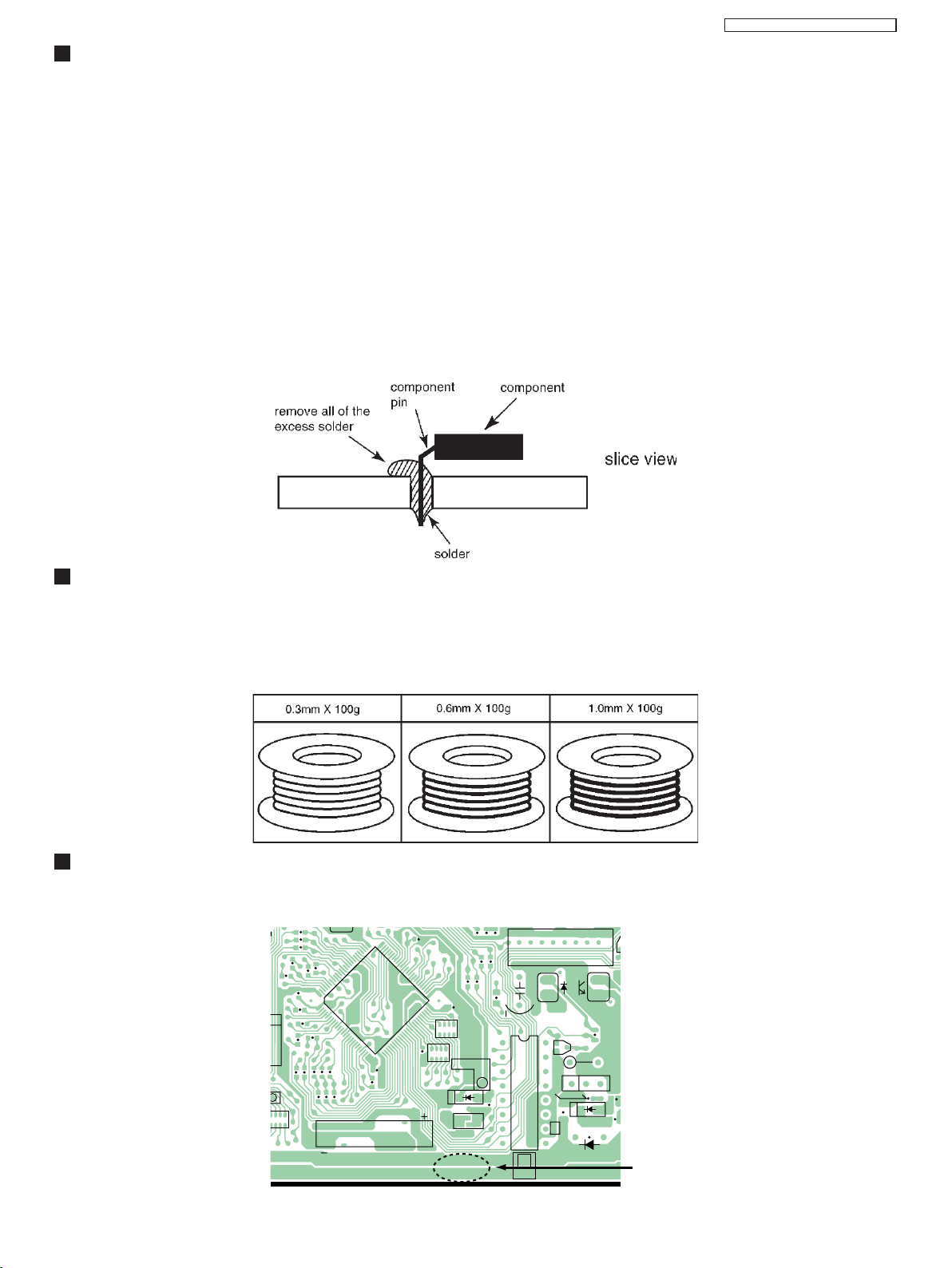
• When applying PbF solder to double layered boards, please check the component side for excess which may flow onto the
opposite side (See figure, below).
SUGGESTED PbF SOLDER
There are several types of PbF solder available commercially. While this product is manufactured using Tin, Silver, and Copper,
(Sn+Ag+Cu), you can also use Tin and Copper, (Sn+Cu), or Tin, Zinc, and Bismuth, (Sn+Zn+Bi). Please check the manufac
turer’s specific instructions for the melting points of their products and any precautions for using their product with other
materials.
The following lead free (PbF) solder wire sizes are recommended for service of this product: 0.3mm, 0.6mm and 1.0mm.
HOW TO RECOGNIZE THAT PB FREE SOLDER IS USED
P.C.Boards marked as “PbF” use Pb Free solder. (See the figure below.) Pb Free is not used the Power Supply Board of this
unit.
(Example : Digital Board)
L624
L625
L626
L660
L661
L658
L659
100
C694
L653
L655
L657
L654
L656
1
L642
R768
L605
H
RA602
PFUP1330YA PbF
R767
R769
L606
L604
Q609
75
76
IC605
2625
C666
L643
BAT600
R70
C738
51
50
C667
RA609
D602
C668
RA610
C672
C731
L620
L619
L618
+3.3V/BAT
J600
C717
L621
R723
L630
1
R708
8
C728
IC610
+24V
CN612
16
9
Q613
E
R736
F605
25
18
R613R610
R611
R737
E
Q620
D608
C726
D607
Marked
DIGITAL BOARD COMPONENT VIEW
- 3 -
Page 4
TC-21FX30LA/LP / TC-29FX30LA/LP
SAFETY PRECAUTIONS
General Guide Lines
1. It is advisable to insert an insulation transformer in the AC supply before servicing this hot chassis.
2. When servicing, observe the original lead dress, especially the lead dress in the high voltage circuits. If a short circuit is
found, replace all parts which have been overheated or damaged by the short circuit.
3. Af ter servicing, see to it that all the protective devices such as insulation barriers, insulation papers, shields and insulation
R-C combinations, are properly installed.
4. When the receiver is not to be used for a long period of time, unplug the power cord from the AC cord outlet.
5. Potential, as high as 29.0kV is present when this receiver is in operation. Operation of the receiver without the rear cover
involves the danger of a shock hazard from the receiver power supply . Servicing should not be attempted by anyone who
is not thoroughly familiar with the precautions necessary when working on high voltage equipment. Always discharge the
anode of the picture tube to the receiver chassis before handling the tube. After servicing make the following leakage
current checks to prevent the customer from being exposed to shock hazards.
Leakage Current Cold Check
1. Unplug the AC cord and connect a jumper between the two prongs on the plug.
2. Turn on the receiver’s power switch.
Measure the resistance value, with an ohmmeter , between the jumper AC plug and each exposed metallic cabinet part on
the receiver, such as screw heads, aerials, connectors, control shaft s, etc.When the exposed met allic part has a return
path to the chassis, the reading should be between 4M Ω. and 20M Ω. When the exposed metal does not have a return
path to the chassis, the reading must be infinite.
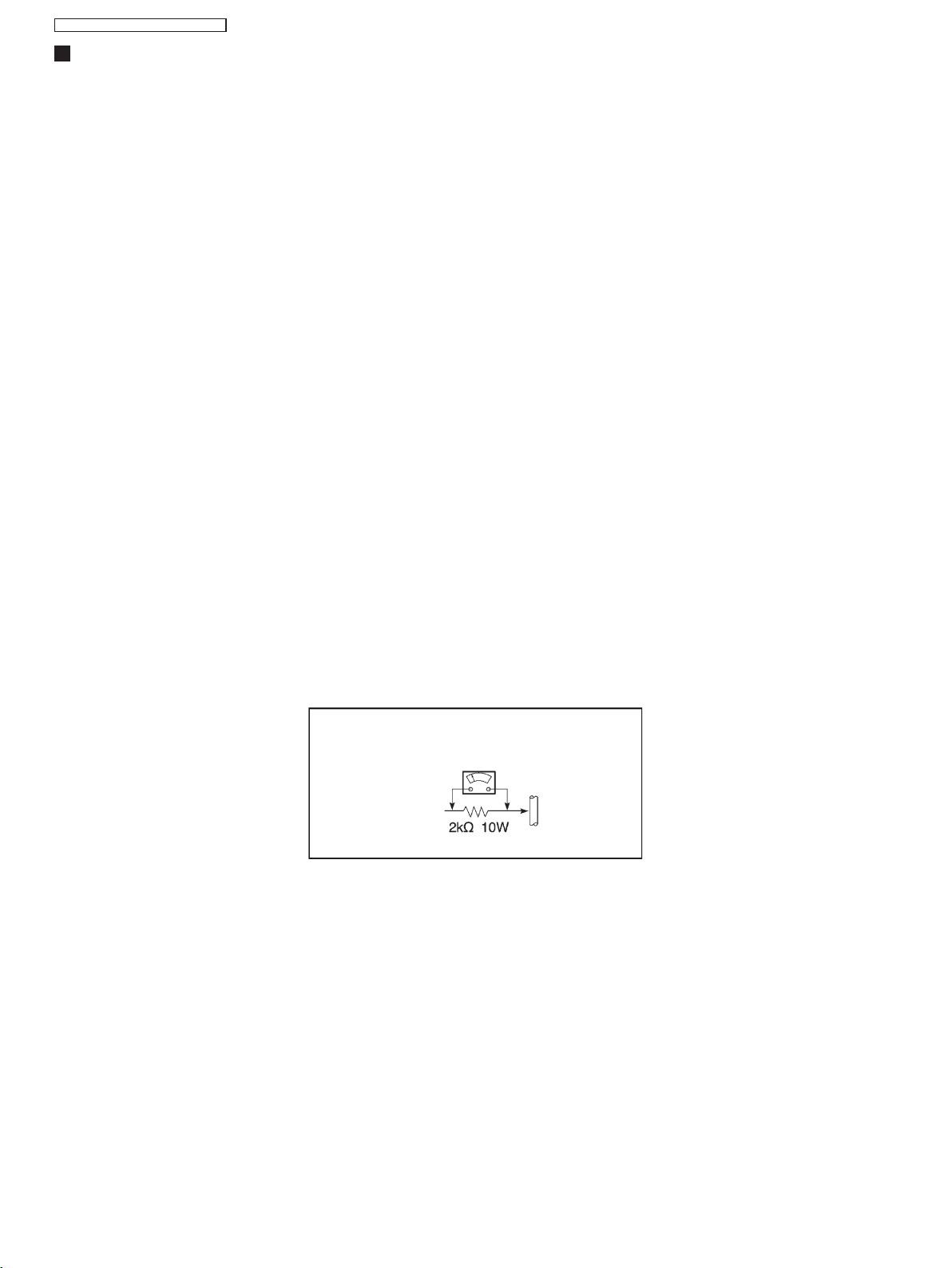
Leakage Current Hot Check (Fig. 1)
1. Plug the AC cord directly into the AC outlet. Do not use an insulation transformer for this check.
2. Use a non inductive 2KΩ 10W resistor in series with an exposed metallic part of the receiver and earth such as a water pipe.
3. Using a high impendance AC voltimeter , check the resistor’s potential.
4. Check each met allic part of the receiver .
5. Invert the plug of the AC chord and repeat all measurements .
6. The voltage from any point should not exceed 1.0V
. In case of a measurement is outside of these limits specified,
RMS
there is a possibility of a shock hazard and the receiver should be repaired and rechecked before it is returned to the
customer.
Hot - Check Circuit
AC Voltimeter
To
instrument’s
Metallic Parts
Exposet
Fig. 1
Water Pipe
(Earth)
X-Radiation
Warning:
The potential sources of X-Radiation in TV set are the EHT section and the picture tube. When using a picture tube test jig
for service, ensure that jig is capable of handling 29.0kV without causing X-Radiation.
Note: It is important to use an accurate periodically calibrated high voltage meter .
1. Set the brightness to minimum.
2. Use the remocon to get into Service Mode.
3. Measure the EHT. The meter reading should indicate 27.5±1.5kV. If the meter indication is out of tolerance, immediate
service and correction is required to prevent the possibility of premature component failure.
4. To prevent the possibility X-Radiation, it is essential to use the specified picture tube, if service replacement becomes
necessary.
- 4 -
Page 5
TC-21FX30LA/LP / TC-29FX30LA/LP
GP41 CHASSIS FEATURE SUMMARY
CHASSIS : GP41
MODEL : TC-21FX30LA, TC-21FX30LP, TC-29FX30LA and TC-29FX30LP
SYSTEM : 3 system (P AL-M/P AL-N/NTSC) (PAL-M 50Hz)
POWER SOURCE : CA automatic power switching (127/220)V, 50/60Hz
MEMORY : 125 positions
TV TUNING RANGE : 181 channels (TV / CA TV)
(OSD) LANGUAGE : Sp anish, Portuguese and English
AUDIO SYSTEM : Stereo MTS
VERTICAL MAGNETIC : -0.1 ±0.03 (BRAZIL)
COLOR TEMPERATURE : (High Light) x= 0.261±0.01, y=0.267 ±0.01, Y=150 (nit))
(Low Light) x= 0.247±0.01, y=0.273 ±0.01, Y=7.0 (nit)
REFERENCE VOLTAGE
CONTENTS TEST POINT
+B VOLTAGE
Sub-contrast
Anode (EHT) voltage
MEMORY DATA
TC-21FX30LA / LP
MEMORY DATA
TC-29FX30LA / LP
TPA15
TPA16
TPA17
TPA18
TPA19
TPA20
TPL5
CRT ANODE
OPTION 01 02 03 0 4 05 0 6 07 08 0 9 10 11 12 13 1 4 15
DA T A 36 00 02 01 00 10 02 0F 90 A1 00 00 00 08 05
OPTION 01 02 03 04 05 06 07 08 09 10 11 12 13 14 15
DA T A 36 00 02 01 00 10 02 0C 90 A1 00 00 00 08 05
TC-21FX30LA / LP
3,35 ± 0,2 (V)
141,0 ± 2,0 (V)
8,2 ± 0,3 (V)
1,9 ± 0,2 (V)
5,2 ± 0,2 (V)
175 ± 15 (V)
2,1 ±0.2Vo-p
27.5 ±1,5 (kV)
TC-29FX30LA / LP
3,35 ± 0,2 (V)
141,0 ± 2,0 (V)
8,2 ± 0,3 (V)
1,9 ± 0,2 (V)
5,2 ± 0,2 (V)
220 ± 15 (V)
2,3 ±0.2Vo-p
31,0 ±1,0 (kV)
- 5 -
Page 6
TC-21FX30LA/LP / TC-29FX30LA/LP
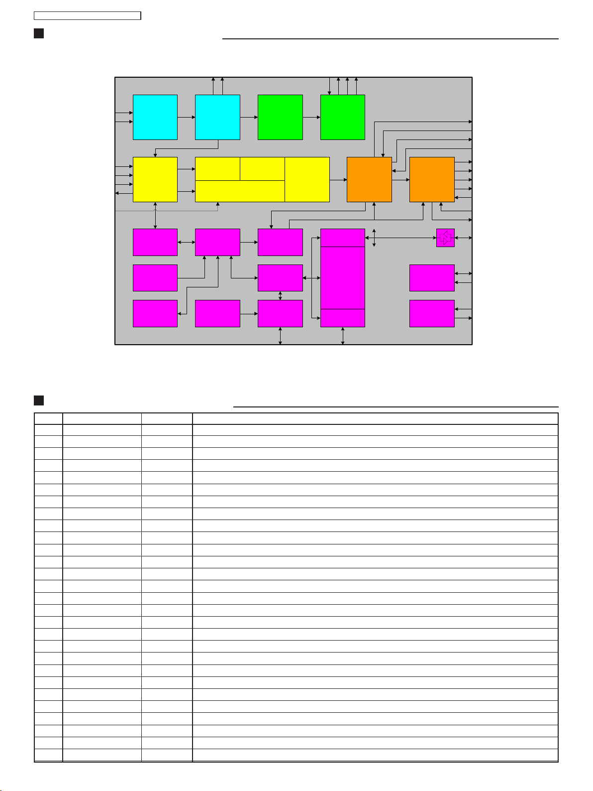
IC601 - BLOCK DIAGRAM
R
E
K
C
G
F
I
A
T
S
T
W
A
U
B
E
N
O
I
U
P
S
A
S
A
IFIN+
IFIN-
CVBS in
YCbCr in
RGB in
CVBS out
656 in
IF
Frontend
Video
Frontend
Slicer
24kB
Char ROM
20kB XRAM
IF
Processor
Comb
Filter
Component
Bus
Arbiter
256kB
Prog ROM
Interface
Sound
Demodulator
Color
Decoder
Display
Generator
CPU
8051
Memory
Interface
ADB, DB, PSENQ,
PSWEQ, WRQ, RDQ
Panorama
Scaler
Audio
Processor
I2C Master/
Slave
Timer
CRT
PWM
ADC
UART
Watchdog
RTC
I/O-Ports
Pxy
Display &
Deflection
Processor
Video
Backend
Reset & Test
Logic
Clock
Generator
656 out
PROT
HOUT
HFLB
VERT
EW
SVM
RGB out
RGB in
SENSE
RSW
I2C
RESETQ
TEST
XTAL1
XTAL2
IC601 - PINS DESCRIPTION
Pin
Symbol
1 GND SUPPLY Ground Platform
2 VSUP8.0AU SUPPLY Supply Voltage Analog Audio, 8.0 V
3 VREFAU Reference Voltage, Audio
4 SPEAKERL OUT Analog Loudspeaker Output, Left
5 SPEAKERR OUT Analog Loudspeaker Output, Right
6 AOUT1L OUT Analog Audio 1 Output, Left
7 AOUT1R OUT Analog Audio 1 Output, Right
8 AIN3L / AOUT2L IN / OUT Analog Audio 3 Input, Left
9 AIN3R / AOUT2R IN / OUT Analog Audio 3 Input, Right
10 AIN2L IN Analog Audio 2 Input, Left
11 AIN2R IN Analog Audio 2 Input, Right
12 AIN1L IN Analog Audio 1 Input, Left
13 AIN1R / SIF IN/OUT Analog Audio 1 Input, Right
14 TA G C OUT Tuner AGC Output
15 VREFIF Reference Voltage, IF ADC
16 IFIN- IN Differential IF Input
17 IFIN+ IN Differential IF Input
18 RESETQ IN/OUT Reset Input/Output
19 VSUP5.0FE SUPPLY Supply Voltage Analog IF Front-end, 5.0 V
20 VSUP5.0IF SUPPLY Supply Voltage IF ADC, 5.0 V
21 VSUP3.3DIG SUPPLY Supply Voltage Digital Core, 3.3 V
22 GND SUPPLY Ground Platform
23 GND SUPPLY Ground Platform
24 VSUP1.8DIG SUPPLY Supply Voltage Digital Core, 1.8 V
25 XTAL1 IN Analog Crystal Input
26 XTAL2 OUT Analog Crystal Output
27 P22 IN/OUT Port 2, Bit 2 Input/Output
28 P23 IN/OUT Port 2, Bit 3 Input/Output
Type
Description
- 6 -
Page 7

Pin Name Type Description
29 VIN11 IN Analog Video 11 Input
30 VIN10 IN Analog Video 10 Input
31 VIN9 IN Analog Video 9 Input
32 VIN8 IN Analog Video 8 Input
33 VIN7 IN Analog Video 7 Input
34 VIN6 IN Analog Video 6 Input
35 VIN5 IN Analog Video 5 Input
36 VIN4 IN Analog Video 4 Input
37 VIN3 IN Analog Video 3 Input
38 VIN2 IN Analog Video 2 Input
39 VIN1 IN Analog Video 1 Input
40 VOUT1 OUT Analog Video 1 Output
41 VOUT2 OUT Analog Video 2 Output
42 VOUT3 OUT Analog Video 3 Output
43 VSUP1.8FE SUPPLY Supply Voltage Analog Video Front-end, 1.8 V
44 GND SUPPLY Ground Platform
45 GND SUPPLY Ground Platform
46 VSUP3.3FE SUPPLY Supply Voltage Analog Video Front-end, 3.3 V
47 P10 IN/OUT Port 1, Bit 0 Input/Output
48 P11 IN/OUT Port 1, Bit 1 Input/Output
49 P12 IN/OUT Port 1, Bit 2 Input/Output
50 P13 IN/OUT Port 1, Bit 3 Input/Output
51 P14 IN/OUT Port 1, Bit 4 Input/Output
52 P15 IN/OUT Port 1, Bit 5 Input/Output
53 P16 IN/OUT Port 1, Bit 6 Input/Output
54 P17 IN/OUT Port 1, Bit 7 Input/Output
55 P20 IN/OUT Port 2, Bit 0 Input/Output
56 P21 IN/OUT Port 2, Bit 1 Input/Output
57 SCL IN/OUT I2C Bus Clock Input/Output
58 SDA IN/OUT I2C Bus Data Input/Output
59 VPROT IN Vertical Protection Input
60 HOUT OUT Horizontal Drive Output
61 HFLB IN Horizontal Flyback Input
62 SAFETY IN Safety Input
63 GNDDAC SUPPLY Ground Video DACs
64 VSUP3.3DAC SUPPLY Supply Voltage Video DACs, 3.3 V
65 VSUP3.3IO SUPPLY Supply Voltage I/O Ports, 3.3 V
66 GND SUPPLY Ground Platform
67 GND SUPPLY Ground Platform
68 VSUP3.3BE SUPPLY Supply Voltage Analog Video Back-end, 3.3 V
69 XREF Reference Current for RGB DACs
70 VRD Reference Voltage for RGB DACs
71 BOUT OUT Analog Blue Output
72 GOUT OUT Analog Green Output
73 ROUT OUT Analog Red Output
74 SVMOUT OUT Scan Velocity Modulation Output
75 BIN IN Analog Blue Input, Back-end
76 GIN IN Analog Green Input, Back-end
77 RI N IN Analog Red Input, Back-end
78 FBIN IN Fast Blank Input, Back-end
79 GNDM IN Reference Ground for Sense ADC
80 SENSE IN Sense ADC Input
81 RSW1 OUT Range Switch 1 Output
82 RSW2 OUT Range Switch 2 Output
83 EW OUT Vertical Parabola Output
84 VERT- OUT Differential Vertical Sawtooth Output
85 VERT+ OUT Differential Vertical Sawtooth Output
86 TEST / SUBW IN / OUT Test Input, reserved for Test Subwoofer Output
87 VSUP5.0BE SUPPLY Supply Voltage Analog Video Back-end, 5.0 V
88 GND SUPPLY Ground Platform
- 7 -
TC-21FX30LA/LP / TC-29FX30LA/LP
Page 8
TC-21FX30LA/LP / TC-29FX30LA/LP
VOLTAGE TABLES - TC-21FX30LA / LP
Pin Voltage
1 0
2 8,73
3 3,7
4 3,5
5 3,6
6 3,8
7 3,8
8 3,8
9 3,8
10 3,8
11 3,8
12 3,8
13 3,8
14 4,3
15 2,5
16 2,5
17 2,4
18 3,3
19 5,2
20 5,2
21 3,3
22 0
23 0
24 1,8
25 1,8
26 1,9
27 3,3
28 0
29 0
30 0
IC601
Pin Voltage
31 1,1
32 1,1
33 1,1
34 0
35 0
36 0
37 0
38 1
39 1
40 1
41 0
42 1,18
43 1,9
44 0
45 0
46 3,3
47 3,3
48 2,4
49 3,2
50 0
51 3,3
52 0
53 3,3
54 2,2
55 0
56 0
57 2
58 2,35
59 0
60 2,2
Pin Voltage
61 1,2
62 0
63 0
64 3,3
65 3,3
66 0
67 0
68 3,3
69 1,3
70 1,3
71 4,7
72 4,7
73 4,7
74 5,2
75 0
76 0
77 0
78 0
79 0
80 0
81 0
82 0
83 4,8
84 1,8
85 1,5
86 0
87 5,2
88 0
IC451
Pin Voltage
1 0,4V
2 13,6V
3 -13,5V
4 -13,6V
5 8,6V
6 14V
7 0,5V
IC857
Pin Voltage
1 1,3V
20V
3 4,8V
4 5,2V
5 3,3V
IC1101
Pin Voltage
10V
20V
30V
40V
5 2,6V
62V
70V
8 3,3V
IC801
Pin Voltage
1 200V
2 0,2V
3 21,5V
4 2,0V
5 0,2V
6 1,3V
7 1,8V
IC871
Pin Voltage
1 4,3V
26V
30V
4 3,3V
5 1,3V
IC2301
Pin Voltage
1 14,5V
20V
30V
40V
5 5,2
60V
7 15,5V
8 7,1V
9 7,1V
10 0V
11 7,5V
12 7,2V
13 0V
IC802
Pin Voltage
1 142V
2 7,2V
30V
IC875
Pin Voltage
1 1,3V
20V
3 3,1V
4 3,4V
52V
XF101
Pin Voltage
1 0,15V
2 0,15V
3
4 2,54V
5 2,25V
TEST
POINTS
TPA11
16,5V
TPA16
142V
IC851
Pin Voltage
1 2,8V
2 7,5V
30V
4 4,7V
50V
T801
Pin Voltage
1 0,22V
2 18,8V
3NC
4NE
5 206V
6 180V
7 180V
8NC
9 170V
10 15V
11 16,5V
12 0V
13 10V
14 6,5V
15 0V
16 0V
17 NC
18 142V
VOLTAGE TABLES - TC-29FX30LA / LP
Pin Voltage
1 0
2 8,73
3 3,7
4 3,5
5 3,6
6 3,8
7 3,8
8 3,8
9 3,8
10 3,8
11 3,8
12 3,8
13 3,8
14 4,3
15 2,5
16 2,5
17 3,3
18 3,3
19 5,2
20 5,2
21 3,3
22 0
23 0
24 1,8
25 1,8
26 1,9
27 3,3
28 0
29 0
30 0
IC601
Pin Voltage
31 1,1
32 1,1
33 1,1
34 1,1
35 1,1
36 0
37 0
38 1,1
39 1,1
40 1,1
41 0
42 0
43 1,9
44 0
45 0
46 3,3
47 3,3
48 2,4
49 3,2
50 0
51 3,3
52 0
53 3,3
54 2,2
55 0
56 0
57 3
58 0
59 0
60 2,2
Pin Voltage
61 1,2
62 0
63 0
64 3,3
65 3,3
66 0
67 0
68 3,3
69 1,3
70 1,3
71 4,7
72 4,7
73 4,7
74 4,3
75 0
76 0
77 0
78 0
79 0
80 0
81 0
82 0
83 4,8
84 1,8
85 1,5
86 0
87 5,2
88 0
IC451
Pin Voltage
1 0,4V
2 15,4V
3 -13,5V
4 -14V
5 9,9V
6 16,8V
7 0,5V
IC857
Pin Voltage
1 1,3V
20V
3 4,8V
4 5,2V
5 3,3V
IC1101
Pin Voltage
10V
20V
30V
40V
5 2,6V
6 2,3V
70V
8 3,3V
- 8 -
IC801
Pin Voltage
1 200V
2 0,2V
3 21,5V
4 3,7V
5 1,5V
6 0,7V
7
IC871
Pin Voltage
1 4,3V
2 5,1V
30V
4 3,3V
5 1,3V
IC2301
Pin Voltage
1 14,5V
20V
30V
40V
5 5,2
60V
7 15,5V
8 7,1V
9 7,1V
10 0V
11 7,5V
12 7,2V
13 0V
IC802
Pin Voltage
1 142V
2 7,2V
30V
IC875
Pin Voltage
1 1,3V
20V
3 3,1V
4 3,4V
52V
XF101
Pin Voltage
1 0,15V
2 0,15V
3
4 2,54V
5 2,25V
TEST
POINTS
TPA11
16,5V
TPA16
142V
IC851
Pin Voltage
1 3,3V
2 5,1V
30V
4 5,1V
5 1,3V
T801
Pin Voltage
1 0,22V
2 22V
3NC
4NE
5 206V
6 180V
7 180V
8NC
9 170V
10 15V
11 16,5V
12 0V
13 10V
14 6,5V
15 0V
16 0V
17 NC
18 142V
All voltage measurements were made
in POWER ON mode, with 127V 60Hz
power source and Color Bars Video
Pattern.
Page 9
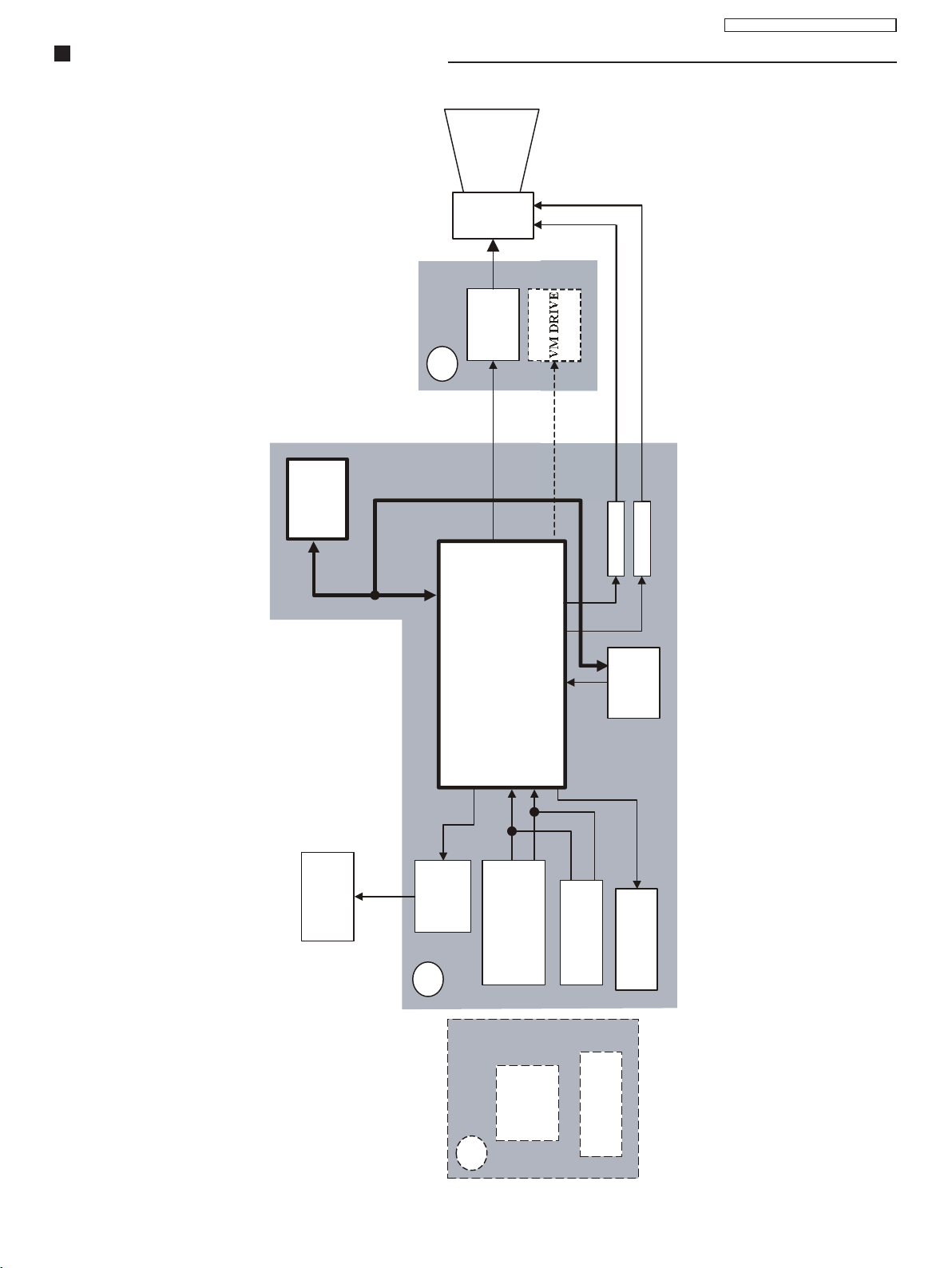
GP41 CHASSIS BLOCK DIAGRAM
TC-21FX30LA/LP / TC-29FX30LA/LP
CRT
coil
defl.
CRT
DRIVE
L
VM DRIVE
IC1101
EEPROM
SPEAKER
SCL SDA
R/G/B
CVBS OUT
AMP
AUDIO
A
RGB
OUT
AUDIO
IC2301
IC601
VCT-IF
V_IN
REAR INPUTS
AV1 : V/L/R
AV3 : YUV/V/L/R
_IN
A
VM
V
H
IF
MON_OUT
AV2 : V/L/R
FRONT INPUTS
V OUT
H OUT
TUNER
V/L/R
MON_OUT
- 9 -
MAIN
POWER
SWITCH
G
AV2 : V/L/R
FRONT INPUTS
Page 10
TC-21FX30LA/LP / TC-29FX30LA/LP
SERVICE HINTS
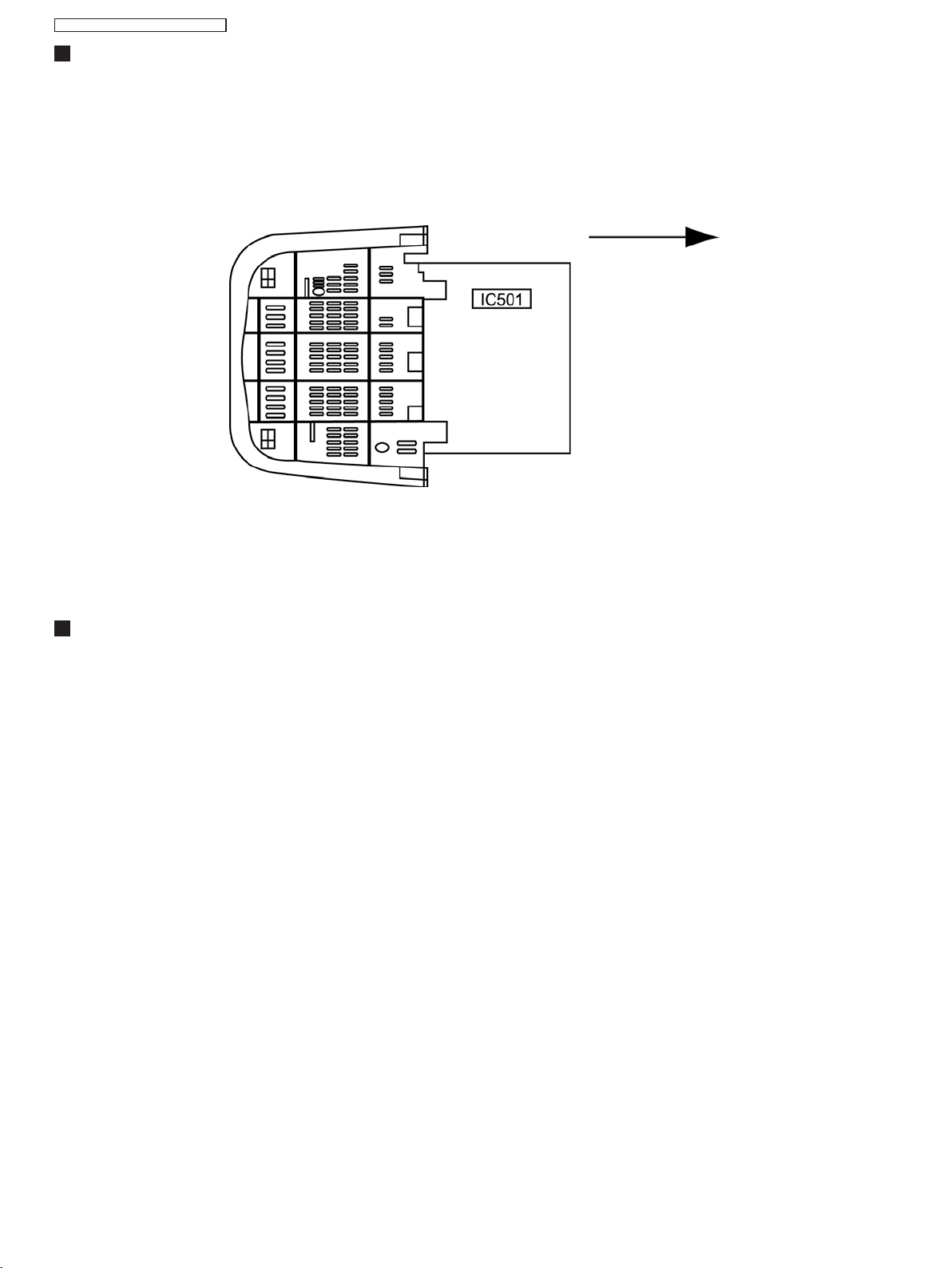
SERVICE POSITION FOR E-BOARD
1. Remove the back cover.
2. Stand the TV set as shown in Fig. 2.
3. Remove the A-Board from the TV set by pulling the main board out as shown in Figure 2.
Pull out this way
Main Board
Fig. 2
FACTORY MODE ADJUSTMENT (TC-21FX30LA/LP / TC-29FX30LA/LP)
HOW TO ENTER IN THE GP41 SERVICE MODE:
TO ENTER IN THE SERVICE MODE 1:
à
1. Adjust “OFF TIMER” to 30 minutes.
Press simultaneously “VOLUME (–)” on the front panel and “RECALL” on the remote control to enter “SERVICE MODE-1”.
TO ENTER IN THE SERVICE MODE 2:
à
1. Enter in the “SERVICE MODE 1”.
2. Press the “1” channel key to enter “SERVICE MODE 2”.
TO ENTER IN THE SERVICE MODE 3:
à
1. Enter in the “SERVICE MODE 2”.
2. Press the “1” channel key to enter “SERVICE MODE 3”.
Note: Always, finishing the adjustments, press the “NORMAL” key or the “POWER” key in the remote control to exit the
service mode and return to TV normal way .
- 10 -
Page 11
TC-21FX30LA/LP / TC-29FX30LA/LP
How to operate the controls in the SERVICE MODE 1
à
Key 3 / 4 Previous / next item
Key 8 / 9 Ajusts bright (user) (–/+)
UP/DOWN Channel Up / Channel Down
Volume + Increment of selected item
Volume – Decrement of selected item
OK Store / saves selected item
Normal Exit the service mode
Obs: The vertical and horizontal deflection adjustments, in the SERVICE
MODE 1, was made in 50Hz power source frequency.
How to operate the controls in the SERVICE MODE 2
à
Key 3 / 4 Previous / next item
Key 8 / 9 Select bit 0–7 option
UP/DOWN Channel Up / Channel Down
Volume + Increment of selected item
Volume – Decrement of selected item
OK Store / saves selected item
Normal Exit the service mode
SERVICE MODE 1
ITEM
H-POS
V-POS
H-AMP
V-AMP
EW-AMP1
DVCO
R High
B High
R Low
B Low
SubBrightness
SERVICE MODE 2
ITEM
Y/C DELAY
OPTION 1
OPTION 2
OPTION 3
OPTION 4
OPTION 5
OPTION 6
OPTION 7
OPTION 8
OPTION 9
OPTION 10
OPTION 1 1
OPTION 12
OPTION 13
OPTION 14
OPTION 15
21”
-14
-43
-----42
-----63
0379
0409
0157
0211
29
21”
-3
36
00
02
01
00
10
00
0F
90
A1
00
00
00
08
05
29”
9
-43
6
29
-23
-63
0406
0396
0035
0097
39
29”
-1
36
00
02
01
00
10
02
0C
90
A1
00
00
00
08
05
How to operate the controls in the SERVICE MODE 3
à
Key 3 / 4 Previous / next item
UP/DOWN Channel Up / Channel Down
Volume + Increment of selected item
Volume – Decrement of selected item
OK Store / saves selected item
Normal Exit the service mode
Note: Always, finishing the adjustments, press the “NORMAL” key or the “POWER” key in the remote control to leave
the service mode and return to TV normal way .
- 11 -
H-POS 60Hz Offs
V-POS 60Hz Offs
H-AMP 60Hz Offs
V-AMP 60Hz Of fs
EW-AMP1 60Hz Offs
Low Corner
Trapez 1
Upper corner
V-LIN
V-SYM
ANGLE
BOW
VZOOM
SERVICE MODE 3
ITEM 21”
-16
4
---17
----
----
----
----
-8
28
-2
2
255
29”
-4
11
-2
-6
1
1
-1
5
-8
27
-1
-2
256
Page 12
TC-21FX30LA/LP / TC-29FX30LA/LP
How to access the Memory Maps (TC-21FX30LA / LP, TC-29FX30LA / LP)
à
1. Select SET UP – SYNTONY – ANTENNA – CABLE
2. Select the channel 99
3. Enter in the SERVICE MODE 2.
4. press “RECALL” in the remote control.
5. “MEMORY EDIT” appears in the screen.
6. Use the "1" or "2" key to move the cursor in the
horizontal direction and the "3" or "4" key to move the
∧∧
∧
7. The “
∧∧
time.
8. The bytes are adjusted one by one through the
“VOLUME +” and “VOLUME–” keys.
9. Press the “OK” key to store each adjusted byte.
10. Press the “NORMAL” or “POWER” key to exit the
“MEMORY EDIT MODE”.
” and “
∨∨
∨
∨∨
” channel key changes the page one by
cursor in the vertical direction.
TC-21FX30LA/LP
TC-21FX30LA / LP - TABLE A0
COLUMN
COLUMN COLUMN COLUMN COLUMN COLUMN COLUMN COLUMN COLUMN COLUMN COLUMN COLUMN COLUMN COLUMN COLUMN COLUMN
+0 +1 +2 +3 +4 +5 +6 +7 +8 +9 +A +B +C +D +E +F
LINE
000 BD 10 00 00 04 00 00 00 00 00 00 00 00 00 00 46
LINE
010 36 00 02 01 00 10 02 0F 90 A1 00 00 00 08 05 00
LINE
020 80 00 06 00 81 00 06 00 82 00 06 00 83 00 06 00
LINE
030 84 00 06 00 85 00 06 00 86 00 86 09 87 00 06 00
LINE
040 88 10 06 00 89 00 06 00 8A 10 06 00 8B 00 06 00
LINE
050 8C 00 06 00 8D 00 06 00 8E 00 06 00 8F 10 06 00
LINE
060 90 00 06 00 91 00 06 00 92 00 06 00 93 00 06 00
LINE
070 94 00 06 00 95 00 06 00 96 00 06 00 97 00 06 00
LINE
080 98 00 06 00 99 00 06 00 9A 00 06 00 9B 00 06 00
LINE
090 9C 10 06 00 9D 00 06 00 9E 00 06 00 9F 10 06 00
LINE
0A0 A0 00 06 00 A1 00 06 00 A2 00 06 00 A3 00 06 00
LINE
0B0 A4 00 06 00 A5 00 06 00 A6 00 06 00 A7 00 06 00
LINE
0C0 A8 00 06 00 A9 00 06 00 A A 00 06 00 AB 00 06 00
LINE
0D0 AC 00 06 00 AD 00 06 00 AE 00 06 00 AF 00 06 00
LINE
0E0 B0 00 06 00 B1 00 06 00 B2 00 06 00 B3 00 06 00
LINE
0F0 B4 00 06 00 B5 00 06 00 B6 00 06 00 B7 00 06 00
TC-21FX30LA / LP - TABLE A2
COLUMN COLUMN COLUMN COLUMN COLUMN COLUMN COLUMN COLUMN COLUMN COLUMN COLUMN COLUMN COLUMN COLUMN COLUMN COLUMN
+0 +1 +2 +3 +4 +5 +6 +7 +8 +9 +A +B +C +D +E +F
LINE
100 B8 00 06 00 B9 00 06 00 BA 00 06 00 BB 00 06 00
LINE
110 BC 00 06 00 BD 00 06 00 BE 00 06 00 BF 00 06 00
LINE
120 C0 00 06 00 C1 00 06 00 C2 00 06 00 C3 00 06 00
LINE
130 C4 00 86 F6 C5 00 06 00 C6 00 86 F6 C7 00 06 00
LINE
140 C8 00 06 00 C9 00 06 00 CA 00 06 00 CB 00 06 00
LINE
150 CC 00 06 00 CD 00 06 00 CE 00 06 00 CF 00 06 00
LINE
160 D0 00 06 00 D1 00 06 00 D2 00 06 00 D3 00 06 00
LINE
170 D4 00 06 00 D5 00 06 00 D6 00 06 00 D7 00 06 00
LINE
180 D8 00 06 00 D9 00 06 00 DA 00 06 00 DB 00 06 00
LINE
190 DC 00 06 00 DD 00 06 00 DE 00 06 00 DF 00 06 00
LINE
1A0 E0 00 06 00 E1 00 06 00 E2 00 06 00 E3 00 06 00
LINE
1B0 E4 00 06 00 E5 00 06 00 E6 00 06 00 E7 00 06 00
LINE
1C0 E8 00 06 00 E9 00 06 00 EA 00 06 00 EB 00 06 00
LINE
1D0 EC 00 86 F6 ED 00 06 00 EE 00 06 00 EF 00 06 00
LINE
1E0 F0 00 06 00 F1 00 06 00 F2 00 06 00 F3 00 06 00
LINE
1F0 F4 00 06 00 F5 00 06 00 F6 00 06 00 F7 00 06 00
- 12 -
Page 13

TC-21FX30LA/LP / TC-29FX30LA/LP
TC-21FX30LA / LP - TABLE A4
COLUMN COLUMN
COLUMN COLUMN COLUMN COLUMN COLUMN COLUMN COLUMN COLUMN COLUMN COLUMN COLUMN COLUMN COLUMN COLUMN
+0 +1 +2 +3 +4 +5 +6 +7 +8 +9 +A +B +C +D +E +F
LINE
200 F8 00 06 00 F9 00 06 00 FA 00 06 00 FB 00 06 00
LINE
210 FC 00 06 00 FD 00 06 00 01 00 02 00 00 02 01 18
LINE
220 20 03 00 07 00 00 00 00 00 00 00 00 00 00 00 00
LINE
230 00 00 01 02 00 04 FF 64 FF 00 00 00 00 00 00 00
LINE
240 06 06 06 06 00 00 00 00 00 00 00 00 01 00 00 00
LINE
250 00 00 00 00 00 00 00 00 00 00 00 00 00 00 00 00
LINE
260 00 00 00 00 00 00 00 00 00 00 00 00 00 00 00 00
LINE
270 00 00 00 00 FF FF FF FF FF FF FF FF FF 00 00 00
LINE
280 00 00 00 00 00 00 00 00 00 00 00 00 00 00 00 00
LINE
290 00 00 00 00 00 00 00 00 00 00 00 00 00 00 00 00
LINE
2A0 18 00 18 00 00 00 00 00 18 00 18 00 00 00 64 32
LINE
2B0 32 10 32 01 46 32 2D 06 32 01 37 32 2D 02 32 01
LINE
2C0 64 32 32 10 32 01 46 32 2D 06 32 01 37 32 2D 02
LINE
2D0 32 01 64 32 32 10 32 01 46 32 2D 06 32 01 37 32
LINE
2E0 2D 02 32 01 64 32 32 10 32 01 46 32 2D 06 32 01
LINE
2F0 37 32 2D 02 32 01 64 32 32 10 32 01 46 32 2D 06
TC-21FX30LA / LP - TABLE A6
COLUMN COLUMN COLUMN COLUMN COLUMN COLUMN COLUMN COLUMN COLUMN COLUMN COLUMN COLUMN COLUMN COLUMN COLUMN COLUMN
+0 +1 +2 +3 +4 +5 +6 +7 +8 +9 +A +B +C +D +E +F
LINE
300 32 01 37 32 2D 02 32 01 00 46 32 2D 06 32 01 00
LINE
310 37 32 2D 02 32 01 00 0F 0B 09 13 17 08 10 13 10
LINE
320 0C 0F 0B 09 0D 14 0A 0D 0D 0B 09 0C 0C 0C 0C 0C
LINE
330 00 04 04 05 00 0B 04 0A 06 07 00 00 00 00 00 00
LINE
340 50 A5 00 00 00 00 00 A5 64 FF FF 25 00 00 00 00
LINE
350 00 00 FF 00 00 0A A0 02 0D 40 0A 10 00 00 00 00
LINE
360 00 00 10 12 01 88 01 01 04 01 01 09 04 04 01 0D
LINE
370 00 F2 09 04 0A 04 01 00 07 04 0A 07 20 1D DC 05
LINE
380 A0 00 07 00 05 00 00 00 00 00 00 02 00 18 00 03
LINE
390 00 01 02 00 00 00 00 00 64 32 32 08 32 01 46 32
LINE
3A0 2D 06 32 01 37 32 2D 02 32 01 00 00 00 0F 0B 09
LINE
3B0 13 17 08 10 13 10 0C 0F 0B 09 0D 14 0A 0D 0D 0B
LINE
3C0 09 0C 0C 0C 0C 0C 00 04 04 05 00 0B 04 0 A 06 07
LINE
3D0 00 00 00 01 00 00 00 00 00 00 10 01 01 10 21 03
LINE
3E0 01 00 10 01 01 10 21 03 01 00 10 01 01 10 21 03
LINE
3F0 01 00 10 01 01 10 21 03 01 00 10 01 01 10 21 03
- 13 -
Page 14

TC-21FX30LA/LP / TC-29FX30LA/LP
TC-21FX30LA / LP - TABLE A8
COLUMN COLUMN
COLUMN COLUMN COLUMN COLUMN COLUMN COLUMN COLUMN COLUMN COLUMN COLUMN COLUMN COLUMN COLUMN COLUMN
+0 +1 +2 +3 +4 +5 +6 +7 +8 +9 +A +B +C +D +E +F
LINE
400 01 00 10 01 01 10 21 03 01 00 10 01 01 10 21 03
LINE
410 01 00 10 01 01 10 21 03 01 00 10 01 01 10 21 03
LINE
420 01 00 10 01 01 10 21 03 01 00 10 01 01 10 21 03
LINE
430 01 00 10 01 01 10 21 03 01 00 10 01 01 10 21 03
LINE
440 01 00 10 01 01 10 21 03 01 00 10 01 01 10 21 03
LINE
450 01 00 10 01 01 10 21 03 01 00 10 01 01 10 21 03
LINE
460 01 00 10 01 01 10 21 03 01 00 10 01 01 10 21 03
LINE
470 01 00 10 01 01 10 21 03 01 00 10 01 01 10 21 03
LINE
480 01 00 10 01 01 10 21 03 01 00 10 01 01 10 21 03
LINE
490 01 00 10 01 01 10 21 03 01 00 10 01 01 10 21 03
LINE
4A0 01 00 00 9D 00 F2 00 D3 01 7B 01 6D 01 99 67 C0
LINE
4B0 1B BC 1C 01 15 02 F8 02 E9 FE 30 30 30 30 E6 E6
LINE
4C0 E6 E6 0C 0C 0C 0C 01 01 01 01 0F 0F 0F 0F FE 00
LINE
4D0 FE FC 02 04 01 03 E5 01 F1 FB FC E0 30 FC FF FE
LINE
4E0 FC FF FD FF 00 00 06 04 00 2D 80 00 C4 00 C0 00
LINE
4F0 07 05 0B 00 02 02 02 6A 6 A 6A 00 27 81 27 81 12
TC-21FX30LA / LP - TABLE AA
COLUMN COLUMN COLUMN COLUMN COLUMN COLUMN COLUMN COLUMN COLUMN COLUMN COLUMN COLUMN COLUMN COLUMN COLUMN COLUMN
+0 +1 +2 +3 +4 +5 +6 +7 +8 +9 +A +B +C +D +E +F
LINE
500 01 90 00 12 01 06 05 3F 21 21 22 21 37 00 FC 00
LINE
510 FF FE 02 02 00 00 00 14 FC FC 2A 00 2A 00 FC 03
LINE
520 FC 03 FC 03 BC 02 BC 02 BC 02 BC 02 0C 00 06 02
LINE
530 02 32 FB 2D 04 18 00 14 04 18 00 14 04 18 02 11
LINE
540 0E 08 0F 0F 0F 02 02 00 00 F0 01 03 02 02 02 2A
LINE
550 44 42 40 3E 3 A 36 30 20 10 01 40 3E 3C 38 34 30
LINE
560 28 1C 10 01 00 00 00 11 00 0B 0B 0B 0B 0B 08 0B
LINE
570 0B 0B 07 05 07 07 07 07 01 03 E0 FA F8 F7 F8 F7
LINE
580 F5 F2 EF EC EB 02 00 FF 00 FF F E FC FA F7 F3 00
LINE
590 01 02 03 04 00 01 02 04 00 00 00 00 00 06 00 00
LINE
5A0 04 00 02 00 00 04 00 47 26 26 26 3B 3B 3B 6B 21
LINE
5B0 6C 28 00 00 01 F4 01 01 00 FA FD 00 00 00 07 B2
LINE
5C0 01 50 09 00 00 7C 01 FF FF 21 3F 37 37 01 C3 81
LINE
5D0 81 D8 D8 18 04 C5 1F 04 C5 18 04 05 18 83 E4 05
LINE
5E0 13 47 00 94 07 67 02 03 18 10 10 11 11 36 80 19
LINE
5F0 1C 00 00 08 07 3C 3F 77 00 05 FA 07 FC 07 FC 07
- 14 -
Page 15
TC-21FX30LA/LP / TC-29FX30LA/LP
TC-21FX30LA / LP - TABLE AC
COLUMN COLUMN
COLUMN COLUMN COLUMN COLUMN COLUMN COLUMN COLUMN COLUMN COLUMN COLUMN COLUMN COLUMN COLUMN COLUMN
+0 +1 +2 +3 +4 +5 +6 +7 +8 +9 +A +B +C +D +E +F
LINE
600 FD 05 FC 07 40 C0 03 00 00 02 00 0D C0 F7 C0 06
LINE
610 00 FA FA 11 3F 70 01 60 01 40 FF C0 00 40 FF 50
LINE
620 00 DD FF 23 00 00 10 1B 00 40 40 01 10 05 00 00
LINE
630 80 00 80 04 50 00 00 00 00 60 06 00 00 00 00 00
LINE
640 00 00 00 0F 00 03 50 01 40 01 3C 81 40 02 58 37
LINE
650 C0 37 C0 37 C0 02 58 B5 00 00 07 00 00 0B 00 00
LINE
660 03 E8 0F 03 0F 0F 00 18 03 F5 00 18 00 18 00 7D
LINE
670 00 64 00 82 00 82 03 EC 03 F4 03 EC 03 EC 03 E2
LINE
680 03 D2 03 E2 03 E2 00 78 00 74 00 78 00 78 03 E7
LINE
690 03 FC 03 E7 03 E7 F6 01 F6 F6 01 F6 01 F6 F6 BC
LINE
6A0 BC 12 11 35 3C 35 3C 02 70 F0 F8 00 9A 01 25 24
LINE
6B0 23 1E FF FF FF FF 41 3D 39 0B C0 C0 C0 C0 E0 1F
LINE
6C0 09 04 00 00 06 3E 0E 00 40 00 40 00 00 3E 00 3E
LINE
6D0 0E 00 0E 00 0E 00 0E 00 32 01 FF 00 12 0F 2B 01
LINE
6E0 FB 00 19 12 A0 00 06 00 00 00 00 00 00 00 00 00
LINE
6F0 00 00 00 00 00 00 00 02 02 B8 40 02 80 FB 00 F0
TC-21FX30LA / LP - TABLE AE
COLUMN COLUMN COLUMN COLUMN COLUMN COLUMN COLUMN COLUMN COLUMN COLUMN COLUMN COLUMN COLUMN COLUMN COLUMN COLUMN
+0 +1 +2 +3 +4 +5 +6 +7 +8 +9 +A +B +C +D +E +F
LINE
700 C0 E6 80 E1 80 14 40 00 00 00 00 D0 04 D0 04 C6
LINE
710 00 C6 00 D0 04 D0 04 C6 00 C6 00 69 05 C1 55 00
LINE
720 FF FE 00 00 00 19 00 00 4A B9 4B FA 00 00 00 00
LINE
730 00 00 00 00 00 02 04 FF FF FF FF FF FF FF FF FF
LINE
740 FF FF FF FF FF FF FF FF FF FF FF FF FF FF FF FF
LINE
750 FF FF FF FF FF FF FF FF FF FF FF FF FF FF FF FF
LINE
760 FF FF FF FF FF FF FF FF FF FF FF FF FF FF FF FF
LINE
770 FF FF FF FF FF FF FF FF FF FF FF FF FF FF FF FF
LINE
780 FF FF FF FF FF FF FF FF FF FF FF FF FF FF FF FF
LINE
790 FF FF FF FF FF FF FF FF FF FF FF FF FF FF FF FF
LINE
7A0 FF FF FF FF FF FF FF FF FF FF FF FF FF FF FF FF
LINE
7B0 FF FF FF FF FF FF FF FF FF FF FF FF FF FF FF FF
LINE
7C0 FF FF FF FF FF FF FF FF FF FF FF FF FF FF FF FF
LINE
7D0 FF FF FF FF FF FF FF FF FF FF FF FF FF FF FF FF
LINE
7E0 FF FF FF FF FF FF FF FF FF FF FF FF FF FF FF FF
LINE
7F0 FF FF FF FF FF FF FF FF FF FF FF FF FF FF FF FF
- 15 -
Page 16

TC-21FX30LA/LP / TC-29FX30LA/LP
TC-29FX30LA / LP
TC-29FX30LA / LP - TABLE A0
COLUMN COLUMN
COLUMN COLUMN COLUMN COLUMN COLUMN COLUMN COLUMN COLUMN COLUMN COLUMN COLUMN COLUMN COLUMN COLUMN
+0 +1 +2 +3 +4 +5 +6 +7 +8 +9 +A +B +C +D +E +F
LINE
000 00 00 00 00 00 00 00 00 00 00 00 00 00 00 00 30
LINE
010 36 00 02 01 00 10 02 0C 90 A1 00 00 00 08 05 00
LINE
020 80 03 06 00 81 03 06 00 82 03 06 00 83 03 06 00
LINE
030 84 03 06 00 85 03 06 00 86 03 06 00 87 03 06 00
LINE
040 88 03 06 00 89 03 06 00 8A 13 06 00 8B 03 06 00
LINE
050 8C 0B 06 00 8D 03 06 00 8E 03 06 00 8F 03 06 00
LINE
060 90 03 06 00 91 03 06 00 92 03 06 00 93 03 06 00
LINE
070 94 03 06 00 95 03 06 00 96 03 06 00 97 03 06 00
LINE
080 98 03 06 00 99 03 06 00 9A 03 06 00 9B 03 06 00
LINE
090 9C 13 06 00 9D 03 06 00 9E 03 06 00 9F 13 06 00
LINE
0A0 A0 03 06 00 A1 03 06 00 A2 03 06 00 A3 03 06 00
LINE
0B0 A4 03 06 00 A5 03 06 00 A6 03 06 00 A7 03 06 00
LINE
0C0 A8 03 06 00 A9 03 06 00 A A 03 06 00 AB 03 06 00
LINE
0D0 AC 03 06 00 AD 03 06 00 AE 03 06 00 AF 03 06 00
LINE
0E0 B0 03 06 00 B1 03 06 00 B2 03 06 00 B3 03 06 00
LINE
0F0 B4 03 06 00 B5 03 06 00 B6 03 06 00 B7 03 06 00
TC-29FX30LA / LP - TABLE A0
COLUMN COLUMN COLUMN COLUMN COLUMN COLUMN COLUMN COLUMN COLUMN COLUMN COLUMN COLUMN COLUMN COLUMN COLUMN COLUMN
+0 +1 +2 +3 +4 +5 +6 +7 +8 +9 +A +B +C +D +E +F
LINE
100 B8 03 06 00 B9 0B 06 00 BA 03 06 00 BB 03 06 00
LINE
110 BC 03 06 00 BD 03 06 00 BE 03 06 00 BF 03 06 00
LINE
120 C0 03 06 00 C1 03 06 00 C2 03 86 09 C3 03 06 00
LINE
130 C4 03 86 F6 C5 03 06 00 C6 03 06 00 C7 03 06 00
LINE
140 C8 03 06 00 C9 03 06 00 CA 03 06 00 CB 03 06 00
LINE
150 CC 03 06 00 CD 03 06 00 CE 03 06 00 CF 03 06 00
LINE
160 D0 03 06 00 D1 03 06 00 D2 03 06 00 D3 03 06 00
LINE
170 D4 03 06 00 D5 03 06 00 D6 03 86 09 D7 03 06 00
LINE
180 D8 03 06 00 D9 03 06 00 DA 03 06 00 DB 03 06 00
LINE
190 DC 03 06 00 DD 03 06 00 DE 03 06 00 DF 03 06 00
LINE
1A0 E0 03 06 00 E1 03 06 00 E2 03 06 00 E3 03 06 00
LINE
1B0 E4 03 06 00 E5 03 06 00 E6 03 06 00 E7 03 06 00
LINE
1C0 E8 03 06 00 E9 03 06 00 EA 03 06 00 EB 03 86 09
LINE
1D0 EC 03 06 00 ED 03 06 00 EE 03 06 00 EF 03 06 00
LINE
1E0 F0 03 06 00 F1 03 06 00 F2 03 06 00 F3 03 06 00
LINE
1F0 F4 03 06 00 F5 03 06 00 F6 03 06 00 F7 03 06 00
- 16 -
Page 17

TC-21FX30LA/LP / TC-29FX30LA/LP
TC-29FX30LA / LP - TABLE A4
COLUMN COLUMN
COLUMN COLUMN COLUMN COLUMN COLUMN COLUMN COLUMN COLUMN COLUMN COLUMN COLUMN COLUMN COLUMN COLUMN
+0 +1 +2 +3 +4 +5 +6 +7 +8 +9 +A +B +C +D +E +F
LINE
200 F8 03 06 00 F9 03 06 00 FA 03 06 00 FB 03 06 00
LINE
210 FC 03 06 00 FD 03 06 00 01 00 02 00 00 00 01 18
LINE
220 20 03 00 07 00 00 00 00 00 00 00 00 00 00 00 00
LINE
230 00 00 01 02 00 04 FF 64 FF 00 00 00 00 00 00 00
LINE
240 06 06 06 06 00 00 00 00 00 00 00 00 01 00 00 00
LINE
250 00 00 00 00 00 00 00 00 00 00 00 00 00 00 00 00
LINE
260 00 00 00 00 00 00 00 00 00 00 00 00 00 00 00 00
LINE
270 00 00 00 00 FF FF FF FF FF FF FF FF FF 00 00 00
LINE
280 00 00 00 00 00 00 00 00 00 00 00 00 00 00 00 00
LINE
290 00 00 00 00 00 00 00 00 00 00 00 00 00 00 00 00
LINE
2A0 18 00 18 00 00 00 00 00 18 00 18 00 00 00 64 32
LINE
2B0 32 06 32 01 46 32 2D 03 32 01 37 32 2D 01 32 01
LINE
2C0 64 32 32 06 32 01 46 32 2D 03 32 01 37 32 2D 01
LINE
2D0 32 01 64 32 32 06 32 01 46 32 2D 03 32 01 37 32
LINE
2E0 2D 01 32 01 64 32 32 06 32 01 46 32 2D 03 32 01
LINE
2F0 37 32 2D 01 32 01 64 32 32 06 32 01 46 32 2D 03
TC-29FX30LA / LP - TABLE A2
COLUMN COLUMN COLUMN COLUMN COLUMN COLUMN COLUMN COLUMN COLUMN COLUMN COLUMN COLUMN COLUMN COLUMN COLUMN COLUMN
+0 +1 +2 +3 +4 +5 +6 +7 +8 +9 +A +B +C +D +E +F
LINE
300 32 01 37 32 2D 01 32 01 03 46 32 2D 06 32 01 03
LINE
310 37 32 2D 03 32 01 03 13 0B 0A 13 17 08 10 13 10
LINE
320 0C 0F 0B 09 0D 14 0A 0D 0D 0B 09 0C 0C 0C 0C 0C
LINE
330 01 04 04 05 00 0B 04 0A 06 07 03 03 03 03 00 01
LINE
340 30 A5 0C 03 8C 43 DA A5 64 FF FF 25 00 00 50 00
LINE
350 00 00 FF 00 00 0D A 0 05 0F 40 0A 10 00 00 00 00
LINE
360 00 00 10 12 01 88 01 01 04 01 01 09 04 04 01 0D
LINE
370 00 C8 09 04 0A 04 01 00 07 04 0A 07 20 1D DC 05
LINE
380 A0 00 07 00 05 00 00 00 00 00 00 02 00 18 00 03
LINE
390 00 01 02 00 00 00 00 00 64 32 32 06 32 01 46 32
LINE
3A0 2D 03 32 01 37 32 2D 01 32 01 00 00 00 13 0B 0A
LINE
3B0 13 17 08 10 13 10 0C 0F 0B 09 0D 14 0A 0D 0D 0B
LINE
3C0 09 0C 0C 0C 0C 0C 01 04 04 05 00 0B 04 0 A 06 07
LINE
3D0 00 00 00 01 00 00 00 00 00 00 10 01 01 10 21 03
LINE
3E0 01 00 10 01 01 10 21 03 01 00 10 01 01 10 21 03
LINE
3F0 01 00 10 01 01 10 21 03 01 00 71 02 01 06 10 99
- 17 -
Page 18
TC-21FX30LA/LP / TC-29FX30LA/LP
TC-29FX30LA / LP - TABLE A8
COLUMN COLUMN
COLUMN COLUMN COLUMN COLUMN COLUMN COLUMN COLUMN COLUMN COLUMN COLUMN COLUMN COLUMN COLUMN COLUMN
+0 +1 +2 +3 +4 +5 +6 +7 +8 +9 +A +B +C +D +E +F
LINE
400 01 00 10 01 01 10 21 03 01 00 10 01 01 10 21 03
LINE
410 01 00 10 01 01 10 21 03 01 00 10 01 01 10 21 03
LINE
420 01 00 10 01 01 10 21 03 01 00 10 01 01 10 21 03
LINE
430 01 00 10 01 01 10 21 03 01 00 10 01 01 10 21 03
LINE
440 01 00 10 01 01 10 21 03 01 00 10 01 01 10 21 03
LINE
450 01 00 10 01 01 10 21 03 01 00 10 01 01 10 21 03
LINE
460 01 00 10 01 01 10 21 03 01 00 10 01 01 10 21 03
LINE
470 01 00 10 01 01 10 21 03 01 00 10 01 01 10 21 03
LINE
480 01 00 10 01 01 10 21 03 01 00 10 01 01 10 21 03
LINE
490 01 00 10 01 01 10 21 03 01 00 10 01 01 10 21 03
LINE
4A0 01 00 00 45 00 87 00 78 01 6F 01 63 01 95 1D C2
LINE
4B0 F A D9 1B 1D 1A 17 F8 F6 F8 E E 06 05 FE FF E9 F1
LINE
4C0 01 F3 01 03 03 01 FF 02 FF FF 05 07 04 02 FF FF
LINE
4D0 00 FD FE 05 02 05 D5 FE 0B 13 09 FC 28 FC FF FE
LINE
4E0 FC FF FD FF 1E 00 05 04 00 35 80 00 C3 00 C2 00
LINE
4F0 07 05 0B 00 02 02 02 6A 6 A 6A 00 27 81 27 81 43
TC-29FX30LA / LP - TABLE A9
COLUMN COLUMN COLUMN COLUMN COLUMN COLUMN COLUMN COLUMN COLUMN COLUMN COLUMN COLUMN COLUMN COLUMN COLUMN COLUMN
+0 +1 +2 +3 +4 +5 +6 +7 +8 +9 +A +B +C +D +E +F
LINE
500 01 90 00 43 01 06 05 3F 21 21 22 21 37 00 FC 00
LINE
510 FF FE 02 02 00 00 00 14 F9 F9 2 A 00 2A 00 FC 03
LINE
520 FC 03 FC 03 BC 02 BC 02 BC 02 BC 02 0C 00 06 02
LINE
530 02 32 FB 2D 04 18 00 14 04 18 00 14 04 18 02 11
LINE
540 0E 08 0F 0F 0F 02 02 FF 00 F0 FE FE FE 02 02 2A
LINE
550 40 3B 38 36 33 30 28 20 10 01 3C 38 34 32 30 2C
LINE
560 24 1C 10 01 00 00 00 11 00 0B 0B 0B 0B 0B 08 0B
LINE
570 0B 0B 07 05 07 07 07 07 01 03 E0 FA F8 F7 F8 F7
LINE
580 F5 F2 EF EC EB 02 00 FF 00 FF F E FC FA F7 F3 00
LINE
590 00 00 00 00 00 01 02 04 00 00 00 00 00 06 00 00
LINE
5A0 04 00 02 00 00 04 00 47 26 26 26 6B 3B 3B 3B 21
LINE
5B0 6C 27 00 00 03 F4 02 00 00 FE 00 00 00 00 07 C0
LINE
5C0 01 79 0E 1D 00 7C 01 00 32 81 39 37 37 01 C3 81
LINE
5D0 81 D8 D8 18 04 C5 1F 04 C5 18 04 05 18 83 E4 05
LINE
5E0 13 47 00 94 07 67 02 03 18 10 10 11 11 36 80 19
LINE
5F0 1C 00 00 08 07 3C 3F 77 00 05 03 03 03 03 03 03
- 18 -
Page 19

TC-21FX30LA/LP / TC-29FX30LA/LP
TC-29FX30LA / LP - TABLE AC
COLUMN COLUMN
COLUMN COLUMN COLUMN COLUMN COLUMN COLUMN COLUMN COLUMN COLUMN COLUMN COLUMN COLUMN COLUMN COLUMN
+0 +1 +2 +3 +4 +5 +6 +7 +8 +9 +A +B +C +D +E +F
LINE
600 03 03 03 03 03 00 0F 00 00 02 00 0D C0 F7 C0 06
LINE
610 00 FA FA 07 3F 90 01 E0 01 40 FF C0 00 30 FF 60
LINE
620 00 AB FE 55 01 00 14 1D 00 40 40 01 10 05 00 00
LINE
630 80 00 80 04 50 01 0C 0C 0C 60 00 00 00 06 06 14
LINE
640 02 02 00 0F 00 00 10 01 AA 01 D9 12 C0 00 B4 25
LINE
650 80 25 80 2F 80 02 BC CE 00 00 00 00 00 0B 01 02
LINE
660 06 E8 0F 03 0F 0F 00 18 03 F5 00 18 00 18 00 82
LINE
670 00 64 00 82 00 82 03 EC 03 F4 03 EC 03 EC 03 E2
LINE
680 03 D2 03 E2 03 E2 00 78 00 74 00 78 00 78 03 E7
LINE
690 03 FC 03 E7 03 E7 F6 03 F6 F6 01 F6 01 F6 F6 BC
LINE
6A0 BC 12 11 37 37 37 37 02 70 F0 F8 00 9A 01 25 24
LINE
6B0 23 1E FF FF FF FF 41 3D 39 0B C0 C0 C0 C0 E0 1F
LINE
6C0 09 04 00 00 06 3E 0E 00 40 00 40 00 00 3E 00 3E
LINE
6D0 0E 00 0E 00 0E 00 0E 00 30 01 FF 00 13 0F 2B 01
LINE
6E0 FA 00 19 13 B4 00 06 00 00 00 00 00 00 00 00 00
LINE
6F0 00 00 00 00 00 00 00 00 02 B8 40 02 80 F0 80 F4
TC-29FX30LA / LP - TABLE AE
COLUMN COLUMN COLUMN COLUMN COLUMN COLUMN COLUMN COLUMN COLUMN COLUMN COLUMN COLUMN COLUMN COLUMN COLUMN COLUMN
+0 +1 +2 +3 +4 +5 +6 +7 +8 +9 +A +B +C +D +E +F
LINE
700 00 A0 80 B4 80 00 00 00 00 00 00 E7 04 DC 04 DC
LINE
710 00 C8 00 D0 04 D0 04 C6 00 C6 00 A9 08 C1 39 01
LINE
720 00 FE 00 00 00 00 00 00 00 00 00 00 81 81 81 02
LINE
730 81 81 81 02 4C 02 04 FF FF FF FF FF FF FF FF FF
LINE
740 FF FF FF FF FF FF FF FF FF FF FF FF FF FF FF FF
LINE
750 FF FF FF FF FF FF FF FF FF FF FF FF FF FF FF FF
LINE
760 FF FF FF FF FF FF FF FF FF FF FF FF FF FF FF FF
LINE
770 FF FF FF FF FF FF FF FF FF FF FF FF FF FF FF FF
LINE
780 FF FF FF FF FF FF FF FF FF FF FF FF FF FF FF FF
LINE
790 FF FF FF FF FF FF FF FF FF FF FF FF FF FF FF FF
LINE
7A0 FF FF FF FF FF FF FF FF FF FF FF FF FF FF FF FF
LINE
7B0 FF FF FF FF FF FF FF FF FF FF FF FF FF FF FF FF
LINE
7C0 FF FF FF FF FF FF FF FF FF FF FF FF FF FF FF FF
LINE
7D0 FF FF FF FF FF FF FF FF FF FF FF FF FF FF FF FF
LINE
7E0 FF FF FF FF FF FF FF FF FF FF FF FF FF FF FF FF
LINE
7F0 FF FF FF FF FF FF FF FF FF FF FF FF FF FF FF FF
- 19 -
Page 20

TC-21FX30LA/LP / TC-29FX30LA/LP
Before Colour Purity , Convergence and White Balance adjustment are attempted,
V. Height, H. Centre and Focus adjustments must be completed.
Colour Purity
1. Set the Brightness and Contrast controls to their maximum
positions.
2. Operate the TV set for 60 minutes.
3. Fully degausse the picture tube by using an external
degaussing coil.
4. Apply a crosshatch pattern signal and adjust the static
convergence magnets to the approximately correct position.
5. Receive a black and white signal.
6. Set the control as follows:
Red................minimum
Green.............minimum
Blue...............minimum
Press the Shipping button on the remote control twice to
select CRT Adjustment Mode to select low light.
7. Loosen the clamp screw for the Deflection Yoke A in Fig.
10 and move the Deflection Yoke as close to the purity
magnet as possible.
8. Adjust the purity magnetic rings so that a vertical green
field is obtained at the centre of the screen.
Colour Purity
Green
Convergence
1. Apply a crosshatch p attern signal and Normalize Contrast
control to the maximum positions.
2. Adjust Brightness until the grey position of the crosshatch
pattern just becomes black.
3. Adjust the Red and Blue line at the centre of the screen by
rotating the R-B static.
Vertical
Convergence
Red & Blue
Horizontal
Convergence
Red 7 Blue
Slide magnetic tabs toward or away
from each other.
R-B Static
Convergence Magnet
Totate both magnetic rings together
R-B Static
Convergence magnet
Purit magnet
Fig.5
Green Field
9. Slowly push the Deflection Y oke and set it where a uniform
green field is obtained.
Uniform
Green
Fig.6
10. Re-adjust the Low Light controls to their correct settings
and make sure that a uniform white field is obtained.
1 1. Tighten the clamp screw A in Fig. 10.
Fig.7
4. Adjust Red and Blue with Green line at centre of the screen
by rotating (RB)-G static convergence magnetic rings.
5. Lock convergence magnets with silicone sealer.
6. Remove the DY wedges and slightly tilt the Deflection Y oke
vertically and horizontally to obtain the good overall
convergence.
Fig.8
7. Fix the Deflection Yoke by reinserting the DY wedges.
Refer to Fig. 10.
8. If purity error is found, repeat “Colour Purity” adjustment.
- 20 -
Page 21

CRT
TC-21FX30LA/LP / TC-29FX30LA/LP
R-B Static
Convergence Magnet
Clamp for Convergence &
Puritymagnet
Deflection Yoke
Wedge A
Purety Magnet
Fig.11
Wedge C
(R-B)-G Static
Convergence Magnet
Wedge B
Fig.12
Notes:
1. Wedge A, B and C should be inserted following the sequence of 1, 2 and 3 shown in Fig. 12.
2. The wedges should be set 120° apart from each other .
3. Be certain that three wedges are firmly fixed and the Deflection Yoke is tightly clamped in place.
Otherwise the Deflection Yoke may shift its position and cause a loss of convergence and purity.
- 21 -
Page 22

TC-21FX30LA/LP / TC-29FX30LA/LP
CRT VRS ADJUSTMENT
1. Preparation
a. Set DY to CRT not to tilt up and down left and right deflection.
b. Set CY to CRT and set CY magnet primarily (Fig. 9)
Purity magnet : Set purity magnet that 2 magnets are (TOP POSITION)
VRS magnet : Set purity magnet 2 magnets are (HORIZONTAL POSITION)
2. Aajustiment
a. Receive that Cross Hatch pattern.
b. Adjust V-SHIFT -50Hz.
c. Set 2 magnets of horizontal position to up and down equally so that it will be the center part of CRT. (Fig. 10)
VRS Mg.
Pur Mg.
CRT Side
4 pole
Fig.9
Fig.10
6 pole
Purity set to top
(vertical)
*VRS set to
horizontal pos
- 22 -
Page 23

ADJUSTMENTS
ITEM / PREPARATION PROCEDURE
TC-21FX30LA/LP / TC-29FX30LA/LP
1- RF AGC ADJUSTMENT
1. Supply a color bar PHILIPS pattern and adjust the RF
input signal of 69 dB mV (75W opened channel 7 RF
freq.: 175.25 MHz).
2. Connect the digital multimeter in TPA15.
ADJUSTMENT:
1. Select “RF AGC” on “CHK2” service mode.
2. Adjust "RF AGC" by pressing VOL(+) or (-) until obtaining
2.2±0.1V in TPA15.
3. Increase the input level by +2 dB and confirm that the
voltage decreases in TPA15.
2- VIF DETECTOR OUTPUT LEVEL CONFIRMATION CONFIRMATION:
1. Install the chassis in the VIF calibration JIG and tune in a
63 dBU colorbar pattern (75Ω opened).
2. Connect the oscilloscope in TPA31.
3. Confirm that the output video sign is 1.05 ± 0.15 Vp-p in
TPA 31.
3- BUZZING CONFIRMATION (AUDIO CIRCUIT)
1. Connect the oscilloscope with a 7KHz filter between A222 and A22-3 speakers terminals .
Set the controls as follows:
Volume ................Maximum
Balance ............. Center
Surround ............ OFF
Hyper Bass ........ OFF
AVL ......................OFF
Sound Menu ......Dialog
CONFIRMATION:
1. Supply a colorbar signal with local frequency adjusted
and the AFC ON (Channel with sound bearer and without
modulation).
2. Assure that the width in the buzzing waveform is smaller
than 500 m Vp-p.
smaller than
500 m Vp-p
4- ANODE AND HEATER VOLTAGE CONFIRMATION
1. Supply a crosshatch signal.
2. Adjust the current beam to zero. (0 beam).
3. Adjust “SCREEN VR” and “CONTRAST” to minimum.
Note:
(When using a high voltage meter resistive type, it is
necessary to use an electrostatic meter type to verify the
values)
CONFIRMATION
1. Connect a voltage meter between TPA10 and ground.
Confirm that the voltage +B is within a range of 140.5V±
1.5V
2. Connect a high frequency voltage meter (VRMS) among
the heater, and confirm that the voltage is according to
the table below:
21" 6,30 ± 0,25 Vrms
29" Flat 6,30 ± 0,25 Vrms
3. Connect the high voltage meter in the CRT anode pin,
and confirm that the high voltage is be among 25,2~23KV
for 14” CRT and 27,2~25KV for 20" CRT .
- 23 -
Page 24

TC-21FX30LA/LP / TC-29FX30LA/LP
ADJUSTMENTS
ITEM / PREPARATION PROCEDURE
5- PAL COLOR OUTPUT SIGNAL ADJUSTMENT
1. Supply a color bar signal and adjust the local frequency.
2. Adjust “IMAGE” to DYNAMIC NORMAL, “CONTRAST” to
63 and “SUB-CONTRAST” to 21.
3. Adjust the “CHANNEL COLOR” level to NORMAL.
4. Set to CHK2 service mode option, press “5” on the remote
control unit and confirm that OSD becomes blue (AKB
turned off).
5. Set ABL to OFF (in CHK2 mode, to access BRT, CONT,
S-CONT or S-TINT).
6. Adjust [A] for 2.3 ± 0.2V through the BRIGHT control
variation in the test point TPL2.
RGB CONTRAST - 4DAC
{ 352 } - 14H
7. Confirm that the RGB Contrast is 11DAC and {352} = 1B
8. Fix G-DRIVE GAIN, R-DRIVE GAIN and B-DRIVE GAIN
data in 1FH or 31 DAC.
R-DRIVE GAIN: [SLV(8A), SUB (16)]
G-DRIVE GAIN: [SLV(8A), SUB (17)]
B-DRIVE GAIN: [SLV(8A), SUB (18)]
6- NTSC SUB-TINT CALIBRA TION
1. Connect the oscilloscope in TPL1 (R-OUT) with a 10KΩ
resistor.
2. Supply a Rainbow signal (NTSC 3.58 MHz) through
VIDEO IN.
3. Select “IMAGE” to DYNAMIC NORMAL.
4. Select “COLOR FOR CHANNEL” to NORMAL.
5. On CHK2 service mode, press “5” (AKB OFF) and confirm
that OSD becomes blue (AKB turned off).
6. Set ABL to OFF (on CHK2 mode, to access BRT, CONT,
S-CONT or S-TINT).
CALIBRATION:
1. Connect the oscilloscope in TPL2 (G-OUT) with a 10KΩ
resistor and adjust “CONTRAST”, so that the [B] waveform
it is 2.3±0.5V with 14” CRT and 2.6±0.1V with 20” CRT.
2. Adjust “SUB-COLOR” to obtain 2,45±0.5V in [D]
according to fig. 1.
3. Connect the oscilloscope in TPL1 (R-OUT) with a 10KΩ
resistor and confirm that the [C] waveform it is 2.45±0.5V
according to fig. 2.
4. Press the key “5” (AKB ON) and confirm that OSD
becomes white.
Fig. 1
A = 2.0 ±0.2Vo-p
B = 2.3±0.5V
D = 2.15±0.5V
Fig. 2
A = 2.0 ±0.2Vo-p
C = 2.5±0.5V
CALIBRATION:
1. Adjust [C] for 5.0±0.2V through the BRIGHT control
variation (CHK2) according to fig. 1.
2. Adjust SUB TINT-NTSC so that the levels of positions 2, 3
and 4 of Fig. 1 in accordance with the Fig. 2.
3. Set ABL to ON.
4. Press “5” and confirm that OSD becomes white (AKB
turned on).
7- PROTECTION CIRCUIT (SHUTDOWN)
CONFIRMATION OF OPERA TION
1. Supply a crosshatch pattern signal and adjust the
CONTRAST and BRIGHT DAC controls to minimum.
(Ibeam=0 μA)
Fig. 1 Fig. 2
CONFIRMATION:
1. Connect the voltmeter in TPA22 and confirm that the
voltage is smaller than [A].
2. Connect a DC source in TPA22 and confirm that the
protection circuit doesn't act when the voltage is [B].
3. Confirm that the protection circuit acts with smaller voltage
than [C].
Condition
A
B
C
21” Samsung
22,8
23,9
26,7
21” Philips
23,3
24,5
27,4
29” flat
23,2
24,1
27,0
4. Use D512 catode or C511 (+) terminal, if TP22 access it
is difficult.
- 24 -
Page 25

ADJUSTMENTS
ITEM / PREPARATION PROCEDURE
TC-21FX30LA/LP / TC-29FX30LA/LP
8- SUB-BRIGHT AND SUB-CONTRAST
CALIBRATION
1. Supply a WINDOW pattern signal.
2. Adjust IMAGE MENU to DYNAMIC NORMAL
9- FOCUS CALIBRATION
• Assure that the SUB-BRIGHTNESS adjustment has been
done.
1. Supply a Philips or monoscope pattern signal.
2. Adjust IMAGE MENU to DYNAMIC NORMAL.
SUB-BRIGHT CALIBRATION
1. Position the color analyzer in the LOW LIGHT image
area.
2. Ajust S-BRT <CHK 4> control, so that it is Y=0,7±0,2.
SUB-CONTRAST CALIBRA TION
1. Position the color analyzer in the HIGH LIGHT image
area.
2. Ajust S-CONT <CHK 4> DAC control, so that it is
Y=230±10 for 20” CRT and Y=380±20 for 14” CRT.
3. If impossible to obtain that adjustment, adjust SUBCONT <CHK 4> again.
4. Check the SUB-BRIGHT adjust.
CALIBRATION:
1. Adjust the FOCUS variable resistor for the point of better
adjustment.
• with PHILIPS signal .... take as reference for adjustment
the third vertical line (fig. 1).
• with MONOSCOPE signal in the number 4 (fig.2).
4
1 2 3
Fig. 1
3 2 1
10- PURITY CALIBRA TION
1. Adjust the HELMHOLTZ device for the local magnetic field
(HORIZONTAL: 0 ± 0.03 X 10⁻⁴T)
2. Let the set warm up (aging time) for a minimum of 60
minutes.
3. Supply a purity pattern (white pattern).
4. Adjust CONTRAST and BRIGHT to MAXIMUM.
5. The static convergence adjustment must have been
made preliminarily.
6. Connect a DC ampere meter between FBT pin11 (-) and
FBT pin3 (+), and adjust to 920μA±10%, varying the SBRT DAC control.
CRT
21”
29”
[*A]
10μm ±5
0μm ±5
Fig. 2
CALIBRA TION:
1. Position the “ears” of the purity magnets both upward.
2. Adjust the purity until the markers in the purity jig
monitorscope becomes symmetrical in the horizontal
direction.
3. The vertical centralization correction is made through
the purity magnets for stripe CRT type only.
4. Slide the yoke forward by 10 mm±5 in the monitor. Then,
tighten the deflection yoke.
5. Repeat the procedures 2 ~ 3 ~ 4.
6. Press the belt of deflection yoke.
7. Adjust “beam landing” using a microscope. (for model
change or instrument check only)
- 25 -
Page 26

TC-21FX30LA/LP / TC-29FX30LA/LP
ADJUSTMENTS
ITEM / PREPARATION PROCEDURE
WHITE QUALITY CALIBRA TION
PREPARATION:
1. Adjust the HELMHOLTZ device to local magnetic field. Horizontal: 0 ± 0.003 x 10
-4
T
2. Receive a white purity pattern.
3. Adjust CONTRAST and BRIGHT controls to maximum.
4. Previously adjust the CONVERGENCE.
5. Fully degauss the CRT by using an external degaussing
coil.
CRT CUT OFF VOLTAGE ADJUST
Important: Use proof tip x100 in the CRT cathode.
1. Connect the proof tip in the “G” cathode (“L” P.C.B.).
2. Supply a WINDOW pattern signal.
3. Select picture menu: DYNAMIC NORMAL
4. Adjust SUB-BRIGHTNESS in 0 (zero).
CALIBRATION:
1. Adjust the magnetic field in 0.4x10⁻⁴T (400 mG), and
check the white quality with the CRT turned to EAST and
to WEST .
2. Receive a red pattern, adjust the COLOR control to
maximum and confirm the purity adjustment.
3. If purity error is found at the CRT corners, apply magnetic
tapes to correct it, fully degauss the CRT again and repeat
the steps 1 and 2. Don't use this magnetic tapes on the
internal side of the yoke.
4. When magnetic tapes be used, fully degauss the face of
CRT (in a horizontal magnetic field = 0 ± 0.03x10⁻⁴T),
and repeat the items 1 and 2.
5. Adjust the control of COLOR to MINIMUM, and repeating
the item 1.
CALIBRA TION:
1. Set CUT OFF data as below:
Model (CRT) 21” 29”
R,G,B CUT OFF 242 135
2. Adjust the screen trimpot to obtain in the “G” cathode the
voltage (* V) es below (fig.1).
Model (CRT) 21” 29”
*V 150 180
*V
Fig. 1
WHITE BALANCE CALIBRA TION
CALIBRATION:
A) LOW LIGHT CALIBRATION
1. Adjust the HELMHOLTZ device to local magnetic field.
2. Let the set warm up for a minimum of 30 minutes.
3. Receive a white balance. (This sign should contain
burst sign).
4. Adjust the IMAGE menu to DINÂMIC NORMAL.
5. Fully degauss the CRT by using an external degaussing
coil.
6. Position the color analyzer in contact with the CRT face.
7. Access the SERVICE MODE 1
1. Adjust S-BRT, so that Y = 7
2. Adjust B-CUT OFF, so that x = 0,247 ±0.01
3. Adjust R-CUT OFF, so that y = 0,273 ±0.01
B) HIGH LIGHT CALIBRATION
1. Adjust S-BRT, so that Y = 150
2. Adjust B-DRIVE, so that x = 0,261 ±0.01
3. Adjust R-DRIVE, so that y = 0,267 ±0.01
C) Repeat the procedures A and B.
1
: When adjusting white balance the keys 8 and 9
Note
of the remote control can be used to adjust subbright.
Note2: Press OK after adjusting white balances to
memorize the data.
Assure that not entering light for the meter borders and that the CUT OFF voltage calibration has been done. If the value in the
color analyzer is below 150, adjust CONTRAST to 50.
- 26 -
Page 27

ADJUSTMENTS
ITEM / PREPARATION PROCEDURE
TC-21FX30LA/LP / TC-29FX30LA/LP
DEFLECTION CALIBRATION AND CONFIRMA TION
(SERVICE MODE 1) 50Hz
(SERVICE MODE 3) 60Hz
Mode 4:3 - 21” and 29” CRT
1. Adjust the HELMHOLTZ device to local magnetic field.
2. Adjust the IMAGE menu to DINÂMIC NORMAL.
2,0 ± 0,1
2,0 ± 0,1 2,0 ± 0,1
2,0 ± 0,1
Height with monoscope pattern
a
b
ADJUST AND CONFIRMATION
1) V-CENTER 50Hz adjustment.
1. Supply a PHILIPS P AL-N signal.
2. Adjust V-POS to align the pattern center with the CRT
center in vertical position.
2) V-AMP 50 Hz adjustment.
1.
Supply a PHILIPS P AL-N signal.
2. Adjust V-AMP 50Hz so that the PHILIPS pattern circle
height has the same dimension of his width.
3) H-CENTER 50 Hz adjustment.
1. Supply a PHILIPS P AL-N signal.
2. Adjust H-POS to align the pattern center with the
CRTcenter in the horizontal position.
4) V-CENTER 60Hz adjustment.
1.
Supply a PHILIPS P AL-M signal.
2. Adjust V-POS to align the pattern center with the CRT
center in vertical position.
5) V-AMP 60 Hz adjustment.
1. Supply a PHILIPS P AL-M signal.
2. Adjust V-AMP 60 Hz so that the PHILIPS pattern circle
height has the same dimension of his width.
6) H-CENTER 60 Hz adjustment.
1.
Supply a PHILIPS P AL-M signal.
2. Adjust H-POS 60Hz to align the pattern center with
the CRTcenter in the horizontal position.
7) V-SYM adjustment.
1. Supply a CROSS HATCH signal.
2. Adjust V-SYM so that it distances them “a” and “b” are
the same.
8) V-LIN adjustment.
1.
Supply a CROSS HATCH signal.
2. Adjust V-Lin so that it distances them “a”, “b”, “c” and
“d” are the same.
V-Sym a=b
a
b
c
d
V-Lin a = b = c = d
- 27 -
Width with monoscope pattern
Monoscope
Pattern
2,5 – 0,22,5 – 0,2
Page 28

TC-21FX30LA/LP / TC-29FX30LA/LP
ADJUSTMENTS
ITEM / PREPARATION PROCEDURE
DEFLECTION CALIBRATION AND CONFIRMA TION
(SERVICE MODE 1) 50Hz
(SERVICE MODE 3) 60Hz
Mode 4:3 - 21” and 29” CRT
(continuation)
EW
Trapezoid / Angle
Upper / Lower Corner
BOW
ADJUST AND CONFIRMATION
(continuation)
9) EW adjustment and confirmation .
1.
Supply a PHILIPS P AL-N signal.
2. Adjust EW-AMP1 so that the lateral vertical lines are
straight.
10) EW 60Hz adjustment.
1. Supply a CROSS HATCH signal.
2. Adjust EW-AMP1 60Hz Offs so that the lateral vertical
lines are straight.
11) TRAPEZOIDE adjustment.
1.
Supply a CROSS HATCH signal.
2. Adjust TRAPEZ1 so that the lateral vertical lines are
straight and perfectly in the vertical direction.
12) UPER e LOWER CORNER adjustment.
1. Supply a CROSS HATCH signal.
2. Adjust LOWER CORNER so that the vertical lines are
straight in the inferior part and adjust UPPER
CORNER so that the vertical lines are straight in the
superior part.
13) ANGLE adjustment.
1.
Supply a CROSS HATCH signal.
2. Adjust ANGLE so that the vertical lines create 90°
angles with the horizontal lines.
14) BOW adjustment.
1. Supply a CROSS HATCH signal.
2. Adjust BOW so that the vertical lines are straight.
DEFLECTION ADJUST AND CONFIRMATION
SERVICE MODE 3
Mode 16:3 - 21” and 29” CRT
CRT top
A
Scanning top
B
AJUST AND CONFIRMATION
1) V-ZOOM (16:9) adjustment.
1.
Supply a Philips PAL-N signal.
2. Select 16:9 mode.
3. Confirm that [A] and [B] are in agreement with the
table, if it is not adjust V-ZOOM.
CRT [A],[B]
21” 4,0 ± 0,5 cm
29” 5,0 ± 1,0 cm
4.
Supply a MONOSCOPE pattern signal.
5. Confirm that A and B are in agreement with the table,
if it is not adjust V-ZOOM.
- 28 -
Page 29

MAIN BOARD CIRCUIT LAYOUT
TC-21FX30LA/LP / TC-29FX30LA/LP
- 29 -
Page 30

TC-21FX30LA/LP / TC-29FX30LA/LP
“L” BOARD SCHEMATIC DIAGRAM (TC-21FX30LA / LP)
- 30 -
Page 31

“L” BOARD SCHEMATIC DIAGRAM (TC-29FX30LA / LP)
TC-21FX30LA/LP / TC-29FX30LA/LP
- 31 -
Page 32

TC-21FX30LA/LP / TC-29FX30LA/LP
“G” BOARD SCHEMATIC DIAGRAM (TC-29FX30LA / LP)
- 32 -
Page 33

“A” BOARD SCHEMATIC DIAGRAM (TC-21FX30LA / TC-21FX30LP)
TC-21FX30LA / TC-21FX30LP
33
Page 34

“A” BOARD SCHEMATIC DIAGRAM (TC-29FX30LA / TC-29FX30LP)
TC-29FX30LA / TC-29FX30LP
34
Page 35

WAVEFORM CHART
• All waveforms were obtained using 127V 60Hz power source and Color Bars Pattern.
TC-21FX30LA / LP / TC-29FX30LA / LP
IC601
TC-21FX30LA/LP / TC-29FX30LA/LP
Pino 16 Pino 17
Pino 25 Pino 71
Pino 72 Pino 73
- 35 -
Page 36

TC-21FX30LA/LP / TC-29FX30LA/LP
IC451
IC801
Pino 1
Pino 5
Pino 3
Pino 7
Pino 1
- 36 -
Page 37

Q501
Q551
TC-21FX30LA/LP / TC-29FX30LA/LP
Base Coletor
Coletor
- 37 -
Page 38

TC-21FX30LA/LP / TC-29FX30LA/LP
EXPLODED VIEW
1
24
2424
25
8
15
28
24
7
24
2
3
18
24
20
10
27
21
22
19
9
26
11
17
2
25
5
12
3
4
29
23
16
14
13
6
- 38 -
Page 39

REPLACEMENT MECHANICAL PARTS LIST
TC-21FX30LA/LP / TC-29FX30LA/LP
Ref No. Part Name & Description
1 A51QDX993X04 A68QCP693X04 CRT (TC-21FX30LA and TC-29FX30LA)
1 A51QDX993X03 A68QCP693X03 CRT (TC-21FX30LP and TC-29FX30LP)
2 EAS15S17A EAS15S17A SPEAKER FULL RANGE
3 TMK4G779 TMK4G779 SHOCK ABSORBING W/ ADHESIVE
4 TBM4G3017 TBM4G3017 PANAS ON IC LAB EL
5 TBX4G91100 TBX4G91100 POWER BUTTON SPRING
6 TKP4G13470 TKP4G13460 CONTROL PANEL DOOR
7 TXITKU2B22704 TTRAS29FX30L REAR COVER
8 TLK4G9096X TLK4G9098X DEGAUSSING COIL
9 TKP4G13491 TKP4G13491 LED GUIDE
10 TXPTKY2B2801 TXPTKY2B2901 REAR PANEL
1 1 TES4G409-1 TES4G409-1 DOOR SPRING
12 TES4G214 TES4G214 POWER BUTTON SPRING
13 TBM4G9152 TBM4G9154 CONTROL PANEL
14 EUR7717040R EUR7717040R REMOTE CONTROL
15 K2JZ2B000021 K2JZ2B000021 BALLUM
16 TSX2BA04-1 TSX2BA04-2 AC POWER CORD (TC-21FX30LA and TC-29FX30LA)
16 TSX2BA06-1 TSX2BA06-2 AC POWER CORD (TC-21FX30LP and TC-29FX30LP)
17 TKK4G8599 TKK4G8599 VIBRATION ABSORBER SUPPORT
18 TXFKY21FX30L-CS TXFKY29FX30L-CS CABINET ASSEMBLED
19 TMZ4G9824 ----------- o ----------- P.C.B. SUPPORT (R) (TC-21FX30LA/LP)
20 TMZ4G9818-1 ----------- o ----------- P .C.B. SUPPORT (L) (TC-21FX30LA/LP)
21 TMW4G725 TMW4G725 LED SUPPORT
22 ----------- o ----------- TMX4G442 P.C.B. SUPPORT (TC-29FX30L)
23 TQB2B0156 TQB2B0156 USER GUIDE (TC-21FX30LA and TC-29FX30LA)
23 TQB2B0156-1 TQB2B0156-1 USER GUIDE (TC-21FX30LP and TC-29FX30LP)
24 TMM4G516 TMM4G902-3 RUBBER WASHER
25 TMM4G515 TMM4G515 RUBBER WASHER (SHOCK ABSORBING)
26 TMK2B578-1 TMK2B555 VERTICAL HIMERON
27 TMK2B573 TMK2B556 HORIZONTAL HIMERON
28 TKP4G11744 TKP4G11744 AC CABLE BRACKET
29 TMK2B569 ----------- o ----------- HIMERON
Part No.
TC-21FX30LA / LP
Part No.
TC-29FX30LA / LP
- 39 -
Page 40

TC-21FX30LA/LP / TC-29FX30LA/LP
REPLACEMENT ELECTRICAL PARTS LIST - TC-21FX30LA / LP
Part No.
Ref. No.
ASSEMBLED P.C.B.
PIC1 PAL21FX30LAMON “A” BOARD ASS’Y (TC-21FX30LA)
PIC1 PAL21FX30LMON “A” BOARD ASS’Y (TC-21FX30LP)
CAPACITORS
C002 ECJ2VF1H103Z CERAMIC CAP. 10nF 50,0 V
C003 ECJ2VC1H220J CERAMIC CAP. 22PF 50V
C004 ECJ2VC1H220J CERAMIC CAP. 22PF 50V
C006 F2A1C101A310 ELECTROLYTIC CAP. 100µF 16V
C253 ECEA1HN2R2UB ELECTROLYTIC CAP. BIPOLAR 2,20 µF 50V
C254 F1J1H102A018 CERAMIC CAP. 1nF 50V
C257 ECEA1HN2R2UB ELECTROLYTIC CAP. BIPOLAR 2,20 µF 50V
C258 F1J1H102A018 CERAMIC CAP. 1nF 50V
C301 ECJ2VB1C104K CERAMIC CAP. 100nF 16V
C302 ECJ2VB1C104K CERAMIC CAP. 100nF 16V
C303 ECJ2VB1C104K CERAMIC CAP. 100nF 16V
C305 F2A1C4710045 ELECTROLYTIC CAP. 470µF 16V
C306 ERJ6GEYJ240V RESISTOR 24Ω 1/10W
C307 ERJ6GEYJ240V RESISTOR 24Ω 1/10W
C308 ERJ6GEYJ240V RESISTOR 24Ω 1/10W
C350 F2A1C101A180 ELECTROLYTIC CAP. 100µF 16V
C360 ECKW3D102KBP CERAMIC CAP. 1nF 2.000V
C363 F2A1C4710045 ELECTROLYTIC CAP. 470µF 16V
C366 F2A1C101A310 ELECTROLYTIC CAP. 100µF 16V
C368 F2A2E1000011 ELECTROLYTIC CAP. 10µF 250V
C370 F1J1H272A021 CERAMIC CAP. 2,70 nF 50V
C371 F1J1H272A021 CERAMIC CAP. 2,70 nF 50V
C372 F1J1H272A021 CERAMIC CAP. 2,70 nF 50V
C373 ECJ2VC1H471J CERAMIC CAP. 470PF 50V
C374 ECJ2VC1H471J CERAMIC CAP. 470PF 50V
C376 ECJ2VC1H471J CERAMIC CAP. 470PF 50V
C401 ECJ2VC1H560J CERAMIC CAP. 56PF 50V
C404 ECQB1333JF3 POLYESTER CAP. 33nF 100V
C406 F2A1H221A247 ELECTROLYTIC CAP. 220µF 50V
C407 ECJ2VC1H560J CERAMIC CAP. 56PF 50V
C408 ECQB1154JF3 POLYESTER CAP. 150nF 100V
C454 ECQV1H154JL3 POLYESTER CAP. 0, 15 µF 50V
C502 ECKR3A821KBP CERAMIC CAP. 820PF 1.000V
C504 F1J1H681A590 CERAMIC CAP. 680PF 50,0 V
C507 ECJ2VF1C105Z CERAMIC CAP. 1µF 16,0 V
C511 F2A1V1010038 ELECTROLYTIC CAP. 100µF 35V
C514 F2A1E102A225 ELECTROLYTIC CAP. 1.000µF 25V
C516 F2A1E102A225 ELECTROLYTIC CAP. 1.000µF 25V
C519 F2A2C1010015 ELECTROLYTIC CAP. 100µF 160V
C520 F2A0J221A317 ELECTROLYTIC CAP. 220µF 6,3V
C552 F2A2E1000011 ELECTROLYTIC CAP. 10µF 250V
C554 F0C2E204A039 POLYPROPYLENE CAP. 0,20 µF 250V
C559 F0C3C752A002 POLYPROPYLENE CAP. 7,50 nF 1.600V
C560 ECQM4273JZW POLYESTER CAP. 27nF 400V
C565 ECQB1H273JF3 POLYESTER CAP. 27nF 50V
C566 ECQM4392JZ POLYESTER CAP. 3.900PF 400V
C568 ECWH20102JVY POLYPROPYLENE CAP. 1.000PF 2.000V
C601 F1J1H183A021 CERAMIC CAP. 18nF 50,0 V
C602 ECJ1VB1H222K CERAMIC CAP. 2,20 nF 50V
C604 F2A1C101A310 ELECTROLYTIC CAP. 100µF 16V
C606 ECJ2VF1H104Z CERAMIC CAP. 100nF 50,0 V
C607 ECJ2VF1H103Z CERAMIC CAP. 10nF 50,0 V
C611 ECJ2VF1H104Z CERAMIC CAP. 100nF 50,0 V
C613 ECJ2VF1H104Z CERAMIC CAP. 100nF 50,0 V
C614 ECJ2VC1H100C CERAMIC CAP. 10PF 50,0 V
C615 ECJ2VC1H100C CERAMIC CAP. 10PF 50,0 V
C616 F2A1C101A310 ELECTROLYTIC CAP. 100µF 16V
C618 F2A1C101A310 ELECTROLYTIC CAP. 100µF 16V
C619 F2A1C101A310 ELECTROLYTIC CAP. 100µF 16V
C620 ECJ2VB1H333K CERAMIC CAP. 33nF 50V
C622 F2A1C101A310 ELECTROLYTIC CAP. 100µF 16V
C623 F2A1C101A310 ELECTROLYTIC CAP. 100µF 16V
C626 F2A1C101A310 ELECTROLYTIC CAP. 100µF 16V
C627 F2A1C101A310 ELECTROLYTIC CAP. 100µF 16V
C628 F2A1A471A274 ELECTROLYTIC CAP. 470µF 10V
C630 ECJ2VF1H103Z CERAMIC CAP. 10nF 50,0 V
C631 ECJ2VB1H333K CERAMIC CAP. 33nF 50V
C632 F2A1H4R7A317 ELECTROLYTIC CAP. 4,70 µF 50V
C633 ECJ2VC1H471J CERAMIC CAP. 470PF 50V
Part No.
Part name & description
Ref. No.
C634 ECJ2VC1H471J CERAMIC CAP. 470PF 50V
C635 F2A1C101A310 ELECTROLYTIC CAP. 100µF 16V
C639 ECJ2VF1H104Z CERAMIC CAP. 100nF 50,0 V
C640 ECJ2VF1H104Z CERAMIC CAP. 100nF 50,0 V
C642 ECJ2VF1H104Z CERAMIC CAP. 100nF 50,0 V
C645 ECJ2VF1H104Z CERAMIC CAP. 100nF 50,0 V
C646 ECJ2VF1H104Z CERAMIC CAP. 100nF 50,0 V
C650 F2A1C3310039 ELECTROLYTIC CAP. 330µF 16V
C652 ECJ2VF1H104Z CERAMIC CAP. 100nF 50,0 V
C654 ECJ2VF1H104Z CERAMIC CAP. 100nF 50,0 V
C655 ECJ2VF1H104Z CERAMIC CAP. 100nF 50,0 V
C656 ECJ2VC1H270J CERAMIC CAP. 27PF 50V
C657 ECJ2VC1H560J CERAMIC CAP. 56PF 50V
C662 F2A0J101A317 ELECTROLYTIC CAP. 100µF 6,3V
C665 ECJ2VC1H150J CERAMIC CAP. 15PF 50V
C666 ECJ2VC1H150J CERAMIC CAP. 15PF 50V
C667 ECJ2VC1H180J CERAMIC CAP. 18PF 50V
C668 ECJ2VC1H180J CERAMIC CAP. 18PF 50V
C812 F1A2E152A001 CERAMIC CAP. 1.500PF 250V
C813 ECKCNA472ME7 CERAMIC CAP. 4,70 nF 4.000V
C815 F1A2E152A001 CERAMIC CAP. 1.500PF 250V
C816 F0CAF2240003 POLYPROPYLENE CAP. 0,22 µF 250V
C817 F0CAF2240003 POLYPROPYLENE CAP. 0,22 µF 250V
C818 F2A1H1R00053 ELECTROLYTIC CAP. 1µF 50V
C821 ECKW3D561KBP CERAMIC CAP. 560PF 2.000V
C826 ECQB1H103JF3 POLYESTER CAP. 10nF 50V
C827 ECQB1H473JF3 POLYESTER CAP. 47nF 50V
C830 ECQB1H821KF3 POLYESTER CAP. 820PF 50V
C840 ECKCNA102MB7 CERAMIC CAP. 1.000PF 250V
C841 ECKW3D151KBR CERAMIC CAP. 150PF 2.000V
C842 F2A1H1000084 ELECTROLYTIC CAP. 10µF 50V
C843 F2A1E102A223 ELECTROLYTIC CAP. 1.000µF 25V
C848 ECQB1H471JF3 POLYESTER CAP. 470PF 50V
C849 F1B2H471A025 CERAMIC CAP. 470PF 500V
C851 ECQB1H103JF3 POLYESTER CAP. 10nF 50V
C854 ECKWAE472ZED CERAMIC CAP. 4,70 nF 250,0 V
C855 ECKWAE472ZED CERAMIC CAP. 4,70 nF 250,0 V
C856 F2B2G2710010 ELECTROLYTIC CAP. 270µF 400V
C857 ECQM4473JZW POLYESTER CAP. 47nF 400V
C858 ECQE2A473JFB POLYESTER CAP. 47nF 250V
C859 ECKW3D821KBP CERAMIC CAP. 820PF 2.000V
C865 ECKW3D331JBP CERAMIC CAP. 330PF 2.000V
C867 F2A2C2210013 ELECTROLYTIC CAP. 220µF 160V
C869 F1J1E563A003 CERAMIC CAP. 56nF 25V
C870 F2A1C332A260 ELECTROLYTIC CAP. 3.300µF 16V
C871 F1B2H471A025 CERAMIC CAP. 470PF 500V
C872 F2A1C222A260 ELECTROLYTIC CAP. 2.200µF 16V
C873 F1B2H122A022 CERAMIC CAP. 1.200PF 500V
C875 F1J1H332A021 CERAMIC CAP. 3,30 nF 50,0 V
C877 F2A1C1000079 ELECTROLYTIC CAP. 10µF 16V
C879 F2A0J331A260 ELECTROLYTIC CAP. 330µF 6,3V
C882 F2A1C101A310 ELECTROLYTIC CAP. 100µF 16V
C884 F2A1C122A252 ELECTROLYTIC CAP. 1.200µF 16V
C886 F2A1H330A342 ELECTROLYTIC CAP. 33µF 50V
C887 F2A1C102A159 ELECTROLYTIC CAP. 1.000µF 16V
C891 F2A1C101A310 ELECTROLYTIC CAP. 100µF 16V
C893 F2A1C2210044 ELECTROLYTIC CAP. 220µF 16V
C897 F1J1H332A021 CERAMIC CAP. 3,30 nF 50,0 V
C898 ECJ2VF1C105Z CERAMIC CAP. 1µF 16,0 V
C1001 ECJ2FB0J225K CERAMIC CAP. 2,20 µF 6,3V
C1103 F1J1H103A590 CERAMIC CAP. 10nF 50,0 V
C1131 F1J1H103A590 CERAMIC CAP. 10nF 50,0 V
C1142 ECJ2VF1H104Z CERAMIC CAP. 100nF 50,0 V
C2113 F2A1H3R3A317 ELECTROLYTIC CAP. 3,30 µF 50V
C2117 ECJ2VF1H104Z CERAMIC CAP. 100nF 50,0 V
C2129 F2A1C102A159 ELECTROLYTIC CAP. 1.000µF 16V
C2303 ECA1EM4R7B ELECTROLYTIC CAP. 4,70 µF 25V
C2314 F2A1E470A270 ELECTROLYTIC CAP. 47µF 25V
C2315 F2A1E471A151 ELECTROLYTIC CAP. 470µF 25V
C2321 F1J1H102A018 CERAMIC CAP. 1nF 50V
C2322 F1J1H102A018 CERAMIC CAP. 1nF 50V
C2325 F2A1C470A310 ELECTROLYTIC CAP. 47µF 16V
C2326 F2A1C470A310 ELECTROLYTIC CAP. 47µF 16V
C2328 F1J1E474A101 CERAMIC CAP. 470nF 25V
- 40 -
Part name & description
Page 41

TC-21FX30LA/LP / TC-29FX30LA/LP
Ref. No.
C2329 F1J1E474A101 CERAMIC CAP. 470nF 25V
C3023 ECJ2VF1C105Z CERAMIC CAP. 1µF 16,0 V
C3024 ECJ2VF1C105Z CERAMIC CAP. 1µF 16,0 V
C3025 ECJ2VF1C105Z CERAMIC CAP. 1µF 16,0 V
C3027 ECJ2VF1C105Z CERAMIC CAP. 1µF 16,0 V
C3034 F2A1A471A161 ELECTROLYTIC CAP. 470µF 10V
C3176 F2A1C101A180 ELECTROLYTIC CAP. 100µF 16V
C3177 F2A1C101A180 ELECTROLYTIC CAP. 100µF 16V
C3178 ECJ2VC1H561J CERAMIC CAP. 560PF 50V
C3179 ECJ2VC1H561J CERAMIC CAP. 560PF 50V
C3184 ECJ2VF1C105Z CERAMIC CAP. 1µF 16,0 V
C3185 ECJ2VF1C105Z CERAMIC CAP. 1µF 16,0 V
DIODES
D361 B0AACK000004 SWITCHING DIODE 90,0 V 0,3 W 100,0 mA
D362 B0AACK000004 SWITCHING DIODE 90,0 V 0,3 W 100,0 mA
D363 B0AACK000004 SWITCHING DIODE 90,0 V 0,3 W 100,0 mA
D364 B0AACK000004 SWITCHING DIODE 90,0 V 0,3 W 100,0 mA
D365 B0AACK000004 SWITCHING DIODE 90,0 V 0,3 W 100,0 mA
D366 B0AACK000004 SWITCHING DIODE 90,0 V 0,3 W 100,0 mA
D367 B0AACK000004 SWITCHING DIODE 90,0 V 0,3 W 100,0 mA
D402 B0HAJL000003 RECTIFIER DIODE 1,8 V
D503 B0AACK000004 SWITCHING DIODE 90,0 V 0,3 W 100,0 mA
D504 B0AACK000004 SWITCHING DIODE 90,0 V 0,3 W 100,0 mA
D507 B0ACMJ000001 SWITCHING DIODE SMD 80,0 V 1,0 A
D511 MAZ4108J0F ZENER DIODE 10,8 V 0,37 W 250,0 mA
D512 B0HAJL000003 RECTIFIER DIODE 1,8 V
D513 B0HAMP000090 RECTIFIER DIODE 400,0 V 1,0 A
D515 B0HAMP000090 RECTIFIER DIODE 400,0 V 1,0 A
D520 B0ACDJ000009 SWITCHING DIODE 80,0 V 200,0 mA
D552 B0HAMP000090 RECTIFIER DIODE 400,0 V 1,0 A
D556 B0EAKV000008 RECTIFIER DIODE 1.000,0 V 1,0 A
D557 B0HAMR000073 RECTIFIER DIODE 600,0 V 1,0 A
D558 MA2C18500E DIODE 200,0 V 200,0 mA
D601 B0ADDJ000025 DIODE SMD 80,0 V 0,3 W 200,0 mA
D610 MAZ80560HL ZENER DIODE SMD 5,8 V 0,1 5,0 mA
D830 B0HAJL000001 RECTIFIER DIODE 100,0 V 0,7 A
D831 B0BA03100002 ZENER DIODE 31,0 V 0,5 W 5,0 mA
D836 D4EAC6210002 VARISTOR
D846 B0BA8R000010 ZENER DIODE 8,0 V 1/2 W
D847 B0BA8R000010 ZENER DIODE 8,0 V 1/2 W
D848 B0HFRJ000012 DIODE 80,0 V 5,0 A
D851 B0EAKT000019 RECTIFIER DIODE 800,0 V 1,0 A
D852 B0HAJL000003 RECTIFIER DIODE 1,8 V
D853 B0AACK000004 SWITCHING DIODE 90,0 V 0,3 W 100,0 mA
D854 B0AACK000004 SWITCHING DIODE 90,0 V 0,3 W 100,0 mA
D855 B0BA6R800023 ZENER DIODE 6,8 V 0,5 W 5,0 mA
D860 B0EBNT000007 RECTIFIER DIODE 800,0 V 4,0 A
D861 B0BA8R000010 ZENER DIODE 8,0 V 1/2 W
D862 B0BA2R100016 ZENER DIODE 2,1 V 0,5 W 5,0 mA
D863 B0HAJL000003 RECTIFIER DIODE 1,8 V
D865 B0BA3R500008 ZENER DIODE 3,5 V 0,5 W 5,0 mA
D866 B0HAPV000009 RECTIFIER DIODE 1.000,0 V 3,0 A
D867 B0AACK000004 SWITCHING DIODE 90,0 V 0,3 W 100,0 mA
D872 B0HAMM000108 RECTIFIER DIODE 200,0 V 1,5 A
D873 B0AACK000004 SWITCHING DIODE 90,0 V 0,3 W 100,0 mA
D876 B0AACK000004 SWITCHING DIODE 90,0 V 0,3 W 100,0 mA
D881 B0BA01500052 ZENER DIODE 15,0 V 0,5 W 5,0 mA
D882 B0BA01500052 ZENER DIODE 15,0 V 0,5 W 5,0 mA
D883 B0JAPK000013 DIODE SCHOTTKY 90,0 V 3,0 A
D884 B0AACK000004 SWITCHING DIODE 90,0 V 0,3 W 100,0 mA
D887 B0AACK000004 SWITCHING DIODE 90,0 V 0,3 W 100,0 mA
D1010 B3AGA0000089 LED (RED / GREEN)
D11 3 2 B0BA3R800012 ZENER DIODE 3,8 V 0,5 W 5,0 Ma
D2103 B0AACK000004 SWITCHING DIODE 90,0 V 0,3 W 100,0 mA
D2107 B0AACK000004 SWITCHING DIODE 90,0 V 0,3 W 100,0 mA
D2108 B0AACK000004 SWITCHING DIODE 90,0 V 0,3 W 100,0 mA
FUSE
F860 K5D502BLA016 FUSE 250,0 V 5,0 A
IC
IC451 AN15525A IC
IC601 C5AA00000215 IC
IC605 C0ZAZ0000162 IC
IC801 C5HABZZ00116 IC HYBRID
IC802 C0EAS0000026 VOLTAGE DETECTOR IC
IC851 C0DAEJG00001 VOLTAGE REGULA TOR IC
IC857 C0DBEHE00005 REGULATOR IC
Part name & description
Ref. No.
IC860 B3PAA0000363 PHOTO COUPLER
IC871 C0DAEJG00001 VOLTAGE REGULATOR IC
IC875 C0DBEHE00005 REGULATOR IC
IC1101 C3EBGC000044 EEPROM MEMORY IC
IC2301 C0ZAZ0000164 IC AUDIO
RM1001 B3RAD0000120 REMOTE CONTROL RECEPTOR
JUMPERS
JA1 ERJ6GEY0R00V RESISTOR 0Ω 1/8 W
JA2 ERJ6GEY0R00V RESISTOR 0Ω 1/8 W
JA3 ERJ6GEY0R00V RESISTOR 0Ω 1/8 W
JA4 ERJ6GEY0R00V RESISTOR 0Ω 1/8 W
JA5 ERJ6GEY0R00V RESISTOR 0Ω 1/8 W
JA6 ERJ6GEY0R00V RESISTOR 0Ω 1/8 W
JA7 ERJ6GEY0R00V RESISTOR 0Ω 1/8 W
JA8 ERJ6GEY0R00V RESISTOR 0Ω 1/8 W
JA9 ERJ6GEY0R00V RESISTOR 0Ω 1/8 W
JA10 ERJ6GEY0R00V RESISTOR 0Ω 1/8 W
JA11 ERJ6GEY0R00V RESISTOR 0Ω 1/8 W
JA12 ERJ6GEY0R00V RESISTOR 0Ω 1/8 W
JA13 ERJ6GEY0R00V RESISTOR 0Ω 1/8 W
JA14 ERJ6GEY0R00V RESISTOR 0Ω 1/8 W
JA16 ERJ6GEY0R00V RESISTOR 0Ω 1/8 W
JA17 ERJ6GEY0R00V RESISTOR 0Ω 1/8 W
JS103 ERJ6GEY0R00V RESISTOR 0Ω 1/8 W
JS104 ERJ6GEY0R00V RESISTOR 0Ω 1/8 W
JS105 ERJ6GEY0R00V RESISTOR 0Ω 1/8 W
JS631 ERJ6GEY0R00V RESISTOR 0Ω 1/8 W
JS632 ERJ6GEY0R00V RESISTOR 0Ω 1/8 W
JS633 ERJ6GEY0R00V RESISTOR 0Ω 1/8 W
JS634 ERJ6GEY0R00V RESISTOR 0Ω 1/8 W
JS670 ERJ6GEY0R00V RESISTOR 0Ω 1/8 W
JS2315 ERJ6GEY0R00V RESISTOR 0Ω 1/8 W
JS3043 ERJ6GEY0R00V RESISTOR 0Ω 1/8 W
JS3044 ERJ6GEY0R00V RESISTOR 0Ω 1/8 W
JS3045 ERJ6GEY0R00V RESISTOR 0Ω 1/8 W
JS3046 ERJ6GEY0R00V RESISTOR 0Ω 1/8 W
JS3131 ERJ6GEY0R00V RESISTOR 0Ω 1/8 W
JS3132 ERJ6GEY0R00V RESISTOR 0Ω 1/8 W
JS3135 ERJ6GEYJ11 1V RESISTOR 110Ω 1/8W
JS3136 ERJ6GEYJ11 1V RESISTOR 110Ω 1/8W
JS3137 ERJ6GEY0R00V RESISTOR 0Ω 1/8 W
JS3139 ERJ6GEY0R00V RESISTOR 0Ω 1/8 W
JS3140 ERJ6GEY0R00V RESISTOR 0Ω 1/8 W
CONNECTORS
JK3002 K4BK10B00003 AV TERMINAL
JK3003 K4BK10B00004 AV TERMINAL
JK3202 K4BC14B00005 AV TERMINAL
COILS
L002 G0C100K00008 COIL 10,000 µH 10,0 %
L003 G0C4R7JA0055 COIL 4,700 µH 5,0 %
L376 J0JKA0000024 FERRITE I=6 A / Z= 100 Ω( 100MHZ)
L412 J0JKA0000024 FERRITE I=6 A / Z= 100 Ω( 100MHZ)
L505 J0JKA0000024 FERRITE I=6 A / Z= 100 Ω( 100MHZ)
L514 J0JKA0000038 FERRITE Z=80 Ω(100 MHZ); I=6A
L515 J0JKA0000038 FERRITE Z=80 Ω(100 MHZ); I=6A
L550 J0JKB0000034 COIL Z=100 Ω (100MHZ)
L557 ELH5L4152 LINEARITY COIL 87,0 MICRO HENRY
L601 G0C100K00008 COIL 10,000 µH 10,0 %
L602 G0C100K00008 COIL 10,000 µH 10,0 %
L603 G0C100K00008 COIL 10,000 µH 10,0 %
L604 G0C100K00008 COIL 10,000 µH 10,0 %
L605 G0C8R2KA0030 COIL 8,200 µH 10,0 %
L606 G0C100K00008 COIL 10,000 µH 10,0 %
L607 G0C8R2KA0030 COIL 8,200 µH 10,0 %
L608 G0C3R9KA0030 COIL 3,900 µH 10,0 %
L609A J0JKB0000034 COIL Z=100 Ω (100MHZ)
L611 G0C100K00008 COIL 10,000 µH 10,0 %
L625 J0JKA0000038 FERRITE Z=80 Ω(100 MHZ); I=6A
L630 J0JCC0000100 INDUCTOR SMD
L635 J0JCC0000100 INDUCTOR SMD
L657 EXC3BB221H FERRITE Z=200 Ω(100MHZ)
L842 J0JKA0000025 FERRITE Z=80 Ω(100 MHZ); I=6A
L843 J0JKA0000038 FERRITE Z=80 Ω(100 MHZ); I=6A
L845 J0JKA0000023 FERRITE Z=80 Ω(100MHZ); I= 6 A
L865 J0JKA0000025 FERRITE Z=80 Ω(100 MHZ); I=6A
L866 J0JKA0000023 FERRITE Z=80 Ω(100MHZ); I= 6 A
Part No.
Part name & descriptionPart No.
- 41 -
Page 42

TC-21FX30LA/LP / TC-29FX30LA/LP
Ref. No.
L867 J0JKB0000039 FERRITE Z= 100 Ω( 100MHZ)
L869 J0JKA0000038 FERRITE Z=80 Ω(100 MHZ); I=6A
L894 G0A220GA0002 COIL 22,000 µH 10,0 %
L2302 J0JKA0000038 FERRITE Z=80 Ω(100 MHZ); I=6A
L2304 J0JKA0000038 FERRITE Z=80 Ω(100 MHZ); I=6A
L2306 J0JKA0000024 FERRITE I=6 A / Z= 100 Ω( 100MHZ)
L2323 J0JKA0000038 FERRITE Z=80 Ω(100 MHZ); I=6A
L2324 J0JKA0000038 FERRITE Z=80 Ω(100 MHZ); I=6A
LINE FILTER
LF835 G0B253C00001 LINE FILTER 25mH
TRANSISTORS
Q301 B1GFCFAA0004 TRANSISTOR NPN 0,2 50,0 V 100,0 mA
Q302 B1GFCFAA0004 TRANSISTOR NPN 0,2 50,0 V 100,0 mA
Q303 B1GFCFAA0004 TRANSISTOR NPN 0,2 50,0 V 100,0 mA
Q304 B1ADDF000005 TRANSISTOR PNP 0,2 W 50,0 V 200,0 mA
Q305 B1ADDF000005 TRANSISTOR PNP 0,2 W 50,0 V 200,0 mA
Q306 B1ADDF000005 TRANSISTOR PNP 0,2 W 50,0 V 200,0 mA
Q354 B1ADDF000005 TRANSISTOR PNP 0,2 W 50,0 V 200,0 mA
Q360 B1ACAA000019 TRANSISTOR PNP
Q361 B1ACAA000019 TRANSISTOR PNP
Q362 B1ACAA000019 TRANSISTOR PNP
Q370 B1BAAL000016 TRANSISTOR NPN 100,0 V
Q371 B1BAAL000016 TRANSISTOR NPN 100,0 V
Q372 B1BAAL000016 TRANSISTOR NPN 100,0 V
Q501 2SC4212H00LB TRANSISTOR NPN 1 W 300,0 V
Q520 B1ADBM000004 TRANSISTOR PNP 200,0 V 50,0 mA
Q551 2SC6073000LK TRANSISTOR NPN
Q603 B1ABCE000015 TRANSISTOR NPN 0,2W 200,0 mA
Q604 B1ABCE000015 TRANSISTOR NPN 0,2W 200,0 mA
Q605 B1ABCE000015 TRANSISTOR NPN 0,2W 200,0 mA
Q608 B1ABCE000015 TRANSISTOR NPN 0,2W 200,0 mA
Q610 B1ADDF000005 TRANSISTOR PNP 0,2 W 50,0 V 200,0 mA
Q850 B1BCCM000002 TRANSISTOR PNP 200,0 V 2,0 A
Q857 B1BAAN000037 TRANSISTOR PNP 1 W 300,0 V
Q870 B1ADDF000005 TRANSISTOR PNP 0,2 W 50,0 V 200,0 mA
Q1001 B1ADDF000005 TRANSISTOR PNP 0,2 W 50,0 V 200,0 mA
Q1002 B1ADDF000005 TRANSISTOR PNP 0,2 W 50,0 V 200,0 mA
Q1062 B1ABCE000015 TRANSISTOR NPN 0,2W 200,0 mA
Q2101 B1ADDF000005 TRANSISTOR PNP 0,2 W 50,0 V 200,0 mA
RESISTORS
R005 ERJ6GEYJ512V RESISTOR 5,10 kΩ 1/8W
R006 ERJ6GEYJ473V RESISTOR 47kΩ 1/8W
R007 ERJ6GEYJ682V RESISTOR 6,80 kΩ 1/8W
R008 ERJ6GEYJ101V RESISTOR 100Ω 1/8W
R009 ERJ6GEYJ101V RESISTOR 100Ω 1/8W
R253 ERJ6GEYJ751V RESISTOR 0,75 kΩ 1/8W
R255 ERJ6GEYJ751V RESISTOR 0,75 kΩ 1/8W
R256 D0AE472JA046 RESISTOR 4,70 kΩ 1/4WJ
R257 D0AE472JA046 RESISTOR 4,70 kΩ 1/4WJ
R301 ERJ6GEYJ103V RESISTOR 10kΩ 1/8W
R302 ERJ6GEYJ103V RESISTOR 10kΩ 1/8W
R303 ERJ6GEYJ103V RESISTOR 10kΩ 1/8W
R304 ECJ1VB1H222K CERAMIC CAP. 2,20 nF 50V
R305 ECJ1VB1H222K CERAMIC CAP. 2,20 nF 50V
R306 ECJ1VB1H222K CERAMIC CAP. 2,20 nF 50V
R310 D0AE181JA046 RESISTOR 180Ω 1/4W
R311 D0AE181JA046 RESISTOR 180Ω 1/4W
R312 D0AE181JA046 RESISTOR 180Ω 1/4W
R317 ERJ6GEYJ151V RESISTOR 150Ω 1/8W
R318 ERJ6GEYJ151V RESISTOR 150Ω 1/8W
R319 ERJ6GEYJ151V RESISTOR 150Ω 1/8W
R363 ERJ6GEYJ102V RESISTOR 1kΩ 1/8W
R364 ERJ6GEYJ102V RESISTOR 1kΩ 1/8W
R365 ERJ6GEYJ102V RESISTOR 1kΩ 1/8W
R366 ERC14GK152V RESISTOR 1,50 kΩ1/4W
R367 ERC14GK152V RESISTOR 1,50 kΩ1/4W
R368 ERC14GK152V RESISTOR 1,50 kΩ1/4W
R369 ERJ6GEY0R00V RESISTOR 0Ω 1/8 W
R373 ERJ6ENF1431V RESISTOR 1,43 kΩ 1/10W
R374 EROS2THF1431 RESISTOR 1,43 kΩ 1/4W
R375 ERJ6ENF1431V RESISTOR 1,43 kΩ 1/10W
R381 ERJ6GEYJ121V RESISTOR 120Ω 1/8W
R382 EROS2THF1000 RESISTOR 100Ω1/4W
R383 EROS2THF1000 RESISTOR 100Ω1/4W
R384 EROS2THF1000 RESISTOR 100Ω1/4W
R385 ERJ6GEY0R00V RESISTOR 0Ω 1/8 W
Part name & description
Ref. No.
R391 ERG2FJ103H RESISTOR 10kΩ 2W
R392 ERJ6GEYJ101V RESISTOR 100Ω 1/8W
R393 D0AE301JA046 RESISTOR 300Ω 1/4W
R394 ERG2FJ103H RESISTOR 10kΩ 2W
R395 D0AE101JA046 RESISTOR 100Ω 1/4W
R396 D0AE301JA046 RESISTOR 300Ω 1/4W
R397 ERG2FJ103H RESISTOR 10kΩ 2W
R398 ERJ6GEYJ101V RESISTOR 100Ω 1/8W
R399 D0AE301JA046 RESISTOR 300Ω 1/4W
R401 D0AE104JA046 RESISTOR 100k Ω 1/4W
R403 ERJ6GEYJ563V RESISTOR 56kΩ 1/8W
R404 ERJ6GEYJ153V RESISTOR 15kΩ 1/8W
R405 D0AE563JA046 RESISTOR 56kΩ 1/4W
R406 ERDS1TJ1R5T RESISTOR 1,50 Ω 1/2W
R407 ERG1SJ221E RESISTOR 220Ω 1W
R413 ERJ6GEYJ183V RESISTOR 18kΩ 1/8W
R416 ERX1SJ1R0E RESISTOR 1Ω 1W
R451 ERJ6GEYJ223V RESISTOR 22kΩ 1/8W
R453 ERJ6GEYJ101V RESISTOR 100Ω 1/8W
R501 ERJ6GEYJ273V RESISTOR 27kΩ 1/8W
R502 ERJ6GEYJ103V RESISTOR 10kΩ 1/8W
R504 ERG2SJS332H RESISTOR 3,30 kΩ 2W
R507 D0AE561JA046 RESISTOR 560Ω 1/4W
R508 ERG3FJ152H RESISTOR 1,50 kΩ 3W
R509 ERG3FJ182H RESISTOR 1,80 kΩ 3W
R511 ERJ6ENF1002V RESISTOR 10kΩ 1/10W
R512 ERJ6ENF1152V RESISTOR 11,50 kΩ 1/10W
R513 ERQ14AJ100E FUSISTOR 10Ω 1/4W
R518 D0DK5R6JA019 RESISTOR 5,60 Ω 10 5,0 %
R522 D0AE623JA046 RESISTOR 62kΩ 1/4W
R523 ERJ6GEYJ103V RESISTOR 10kΩ 1/8W
R524 ERDS2TJ104T RESISTOR 100kΩ 1/8W
R525 ERJ6GEYJ392V RESISTOR 3,90 kΩ 1/8W
R552 ERG1SJ102P RESISTOR 1kΩ 1W
R553 ERJ6GEYJ183V RESISTOR 18kΩ 1/8W
R559 ERQ1CJP2R7S FUSISTOR 2,70 Ω 1W
R580 ERJ6GEYJ392V RESISTOR 3,90 kΩ 1/8W
R601 ERJ6GEYJ470V RESISTOR 47Ω 1/8W
R602 D0AE103JA046 RESISTOR 10kΩ 1/4W
R604 ERJ6GEYJ470V RESISTOR 47Ω 1/8W
R605 ERJ6GEYJ470V RESISTOR 47Ω 1/8W
R606 ERJ6GEYJ752V RESISTOR 7,50 kΩ 1/8W
R607 ERJ6GEYJ752V RESISTOR 7,50 kΩ 1/8W
R608 ERJ6GEYJ470V RESISTOR 47Ω 1/8W
R609 ERJ6GEY0R00V RESISTOR 0Ω 1/8 W
R611 ERJ6GEYJ101V RESISTOR 100Ω 1/8W
R614 ERJ6GEYJ221V RESISTOR 220Ω 1/8W
R615 ERJ6GEYJ122V RESISTOR 1,20 kΩ 1/8W
R616 ERJ6GEYJ563V RESISTOR 56kΩ 1/8W
R618 ERJ6GEY0R00V RESISTOR 0Ω 1/8 W
R619 ERJ6GEYJ332V RESISTOR 3,30 kΩ 1/8W
R620 ERJ6ENF1002V RESISTOR 10kΩ 1/10W
R621 ERJ6ENF2002V RESISTOR 20kΩ 1/10W
R624 ERJ6GEYJ102V RESISTOR 1kΩ 1/8W
R625 ERJ6GEYJ102V RESISTOR 1kΩ 1/8W
R626 ERJ6GEYJ103V RESISTOR 10kΩ 1/8W
R627 ERJ6GEYJ103V RESISTOR 10kΩ 1/8W
R628 ERJ6GEYJ823V RESISTOR 82kΩ 1/8W
R629 ERJ6GEY0R00V RESISTOR 0Ω 1/8 W
R630 ECJ2VC1H270J CERAMIC CAP. 27PF 50V
R632 ERJ6GEYJ682V RESISTOR 6,80 kΩ 1/8W
R634 ERJ6GEYJ151V RESISTOR 150Ω 1/8W
R635 ERJ6GEYJ151V RESISTOR 150Ω 1/8W
R636 ERJ6GEYJ101V RESISTOR 100Ω 1/8W
R638 ERJ6GEY0R00V RESISTOR 0Ω 1/8 W
R640 ERJ6GEYJ471V RESISTOR 470Ω 1/8W
R641 ERJ6GEY0R00V RESISTOR 0Ω 1/8 W
R643 ERJ6GEY0R00V RESISTOR 0Ω 1/8 W
R644 ERJ6GEYJ103V RESISTOR 10kΩ 1/8W
R645 ERJ6GEYJ101V RESISTOR 100Ω 1/8W
R646 ERJ6GEYJ183V RESISTOR 18kΩ 1/8W
R647 ERJ6GEYJ750V RESISTOR 75Ω 1/8W
R656 ERJ6GEYJ823V RESISTOR 82kΩ 1/8W
R658 D0AE470JA046 RESISTOR 47Ω 1/4W
R659 ERJ6GEYJ470V RESISTOR 47Ω 1/8W
R660 ERJ6GEYJ470V RESISTOR 47Ω 1/8W
Part No.
Part name & descriptionPart No.
- 42 -
Page 43

TC-21FX30LA/LP / TC-29FX30LA/LP
Ref. No.
R664 ERDS2T0T RESISTOR 0Ω 1/4 W
R665 ERDS2T0T RESISTOR 0Ω 1/4 W
R669 ERDS2T0T RESISTOR 0Ω 1/4 W
R670 ERJ6GEYJ101V RESISTOR 100Ω 1/8W
R671 ERJ6GEYJ101V RESISTOR 100Ω 1/8W
R701 ERJ6GEYJ103V RESISTOR 10kΩ 1/8W
R824 ERX12SJR27E RESISTOR 0,27 Ω 1/2W
R827 ERJ6GEYJ153V RESISTOR 15kΩ 1/8W
R829 ERJ6ENF3092V RESISTOR 30,90 kΩ 1/10W
R830 D0AE221JA046 RESISTOR 220Ω 1/4W
R831 D0AE333JA046 RESISTOR 33kΩ 1/4W
R832 ERJ6ENF4022V RESISTOR 40,20 kΩ 1/10W
R833 D0AE102JA046 RESISTOR 1kΩ 1/4W
R834 ERG2FJ823H RESISTOR 82kΩ 2W
R836 ERG1SJ220P RESISTOR 22Ω 1W
R840 RCR100TAJ825 RESISTOR 8,20 MΩ 1 5,0 %
R848 ERX12SJR33E RESISTOR 0,33 Ω 1/2W
R850 ERG3SJS470H RESISTOR 47Ω 3W
R852 D0AE162JA046 RESISTOR 1,60 kΩ 1/4W
R853 D0D72R2KA002 RESISTOR 2,20 Ω 7 W 10,0 %
R854 ERG2FJ470H RESISTOR 47Ω 2W
R856 ERG2SJS104H RESISTOR 100kΩ 2W
R857 D0AE102JA046 RESISTOR 1kΩ 1/4W
R861 ERG1SJ120P RESISTOR 12Ω 1W
R863 D0AE101JA046 RESISTOR 100Ω 1/4W
R864 ERJ6GEYJ103V RESISTOR 10kΩ 1/8W
R866 ERJ6GEYJ392V RESISTOR 3,90 kΩ 1/8W
R867 D0AE222JA046 RESISTOR 2,20 kΩ 1/4W
R868 ERDS1TJ101T RESISTOR 100Ω 1/2W
R871 ERJ6GEYJ103V RESISTOR 10kΩ 1/8W
R872 ERJ6ENF1052V RESISTOR 10,50 kΩ 1/10W
R873 ERJ6ENF1802V RESISTOR 18kΩ 1/10W
R875 ERJ6GEYJ103V RESISTOR 10kΩ 1/8W
R876 ERJ6ENF1002V RESISTOR 10kΩ 1/10W
R877 ERJ6ENF5101V RESISTOR 5,10 kΩ 1/10W
R882 ERJ6GEYJ332V RESISTOR 3,30 kΩ 1/8W
R884 D0AE562JA046 RESISTOR 5,60 kΩ 1/4W
R885 ERJ6GEYJ752V RESISTOR 7,50 kΩ 1/8W
R886 ERJ6GEYJ433V RESISTOR 43kΩ 1/10W
R887 ERG1SJ273P RESISTOR 27kΩ 1W
R888 ERJ6GEYJ103V RESISTOR 10kΩ 1/8W
R889 ERX3FJ3R3H RESISTOR 3,30 Ω 3W
R893 ERJ6ENF5102V RESISTOR 51kΩ 1/10W
R894 ERJ6ENF1303V RESISTOR 130kΩ 1/10W
R1004 ERJ6GEYJ470V RESISTOR 47Ω 1/8W
R1005 ERJ6GEYJ621V RESISTOR 620Ω 1/8W
R1006 ERJ6GEYJ152V RESISTOR 1,50 kΩ 1/8W
R1007 ERJ6GEYJ121V RESISTOR 120Ω 1/8W
R1008 ERJ6GEYJ152V RESISTOR 1,50 kΩ 1/8W
R1021 ERJ6ENF2211V RESISTOR 2,21 kΩ 1/10W
R1022 ERJ6ENF3241V RESISTOR 3,24 kΩ 1/10W
R1023 ERJ6ENF5111V RESISTOR 5,11 kΩ 1/10W
R1024 ERJ6ENF9091V RESISTOR 9,09 kΩ 1/10W
R1025 ERJ6ENF2152V RESISTOR 21,50 kΩ 1/10W
R1033 ERJ6ENF2321V RESISTOR 2,32 kΩ 1/10W
R1062 D0AE102JA046 RESISTOR 1kΩ 1/4W
R1105 ERJ6GEYJ103V RESISTOR 10kΩ 1/8W
R1106 ERJ6GEYJ102V RESISTOR 1kΩ 1/8W
R1108 ERJ6GEYJ101V RESISTOR 100Ω 1/8W
R1109 ERJ6GEYJ103V RESISTOR 10kΩ 1/8W
R1112 ERJ6GEYJ102V RESISTOR 1kΩ 1/8W
R1114 ERJ6GEYJ151V RESISTOR 150Ω 1/8W
R1115 ERJ6GEYJ101V RESISTOR 100Ω 1/8W
R1131 ERJ6GEYJ220V RESISTOR 22Ω 1/10W
R1132 ERJ6GEYJ220V RESISTOR 22Ω 1/10W
R1 140 EROS2THF1002 RESISTOR 10kΩ 1/4W
R1142 ERJ6ENF1001V RESISTOR 1kΩ 1/10W
R1150 ERJ6GEYJ101V RESISTOR 100Ω 1/8W
R1201 ERJ6GEYJ102V RESISTOR 1kΩ 1/8W
R1202 ERJ6GEYJ102V RESISTOR 1kΩ 1/8W
R1228 ERJ6GEYJ101V RESISTOR 100Ω 1/8W
R1229 ERJ6GEYJ101V RESISTOR 100Ω 1/8W
R2112 ERJ6GEYJ102V RESISTOR 1kΩ 1/8W
R2114 ERJ6GEYJ104V RESISTOR 100kΩ 1/8W
R2302 ERX2FJSR33E RESISTOR 0,33 Ω 2W
R2317 ERJ6GEYJ622V RESISTOR 6,20 kΩ 1/8W
Part name & description
Ref. No.
R2318 D0AE1R0JA046 RESISTOR 1Ω 1/4W
R2319 D0AE1R0JA046 RESISTOR 1Ω 1/4W
R2321 ERJ6GEYJ104V RESISTOR 100kΩ 1/8W
R2322 ERJ6GEYJ104V RESISTOR 100kΩ 1/8W
R3002 ERJ6GEYJ750V RESISTOR 75Ω 1/8W
R3004 ERJ6GEYJ104V RESISTOR 100kΩ 1/8W
R3005 ERJ6GEYJ750V RESISTOR 75Ω 1/8W
R3006 ERJ6GEYJ750V RESISTOR 75Ω 1/8W
R3008 ERJ6GEYJ104V RESISTOR 100kΩ 1/8W
R3009 ERJ6GEYJ750V RESISTOR 75Ω 1/8W
R3010 ERJ6GEYJ750V RESISTOR 75Ω 1/8W
R3011 ERJ6GEYJ750V RESISTOR 75Ω 1/8W
R3022 ERJ6GEYJ104V RESISTOR 100kΩ 1/8W
R3024 ERJ6GEYJ104V RESISTOR 100kΩ 1/8W
R3026 ERJ6GEYJ103V RESISTOR 10kΩ 1/8W
R3101 D0AE470JA046 RESISTOR 47Ω 1/4W
R3102 D0AE470JA046 RESISTOR 47Ω 1/4W
R3104 ERJ6GEY0R00V RESISTOR 0Ω 1/8 W
R3105 ERJ6GEY0R00V RESISTOR 0Ω 1/8 W
R3132 ERJ6GEYJ111V RESISTOR 110Ω 1/8W
R3134 ERJ6GEYJ111V RESISTOR 110Ω 1/8W
R3138 ERJ6GEYJ104V RESISTOR 100kΩ 1/8W
R3139 ERJ6GEYJ104V RESISTOR 100kΩ 1/8W
R3175 ERJ6GEYJ111V RESISTOR 110Ω 1/8W
R3176 ERJ6GEYJ111V RESISTOR 110Ω 1/8W
CRT SOCKET
SC351 K3B122A00001 CRT SOCKET
SWITCH
SW1031 EVQ11G05R SWITCH
SW1032 EVQ11G05R SWITCH
SW1033 EVQ11G05R SWITCH
SW1034 EVQ11G05R SWITCH
SW1035 EVQ11G05R SWITCH
SW1036 EVQ11G05R SWITCH
SW841 ESB92DA1B SWITCH
TRANSFORMERS
T551 ZTFP12507A FLYBACK - 21” GP41 15.750 Hz 0,040 kVA
T553 ETH19Y210AZZ HORIZONTAL DRIVER - 15.750 Hz
T801 ETS35AH1G6AC CHOPPER 64.000 Hz 0,113 kVA
TUNER
TU001 ENV56K19G3F TUNER
CRYST A L S
X601 H0D202500007 CRYSTAL
XF101 J0C4400A0002 SAW FILTER
POSISTOR
CF835 TAP4GA0005 POSISTOR
Part No.
Part name & descriptionPart No.
- 43 -
Page 44

TC-21FX30LA/LP / TC-29FX30LA/LP
REPLACEMENT ELECTRICAL PARTS LIST - TC-29FX30LA / LP
Ref. No.
MAIN P.C.B.
PCI1 PA29FX30LAMON “A” BOARD ASS´Y (TC-29FX30LA)
PCI1 PA29FX30LMON “A” BOARD ASS´Y (TC-29FX30LP)
PCI2 PG29FX30LMON “G” P.C.B. ASS´Y (TC-29FX30LA / LP)
PCI3 PL29FX30LMON “L” P.C.B. ASS´Y (TC-29FX30LA / LP)
CAPACITORS
C002 ECJ2VF1H103Z CERAMIC CAP. 10nF 50,0 V
C003 ECJ2VC1H220J CERAMIC CAP. 22PF 50,0 V
C004 ECJ2VC1H220J CERAMIC CAP. 22PF 50,0 V
C006 F2A1C101A310 ELECTROLYTIC CAP. 100µF 16,0 V
C253 ECEA1HN2R2UB ELECTROLYTIC CAP. 2,20 µF 50,0 V
C254 F1J1H102A018 CERAMIC CAP. SMD 1nF 50,0 V
C257 ECEA1HN2R2UB ELECTROLYTIC CAP. 2,20 µF 50,0 V
C258 F1J1H102A018 CERAMIC CAP. SMD 1nF 50,0 V
C301 ECJ2VB1C104K CERAMIC CAP. SMD 100nF 16,0 V
C303 ECJ2VB1C104K CERAMIC CAP. SMD 100nF 16,0 V
C302 ECJ2VB1C104K CERAMIC CAP. SMD 100nF 16,0 V
C305 F2A1C4710045 ELECTROLYTIC CAP. 470µF 16,0 V
C306 ERJ6GEYJ240V RESISTOR 24Ω 1/10 W
C307 ERJ6GEYJ240V RESISTOR 24Ω 1/10 W
C308 ERJ6GEYJ240V RESISTOR 24Ω 1/10 W
C355 ECWF2334JSR POLYPROPYLENE CAP. 330nF 250,0 V
C356 ECJ2VC1H102J CERAMIC CAP. 1nF 50,0 V
C360 ECKW3D102KBP CERAMIC CAP. 1nF 2.000,0 V
C362 ECEA1CN100UB ELECTROLYTIC CAP. 10µF 16,0 V
C363 F2A1C3310039 ELECTROLYTIC CAP. 330µF 16,0 V
C368 F2A2E1000011 ELECTROLYTIC CAP. 10µF 250,0 V
C370 ECJ2VF1H222Z CERAMIC CAP. SMD 2.200PF 50,0 V
C371 ECJ2VF1H222Z CERAMIC CAP. SMD 2.200PF 50,0 V
C372 ECJ2VF1H222Z CERAMIC CAP. SMD 2.200PF 50,0 V
C375 ECWF2154JSR POLYPROPYLENE CAP. 150nF 250,0 V
C401 ECJ2VC1H560J CERAMIC CAP. 56PF 50,0 V
C404 ECQB1222JF3 POLYESTER CAP. 2,20 nF 100,0 V
C406 F2A1H221A247 ELECTROLYTIC CAP. 220µF 50,0 V
C407 ECJ2VC1H560J CERAMIC CAP. 56PF 50,0 V
C408 ECQB1154JF3 POLYESTER CAP. 150nF 100,0 V
C454 ECQV1H154JL3 POLYESTER CAP. 0,15 µF 50,0 V
C502 ECKR3A821KBP CERAMIC CAP. 820PF 1.000,0 V
C504 F1J1H681A590 CERAMIC CAP. SMD 680PF 50,0 V
C507 ECJ2VF1C105Z CERAMIC CAP. 1µF 16,0 V
C511 F2A1V1010038 ELECTROLYTIC CAP. 100µF 35,0 V
C512 F1B2H471A025 CERAMIC CAP. 470PF 500,0 V
C513 F1B2H331A025 CERAMIC CAP. 330PF 500,0 V
C514 F2A1E102A225 ELECTROLYTIC CAP. 1.000µF 25,0 V
C515 F1B2H331A025 CERAMIC CAP. 330PF 500,0 V
C516 F2A1E102A225 ELECTROLYTIC CAP. 1.000µF 25,0 V
C519 F2A2C2210013 ELECTROLYTIC CAP. 220µF 160,0 V
C520 F2A0J221A317 ELECTROLYTIC CAP. 220µF 6,3 V
C552 F2A2E1000011 ELECTROLYTIC CAP. 10µF 250,0 V
C553 F0C2E684A040 POLYPROPYLENE CAP. 0,68 µF 250,0 V
C554 F0C2E684A040 POLYPROPYLENE CAP. 0,68 µF 250,0 V
C555 ECWF2564JSB POLYPROPYLENE CAP. 560nF 250,0 V
C559 ECWH20123JVB POLYPROPYLENE CAP. 12nF 2.000,0 V
C560 ECQF4273JZH POLYPROPYLENE CAP. 27nF 400,0 V
C561 ECWH20272JVY POLYPROPYLENE CAP. 2.700PF 2.000,0 V
C565 ECQB1H273JF3 POLYESTER CAP. 27nF 50,0 V
C566 ECQM4472JZ POLYESTER CAP. 4,70 nF 400,0 V
C568 ECWH20102JVY POLYPROPYLENE CAP. 1.000PF 2.000,0 V
C601 F1J1H183A021 CERAMIC CAP. SMD 18nF 50,0 V
C602 ECJ1VB1H222K CERAMIC CAP. SMD 2,20 nF 50,0 V
C604 F2A1C101A310 ELECTROLYTIC CAP. 100µF 16,0 V
C606 ECJ2VF1H104Z CERAMIC CAP. SMD 100nF 50,0 V
C607 ECJ2VF1H103Z CERAMIC CAP. 10nF 50,0 V
C611 ECJ2VF1H104Z CERAMIC CAP. SMD 100nF 50,0 V
C613 ECJ2VF1H104Z CERAMIC CAP. SMD 100nF 50,0 V
C614 ECJ2VC1H100C CERAMIC CAP. 10PF 50,0 V
C615 ECJ2VC1H100C CERAMIC CAP. 10PF 50,0 V
C616 F2A1C101A310 ELECTROLYTIC CAP. 100µF 16,0 V
C618 F2A1C101A310 ELECTROLYTIC CAP. 100µF 16,0 V
C619 F2A1C101A310 ELECTROLYTIC CAP. 100µF 16,0 V
C620 ECJ2VB1H333K CERAMIC CAP. SMD 33nF 50,0 V
C622 F2A1C101A310 ELECTROLYTIC CAP. 100µF 16,0 V
C623 F2A1C101A310 ELECTROLYTIC CAP. 100µF 16,0 V
C626 F2A1C101A310 ELECTROLYTIC CAP. 100µF 16,0 V
Part name & description
Ref. No.
C627 F2A1C101A310 ELECTROLYTIC CAP. 100µF 16,0 V
C628 F2A1A471A274 ELECTROLYTIC CAP. 470µF 10,0 V
C630 ECJ2VF1H103Z CERAMIC CAP. 10nF 50,0 V
C631 ECJ2VB1H333K CERAMIC CAP. SMD 33nF 50,0 V
C632 F2A1H4R7A317 ELECTROLYTIC CAP. 4,70 µF 50,0 V
C633 ECJ2VC1H471J CERAMIC CAP. 470PF 50,0 V
C634 ECJ2VC1H471J CERAMIC CAP. 470PF 50,0 V
C635 F2A1C101A310 ELECTROLYTIC CAP. 100µF 16,0 V
C639 ECJ2VF1H104Z CERAMIC CAP. SMD 100nF 50,0 V
C640 ECJ2VF1H104Z CERAMIC CAP. SMD 100nF 50,0 V
C641 ECJ2VF1H104Z CERAMIC CAP. SMD 100nF 50,0 V
C642 ECJ2VF1H104Z CERAMIC CAP. SMD 100nF 50,0 V
C643 ECJ2VF1H104Z CERAMIC CAP. SMD 100nF 50,0 V
C645 ECJ2VF1H104Z CERAMIC CAP. SMD 100nF 50,0 V
C646 ECJ2VF1H104Z CERAMIC CAP. SMD 100nF 50,0 V
C650 F2A1C3310039 ELECTROLYTIC CAP. 330µF 16,0 V
C652 ECJ2VF1H104Z CERAMIC CAP. SMD 100nF 50,0 V
C654 ECJ2VF1H104Z CERAMIC CAP. SMD 100nF 50,0 V
C655 ECJ2VF1H104Z CERAMIC CAP. SMD 100nF 50,0 V
C657 ECJ2VC1H560J CERAMIC CAP. 56PF 50V
C656 ECJ2VC1H270J CERAMIC CAP. 27PF 50,0 V
C662 F2A0J101A317 ELECTROLYTIC CAP. 100µF 6,3 V
C665 ECJ2VC1H150J CERAMIC CAP. 15PF 50,0 V
C666 ECJ2VC1H150J CERAMIC CAP. 15PF 50,0 V
C667 ECJ2VC1H180J CERAMIC CAP. SMD 18PF 50,0 V
C668 ECJ2VC1H180J CERAMIC CAP. SMD 18PF 50,0 V
C704 F1B2H471A025 CERAMIC CAP. 470PF 500,0 V
C706 ECQM4222JZW POLYESTER CAP. 2.200PF 400,0 V
C818 ECQB1H104JF3 POLYESTER CAP. 100nF 50,0 V
C821 ECKW3D681KBP CERAMIC CAP. 680PF 2.000,0 V
C822 ECKCNA472ME7 CERAMIC CAP. 4,70 nF 4.000,0 V
C824 F1A2E331A002 CERAMIC CAP. 330PF 250,0 V
C825 F1A2E331A002 CERAMIC CAP. 330PF 250,0 V
C826 ECQB1H103JF3 POLYESTER CAP. 10nF 50,0 V
C827 ECQB1H333JF3 POLYESTER CAP. 33nF 50,0 V
C840 ECKCNA471MB7 CERAMIC CAP. 470PF 440,0 V
C841 ECKW3D151KBR CERAMIC CAP. 150PF 2.000,0 V
C842 F2A1H2200033 ELECTROLYTIC CAP. 22µF 50,0 V
C843 F2A1E222A224 ELECTROLYTIC CAP. 2.200µF 25,0 V
C848 ECQB1H222JF3 POLYESTER CAP. 2,20 nF 50,0 V
C849 F1B2H471A025 CERAMIC CAP. 470PF 500,0 V
C850 F1A2E471A002 CERAMIC CAP. 470PF 250,0 V
C851 ECQB1H103JF3 POLYESTER CAP. 10nF 50,0 V
C854 ECKWAE472ZED CERAMIC CAP. 4,70 nF 250,0 V
C855 ECKWAE472ZED CERAMIC CAP. 4,70 nF 250,0 V
C856 F2B2G4710006 ELECTROLYTIC CAP. 470µF 400,0 V
C857 ECQM4473JZW POLYESTER CAP. 47nF 400,0 V
C859 ECKW3D821KBP CERAMIC CAP. 820PF 2.000,0 V
C863 F2A1C4710045 ELECTROLYTIC CAP. 470µF 16,0 V
C864 ECKCNA152ME7 CERAMIC CAP. 1,50 nF 4.000,0 V
C865 ECKW3D331JBP CERAMIC CAP. 330PF 2.000,0 V
C867 F2A2C2210013 ELECTROLYTIC CAP. 220µF 160,0 V
C869 ECJ2VC1H151J CERAMIC CAP. 150PF 50,0 V
C870 F2A1C472A260 ELECTROLYTIC CAP. 4.700µF 16,0 V
C871 F1B2H471A025 CERAMIC CAP. 470PF 500,0 V
C872 F2A1C332A260 ELECTROLYTIC CAP. 3.300µF 16,0 V
C873 F1B2H122A022 CERAMIC CAP. 1.200PF 500,0 V
C875 F1J1H332A021 CERAMIC CAP. SMD 3,30 nF 50,0 V
C877 F2A1C1000079 ELECTROLYTIC CAP. 10µF 16,0 V
C879 F2A0J331A260 ELECTROLYTIC CAP. 330µF 6,3 V
C882 F2A1C101A310 ELECTROLYTIC CAP. 100µF 16,0 V
C884 F2A1C332A182 ELECTROLYTIC CAP. 3.300µF 16,0 V
C886 F2A1H330A342 ELECTROLYTIC CAP. 33µF 50,0 V
C887 F2A1C102A159 ELECTROLYTIC CAP. 1.000µF 16,0 V
C891 F2A1C101A310 ELECTROLYTIC CAP. 100µF 16,0 V
C893 F2A1C2210044 ELECTROLYTIC CAP. 220µF 16,0 V
C894 F0CAF2240003 POLYPROPYLENE CAP. 0,22 µF 250,0 V
C895 F0CAF2240003 POLYPROPYLENE CAP. 0,22 µF 250,0 V
C897 F1J1H332A021 CERAMIC CAP. SMD 3,30 nF 50,0 V
C898 ECJ2VF1C105Z CERAMIC CAP. 1µF 16,0 V
C904 F1B1H103A013 CERAMIC CAP. 10nF 50,0 V
C912 F1J1H104A578 CERAMIC CAP. SMD 100nF 50,0 V
C952 ECA1HHG100B ELECTROLYTIC CAP. 10µF 50,0 V
C953 F1B1H103A013 CERAMIC CAP. 10nF 50,0 V
- 44 -
Part No.
Part name & descriptionPart No.
Page 45
TC-21FX30LA/LP / TC-29FX30LA/LP
Ref. No.
C958 F2A2C470A030 ELECTROLYTIC CAP. 47µF 160,0 V
C959 F1B2H1030028 CERAMIC CAP. 10nF 500,0 V
C960 F1A2H151A035 CERAMIC CAP. 150PF 500,0 V
C961 F2A2A1000016 ELECTROLYTIC CAP. 10µF 100,0 V
C962 F1B2H1030028 CERAMIC CAP. 10nF 500,0 V
C963 F1A2H151A035 CERAMIC CAP. 150PF 500,0 V
C964 ECA1CHG101B ELECTROLYTIC CAP. 100µF 16,0 V
C965 F2A2C220A029 ELECTROLYTIC CAP. 22µF 160,0 V
C966 ECA1CHG101B ELECTROLYTIC CAP. 100µF 16,0 V
C967 F2A1C2210044 ELECTROLYTIC CAP. 220µF 16,0 V
C1064 ECJ2FB0J225K CERAMIC CAP. SMD 2,20 µF 6,3 V
C1103 F1J1H103A590 CERAMIC CAP. SMD 10nF 50,0 V
C1131 F1J1H103A590 CERAMIC CAP. SMD 10nF 50,0 V
C1142 ECJ2VF1H104Z CERAMIC CAP. SMD 100nF 50,0 V
C1167 F2A1C101A180 ELECTROLYTIC CAP. 100µF 16,0 V
C2113 F2A1H3R3A317 ELECTROLYTIC CAP. 3,30 µF 50,0 V
C2117 ECJ2VF1H104Z CERAMIC CAP. SMD 100nF 50,0 V
C2129 F2A1C102A159 ELECTROLYTIC CAP. 1.000µF 16,0 V
C2303 ECA1EM4R7B ELECTROLYTIC CAP. 4,70 µF 25,0 V
C2314 F2A1E470A270 ELECTROLYTIC CAP. 47µF 25,0 V
C2315 F2A1E471A151 ELECTROLYTIC CAP. 470µF 25,0 V
C2321 F1J1H102A018 CERAMIC CAP. SMD 1nF 50,0 V
C2322 F1J1H102A018 CERAMIC CAP. SMD 1nF 50,0 V
C2325 F2A1C470A310 ELECTROLYTIC CAP. 47µF 16,0 V
C2326 F2A1C470A310 ELECTROLYTIC CAP. 47µF 16,0 V
C2328 F1J1E474A101 CERAMIC CAP. SMD 470nF 25,0 V
C2329 F1J1E474A101 CERAMIC CAP. SMD 470nF 25,0 V
C3013 F1J1H103A590 CERAMIC CAP. SMD 10nF 50,0 V
C3023 ECJ2VF1C105Z CERAMIC CAP. 1µF 16,0 V
C3024 ECJ2VF1C105Z CERAMIC CAP. 1µF 16,0 V
C3025 ECJ2VF1C105Z CERAMIC CAP. 1µF 16,0 V
C3027 ECJ2VF1C105Z CERAMIC CAP. 1µF 16,0 V
C3034 F2A1A471A161 ELECTROLYTIC CAP. 470µF 10,0 V
C3155 F1J1H103A590 CERAMIC CAP. SMD 10nF 50,0 V
C3156 F2A1C101A180 ELECTROLYTIC CAP. 100µF 16,0 V
C3157 F2A1C101A180 ELECTROLYTIC CAP. 100µF 16,0 V
C3163 F2A1C101A310 ELECTROLYTIC CAP. 100µF 16,0 V
C3164 F2A1C101A310 ELECTROLYTIC CAP. 100µF 16,0 V
C3166 ECJ2VF1C105Z CERAMIC CAP. 1µF 16,0 V
C3169 ECJ2VF1C105Z CERAMIC CAP. 1µF 16,0 V
POSISTOR
CF835 D4DDE9R00002 POSISTOR 9Ω
DIODES
D354 B0HAMP000067 RECTIFIER DIODE 400,0 V 1,0 A
D355 B0HAMP000067 RECTIFIER DIODE 400,0 V 1,0 A
D356 B0HAMP000067 RECTIFIER DIODE 400,0 V 1,0 A
D361 B0AACK000004 SWITCHING DIODE 90 V 0,3 W 100,0 Ma
D362 B0AACK000004 SWITCHING DIODE 90 V 0,3 W 100,0 Ma
D363 B0AACK000004 SWITCHING DIODE 90 V 0,3 W 100,0 Ma
D364 B0AACK000004 SWITCHING DIODE 90 V 0,3 W 100,0 Ma
D365 B0AACK000004 SWITCHING DIODE 90 V 0,3 W 100,0 Ma
D366 B0AACK000004 SWITCHING DIODE 90 V 0,3 W 100,0 Ma
D367 B0AACK000004 SWITCHING DIODE 90 V 0,3 W 100,0 Ma
D402 B0HAJL000003 RECTIFIER DIODE 1,8 V
D503 B0AACK000004 SWITCHING DIODE 90,0 V 0,3 W 100,0 mA
D504 B0AACK000004 SWITCHING DIODE 90,0 V 0,3 W 100,0 mA
D507 B0ACMJ000001 SWITCHING DIODE SMD 80,0 V 1,0 A
D511 MAZ4108J0F ZENER DIODE 10,8 V 0,37 W 250 mA
D512 B0HAJL000003 RECTIFIER DIODE 1,8 V
D513 B0HAMC000013 RECTIFIER DIODE AXIAL 20,0 V 1,0 A
D515 B0HAMC000013 RECTIFIER DIODE AXIAL 20,0 V 1,0 A
D520 B0ACDJ000009 SWITCHING DIODE 80,0 V 200,0 mA
D552 B0HAMC000013 RECTIFIER DIODE AXIAL 20,0 V 1,0 A
D556 B0HAMV000027 RECTIFIER DIODE 1,2 V 1,0 A
D557 B0HAMR000073 RECTIFIER DIODE 600,0 V 1,0 A
D558 MA2C18500E SWITCHING DIODE 200,0 V 200,0 mA
D601 B0ADDJ000025 DIODE 80,0 V 0,3 W 200,0 mA
D610 MAZ80560HL ZENER DIODE SMD 5,8 V 5,0 mA
D702 B0ACMJ000001 SWITCHING DIODE SMD 80,0 V 1,0 A
D708 B0HAMC000013 RECTIFIER DIODE AXIAL 20,0 V 1,0 A
D830 B0HAJL000001 RECTIFIER DIODE 100,0 V 0,7 A
D831 B0BA01700055 ZENER DIODE 17,0 V 0,5 W 5,0 mA
D837 B0ACCK000012 SWITCHING DIODE SMD 90,0 V 100,0 mA
D842 D4EAC6210002 VARISTOR 620V
Part name & description
Ref. No.
D846 B0BA8R000010 ZENER DIODE 18,0 V 20,0 mA
D847 B0BA8R000010 ZENER DIODE 8,0 V 1/2 W
D848 B0HFRJ000012 RECTIFIER DIODE 80,0 V 5,0 A
D851 B0EAKT000019 RECTIFIER DIODE 800,0 V 1,0 A
D852 B0HAJL000003 RECTIFIER DIODE 1,8 V
D853 B0AACK000004 SWITCHING DIODE 90,0 V 0,3 W 100,0 mA
D854 B0AACK000004 SWITCHING DIODE 90,0 V 0,3 W 100,0 mA
D860 B0EBNT000007 RECTIFIER DIODE 800,0 V 4,0 A
D861 B0BA8R000010 ZENER DIODE 8,0 V 1/2 W
D862 B0BA4R400007 ZENER DIODE 4,4 V 0,5 W 5,0 mA
D863 B0HAJL000003 RECTIFIER DIODE 1,8 V
D865 B0BA3R500008 ZENER DIODE 3,5 V 0,5 W 5,0 mA
D866 B0HAPV000009 RECTIFIER DIODE 1.000,0 V 3,0 A
D867 B0AACK000004 SWITCHING DIODE 90,0 V 0,3 W 100,0 mA
D872 B0JAPK000011 RECTIFIER DIODE 90,0 V 3,0 A
D873 B0AACK000004 SWITCHING DIODE 90,0 V 0,3 W 100,0 mA
D876 B0AACK000004 SWITCHING DIODE 90,0 V 0,3 W 100,0 mA
D881 B0BA01500052 ZENER DIODE 15,0 V 0,5 W 5,0 mA
D882 B0BA01500052 ZENER DIODE 15,0 V 0,5 W 5,0 mA
D883 B0JAPK000013 RECTIFIER DIODE 90,0 V 3,0 A
D884 B0AACK000004 SWITCHING DIODE 90,0 V 0,3 W 100,0 mA
D887 B0AACK000004 SWITCHING DIODE 90,0 V 0,3 W 100,0 mA
D1061 B3AGA0000089 DIODE LED 30,0 mA
D1132 B0BA3R800012 ZENER DIODE 3,8 V 0,5 W 5,0 mA
D2103 B0AACK000004 SWITCHING DIODE 90,0 V 0,3 W 100,0 mA
D2107 B0AACK000004 SWITCHING DIODE 90,0 V 0,3 W 100,0 mA
D2108 B0AACK000004 SWITCHING DIODE 90,0 V 0,3 W 100,0 mA
FUSE
F850 K5D502BLA016 FUSE 250,0 V 5,0 A
CABLES
G1 - A 1 TXAJTA8P220 CONNECTION CABLE W/8
G4 K1KA04AA0190 PIN BASE 4 P
G4 TXAJTG4CB29F CONNECTION CABLE (SPEAKER)
G13-A13 TXAJT A8P220 CONNECTION CABLE W/8
G15 TXAJTK2P240 CONNECTION CABLE
G17-A17 TXAJT A6P340 CONNECTION CABLE W/ 6
G18-A18 TXAJT A8P220 CONNECTION CABLE W/ 8
L2 - A 2 TXAJTA8P320 CONNECTION CABLE W/ 8
L3 - A 6 TXAJTA6P360 CONNECTION CABLE W/ 6
INTEGRATED CIRCUITS
IC351 TDA6108JF/N1 IC ANALOGICAL PTH DMOS PHILIPS
IC451 AN15526A IC ANALOGICAL BIPOLAR PTH
IC601 C5AA00000215 IC HYBRID - MICRONAS
IC605 C0ZAZ0000162 IC ANALOGICAL
IC801 C5HABZZ00168 IC HYBRID OSC 22KHZ
IC802 C0EAS0000026 IC VOLTAGE DETECTOR 10V
IC851 C0DAEJG00001 IC VOLT AGE REGULA TOR
IC857 C0DBEHE00005 IC REGULATOR SMD
IC860 B3PAA0000363 PHOTO COUPLER
IC871 C0DAEJG00001 IC VOLT AGE REGULA TOR
IC875 C0DBEHE00005 IC REGULATOR SMD
IC1101 C3EBGC000044 IC EEPROM SMD DIGITAL MEMORY
IC2301 C0ZAZ0000164 IC ANALOGICAL BIPOLAR PTH
RM1062 B3RAD0000120 IC REMOCON RECEPTOR
JUMPERS
JA1 ERJ6GEY0R00V RESISTOR 0Ω 1/8 W
JA2 ERJ6GEY0R00V RESISTOR 0Ω 1/8 W
JA3 ERJ6GEY0R00V RESISTOR 0Ω 1/8 W
JA4 ERJ6GEY0R00V RESISTOR 0Ω 1/8 W
JA5 ERJ6GEY0R00V RESISTOR 0Ω 1/8 W
JA6 ERJ6GEY0R00V RESISTOR 0Ω 1/8 W
JA7 ERJ6GEY0R00V RESISTOR 0Ω 1/8 W
JA8 ERJ6GEY0R00V RESISTOR 0Ω 1/8 W
JA9 ERJ6GEY0R00V RESISTOR 0Ω 1/8 W
JA10 ERJ6GEY0R00V RESISTOR 0Ω 1/8 W
JA11 ERJ6GEY0R00V RESISTOR 0Ω 1/8 W
JA12 ERJ6GEY0R00V RESISTOR 0Ω 1/8 W
JA13 ERJ6GEY0R00V RESISTOR 0Ω 1/8 W
JA14 ERJ6GEY0R00V RESISTOR 0Ω 1/8 W
JA15 ERJ6GEY0R00V RESISTOR 0Ω 1/8 W
JA16 ERJ6GEY0R00V RESISTOR 0Ω 1/8 W
JA17 ERJ6GEY0R00V RESISTOR 0Ω 1/8 W
JA18 ERJ6GEY0R00V RESISTOR 0Ω 1/8 W
JS103 ERJ6GEY0R00V RESISTOR 0Ω 1/8 W
Part No.
Part name & descriptionPart No.
- 45 -
Page 46

TC-21FX30LA/LP / TC-29FX30LA/LP
Ref. No.
JS104 ERJ6GEY0R00V RESISTOR 0Ω 1/8 W
JS105 ERJ6GEY0R00V RESISTOR 0Ω 1/8 W
JS110 ERJ6GEY0R00V RESISTOR 0Ω 1/8 W
JS631 ERJ6GEY0R00V RESISTOR 0Ω 1/8 W
JS632 ERJ6GEY0R00V RESISTOR 0Ω 1/8 W
JS633 ERJ6GEY0R00V RESISTOR 0Ω 1/8 W
JS634 ERJ6GEY0R00V RESISTOR 0Ω 1/8 W
JS850 ERJ6GEY0R00V RESISTOR 0Ω 1/8 W
JS2315 ERJ6GEY0R00V RESISTOR 0Ω 1/8 W
JS3043 ERJ6GEY0R00V RESISTOR 0Ω 1/8 W
JS3044 ERJ6GEY0R00V RESISTOR 0Ω 1/8 W
JS3045 ERJ6GEY0R00V RESISTOR 0Ω 1/8 W
JS3046 ERJ6GEY0R00V RESISTOR 0Ω 1/8 W
JSG3162 ERJ6GEYJ111V PRECISION RESISTOR SMD 110Ω 1/8 W
JSG3163 ERJ6GEY0R00V RESISTOR 0Ω 1/8 W
JSG3164 ERJ6GEY0R00V RESISTOR 0Ω 1/8 W
JSG3165 ERJ6GEY0R00V RESISTOR 0Ω 1/8 W
JSG3166 ERJ6GEY0R00V RESISTOR 0Ω 1/8 W
JSG3167 ERJ6GEY0R00V RESISTOR 0Ω 1/8 W
JSG835 ERJ6GEY0R00V RESISTOR 0Ω 1/8 W
JACKS
JK3001 K1CB104B0047 S-VIDEO JACK
JK3002 K4BK10B00003 AV TERMINAL 6 RCA
JK3003 K4BK10B00004 AV TERMINAL 6 RCA
JK3203 K4BK14B00001 AV TERMINAL FRONTAL
L6 K1KA03AA0190 CONNECTOR
COILS
L002 G0C100K00008 SHOCK COIL 10,000 µH
L003 G0C4R7JA0055 SHOCK COIL 4,700 µH
L351 J0JKA0000022 FERRITE I=6 A / Z= 60 Ω( 100MHZ)
L376 J0JKB0000038 FERRITE
L382 G0A680GA0002 SHOCK COIL 68,000 µH
L385 EXCELSA39V FERRITE Z=80 Ω(100MHZ); I=6A
L412 J0JKA0000024 FERRITE I=6 A / Z= 100 Ω( 100MHZ)
L505 J0JKA0000024 FERRITE I=6 A / Z= 100 Ω( 100MHZ)
L550 J0JKB0000034 SHOCK COIL
L554 ELC08D682E SHOCK COIL 6.800,000 µH
L557 G0D320000003 COIL 32,000 µH
L565 EXCELSA39V FERRITE Z=80 Ω(100MHZ); I=6A
L566 G0B1 11F00001 COIL 110,000 µH
L601 G0C100K00008 SHOCK COIL 10,000 µH
L602 G0C100K00008 SHOCK COIL 10,000 µH
L603 G0C100K00008 SHOCK COIL 10,000 µH
L604 G0C100K00008 SHOCK COIL 10,000 µH
L605 G0C8R2KA0030 SHOCK COIL 8,200 µH
L606 G0C100K00008 SHOCK COIL 10,000 µH
L608 G0C3R9KA0030 SHOCK COIL 3,900 µH
L609A J0JKB0000034 SHOCK COIL
L611 G0C100K00008 SHOCK COIL 10,000 µH
L625 J0JKA0000038 FERRITE Z=80 Ω(100 MHZ); I=6A
L630 J0JCC0000100 INDUCTOR SMD 200MA
L635 J0JCC0000100 INDUCTOR SMD 200MA
L657 EXC3BB221H FERRITE
L705 ELC10D123E SHOCK COIL 12mH
L842 J0JKA0000025 FERRITE Z=80 Ω(100 MHZ); I=6A
L843 J0JKA0000038 FERRITE Z=80 Ω(100 MHZ); I=6A
L845 J0JKA0000023 FERRITE FBA45S500KE Ω(100MHZ); I= 6 A
L861 J0JKA0000038 FERRITE Z=80 Ω(100 MHZ); I=6A
L862 J0JKA0000038 FERRITE Z=80 Ω(100 MHZ); I=6A
L865 J0JKA0000025 FERRITE Z=80 Ω(100 MHZ); I=6A
L866 J0JKA0000023 FERRITE FBA45S500KE Ω(100MHZ); I= 6 A
L867 J0JKB0000039 FERRITE
L894 G0A220GA0002 SHOCK COIL 22,000 µH
L951 J0JKA0000022 FERRITE I=6 A / Z= 60 Ω( 100MHZ)
L953 J0JKA0000022 FERRITE I=6 A / Z= 60 Ω( 100MHZ)
L955 J0JKA0000022 FERRITE I=6 A / Z= 60 Ω( 100MHZ)
L2302 J0JKA0000038 FERRITE Z=80 Ω(100 MHZ); I=6A
L2304 J0JKA0000038 FERRITE Z=80 Ω(100 MHZ); I=6A
L2306 J0JKA0000024 FERRITE I=6 A / Z= 100 Ω( 100MHZ)
L2307 J0JKA0000038 FERRITE Z=80 Ω(100 MHZ); I=6A
L2323 J0JKA0000038 FERRITE Z=80 Ω(100 MHZ); I=6A
L2324 J0JKA0000038 FERRITE Z=80 Ω(100 MHZ); I=6A
L3150 J0JKB0000034 SHOCK COIL
LF833 G0B153H00003 COIL 15mH
Part name & description
Ref. No.
TRANSISTORS
Q301 B1GFCFAA0004 TRANSISTOR NPN 50,0 V 100,0 mA
Q302 B1GFCFAA0004 TRANSISTOR NPN 50,0 V 100,0 mA
Q303 B1GFCFAA0004 TRANSISTOR NPN 50,0 V 100,0 mA
Q304 B1ADDF000005 TRANSISTOR PNP 0,2 W 50,0 V 200,0 mA
Q305 B1ADDF000005 TRANSISTOR PNP 0,2 W 50,0 V 200,0 mA
Q306 B1ADDF000005 TRANSISTOR PNP 0,2 W 50,0 V 200,0 mA
Q354 B1ADCE000012 TRANS. BIPOLAR SMD PNP 0,1 W 50,0 V 100,0 mA
Q360 2SA17670Q1TV TRANS. BIPOLAR PNP 0,6 70,0 V 300,0 mA
Q361 2SA17670Q1TV TRANS. BIPOLAR PNP 0,6 70,0 V 300,0 mA
Q362 2SA17670Q1TV TRANS. BIPOLAR PNP 0,6 70,0 V 300,0 mA
Q501 2SC4212H00LB TRANS. BIPOLAR NPN 1 W 300,0 V
Q520 B1ADBM000004 TRANSISTOR PNP 200,0 V 50,0 mA
Q551 2SC6073000LK TRANS. BIPOLAR NPN
Q601 B1ABCE000015 TRANS. BIPOLAR SMD NPN 0,2W 200,0 mA
Q603 B1ABCE000015 TRANS. BIPOLAR SMD NPN 0,2W 200,0 mA
Q604 B1ABCE000015 TRANS. BIPOLAR SMD NPN 0,2W 200,0 mA
Q605 B1ABCE000015 TRANS. BIPOLAR SMD NPN 0,2W 200,0 mA
Q608 B1ABCE000015 TRANS. BIPOLAR SMD NPN 0,2W 200,0 mA
Q610 B1ADDF000005 TRANSISTOR PNP 0,2 W 50,0 V 200,0 mA
Q701 B1MBDLB00002 TRANS. SMD 100,0 V 4,0 A
Q702 B1ABCE000015 TRANS. BIPOLAR SMD NPN 0,2W 200,0 mA
Q703 B1ABCE000015 TRANS. BIPOLAR SMD NPN 0,2W 200,0 mA
Q846 B1ABCF000176 TRANSISTOR NPN 50,0 V 100,0 mA
Q850 B1BCCM000002 TRANS. BIPOLAR PNP 200,0 V 2,0 A
Q857 B1BAAN000037 TRANS. BIPOLAR NPN 1 W 300,0 V
Q870 B1ADDF000005 TRANSISTOR PNP 0,2 W 50,0 V 200,0 mA
Q945 2SD0601A0L TRANS. BIPOLAR SMD NPN 1/5 W 50,0 V 100,0 mA
Q953 2SC13180WA TRANS. BIPOLAR NPN 5/8 W 50 V 500,0 Ma
Q954 2SB1030AWA TRANS. NPN 0,2 W 50,0 V 500,0 mA
Q955 B1BCCL000010 TRANS. BIPOLAR PNP 1 1 W 100,0 V 2,0 A
Q956 B1BACL000023 TRANS. BIPOLAR NPN 1 100,0 V 2,0 A
Q957 B1ADCE000012 TRANS. BIPOLAR SMD PNP 0,1 W 50V 100 mA
Q958 2SD0601A0L TRANS. BIPOLAR SMD NPN 1/5 W 50V 100 mA
Q1060 B1ADDF000005 TRANS. BIPOLAR SMD PNP 0,2 W 50V 200mA
Q1061 B1ADDF000005 TRANS. BIPOLAR SMD PNP 0,2 W 50V 200mA
Q1062 B1ABCE000015 TRANS. BIPOLAR SMD NPN 0,2W 200,0 mA
Q2101 B1ADDF000005 TRANSISTOR PNP 0,2 W 50,0 V 200,0 mA
RESISTORS
R005 ERJ6GEYJ512V RESISTOR 5,10 kΩ 1/8 W
R006 ERJ6GEYJ473V RESISTOR 47kΩ 1/8 W
R007 ERJ6GEYJ682V RESISTOR 6,80 kΩ 1/8 W
R008 ERJ6GEYJ101V RESISTOR 100Ω 1/8 W
R009 ERJ6GEYJ101V RESISTOR 100Ω 1/8 W
R253 ERJ6GEYJ751V RESISTOR 0,75 kΩ 1/8 W
R255 ERJ6GEYJ751V RESISTOR 0,75 kΩ 1/8 W
R256 D0AE472JA046 RESISTOR 4,70 k Ω 1/4W
R257 D0AE472JA046 RESISTOR 4,70 k Ω 1/4W
R301 ERJ6GEYJ103V RESISTOR 10kΩ 1/8 W
R302 ERJ6GEYJ103V RESISTOR 10kΩ 1/8 W
R303 ERJ6GEYJ103V RESISTOR 10kΩ 1/8 W
R304 ECJ1VB1H102K CERAMIC CAP. SMD 1nF 50,0 V
R305 ECJ1VB1H102K CERAMIC CAP. SMD 1nF 50,0 V
R306 ECJ1VB1H102K CERAMIC CAP. SMD 1nF 50,0 V
R307 ERJ6GEYJ681V RESISTOR 680Ω 1/8 W
R308 ERJ6GEYJ681V RESISTOR 680Ω 1/8 W
R309 ERJ6GEYJ681V RESISTOR 680Ω 1/8 W
R310 D0AE181JA046 RESISTOR 180 Ω 1/4 W
R311 D0AE181JA046 RESISTOR 180Ω 1/4 W
R312 D0AE181JA046 RESISTOR 180 Ω 1/4 W
R317 ERJ6GEYJ151V RESISTOR 150Ω 1/8 W
R318 ERJ6GEYJ151V RESISTOR 150Ω 1/8 W
R319 ERJ6GEYJ151V RESISTOR 150Ω 1/8 W
R347 ERJ6GEY0R00V RESISTOR 0Ω 1/8 W
R348 ERJ6GEY0R00V RESISTOR 0Ω 1/8 W
R349 ERJ6GEY0R00V RESISTOR 0Ω 1/8 W
R351 ERJ6GEYJ301V RESISTOR 300 Ω 0,125W
R352 ERJ6GEYJ301V RESISTOR 300 Ω 0,125W
R353 ERJ6GEYJ301V RESISTOR 300 Ω 0,125W
R363 ERJ6GEYJ102V RESISTOR 1kΩ 1/8 W
R364 ERJ6GEYJ102V RESISTOR 1kΩ 1/8 W
R365 ERJ6GEYJ102V RESISTOR 1kΩ 1/8 W
R366 ERDS1TJ152T RESISTOR 1,50 kΩ 1/2 W
R367 ERDS1TJ152T RESISTOR 1,50 kΩ 1/2 W
Part No.
Part name & descriptionPart No.
- 46 -
Page 47

TC-21FX30LA/LP / TC-29FX30LA/LP
Ref. No.
R368 ERDS1TJ152T RESISTOR 1,50 kΩ 1/2 W
R369 ERJ6GEY0R00V RESISTOR 0Ω 1/8 W
R372 ERQ12AJ121P FUSISTOR 120Ω 1/2 W
R381 ERJ6GEYJ102V RESISTOR 1kΩ 1/8 W
R385 ERJ6GEY0R00V RESISTOR 0Ω 1/8 W
R401 D0AE104JA046 RESISTOR 100kΩ 1/4 W
R403 ERJ6GEYJ563V RESISTOR 56kΩ 1/8 W
R404 ERJ6GEYJ153V RESISTOR 15kΩ 1/8 W
R405 D0AE563JA046 RESISTOR 56kΩ 1/4W
R406 ERDS1TJ1R5T RESISTOR 1,50 Ω 1/2 W
R407 ERG1SJ221E RESISTOR 220Ω 1 W
R413 ERJ6GEYJ183V RESISTOR 18kΩ 1/8 W
R416 ERX1SJR68E RESISTOR 0,68 Ω 1 W
R451 ERJ6GEYJ223V RESISTOR 22kΩ 1/8 W
R453 ERJ6GEYJ101V RESISTOR 100Ω 1/8 W
R501 ERJ6GEYJ273V RESISTOR 27kΩ 1/8 W
R502 ERJ6GEYJ103V RESISTOR 10kΩ 1/8 W
R504 ERG2SJS332H RESISTOR 3,30 kΩ 2 W
R507 D0AE561JA046 RESISTOR 560Ω 1/4 W
R508 ERG3FJ821H RESISTOR 820Ω 3 W
R509 ERG3FJ122H RESISTOR 1,20 k Ω 3 W
R511 ERJ6ENF1152V RESISTOR 11,50 kΩ 1/10 W
R512 ERJ6ENF1002V RESISTOR 10 kΩ 1/10 W
R513 ERQ14AJ100E FUSISTOR 10Ω 1/4 W
R516 ERX12SJR56P RESISTOR 0,56 Ω 1/2 W
R517 ERX12SJR56P RESISTOR 0,56 Ω 1/2 W
R518 D0DK3R3J0002 RESISTOR 3,30 Ω 10W
R522 D0AE513JA046 RESISTOR 51kΩ 0,25 W
R523 ERJ6GEYJ103V RESISTOR 10kΩ 1/8 W
R524 ERDS2TJ104T RESISTOR 100kΩ 1/8 W
R525 ERJ6GEYJ392V RESISTOR 3,90 kΩ 1/8 W
R551 ERG1FJ101P RESISTORO 100Ω 1W
R552 ERG1SJ102P RESISTOR 1kΩ 1 W
R553 ERJ6GEYJ183V RESISTOR 18kΩ 1/8 W
R559 ERQ1CJP1R0S FUSISTOR 1Ω 1 W
R580 ERJ6GEYJ392V RESISTOR 3,90 kΩ 1/8 W
R601 ERJ6GEYJ470V RESISTOR 47Ω 1/8 W
R602 D0AE103JA046 RESISTOR 10kΩ 1/4W
R603 ERJ6GEYJ471V RESISTOR 470Ω 1/8 W
R604 ERJ6GEYJ470V RESISTOR 47Ω 1/8 W
R605 ERJ6GEYJ470V RESISTOR 47Ω 1/8 W
R606 ERJ6GEYJ752V RESISTOR 7,50 kΩ 1/8 W
R607 ERJ6GEYJ752V RESISTOR 7,50 kΩ 1/8 W
R608 ERJ6GEYJ470V RESISTOR 47Ω 1/8 W
R609 ERJ6GEY0R00V RESISTOR 0Ω 1/8 W
R609 ERJ6GEY0R00V RESISTOR 0Ω 1/8 W
R610 ERJ6GEYJ101V RESISTOR 100Ω 1/8 W
R611 ERJ6GEYJ101V RESISTOR 100Ω 1/8 W
R612 ERJ6GEYJ392V RESISTOR 3,90 kΩ 1/8 W
R613 ERJ6GEYJ102V RESISTOR 1kΩ 1/8 W
R614 ERJ6GEYJ221V RESISTOR 220Ω 1/8 W
R615 ERJ6GEYJ122V RESISTOR 1,20 kΩ 1/8 W
R616 ERJ6GEYJ563V RESISTOR 56kΩ 1/8 W
R619 ERJ6GEYJ332V RESISTOR 3,30 kΩ 1/8 W
R620 ERJ6ENF1002V RESISTOR 10 kΩ 1/10 W
R621 ERJ6ENF2002V RESISTOR 20 kΩ 1/10 W
R623 ERJ6ENF1052V RESISTOR 10,50 kΩ 1/10 W
R624 ERJ6GEYJ102V RESISTOR 1kΩ 1/8 W
R625 ERJ6GEYJ102V RESISTOR 1kΩ 1/8 W
R626 ERJ6GEYJ103V RESISTOR 10kΩ 1/8 W
R627 ERJ6GEYJ103V RESISTOR 10kΩ 1/8 W
R628 ERJ6GEYJ823V RESISTOR 82kΩ 1/8 W
R629 ERJ6GEY0R00V RESISTOR 0Ω 1/8 W
R630 ECJ2VC1H270J CERAMIC CAP. 27PF 50,0 V
R632 ERJ6GEYJ682V RESISTOR 6,80 kΩ 1/8 W
R634 ERJ6GEYJ151V RESISTOR 150Ω 1/8 W
R635 ERJ6GEYJ151V RESISTOR 150Ω 1/8 W
R636 ERJ6GEYJ101V RESISTOR 100Ω 1/8 W
R638 ERJ6GEY0R00V RESISTOR 0Ω 1/8 W
R640 ERJ6GEYJ471V RESISTOR 470Ω 1/8 W
R644 ERJ6GEYJ103V RESISTOR 10kΩ 1/8 W
R645 ERJ6GEYJ101V RESISTOR 100Ω 1/8 W
R646 ERJ6GEYJ183V RESISTOR 18kΩ 1/8 W
R647 ERJ6GEYJ750V RESISTOR 75Ω 1/8 W
Part name & description
Ref. No.
R656 ERJ6GEYJ823V RESISTOR 82kΩ 1/8 W
R658 D0AE470JA046 RESISTOR 47Ω 1/4 W
R659 ERJ6GEYJ470V RESISTOR 47Ω 1/8 W
R660 ERJ6GEYJ470V RESISTOR 47Ω 1/8 W
R664 ERDS2T0T RESISTOR 0Ω 1/4 W
R665 ERDS2T0T RESISTOR 0 Ω 1/4 W
R669 ERDS2T0T RESISTOR 0 Ω 1/4 W
R670 ERJ6GEYJ101V RESISTOR 100Ω 1/8 W
R671 ERJ6GEYJ101V RESISTOR 100Ω 1/8 W
R701 ERJ6GEYJ103V RESISTOR 10kΩ 1/8 W
R702 ERJ6GEYJ680V RESISTOR 68Ω 1/10 W
R703 ERJ6GEYJ472V RESISTOR 4,7kΩ 1/8 W
R704 ERJ6GEYJ471V RESISTOR 470Ω 1/8 W
R705 ERJ6GEYJ203V RESISTOR 20kΩ 1/8 W
R713 ERG3SJS120H RESISTOR 12Ω 3 W
R715 ERDS2TJ472T RESISTOR 4,7kΩ 1/4 W
R825 ERJ6GEYJ471V RESISTOR 470Ω 1/8 W
R827 ERJ6GEYJ153V RESISTOR 15kΩ 1/8 W
R829 ERJ6ENF3092V RESISTOR 30,90 kΩ 1/10 W
R830 D0AE221JA046 RESISTOR 220 Ω 1/4 W
R831 D0AE682JA046 RESISTOR 6,80 k Ω 1/4W
R832 ERJ6ENF4022V RESISTOR 40,20 kΩ 1/10 W
R833 D0AE432JA046 RESISTOR 4,30 k Ω 1/4W
R834 ERG2FJ104H RESISTOR 100kΩ 2 W
R835 ERQ1CJPR33S FUSISTOR 0,33 Ω 1 W
R836 ERG1SJ220P RESISTOR 22Ω 1 W
R837 D0AE222JA046 RESISTOR 2,20 k Ω 1/4W
R839 ERJ6GEYJ472V RESISTOR 4,70 kΩ 1/8 W
R840 RCR100TAJ825 RESISTOR 8,20 MΩ
R847 EROS2THF3652 RESI STOR 3 6,50 k Ω 1/4 W
R850 ERG3SJS470H RESISTOR 47Ω 3 W
R852 D0AE162JA046 RESISTOR 1,60 k Ω 1/4W
R853 D0DM2R2KA001 RESISTOR 2,20 Ω 15 W
R854 ERQ1ABJP470S FUSISTOR 47Ω 1 W
R855 ERJ6GEYJ153V RESISTOR 15kΩ 1/8 W
R856 ERG2SJS104H RESISTOR 100kΩ 2 W
R861 ERG1SJ120P RESISTOR 12Ω 1 W
R863 D0AE331JA046 RESISTOR 330 Ω 1/4 W
R864 ERJ6GEYJ103V RESISTOR 10kΩ 1/8 W
R866 ERJ6GEYJ392V RESISTOR 3,90 kΩ 1/8 W
R867 D0AE222JA046 RESISTOR 2,20 k Ω 1/4W
R868 ERDS1TJ221T RESISTOR 220Ω 1/2 W
R871 ERJ6GEYJ103V RESISTOR 10kΩ 1/8 W
R872 ERJ6ENF1052V RESISTOR 10,50 kΩ 1/10 W
R873 ERJ6ENF1802V RESISTOR 18 kΩ 1/10 W
R875 ERJ6GEYJ103V RESISTOR 10kΩ 1/8 W
R876 ERJ6ENF1002V RESISTOR 10 kΩ 1/10 W
R877 ERJ6ENF5101V RESISTOR 5,10 kΩ 1/10 W
R882 ERJ6GEYJ332V RESISTOR 3,30 kΩ 1/8 W
R884 D0AE562JA046 RESISTOR 5,60 k Ω 1/4W
R885 ERJ6GEYJ752V RESISTOR 7,50 kΩ 1/8 W
R886 ERJ6GEYJ433V RESISTOR 43 kΩ 1/10 W
R887 ERG1SJ273P RESISTOR 27kΩ 1 W
R888 ERJ6GEYJ103V RESISTOR 10kΩ 1/8 W
R889 ERX3FJ3R3H RESISTOR 3,30 Ω 3 W
R893 ERJ6ENF5102V RESISTOR 51 kΩ 1/10 W
R894 ERJ6ENF1303V RESISTOR 130 kΩ 1/10 W
R918 ERQ1CJP331S FUSISTOR 330Ω 1 W
R952 ERJ6GEYJ223V RESISTOR 22kΩ 1/8 W
R953 ERJ6GEYJ332V RESISTOR 3,30 kΩ 1/8 W
R954 ERJ6GEYJ331V RESISTOR 330Ω 1/8 W
R956 ERJ6GEYJ560V RESISTOR 56Ω 1/8 W
R958 ERJ6GEYJ391V RESISTOR 390Ω 1/8 W
R960 ERQ14AJ100E FUSISTOR 10Ω 1/4 W
R962 ERJ6GEYJ330V RESISTOR 33Ω 1/10 W
R963 D0AE330JA046 RESISTOR 33Ω 1/4 W
R964 ERQ14AJ471E FUSISTOR 470Ω 1/4 W
R965 ERJ6GEYJ223V RESISTOR 22kΩ 1/8 W
R966 ERG2SJ471E RESISTOR 470Ω
R967 D0AE223JA046 RESISTOR 22k Ω 0,25 W
R968 D0AE471JA046 RESISTOR 470 Ω 1/4 W
R969 D0AE390JA046 RESISTOR 39Ω 1/4 W
R970 ERDS2TJ2R7T RESISTOR 2,70 Ω 1/4 W
R971 ERDS2TJ2R7T RESISTOR 2,70 Ω 1/4 W
Part No.
Part name & descriptionPart No.
- 47 -
Page 48

TC-21FX30LA/LP / TC-29FX30LA/LP
Ref. No.
R972 D0AE390JA046 RESISTOR 39Ω 1/4 W
R973 D0AE101JA046 RESISTOR 100Ω 1/4 W
R975 ERJ6GEYJ101V RESISTOR 100Ω 1/8 W
R976 ERJ6GEYJ101V RESISTOR 100Ω 1/8 W
R977 ERJ6GEYJ561V RESISTOR 560Ω 1/8 W
R978 ERJ6GEYJ101V RESISTOR 100Ω 1/8 W
R984 ERC14GK100 RESISTOR 10Ω 1/4 W
R1041 ERJ6ENF2321V RESISTOR 2,32 kΩ 1/10 W
R1043 ERJ6ENF2211V RESISTOR 2,21 kΩ 1/10 W
R1044 ERJ6ENF3241V RESISTOR 3,24 kΩ 1/10 W
R1045 ERJ6ENF5111V RESISTOR 5,11 kΩ 1/10 W
R1046 ERJ6ENF9091V RESISTOR 9,09 kΩ 1/10 W
R1047 ERJ6ENF2152V RESISTOR 21,50 kΩ 1/10 W
R1061 ERJ6GEYJ221V RESISTOR 220Ω 1/8 W
R1062 D0AE102JA046 RESISTOR 1kΩ 1/4W
R1063 ERJ6GEYJ152V RESISTOR 1,50 kΩ 1/8 W
R1065 ERJ6GEYJ121V RESISTOR 120Ω 1/8 W
R1066 ERJ6GEYJ152V RESISTOR 1,50 kΩ 1/8 W
R1067 ERJ6GEYJ470V RESISTOR 47Ω 1/8 W
R1105 ERJ6GEYJ103V RESISTOR 10kΩ 1/8 W
R1106 ERJ6GEYJ102V RESISTOR 1kΩ 1/8 W
R1108 ERJ6GEYJ101V RESISTOR 100Ω 1/8 W
R1109 ERJ6GEYJ103V RESISTOR 10kΩ 1/8 W
R1112 ERJ6GEYJ102V RESISTOR 1k Ω 1/8 W
R1114 ERJ6GEYJ151V RESISTOR 150 Ω 1/8 W
R1115 ERJ6GEYJ101V RESISTOR 100 Ω 1/8 W
R1131 ERJ6GEYJ220V RESISTOR 22Ω 1/10 W
R1132 ERJ6GEYJ220V RESISTOR 22Ω 1/10 W
R1 140 EROS2THF1002 RESISTOR 10kΩ 1/4 W
R1142 ERJ6ENF1001V RESISTOR 1kΩ 1/10 W
R1150 ERJ6GEYJ101V RESISTOR 100Ω 1/8 W
R1201 ERJ6GEYJ102V RESISTOR 1kΩ 1/8 W
R1202 ERJ6GEYJ102V RESISTOR 1kΩ 1/8 W
R1228 ERJ6GEYJ101V RESISTOR 100Ω 1/8 W
R1229 ERJ6GEYJ101V RESISTOR 100Ω 1/8 W
R2112 ERJ6GEYJ102V RESISTOR 1kΩ 1/8 W
R2114 ERJ6GEYJ104V RESISTOR 100kΩ 1/8 W
R2317 ERJ6GEYJ622V RESISTOR 6,20 kΩ 1/8 W
R2318 D0AE1R0JA046 RESISTOR 1Ω 1/4 W
R2319 D0AE1R0JA046 RESISTOR 1Ω 1/4 W
R2321 ERJ6GEYJ104V RESISTOR 100kΩ 1/8 W
R2322 ERJ6GEYJ104V RESISTOR 100kΩ 1/8 W
R3002 ERJ6GEYJ750V RESISTOR 75Ω 1/8 W
R3004 ERJ6GEYJ104V RESISTOR 100kΩ 1/8 W
R3005 ERJ6GEYJ750V RESISTOR 75Ω 1/8 W
R3006 ERJ6GEYJ750V RESISTOR 75Ω 1/8 W
R3008 ERJ6GEYJ104V RESISTOR 100kΩ 1/8 W
R3009 ERJ6GEYJ750V RESISTOR 75Ω 1/8 W
R3010 ERJ6GEYJ750V RESISTOR 75Ω 1/8 W
R3011 ERJ6GEYJ750V RESISTOR 75Ω 1/8 W
R3022 ERJ6GEYJ104V RESISTOR 100kΩ 1/8 W
R3024 ERJ6GEYJ104V RESISTOR 100kΩ 1/8 W
R3026 ERJ6GEYJ103V RESISTOR 10kΩ 1/8 W
R3101 D0AE470JA046 RESISTOR 47Ω 1/4 W
R3102 D0AE470JA046 RESISTOR 47Ω 1/4 W
R3104 ERJ6GEYJ750V RESISTOR 75Ω 1/8 W
R3105 ERJ6GEYJ750V RESISTOR 75Ω 1/8 W
R3155 ERJ6GEYJ221V RESISTOR 220Ω 1/8 W
R3156 ERJ6GEYJ221V RESISTOR 220Ω 1/8 W
R3158 ERJ6GEYJ111V RESISTOR 110Ω 1/8 W
R3159 ERJ6GEYJ111V RESISTOR 110Ω 1/8 W
R3161 ERJ6GEYJ111V RESISTOR 110Ω 1/8 W
R3162 ERJ6GEYJ111V RESISTOR 110Ω 1/8 W
R3167 ERJ6GEYJ104V RESISTOR 100kΩ 1/8 W
R3168 ERJ6GEYJ104V RESISTOR 100kΩ 1/8 W
R3168 ERJ6GEYJ104V RESISTOR 100kΩ 1/8 W
R3173 ERJ6GEY0R00V RESISTOR 0Ω 1/8 W
RELAY
RL831 K6B1CDA00029 RELAY 30 VDC 250 VAC
SWITCH
SW1021 EVQ11G05R SWITCH
SW1022 EVQ11G05R SWITCH
SW1023 EVQ11G05R SWITCH
SW1024 EVQ11G05R SWITCH
Part name & description
Ref. No.
SW1025 EVQ11G05R SWITCH
SW1026 EVQ11G05R SWITCH
SW850 ESB92DA1B SWITCH
TUNER
TU001 ENV56K10G3F TUN E R - PACOB
CRT SOCKET
SC351 K3B122A00001 CRT SOCKET
TRANSFORMERS
T551 ZTFP14504A FLY BACK 15.625 Hz 0,044 kVA 140,0 V X 314,0 MA
T55 3 ETH19Y210AZZ HORIZONTAL DRIVER TRANSFORMER
T801 ETS39AG4A6AC TRANSFORMER 230V 60 Hz 0,140 kV A
CRYST A L S
X601 H0D202500007 CRYSTAL OSC
XF101 J0C4400A0002 SAW FILTER
Part No.
Part name & descriptionPart No.
- 48 -
Page 49

Panasonic do Brasil Limitada
CS DIVISION - TECHNICAL SUPPORT
Rod. Presidente Dutra, Km 155
São José dos Campos - SP
BRAZIL
 Loading...