

Panasonic TC-26LX60, TC-32LX60 Service manual
TC-26LX60
TC-32LX60
LH58
MTNC060371CE
B05 Canada: B07
LCD TV
CONTENTS
Page Page
1 Safety precautions 3
2 Warning
2.1. Prevention of Electro Static Discharge (ESD) to
Electrostatically Sensitive (ES) Devices
3 About lead free solder (PbF)
4 Receiver feature table
5 Chassis Board Layout
6 Location of controls (EUR7613ZG0)
7 Service Mode
7.1. How to enter into adjustment mode
7.2. Adjustment method.....Use the remote control.
7.3. Cancellation
7.4. Contents of adjustment mode
8 Troubleshooting Guide
8.1. Self-check function
8.2. How to access
8.3. Screen Display
9 Disassembly Instructions 9
3
3
4
5
6
7
8
8
8
8
8
8
8
8
8
9.1. Removing the LCD panel assembly and LCD L/R MTG
9.2. Removing the LCD panel and LCD T/B MTG
10 Measurements and Adjustments
10.1. White Balance Adjustment
11 Boards Assemblies
11.1. AP-Board
11.2. A-Board
11.3. P-Board
11.4. G-Board
11.5. DT-Board
11.6. DT-Board with shield
11.7. V-Board
12 Block Diagram
12.1. Block Diagram for K, P and AP (DC-DC CONV.) (1 of 2)
12.2. Block Diagram for K, P and AP (DC-DC CONV.) (2of 2)
© 2006 Panasonic Corporation of North America. All
rights reserved. Unauthorized copying and
distribution is a violation of law.
12
12
13
13
14
14
15
16
17
18
19
20
21
21
22
12.3. ATSC Interface Block Diagram (1 of 2) 23
12.4. ATSC Interface Block Diagram (2 of 2)
12.5. Main Block Diagram (1 of 6)
12.6. Main Block Diagram (2 of 6)
12.7. Main Block Diagram (3 of 6)
12.8. Main Block Diagram (4 of 6)
12.9. Main Block Diagram (5 of 6)
12.10. Main Block Diagram (6 of 6)
13 Schematic Diagrams
13.1. Schematic Diagrams Notes
13.2. Reference of PDF links color
13.3. AP-Board (1 of 4) Schematic Diagram
13.4. AP-Board (2 of 4) Schematic Diagram
13.5. AP-Board (3 of 4) Schematic Diagram
13.6. AP-Board (4 of 4) Schematic Diagram
13.7. V-Board Schematic Diagram
24
25
26
27
28
29
30
31
31
32
33
34
35
36
13.8. G-Board Schematic Diagram
14 Printed Circuit Boards
14.1. A-Board Top Side
14.2. A-Board Bottom Side
14.3. AP-Board
14.4. DT-Board Bottom Side
14.5. DT-Board Top Side
14.6. V & G-Board
15 Parts Location
15.1. Packing Exploded View
16 Parts list
16.1. Description of abbreviations guide
16.2. Partslist
37
38
39
39
40
41
42
43
44
45
46
47
47
48
2
1 Safety precautions
General guidelines
1. When servicing, observe the original lead dress. If a
short circuit is found, replace all parts which have been
overheated or damaged by the short circuit.
2. After servicing, see to it that all the protective devices
such as insulation barriers, insulation papers shields are
properly installed.
3. After servicing, make the following leakage current
checks to prevent the customer from being exposed to
shock hazards.
Leakage current cold check
1. Unplug the AC cord and connect a jumper between the
two prongs on the plug.
2. Measure the resistance value, with an ohmmeter,
between the jumpered AC plug and each exposed
metallic cabinet part on the equipment such as
screwheads, connectors, control shafts, etc. When the
exposed metallic part has a return path to the chassis,
the reading should be between 1MΩ and 5.2MΩ. When
the exposed metal does not have a return path to the
chassis, the reading must be infinite.
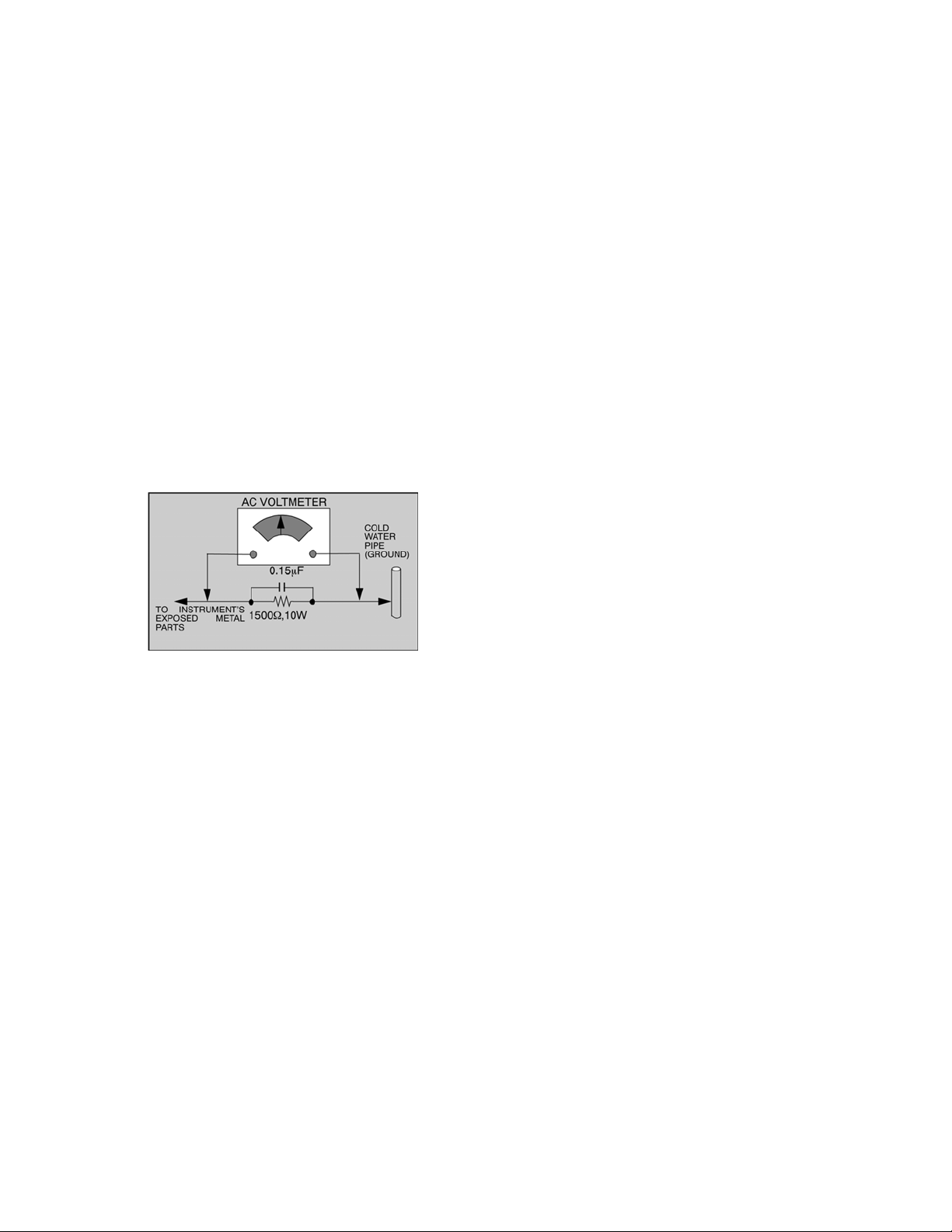
Figure 1. Hot check circuit
Leakage current hot check
1. Plug the AC cord directly into the AC outlet. Do not use
an isolation transformer for this check.
2. Connect a 1.5k, 10 watts resistor, in parallel with a
0.15F capacitors, between each exposed metallic part
on the set and a good earth ground such as a water
pipe, as shown in Figure 1.
3. Use an AC voltmeter, with 1000 ohms/volt or more
sensitivity, to measure the potential across the resistor.
4. Check each exposed metallic part, and measure the
voltage at each point.
5. Reverse the AC plug in the AC outlet and repeat each of
the above measurements.
6. The potential at any point should not exceed 0.75 volts
RMS. A leakage current tester (Simpson Model 229 or
equivalent) may be used to make the hot checks,
leakage current must not exceed 0.5 milliamp. In case a
measurement is outside of the limits specified, there is
a possibility of a shock hazard, and the equipment
should be repaired and rechecked before it is returned
to the customer.
2 Warning
2.1. Prevention of Electro Static
Discharge (ESD) to
Electrostatically Sensitive (ES)
Devices
Some semiconductor (solid state) devices can be damaged
easily by static electricity. Such components commonly are
called Electrostatically Sensitive (ES) Devices. Examples of
typical ES devices are integrated circuits and some fieldeffect transistors and semiconductor "chip" components.
The following techniques should be used to help reduce the
incidence of component damage caused by electro static
discharge (ESD).
1. Immediately before handling any semiconductor
component or semiconductor-equipped assembly, drain off
any ESD on your body by touching a known earth ground.
Alternatively, obtain and wear a commercially available
discharging ESD wrist strap, which should be removed for
potential shock reasons prior to applying power to the unit
under test.
2. After removing an electrical assembly equipped with ES
devices, place the assembly on a conductive surface such
as alminum foil, to prevent electrostatic charge buildup or
exposure of the assembly.
3. Use only a grounded-tip soldering iron to solder or unsolder
ES devices.
4. Use only an anti-static solder removal device. Some solder
removal devices not classified as "anti-static (ESD
protected)" can generate electrical charge sufficient to
damage ES devices.
5. Do not use freon-propelled chemicals. These can generate
electrical charges sufficient to damage ES devices.
6. Do not remove a replacement ES device from its protective
package until immediately before you are ready to install it.
(Most replacement ES devices are packaged with leads
electrically shorted together by conductive foam, alminum
foil or comparable conductive material).
7. Immediately before removing the protective material from
the leads of a replacement ES device, touch the protective
material to the chassis or circuit assembly into which the
device will be installed.
Caution
Be sure no power is applied to the chassis or circuit, and
observe all other safety precautions.
8. Minimize bodily motions when handling unpackaged
replacement ES devices. (Otherwise hamless motion such
as the brushing together of your clothes fabric or the lifting
of your foot from a carpeted floor can generate static
electricity (ESD) sufficient to damage an ES device).
3
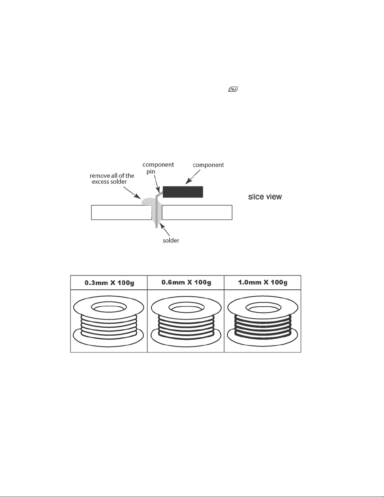
3 About lead free solder (PbF)
NOTE
Lead is listed as (Pb) in the periodic table of elements.
In the information below, Pb will refer to lead solder, and PbF will refer to Lead Free Solder.
The lead free solder used in our manufacturin g process and discussed below is (Sn+Ag+Cu).
That is Tin (Sn), Silver (Ag) and Copper (Cu) although other types are available.
This model uses Pb Free solder in it’s manufacture due to environmental conservation issues. For service and repair work, we’d
suggest the use of Pb free solder as well, although Pb solder may be used.
PCBs manufactured using lead free solder will have the “PbF” or a leaf symbol
CAUTION
• Pb free solder has a higher melting point than standard solder. Typically the melting point is 50 ~ 70 °F (30 ~ 40 °C) higher.
Please use a high temperature soldering iron and set it to 700 ± 20 °F (370 ± 10 °C).
• Pb free solder will tend to splash when heated too high (about 1100 °F or 600 °C).
If you must use Pb solder, please completely remove all of the Pb free solder on the pins or solder area before applying Pb
solder. If this is not practical, be sure to heat the Pb free solder until it melts, before applying Pb solder.
• After applying PbF solder to double layered boards, please check the component side for excess solder which may flow onto
the opposite side.
stamped on the back of PCB.
Suggested Pb free solder
There are several kinds of Pb free solder available for purchase. This product uses Sn+Ag+Cu (tin, silver, copper) solder.
However, Sn+Cu (tin, copper), Sn+Zn+Bi (tin, zinc, bismuth) solder can also be used.
4
4 Receiver feature table
FEATURE / MODEL TC-26LX60 TC-32LX60
LCD TYPE IPS (WXG A)
LCD PANEL MAKER LG
CHASSIS LH58
SYSTEM ATSC
TUNING FST
STEREO MTS/SAP
CATV USA CATV 181CH
POWER SUPPLY AC120, 60HZ
AV-IN 3 (RCA)
S-VHS-IN 2
COMPONENT VIDEO-IN VIDEO 1 / AUDIO 1 (RCA)
AV-OUT 1 (RCA)
HDMI 2 (AUDIO 2 IS COMMON VIDEO 2)
DVI NONE
PC-INPUT NONE
HEAD PHONE X
OPT DIGITAL AUDIO X
PEAKS SYSTEM PEAKS LITE
GC SYSTEM MICRONAS VCTP
PROGRESSIVE X
3D Y/CCOMB FILTER X
AUDIO OUTPUT 10W + 10W
SPEAKER SYSTEM UNDER/1 WAY - SPEAKER
BASS/TREBLE X
BALANCE X
SURROUND X
AUDIO OUT PERFORMANCE FAO
SAFETY-STANDARD UL6500/CUL
STANDARD-ORGANIZATION E-STAR
EMC (EMISSION) FCC-B/BETS-7
MECHANICAL ISTA
ASPECT X
OFF TIMER X
AUTO SEARCH X
DEMOSTRATION MODE X
CLOSED CAPTION X
V-CHIP X
VESA COMPATIBLE
OSD LANGUAGE ENGLISH (US) / FRENCH / SPANISH
REMOTE CONTROLLER EUR7613ZG0
CEC OF HDMI CONNECTION DIGA
PEDESTAL SWIVEL ONLY (NO TILTED)
SD SLOT FOR DL BACK SIDE
Note:
Specifications are subject to change without notice or obligation.
5
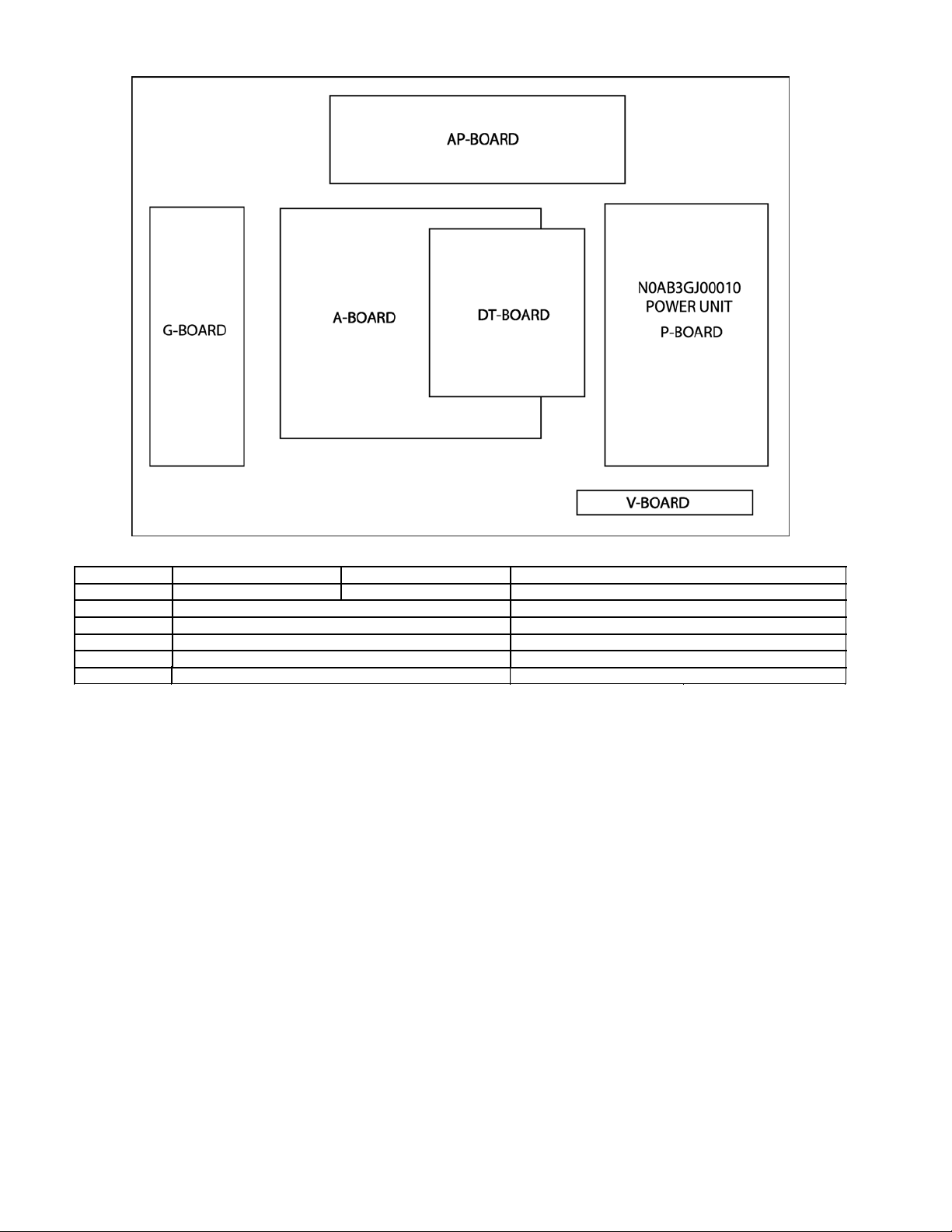
5 Chassis Board Layout
Board Layout
Board Name TC-26LX60 TC-32LX60 Function
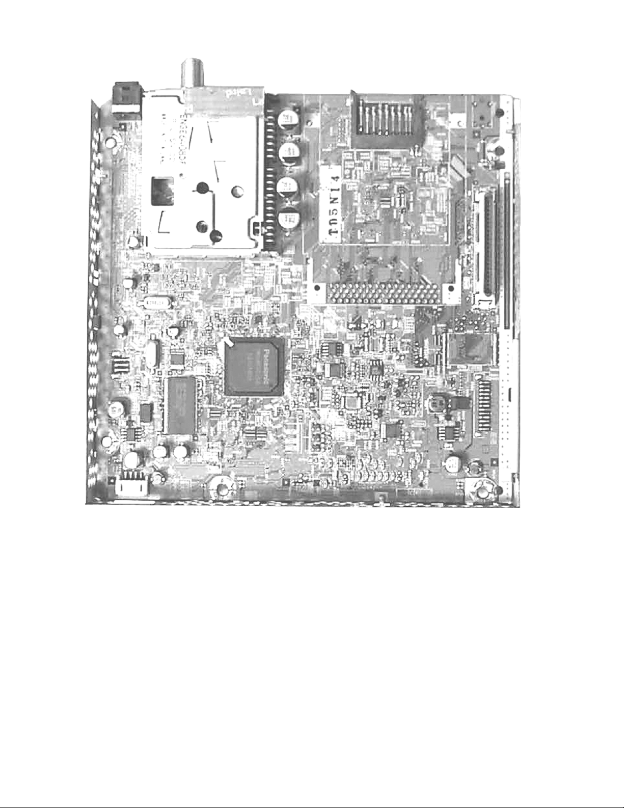
A-Board TZRXN010MZK TZRXN010MYK Main (AV Switch, Audio, MCU, Global Core, AV connector)
AP-Board TZRXN020MYK DC-DC
DT-Board TNAG169S Digital Tuner
G-Board TNPA3784S Front Terminal
V-Board TNPA3749ACS Remote Reciever, LED
P-Board N0AB3GJ00010 AC-DC
6
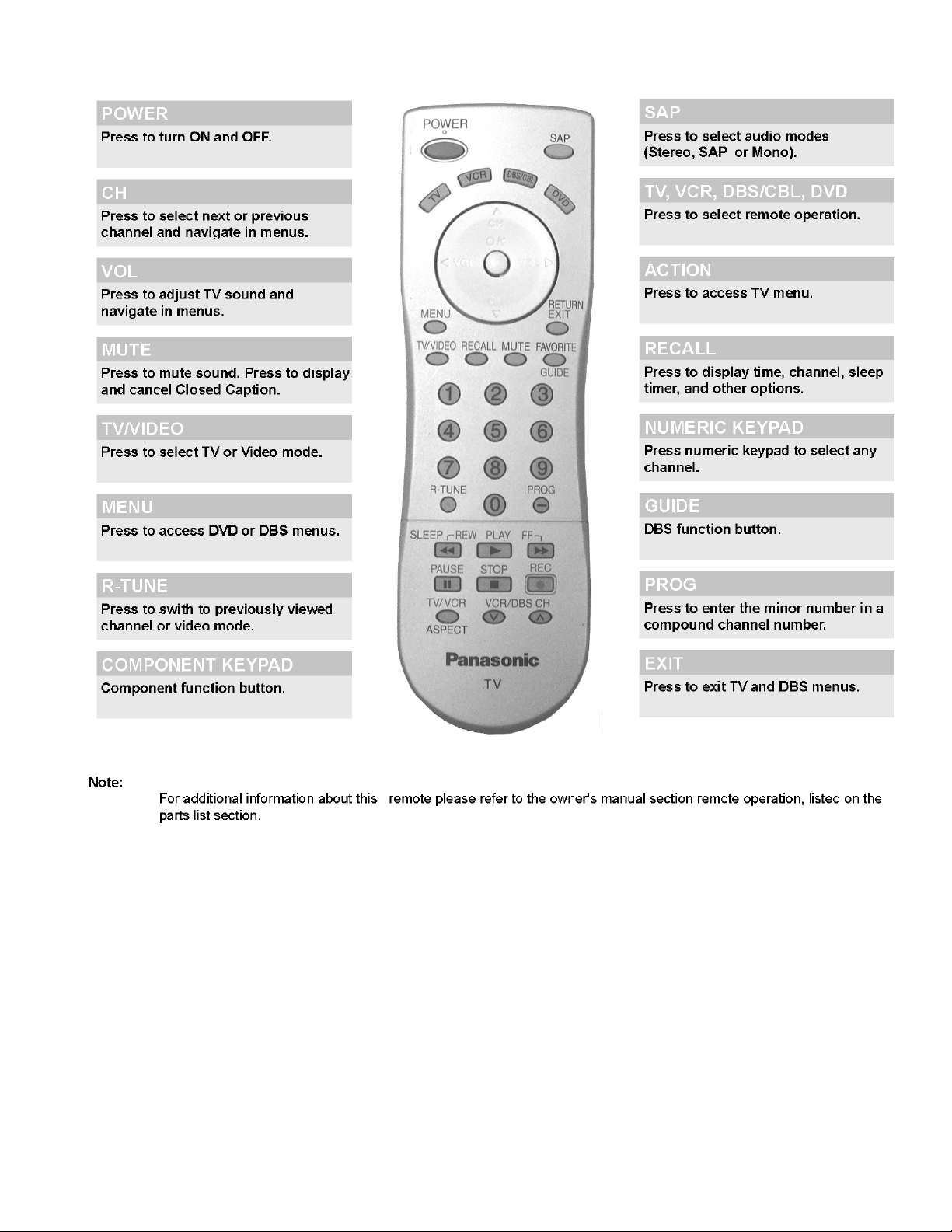
6 Location of controls (EUR7613ZG0)
7
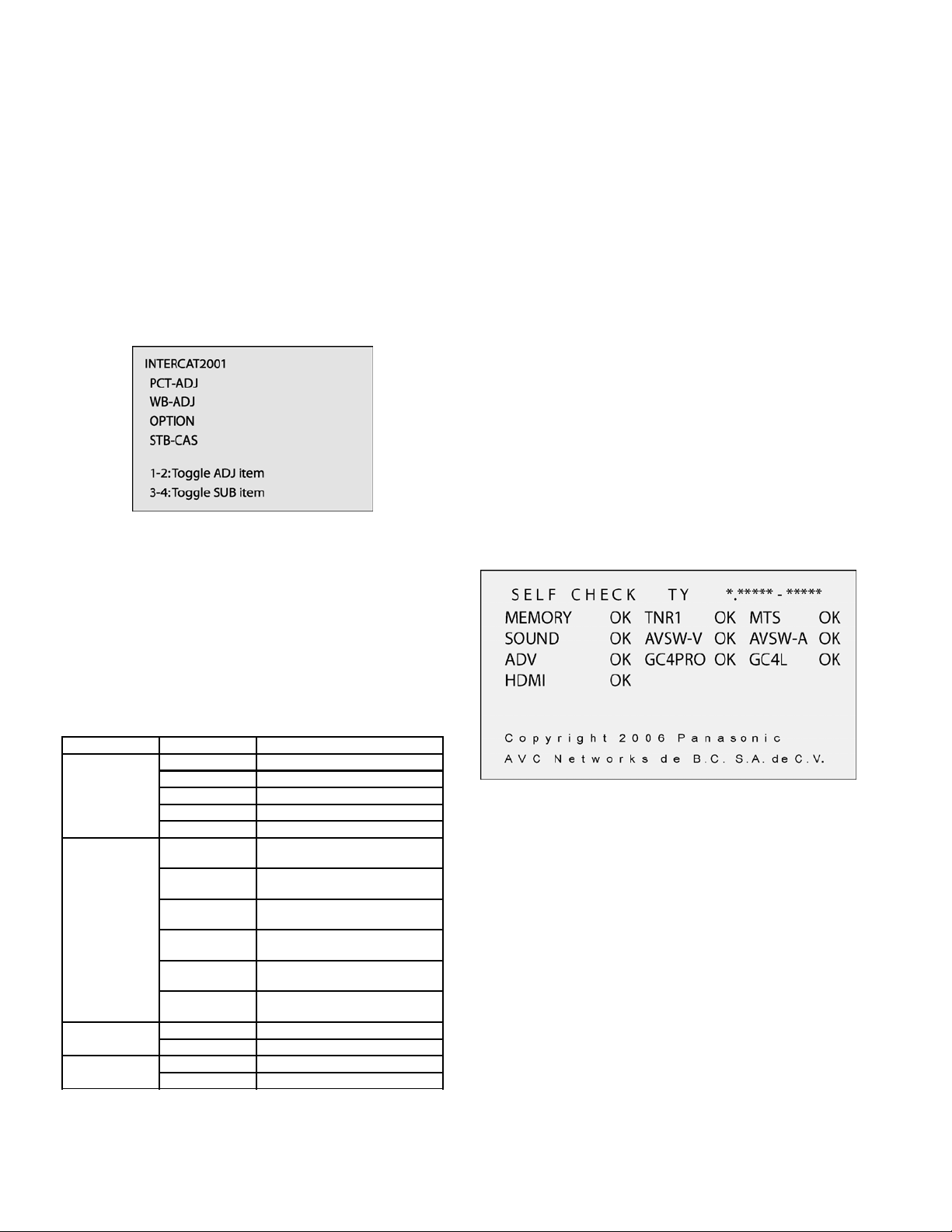
7 Service Mode
8 Troubleshooting Guide
7.1. How to enter into adjustment
mode
While pressing [VOLUME-] button of the main unit, press
[RECALL] button of the remote control transmitter three times
in a row (within 2 seconds).
7.2. Adjustment method.....Use the
remote control.
“1” button...Main items Selection in forward direction
“2” button...Main items Selection in reverse direction
“3” button...Sub items Selection in forward direction
“4” button...Sub items Selection in reverse direction
7.3. Cancellation
8.1. Self-check function
When phenomena like "the power fails from time to time" or
"the video/audio fails from time to time" can not be
confirmed at the time of servicing, the self-check function
can be used to confirm the occurrence and to limit the
scope for the defective circuits. Also, when "the power fails
from time to time", display on the screen can be used to
confirm the occurrence and to limit the scope for the
defective circuits.
Any programmed channels, channels caption data and
some other user defined settings will be erased and return
to factory setting.
8.2. How to access
Access
Produce TV reception screen and, while pressing
[VOLUME -] button on the main unit, press [SLEEP] button
on the remote controller unit simultaneously.
Exit
Press the POWER button twice (off/on) to return to the
normal screen.
8.3. Screen Display
Switch off the power with the [POWER] button on the main unit
or the [POWER] button on the remote control.
7.4. Contents of adjustment mode
• Value is shown as a hexadecimal number.
• Preset value differs depending on models.
• After entering the adjustment mode, take note of the value
in each item before starting adjustment.
Main Item Sub Item Remarks
PCT-ADJ COLOR Sub color
R-Y-A R-Y recovery axis (R-Y)
R-Y-G B-Y Gain (B-Y)
BACK-L Sub backlight
TINT Tint Adjustment
WB-ADT B-CENT Adjustment of Blue gain by test
G-CENT Adjustment of Green gain by test
R-CENT Adjustment of Red gain by test
B-GAIN Adjustment of Blue gain by test
G-GAIN Adjustment of Green gain by test
R-GAIN Adjustment of Red gain by test
OPTION OPTDD White 100% (Not ADJ)
BOOT Red 100% (Not ADJ)
STB-CAS
pattern (50% white)
pattern (50% white)
pattern (50% white)
pattern (100% white)
pattern (100% white)
pattern (100% white)
8
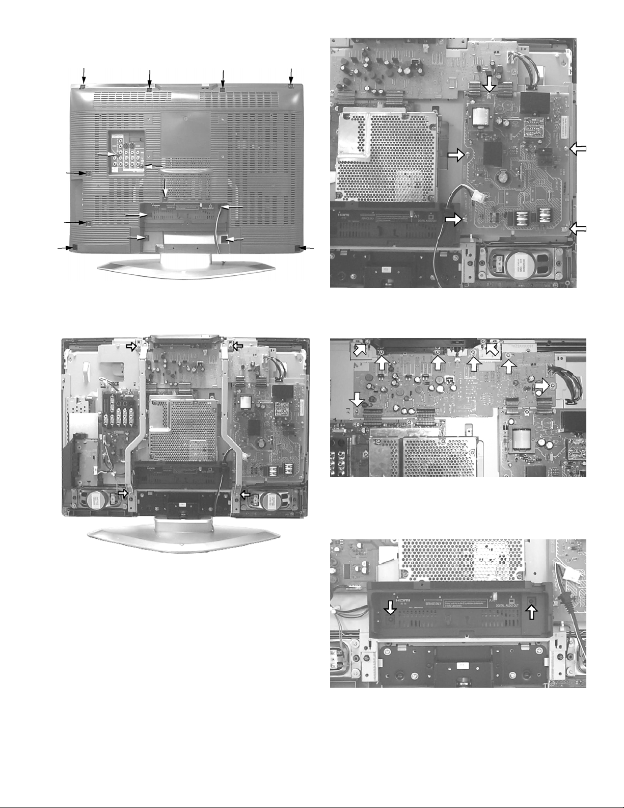
9 Disassembly Instructions
Back cover removal (screw location)
P-Board Disassembly
1. Remove all the screw from the back cover indicated with
arrows.
Without the back cover
1. First remove the two screws from each bracket one
located on top and one on the bottom.
1. To remove the P-Board remove the screws indicated on
the figure above by arrows.
AP-Board Disassembly
1. To remove the AP-Board first lift the four connectors
then remove the screws indicated on the figure above
by arrows.
Bracket Disassembly
1. To remove the bracket shown above remove the screws
indicated on the figure above by arrow.
9
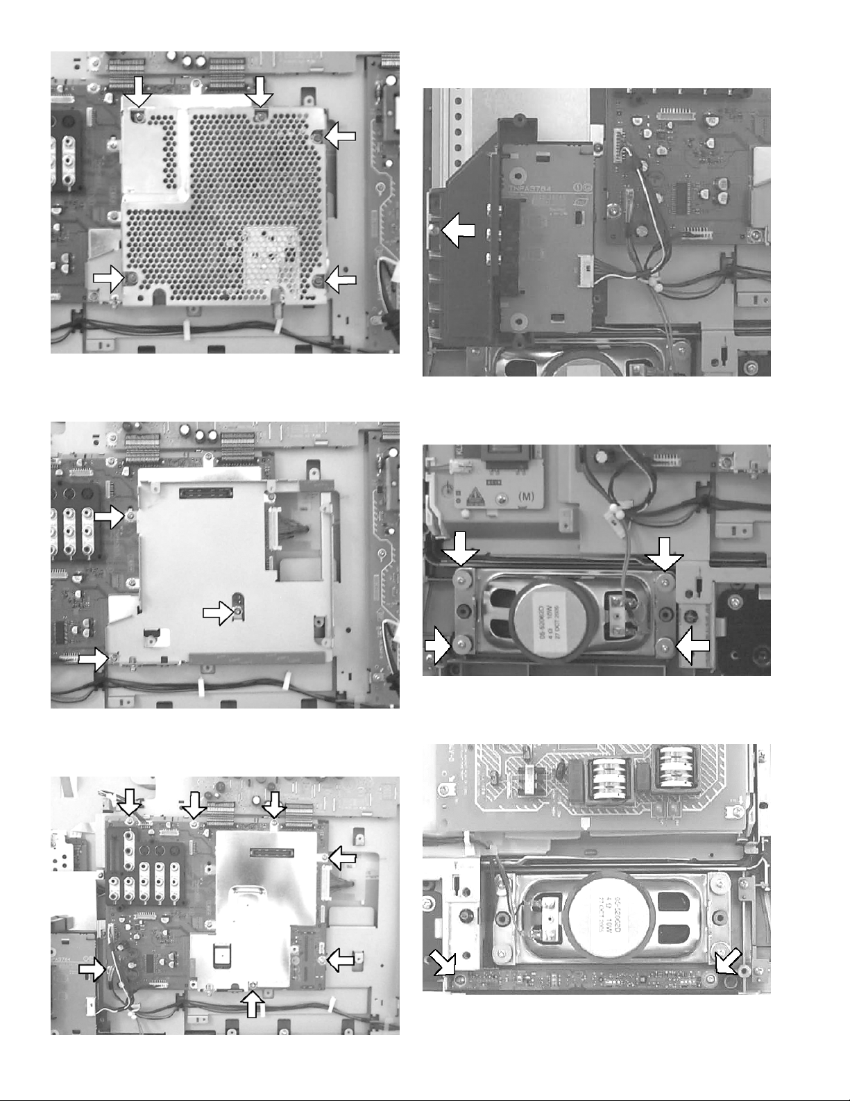
DT-Board Disassembly
1. To remove the DT-Board shown above remove the
screws indicated on the figure by arrows.
DT-Board Bracket Disassembly
1. To remove the A-Board bracket shown above remove
the screws indicated on the figure above by arrows.
G-Board Disassembly
1. To remove the G-Board shown above remove the screw
indicated on the figure by arrow.
Speaker Disassembly
1. To remove the DT-Board bracket shown above remove
the screws indicated on the figure above by arrows.
A-Board Disassembly
1. To remove the speaker remove the screws indicated on
the figure by arrows, each speaker is located on sides.
V-Board Disassembly
1. To remove the V-Board remove the screws indicated on
the figure by arrows.
10
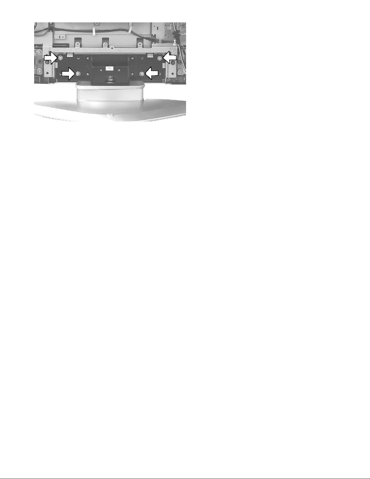
Removing the pedestal
1. Lay down the unit so that the rear cover faces upward.
2. Remove the 4 screws.
3. Then remove the pedestal.
11
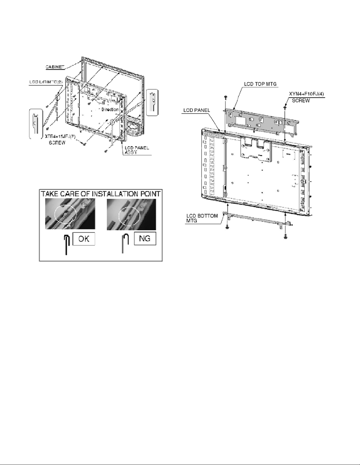
9.1. Removing the LCD panel
assembly and LCD L/R MTG
1. Remove the 4 screws.
2. Remove the LCD panel ass’y and LCD L/R MTG.
9.2. Removing the LCD panel and
LCD T/B MTG
1. Remove the 4 screws.
2. Remove the LCD panel and LCD T/B MTG.
12
10 Measurements and
Adjustments
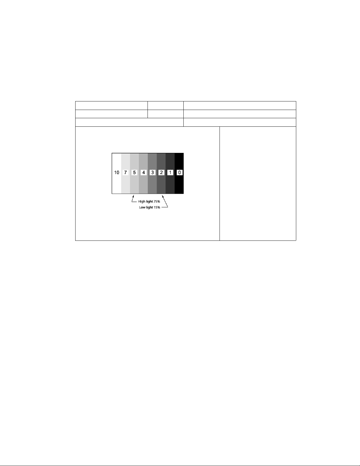
10.1. White Balance Adjustment
!"#$%&'("$)*+'( ,-""(.$)$- /0(.121.+$1-"
3('-$().-"$%-44(%
5%-.(6&%(
78 9004:)+);<1$()0+$$(%")-"()<-&%)=(2-%()+6>&#$'("$8
?8 51.$&%()'-6()$-)@1A168
B8 C+.DE1F<$)$-)GBH8
I8 9!))51.$&%()$-)-228
J8 9004:)+).-4-%)=+%)0+$$(%"8
U1)41F<$)V"-%'+4WX)YZ?RJ[JN)\Z?TB[J]
U1)41F<$)V;+%'WX)YZB7I[JN)\ZB?I[J]
E-;)41F<$)V"-%'+4WX)YZ?RJ[JN)\Z?TB[J]
U1)41F<$)V;+%'WX)YZB7I[JN)\ZB?I[J]
K8 /($)$<().-4-%)$-)'1"1'&'8
L8 M<(")=4&()1#)4(##))4&'1"+".()$<+")%(6)-%)F%(("N)COP+1")=:)6(2+&4$)1#)QQ8)
R8 96>&#$)S+.#)3OP+1")+"6)POP+1")$-)-=$+1")#0(.121.+$1-"8
T8 /($)PO,("$)+#)%(2(%(".(8
7H8 96>&#$)S+.#)3O,("$)+"6)CO,("$)$-)-=$+1")#0(.121.+$1-"8
778 3(0(+$)0%-.(6&%()$-)-=$+1").--61"+$(#8
13
11 Boards Assemblies
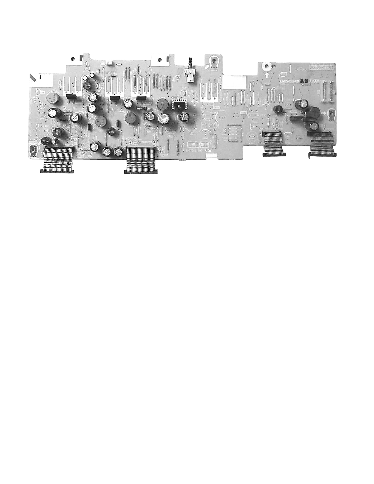
11.1. AP-Board
14
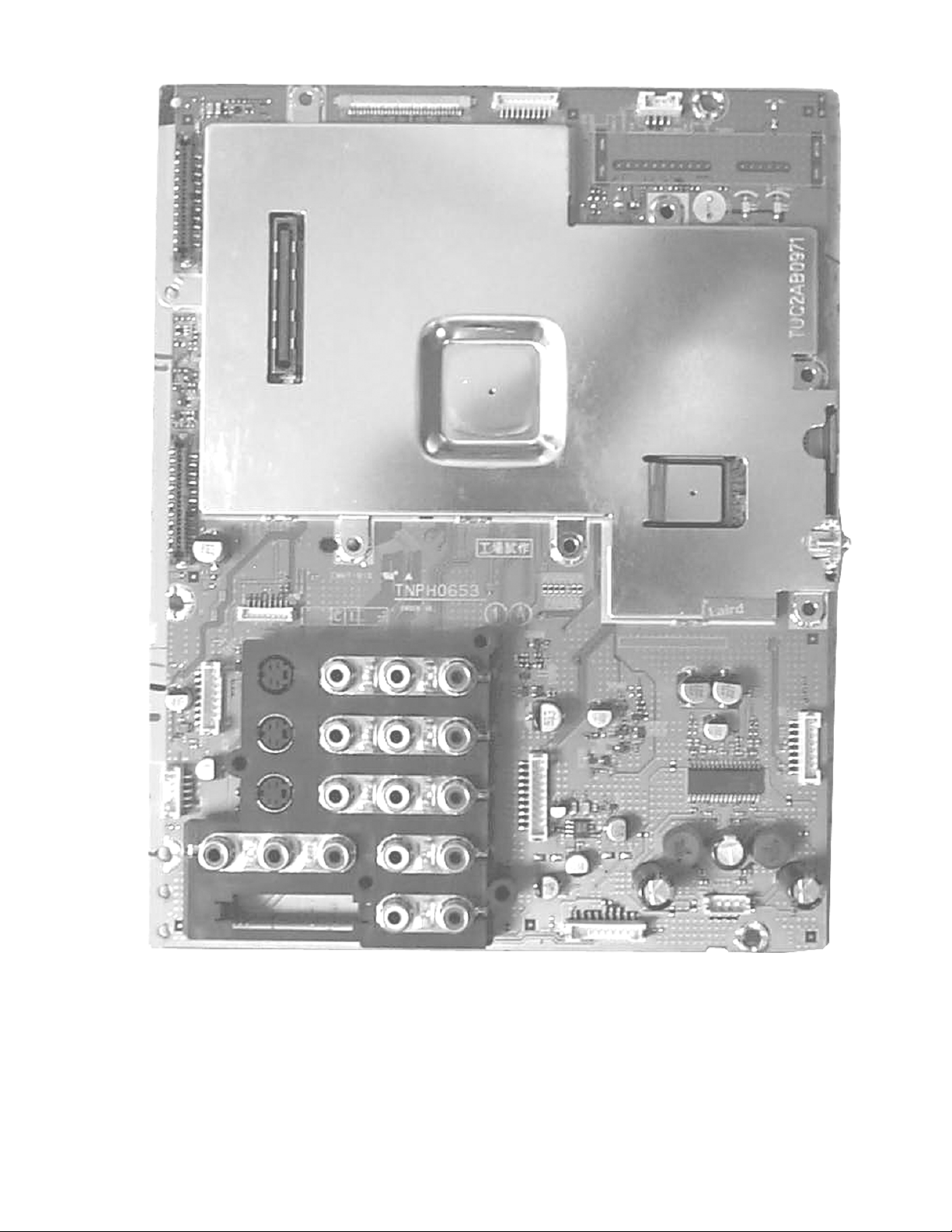
11.2. A-Board
15
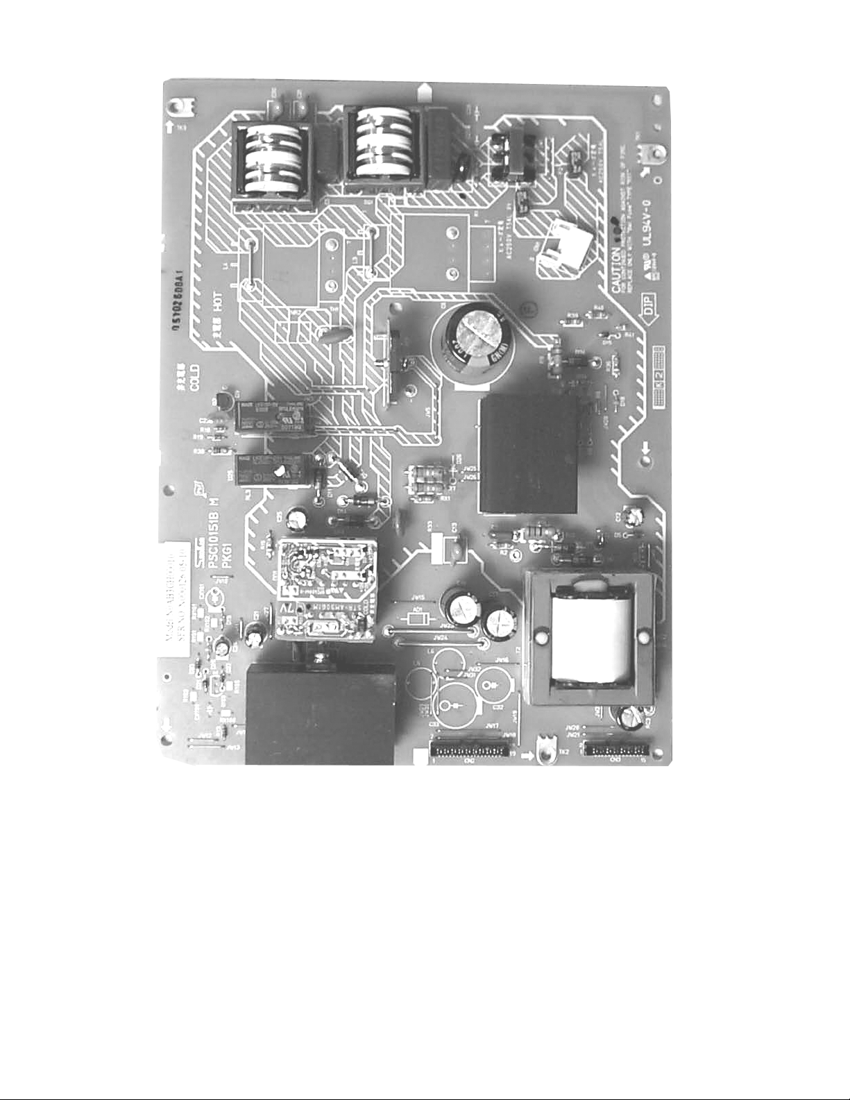
11.3. P-Board
16
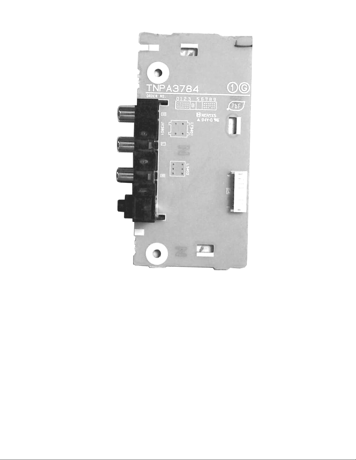
11.4. G-Board
17
11.5. DT-Board
18
 Loading...