

Page 1
Technical Guide
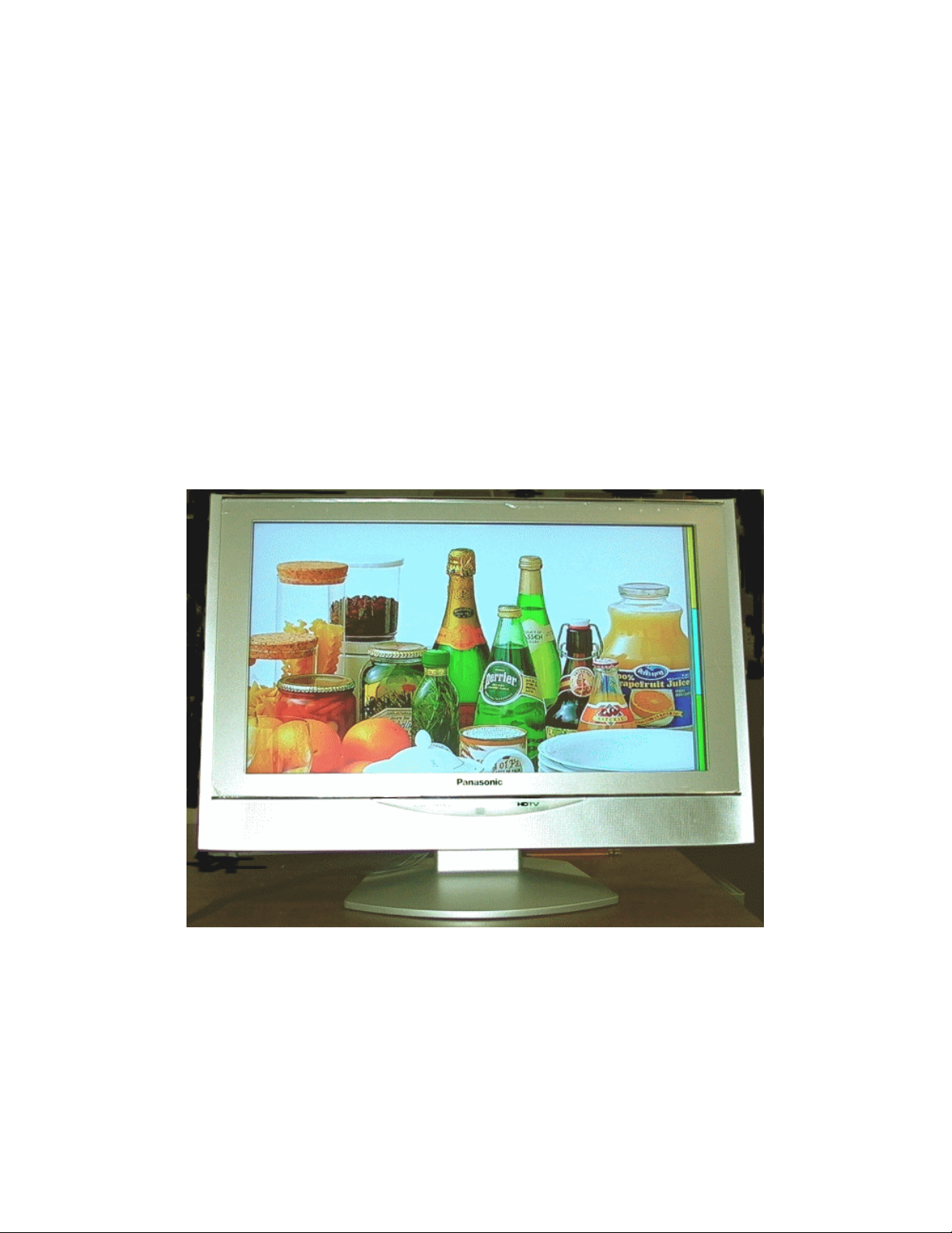
TC-22LH1
LCD Television
Technology, Troubleshooting, &
Adjustments
Panasonic Services Company
National Training Center
Page 2

Produced by
Gerald Gaimo &
Jean Magloire
Panasonic Services Company
National Training Department
Secaucus, NJ
Warning
This service information is designed for experienced repair technicians only and is not designed for use by
the general public. It does not contain warnings or cautions to advise non-technical individuals of potential
dangers in attempting to service a product. Products powered by electricity should be serviced or repaired
only by experienced professional technicians. Any attempt to service or repair the product or products
dealt with in this service information by anyone else could result in serious injury or death.
Table Of Contents
2
Page 3

Introduction ........................................................................................................ 5
Chapter 1 Technology Explanation .................................................................. 7
1.1 Properties of Liquid Crystals..................................................................................7
1.2 LCD Basic Reflective Assembly.............................................................................8
1.3 Backlighting vs. Reflective.....................................................................................8
1.4 Color......................................................................................................................9
1.5 LCD Addressing Technology...............................................................................10
1.6 Backlighting .........................................................................................................11
1.7 Inverter Power Supply ......................................................................................... 11
1.8 High Voltage Power Supply.................................................................................12
1.9 Test and Measurement........................................................................................13
1.10 Features ............................................................................................................14
Chapter 2 Circuit Descriptions........................................................................ 16
Block Diagram Overview ...........................................................................................18
Chapter 3 Video Circuit Explanations ............................................................ 20
Video Signal Block Diagram......................................................................................20
NTSC Video Signal Path ...........................................................................................22
ATSC Video Signal Path............................................................................................23
HDMI Signal Path......................................................................................................24
Picture Processing.....................................................................................................25
Resizing The Screen ................................................................................................. 27
Chapter 4 Audio Circuit Explanations............................................................ 28
Audio Signal Block Diagram......................................................................................28
Multiplexed Television Sound (MTS)........................................................................29
Surround Sound Processing......................................................................................31
Power Supply Section................................................................................................32
Chapter 5 Unit Disassembly ...................................................................34
Rear Cover Removal.................................................................................................34
AP Board Removal....................................................................................................35
DV Board Removal.................................................................................................... 36
DG Board Removal....................................................................................................36
B1 Board Removal.....................................................................................................37
H Board Removal ......................................................................................................37
Speaker Removal......................................................................................................38
K Board (Button Board) Removal ..............................................................................38
V Board (remote sensor) Removal ............................................................................39
LCD Panel Removal.................................................................................................. 39
Chapter 6 Self Check and Adjustment ........................................................... 41
Self Check.................................................................................................................41
Service mode Adjustment..........................................................................................42
Main Adjustment SUB Adjustment.............................................................................43
3
Page 4

SUB Adjustment ........................................................................................................44
LCD Pixel Specifications............................................................................................45
4
Page 5

Introduction
The information provided in this document is designed to give the technician a brief
overview of the LCD display technology. It is also intended to help the technician
diagnose and identify the defective printed circuit board, efficiently. This guide covers
the Panasonic TC-22LH1 LCD television. Troubleshooting flow charts, signal path
diagrams, and connector information are included to provide enough details, so the
technician could accurately determine which of the boards contains the source of the
problem. Alignment and adjustment procedures are also included in this document to
complement the information available in the service manual.
5
Page 6

6
Page 7
Chapter 1 Technology Explanation
1.1 Properties of Liquid Crystals
Liquid Crystals exist in an unusual state that is somewhat like a liquid and a solid. The
molecules in this state tend to maintain their orientation like molecules in a solid but also
move around to a different position like a liquid. There are several distinct phases of
liquid crystals, dependent upon how they are used.
A twisted nematic (TN) LC display consists of two polarizing filters, two pieces of glass,
some form of switching element or electrode, which is connected to a power source as
depicted in Figure 1. An applied voltage is used to untwist one pixel.
Figure 1
7
Page 8
1.2 LCD Basic Reflective Assembly
Figure 2A represents a basic LCD assembly, which is comprised of the following: A
mirror (A), which is located on the rear of the assembly, provides for the reflection of
light. A piece of glass (B) layered with a polarizing film is coated on the bottom side of
the mirror, and a common electrode plane (C) made of indium-tin oxide is placed top. A
common electrode plane covers the entire area of the LCD. Above that is the layer of a
liquid crystal substance (D). This is followed by another piece of glass (E) with an
electrode in the shape of a rectangle etched on the bottom side. Another polarizing film
(F), which is layered on top, is right angle orientated to layer (B). A power source is
connected to the electrode. When no current is supplied to the electrode (E), light
entering through the front of the LCD will be reflected off the mirror and bounce right
back out. When current produced by the power source is applied to the electrode (E),
the liquid crystals between the common-plane electrode and the electrode shaped like a
rectangle untwist and block the light in that area from passing through. The rectangle
ithin LCD appears as a black area. w
Figure 2a
1.3 Backlighting vs. Reflective
Most computer displays are lit with built-in fluorescent tubes above, beside and
sometimes behind the LCD. A white diffusion panel behind the LCD redirects and
scatters the light evenly to ensure a uniform display on its way through filters, liquid
crystal layers and the electrode layers. By adding to the layer that contains the single
electrode, more enhanced displays can be designed.
Figure 2b
8
Page 9
1.4 Color
An LCD that can show colors must have three sub-pixels (red, green and blue color
filters to create each color pixel. These sub pixels are created by applying color filters
that allow only certain wavelengths to pass through them while absorbing the rest. With
a combination of red, blue and green sub pixels of various intensities; a pixel can be
made to appear in many different colors
Through the control and variation of the applied voltage, the intensity of each sub pixel
can range over 256 shades. Combining the sub pixels produces a palette of 16.8
million colors (256 shades of red x 256 shades of green x 256 shades of blue), as
shown below. These color displays take an enormous number of transistors. For
example, a typical laptop computer supports resolutions up to 1,024x768. If we multiply
1,024 columns by 768 rows by 3 sub pixels, we get 2,359,296 transistors etched onto
the glass! If there is a problem with any of these transistors, it creates a "bad pixel" on
the display. Most active matrix displays have a few bad pixels scattered across the
screen. Figure 3 can give you an idea of the RGB sub pixels within each color pixel.
Figure 3
9
Page 10
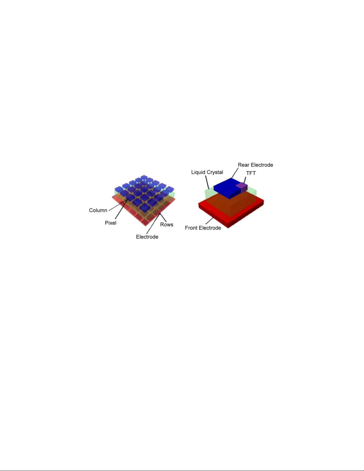
1.5 LCD Addressing Technology
An Active Matrix LCD is a common type of LCD used in laptops, cameras, LCD
projection panels and LCD TVs that depend upon thin film transistors (TFT). TFTs are
small switching transistors and capacitors arranged in a matrix on a glass substrate as
referenced in figure 4. In order to address a particular pixel the proper row must be
switched on, and then a charge is sent down the correct column. Since all of the other
rows that the column intersects are turned off, only the capacitor at the designated pixel
gets a charge. The capacitor is able to hold the charge until the next refresh cycle.
Pixels within the display are addressed by applying current to a gate line, which
switches the TFT on and allows charge from the source line to flow on to the rear
electrode. This sets up a voltage across the pixel and turns it on.
Figure 4
For example, a high definition LCD TV model such as the TC-22LH1 supports
resolutions up to 1,280x720. If we multiply 1,280 columns by 720 rows by 3 sub pixels,
we get 2,764,800 transistors etched onto the glass! If there is a problem with any of
these transistors, it creates a "bad pixel" on the display. Most active matrix displays
have a few bad pixels scattered across the screen.
10
Page 11
1.6 Backlighting
Backlighting Brightness for Panasonic’s line of LCD TVs is accomplished through the
use of Cold Cathode Fluorescent tubes (CCFT), which is currently the light source of
choice, by a number of leading manufacturers.
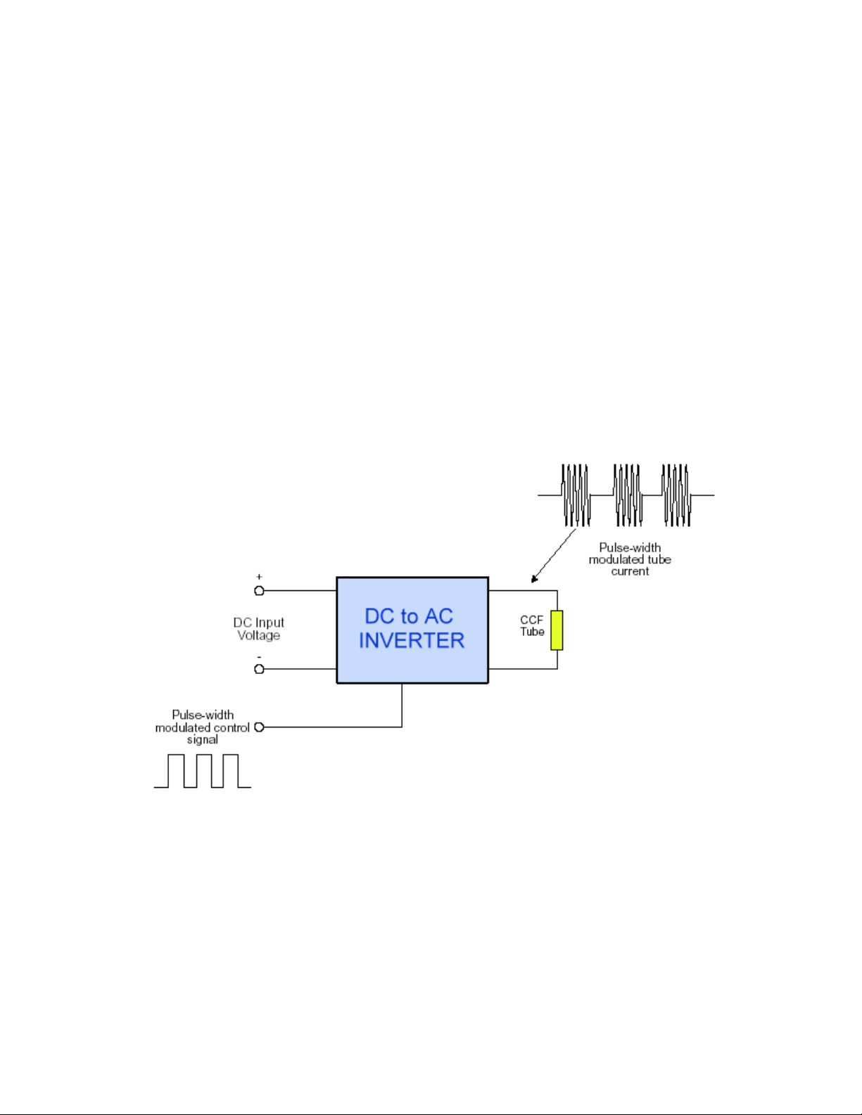
1.7 Inverter Power Supply
Pulse width modulation is a very straightforward method for controlling the brightness of
the CCF tube(s). The inverter is turned on and off (using the input or an enable/disable
line) from the Microprocessor Unit (MPU) to control the brightness. The “on” duty cycle
is lengthened to increase the brightness and reduced to decrease the brightness. One
of the major advantages of pulse width modulation is the tube is always fully “on” or fully
“off” and full starting voltage is always applied to the tube(s) (assuming nominal input
voltage. Figure 5 is a simplified diagram of a pulse width modulated DC to AC inverter.
Figure 5
11
Page 12
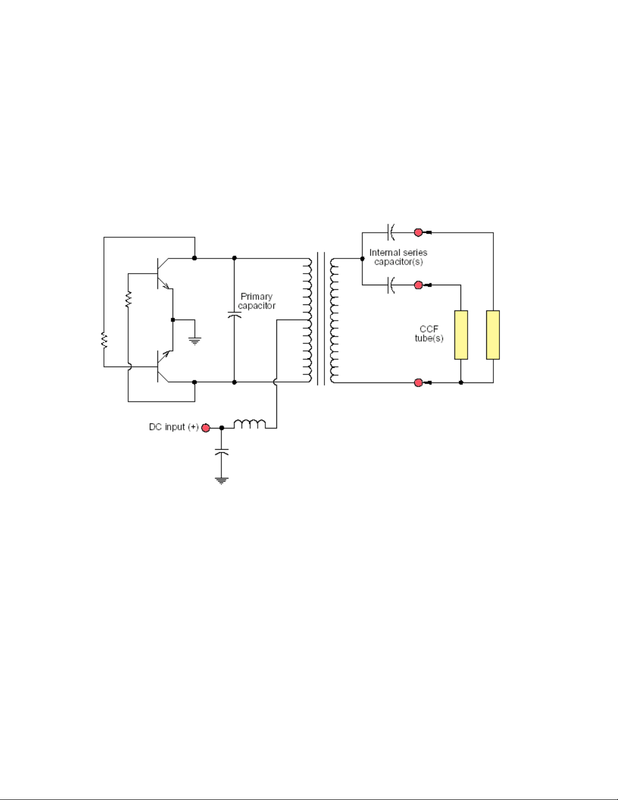
1.8 High Voltage Power Supply
A CCF tube needs high voltage. The starting voltage is generally over 1,000 volts and
the operating voltage is generally between 200 and 500 volts rms.
Most CCFT DC to AC inverters are tuned switchers designed to produce a specific
voltage, frequency and output current when a designated tube is connected to the
output. The classic current-fed two-transistor inverter has a tuned resonating output,
tuned resonating input and inductive dc input which provides for good power transfer
and high operating efficiency.
Figure 6
T
he type of circuit depicted in Figure 6 inherently produces a pure sine-wave output, but
the voltage and current waveforms are both distorted when they are applied to a CCF
tube, which is a highly nonlinear device. The transition from the starting voltage to the
operating voltage in this circuit is implemented by a small internal series output
capacitor, which serves as the ballast, providing impedance, and allowing prope
current after the tube has been ignited.
12
r tube
Page 13
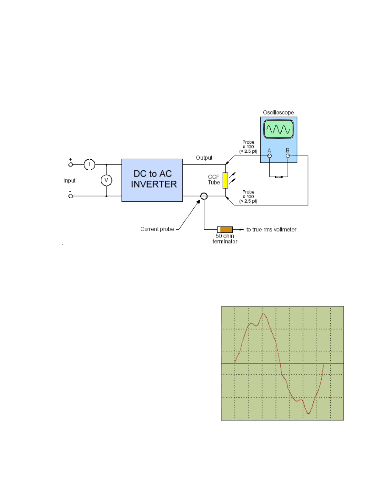
1.9 Test and Measurement
This is a basic test setup for measuring the output voltages of the inverter circuit. The
output voltage to the tube can be measured with a dual-channel oscilloscope and two
low-capacitance (< 2.5 pf) scope probes. The oscilloscope should be connected
differentially, with the probe grounds connected and floating as depicted in the diagram.
Figure 7 indicates how an oscilloscope can be used for achieving these measurements.
Figure 7
Channel A should be added to the inverse of channel B to produce the complete
waveform on the oscilloscope.
O
utput waveform
Figure 8 is what th
should look like as viewed in the above test
arrangement.
e typical output current waveform
Figure 8
13
Page 14

1.10 Features
ACTIVE SYSTEM CONTROL
Working in tandem with active light control, this technology adjusts the video signal
according to the image contrast, adding greater brightness to bright scenes and more
depth to darker ones, giving you more vivid images and a more powerful viewing
experience.
SUPER DYNAMIC SHARPNESS CONTROL
By analyzing the entire image, minimizing noise in areas of low detail (such as a
cloudless sky), and enhancing areas with greater detail, this circuitry provides a natural,
lifelike picture with outstanding detail.
16:9 ASPECT RATIO
These wide screen TVs have a width-to-height ratio similar to movie theater screens,
providing one with cinema-style entertainment right in your own home. Thus enabling
full-screen viewing of high-definition broadcasts and DVD videos, in a 16:9 format.
PROGRESSIVE SCAN DOUBLER
Displays a full frame of video in 1/60th of a second by de-interlacing the incoming video
signal and progressively scanning the image. This feature helps to reduce the horizontal
scan lines that are often visible in ordinary television images.
3D Y/C DIGITAL COMB FILTER
The 3D Y/C digital comb filter performs field-by-field comparisons of the television
image to accurately separate the color from the black-and-white information. The filter
works to minimize both horizontally and vertically hanging dots, as well as dot crawl.
Component Video Input Jacks
Each of the two components video input jacks consist of a luminance signal and two
separate chrominance signals. These three combined inputs provide video images with
a superior resolution and color accuracy. Panasonic televisions with these component
video inputs can accept either progressive or interlaced signals from a variety of
sources, including DVD players and DTV set-top boxes.
S Video And Composite Input Jacks
Two S video input and Composite connections are available on this model The S video
input jacks consist of a luminance signal and chrominance signal each. These in
addition to the Composite Video input jack provide video signals that are selected via
the A/V switch.
HDMI-DVI Interface
The unit is equipped with a High Definition Multimedia Interface (HDMI), which is
considered to be the first all digital consumer electronics A/V interface that supports
both Digital Video and Audio. DVI currently does not support audio.
14
Page 15

TC-22LH1 LCD TV Model Specification
15
Page 16

Chapter 2 Circuit Descriptions
TC-22LH1 Board Descriptions
Board Name Function
AP-Board Power
B1-Board Tuner
DG-Board GC2, PCN, MICOM, EEPROM
DV-Board HDMI, DVI Interface
H - Board DC – IN, Audio Switch, AV Switch
K - Board Switches
V - Board Remote Sensor, LED
Figure 9
Figure 9 represents the circuit board layout followed by a brief description of the
functions of each board.
16
Page 17

AP Board
The AP board contains the Main DC power supply, which provides the starting voltage
to the backlight inverter power supply, which is part of the LCD Panel assembly. The
30V tuner voltage is also derived on this board.
B1 Board
The B1 board contains a single tuner, which provides a Composite video input to the AV
switch, which is located on the H board.
DG Board
This board is responsible for processing all incoming video signals from the H board
and the B1 tuner board. It also converts the input signals into the LCD format required
to drive the LCD panel. Pixel conversion, White Balance, Aspect Ratio, I/P conversion,
Screen resizing and panel control all takes place on this board.
V Board
The V board houses the remote sensor and the power on / standby LED.
H Board
The H board serves as the motherboard and contains the 15 VDC Input, the MTS, the
Audio Switches / Amplifiers and the AV Switch.
K Board
The K board contains the Front Panel switches and interconnects with the AP board.
DV Board
The DV board contains the High Definition Multimedia Interface (HDMI), which handles
the digital video input in addition to digital audio.
17
Page 18

Block Diagram Overview
Figure 10
igure 10 contains a Block Layout overview of the LCD TV. The following is a
F
description of each of the boards that are depicted in the block.
Board
H
The H boa
audio and video input signals, an audio control circuit which handles all available soun
adjustments and stereo sound separation (MTS decoder), a DC-to-DC converter and
power input to the AP board.
V Switch
A
The AV Swit
Component, S -Video inputs and the output of the Tuner (B1) board. The Audio is
switched through this IC to a Control Amplifier, which drives the speakers. The sele
video signals are output to the DG Board.
rd is comprised of the following, an AV switch responsible for switching all
ch IC, located on the H board, handles the selection of the Composite,
cted
d
18
Page 19

Main CPU
The Main CPU, located on the DG board, handles all analog operations of the unit via
the IIC bus lines. It provides the OSD vertical and horizontal sync to the Pixel converter.
The OSD RGB signals are buffered and output to the Global Core IC, IC4004, for
mixing with the picture information. It also provides the data for resizing the LCD screen.
It monitors additionally the safety circuits responsible for shutting down the unit in the
event of a component failure.
Audio Control Circuitry
The audio control circuitry handles all available sound adjustments and stereo sound
separation (MTS decoder).
DG Board
The main function of this board is to process the incoming video signals and format
them in order to provide the necessary data for addressing the active matrix LCD
display.
HDMI-DVI Interface
The DV Board contains the HDMI-DVI Interface. HDMI (High Definition Multimedia
interface is considered to be the first all digital consumer electronics A/V interface that
supports several uncompressed standard, enhanced and high definition video format as
well as existing multi-channel audio format. DVI currently does not support audio.
Note: If the external device has DVI output only, use a DVI to HDMI adaptor cable to
connect to the HDMI jack on the TV. Also, connect the Audio Out signal from
the external device (set top box or DVD player) to the Audio In jacks. An HDMI
DVI conversion cable (TY-SCH03DH) is available at the Panasonic parts
department.
19
Page 20

Chapter 3 Video Circuit Explanations
Video Signal Block Diagram
Figure 11
Video Inputs
Figure 11 is a basic depiction of the video signal flow from the initial input switching
stage to video processing and output.
The TC22LH1 incorporates a single NTSC tuner that provides a composite video and a
multiplex audio output. The video output of the tuner is connected to the Audio /Video
(AV) input switch IC located on the H board. The unit also contains two S-Video
composite inputs; two component inputs and an HDMI (High Definition Multimedia
Interface) input connector that also connect to the A/V switch IC. The A/V switch IC
selects one of 6 video inputs. Selection is controlled by the MPU located on the DG
board via the I
2
C Bus control lines (SDA & SCL).
20
Page 21

Unlike other Panasonic television receivers IC4010 is not used for processing Picturein-Picture. The unit does not have a PIP function. IC4010, the sub global core IC is
specifically used to perform interlace to progressive (I/P) conversion for the 480i video
format. Since the components inputs are already Y/C separated, they are converted to
digital and totally bypass the comb filter section of the IC. The 480p and 1080i ATSC
Video signals simply pass through the IC and output to the main global core IC, IC4004.
IC4004 processes all NTSC inputs including the tuner output. Its output is a selection
between its NTSC input and the component output of IC4010. This process will be
discussed in the video signal flow section of this technical guide.
The Pixel Converter IC6000, which is located on the DG board, is responsible for
handling the White Balance and Picture Control processes. Interlace to progressive
conversion of all inputs is accomplished within this IC.
The LCD panel is designed to display a resolution of 1280X720 pixels.
Resizing the image to meet the specification of the LCD Screen is accomplished by
IC6100 located on the DG board. The Aspect Zoom and the LCD Frequency Drive logic
reside on this IC.
IC6400 is a Low Voltage Differential Signaling circuit (LVDS) designed to provide proper
drive and impedance matching when transmitting either data or signaling from one
board’s processor to another.
21
Page 22

NTSC Video Signal Path
Figure 12
The TC-22LH1 incorporates a single NTSC tuner located, on the B1 board for viewing
television broadcasts as depicted in Figure 12. It is also equipped with two auxiliary
NTSC Video inputs and two NTSC S-Video inputs. These video and audio signals
provide input to the AV switch IC3004 located on the H board. The video output signals
enter the DG board via connector H4/DG1.
Due to the limited capacity of IC3004, switching between the composite video inputs
and the luminance of the S-video inputs is accomplished by IC3000. The video outputs
of IC3004 are buffered and output to the DG board via the connector H4/DG1.
22
Page 23

ATSC Video Signal Path
Figure 13
The component video signals Y, Pb and Pr are input to the AV switch IC3004 as
depicted in Figure 13. The selected component video signal is buffered and provided to
the DG board via connector H4 pins 31,29 and 27.
If the selected input is HDMI, the Pr signal is output on pin 33 of the connector H4.
23
Page 24

HDMI Signal Path
Figure 14
he HDMI (High Definition Multimedia Interface) resides on the DV board as depicted in
T
igure 14 and serves as an input port designed to receive digital video and audio either
F
from a set- top box, a DVD player or other digital devices. IC5003 converts the digital
video to parallel analog RGB video. The outgoing audio is converted to analog via
IC5006 and 7. EEPROM IC5001 serves as the content protection circuit and monitors
the HDMI signal for copyright protection. IC3000 selects between HDMI and DVI audio
ternal device has DVI output only, use a DVI to HDMI adaptor cable toNote: If the ex
connect to the HDMI jack on the PTV. Al
the external device (set top box or DVD player) to the Audio In jacks. An HDMI
DVI conversion cable (TY-SCH03DH) is available at the Panasonic parts
department.
so, connect the Audio Out signal from
24
Page 25

Picture Processing
Figure 15
ll NTSC video signals are converted to digital data by the analog to digital (A/D)
A
converter circuit located inside the Global Core IC, IC4004. The comb filter in IC40
converts the composite video signal of the main picture to Y and C separated video
data. S-Video, which is already Y/C separated, simply bypasses the comb filter. The
chroma information is then applied to the chroma demodulator circuit that separates t
color signal into Pb and Pr data.
4004 outputs the data to the global core IC, IC4010 via the time base correction
IC
circuit. IC4010 contains a line doubler circuit that halves the horizontal line period,
doubling the horizontal frequency to 31.468KHz. Using IC4012 as a temporary stor
area, IC4010 then converts the digital signal scan format from interlaced to progressive
and sends the 10 bit signal back to IC4004.
04
he
age
25
Page 26

The noise reduction and contrast improver circuits of IC4004 reduce noise and improve
the picture quality. The video data is then converted to 10 bit parallel RGB and output to
the pixel converter IC6000.
Unlike other Panasonic television receivers IC4010 is not used for processing Picturein-Picture. The unit does not have a PIP function. IC4010, the sub global core IC is
specifically used to perform interlace to progressive (I/P) conversion for the 480i video
format. Since the components inputs are already Y/C separated, they are converted to
digital and totally bypass the comb filter section of the IC. The 480p or 1080i ATSC
Video signals simply pass through the IC and output to the main global core IC, IC4004.
The noise reduction and contrast improver circuits of IC4004 reduce noise and improve
the picture quality. The video data is then converted to 10 bit parallel RGB and output to
the pixel converter IC6000.
The MPU IC1105 provides the OSD RGB to an OSD/CC_Select circuit for selection
between On Screen Display and Closed Caption. The Vertical and Horizontal sync of
the OSD and the OSD RGB is routed to the pixel converter IC, IC6000.
Warning: The DG-Board depicted in Figure 15 is a non-serviceable module of the unit.
Do not attempt to repair it. The information is provided solely for the purpose of helping
the service technician understand the video signal flow.
26
Page 27

Pixel Conversion
The Pixel Conversion IC6000, which resides on the Digital Board represented in Figure
16, processes the RGB output from the Global Core IC4004.
Figure 16
The Pixel Converter IC6000 is responsible for handling the White Balance and Picture
Control i.e. the Contrast, Brightness, Backlighting and Video Sharpness. In addition, the
LCD Artificial intelligence circuitry incorporated within this IC monitors and detects the
luminance distribution in real time and adjusts the gradation and luminance accordingly.
This IC also handles the Aspect ratio (4:3/JUST/FULL) and the I/P conversion.
Resizing The Screen
Resizing the image on the LCD Screen is accomplished by IC6100 located on the DG
board. The Aspect Zoom and the LCD Frequency Drive logic reside on this board.
IC6400 is a Low Voltage Differential Signaling circuit (LVDS) designed to provide proper
drive and impedance matching when transmitting either data or signaling from one
board’s processor to another.
27
Page 28

Chapter 4 Audio Circuit Explanations
Figure 17
Audio Signal Block Diagram
Figure 17 provides a functional overview of the audio processing circuit. It contains an
MTS decoder that handles stereo separation of the multiplex audio signal received by
the tuner. The A/V switch IC3004 selects the desired audio signal from one of the A/V
inputs or the tuner. The selected signal is output to the audio control circuit. The audio
control circuit handles the surround sound application, volume, bass and treble control
of the unit. The equalizer circuit, when activated, enhances the frequency response of
everything you listen to. The Audio Amp IC amplifies the audio signal to a suitable level
for driving the speakers or headphone. The A/V input switch provides an output for use
with an external amplifier
28
Page 29

Multiplexed Television Sound (MTS)
Operation
Figure 18
Figure 19
Composite Audio Signal
IC3002, the MTS Decoder IC processes the composite audio signal from the tuner. A
low pass Stereo Filter that passes frequencies below 15.75 kHz processes the signal.
The output from the Stereo Filter contains the L+R signal (mono), the L-R signal
(stereo), plus the Stereo Pilot signal (stereo broadcast indicator). The signal is then
applied to four circuits:
29
Page 30

Mono or L+R Signal
The L+R signal is FM demodulated and then sent to the L+R Filter. The high frequency
components of the signal are de-emphasized and sent to the Matrix circuit for left and
right channel simulation.
L–R Signal
When the 15.75kHz stereo pilot signal is detected at pin 6, indicating AM stereo
broadcast, the stereo PLL switches on the L-R Demodulator to demodulate the AM
signal.
The signal is then passed to the L-R Filter which removes the high frequency noise
components.
The signal is then passed to the L-R/SAP switch, which is controlled by I2C bus user
input (Stereo or SAP), and output to pin 21 and 22 of the IC.15.
The signal from pin 15 is coupled via an external capacitor to pin 16 and applied to the
dbx circuit.
Secondary Audio Program (SAP) mode
The input signal applied at MTS IC2201 pin 14 (MPX in) is fed to the SAP Filter and the
Noise band pass filter (BPF). The Noise BPF removes components around 240 kHz.
If Stereo is selected, the signal is passed through the SAP Noise Detector to the SAP
Demodulator to mute the SAP demodulator.
If SAP is selected, the SAP signal is demodulated, filtered for noise components, output
via pin 13, and applied to the dbx circuit via pin 12.
The matrix circuit switches the audio output signal according to the selection received
2
from the MPU via the I
C bus to the input of the AV switch shown in Figure 20.
30
Page 31

Surround Sound Processing
Virtual Surround Sound uses special effects and circuitry to reintroduce the surround
sound back into the 2 channel listening environment. This is accomplished by delaying
the surround portion of the audio to create a virtual speaker set. Here in Figure 20, the
left and right output signals from the AV switch enter
Surround Sound IC 2302, which is responsible for accomplishing this task.
Figure 21 22
31
Page 32

Power Supply Section
The AP board as depicted in Figure 23 uses an external 15 volts power source, which is
supplied through a DC input jack, located on the H Board. The Main switch, which is
located on the K board, provides the switching of this power source to the AP Board.
The main 9 volts, 3.3 volts, and 2.5 volts in addition to the sub 5 volts are used on the
DG board. The 30 and 2.5 volts tuner voltages used by the B1 board are all derived
from this board. The main 10.8 and sub 11.2 volts power the speaker and woofer amps.
32
Page 33

33
Page 34

Chapter 5 Unit Disassembly
Rear Cover Removal
Lay the unit facedown on a thick cloth taking precautions not to scratch the screen.
Remove the AV cable cover and back cover and detach the hinge cover as depicted in
figures 24a and 24b.
Figure 24A
Figure 24B
Remove the 9 outer screws and the 4 stand screws. Detach the stand and rear cover.
Figure 25B
Figure 25A
34
Page 35

AP Board Removal
Remove the 8 screws circled in Figure 26A that secure the shield plate and detach it.
Figure 26A
Disconnect the couplers (AP1, AP2, and AP5) the flexible cable (AP4) and remove the
two screws and detach the AP-Board. Caution: Do not over tighten screws (torque: 0.2-
0.3 N m 2-3kg mm). Refer to Figure 27A & 27B.
Figure 26B
AP Board
Figure 27B
Figure 27A
35
Page 36

DV Board Removal
Remove the five screws including the DV shield plate screw circled in figure 28A.
Disconnect the flexible cable (DV7) and detach the DV-Board Figure 28B.
Figure 28B
Figure 28A
DG Board Removal
Remove the 3 encircled screws and detach the DG-Board with the shield plate.
Figure 29B
Figure 29A
36
Page 37

B1 Board Removal
Remove the single screw securing the Tuner board and unplug it fro the H Board.
Figure 30B
Figure 30A
H Board Removal
Remove the 3 screws that secure the H board and disconnect the flexible cable H4, H5,
H7 and couplers H3 and H6 if still connected. Detach the H-Board
Figure 31B
Figure 31A
37
Page 38

Speaker Removal
Remove the screws encircled in Figure 32A. Detach the locking hinge plate and remove
the entire Speaker Assembly.
Figure 32B
Figure 32A
K Board (Button Board) Removal
Remove the two screws that secure the button board to the frame and disconnect the
flexible cable (AP2). Gently remove the Button cover assembly.
Figure 33B
Figure 33A
38
Page 39

V Board (remote sensor) Removal
Remove the single screw that secures the V Board. Disconnect the flexible cable
(V9) and detach the V-Board.
Figure 34B
Figure 34A
LCD Panel Removal
Remove the 4 screws that secure the Chassis frame to the Front panel (Figure 35A)
and remove the Chassis Frame (Figure 35B).
Figure 35A Figure 35B
39
Page 40

The entire LCD Panel Assembly can now be removed as referenced in Figure 36A and
36B.
Figure 36A
Figure 36B
40
Page 41

Chapter 6 Self Check and Adjustment
Self Check
Hold the “VOLUME DOWN” button inside the door of the unit and press the “SLEEP”
button on the remote control. To exit press the power button on either the remote or
unit.
MEMORY
SOUND
AVSW
GC2M
RESIZE
HDMI
Disp lay Ref No. Description P.C.B
MEMO RY IC 1101 EEPROM1 DG-BOAR D
TNR1 TNR001A Tuner B1-BOARD
SOUND IC2302 Surr ound /Vol/Bass /T reble/BBE H-BO AR D
MTS IC3002 Multi Sound Pr ocess or H-BOARD
AVSW IC3004 AV Switch H-BOARD
GC2M IC4004 Global Core MAIN DG-BO ARD
GC2S IC4010 Global Core SUB DG-BO ARD
RESIZE IC6100 Resize Screen DG-BO AR D
PIX.CONV IC6000 Pixel Converter DG-BO AR D
HDMI IC5003 DVI, I/F, R eceiver DV-BOARD
EXDAC IC5006 Audio, DAC DV-BOARD
SELF CHECK
OK
OK
OK
OK
OK
OK
TNR1
MTS
GC2S
PIX.CON
EXDAC
OK
OK
OK
OK
OK
41
Page 42

Service mode Adjustment
Hold the “VOLUME DOWN” button inside the door of unit and press the “RECALL”
button on the remote control three times within 1 second. To exit press the power button
on either the remote or unit.
ADJUST ITEM
MAIN
SUB
OPT
RM
MTS
Adjust with the channel selection keys 1234
and the VOLUME buttons.
42
Page 43

Main Adjustment
43
Page 44

SUB Adjustment
44
Page 45

LCD Pixel Specifications
• Definition of defect
• Definition of zones
Lit pixel
Dead pixel
Pair Defect
Defect distance
Zone Lit pixel Lit pair defect (10mm) Dark pixel Dark pair defect (5mm)
A
B
Total 4 8
R
G
B
R
G
B
0 0
0 0
2 1
0 0
0 0
2 1
2
6
1
2
45
 Loading...