

Page 1
Order DCS - DEZ2004 - 002 - MS
Service Manual
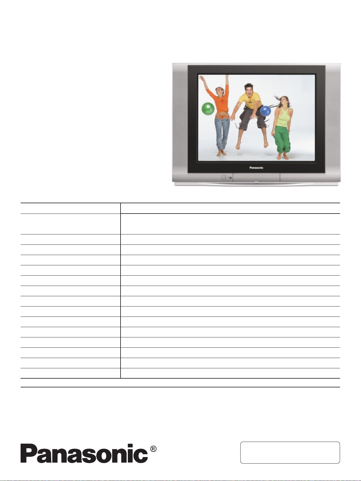
Color Television
TC-21FJ30LA
GP3 Chassis
Specifications
TELEVISOR
Power source
Consumption
Antenna input jack
Color systems
Tuning system
Channel capability
Picture Tube (visual diagonal)
Potência de áudio
Video input jack
Audio input jack
Video output jack
Audio output jack
DVD input jack
Dimension (width, height, depth)
TC-21FJ30LA
110V / 220V AC, 60Hz
automatic switch
90W
75Ω - VHF/UHF/CATV
PAL-M / NTSC / PAL-N
F.S.T.
2 to 13 (VHF), 14 to 69 (UHF) and 1 to 125 (Cable)
PANABLACK - 21” Flat CRT, 53 cm (NBR5258) - 51 cm diagonal visual
8 W + 8 W max (RMS)
1 (rear) + 1 (frontal)
1 (rear) + 1 (frontal)
1 (rear)
1 (rear) + 1 (headphone)
1 (rear)
648 x 472 x 488 mm
Weight
Specifications are subject to change without notice. Weight and dimensions shown are approximate.
REMOTE CONTROL TRANSMITER:
• Model: TNQ2B3302
• Power source: 3V (2 AA type batteries)
• Infrared Length: 9500 Å (angstron)
23,8 Kg
SUPPLIED ACCESSORIES:
• 1 Remote Control Transmitter
• 1 300Ω/75Ω Aerial Adaptor
• 2 “AA” type batteries
© 2004 Panasonic da Amazônia S/A.
CS Division
Technical Support
Page 2

TC-21FJ30LA
Important Safety Notice
Special components are used in this television set which are important for safety. These parts are identified on the schematic
diagram by the symbol . It is essential that these critical parts are replaced with the manufacturer’s specified replacement
parts to prevent X-ray radiation, shock, fire or other hazards. Do not modify the original design without manufacturer’s permission.
!
Contents
OPERATING INSTRUCTIONS ................................................................ 4
IC601 - PINOUT ................................................................................... 5
IC VOLTAGE TABLES .......................................................................... 6
IC601 - BLOCK DIAGRAM ................................................................... 7
GP3 CHASSI FEATURE SUMMAR Y ..................................................... 8
THE DAC CONTROL FUNCTIONS FOR THE GP3 CHASSIS ................... 9
SERVICE MODE:
HOW TO ENTER IN THE SERVICE MODE .............................................. 9
TO EXIT SERVICE MODE AND RETURN TO NORMAL MODE ................. 9
ADJUSTMENTS:
CHK1, CHK2, CHK3 and CHK4 ADJUSTMENTS OPTIONS ............... 9, 10
TEST AND MEASUREMENT EQUIPMENTS REQUIRED ......................... 10
1- RF AGC ADJUSTMENT .................................................................. 1 1
2- VIF DETECTOR OUTPUT LEVEL CONFIRMA TION ......................... 1 1
3- BUZZING CONFIRMATION (AUDIO CIRCUIT) ................................ 11
4- ANODE AND HEATER VOLT AGE CONFIRMA TION ........................ 11
5- PA L COLOR OUTPUT LEVEL ADJUSTMENT ................................ 12
6- NTSC SUB-TINT CALIBRATION ..................................................... 12
7- PROTECTION CIRCUIT (SHUTDOWN) OPERATION) ...................... 12
8- SUB-BRIGHTNESS AND SUB-CONTRAST CALIBRATION ............ 13
9- FOCUS CALIBRATION ................................................................... 13
10- COLOR PURITY ADJUSTMENT ...................................................... 13
11- WHITE QUALITY CALIBRATION .................................................... 14
12- CONVERGENCE CALIBRATION ..................................................... 14
13- CRT CUT OFF CALIBRATION ....................................................... 14
14- VERTICAL DEFLECTION CALIBRATION ........................................ 15
15- WITHE BALANCE CALIBRATION ................................................... 15
EEPROM MEMORY MAPS ................................................................... 16
SCHEMATICS DIAGRAMS:
MAIN PCB SCHEMATIC DIAGRAM ...................................................... 18
“L” CRT PCB SCHEMA TIC DIAGRAM .................................................. 19
“YUV” PCB SCHEMATICS DIAGRAMS ................................................ 20
MAIN PCB LAYOUT ............................................................................ 21
SIGNAL WA VEFORMS ........................................................................ 22
EXPLODED VIEW ................................................................................. 26
PARTS LISTS:
REPLACEMENT MECHANICAL P ARTS LIST ........................................ 27
REPLACEMENT ELECTRICAL P ARTS LIST .......................................... 28
General Guidelines
An Isolation Transformer should always be used during the servicing
of a receiver whose chassis is not isolated from the AC power line. Use
a transformer of adequate power rating as this protects the technician
from accidents resulting in personal injury from electrical shocks. It will
also protect the Receiver from being damaged by accidental shorting
that may occur during servicing.
When servicing, observe the original lead dress, especially in the high
voltage circuit. Replace all damaged parts (also parts that show signs
of overheating.)
Always Replace Protective Devices, such as fishpaper, isolation
resistors and capacitors, and shields after servicing the Receiver. Use
only manufacturer’s recommended rating for fuses, circuit breakers,
etc.
High potentials are present when this Receiver is operating. Operation
of the Receiver without the rear cover introduces danger from electrical
shock. Servicing should not be performed by anyone who is not
thoroughly familiar with the necessary precautions when servicing highvoltage equipment.
Extreme care should be practiced when Handling the Picture Tube.
Rough handling may cause it to implode due to atmospheric pressure
(14.7 lbs per sq. in). Do not sick or scratch the glass or subject it to any
undue pressure. When handling, use safety goggles and heavy gloves
for protection. Discharge the picture tube by shorting the anode to
chassis ground (not to the cabinet or to other mounting hardware).
When discharging, connect cold ground (i.e. dag ground lead) to the
anode with a well insulated wire or use a grounding probe.
Avoid prolonged exposure at close range to unshielded areas of the
picture tube to prevent exposure to X-ray radiation.
The Test Picture Tube used for servicing the chassis at the bench
should incorporate safety glass and magnetic shielding. The safety
glass provides shielding for the tube viewing area against X-ray radiation
as well as implosion. The magnetic shield limits X-ray radiation around
the bell of the picture tube in addition to restricting magnetic effects.
When using a picture tube test jig for service, ensure that the jig is
capable of handling 31kV without causing X-ray radiation.
Before returning a serviced receiver to the owner, the service technician
must thoroughly test the unit to ensure that is completely safe to operate.
Do not use a line isolation transformer when testing.
Warning !
It is essential that these critical parts are replaced
with the manufacturer’s specified replacement parts
!
to prevent X-ray radiation, shock, fire or other hazards.
- 2 -
Page 3
TC-21FJ30LA
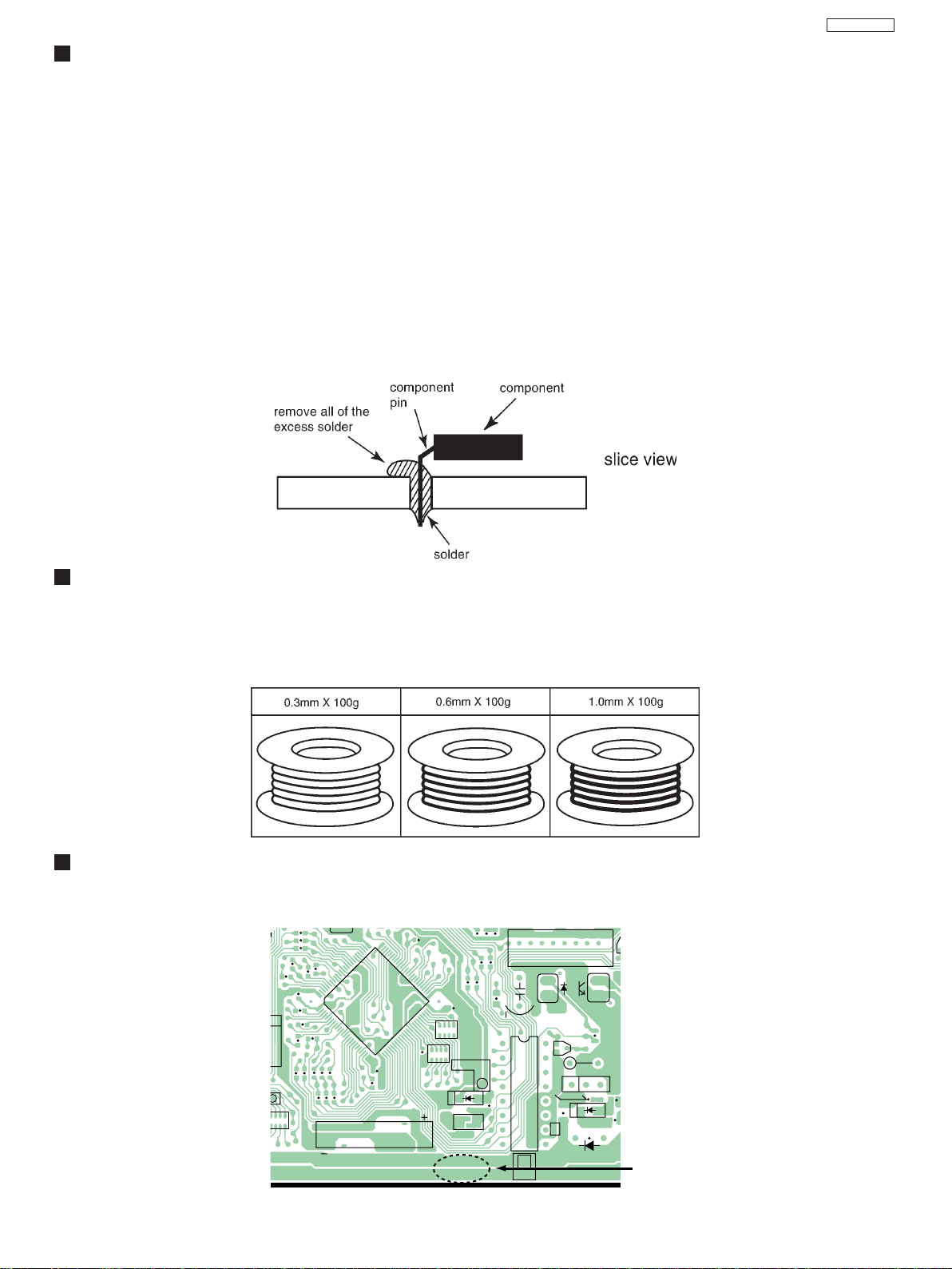
ABOUT LEAD FREE SOLDER (PbF)
Note:
In the information below, Pb, the symbol for lead in the periodic table of elements, will refer to standard solder or solder that
contains lead.
We will use PbF solder when discussing the lead free solder used in our manufacturing process which is made from Tin (Sn),
Silver, (Ag), and Copper, (Cu).
This model, and others like it, manufactured using lead free solder will have PbF stamped on the PCB. For service and repair
work we suggest using the same type of solder although, with some precautions, standard Pb solder can also be used.
Caution
• PbF solder has a melting point that is 50° ~ 70° F, (300° ~ 400°C) higher than Pb solder. Please use a soldering iron with
temperature control and adjust it to 700° ± 20° F, (370° ± 10°C).In case of using high temperature soldering iron, please be
careful not to heat too long.
• PbF solder will tend to splash if it is heated much higher than its melting point, approximately 1100°F, (600°C).
• If you must use Pb solder on a PCB manufactured using PbF solder, remove as much of the original PbF solder as possible
and be sure that any remaining is melted prior to applying the Pb solder.
• When applying PbF solder to double layered boards, please check the component side for excess which may flow onto the
opposite side (See figure, below).
SUGGESTED PbF SOLDER
There are several types of PbF solder available commercially. While this product is manufactured using Tin, Silver, and Copper,
(Sn+Ag+Cu), you can also use Tin and Copper, (Sn+Cu), or Tin, Zinc, and Bismuth, (Sn+Zn+Bi). Please check the manufac
turer’s specific instructions for the melting points of their products and any precautions for using their product with other
materials.
The following lead free (PbF) solder wire sizes are recommended for service of this product: 0.3mm, 0.6mm and 1.0mm.
HOW TO RECOGNIZE THAT PB FREE SOLDER IS USED
P.C.Boards marked as “PbF” use Pb Free solder. (See the figure below.) Pb Free is not used the Power Supply Board of this
unit.
(Example : Digital Board)
L624
L625
L626
L660
L661
L658
L659
100
C694
L653
L655
L657
L654
L656
1
L642
R768
L605
H
RA602
PFUP1330YA PbF
R767
R769
L606
L604
Q609
75
76
IC605
2625
C666
L643
BAT600
R70
C738
51
50
C667
RA609
D602
C668
RA610
C672
C731
L620
L619
L618
+3.3V/BAT
J600
C717
L621
R723
L630
1
R708
8
C728
IC610
+24V
CN612
16
9
Q613
E
R736
F605
25
18
R613R610
R611
R737
E
Q620
D608
C726
D607
Marked
DIGITAL BOARD COMPONENT VIEW
- 3 -
Page 4
TC-21FJ30LA
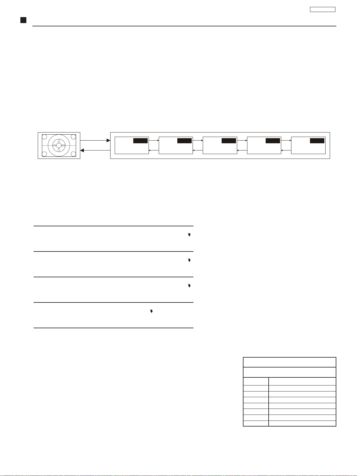
OPERATING INSTRUCTIONS
ACCESO DIRECTO
A LOS CANALES
6
R-TUNE
CLOSED CAPTION
CC
BOTONES DE
DIRECCIÓN
DEL MENÚ
+–
MAIN MENUPIC MENU
MAIN MENU
(MENÚ PRINCIPAL)
SELECCIÓN
SECUENCIAL DE
u
ENCIENDE/APAGA
CANALES
SURROUND
PLAY
STOP
123
u
Controle remoto
ENCIENDE/APAGA
890
45
7
t
SILENCIO
TIMER
WAKE-UP
TV/AV WAKE UP R-TUNE
TV/AV
(DESPERTADOR)
4
e
N
LLAMADA
NORMALIZACIÓN
Y3
VOLUMEN
Entradas de
Vídeo/Áudio
SURROUND
$
SOUND MENU
SAP
PIC MENU
(MENÚ DE IMAGEN)
Salida de
Áudio/Vídeo
Entradas
)/+
=/0
SAP
para DVD
DVD
SALTAR/BUSCA
SOUND MENU
(MENÚ DE SONIDO)
PARA ATRÁS
Panasonic
SALTAR/BUSCA
PARA ADELANTE
VistaTrasera de laTelevisión
Vista Frontal de laTelevisión
VIDEO
MONO
AV1 IN
Y
DVD OUT
Panasonic
AUDIO
L
R
B
R
P
P
L
R
AUDIO
Terminal
de la antena
2B052
TBM
2
R
AV2 IN
L/MONO
VIDEO AUDIO
ÚÙ
–+ç
PRE.TV/AV
u
LIGA/DESL
Interruptor
Apagado
Encendido/
Sensor
de Control
Remoto
Entrada
de alimentación
Salida del cable
Luz indicadora
de Áudio
Auriculares
Entrada
de Áudio
Entrada
de Vídeo
selección
Botones de
Volumen
Botones de
Botón
TV/AV
Botón de
PRE-AJUSTE
secuencial
de canales
R
L/MONO
2
DIO
AV2 IN
VIDEO AU
ÚÙ
E. TV/AV
PR
- 4 -
Page 5

TC-21FJ30LA
IC601 - PINOUT
Symbol Pin Description
P3.1/ADC1 1 port 3.1 or ADC1 input
P3.2/ADC2 2 port 3.2 or ADC2 input
P3.3/ADC3 3 port 3.3 or ADC3 input
VSSC/P 4 digital ground for m-Controller core and periphery
P0.5 5 port 0.5 (8 mA current sinking capability for direct drive of LEDs)
P0.6/CVBSTD 6 port 0.6 (8 mA current sinking capability for direct drive of LEDs) or Composite video input. A positive-going
1V (peak-to-peak) input is required
VSSA 7 digital ground of TV-processor
SECPLL 8 SECAM PLL decoupling
VP2 9 2nd supply voltage TV-processor (+8V)
DECDIG 10 supply voltage decoupling of digital circuit of TV-processor
PH2LF 11 phase-2 filter
PH1LF 12 phase-1 filter
GND3 13 ground 3 for TV-processor
DECBG 14 bandgap decoupling
EWD 15 East-West drive output
VDRB 16 vertical drive B output
VDRA 17 vertical drive A output
IFI N1 18 IF input 1
IFI N2 19 IF input 2
IREF 20 reference current input
VSC 21 vertical sawtooth capacitor
AGCOUT 22 tuner AGC output
SIFIN1 23 SIF input 1
SIFIN2 24 SIF input 2
GND2 25 ground 2 for TV processor
SNDPLL 26 narrow band PLL filter
AVL/REF0/SNDIF (1) 27 Automatic Volume Levelling / subcarrier reference output / sound IF input
AUDIO2 28 audio 2 input
AUDIO3 29 audio 3 input
HOUT 30 horizontal output
FBISO 31 flyback input/sandcastle output
DECSDEM 32 decoupling sound demodulator
QSSO/AMOUT/ 33 QSS intercarrier output / AM output in stereo applications or deemphasis
AUDEEM (1) (front-end audio out) / AM output in mono applications
EHTO 34 EHT/overvoltage protection input
PLLIF 35 IF-PLL loop filter
SIFAGC 36 AGC sound IF
INTCO 37 intercarrier output (from QSS or vision IF amplifier)
IFVO/SVO (1) 38 IF video output / selected CVBS output
VP1 39 main supply voltage TV processor
CVBS1 40 internal CVBS input
GND 41 ground for TV processor
CVBS2 42 external CVBS2 input
GND 43 ground for TV-processor
CVBS3/Y 44 CVBS3/Y input
C 45 chroma input
WHSTR 46 white stretch capacitor
CVBSO 47 CVBS output
AUDOUT /AMOUT 48 audio output /AM audio output (volume controlled)
SVM 49 scan velocity modulation output
INSSW2 50 2nd RGB / YUV insertion input
R2/VIN 51 2nd R input / V (R-Y) input / PR input
G2/YIN 52 2nd G input / Y input
B2/UIN 53 2nd B input / U (B-Y) input / PB input
BCLIN 54 beam current limiter input
BLKIN 55 black current input / V-guard input
RO 56 Red output
GO 57 Green output
- 5 -
Page 6
TC-21FJ30LA
IC601 - PINOUT
Symbol Pin Pin
BO 58 Blue output
VDDA 59 analog supply of Teletext decoder and digital supply of TV-processor (3.3 V)
VP E 60 OTP Programming Voltage
VDDC 61 digital supply to core (3.3 V)
OSCGND 62 oscillator ground supply
XTALIN 63 crystal oscillator input
XTALOUT 64 crystal oscillator output
RESET 65 reset
VDDP 66 digital supply to periphery (+3.3 V)
P1.0/INT1 67 port 1.0 or external interrupt 1 input
P1.1/T0 68 port 1.1 or Counter/Timer 0 input
P1.2/INT0 69 port 1.2 or external interrupt 0 input
P1.3/T1 70 port 1.3 or Counter/Timer 1 input
P1.6/SCL 71 port 1.6 or I2C-bus clock line
P1.7/SDA 72 port 1.7 or I2C-bus data line
P2.0/TPWM 73 port 2.0 or Tuning PWM output
P2.1/PWM0 74 port 2.1
P2.2/PWM1 75 port 2.2
P2.3/PWM2 76 port 2.3
P2.4/PWM3 77 port 2.4
P2.5/PWM4 78 port 2.5
SYNC_FILTER 79 CVBS (i.e. P0.6/CVBS) Sync filter input: This pin should be connected to VSSA via a 100 nF capacitor.
P3.0/ADC0 80 port 3.0 or ADC0 input
IC VOLTAGE TABLES
Pin Vol tage
1 3,3
2 21.2mV
32
40
5 2,56
6 97.5mV
70
8 2,3
98
10 5
11 3,3
12 3,9
13 0
14 4
15 11.6mV
16 1,3
17 1,3
18 1,9
19 1,9
20 3,9
21 3,8
22 146.7mV
23 181.3mV
24 181.3mV
25 0
26 1,3
27 2,5
28 3,7
29 3,7
30 0,6
31 0,5
32 2,3
33 2,8
34 1,6
35 1,5
36 198mV
37 0,4
38 2,7
39 8
40 3,6
IC601
Pin Vol tage
41 0
42 3,8
43 0
44 3,3
45 0
46 3,6
47 2,9
48 3,5
49 4,4
50 2,5
51 2,7
52 2,7
53 2,7
54 2
55 5,3
56 3
57 3
58 3
59 3,3
60 0
61 3,3
62 28.5mV
63 1,9
64 1,9
65 0
66 3,3
67 105mV
68 4,7
69 5
70 3,2
71 2,3
72 3
73 55.9mV
74 0
75 0
76 3,7
77 0
78 0
79 0
80 0
IC451
Pin Vol tage
1 0,3V
2 15,6V
3 -14V
4 -15,6V
5 67mV
6 16,5V
7 0,3V
IC1103
Pin Vol tage
1 7,3mV
2 7,3mV
3 7,3mV
4 7,3mV
5 3,8V
6 3,8V
7 0,2V
85V
TPA10 142V
TPA11 11,2V
IC801
Pin Vol tage
1 183V
20V
3 22,7V
4 22,3V
5 96mV
6 1,5V
7 0,52V
IC1201
Pin Vol t age
15V
2 6,4mV
3 1,27V
4 3,3V
5 6,4mV
65V
IC851
Pin Vol tage
1 10,5V
2 10,5V
3 6,5V
4 4,3mV
5 6,3V
68V
75V
T801
Pin Vol tage
(V2) 1 22,5mV
(V1) 2 23mV
(P2) 5 180V
(PT) 7 170V
(P1) 8 168V
(S6) 11 0,5V
(S1) 12 0,2V
(S2) 15 0,7V
(S3) 17 0,2V
X101
Pin Vol tage
1 0,25V
2 0,25V
3 1,9V
4 1,9V
IC802
Pin Vol tage
1 141V
2 8,5V
3 -8,7mV
Pin Vol tage
All voltage measurements were made in POWER ON mode, with 127V 60Hz power
source and Color Bars Video Pattern.
IC880
1 10,4V
25V
3 -3,9mV
- 6 -
Page 7
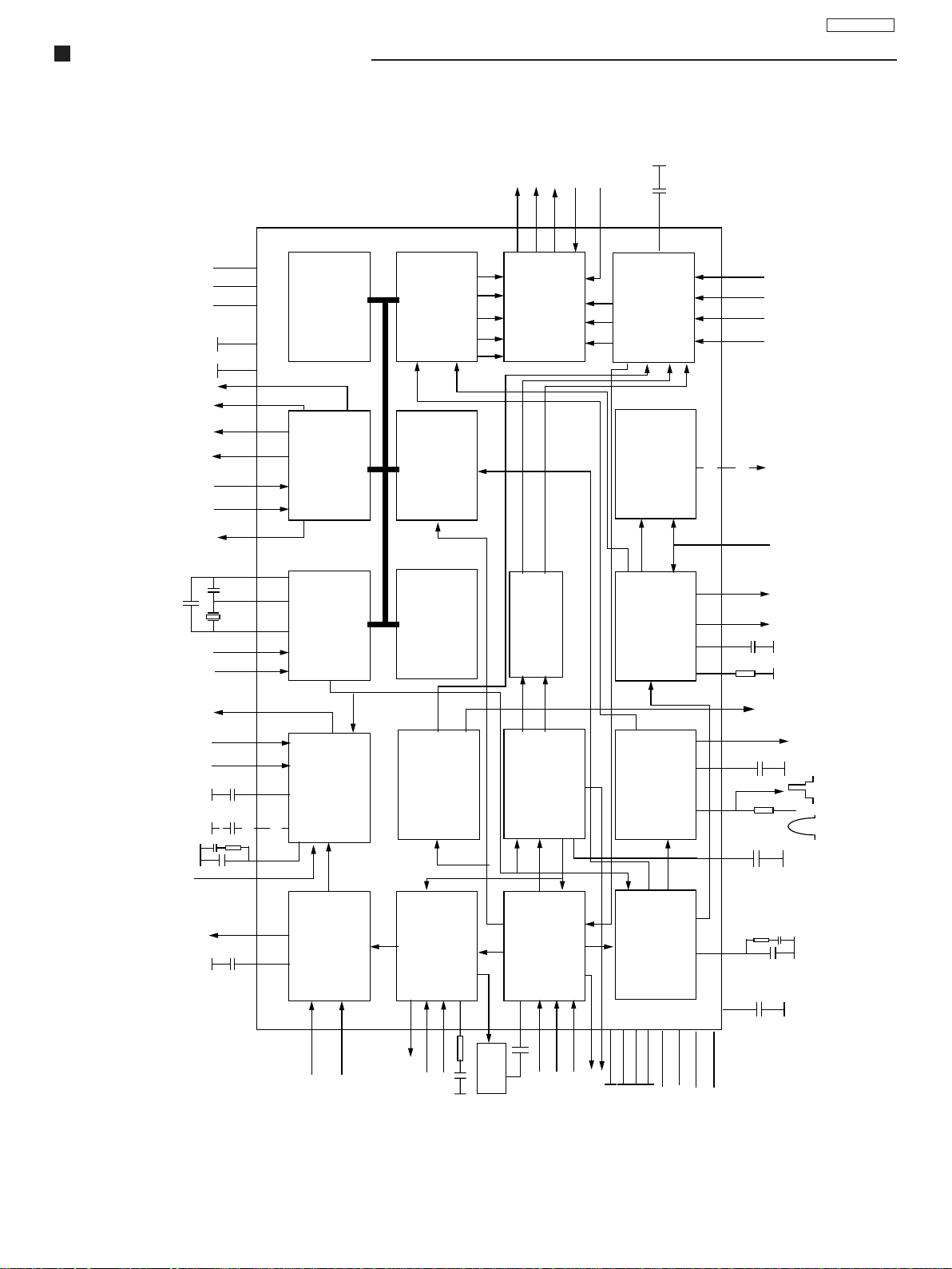
IC601 - BLOCK DIAGRAM
TC-21FJ30LA
+3.3 V
PWMS(4X)
I/O PORTS (4x)
ADC IN (4x)
VST OUT
SDASCL
LED OUT (2x)
VPE
RESET
AUDOUT
AUDIO3
AUDIO2
1/10 PAGE
MEMORY
C-BUS
2
I
TRANSCEIVER
VST PWM-DAC
80C51 CPU
ENHANCED
I/O PORTS
DISPLAY
TELETEXT/OSD
V
H
TELETEXT
ACQUISITION
CVBS
ROM/RAM
ROGOBO
BL
B
RG
CONTR/BRIGHTN
OSD/TEXT INSERT
COR
SYNC
DELAY LINE
BASE-BAND
BLKIN
BCLIN
GB
CCC
R
WHITE-P. ADJ.
BLUE STRETCH
TINT CONTROL
SATURATION
BLACK STRETCH
RGB/YUV INSERT
WHITE STRETCH
Y
U
V
EW GEOMETRY
V-DRIVE +
GEOMETRY
V
G/Y B/U BL
R/V
(EWD)
EHTO
VMOUT
HOUT V-DRIVE
(AVL)
(SNDIF)
AUDEEM
QSSO/AMOUT
AVL
SOUND PLL
DEEMPHASIS
AUDIO SWITCH
VOLUME CONTROL
AGC
QSS MIXER
QSS SOUND IF
AM DEMODULTOR
SIFIN
LUMA DELAY
REF
VISION IF
PLL DEMOD.
VIFIN
TUNERAGC
PEAKING
VMOUT
AGC/AFC
VIDEO AMP.
- 7 -
PAL/SECAM/NTSC
REF
VIDEO SWITCH
IFVO
TRAP
SOUND
DECODER
VIDEO IDENT.
VIDEO FILTERS
CVBS3/Y
CVBS2
C
CVBSO
Y
LOOP
nd
H-DRIVE
H-SHIFT
2
H
H-OSC. + PLL
H/V SYNC SEP.
+8V
Page 8
TC-21FJ30LA
CHASSIS GP3 FEATURE SUMMARY
CHASSIS : GP3
MODEL : TC-21FJ30LA
SYSTEM : (P AL-M/P AL-N/NTSC) (PAL-M 50Hz)
POWER SOURCE : AC automatic power switching 1 10/220V, 50/60Hz
MEMORY : 125 positions
TV TUNING RANGE : 181 channels (TV / CATV )
OSD LANGUAGE : Sp anish , Portuguese and English
AUDIO SYSTEM : Stereo
VERTICAL MAGNETIC FELD : -0.15 ±0.03 (ARGENTINA)
COLOR TEMPERATURE : (High Light) x= 0.275 ± 0.01, y=0.284 ± 0.01, Y=150 (nit))
(Low Light) x= 0.273 ± 0.01, y=0.283 ± 0.01, Y=7.0 (nit)
REFERENCE VOLTAGE
CONTENTS REFERENCE TEST POINT
+B VOLTAGE
Buzzing confirmation
PAL color output
NTSC color output
Anode (EHT) voltage
Memory Data
002
007
009
010
008
[A]=C4, [B]=00, [C]=00, [D]=33, [E]=03, [F]=20, [G]=00, [H]=09
TPA10
TPA8
TPA9
TPA21
A22-1 - A22-3
or A22-2 - A22-4
TPL2
TPL1
TPL1
ANODO
DO CRT
ADJUSTMENT
POINTS
D
C
C
SPECIFICATIONS
140 ± 1,5V
8 ±1V
5 ±1V
175 ±15V
0.5 Vp-p
2.45 ±0.1Vo-p
2.45 ±0.5Vo-p
1.2 ±0.5Vo-p
28,5 +0.7 (Kv)
28,5 -1.5 (kV)
- 8 -
Page 9
TC-21FJ30LA
Turn Off
NORMAL MODE
OPTION CODE
SETTING
“2”
“
1”
VCJ
ADJUSTMENT
CHK1
SERVICE MODE
“2”“2”
“
1”“1”
PINCUSHION
ADJUSTMENT
WHITE BALANCE
ADJUSTMENT
CHK2 CHK3
“2”
“
1”
STEREO
ADJUSTMENT
CHK4 CHK5
THE DAC CONTROL FOR GP3 CHASSIS FUNCTIONS AND ADJUSTMENTS
HOW TO ENTER IN THE SERVICE MODE:
1- Set the “OFF TIMER” to 30 minutes.
2- Press simultaneously “RECALL” key on the remote control and VOL(-) button on the unit.
After a couple of seconds, the expression “CHK” should appear on the right superior side of the screen. (T o change
the memory data, press MUTE and VOLUME(_) simultaneously while the OSD is still on CHK1 mode. Key “4” moves
forward in the memory , and key “3” moves back in the memory
Note: To alter from CHK1 mode to CHK2, CHK3 or CHK4 modes, press key “2” to move forward and the key “1” to
move back, as illustrated below.
TO EXIT SERVICE MODE AND RETURN TO NORMAL MODE:
Press the “NORMAL” key on the remote control unit or turn off the TV.
CHK1 - OPTIONS
On CHK1 mode, it is possible to adjust the options below:
“4”
OPTION1 OPTION1 OPTION2 OPTION2
DIGITO MSB DIGITO LSB DIGITO MSB DIGITO LSB
OPTION3
DIGITO MSB
OPTION5
DIGITO MSB
OPTION7
DIGITO MSB
ááá
“3”
“4”
á
OPTION3
á
DIGITO LSB
“3”
“4”
á
OPTION5
á
DIGITO LSB
“3”
“4”
á
OPTION8
á
DIGITO LSB
“3”
“4”
“3”
“4”
á
OPTION4
á
DIGITO MSB
“3”
“4”
á
OPTION6
á
DIGITO MSB
“3”
“4”
á
OPTION1
á
DIGITO MSB
“3”
“4”
“3”
“4”
á
OPTION4
á
DIGITO LSB
“3”
“4”
á
OPTION6
á
DIGITO LSB
“3”
“4”
å
“3”
“3”
“3”
“4”
“4”
“4”
“3”
å ááá
å
å
Note:
To select an option, type “4” to move forward
and “3” to move back.
After having selected the desired option, adjust
it by pressing the “VOL(_)” or “VOL(+)” keys.
Press “0” to memorize the adjustment.
CHK1 MODE - OPTIONS
On CHK1 mode it is possible to adjust the items of the table shown here.
Note:
To select an item, type “4” to move forward and “3” to move back.
After having selected the desired option, adjust it by pressing the “VOL(_)” or “VOL(+)”
keys. The OSD color will change for red.
Press “0” To memorize the adjustment.
CHK1 MODE T ABLE
Standard values
OPTION1
OPTION2
OPTION3
OPTION4
OPTION5
OPTION6
OPTION7
OPTION8
C4
00
00
33
03
20
00
09
- 9 -
Page 10
TC-21FJ30LA
ADJUSTMENTS
CHK2 MODE - VCJ ADJUSTMENTS
On CHK2 mode it is possible to adjust the items of the table shown here.
Note:
To select an item, type “4” to move forward and “3” to move back.
After having selected the desired option, adjust it by pressing the “VOL(_)” or “VOL(+)”
keys. The OSD color will change for red.
Press “0” To memorize the adjustment.
CHK3 MODE - PINCUSHION ADJUSTMENTS
On CHK3 mode it is possible to adjust the items of the table shown here.
Note:
To select an item, type “4” to move forward and “3” to move back.
After having selected the desired option, adjust it by pressing the “VOL(_)” or
“VOL(+)” keys. The OSD color will change for red.
Press “0” To memorize the adjustment.
V-SLOPE
V-SHIFT
V-AMP
H-SHIFT
S-CORR
CHK4 MODE - WHITE BALANCE ADJUSTMENTS
On CHK4 mode it is possible to adjust the items of the table shown here.
Note:
To select an item, type “4” to move forward and “3” to move back.
After having selected the desired option, adjust it by pressing the “VOL(_)” or
“VOL(+)” keys. The OSD color will change for red.
Press “0” To memorize the adjustment.
R-CUT
G-CUT
BRT
S-BRT
CONT
S-CONT
R-DRIVE
G-DRIVE
B-DRIVE
RGB CONTRASTE
CHK2 MODE T ABLE
Standard values
RF AGC
CONT
COL
S-COL
TINT
S-TINT
BRT
CHK3 MODE TABLE
Standard values
CHK4 MODE TABLE
Standard values
22
100
50
36
50
18
49
31
34
48
31
30
14
20
49
30
100
04
37
31
43
02
TEST AND MEASUREMENT EQUIPMENTS
T o execute all these electrical adjustments, the following equipment are required:
• Dual-Trace Oscilloscope
Volt age Range: 0.001 V to 50 V/Div.
Frequency Range: DC to 50 MHz
Probes: 10:1, 1:1
• NTSC Video Pattern Generator
• DVM (Digital Volt Meter)
• MTS/SAP Signal Generator
• (TV Multi-Channel Sound Modulator (U.S.A.))
• Plastic Tip Driver and Non-Metal Driver
• Isolation Transformer (V ariable)
• Degaussing Coil
• White Pattern Generator
• Audio Generator
- 10 -
Page 11

ADJUSTMENTS
ITEM / PREPARATION PROCEDURE
TC-21FJ30LA
1- RF AGC ADJUSTMENT
1. Supply a color bar pattern and adjust the RF input signal
of 69 dB µV (75Ω opened channel 07 RF freq.: 175.25
MHz).
2. Connect the digital multimeter in TPA15.
2- VIF DETECTOR OUTPUT LEVEL
CONFIRMATION
3- BUZZING CONFIRMATION
(AUDIO CIRCUIT)
1. Connect the oscilloscope with a 7kHz filter between A22-
2 and A22-3 speakers terminals .
2. Adjust the sound to maximum.
3. Adjust AVL: OFF
ADJUSTMENT:
1. Select “RF AGC” on “CHK2” service mode.
2. Adjust "RF AGC" by pressing VOL(+) or (-) until obtaining
2.2±0.1V in TPA15.
3. Increase the input level by +2 dB and confirm that the
voltage decreases in TPA15.
CONFIRMATION:
1. Install the chassis in the VIF calibration JIG and tune in a
63 dBU colorbar pattern (75Ω opened).
2. Connect the oscilloscope in TPA31.
3. Confirm that the output video sign is 1.05 ± 0.15 Vp-p in
TPA 31.
CONFIRMATION:
1. Supply a colorbar signal with local frequency adjusted
and the AFC ON (Channel with sound bearer and without
modulation).
2. Assure that the width in the buzzing waveform is smaller
than 500 m Vp-p.
4- ANODE AND HEATER VOLTAGE CONFIRMATION
1. Supply a crosshatch signal.
2. Adjust the current beam to zero. (0 beam).
3. Adjust “SCREEN VR” and “CONTRAST” to minimum.
Nota:
(When using a high voltage meter resistive type, it is
necessary to use an electrostatic meter type to verify the
values)
smaller than
500 m Vp-p
CONFIRMATION
1. Connect a voltage meter between TPA10 and ground.
Confirm that the voltage +B is within a range of 140.5V±
1.5V
2. Connect a high frequency voltage meter (VRMS) among
the heater, and confirm that the voltage is 6,30±0,24Vrms
3. Connect the high voltage meter in the CRT anode pin,
and confirm that the high voltage is within 30,5KV~27,6KV
range.
- 11 -
Page 12

TC-21FJ30LA
ADJUSTMENTS
ITEM / PREPARATION PROCEDURE
5- PAL COLOR OUTPUT SIGNAL ADJUSTMENT
1. Supply a color bar signal and adjust the local frequency.
2. Adjust “IMAGE” to DYNAMIC NORMAL, “CONTRAST” to
63 and “SUB-CONTRAST” to 21.
3. Adjust the “CHANNEL COLOR” level to NORMAL.
4. Set to CHK2 service mode option, press “5” on the remote
control unit and confirm that OSD becomes blue (AKB
turned off).
5. Set ABL to OFF (in CHK2 mode, to access BRT, CONT,
S-CONT or S-TINT).
6. Adjust [A] for 2.3 ± 0.2V through the BRIGHT control
variation in the test point TPL2.
7. Confirm that the RGB Contrast is 11DAC and {352} = 1B
8. Fix G-DRIVE GAIN, R-DRIVE GAIN and B-DRIVE GAIN
data in 1FH or 31 DAC.
R-DRIVE GAIN: [SLV(8A), SUB (16)]
G-DRIVE GAIN: [SLV(8A), SUB (17)]
B-DRIVE GAIN: [SLV(8A), SUB (18)]
6- NTSC SUB-TINT CALIBRA TION
1. Connect the oscilloscope in TPL1 (R-OUT) with a 10KΩ
resistor.
2. Supply a Rainbow signal (NTSC 3.58 MHz) through
VIDEO IN.
3. Select “IMAGE” to DYNAMIC NORMAL.
4. Select “COLOR FOR CHANNEL” to NORMAL.
5. On CHK2 service mode, press “5” (AKB OFF) and confirm
that OSD becomes blue (AKB turned off).
6. Set ABL to OFF (on CHK2 mode, to access BRT, CONT,
S-CONT or S-TINT).
CALIBRATION:
1. Connect the oscilloscope in TPL2 (G-OUT) with a 10KΩ
resistor and adjust “CONTRAST”, so that the [B] waveform
it is 2.3±0.1V with 14” CRT and 2.6±0.1V with 20” CRT.
2. Adjust “SUB-COLOR” to obtain 2,45±0.1V in [D]
according to fig. 1.
3. Connect the oscilloscope in TPL1 (R-OUT) with a 10KΩ
resistor and confirm that the [C] waveform it is 2.45±0.1V
according to fig. 2.
4. Press the key “5” (AKB ON) and confirm that OSD
becomes white.
Fig. 1
A = 2.3 ±0.1Vo-p
B = 2.4±0.1V
D = 2.45±0.1V
Fig. 2
A = 2.3 ±0.2Vo-p
C = 2.45±0.1V
CALIBRATION:
1. Adjust [C] for 5.0±0.2V through the BRIGHT control
variation (CHK2) according to fig. 1.
2. Adjust SUB TINT-NTSC so that the levels of positions 2, 3
and 4 of Fig. 1 in accordance with the Fig. 2.
3. Set ABL to ON.
4. Press “5” and confirm that OSD becomes white (AKB
turned on).
7- PROTECTION CIRCUIT (SHUTDOWN)
CONFIRMATION OF OPERA TION
1. Supply a crosshatch pattern signal and adjust the
CONTRAST and BRIGHT DAC controls to minimum.
(Ibeam=0 µA)
Fig. 1 Fig. 2
CONFIRMATION:
1. Connect the voltmeter in TPA22 and confirm that the
voltage is smaller than 18,7 V.
2. Connect a DC source in TPA22 and confirm that the
protection circuit doesn't act when the voltage is 19,5V.
3. Confirm that the protection circuit acts with smaller voltage
than21,5V.
- 12 -
Page 13

ADJUSTMENTS
ITEM / PREPARATION PROCEDURE
TC-21FJ30LA
8- SUB-BRIGHT AND SUB-CONTRAST
CALIBRATION
1. Supply a WINDOW pattern signal.
2. Adjust IMAGE MENU to DYNAMIC NORMAL
9- FOCUS CALIBRATION
• Assure that the SUB-BRIGHTNESS adjustment has been
done.
1. Supply a Philips or monoscope pattern signal.
2. Adjust IMAGE MENU to DYNAMIC NORMAL.
SUB-BRIGHT CALIBRATION
1. Position the color analyzer in the LOW LIGHT image
area.
2. Ajust S-BRT <CHK 4> control, so that it is Y=0,7±0.2.
SUB-CONTRAST CALIBRA TION
1. Position the color analyzer in the HIGH LIGHT image
area.
2. Ajust S-CONT <CHK 4> DAC control, so that it is
Y=230±20.
3. If impossible to obtain that adjustment, adjust SUBCONT <CHK 4> again.
4. Check the SUB-BRIGHT adjust.
CALIBRATION:
1. Adjust the FOCUS variable resistor for the point of better
adjustment.
• with PHILIPS signal .... take as reference for adjustment
the third vertical line (fig. 1).
• with MONOSCOPE signal in the number 4 (fig.2).
4
1 2 3
Fig. 1
3 2 1
10- PURITY CALIBRA TION
1. Adjust the HELMHOLTZ device for the local magnetic field
(HORIZONTAL: 0 ± 0.03 X 10⁻⁴T)
2. Let the set warm up (aging time) for a minimum of 60
minutes.
3. Supply a purity pattern (white pattern).
4. Adjust CONTRAST and BRIGHT to MAXIMUM.
5. The static convergence adjustment must have been
made preliminarily.
6. Connect a DC ampere meter between FBT pin11 (-) and
FBT pin3 (+), and adjust to 1200mA±10%, varying the SBRT DAC control.
Fig. 2
CALIBRA TION:
1. Position the “ears” of the purity magnets both upward.
2. Adjust the purity until the markers in the purity jig
monitorscope becomes symmetrical in the horizontal
direction.
3. The vertical centralization correction is made through
the purity magnets for stripe CRT type only.
4. Slide the yoke forward by 10 mm±5 in the monitor. Then,
tighten the deflection yoke.
5. Repeat the procedures 2 ~ 4.
6. Press the belt of deflection yoke.
7. Adjust “beam landing” using a microscope. (for model
change or instrument check only)
- 13 -
Page 14

TC-21FJ30LA
ADJUSTMENTS
ITEM / PREPARATION PROCEDURE
11- WHITE QUALITY CALIBRATION
PREPARATION:
1. Adjust the HELMHOLTZ device to local magnetic field. Horizontal: 0 ± 0.003 x 10
2. Receive a white purity pattern.
3. Adjust CONTRAST and BRIGHT controls to maximum.
4. Previously adjust the CONVERGENCE.
5. Fully degauss the CRT by using an external degaussing
coil.
-4
T
12- CONVERGENCE CALIBRATION
1. Adjust the HELMHOLTZ device to local magnetic field.
2. Receive a crosshatch pattern.
3. Adjust IMAGE menu to DINÂMIC NORMAL and the DAC
BRIGHT control for the crosshatch pattern to be gray.
4. Remove the DY wedges and slightly tilt the deflection
yoke to the vertically and horizontally to obtain the good
overall convergence.
5. If purity error is found, repeat “Color Purity” adjustment
CALIBRATION:
1. Adjust the magnetic field in 0.4x10⁻⁴T (400 mG), and
check the white quality with the CRT turned to EAST and
to WEST .
2. Receive a red pattern, adjust the COLOR control to
maximum and confirm the purity adjustment.
3. If purity error is found at the CRT corners, apply magnetic
tapes to correct it, fully degauss the CRT again and repeat
the steps 1 and 2. Don't use this magnetic tapes on the
internal side of the yoke.
4. Receive a white purity pattern, adjust the COLOR control
to minimum and confirm the purity adjustment.
CALIBRA TION
Static convergence calibration
l) Assure that the magnets are positioned according to
illustration 1.
ll) Adjust the 4 poles magnets to align the R and B
CENTRAL DOTS and adjust the 6 poles magnets to
align both DOTS with G.
lll) After adjustment above, assure that the magnets are
sealed, through the application of white glue.
4 poles magnets (G-3)
6 poles magnets (R-G-B)
13- CRT CUT OFF CALIBRATION
1. Supply a WINDOWS signal.
2. Position DACs with the data below:
BRT —> 50H
S-BRT —> 31H
RGB CONTRAST —> 11DAC
SUB-CONTRAST —> 21H
R,G ,B DRIVE —> 31H
R,G CUT —> 31H
Note:
The electron beams are moved rotationally when the
static convergence magnets are rotated.
The reduction of rotational beams differ depending of
the two magnets angle. Therefore, it is necessary to
repeat the magnets calibrations sometimes, until
obtaining a good alignment.
CALIBRATION:
1. Press “5” (AKB OFF) and confirm that OSD becomes
blue.
2. Connect the oscilloscope in TPL5 and adjust BRT to
obtain 130V as in the Fig. 1 below.
3. Adjust the SCREEN to obtain a horizontal fine line in the
screen center.
Y = 1.0 +1.0 -0.5
4. Press “5” (AKB ON) and confirm that OSD becomes
white.
- 14 -
Fig. 1
Page 15

ADJUSTMENTS
ITEM / PREPARATION PROCEDURE
TC-21FJ30LA
14- VERTICAL DEFLECTION CALIBRA TION AND
CONFIRMATION
1. Adjust IMAGE to DYNAMIC NORMAL
Fig. 1
S-CORR CONFIRMA TION AND CALIBRA TION
1) Confirmation in 50Hz
1. Supply a PHILIPS PAL-N signal.
2. Confirm that S-CORR 50Hz is in 33 DAC .
2) Confirmation in 60Hz
1. Supply a MONOSCOPE signal.
2. Confirm that S-CORR 60Hz is in 33 DAC.
3) V-SLOPE calibration
1. Supply a MONOSCOPE signal.
2. Adjust V_SLOPE (CHK3) so that the beginning of the
black part of the image is aligned with the center of the
CRT as Fig. 1.
4) VERTICAL CENTRALIZATION 50 HZ CALIBRA TION
1. Supply a PAL-N Philips signal.
2. Adjust V-SHIFT 50Hz (CHK3) so that the Philips pattern’s
center it is in the center of the CRT.
5) VERTICAL CENTRALIZATION 60 HZ CALIBRA TION
1. Supply a MONOSCOPE signal.
2. Adjust V-SHIFT 60Hz (CHK3) so that the monoscope
pattern´s center it is in the center of the CRT.
6) VERTICAL HEIGHT (V-AMP 50HZ) CALIBRA TION
1. Supply a PHILIPS PAL-N signal.
2. Adjust V-AMP-50Hz (CHK3) so that the Philips pattern’s
circle height be the same dimension of the width.
7) VERTICAL HEIGHT (V-AMP 60HZ) CALIBRA TION
1. Supply a MONOSCOPE signal.
2. Adjust V-AMP-60Hz (CHK3) according to box.
3. MEMORIZE in EEPROM.
C,D
A,B
Fig. 2
15- WHITE BALANCE CALIBRA TION
1. Adjust the HELMHOLTZ device to local magnetic field.
2. Let the set warm up for a minimum of 30 minutes.
3. Receive a white balance. (This sign should contain
burst sign).
4. Adjust the IMAGE menu to DINÂMIC NORMAL.
5. Fully degauss the CRT by using an external degaussing
coil.
6. Position the color analyzer in contact with the CRT face.
Assure that not entering light for the meter borders and that the CUT OFF voltage calibration has been done. If the value in the
color analyzer is below 150, adjust CONTRAST to 50 and press “8” in CHK2 mode.
CALIBRATION:
[1] LOW LIGHT CALIBRATION
1. Adjust S-BRT, so that Y = 7
2. Adjust R-CUT OFF, so that x = 0.273 ±0.01
3. Adjust G-CUT OFF, so that y = 0,283 ±0.01
[2] HIGH LIGHT CALIBRATION
(Confirm that G-DRIVE is 31 DAC)
1. Adjust S-BRT, so that Y = 150
2. Adjust R-DRIVE, so that x = 0,275 ±0.01
3. Adjust B-DRIVE, so that y = 0,284 ±0.01
[3] Repeat the procedures [1] and [2].
- 15 -
1.5 ~ 2.0
1.5 ~ 1.6
Page 16

TC-21FJ30LA
EEPROM MEMORY MAPS
TABLE 0
COLUNA COLUNA COLUNA COLUNA COLUNA COLUNA COLUNA COLUNA COLUNA COLUNA COLUNA COLUNA COLUNA COLUNA COLUNACOLUNA
0123456789ABCDEF
LINHA
0 02 00 06 01 00 06 02 00 06 03 00 06 04 00 06 05
LINHA
1 00 06 06 00 06 07 00 06 08 00 06 09 00 06 0A 00
LINHA
2 06 0B 00 06 0C 00 06 0D 00 06 0E 00 06 0F 00 06
LINHA
3 10 00 06 11 00 06 12 00 06 13 00 06 14 00 06 15
LINHA
4 00 06 16 00 06 17 00 06 18 00 06 19 00 06 1A 00
LINHA
5 06 1B 00 06 1C 00 06 1D 00 06 1E 00 06 1F 00 06
LINHA
6 20 00 06 21 00 06 22 00 06 23 00 06 24 00 06 25
LINHA
7 00 06 26 00 06 27 00 06 28 00 06 29 00 06 2A 00
LINHA
8 06 2B 00 06 2C 00 06 2D 00 06 2E 00 06 2F 00 06
LINHA
9 30 00 06 31 00 06 32 00 06 33 00 06 34 00 06 35
LINHA
A 00 06 36 00 06 37 00 06 38 00 06 39 00 06 3 A 00
LINHA
B 06 3B 00 06 3C 00 06 3D 00 06 3E 00 06 3F 00 06
LINHA
C 40 00 06 41 00 06 42 00 06 43 00 06 44 00 06 45
LINHA
D 00 06 46 00 06 47 00 06 48 00 06 49 00 06 4 A 00
LINHA
E 06 4B 00 06 4C 00 06 4D 00 06 4E 00 06 4F 00 06
LINHA
F 50 00 06 51 00 06 52 00 06 53 00 06 54 00 06 55
TABLE 1
COLUNA COLUNA COLUNA COLUNA COLUNA COLUNA COLUNA COLUNA COLUNA COLUNA COLUNA COLUNA COLUNA COLUNA COLUNA COLUNA
0123456789ABCDEF
LINHA
0 00 06 56 00 06 57 00 06 58 00 06 59 00 06 5A 00
LINHA
1 06 5B 00 06 5C 00 06 5D 00 06 5E 00 06 5F 00 06
LINHA
2 60 00 06 61 00 06 62 00 06 63 00 06 64 00 06 65
LINHA
3 00 06 66 00 06 67 00 06 68 00 06 69 00 06 6A 00
LINHA
4 06 6B 00 06 6C 00 06 6D 00 06 6E 00 06 6F 00 06
LINHA
5 70 00 06 71 00 06 72 00 06 73 00 06 74 00 06 75
LINHA
6 00 06 76 00 06 77 00 06 78 00 06 79 00 06 7A 00
LINHA
7 06 7B 00 06 7C 00 06 7D 00 06 0F 00 00 FF 01 0E
LINHA
8 00 00 00 00 00 00 00 00 00 00 00 00 00 00 00 00
LINHA
9 00 00 00 00 00 00 00 00 00 00 00 00 00 00 00 00
LINHA
A 06 00 00 00 00 00 00 00 00 00 01 02 01 02 03 04
LINHA
B 01 86 04 C4 00 00 37 8F 9F 8F 02 02 02 02 02 02
LINHA
C 02 02 5E 5E 60 40 D0 C0 A0 0A 08 18 1D 04 00 00
LINHA
D C8 C8 C8 C2 C2 C2 40 40 00 00 00 00 00 00 00 00
LINHA
E 00 00 00 00 00 00 00 00 00 00 00 00 00 00 00 00
LINHA
F 00 00 00 00 00 00 00 00 00 00 00 00 00 00 00 00
- 16 -
Page 17

TABLE 2
COLUNA COLUNA COLUNA COLUNA COLUNA COLUNA COLUNA COLUNA COLUNA COLUNA COLUNA COLUNA COLUNA COLUNA COLUNA COLUNA
0123456789ABCDEF
LINHA
0 02 00 A5 5A 00 01 01 00 00 08 00 03 09 09 03 00
LINHA
1 02 00 00 00 00 00 10 0C 0B 10 18 0B 0C 0C 0C 0B
LINHA
2 00 00 00 00 00 00 00 00 00 00 00 00 00 00 00 00
LINHA
3 00 00 00 00 00 00 00 00 00 00 00 00 00 00 00 00
LINHA
4 00 00 00 00 00 00 00 00 00 00 00 00 00 00 00 00
LINHA
5 32 32 32 64 4B 32 32 32 4B 44 2D 32 32 41 32 32
LINHA
6 18 0B 09 0D 14 3C D0 0D 00 0C 04 04 16 00 FC 0E
LINHA
7 00 00 00 00 00 00 00 00 00 00 00 00 03 02 78 BB
LINHA
8 32 32 32 64 4B 32 32 32 4B 44 2D 32 32 41 32 10
LINHA
9 0C 0B 10 18 0B 0C 0C 0C 0B 18 0B 09 0D 14 00 00
LINHA
A 00 00 00 00 00 00 00 00 00 00 00 00 00 00 00 03
LINHA
B 00 00 00 0C 00 1B 0C 08 1C 40 40 40 00 00 00 00
LINHA
C 00 00 00 00 00 00 00 00 00 00 00 00 00 00 00 00
LINHA
D 0C 10 15 04 06 06 00 04 00 00 00 00 00 00 00 00
LINHA
E 00 00 00 00 00 00 00 00 C4 00 00 33 03 20 00 09
LINHA
F 00 00 18 20 15 1 A 00 00 00 00 00 00 00 A5 3F A5
TC-21FJ30LA
TABLE 3
COLUNA COLUNA COLUNA COLUNA COLUNA COLUNA COLUNA COLUNA COLUNA COLUNA COLUNA COLUNA COLUNA COLUNA COLUNA COLUNA
0123456789ABCDEF
LINHA
0 00 00 00 00 00 00 00 00 00 00 00 00 00 00 00 00
LINHA
1 00 00 00 00 00 00 00 00 00 00 00 00 00 00 00 00
LINHA
2 00 00 00 00 00 30 30 C0 A4 94 22 88 28 20 31 24
LINHA
3 00 00 25 1D 21 16 1E 33 21 25 19 19 1F 1F 1F 1F
LINHA
4 1F 00 06 00 FD 00 1B 29 80 00 2A 00 34 20 30 21
LINHA
5 02 48 12 44 00 80 34 03 F4 FD 00 00 00 00 03 08
LINHA
6 04 FE 32 00 20 19 00 00 00 00 00 00 00 00 00 00
LINHA
7 00 00 00 00 00 00 00 00 00 10 00 00 00 00 00 00
LINHA
8 00 00 00 00 00 00 00 00 0E 11 0D 06 0C 0C 07 02
LINHA
9 09 00 00 FA 00 00 00 0A F8 00 00 00 00 00 00 03
LINHA
A 01 03 02 03 03 00 34 28 28 28 20 63 03 10 03 00
LINHA
B CA 49 4B 02 31 00 00 FF FD 04 05 FF 03 F5 FE 04
LINHA
C 20 07 4F 40 40 00 00 00 00 00 00 00 00 00 00 00
LINHA
D 05 0A 05 F7 FE FE 00 00 00 F7 00 F0 01 00 00 00
LINHA
E 10 04 2F 71 75 3B 3A 02 02 0E 3A 37 00 11 0B 05
LINHA
F 33 30 2A 27 26 25 24 00 00 00 00 00 00 00 00 11
- 17 -
Page 18

TC-21FJ30LA
Page 19

SCHEMA TICS DIAGRAMS
“L” P.C.B. SCHEMATIC DIAGRAM
TC-21FJ30LA
IC351
TDA6107JF/N3
TNP4G276-6
CRT CIRCUIT
JK351
L5L8
- 19 -
Page 20

TC-21FJ30LA
“YUV” P.C.B. SCHEMATIC DIAGRAM
- 20 -
Page 21

MAIN BOARD CIRCUIT LAYOUT
TC-21FJ30LA
- 21 -
Page 22

TC-21FJ30LA
SIGNAL WAVEFORM
• All waveforms were obtained using 127V 60Hz power source and Color Bars Pattern (Model: TC-20KL04)
IC451
IC601
Pino 1
Pino 7
Pino 5
Pino 16 Pino 17
- 22 -
Page 23

IC601
TC-21FJ30LA
Pino 18 Pino 19
Pino 38
Pino 42 Pino 55
Pino 40
- 23 -
Page 24

TC-21FJ30LA
IC601
Pino 56 Pino 57
Pino 58 Pino 63
Pino 64
- 24 -
Page 25

TC-21FJ30LA
IC801
Q501
Pino 1
Q551
Coletor
Q601
Base
Emissor
Coletor
Q602
Coletor
- 25 -
Page 26

TC-21FJ30LA
EXPLODED VIEW
1
16
17
10
7
15
8
2
11
12
2
11
9
13
11
14
5
4
6
11
- 26 -
3
Page 27

REPLACEMENT MECHANICAL PARTS LIST
TC-21FJ30LA
Ref. No.
1 A51QDX993X004 PICTURE TUBE 21" (FLAT SAMSUNG)
2 TKK4G8597 SPEAKER SUPPORT
3 EASG15S02H2 SPEAKER
4 TBM4G3013 PANASONIC LOGO
5 TBX4G9011 0 POWER BUTTON
6 TKP4G13030 CONTROL PANEL DOOR
7 T-TKU2B22702 REAR COVER
8 TLK4G9037X DEGAUSSING COIL
9 TKP4G13062 LED GUIDE
10 TKY2B2201-1 FRONTAL CABINET
1 1 TBL4G3407 LEG CUSHION
12 TES4G214 POWER BUTTON SPRING
13 TBM2B053-1 CONTROL PANEL
14 TNQ2B3302 REMOTE CONTROL
15 S-U5012 ADAPTOR BALLUM 300Ω
16 TSX2BA04 AC CABLE
17 TXPTKY2B2201-1 FRONTAL CABINET ASS´Y
Part No.
Part Name & Description
- 27 -
Page 28

TC-21FJ30LA
REPLACEMENT ELECTRICAL PARTS LIST
Ref. No.
FULLY ASSEMBLED BOARDS
“A” PAL21FJ30LAMON “A”+“L” P.C.B. ASS´Y
“YUV” PYUV20KM04MON “ YUC” P.C.B. ASS´Y
CAPACITORES
C001 ECEA1CKA220B ELECTROLYTICAL CAP. 22,00 µF 16,0 V
C002 ECJ2VF1H103Z CERAMIC CAP. 10,00 nF 50,0 V
C003 ECJ2VF1H103Z CERAMIC CAP. 10,00 nF 50,0 V
C005 ECJ2VF1H104Z CERAMIC CAP. 100,00 nF 50,0 V
C006 F2A1A331A161 ELECTROLYTICAL CAP. 330,00 µF 10,0 V
C008 ECEA1HKA010B ELECTROLYTICAL CAP. 1,00 µF 50,0 V
C117 ECJ2VB1H103J CERAMIC CAP. 10,00 nF 50,0 V
C180 ECJ2VC1H151J CERAMIC CAP. 150,00 PF 50,0 V
C191 ECJ2YB1H104K CERAMIC CAP. 100,00 nF 50,0 V
C193 F2A1C100A180 ELECTROLYTICAL CAP. 10,00 µF 16,0 V
C350 F2A1C101A180 ELECTROLYTICAL CAP. 100,00 µF 16,0 V
C354 ECJ2VC1H330J CERAMIC CAP. 33,00 PF 50,0 V
C355 ECJ2VC1H330J CERAMIC CAP. 33,00 PF 50,0 V
C356 ECJ2VC1H330J CERAMIC CAP. 33,00 PF 50,0 V
C359 ECQM4104KZB POLYESTER CAP. 100,00 nF 400,0 V
C368 ECJ2VC1H122J CERAMIC CAP. 1,20 nF 50,0 V
C370 ECKW3D102KBP CERAMIC CAP. 1,00 nF 2.000,0 V
C371 ECEA1CN100UB ELECTROLYTICAL CAP. 10,00 µF 16,0 V
C373 F2A2E1000011 ELECTROLYTICAL CAP. 10,00 µF 250,0 V
C377 F2A1C101A180 ELECTROLYTICAL CAP. 100,00 µF 16,0 V
C402 F2A1H1010039 ELECTROLYTICAL CAP. 100,00 µF 50,0 V
C403 F2A1H220A182 ELECTROLYTICAL CAP. 22,00 µF 50,0 V
C404 ECQB1103JF3 POLYESTER CAP. 0,01 µF 100,0 V
C406 ECA1HHG221B ELECTROLYTICAL CAP. 220,00 µF 50,0 V
C408 ECQB1274JF3 POLYESTER CAP. 270,00 nF 100,0 V
C502 F1B2H821A025 CERAMIC CAP. 820,00 PF 500,0 V
C503 F1B2H821A025 CERAMIC CAP. 820,00 PF 500,0 V
C504 ECJ2VB1H681K CERAMIC CAP. 680,00 PF 50,0 V
C506 F1A2H1000002 CERAMIC CAP. 10,00 PF 500,0 V 0,50 PF
C511 F2A1V1010038 ELECTROLYTICAL CAP. 100,00 µF 35,0 V
C513 ECKW3D331JBP CERAMIC CAP. 330,00 PF 2.000,0 V
C514 F2A1E102A151 ELECTROLYTICAL CAP. 1.000,00 µF 25,0 V
C515 F1B2H331A025 CERAMIC CAP. 330,00 PF 500,0 V
C516 F2A1E102A151 ELECTROLYTICAL CAP. 1.000,00 µF 25,0 V
C519 F2A2C330A020 ELECTROLYTICAL CAP. 33,00 µF 160,0 V
C520 F2A0J221A181 ELECTROLYTICAL CAP. 220,00 µF 6,3 V
C552 F2A2E1000011 ELECTROLYTICAL CAP. 10,00 µF 250,0 V
C555 F1B2H471A025 CERAMIC CAP. 470,00 PF 500,0 V
C558 ECQB1104JF3 POLYESTER CAP. 100,00 nF 100,0 V
C559 ECWH16752JVB POLYPROPILENE CAP. 7,50 nF 1.600,0 V
C560 ECQM4333JZW POLYESTER CAP. 33,00 nF 400,0 V
C561 ECKW3D271KBR CERAMIC CAP. 270,00 PF 2.000,0 V
C562 ECKW3D152JBR CERAMIC CAP. 1,50 nF 2.000,0 V
C563 ECWF2224JSR POLYPROPILENE CAP. 220,00 nF 250,0 V
C565 ECQP1H183JZ3 POLYPROPILENE CAP. 18,00 nF 50,0 V
C568 ECWH16332JVB POLYPROPILENE CAP. 3,30 nF 1.600,0 V
C570 ECJ2VC1H330J CERAMIC CAP. 33,00 PF 50,0 V
C580 F2A1H220A182 ELECTROLYTICAL CAP. 22,00 µF 50,0 V
C581 ECQV1H105JL3 POLYESTER CAP. 1,00 µF 50,0 V
C601 ECEA1CKA101B ELECTROLYTICAL CAP. 100,00 µF 16,0 V
C602 ECJ2YB1H104K CERAMIC CAP. 100,00 nF 50,0 V
C603 ECJ2VB1H472K CERAMIC CAP. 4.700,00 PF 50,0 V
C604 ECQV1H224JL3 POLYESTER CAP. 220,00 nF 50,0 V
C605 ECQV1H224JL3 POLYESTER CAP. 220,00 nF 50,0 V
C606 ECJ2VC1H222J CERAMIC CAP. 2.200,00 PF 50,0 V
C607 ECEA1HKA010B ELECTROLYTICAL CAP. 1,00 µF 50,0 V
C608 ECEA1HKA100B ELECTROLYTICAL CAP. 10,00 µF 50,0 V
C609 ECJ2YB1H104K CERAMIC CAP. 100,00 nF 50,0 V
C610 ECJ2VB1H103J CERAMIC CAP. 10,00 nF 50,0 V
C612 ECJ2VB1H472K CERAMIC CAP. 4.700,00 PF 50,0 V
C613 ECJ2VB1H472K CERAMIC CAP. 4.700,00 PF 50,0 V
C614 ECQV1H104JL3 POLYESTER CAP. 100,00 nF 50,0 V
C615 ECQV1H224JL3 POLYESTER CAP. 220,00 nF 50,0 V
C619 ECQV1H104JL3 POLYESTER CAP. 100,00 nF 50,0 V
C620 ECJ2VC1H470J CERAMIC CAP. 47,00 PF 50,0 V
C621 ECJ2VB1H471K CERAMIC CAP. 470,00 PF 50,0 V
C622 ECJ2VF1H104Z CERAMIC CAP. 100,00 nF 50,0 V
C623 ECJ2VC1H470J CERAMIC CAP. 47,00 PF 50,0 V
C625 ECEA0JN221UB ELECTROLYTICAL CAP. 220,00 µF 6,3 V
Part No.
Part Name & Description
Ref. No.
C628 ECJ2YB1H473K CERAMIC CAP. 47,00 nF 50,0 V
C631 ECJ2VB1H222K CERAMIC CAP. 2.200,00 PF 50,0 V
C632 ECJ2VB1H392K CERAMIC CAP. 3.900,00 PF 50,0 V
C633 ECJ2VF1C105Z CERAMIC CAP. 1,00 µF 16,0 V
C636 F2A1C101A180 ELECTROLYTICAL CAP. 100,00 µF 16,0 V
C640 F2A1C100A180 ELECTROLYTICAL CAP. 10,00 µF 16,0 V
C641 ECJ2VC1H100C CERAMIC CAP. 10,00 PF 50,0 V
C670 F2A1C100A180 ELECTROLYTICAL CAP. 10,00 µF 16,0 V
C680 ECJ2YB1H473K CERAMIC CAP. 47,00 nF 50,0 V
C685 ECJ2VC1H101J CERAMIC CAP. 100,00 PF 50,0 V
C686 ECJ2YB1H473K CERAMIC CAP. 47,00 nF 50,0 V
C687 ECJ2VF1H104Z CERAMIC CAP. 100,00 nF 50,0 V
C689 ECJ2VF1H104Z CERAMIC CAP. 100,00 nF 50,0 V
C801 ECQU2A224BN9 POLYPROPILENE CAP. 220,00 nF 100,0 V
C806 ECKWAE472ZED CERAMIC CAP. 4,70 nF 250,0 V
C807 ECKWAE472ZED CERAMIC CAP. 4,70 nF 250,0 V
C808 ECKWAE472ZED CERAMIC CAP. 4,70 nF 250,0 V
C809 ECKWAE472ZED CERAMIC CAP. 4,70 nF 250,0 V
C810 EETHC2G221C: ELECTROLYTICAL CAP. 220,00 µF 400,0 V
C811 ECQM4473JZW POLYESTER CAP. 47,00 nF 400,0 V
C814 ECQE2A473JFB POLYESTER CAP. 47,00 nF 250,0 V
C816 F2A1H330A115 ELECTROLYTICAL CAP. 33,00 µF 50,0 V
C816 F2A1V100A096 ELECTROLYTICAL CAP. 10,00 µF 35,0 V
C816 F2A1V100A096 ELECTROLYTICAL CAP. 10,00 µF 35,0 V
C819 F2A1H1R00053 ELECTROLYTICAL CAP. 1,00 µF 50,0 V
C821 ECKW3D471JBR CERAMIC CAP. 0,47 nF 2.000,0 V
C822 ECKW3D331JBR CERAMIC CAP. 330,00 PF 2.000,0 V
C825 ECQB1H471JF3 POLYESTER CAP. 470,00 PF 50,0 V
C826 F0A1H103A039 POLYPROPILENE CAP. 0,01 µF 50,0 V
C827 ECQB1H683JF3 POLYESTER CAP. 68,00 PF 50,0 V
C827 ECQB1H683JF3 POLYESTER CAP. 68,00 PF 50,0 V
C827 ECQV1H184JL3 POLYESTER CAP. 180,00 nF 50,0 V
C830 ECQB1H102JF3 POLYESTER CAP. 1,00 nF 50,0 V
C840 ECKCNA102MB7 CERAMIC CAP. 1,00 nF 4.000,0 V
C841 ECKCNA471MB7 CERAMIC CAP. 470,00 PF 440,0 V
C842 ECKCNA471MB7 CERAMIC CAP. 470,00 PF 440,0 V
C844 ECKCNA102MB7 CERAMIC CAP. 1,00 nF 4.000,0 V
C850 ECJ2VF1H224Z CERAMIC CAP. 220,00 nF 50,0 V
C853 F1B2H561A025 CERAMIC CAP. 560,00 PF 500,0 V
C854 ECKW3D122KBP CERAMIC CAP. 1,20 nF 2.000,0 V
C855 F1B2H331A025 CERAMIC CAP. 330,00 PF 500,0 V
C862 ECA1CHG332E ELECTROLYTICAL CAP. 3.300,00 µF 16,0 V
C863 F2A2C221A021 ELECTROLYTICAL CAP. 220,00 µF 160,0 V
C864 F2A1C102A116 ELECTROLYTICAL CAP. 1.000,00 µF 16,0 V
C875 F2A1E1010056 ELECTROLYTICAL CAP. 100,00 µF 25,0 V
C876 F2A1C101A180 ELECTROLYTICAL CAP. 100,00 µF 16,0 V
C877 F2A1C4710045 ELECTROLYTICAL CAP. 470,00 µF 16,0 V
C879 ECQV1H104JL3 POLYESTER CAP. 100,00 nF 50,0 V
C880 F2A1C1020049 ELECTROLYTICAL CAP. 1.000,00 µF 16,0 V
C881 F2A1C101A180 ELECTROLYTICAL CAP. 100,00 µF 16,0 V
C882 ECJ2VF1H104Z CERAMIC CAP. 100,00 nF 50,0 V
C883 ECJ2VF1H104Z CERAMIC CAP. 100,00 nF 50,0 V
C971 ECJ2VF1H103Z CERAMIC CAP. 10,00 nF 50,0 V
C1101 ECJ2VF1H103Z CERAMIC CAP. 10,00 nF 50,0 V
C1103 ECJ2VC1H331J CERAMIC CAP. 330,00 PF 50,0 V
C1104 F2A1C101A180 ELECTROLYTICAL CAP. 100,00 µF 16,0 V
C1105 ECJ2VF1H103Z CERAMIC CAP. 10,00 nF 50,0 V
C1125 ECEA1CKA100B ELECTROLYTICAL CAP. 10,00 µF 16,0 V
C1130 ECJ2VC1H560J CERAMIC CAP. 56,00 PF 50,0 V
C1131 F2A0J221A181 ELECTROLYTICAL CAP. 220,00 µF 6,3 V
C1132 ECJ2VC1H560J CERAMIC CAP. 56,00 PF 50,0 V
C1140 ECEA1CKA101B ELECTROLYTICAL CAP. 100,00 µF 16,0 V
C1141 ECJ2VF1H104Z CERAMIC CAP. 100,00 nF 50,0 V
C1142 ECJ2VF1H104Z CERAMIC CAP. 100,00 nF 50,0 V
C2101 F2A1C101A180 ELECTROLYTICAL CAP. 100,00 µF 16,0 V
C2102 ECJ2VF1E104Z CERAMIC CAP. 100,00 nF 25,0 V
C2103 ECJ2VF1C105Z CERAMIC CAP. 1,00 µF 16,0 V
C2104 ECJ2VF1C105Z CERAMIC CAP. 1,00 µF 16,0 V
C2105 ECJ2VF1C105Z CERAMIC CAP. 1,00 µF 16,0 V
C2106 ECJ2VF1C105Z CERAMIC CAP. 1,00 µF 16,0 V
C2109 F2A1C100A180 ELECTROLYTICAL CAP. 10,00 µF 16,0 V
C2110 ECJ2VB1H332K CERAMIC CAP. 3,30 nF 50,0 V
C2111 ECJ2VB1H332K CERAMIC CAP. 3,30 nF 50,0 V
Part No.
Part Name & Description
- 28 -
Page 29

TC-21FJ30LA
Ref. No.
C2113 ECA1HM4R7B ELECTROLYTICAL CAP. 4,70 µF 50,0 V
C2115 ECA1HM4R7B ELECTROLYTICAL CAP. 4,70 µF 50,0 V
C2118 ECQV1H104JL3 POLYESTER CAP. 100,00 nF 50,0 V
C2120 ECEA1HKS3R3B ELECTROLYTICAL CAP. 3,30 µF 50,0 V
C2121 ECJ2VF1E104Z CERAMIC CAP. 100,00 nF 25,0 V
C2124 F2A1H100A182 ELECTROLYTICAL CAP. 10,00 µF 50,0 V
C2125 ECJ2VF1C105Z CERAMIC CAP. 1,00 µF 16,0 V
C2133 ECJ2VC1H560J CERAMIC CAP. 56,00 PF 50,0 V
C2134 ECJ2VC1H470J CERAMIC CAP. 47,00 PF 50,0 V
C2135 ECJ2VC1H560J CERAMIC CAP. 56,00 PF 50,0 V
C2136 ECJ2VC1H560J CERAMIC CAP. 56,00 PF 50,0 V
C2137 ECJ2VC1H560J CERAMIC CAP. 56,00 PF 50,0 V
C2138 ECJ2VC1H470J CERAMIC CAP. 47,00 PF 50,0 V
C2139 ECJ2VC1H010C CERAMIC CAP. 1,00 PF 50,0 V
C2140 ECJ2VC1H010C CERAMIC CAP. 1,00 PF 50,0 V
C2141 ECJ2VF1C105Z CERAMIC CAP. 1,00 µF 16,0 V
C2142 ECJ2VF1C105Z CERAMIC CAP. 1,00 µF 16,0 V
C2151 ECJ2VC1H331J CERAMIC CAP. 330,00 PF 50,0 V
C2152 ECJ2VF1H103Z CERAMIC CAP. 10,00 nF 50,0 V
C2302 F2A1C222A117 ELECTROLYTICAL CAP. 2.200,00 µF 16,0 V
C2303 F2A1C100A180 ELECTROLYTICAL CAP. 10,00 µF 16,0 V
C2304 ECEA1HKN010B ELECTROLYTICAL CAP. 1,00 µF 50,0 V
C2305 ECEA1HKN010B ELECTROLYTICAL CAP. 1,00 µF 50,0 V
C2306 F2A1H100A182 ELECTROLYTICAL CAP. 10,00 µF 50,0 V
C2307 ECJ2VC1H122J CERAMIC CAP. 1,20 nF 50,0 V
C2308 ECJ2VC1H122J CERAMIC CAP. 1,20 nF 50,0 V
C2380 F2A1C101A180 ELECTROLYTICAL CAP. 100,00 µF 16,0 V
C2381 F2A1C100A180 ELECTROLYTICAL CAP. 10,00 µF 16,0 V
C3020 ECJ2VC1H561K CERAMIC CAP. 560,00 PF 50,0 V
C3021 F2A1C4710045 ELECTROLYTICAL CAP. 470,00 µF 16,0 V
C3028 ECJ2VF1C105Z CERAMIC CAP. 1,00 µF 16,0 V
C3036 ECJ2VC1H561K CERAMIC CAP. 560,00 PF 50,0 V
C3037 ECJ2VF1C105Z CERAMIC CAP. 1,00 µF 16,0 V
C3038 ECJ2VC1H561K CERAMIC CAP. 560,00 PF 50,0 V
C3039 ECJ2VC1H561K CERAMIC CAP. 560,00 PF 50,0 V
C3136 ECJ2VB1H103J CERAMIC CAP. 10,00 nF 50,0 V
C3137 ECJ2VB1H103J CERAMIC CAP. 10,00 nF 50,0 V
C3138 F2A1C100A180 ELECTROLYTICAL CAP. 10,00 µF 16,0 V
C3139 F2A1C100A180 ELECTROLYTICAL CAP. 10,00 µF 16,0 V
C3143 ECJ2VC1H561K CERAMIC CAP. 560,00 PF 50,0 V
C3144 ECJ2VC1H561K CERAMIC CAP. 560,00 PF 50,0 V
C3273 F2A1C220A180 ELECTROLYTICAL CAP. 22,00 µF 16,0 V
C3283 F2A1C220A180 ELECTROLYTICAL CAP. 22,00 µF 16,0 V
C3290 ECJ2VB1E105K CERAMIC CAP. 1,00 µF 25,0 V
C3291 ECJ2VB1E105K CERAMIC CAP. 1,00 µF 25,0 V
C3292 F2A1C3310039 ELECTROLYTICAL CAP. 330,00 µF 16,0 V
C3293 ECJ2YB1H473K CERAMIC CAP. 47,00 nF 50,0 V
CONNECTORS
A100 K1KB08A00054 CONNECTOR
A12-A22 BJP11V04-AP CONNECTOR
A22-SPK TXAJTA22CB20K CONNECTOR
A5-L5 TXAJTA5CB14A12 CONNECTOR
A8-L8 TXAJTA8CB29K CONNECTOR
JK3002 K4BK09B00006 AV TERMINAL ( STEREO )
JK3003 K4BK07B00008 AV TERMINAL ( YPBPR )
JK3102 K4BC14B00004 AV TERMINAL ( FRONTAL )
JK351 330550044K2F CRT 20" SOCKET
Y100 K1KA08B00121 CONNECTOR
DIODES
D002 B0BA01700031 ZENER DIODE 17,0 V 0,5 W 5,0 mA
D003 B0BA01500036 ZENER DIODE 15,0 V 0,5 W 5,0 mA
D011 MA3X152K0L SWITCHING DIODE 80,0 V 100,0 mA
D354 MA3X152K0L SWITCHING DIODE 80,0 V 100,0 mA
D355 MA3X152K0L SWITCHING DIODE 80,0 V 100,0 mA
D356 MA3X152K0L SWITCHING DIODE 80,0 V 100,0 mA
D360 B0HAGP000003 RECTIFIER DIODE 400,0 V 0,5 A
D361 B0HAGP000003 RECTIFIER DIODE 400,0 V 0,5 A
D362 B0HAGP000003 RECTIFIER DIODE 400,0 V 0,5 A
D363 MA3X152K0L SWITCHING DIODE 80,0 V 100,0 mA
D365 B0BA9R900005 ZENER DIODE 9,9 V 0,5 W 5,0 mA
D375 MA3X152K0L SWITCHING DIODE 80,0 V 100,0 mA
D402 B0HAHM000008 RECTIFIER DIODE 200,0 V 0,6 A
D403 B0ACCK000005 SWITCHING DIODE 90,0 V 100,0 mA
D404 B0ACCK000005 SWITCHING DIODE 90,0 V 100,0 mA
Part No.
Part Name & Description Part No.
Ref. No.
D511 MAZ4108J0F ZENER DIODE 10,8 V 0,37 W 250,0 mA
D512 MA2B17100E SWITCHING DIODE 200,0 Ma
D513 B0HAJP000015 RECTIFIER DIODE 400,0 V 0,7 A
D515 B0HAJP000015 RECTIFIER DIODE 400,0 V 0,7 A
D520 MA3X152K0L SWITCHING DIODE 80,0 V 100,0 mA
D551 MAZ30470HL ZENER DIODE 4,9 V 0,2 W 5,0 mA
D552 B0HAJP000015 RECTIFIER DIODE 400,0 V 0,7 A
D555 MA3X152K0L SWITCHING DIODE 80,0 V 100,0 mA
D556 B0EAKV000008 RECTIFIER DIODE 1.000,0 V 1,0 A
D557 RU2AMV1 RECTIFIER DIODE 600,0 V 1,1 A
D558 MA2C18500E SWITCHING DIODE 200,0 V 200,0 mA
D580 B0BA03100002 ZENER DIODE 31,0 V 0,5 W 5,0 Ma
D581 MA3X152K0L SWITCHING DIODE 80,0 V 100,0 mA
D582 MA3X152K0L SWITCHING DIODE 80,0 V 100,0 mA
D583 MA3X152E0L SWITCHING DIODE 80,0 V 100,0 mA
D584 MAZ30560HL ZENER DIODE 5,8 V 0,2 W 5,0 mA
D630 MAZ30560HL ZENER DIODE 5,8 V 0,2 W 5,0 mA
D801 ERZV10V621CS VARISTOR
D803 B0EBNT000002 RECTIFIER DIODE 800,0 V 4,0 A
D804 TAP4GA0005 POSISTOR 12,0 OHM
D810 B0EAKT000019 RECTIFIER DIODE 800,0 V 1,0 A
D817 B0HAJL000001 RECTIFIER DIODE 100,0 V 0,7 A
D820 MAZ20820A0LS ZENER DIODE 8,0 V 1/2 W
D821 MAZ20750A0LS ZENER DIODE 7,2 V 1/2 W
D823 B0HAJL000001 RECTIFIER DIODE 100,0 V 0,7 A
D824 B0HAJL000001 RECTIFIER DIODE 100,0 V 0,7 A
D825 B0BA6R100003 ZENER DIODE 6,1 V 0,5 W 5,0 mA
D830 B0HAJL000001 RECTIFIER DIODE 100,0 V 0,7 A
D831 B0BA02400029 ZENER DIODE 24,0 V 0,5 W 5,0 mA
D853 B0HAMM000101 RECTIFIER DIODE 200,0 V 1,5 A
D854 B0HAPV000009 RECTIFIER DIODE 1.000,0 V 3,0 A
D855 B0HFRJ000012 RECTIFIER DIODE 80,0 V 5,0 A
D856 B0BA7R500006 ZENER DIODE 7,5 V 1/2 W 5,0 mA
D860 B3PAA0000135 PHOTO COUPLER
D862 B0BA2R100003 ZENER DIODE 2,1 V 0,5 W 5,0 mA
D863 B0HAJL000001 RECTIFIER DIODE 100,0 V 0,7 A
D865 B0BA3R500006 ZENER DIODE 3,5 V 0,5 W 5,0 mA
D870 B0HAJL000001 RECTIFIER DIODE 100,0 V 0,7 A
D871 B0HAJL000001 RECTIFIER DIODE 100,0 V 0,7 A
D1105 B0BA7R500006 ZENER DIODE 7,5 V 1/2 W 5,0 mA
D1120 MA3X152K0L SWITCHING DIODE 80,0 V 100,0 mA
D1130 B0BA5R700008 ZENER DIODE 5,7 V 0,5 W 5,0 mA
D1131 B0BA5R700008 ZENER DIODE 5,7 V 0,5 W 5,0 mA
D1132 B0BA5R400008 ZENER DIODE 5,4 V 1/2 W 5,0 mA
D1140 B0BA5R600016 ZENER DIODE 5,6 V 0,5 W 5,0 mA
D1151 EL333ID/S928 LED DIODE
D2380 MA3X152K0L SWITCHING DIODE 80,0 V 100,0 mA
D2381 MA3X152K0L SWITCHING DIODE 80,0 V 100,0 mA
D2382 MA3X152K0L SWITCHING DIODE 80,0 V 100,0 mA
FUSE
F801 K5D402BK0004 FUSE ( 4A / 250V )
INTEGRATED CIRCUITS
IC351 TDA6107JF/N3 IC RGB DRIVE
IC451 AN5522 IC VERTICAL DRIVE
IC601 TDA9580H/N3 IC PROCESSOR/CONTROLLER
IC801 C5HABZZ00116 IC OSCILLATOR
IC802 C0EAS0000026 IC 10 V DETECTOR
IC851 C0DAAHF00005 IC 5V / 8V REGULATOR
IC880 AN78L05-TA IC 5V REGULATOR
IC1103 C3EBFC000021 IC EEPROM
IC1104 B3RAD0000012 IC RC RECEPTOR
IC1201 C0CBABC00037 IC 3,3V REGULATOR
IC2101 C1AB00001960 C.I. AUDIO PROCESSOR
IC2301 AN17820B IC
COILS
J333 EXCELSA39V BEAD CORE Z=80 OHMS
L001 G0C100K00008 PIC COIL 10,00 µH I=0,4A
L002 EXC3BB221H BEAD CORE Z=200 OHMS I= 0,2 A
L182 T ALV35VB6R8K PIC COIL 6,80 µH I=0,4A
L185 G0C100JA0021 COIL 10,00 µH
L352 J0JKA0000022 BEAD CORE I=6 A / Z= 60 OHMS
L401 EXCELSA35T BEAD CORE
L501 ELH5L4152 LINEARITY COIL 87,0 Mh
L502 EXCELSA35T BEAD CORE
Part Name & Description
- 29 -
Page 30

TC-21FJ30LA
Ref. No.
L510 EXCELSA35T BEAD CORE
L51 1 EXCELSA35T BEAD CORE
L550 J0JKB0000038 BEAD CORE I=6 A / Z= 100 OHMS
L602 J0JKA0000024 BEAD CORE I=6 A / Z= 100 OHMS
L603 J0JKA0000024 BEAD CORE I=6 A / Z= 100 OHMS
L605 EXCELSA35T BEAD CORE
L606 EXCELSA35T BEAD CORE
L607 J0JKB0000034 PIC COIL I = 6 A / Z=100 OHMS (100MHZ)
L620 J0JCC0000009 BEAD CORE 200MA, 2,25KOHM
L801 ELF21V012S LINE FILTER 25,00 mH
L820 EXCELSA39E FERRITE Z=80 OHMS I=6A
L821 EXCELSA35T BEAD CORE
L852 EXCELSA35B FERRITE Z=40 OHMS I=6A
L853 EXCELSA39E FERRITE Z=80 OHMS I=6A
L854 EXCELSA35B FERRITE Z=40 OHMS I=6A
L862 G0C1R5KA0030 PIC COIL 1,50 µH
L871 G0C1R5KA0030 PIC COIL 1,50 µH
L872 G0C100K00008 PIC COIL 10,00 µH I=0,4A
L873 EXCELSA39V BEAD CORE Z=80 OHMS
L1051 J0JKA0000022 BEAD CORE I=6 A / Z= 60 OHMS
L110 1 TA LV35VB331K PIC COIL 330,00 µH I=0,4A
L1 110 EXCELSA35T BEAD CORE
L2104 G0C330JA0021 PIC COIL 33,00 µH
L2132 G0C180KA0004 PIC COIL 18,00 µH
L2134 G0C270JA0021 PIC COIL 27,00 µH
L2142 EXCELSA35T FERRITE
L3016 J0JKA0000024 BEAD CORE I=6 A / Z= 100 OHMS
L3037 J0JKA0000024 BEAD CORE I=6 A / Z= 100 OHMS
L3041 J0JKA0000024 BEAD CORE I=6 A / Z= 100 OHMS
L3042 J0JKA0000024 BEAD CORE I=6 A / Z= 100 OHMS
L3137 J0JKA0000024 BEAD CORE I=6 A / Z= 100 OHMS
L3261 G0C8R2KA0030 PIC COIL 8,20 µH
TRANSISTORS
Q001 B1ABCE000005 TRANSISTOR NPN 0,2W 200,0 mA
Q369 2SB0709A0L TRANSISTOR PNP 1/5 W 50,0 V 100,0 mA
Q400 B1ABCE000005 TRANSISTOR NPN 0,2W 200,0 mA
Q501 2SC4212H00LB TRANSISTOR NPN 1 W 300,0 V
Q520 2SB792ATX TRANSISTOR PNP 0,2 W 185,0 V 50,0 Ma
Q551 2SC5902000LK TRANSISTOR NPN 1.000,0 V 8,0 A
Q580 B1ABCE000005 TRANSISTOR NPN 0,2W 200,0 mA
Q581 2SB0709A0L TRANSISTOR PNP 1/5 W 50,0 V 100,0 mA
Q601 2SB0709A0L TRANSISTOR PNP 1/5 W 50,0 V 100,0 mA
Q602 B1ABCE000005 TRANSISTOR NPN 0,2W 200,0 mA
Q850 B1BCCM000002 TRANSISTOR PNP 200,0 V 2,0 A
Q852 B1ABCE000005 TRANSISTOR NPN 0,2W 200,0 mA
Q857 2SC54190RA TRANSISTOR NPN 1 W 187,0 V 70,0 mA
Q870 B1ABCE000005 TRANSISTOR NPN 0,2W 200,0 mA
Q871 B1ABCE000005 TRANSISTOR NPN 0,2W 200,0 mA
Q1053 B1ABCE000005 TRANSISTOR NPN 0,2W 200,0 mA
Q1110 2SB0709A0L TRANSISTOR PNP 1/5 W 50,0 V 100,0 mA
Q2110 B1ADDF000003 TRANSISTOR PNP 0,2 W 50,0 V 200,0 mA
Q2111 B1ADDF000003 TRANSISTOR PNP 0,2 W 50,0 V 200,0 mA
Q2151 B1ABCE000005 TRANSISTOR NPN 0,2W 200,0 mA
Q2380 B1ABCE000005 TRANSISTOR NPN 0,2W 200,0 mA
Q2381 2SB0709A0L TRANSISTOR PNP 1/5 W 50,0 V 100,0 mA
Q3030 B1ABCE000005 TRANSISTOR NPN 0,2W 200,0 mA
Q3270 B1ABCE000005 TRANSISTOR NPN 0,2W 200,0 Ma
Q3271 B1ABCE000005 TRANSISTOR NPN 0,2W 200,0 Ma
Q3280 B1ABCE000005 TRANSISTOR NPN 0,2W 200,0 Ma
Q3281 B1ABCE000005 TRANSISTOR NPN 0,2W 200,0 Ma
Q3290 B1ABCE000005 TRANSISTOR NPN 0,2W 200,0 Ma
Q3291 B1ABCE000005 TRANSISTOR NPN 0,2W 200,0 Ma
RESISTORS
JA12 ERJ6GEY0R00V FILM RESISTOR 0,00 Ohm 1/8 W
JA5 ERJ6GEY0R00V FILM RESISTOR 0,00 Ohm 1/8 W
JA6 ERJ6GEY0R00V FILM RESISTOR 0,00 Ohm 1/8 W
JS3260 ERJ6GEY0R00V FILM RESISTOR 0,00 Ohm 1/8 W
R003 ERJ6GEYJ100V FILM RESISTOR 10,00 Ohm 1/8 W
R004 ERG3FJ183H FILM RESISTOR 18,00 kOhm 3 W ,
R006 ERJ6GEYJ273V FILM RESISTOR 27,00 kOhm 1/8 W
R007 ERJ6GEYJ472V FILM RESISTOR 4,70 kOhm 1/8 W
R008 ERJ6GEYJ681V FILM RESISTOR 680,00 Ohm 1/8 W
R011 ERJ6GEYJ103V FILM RESISTOR 10,00 kOhm 1/8 W
R012 ERJ6GEYJ332V FILM RESISTOR 3,30 kOhm 1/8 W
Part No.
Part Name & Description Part No.
Ref. No.
R021 ERJ6GEYJ273V FILM RESISTOR 27,00 kOhm 1/8 W
R022 ERJ6GEYJ473V FILM RESISTOR 47,00 kOhm 1/8 W
R182 ERJ6GEYJ221V FILM RESISTOR 220,00 Ohm 1/8 W
R186 ERJ6GEYJ471V FILM RESISTOR 470,00 Ohm 1/8 W
R187 ERJ6GEYJ221V FILM RESISTOR 220,00 Ohm 1/8 W
R190 ERJ6GEYJ391V FILM RESISTOR 390,00 Ohm 1/8 W
R351 ERJ6ENF1001V FILM RESISTOR 1,00 kOhm 1/10 W
R352 ERJ6ENF1001V FILM RESISTOR 1,00 kOhm 1/10 W
R353 ERJ6ENF1001V FILM RESISTOR 1,00 kOhm 1/10 W
R354 ERJ6ENF7870V FILM RESISTOR 787,00 Ohm 1/10 W
R355 ERJ6ENF7870V FILM RESISTOR 787,00 Ohm 1/10 W
R356 ERJ6ENF7870V FILM RESISTOR 787,00 Ohm 1/10 W
R363 ERC12GK222V CARBON RESISTOR 2,20 kOhm 1/2 W
R364 ERC12GK222V CARBON RESISTOR 2,20 kOhm 1/2 W
R365 ERC12GK222V CARBON RESISTOR 2,20 kOhm 1/2 W
R369 ERJ6GEYJ103V FILM RESISTOR 10,00 kOhm 1/8 W
R374 ERQ12AJ181P FUSISTOR 180,00 Ohm 1/2 W
R401 ERDS2TJ104T CARBON RESISTOR 100,00 kOhm 1/4 W
R402 ERJ6GEYJ470V FILM RESISTOR 47,00 Ohm 1/8 W
R403 EROS2THF2491 FILM RESISTOR 2,49 kOhm 0,25 W I
R404 ERDS2TJ751T CARBON RESISTOR 750,00 Ohm 1/4 W
R405 EROS2THF2701 FILM RESISTOR 2,70 kOhm 0,25 W
R406 ERDS1FJ1R0T CARBON RESISTOR 1,00 Ohm 1/2 W
R407 ERG2FJ331H FILM RESISTOR 330,00 Ohm 2 W
R408 ERD25V0R00T CARBON RESISTOR 0,00 Ohm 1/4 W
R409 ERJ6GEYJ512V FILM RESISTOR 5,10 kOhm 1/8 W
R410 ERJ6GEYJ202V FILM RESISTOR 2,00 kOhm 1/8 W
R411 ERDS2TJ202T CARBON RESISTOR 2,00 kOhm 1/4 W
R412 ERDS2TJ332T CARBON RESISTOR 3,30 kOhm 1/4 W
R413 ERDS2TJ431T CARBON RESISTOR 430,00 Ohm 1/4 W
R414 ERJ6GEYJ432V FILM RESISTOR 4,30 kOhm 1/10 W
R415 ERDS2TJ431T CARBON RESISTOR 430,00 Ohm 1/4 W
R416 ERDS1TJ1R2T CARBON RESISTOR 1,20 Ohm 1/2 W
R417 ERDS1TJ1R2T CARBON RESISTOR 1,20 Ohm 1/2 W
R502 ERJ6GEYJ182V FILM RESISTOR 1,80 kOhm 1/8 W
R504 ERG2SJ682E FILM RESISTOR 6,80 kOhm
R507 ERJ6GEYJ101V FILM RESISTOR 100,00 Ohm 1/8 W
R508 ERG3FJ152H FILM RESISTOR 1,50 kOhm 3 W
R509 ERG3FJ182H FILM RESISTOR 1,80 kOhm 3 W ,
R511 ERJ6ENF1002V FILM RESISTOR 10,00 kOhm 1/10 W
R512 ERJ6ENF1152V FILM RESISTOR 11,50 kOhm 1/10 W
R513 ERQ14AJ100E FUSISTOR 10,00 Ohm 1/4 W
R519 ERQ12AJ100E FUSISTOR 10,00 Ohm 1/2 W
R520 ERQ12AJ100E FUSISTOR 10,00 Ohm 1/2 W
R521 ERQ12AJ100E FUSISTOR 10,00 Ohm 1/2 W
R522 ERJ6GEYJ273V FILM RESISTOR 27,00 kOhm 1/8 W
R523 ERJ6GEYJ103V FILM RESISTOR 10,00 kOhm 1/8 W
R524 ERJ6GEYJ104V FILM RESISTOR 100,00 kOhm 1/8 W
R525 ERJ6GEYJ392V FILM RESISTOR 3,90 kOhm 1/8 W
R553 ERJ6GEYJ223V FILM RESISTOR 22,00 kOhm 1/8 W
R555 ERQ14AJ2R0P FUSISTOR 2,00 Ohm 1/4 W
R556 ERO50PKF5603 FILM RESISTOR 560,00 kOhm 1/2 W
R557 ERO50PKF9532 FILM RESISTOR 95,30 kOhm 1/2 W
R558 ERDS2TJ223T CARBON RESISTOR 22,00 kOhm 1/4 W
R559 ERQ1CJP2R2S FUSISTOR 2,20 Ohm 1 W
R560 ERG1SJ102E FILM RESISTOR 1,00 kOhm 1 W
R580 ERJ6GEYJ392V FILM RESISTOR 3,90 kOhm 1/8 W
R581 ERJ6GEYJ183V FILM RESISTOR 18,00 kOhm 1/8 W
R582 ERJ6GEYJ154V FILM RESISTOR 150,00 kOhm 1/8 W
R583 ERJ6GEYJ274V FILM RESISTOR 270,00 kOhm 1/8 W
R584 ERJ6GEYJ563V FILM RESISTOR 56,00 kOhm 1/8 W
R585 ERJ6GEYJ272V FILM RESISTOR 2,70 kOhm 1/8 W
R586 ERJ6GEYJ103V FILM RESISTOR 10,00 kOhm 1/8 W
R587 ERJ6GEYJ823V FILM RESISTOR 82,00 kOhm 1/8 W
R588 ERJ6GEYJ104V FILM RESISTOR 100,00 kOhm 1/8 W
R589 ERJ6GEYJ103V FILM RESISTOR 10,00 kOhm 1/8 W
R590 ERJ6GEYJ333V FILM RESISTOR 33,00 kOhm 1/8 W
R591 ERJ6GEYJ103V FILM RESISTOR 10,00 kOhm 1/8 W
R592 ERJ6GEYJ222V FILM RESISTOR 2,20 kOhm 1/8 W
R593 ERJ6GEYJ103V FILM RESISTOR 10,00 kOhm 1/8 W
R594 ERJ6GEYJ104V FILM RESISTOR 100,00 kOhm 1/8 W
R601 ERJ6GEYJ153V FILM RESISTOR 15,00 kOhm 1/8 W
R603 ERJ6GEYJ393V FILM RESISTOR 39,00 kOhm 1/8 W
R604 ERJ6GEYJ101V FILM RESISTOR 100,00 Ohm 1/8 W
Part Name & Description
- 30 -
Page 31

TC-21FJ30LA
Ref. No.
R605 ERJ6GEYJ101V FILM RESISTOR 100,00 Ohm 1/8 W
R606 ERJ6GEYJ101V FILM RESISTOR 100,00 Ohm 1/8 W
R607 ERJ6GEYJ102V FILM RESISTOR 1,00 kOhm 1/8 W
R608 ERJ6GEYJ103V FILM RESISTOR 10,00 kOhm 1/8 W
R609 ERJ6GEYJ153V FILM RESISTOR 15,00 kOhm 1/8 W
R612 ERJ6GEYJ102V FILM RESISTOR 1,00 kOhm 1/8 W
R614 ERJ6GEYJ392V FILM RESISTOR 3,90 kOhm 1/8 W
R617 ERJ6GEYJ391V FILM RESISTOR 390,00 Ohm 1/8 W
R619 ERJ6GEYJ121V FILM RESISTOR 120,00 Ohm 1/8 W
R620 ERJ6GEYJ121V FILM RESISTOR 120,00 Ohm 1/8 W
R623 ERJ6GEYJ331V FILM RESISTOR 330,00 Ohm 1/8 W
R633 ERJ6GEYJ470V FILM RESISTOR 47,00 Ohm 1/8 W
R634 ERJ6GEYJ750V FILM RESISTOR 75,00 Ohm 1/8 W
R640 ERJ6GEYJ822V FILM RESISTOR 8,20 kOhm 1/8 W
R672 ERJ6GEYJ181V FILM RESISTOR 180,00 Ohm 1/8 W
R686 ERJ6GEYJ470V FILM RESISTOR 47,00 Ohm 1/8 W
R687 ERJ6GEYJ472V FILM RESISTOR 4,70 kOhm 1/8 W
R688 ERJ6GEYJ103V FILM RESISTOR 10,00 kOhm 1/8 W
R689 ERJ6GEYJ750V FILM RESISTOR 75,00 Ohm 1/8 W
R801 D0D72R2KA002 WIRE RESITOR 2,20 Ohm 7 W
R810 ERG2FJ470 FILM RESISTOR 47,00 Ohm 2 W
R811 ERG2FJ104H FILM RESISTOR 100,00 kOhm 2 W
R817 ERDS1TJ100T CARBON RESISTOR 10,00 Ohm 1/2 W
R817 ERDS1TJ220T CARBON RESISTOR 22,00 Ohm 1/2 W
R818 ERG2FJ473H FILM RESISTOR 47,00 kOhm 2 W
R818 ERG2FJ473H FILM RESISTOR 47,00 kOhm 2 W
R818 ERG2FJ683H FILM RESISTOR 68,00 kOhm 2 W
R820 ERX12SJR33E FILM RESISTOR 0,33 Ohm 1/2 W
R821 ERX12SJR27E FILM RESISTOR 0,27 Ohm 1/2 W
R824 ERDS2TJ152T CARBON RESISTOR 1,50 kOhm 1/4 W
R825 ERDS2TJ102T CARBON RESISTOR 1,00 kOhm 1/4 W
R830 ERDS2TJ101T CARBON RESISTOR 100,00 Ohm 1/4 W
R831 EROS2THF1102 FILM RESISTOR 11,00 kOhm 1/2 W
R832 ERDS2TJ473T CARBON RESISTOR 47,00 kOhm 1/4 W
R840 ERD75TAJ825 CARBON RESISTOR 8,20 MOhm 3/4 W
R850 ERG2SJ470E FILM RESISTOR 47,00 Ohm
R852 ERDS2TJ272T CARBON RESISTOR 2,70 kOhm 1/4 W
R861 ERDS1TJ221T CARBON RESISTOR 220,00 Ohm 1/2 W
R864 ERJ6GEYJ103V FILM RESISTOR 10,00 kOhm 1/8 W
R866 ERJ6GEYJ472V FILM RESISTOR 4,70 kOhm 1/8 W
R867 ERDS2TJ272T CARBON RESISTOR 2,70 kOhm 1/4 W
R867 ERDS2TJ362T CARBON RESISTOR 3,60 kOhm 1/4 W
R868 ERDS1TJ471T CARBON RESISTOR 470,00 Ohm 1/2 W
R871 ERDS1TJ103T CARBON RESISTOR 10,00 kOhm 1/2 W
R872 ERJ6GEYJ272V FILM RESISTOR 2,70 kOhm 1/8 W
R873 ERJ6GEYJ472V FILM RESISTOR 4,70 kOhm 1/8 W
R875 ERJ6GEYJ103V FILM RESISTOR 10,00 kOhm 1/8 W
R1016 ERJ6ENF1651V FILM RESISTOR 1,65 kOhm 1/10 W
R1017 ERJ6ENF2151V FILM RESISTOR 2,15 kOhm 1/10 W
R1018 ERJ6ENF3091V FILM RESISTOR 3,09 kOhm 1/10 W
R1019 ERJ6ENF4421V FILM RESISTOR 4,42 kOhm 1/10 W
R1020 ERJ6ENF7501V FILM RESISTOR 7,50 kOhm 1/10 W
R1021 ERJ6ENF1871V FILM RESISTOR 1,87 kOhm 1/10 W
R1059 ERJ6GEYJ222V FILM RESISTOR 2,20 kOhm 1/8 W
R1060 ERJ6GEYJ683V FILM RESISTOR 68,00 kOhm 1/8 W
R1104 ERJ6GEYJ562V FILM RESISTOR 5,60 kOhm 1/8 W
R1105 ERJ6GEYJ562V FILM RESISTOR 5,60 kOhm 1/8 W
R1106 ERJ6GEYJ102V FILM RESISTOR 1,00 kOhm 1/8 W
R1108 ERJ6GEYJ101V FILM RESISTOR 100,00 Ohm 1/8 W
R1109 ERJ6GEYJ101V FILM RESISTOR 100,00 Ohm 1/8 W
R1110 ERJ6GEYJ103V FILM RESISTOR 10,00 kOhm 1/8 W
R1111 ERJ6GEYJ103V FILM RESISTOR 10,00 kOhm 1/8 W
R1112 ERJ6GEYJ332V FILM RESISTOR 3,30 kOhm 1/8 W
R1115 ERJ6GEYJ103V FILM RESISTOR 10,00 kOhm 1/8 W
R1116 ERJ6GEYJ332V FILM RESISTOR 3,30 kOhm 1/8 W
R1120 ERJ6GEYJ432V FILM RESISTOR 4,30 kOhm 1/10 W
R1122 ERJ6GEYJ332V FILM RESISTOR 3,30 kOhm 1/8 W
R1123 ERJ6GEYJ681V FILM RESISTOR 680,00 Ohm 1/8 W
R1125 ERJ6GEYJ103V FILM RESISTOR 10,00 kOhm 1/8 W
R1130 ERJ6GEYJ101V FILM RESISTOR 100,00 Ohm 1/8 W
R1131 ERJ6GEYJ101V FILM RESISTOR 100,00 Ohm 1/8 W
R1132 ERJ6GEYJ101V FILM RESISTOR 100,00 Ohm 1/8 W
R1133 ERJ6GEYJ562V FILM RESISTOR 5,60 kOhm 1/8 W
R1140 ERJ6ENF1002V FILM RESISTOR 10,00 kOhm 1/10 W
Part No.
Part Name & Description Part No.
Ref. No.
R1141 ERJ6GEYJ562V FILM RESISTOR 5,60 kOhm 1/8 W
R1142 ERJ6GEYJ100V FILM RESISTOR 10,00 Ohm 1/8 W
R2101 ERJ6GEYJ101V FILM RESISTOR 100,00 Ohm 1/8 W
R2102 ERJ6GEYJ101V FILM RESISTOR 100,00 Ohm 1/8 W
R2106 ERJ6GEYJ432V FILM RESISTOR 4,30 kOhm 1/10 W
R2107 ERJ6GEYJ432V FILM RESISTOR 4,30 kOhm 1/10 W
R2109 ERJ6GEYJ101V FILM RESISTOR 100,00 Ohm 1/8 W
R2112 ERJ6GEYJ222V FILM RESISTOR 2,20 kOhm 1/8 W
R2113 ERJ6GEYJ222V FILM RESISTOR 2,20 kOhm 1/8 W
R2120 ERJ6GEYJ184V FILM RESISTOR 180,00 kOhm 1/8 W
R2130 ERJ6GEYJ471V FILM RESISTOR 470,00 Ohm 1/8 W
R2131 ERJ6GEYJ101V FILM RESISTOR 100,00 Ohm 1/8 W
R2151 ERJ6GEYJ563V FILM RESISTOR 56,00 kOhm 1/8 W
R2152 ERJ6GEYJ273V FILM RESISTOR 27,00 kOhm 1/8 W
R2153 ERJ6GEYJ221V FILM RESISTOR 220,00 Ohm 1/8 W
R2154 ERJ6GEYJ621V FILM RESISTOR 620,00 Ohm 1/8 W
R2155 ERJ6GEYJ471V FILM RESISTOR 470,00 Ohm 1/8 W
R2302 ERJ6GEYJ153V FILM RESISTOR 15,00 kOhm 1/8 W
R2303 ERJ6GEYJ472V FILM RESISTOR 4,70 kOhm 1/8 W
R2380 ERJ6GEYJ151V FILM RESISTOR 150,00 Ohm 1/8 W
R2381 ERJ6GEYJ102V FILM RESISTOR 1,00 kOhm 1/8 W
R2382 ERJ6GEYJ102V FILM RESISTOR 1,00 kOhm 1/8 W
R2383 ERJ6GEYJ103V FILM RESISTOR 10,00 kOhm 1/8 W
R2384 ERJ6GEYJ100V FILM RESISTOR 10,00 Ohm 1/8 W
R3010 ERJ6GEYJ184V FILM RESISTOR 180,00 kOhm 1/8 W
R3012 ERJ6GEYJ184V FILM RESISTOR 180,00 kOhm 1/8 W
R3013 ERJ6GEYJ184V FILM RESISTOR 180,00 kOhm 1/8 W
R3014 ERJ6GEYJ184V FILM RESISTOR 180,00 kOhm 1/8 W
R3015 ERJ6GEYJ101V FILM RESISTOR 100,00 Ohm 1/8 W
R3022 ERJ6GEYJ101V FILM RESISTOR 100,00 Ohm 1/8 W
R3032 ERJ6GEYJ101V FILM RESISTOR 100,00 Ohm 1/8 W
R3033 ERJ6GEYJ101V FILM RESISTOR 100,00 Ohm 1/8 W
R3034 ERJ6GEYJ181V FILM RESISTOR 180,00 Ohm 1/8 W
R3035 ERJ6GEYJ560V FILM RESISTOR 56,00 Ohm 1/8 W
R3036 ERJ6GEYJ330V FILM RESISTOR 33,00 Ohm 1/10 W
R3038 ERJ6GEYJ101V FILM RESISTOR 100,00 Ohm 1/8 W
R3039 ERJ6GEYJ101V FILM RESISTOR 100,00 Ohm 1/8 W
R3048 ERJ6GEYJ184V FILM RESISTOR 180,00 kOhm 1/8 W
R3132 ERJ6GEYJ331V FILM RESISTOR 330,00 Ohm 1/8 W
R3133 ERJ6GEYJ331V FILM RESISTOR 330,00 Ohm 1/8 W
R3141 ERJ6GEYJ184V FILM RESISTOR 180,00 kOhm 1/8 W
R3142 ERJ6GEYJ184V FILM RESISTOR 180,00 kOhm 1/8 W
R3144 ERJ6GEYJ101V FILM RESISTOR 100,00 Ohm 1/8 W
R3145 ERJ6GEYJ101V FILM RESISTOR 100,00 Ohm 1/8 W
R3259 ERJ6GEYJ750V FILM RESISTOR 75,00 Ohm 1/8 W
R3272 ERJ6GEYJ222V FILM RESISTOR 2,20 kOhm 1/8 W
R3275 ERJ6ENF4701V FILM RESISTOR 4,70 kOhm 1/10 W
R3276 ERJ6ENF8200V FILM RESISTOR 820,00 Ohm 1/10 W
R3277 ERJ6GEYJ823V FILM RESISTOR 82,00 kOhm 1/8 W
R3278 ERJ6GEYJ183V FILM RESISTOR 18,00 kOhm 1/8 W
R3279 ERJ6ENF75R0V FILM RESISTOR 75,00 Ohm 1/10 W
R3282 ERJ6GEYJ222V FILM RESISTOR 2,20 kOhm 1/8 W
R3285 ERJ6ENF5601V FILM RESISTOR 5,60 kOhm 1/10 W
R3286 ERJ6ENF1201V FILM RESISTOR 1,20 kOhm 1/10 W
R3287 ERJ6GEYJ823V FILM RESISTOR 82,00 kOhm 1/8 W
R3288 ERJ6GEYJ183V FILM RESISTOR 18,00 kOhm 1/8 W
R3289 ERJ6ENF75R0V FILM RESISTOR 75,00 Ohm 1/10 W
R3290 ERJ6GEYJ222V FILM RESISTOR 2,20 kOhm 1/8 W
R3291 ERJ6GEYJ222V FILM RESISTOR 2,20 kOhm 1/8 W
R3292 ERJ6ENF1001V FILM RESISTOR 1,00 kOhm 1/10 W
R3293 ERJ6ENF1001V FILM RESISTOR 1,00 kOhm 1/10 W
R3294 ERJ6ENF1001V FILM RESISTOR 1,00 kOhm 1/10 W
R3295 ERJ6ENF1001V FILM RESISTOR 1,00 kOhm 1/10 W
SWITCHES
S801 ESB92DA1B SWITCH
S1001 EVQ11G05R SWITCH
S1002 EVQ11G05R SWITCH
S1003 EVQ11G05R SWITCH
S1004 EVQ11G05R SWITCH
S1005 EVQ11G05R SWITCH
S1006 EVQ11G05R SWITCH
Part Name & Description
- 31 -
Page 32

TC-21FJ30LA
Ref. No.
TRANSFORMERS
T501 ZTFN82001A FLYBACK
T553 ETH19Y210AZZ HORIZONTAL DRIVER
T801 ETS35AH1A6AC CHOPPER TRANSFORMER
TUNER
TNR001 ENV56K05G3 TUNER
OSCILLATORS
X101 M1971M SAW FILTER
X181 EFCT4R5MW5 CERAMIC FILTER
X184 EFCT4R5MS5W CERAMIC FILTER
X601 H0D120500006 CRYSTAL 12,00 MHz
X2130 H0D184500008 CRYSTAL 18,4 MHZ
OTHERS
F801-L K3GD9BB00001 FUSE HOLDER
F801-R K3GD9BB00001 FUSE HOLDER
Part No.
Part Name & Description
- 32 -
Page 33

Panasonic da Amazônia S.A.
CS DIVISION - TECHNICAL SUPPORT
Rod. Presidente Dutra, Km 155
São José dos Campos - SP
 Loading...