

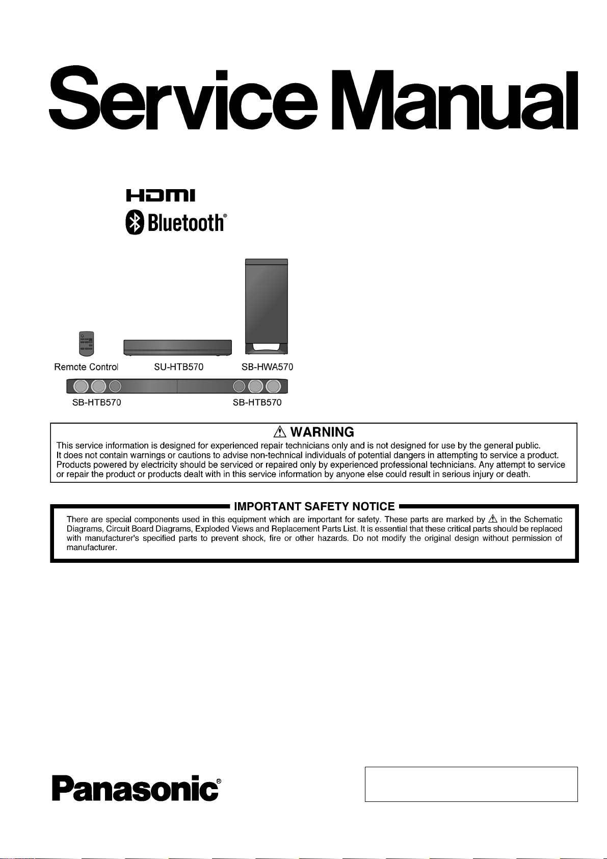
PANASONIC SU-HTB570EB, SU-HTB570EG, SB-HTB570EG, SB-HWA570EB, SB-HWA570EG Service Manual
...Page 1
PSG1302015CE
Home Theater Audio System
Model No. SU-HTB570EB
SU-HTB570EG
SB-HTB570EG
SB-HWA570EB
SB-HWA570EG
SC-HTB570EB
SC-HTB570EG
TABLE OF CONTENTS
1 Safety Precautions----------------------------------------------- 3
1.1. General Guidelines---------------------------------------- 3
1.2. Before Repair and Adjustment------------------------- 4
1.3. Protection Circuitry---------------------------------------- 4
1.4. Caution For Fuse Replacement------------------------ 4
1.5. Caution for AC Mains Plug (For EB only) ----------- 5
1.6. Safety Part Information----------------------------------- 6
1.7. Safety Installation Instructions ------------------------- 8
2 Warning-------------------------------------------------------------- 9
2.1. Prevention of Electrostatic Discharge (ESD)
to Electrostatically Sensitive (ES) Devices---------- 9
Product Color: (S)...Silver Type
PAGE PAGE
2.2. Service caution based on Legal restrictions
(Lead Free Solder, (PbF))------------------------------10
3 Service Navigation --------------------------------------------- 11
3.1. Service Information-------------------------------------- 11
4 Specifications----------------------------------------------------12
5 General/Introduction------------------------------------------- 13
5.1. About Bluetooth and Operation----------------------- 13
5.2. About VIERA Link---------------------------------------- 14
5.3. Others (Licenses)---------------------------------------- 15
6 Location of Controls and Components------------------16
6.1. Main Unit & Active Subwoofer Key Button
Operations------------------------------------------------- 16
© Panasonic Corporation 2013. All rights reserved.
Unauthorized copying and distribution is a violation of
law.
Page 2

6.2. Indicator illumination-------------------------------------18
6.3. Remote Control Key Button Operations------------19
7 Installation Instructions---------------------------------------20
7.1. Connections -----------------------------------------------20
8 Service Mode-----------------------------------------------------23
8.1. Method to enter into Service Mode------------------23
8.2. Model Display Details by LED Blinking
Indicators---------------------------------------------------23
8.3. Error Codes Display-------------------------------------26
8.4. Cold start (For SU-HTB570)---------------------------28
8.5. Pairing mode between Main Unit (SU) with
Active Subwoofer (SB-HWA)--------------------------28
8.6. SET AUDIO DELAY -------------------------------------28
9 Troubleshooting Guide----------------------------------------29
10 Service Fixture & Tools ---------------------------------------31
11 Disassembly and Assembly Instructions--------------- 32
11.1. Disassembly flow chart ---------------------------------33
1 1 .2. Types of Screws-------------------------------- ---------- 35
1 1 .3. Main Parts Location Diagram -------------------------36
11.4. Disassembly of Main Unit (SU-HTB570) ----------38
11.5. Disassembly of Front Speaker Units Position ----50
11.6. Disassembly of Front Speaker (L&R) (SBHTB570) --------------------------------------------------- 55
11.7. Disassembly of Active Subwoofer (SBHWA570)---------------------------------------------------74
12 Service Position -------------------------------------------------87
12.1. Main Unit (SU-HTB570) --------------------------------87
12.2. Active Subwoofer (SB-HWA570)---------------------92
13 Overall Simplified Block--------------------------------------95
13.1. Main Unit (SU-HTB570) --------------------------------95
13.2. Active Subwoofer (SB-HWA570)---------------------97
14 Block Diagram ---------------------------------------------------98
14.1. Main Unit (SU-HTB570) --------------------------------98
14.2. Active Subwoofer (SB-HWA570)------------------- 104
15 Wiring Connection Diagram------------------------------- 106
15.1. Main Unit (SU-HTB570) ------------------------------ 106
15.2. Active Subwoofer (SB-HWA570)------------------- 107
16 Schematic Diagram------------------------------------------- 109
16.1. Schematic Diagram Notes--------------------------- 109
16.2. Main Unit (SU-HTB570) -------------------------------11 1
16.3. Active Subwoofer (SB-HWA570)------------------- 122
17 Printed Circuit Board ---------------------------------------- 126
17.1. Main Unit (SU-HTB570) ----------------------------- 126
17.2. Active Subwoofer (SB-HWA570) ------------------ 131
18 Appendix Information of Schematic Diagram ------- 133
18.1. Voltage Measurement & Waveform Chart ------- 133
18.2. Illustration of IC’s, Transistors and Diodes ------ 141
18.3. Terminal Function of IC’s----------------------------- 143
19 Exploded View and Replacement Parts List--------- 145
19.1. Exploded View and Mechanical replacement
Parts List ------------------------------------------------- 145
19.2. Electrical Replacement Parts List------------------ 153
2
Page 3
1 Safety Precautions
1.1. General Guidelines
1. IMPORTANT SAFETY NOTICE
There are special components used in this equipment which are important for safety. These parts are marked by in the
Schematic Diagrams, Circuit Board Layout, Exploded Views and Replacement Parts List. It is essential that these critical parts
should be replaced with manufacturer’s specified parts to prevent X-RADIATION, shock, fire, or other hazards. Do not modify
the original design without permission of manufacturer.
2. An Isolation Transformer should always be used during the servicing of AC Adaptor whose chassis is not isolated from the AC
power line. Use a transformer of adequate power rating as this protects the technician from accidents resulting in personal
injury from electrical shocks. It will also protect AC Adaptor from being damaged by accidental shorting that may occur during
servicing.
3. When servicing, observe the original lead dress. If a short circuit is found, re place all parts which have been overheated or
damaged by the short circuit.
4. After servicing, see to it that all the protective devices such as insulation barriers, insulation papers shields are properly
installed.
5. After servicing, make the following leakage current checks to prevent the customer from being exposed to shock hazards.
1.1.1. Leakage Current Cold Check
1. Unplug the AC cord and connect a jumper between the two prongs on the plug.
2. Using an ohmmeter measure the resistance value, between the jumpered AC plug and each exposed metallic cabinet part on
the equipment such as screwheads, connectors, control shafts, etc. When the exposed metallic part has a return path to th e
chassis, the reading should be between 1MΩ and 5.2Ω. When the exposed metal does not have a return path to the chassis,
the reading must be
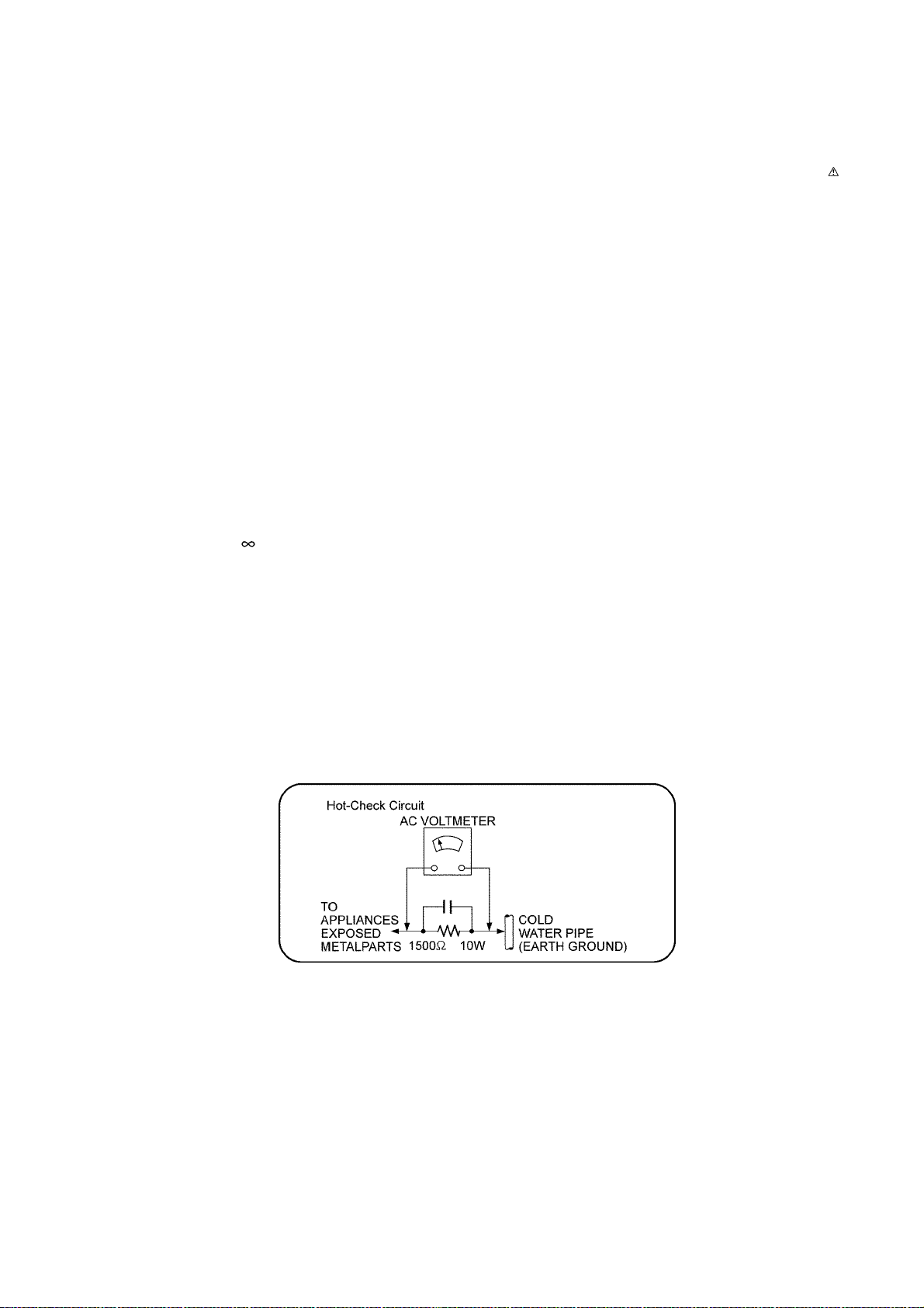
1.1.2. Leakage Current Hot Check
1. Plug the AC cord directly into the AC outlet. Do not use an isolation transformer for this check.
2. Connect a 1.5kΩ, 10 watts resistor, in parallel with a 0.15μF capacitors, between each exposed metallic part on the set and a
good earth ground such as a water pipe, as shown in Figure 1-1.
3. Use an AC voltmeter, with 1000 ohms/volt or more sensitivity, to measure the potential across the resistor.
4. Check each exposed metallic part, and measure the voltage at each point.
5. Reverse the AC plug in the AC outlet and repeat each of the above measurements.
6. The potential at any point should not exceed 0.75 volts RMS. A leakage current tester (Simpson Model 229 or e quivalent)
may be used to make the hot checks, leakage current must not exceed 1/2 milliamp. should the measurement is outside of
the limits specified, there is a possibility of a shock hazard, and the equipment should be repaired and re-checked before it is
returned to the customer.
Figure 1-1
3
Page 4
1.2. Before Repair and Adjustment
Main Unit (SU-HTB570)
Disconnect AC power, discharge unit AC Capacitors (C5700, C5701, C5702, C5703, C5704 and C5705) through a 10W, 1W resistor to ground.
Caution : DO NOT SHORT-CIRCUIT DIRECTLY (with a screwdriver blade, for instance), as this may destroy solid state devices.
After repairs are completed, restore power gradually using a variac, to avoid overcurrent.
• Current consumption at AC 220 V ~ 240 V, 50 Hz during power on at no signal with volume minimum, (Selector : CD mode)
should be ~150 mA.
Active Subwoofer (SB-HWA570)
Disconnect AC power, discharge unit AC Capacitors (C5700, C5701, C5702, C5703, C5704 and C5705) through a 10W, 1W resistor to ground.
Caution : DO NOT SHORT-CIRCUIT DIRECTLY (with a screwdriver blade, for instance), as this may destroy solid state devices.
After repairs are completed, restore power gradually using a variac, to avoid overcurrent.
• Current consumption at AC 220 V ~ 240 V, 60 Hz during power on at link with volume minimum, (Selector : BD/DVD mode)
should be ~200 mA.
1.3. Protection Circuitry
The protection circuitry may have operated if either of the following conditions are noticed:
• No sound is heard when the power is turned on.
• Sound stops during a performance.
The function of this circuitry is to prevent circuitry damage if, for example, the positive and negative speaker connection wir es are
"shorted", or if speaker systems with an impedance less than the indicated rated impedance of the amplifier are used.
If this occurs, follow the procedure outlines below:
1. Turn off the power.
2. Determine the cause of the problem and correct it.
3. Turn on the power once again after one minute.
Note:
When the protection circuitry functions, the unit will not operate unless the power is first turned off and then on again.
1.4. Caution For Fuse Replacement
1.4.1. SU-HTB570/SB-HWA570
Figure 1-2
4
Page 5
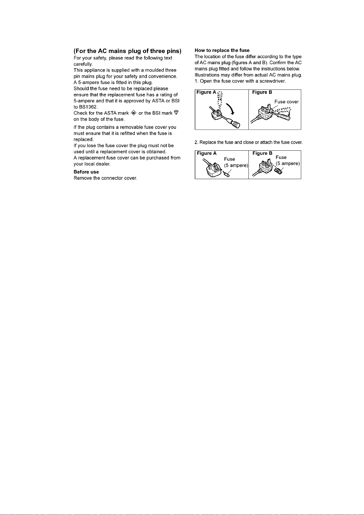
1.5. Caution for AC Mains Plug (For EB only)
Figure 1-3
5
Page 6
1.6. Safety Part Information
Safety Parts List:
There are special components used in this equipment which are important for safety.
These parts are marked by in the Schematic Diagrams & Replacement Parts List. It is essential that thes e critical p art s should
be replaced with manufacturer’s specified parts to prevent shock, fire or other hazards. Do not modify the original design without
permission of manufacturer.
1.6.1. Main Unit (SU-HTB570)
Safety Ref. No. Part No. Part Name & Description Remarks
3 REX1579 1P RED WIRE (SMPS-AC INLET)
4 REX1580 1P BLACK WIRE (SMPS-AC INLET)
16 RKM0662B-S TOP PANEL
18 RGR0441C-B REAR PANEL EG
18 RGR0441C-F REAR PANEL EB
29 RMZ1268 SMPS TOP INSULATOR
C5700 F1BAF1020020 1000pF
C5701 F0CAF104A105 0.1uF
C5702 F0CAF104A105 0.1uF
C5703 F0CAF104A105 0.1uF
C5704 F1BAF471A013 470pF
C5705 F1BAF471A013 470pF
DZ5701 ERZV10V511CS ZNR (E.S.D)
F1 K5G312Y00007 FUSE
L5702 G0B922G00004 LINE FILTER
L5703 G0B922G00004 LINE FILTER
P5701 K2AA2B000011 AC INLET
PC5720 B3PBA0000579 PHOTO COUPLER
PC5760 B3PBA0000579 PHOTO COUPLER
PCB4 REP4860G SMPS P.C.B (RTL)
PCB5 REP4860G AC INLET P.C.B. (RTL)
PCB6 REP4864A DIGITAL TRANSMISTTER MODULE P.C.B.
PCB7 N5HZZ0000128 BLUETOOTH MODULE P.C.B.
R5700 ERJ8GEYJ105V 1M 1/4W
R5701 ERJ8GEYJ105V 1M 1/4W
R5710 ERJ8GEYJ105V 1M 1/4W
T5701 ETS35BL196AD TRANSFORMER
1.6.2. Front Speaker (SB-HTB570)
Safety Ref. No. Part No. Part Name & Description Remarks
43 RGN3322-K SPEC LABEL
6
Page 7
1.6.3. Active Subwoofer (SB-HWA570)
Safety Ref. No. Part No. Part Name & Description Remarks
67 RGN3351-S1 NAME PLATE EG
67 RGN3352-S NAME PLATE EB
75 RMZX0026-1 IC INSULATOR
80 REX1579 1P RED WIRE (SMPS - AC INLET)
84 REX1580 1P BLACK WIRE (SMPS - AC INLET)
C5700 F1BAF1020020 1000pF
C5701 F0CAF104A105 0.1uF
C5702 F0CAF104A105 0.1uF
C5703 F0CAF104A105 0.1uF
C5704 F1BAF471A013 470pF
C5705 F1BAF471A013 470pF
DZ5701 ERZV10V511CS ZNR (E.S.D)
F1 K5G312Y00007 FUSE
L5702 G0B922G00004 LINE FILTER
L5703 G0B922G00004 LINE FILTER
P5701 K2AA2B000011 AC INLET
PC5720 B3PBA0000579 PHOTO COUPLER
PC5760 B3PBA0000579 PHOTO COUPLER
PCB4 REP4860L SW SMPS P.C.B. (RTL)
PCB5 REP4860L SW AC INLET P.C.B. (RTL)
R5700 ERJ8GEYJ105V 1M 1/4W
R5701 ERJ8GEYJ105V 1M 1/4W
R5710 ERJ8GEYJ105V 1M 1/4W
T5701 G4DYA0000485 TRANSFORMER
1.6.4. System (SC-HTB570)
Safety Ref. No. Part No. Part Name & Description Remarks
A1 N2QAYC000083 REMOTE CONTROL
A2 K2CT2YY00097 AC CORD EB
A2 K2CQ2YY00119 AC CORD EG
A3 RQT9781-D O/I BOOK (Fi/Ru/Ur) EG
A3 RQT9782-D O/I BOOK (Fr/It/Ge) EG
A3 RQT9783-E O/I BOOK (Sp/Po/Cz) EG
A3 RQT9784-H O/I BOOK (Sw/Da/Du) EG
A3 RQT9785-B O/I BOOK (En)
7
Page 8
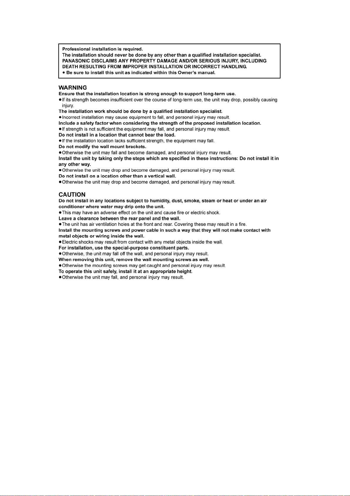
1.7. Safety Installation Instructions
Figure 1-4
8
Page 9
2Warning
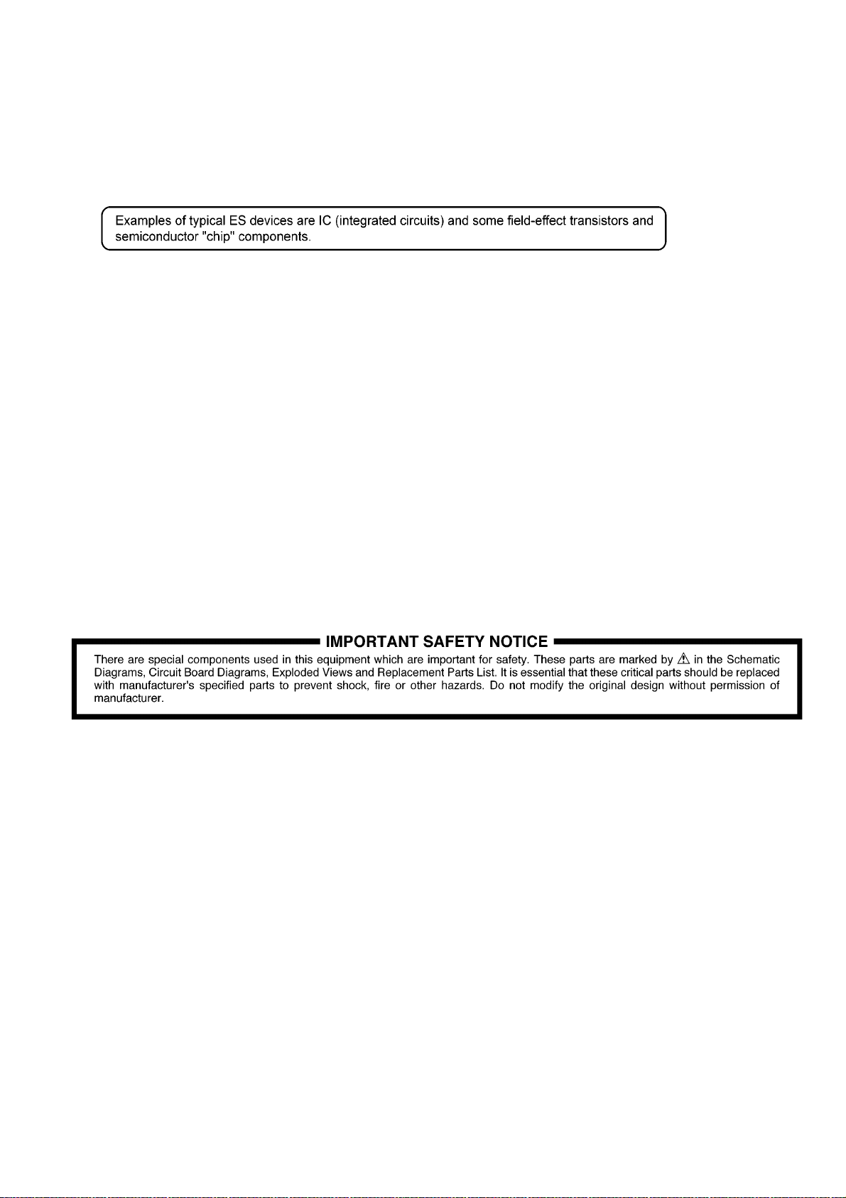
2.1. Prevention of Electrostatic Discharge (ESD) to Electrostatically Sensitive (ES) Devices
Some semiconductor (solid state) devices can be damaged easily by static electricity. Such components commonly are called Electrostatically Sensitive (ES) Devices.
The following techniques should be used to help reduce the incidence of compon ent damage caused by electrostatic discharge
(ESD).
1. Immediately before handling any semiconductor component or semiconductor-equipped assembly, drain off any ESD on your
body by touching a known earth ground. Alternatively, obtain and wear a commercially available discharging ESD wrist strap,
which should be removed for potential shock reasons prior to applying power to the unit under test.
2. After removing an electrical assembly equipped with ES devices, place the assembly on a condu ctive surface such as al uminum foil, to prevent electrostatic charge buildup or exposure of the assembly.
3. Use only a grounded-tip soldering iron to solder or unsolder ES devices.
4. Use only an anti-static solder removal device. Some solder removal devices not classified as “anti-static (ESD protected)” can
generate electrical charge sufficient to damage ES devices.
5. Do not use freon-propelled chemicals. These can generate electrical charges sufficient to damage ES devices.
6. Do not remove a replacement ES device from its protective package until immediately before you are ready to install it. (Most
replacement ES devices are packaged with leads electrically shorted together by conductive foam, aluminum foil or comparable conductive material).
7. Immediately before removing the protective material from the leads of a replacement ES device, touch the protective material
to the chassis or circuit assembly into which the device will be installed.
CAUTION:
Be sure no power is applied to the chassis or circuit, and observe all other safety precautions.
8. Minimize bodily motions when handling unpackaged replacement ES devices. (Otherwise harmless motion such as the
brushing together of your clothes fabric or the lifting of your foot from a carpeted floor can generate static electricity (ESD) sufficient to damage an ES device).
9
Page 10

2.2. Service caution based on Legal restrictions (Lead Free Solder, (PbF))
The lead free solder has been used in the mounting process of all electrical comp onents on the printed circuit boards us ed for this
equipment in considering the globally environmental conservation.
The normal solder is the alloy of tin (Sn) and lead (Pb). On the other hand, the lead free solder is the alloy mainly consists of tin
(Sn), silver (Ag) and Copper (Cu), and the melting point of the lead free solder is higher approx.30 degrees C (86°F) more than that
of the normal solder.
Definition of PCB Lead Free Solder being used
The letter of “PbF” is printed either foil side or components side on the PCB using the lead free solder.
(See right figure)
Service caution for repair work using Lead Free Solder (PbF)
• The lead free solder has to be used when repairing the equipment for which the lead free solder is used.
(Definition: The letter of “PbF” is printed on the PCB using the lead free solder.)
• To put lead free solder, it should be well molten and mixed with the original lead free solder.
• Remove the remaining lead free solder on the PCB cleanly for soldering of the new IC.
• Since the melting point of the lead free solder i s higher than that of the normal lead solder, it takes the longer time to melt the
lead free solder.
• Use the soldering iron (more than 70W) e quipped with the tempe rature control after setting the te mperature at 350±30 degrees
C (662±86°F).
Recommended Lead Free Solder (Service Parts Route.)
• The following 3 types of lead free solder are available through the service parts route.
RFKZ03D01K-----------(0.3mm 100g Reel)
RFKZ06D01K-----------(0.6mm 100g Reel)
RFKZ10D01K-----------(1.0mm 100g Reel)
Note
* Ingredient: Tin (Sn), 96.5%, Silver (Ag) 3.0%, Copper (Cu) 0.5%, Cobalt (Co) / Germanium (Ge) 0.1 to 0.3%
10
Page 11

3 Service Navigation
3.1. Service Information
This service manual contains technical information which will allow service personnel’s to understand and service this model.
Please place orders using the parts list and not the drawing reference numbers.
If the circuit is changed or modified, this information wil l be fol lowed by supp lement service ma nual to be filed with original servic e
manual.
• Flash IC :
The following components are supplied as an assembled part.
• Flash IC, IC2001 (RFKWEHTB370M).
11
Page 12

4 Specifications
Q Amplifier Section
RMS Output Power : Dolby Digital Mode
Front ch (L, R ch) 60 W per channel (6 Ω), 1 kHz,
10% THD
Subwoofer ch 120 W per channel (8 Ω), 100 Hz,
10% THD
Total RMS Dolby Digital mode
power
Q Wireless section
Wireless module
Frequency Range 2.40335 GHz to 2.47735 GHz
Number of channels 38
Q Terminal Section
HDAVI Control This unit supports “HDAVI Control
HDMI AV input (BD/DVD) 1
Input connector Type A (19 pin)
HDMI AV output (TV (ARC)) 1
Output connector Type A (19 pin)
Digital audio input
Optical digital input (TV, AUX) 2
Sampling frequency 32 kHz, 44.1 kHz, 48 kHz
88.2 kHz, 96 kHz (only LPCM)
Audio format LPCM, Dolby Digital, DTS Digital
IR Blaster
Terminal Type 3.5 mm jack
USB Port For service use only.
Q Speaker Section
Front speakers
3 way, 3 speaker system (Bass reflex type)
Speaker unit(s) Impedance 6 Ω
Woofer 5.7 cm cone type
Tweeter 2.5 cm semi-dome type
Super tweeter Piezo type
Output sound pressure 78 dB/W (1 m)
Frequency range 90 Hz to 32 kHz (-16 dB)
100 Hz to 23 kHz (-10 dB)
Active subwoofer
1 way, 1 speaker system (Bass reflex type)
Woofer 16 cm cone type
Output sound pressure 80 dB/W (1 m)
Frequency range 30 Hz to 180 Hz (-16 dB)
35 Hz to 160 Hz (-10 dB)
Q General
Power consumption Main Unit: 27 W
Active subwoofer: 19 W
In standby condition
Main Unit (When the other connected devices are turned off):
Active subwoofer (Power switch release):
Approx. 0.25 W
Power supply AC 220 V to 240 V, 50 Hz
Dimensions (W x H x D)
Main Unit
310 mm x 45 mm x 188 mm
Active subwoofer 180 mm x 408 mm x 306 mm
Mass (Weight)
Main Unit Approx. 1.15 kg
Active subwoofer 4.76 kg
Operating temperature range 0°C to +40°C
240 W
5” function.
Surround
Approx. 0.3 W
Operating humidity range 20% to 80 % RH
(no condensation)
Q Speaker General
- For wall mounting layout
Horizontal placement
Dimensions (W x H x D) 1060 mm x 68 mm x 41 mm
Mass (Weight)
Vertical placement
Dimensions (W x H x D) 68 mm x 541 mm x 41 mm
Mass (Weight) 0.78 kg
- For table top layout
Horizontal placement using the leg stands (High)
Dimensions (W x H x D) 1060 mm x 96 mm x 68 mm
Mass (Weight) 1.57 kg
Horizontal placement using the leg stands (Low)
Dimensions (W x H x D) 1060 mm x 87 mm x 68 mm
Mass (Weight) 1.57 kg
Horizontal placement using the support legs and the speaker feet
Dimensions (W x H x D) 1060 mm x 71 mm x 60 mm
Mass (Weight) 1.53 kg
Vertical placement using the bases
Dimensions (W x H x D) 148 mm x 552 mm x 148 mm
Mass (Weight) 0.89 kg
Center Speaker
Q Bluetooth Section
Bluetooth system specification Version 3.0
Wireless equipment classification
Supported profiles A2DP
Frequency band 2402 MHz to 2480 MHz
(Adaptive Frequency Hopping)
Operating distance 10 m Line of Sight
• Specifications are subject to change without notice. Weight and
dimensions are approximate.
• Total harmonic distortion is measured by the digital spectrum analyzer.
Q System: SC-HTB570EBS MAIN UNIT : SU-HTB570EBS
FRONT SPEAKERS : SB-HTB570EGS
ACTIVE SUBWOOFER : SB-HWA570EBS
Q System: SC-HTB570EGS MAIN UNIT : SU-HTB570EGS
FRONT SPEAKERS : SB-HTB570EGS
ACTIVE SUBWOOFER : SB-HWA570EGS
1.49 kg
Class 2
12
Page 13
5 General/Introduction
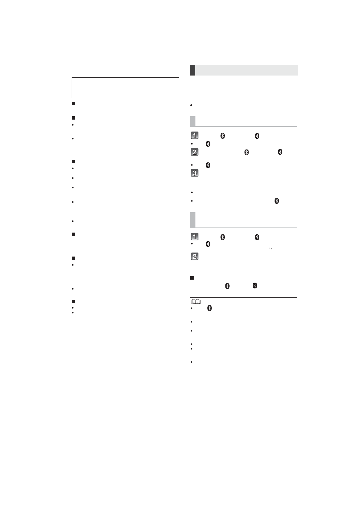
By using the Bluetooth®connection, you can listen
to the sound from the Bluetooth
®
audio device
from this system wirelessly.
Preparation
Turn on the Bluetooth®feature of the device and
place the device near the main unit.
Press [ ] to select “ ”.
If the “ ” indicator flashes quickly, go to step 3.
Press and hold [ ] until the “ ”
indicator flashes quickly.
If the “ ” indicator flashes slowly, repeat step 2.
Select “SC-HTB570” from the
Bluetooth
®
device’s Bluetooth
®
menu.
If prompted for the passkey on the Bluetooth® device, enter
“0000”.
Once the Bluetooth
®
device is connected, the “ ” indicator
stops flashing and lights up.
Press [ ] to select “ ”.
If the “ ” indicator lights, a Bluetooth® device is already
connected with this system. Disconnect it. (
below)
Select “SC-HTB570” from the
Bluetooth
®
device’s Bluetooth
®
menu.
Disconnecting a Bluetooth
®
device
Press and hold [ ] until the “ ” indicator flashes
slowly.
When “ ” is selected as the source, this system will
automatically try and connect to the last connected
Bluetooth
®
device.
The Bluetooth
®
device will be disconnected if a different
audio source (e.g. “TV“) is selected.
Refer to the operating instructions of the Bluetooth
®
device
for further instruction on how to connect a Bluetooth
®
device.
This system can only be connected to one device at a time.
You can register up to 8 devices with this system. If a 9th
device is paired, the device that has not been used for the
longest time will be replaced.
To change the sound quality, refer to OI Book “Bluetooth
®
communication mode”.
Bluetooth®connection
Bluetooth® pairing
Connecting a Bluetooth
®
device
About Bluetooth
®
Frequency band used
This system uses the 2.4 GHz frequency band.
Certification of this device
This system conforms to frequency restrictions and has
received certification based on frequency laws. Thus, a
wireless permit is not necessary.
The action below are punishable by law in some
countries:
Taking apart or modifying the unit.
Removing specification indications.
Restrictions of use
Wireless transmission and/or usage with all Bluetooth
®
equipped devices is not guaranteed.
All devices must conform to standards set by Bluetooth
SIG, Inc.
Depending on the specifications and settings of a
device, it can fail to connect or some operations can be
different.
This system supports Bluetooth
®
security features. But
depending on the operating environment and/or
settings, this security is possibly not sufficient. Transmit
data wirelessly to this system with caution.
This system cannot transmit data to a Bluetooth
®
device.
Range of use
Use this device at a maximum range of 10 m.
The range can decrease depending on the environment,
obstacles or interference.
Interference from other devices
This system may not function properly and troubles
such as noise and sound jumps may arise due t
o radio
wave interference if the main unit is located too close to
other Bluetooth
®
devices or the devices that use the 2.4
GHz band.
This system may not function properly if radio waves
from a nearby broadcasting station, etc. are too strong.
Intended usage
This system is for normal, general use only.
Do not use this system near equipment or in an
environment that is sensitive to radio frequency
interference (example: airports, hospitals, laboratories,
etc).
Panasonic bears no responsibility for data
and/or information that is compromised
during a wireless transmission.
-
-
5.1. About Bluetooth and Operation
13
Page 14

5.2. About VIERA Link
Linked operations with the TV
(VIERA Link
TM
“HDAVI ControlTM”)
Preparation
1 Confirm that the HDMI connection has been made.
2 Set the “HDAVI Control” operations on the connected
equipment (e.g., TV).
3 For the optimal “HDAVI Control” operations change
the following settings on the connected TV
1
.
Set the default speaker settings to this system.
2
Set the speaker selection settings to this system.
4 Turn on all “HDAVI Control” compatible equipment
and select the TV’s input for this system so that the
“HDAVI Control” function works properly.
5 If a device is connected to the HDMI IN t
erminal, start
play to check that the picture is displayed on the TV
correctly.
When the connection or settings are changed,
repeat this procedure.
1 The availability and function of the settings may vary
depending on the TV. Refer to the operating instructions
for the TV for details.
2 If the TV has a default speaker setting within the VIERA
Link setting items, choosing this system as the default
speaker will automatically change the speaker selection to
this system.
VIERA Link “HDAVI Control”, based on the control functions
provided by HDMI which is an industry standard known as
HDMI CEC (Consumer Electronics Control), is a unique
function that we have developed and added. As such, its
operation with other manufacturers’ equipment that
supports HDMI CEC cannot be guaranteed.
This unit supports “HDAVI Control 5” function.
“HDAVI Control 5” is the standard for Panasonic’s HDAVI
Control compatible equipment. This standard is compatible
with Panasonic’s conventional HDAVI equipment.
Please refer to individual manuals for other manufacturers’
equipment supporting VIERA Link function.
To make sure that the audio is output from this system,
turn the main unit on by using the TV’s remote control and
selecting home theater from the speaker menu of VIERA
Link menu. The availability and function of the settings
may vary depending on the TV. Refer to the operating
instructions for the TV for details.
Speaker control
You can select whether audio output is from this system or
the TV
speakers by using the TV menu settings.
Home theater
This system is active.
When the main unit is in standby mode, changing the TV
speakers to this system in the VIERA Link menu will
automatically turn the main unit on and select TV as the
source.
You can control the volume setting of this system using the
volume or mute button on the TV remote control.
If you turn off the main unit, the TV speakers will be
automatically activated.
Audio will automatically be output from this system if the TV
is compatible to VIERA Link “HDAVI Control 4” or later.
TV
TV speakers are active.
The volume of this system is set to its minimum.
Automatic input switching
When the following operations are performed, the main
unit will automatically change the input to the
corresponding source.
When play starts on an HDMI connected device.
3
When the TV input or the TV channel is changed.
3 If the speaker output setting on the TV is set to this
system, the TV and the main unit turn on automatically
(Power on link).
Power off link
When the TV is turned off, the main unit also turns off
automatically. (This function does not work when
Bluetooth
®
is the source.)
Automatic lip-sync function
(for HDAVI Control 3 or later)
Delay between audio and video is automatically adjusted
by adding time-lag to the audio output, enabling you to
enjoy smooth audio for the picture.
The delay information is automatically set if the TV is
compatible to VIERA Link “HDAVI Control 3” or later and the
VIERA Link is set to on.
What is VIERA Link “HDAVI
Control”?
VIERA LinkTM is a new name for EZ SyncTM.
VIERA Link “HDAVI Control” is a convenient
function that offers linked operations of this
system, and a Panasonic TV (VIERA) under
“HDAVI Control”.
You can use this function by connecting the
equipment with an HDMI cable. See the
operating instructions for connected
equipment for operational details.
What you can do with
VIERA Link “HDAVI
Control”
-
-
14
Page 15

5.3. Others (Licenses)
Manufactured under license from Dolby Laboratories.
Dolby, Pro Logic, and the double-D symbol are trademarks
of Dolby Laboratories.
Manufactured under license under U.S. Patent Nos:
5,956,674; 5,974,380; 6,487,535 & other U.S. and
worldwide patents issued & pending.
DTS, the Symbol, & DTS and the Symbol together are
registered trademarks & DTS Digital Surround and the DTS
logos are trademarks of DTS, Inc. Product includes
software.
© DTS, Inc. All Rights Reserved.
HDMI, the HDMI Logo, and High-Definition Multimedia
Interface are trademarks or registered trademarks of HDMI
Licensing LLC in the United States and other countries.
HDAVI Control™ is a trademark of Panasonic Corporation.
The Bluetooth
®
word mark and logos are owned by the
Bluetooth SIG, Inc. and any use of such marks by
Panasonic Corporation is under license. Other trademarks
and trade names are those of their respective owners.
15
Page 16

6 Location of Controls and Components
A
B
C
D
E
F
1
Press to switch the unit from on to standby
mode or vice versa. In standby mode, the unit
is still consuming a small amount of power.
2 Adjust the volume of this system
3 Select the input source
“TV” “BD/DVD” “AUX”
“”
4 Input selector indicators*
1
Bluetooth®indicator
Lights blue when the Bluetooth
®
device is
the audio source
TV indicator
Lights green when the TV is the audio
source
BD/DVD indicator
Lights amber when the device connected
to the BD/DVD terminal is the audio
source
AUX indicator
Lights amber when the device connected
to the AUX terminal is the audio source
5 Sound mode indicators*
1
STANDARD indicator
Lights when STANDARD is the current
sound mode
STADIUM indicator*
2
Lights when STADIUM is the current
sound mode
MUSIC indicator*
2
Lights when MUSIC is the current sound
mode
CINEMA indicator
Lights when CINEMA is the current
sound mode
NEWS indicator
Lights when NEWS is the current sound
mode
STEREO indicator
Lights when STEREO is the current
sound mode
6 Remote control signal sensor
7 WIRELESS LINK indicator
*1
The indicators will also blink in various conditions.
*2
The indicator blinks for 5 sec when the main unit detects an audio format.
To manually verify the current audio format and the corresponding indicators,
refer to O/I Book on
(Audio format indicator).
7
654
1
2
3
Main unit
Active subwoofer
This system (Front)
Standby/on switch ( /I)
G
H
I
J
6.1. Main Unit & Active Subwoofer Key Button Operations
6.1.1. Front View
16
Page 17

6.1.2. Rear View
1 AC IN terminal
2 Speaker terminals
3 OPTICAL DIGITAL AUDIO IN (TV) terminal
4 OPTICAL DIGITAL AUDIO IN (AUX) terminal
5 USB port (for service use only)
6 HDMI IN terminal
7 HDMI OUT terminal (ARC compatible)
8 Active subwoofer on/off button
* The I/D SET button is only used when the main unit is not paired with the active subwoofer.
*
AV OUT
TV(ARC)
AV IN
BD/DVD
AV OUT
TV(ARC)
AV IN
BD/DVD
This system (Rear)
17
Page 18

6.2. Indicator illumination
noitpircseDrotacidnI
The indicators display the condition of this system by flashing. The indicator patterns illustrated below
are displayed during normal operational conditions. They do not refer to the indications of a problem.
*1
The indicator for the current status remains lit.
*2
The BD/DVD indicator stops blinking and lights once the wireless pairing is successful.
*3
The indicator blinks only when [SOUND] is pressed for more than 4 sec and the audio format is PCM.
The BD/DVD indicator blinks*2and sound mode
indicators light up in sequence for 1 minute.
When the main unit is in wireless pairing mode with
the active subwoofer
The indicator blinks for 10 sec.
When the Bluetooth®communication is mode 1
The indicator blinks for 20 sec.
When 3D surround effect and clear-mode dialog
effect are on
When the dual audio setting is Main
When the auto gain control is on
When the auto standby function is on
The indicator blink
sfor5sec.
When the audio format is Dolby Digital
The indicator blinks for 5 sec.
When the audio format is DTS
The indicator blinks for 5 sec.
When the audio format is PCM*
3
The indicator blinks for 10 sec.
When the Bluetooth®communication is mode 2
The indicator blinks for 20 sec.
When 3D surround effect and clear-mode dialog
effect are off
When the dual audio setting is Secondary
(SAP: Secondary Audio Program)
When the auto gain control is o
ff
When the auto standby function is off
The indicators blink for 20 sec.
When the dual audio setting is Main and Secondary
The indicators blink for 10 sec.
When the remote control code is changed
The indicators blink once.
When changing the setting (“To reduce the clear-mode
dialog effect”, “To turn off VIERA Link “HDAVI Control””,
and “To turn off the volume limitation”)
The indicators blink twice.
When the main unit is reset
Bluetooth
®
indicator blinks quickly.
When the m
ain unit is ready for pairing
Bluetooth
®
indicator blinks slowly.
When the main unit is waiting to connect
Bluetooth
®
indicator turns on.
When the main unit is connected with a Bluetooth®device
*1
*1
*1
*1
18
Page 19
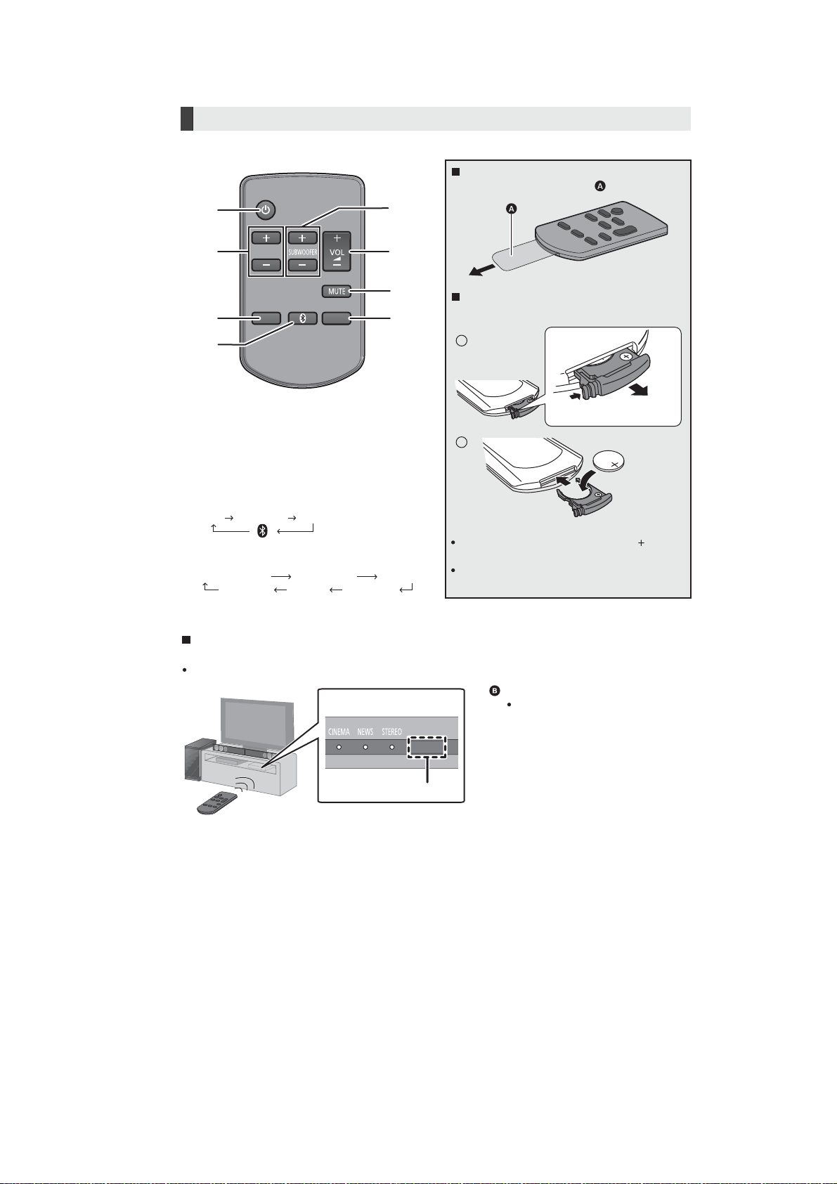
6.3. Remote Control Key Button Operations
“STANDARD” “STADIUM” “MUSIC”
“STEREO” “NEWS” “CINEMA”
1 Turn the main unit on or off
2 Adjust the dialog effect level
3 Adjust the output level of the active
subwoofer (bass sound)
4 Adjust the volume of this system
5 Mute the sound
6 Select the input source
“TV” “BD/DVD” “AUX”
“”
7 Select the Bluetooth
®
device as the source
8 Select the sound mode
Remote control operation range
The remote control signal sensor is located on the main unit.
Use the remote control within the correct operation range.
DIALOG LEVEL
LINK MODE
PAIRING
----
SOUND
1
6
7
2
3
4
5
8
INPUT
SELECTOR
Before using for the first time
Remove the insulation sheet .
To replace a button-type battery
Battery type: CR2025 (Lithium battery)
Set the button-type battery with its ( )mark
facing upward.
Keep the button-type battery out of reach of
children to prevent swallowing.
Remote control signal sensor
Operation range
Distance: Within approx. 7 m
directly in front
Angle: Approx. 30
o
left and right
Remote control
1
2
19
Page 20

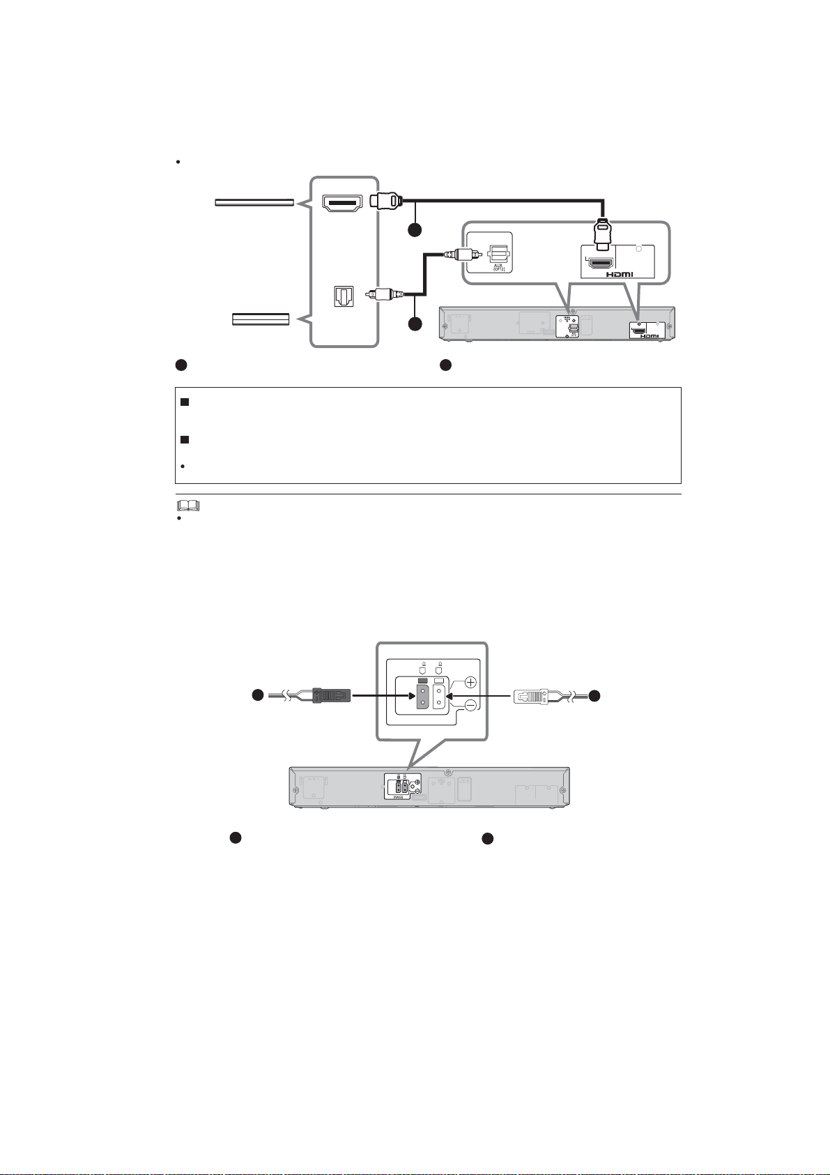
7 Installation Instructions
Turn off all equipment before connection and read the appropriate operating instructions.
Do not connect the AC mains lead until all other connections are completed.
HDMI
The HDMI connection supports VIERA Link “HDAVI Control” when used with a compatible Panasonic TV.
Use the ARC compatible High Speed HDMI cables. Non-HDMI-compliant cables cannot be utilized.
It is recommended that you use Panasonic’s HDMI cable.
B
Verify if the TV’s HDMI terminal is labeled “HDMI (ARC)”.
What is ARC?
ARC is an abbreviation of Audio Return Channel, also known as HDMI ARC. It refers to one of the HDMI functions. When you
connect the main unit to the terminal labeled “HDMI (ARC)” on the TV, the optical digital audio cable that is usually required in
order to listen to sound from a TV is no longer required, and TV pictures and sound can be enjoyed with a single HDMI cable.
Make the connection.
Connection differs depending on the label printed next to the HDMI terminal.
Labeled “HDMI (ARC)”: Connection
Not Labeled “HDMI (ARC)”: Connection
Labeled “HDMI (ARC)”
Not labeled “HDMI (ARC)”
A
Main unit
HDMI cable
A
AV OUT
TV(ARC)
HDMI IN (ARC)
AV OUT
TV(ARC)
Be sure to connect to the
TV’s ARC compatible
terminal. (Refer to the
operating instructions for
the TV.)
TV
A
B
A
HDMI cable
Optical digital audio cable
When you use the optical digital audio cable, insert the tip correctly into the terminal.
AV OUT
TV(ARC)
HDMI IN
OPTICAL
OUT
AV OUT
TV(ARC)
DIGITAL
AUDIO
IN
TV
(OPT1)
TV
B
A
7.1. Connections
7.1.1. Connection with the TV
20
Page 21
7.1.2. Connection with other devices
A B
You can direct the audio signal from the connected Blu-ray Disc player, DVD player, Set Top Box, etc. to
this system.
Preparation
Connect the main unit to the TV.
HDMI cable Optical digital audio cable
Refer to the operating instructions of the connected HDMI compatible device for the necessary setting, to output the video
and audio signals.
HDMI OUT
OPTICAL
OUT
AV IN
BD/DVD
AV IN
BD/DVD
DIGITAL
AUDIO
IN
e.g., Set top box
e.g., Blu-ray Disc player
HDMI standby pass-through
Even if the main unit is in standby mode, the audio and/or video signal from the device connected to the HDMI IN terminal will
be sent to the TV connected to the HDMI OUT terminal (the sound will not be output from this system).
3D compatibility
Compatible with FULL HD 3D TV and Blu-ray Disc player.
The main unit can pass-through the 3D video signal from a 3D compatible Blu-ray Disc player to a FULL HD 3D TV.
A
B
Main unit
Match the connector shape and connect to the terminals of the same colour.
A RED
Right speaker connector
B WHITE
Left speaker connector
A
B
A
B
7.1.3. Speaker cable connection
6 6
R
L
SPEAKERS
AV IN
AV OUT
TV(ARC)
BD/DVD
21
Page 22

7.1.4. AC mains lead connection
Active subwoofer
Connect only after all other connections are completed.
This system consumes a small amount of AC power even when it is turned off. In the interest
of power conservation, if you will not be using this system for a long time, unplug it from the household
mains socket.
To a household mains socket AC mains lead (supplied)
BE SU RE TO R EA D T HE CAUTION FOR T HE AC MAINS LEAD ON OI BOOK BEFOR E
CONNECTION.
Saving energy
The main unit is designed to conserve its power consumption and save energy.
The main unit will automatically switch to standby mode when no signal is input and no operation is
performed for approx. 2 hours. Refer to OI Book, “Auto standby function” to turn this function off.
AV OUT
TV(ARC)
AV IN
BD/DVD
D
C
C
DC
For customers in United Kingdom and Ireland
22
Page 23
8 Service Mode
This unit is equipped with features of self-d iagn ostic & spec ial mode setting for checking the functions & reliability of the
unit.
Special Note : Checking of the reliability (ageing) & operation must be carry out to ensure good working condition in unit.
8.1. Method to enter into Service Mode
Here are the procedures to enter into service mode:
Step 1 : Power up the unit.
Step 2 : Press & hold [VOL-] on the unit, follow by [SUB-] & [SUB+] on the remote control.
Note : All LEDs will blink 4 times followed b y all LEDs off.
Step 3 : It enters into service mode.
8.2. Model Display Details by LED Blinking Indicators
After entering into service mode, the following keys on the remote control can be pressed to determine:-
1. Microprocessor firmware version number
2. Model No.
3. Region setting
4. Wireless pairing
Note : The LED blinking process will stop when the unit is power off completely.
Table 8-1
23
Page 24

8.2.1. Firmware version
It is to indicate the firmware version no. (Refer to table 8-2 for more information).
The firmware version is represented by 5 bits.
Version number display are repeated every 64 releases.
Version No Bit 5 Bit 4 Bit 3 Bit 2 Bit 1 Bit 0
01, 65 … X X X X X O
02, 66 … X X X X O X
03, 67 … X X X X O O
04, 68 … X X X O X X
05, 69 … X X X O X O
06, 70 … X X X O O X
07, 71 … X X X O O O
08, 72 … X X O X X X
09, 73 … X X O X X O
10, 74 … X X O X O X
11, 75 … X X O X O O
12, 76 … X X O O X X
13, 77 … X X O O X O
14, 78 … X X O O O X
15, 79 … X X O O O O
16, 80 ... X O X X X X
17, 81 … X O X X X O
18, 82 … X O X X O X
19, 83 … X O X X O O
20, 84 … X O X O X X
21, 85 … X O X O X O
22, 86 … X O X O O X
23, 87 … X O X O O O
24, 88 … X O O X X X
25, 89 … X O O X X O
26, 90 … X O O X O X
27, 91 … X O O X O O
28, 92 … X O O O X X
29, 93 … X O O O X O
30, 94 … X O O O O X
31, 95 … X O O O O O
32, 96 ... O X X X X X
33, 97 … O X X X X O
34, 98 … O X X X O X
35, 99 … O X X X O O
36, 100 … O X X O X X
37, 101 … O X X O X O
38, 102 … O X X O O X
39, 103 … O X X O O O
40, 104 … O X O X X X
41, 105 … O X O X X O
42, 106 … O X O X O X
43, 107 … O X O X O O
44, 108 … O X O O X X
45, 109 … O X O O X O
46, 110 … O X O O O X
47, 111 … O X O O O O
48, 112 ... O O X X X X
49, 113 … O O X X X O
50, 114 … O O X X O X
51, 115 … O O X X O O
52, 116 … O O X O X X
53, 117 … O O X O X O
54, 118 … O O X O O X
55, 119 … O O X O O O
56, 120 … O O O X X X
57, 121 … O O O X X O
58, 122 … O O O X O X
59, 123 … O O O X O O
60, 124 … O O O O X X
61, 125 … O O O O X O
24
Page 25
Version No Bit 5 Bit 4 Bit 3 Bit 2 Bit 1 Bit 0
62, 126 … O O O O O X
63, 127 … O O O O O O
Link Status
“O” means LED on
“X” means LED off
Table 8-2
8.2.2. Model Number Display
It is to indicate the model number. (Refer to table 8-3 for more information).
Model 1 Model 2 Model 3 Model No.
X O O HTB770
O X X HTB570
O X O HTB370
O O X Reserve 1
OOOReserve 2
Link Status
“O” means LED on
“X” means LED off
Table 8-3
8.2.3. Region Bit No.
It is to indicate the region for the model number. (Refer to table 8-4 for more information).
REG2 REG1 REG0 Region
X X X Europe / Ocenia / Asia / South /
X O X US / Canada
X O O China
O X X Japan
O X O Reserve 1
O O X Reserve 2
OOOReserve 3
Link Status
“O” means LED on
“X” means LED off
Centr. America / China / Russia
Table 8-4
25
Page 26
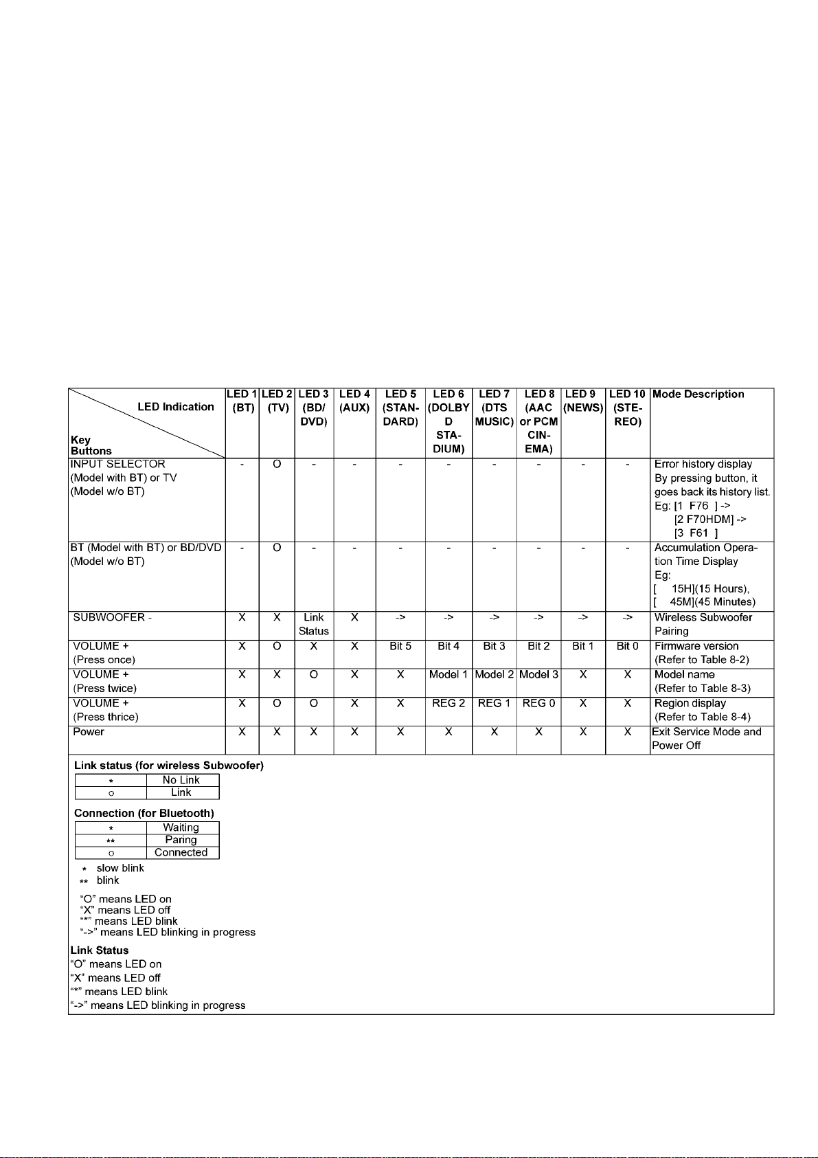
8.3. Error Codes Display
This unit does not have a FL/LCD display unit hence error code (w hen a fault condition occurs) is represented by the LED status
indicators. Refer to Figure 8-1
Here is the description of the LED status indicators:
Table 8-5
Figure 8-1
26
Page 27

8.3.1. Error Code Display Details by LED Blinking Indicators
This section describes the LED status indicators by its blinking to represent th e error codes.
Caution: The LED blinking process will stop only when the unit is power off completely .
Error Code LED 1
OVERLOAD (F61)
If this error occurs, main set
will automatically power off.
F76
If this error occurs, main set
will automatically power off.
F70 HDMI
F70 BT
U701 / U703 / U704
USB Update Fail
USB Overcurrent
“X” means LED off.
“*” means LED blink
(BT)
X**XXX X X XX
X*XXXX X X XX
X**XX* * * XX
***XXXX XXX
XX*XXX X X XX
XXXXXX X X X*
***X** * * **
LED 2
(TV)
LED 3
(BD/
DVD)
LED 4
(AUX)
LED 5
(STA
NDAR
D)
LED 6
(MUSIC/
(STADIUM/
DOLB
Y D)
Table 8-6
LED 7
DTS)
LED 8
(CIN-
EMA/
AAC or
PCM)
LED 9
(NEW
S)
LED 10
(STEREO)
Cause and Problem
Speaker protection, DAMP IC
abnormality. Check for faulty
parts and replace with new parts
if necessary.
DC Power/Voltage Supply abnormality. Check for faulty parts and
replace with new parts if necessary.
HDMI Micro-P to Main Micro-P IC
communication error. Check for
faulty parts and replace with new
parts if necessary.
Bluetooth communication error.
Check for faulty parts and replace
with new parts if necessary.
• Connected devices error
(HDCP non-compliance).
Check for faulty parts and
replace with new parts if necessary.
• HDMI connection abnormality
(cable damage, HDCP noncompliance etc). Check for
faulty parts and replace with
new parts if necessary.
• HDMI image format incompatibility. Check for faulty part s and
replace with new parts if necessary.
USB communication error. Check
for faulty parts and replace with
new parts if necessary.
USB communication error. Check
for faulty parts and replace with
new parts if necessary.
27
Page 28
8.4. Cold start (For SU-HTB570)
Step 1 : Power up the unit.
Step 2 : Press & hold [POWER] button on the unit for 4s or more.
All LED will light-up and blink for 2 times (at frequency of 4Hz)
Figure 8-2
8.5. Pairing mode between Main Unit (SU) with Active Subwoofer (SB-HWA)
Here are the procedures to do pairing between Main Unit (SU-HTB570) with Active Subwoofer (SB-HWA570)
Step 1 : Power up the Main Unit & Active Subwoofer.
Note : Please check the connections in Main Unit and Active Subwoofer when either fails to power up.
(WIRELESS LINK indicator on Active Subwoofer should turn RED if it is not linked)
Step 2 : Press [ID SET] on the rear of Active Subwoofer for more that 3 sec. (The WIRELESS LINK indicator will blink in red)
WIRELESS LINK indicator on Active Subwoofer shall blinking for up to 1 minutes to indicate it is in ready for pairing mode.
Step 3 : During WIRELESS LINK indicator on Active Subwoofer blinking, press [INPUT SELECTOR] or [AUX] on remote control followed by [VOL +] on Main Unit for more than 4 sec. (Pairing begins)
This step also can be carried out under Service Mode by press [SUB-] on remote control. (Pairing begins)
Note :
1. Under Pairing Mode, [BD/DVD] LED blinking and 6 indicators LEDs (STANDARD, STADIUM(Dolby D), MUSIC(DTS),
CINEMA(AAC/PCM), NEWS and STEREO) will run one by one (shifting) for every 1 sec from left to right to indicate it
is searching for the receiver to be linked and repeated the cycle after reached the [STEREO] LED.
2. When pairing is completed. [BD/DVD] LED on Main Unit will light up and WIRELESS LINK indicator on Active Sub-
woofer turns GREEN if pairing is successful.
3. Wireless pairing automatically exit after 1 minute.
Figure 8-3
8.6. SET AUDIO DELAY
If the video from TV late compared to audio output from this unit, this unit can be set the audio delay to 150ms fixed delay.
Step 1 : Power up the main unit.
Step 2 : Press & hold [VOL-] button on main unit and follow by [VOL-] and [SUB-] on remote control.
All LED will light-up and blink once for confirmation display and audio delay setting is set to 150ms.
28
Page 29
9 Troubleshooting Guide
䞉How to reset䚷䠄Factory setup condition䠅
䠍䠊Turn on the power of main set.
䠎䠊Press and hold the power button for 5 seconds.
(Repeat the flashing of all LED twice)
3䠊Turn off the power.
䞉The entering method of Service Mode䚷(after turn off the power, you can exit from Service Mode)
䠍䠊 Setting main set in power on status.
䠎䠊 Press the main set [Volume-] button, then continue press the [SUB -] & [SUB +] of remote control.
(All LEDs will blink four times, followed by all LEDs OFF)
SC-HTB570
Main set power ON Power do not turn on Power on by remote control ・OK
Power on by remote control ・NG
Check the connection of FFC connector
FFC wire checking
Switch operation checking
LED display checking
(The input display LED not lit)
Power input but turn off immediately
・Check the 13P of [Panel]-[Main] & 26P of [HDMI]-[Main] & 10P of [Switching power module]-[Main] & each FFC connector.
・Check the 13P of [Panel]-[Main] & 26P of [HDMI]-[Main] & 10P of [Switching power module]-[Main] & each FFC wire.
・7KHERWKHQGYROWDJHRI>3DQHO@SRZHUVZLWFK6LVSUHVVĺ09UHOHDVHĺ9
Check the connection of FFC connector ・wire
Checking the system 5V circuit
Checking the AC inlet code
Checking fuse cut
・&KHFN>3DQHO@&1ĺ9&1ĺ9))&FRQQHFWRURI3FRQQHFWLRQ
・[Switching power module] CN1(5)ĺ9WR9、[Main] IC2202(ĺ9WR9
・Check [Switching power module]-[ACinlet] wire & patterns,solder.
・Check the continuity of [Switching power module] F1.
・Check the IC overcurrent ・overheating ・failure of [Digital Amplifier] ĺ [Digital Amplifier] exchange.
Fuse cut
LED display checking
After replacement, cut again at
outlet connection
The primary side of main power
supply abnormal
Check the continuity of primary side power circuit ・Short-open power transformer, electrolytic diode IC · [switching power module]..
・(D5701,C5712,IC5701,T5701).
After replacement, cut again at
power onon
The secondary side of main power
supply abnormal
Check the continuity of secondary side power circuit ・Short-open power-electrolytic IC diode [switching power module].
・'&,&
Check the display by Service Mode Some not lighting ・not light off Failure of drive IC ・Failur of not lights up LED ・>3DQHO@,&/(':21ĺ92))ĺ9
All not lighting Check drive IC ・serial signal ・FFC ・>3DQHO@,&ĺ9、D6001(Anode)ĺ9
・Check [Panel] IC6001(2,3,4)serial signal.
Video / Audio
confirmation
HDMI
No video and audio
(Power ON / Standby Pass Through)
1) External Connection checking
i) Check whether HDMI Input and
Output is reversed.
ii) Check whether HDMI cable properly inserted.
Check Cable connection
Check Cable connection
Error contents F61
Error contents F76 Television LED flashing, power off
・&KHFNWKHHDFKSRZHU)$1'$0399
Television & external 1 LED flashing, power off
Power input but LED error display
・[Main] DSP & communication error of the microcomputer ĺ [Main] board exchange.
・[Main], IC of [Digital Amplifier] DAMP & communication error of the microcomputer ĺ [Digital Amplifier] baord exchange.
・[Main] IC of HDMI & communication error of the microcomputer ĺ [Main] board.
Error contents U701/703/704
Error contents F70 DSP
Error contents F70 DAP
Error contents F70 HDMI
Television & external 1, dolby LED flashing
Television & external 1, dolby, DTS LED flashing
Television & external 1, dolby, DTS , AAC
LED flashing
・Try once to "On / Off" the power of the connected device. Try to connect or disconnect the HDMI cable.
External 1 LED only repeat flashing
Cable not reverse
Cable inserted properly
2) HDMI Supply Voltage checking
i) Check whether +3.3V is present
LL&KHFNZKHWKHU9LVSUHVHQW
Check IC1100 (Pin 1) , IC1200 (Pin 5)
Check IC1101 (Pin 1) , IC1200 (Pin 5)
+3.3V Supply is present
96XSSO\LVSUHVHQW
3) HDMI Output Voltage Checking
i) +5V supply to TV : HDMI_OUT_+5V &KHFN783LQ/%,&3LQ
+5V Supply is present
4) Hot Plug Voltage checking
i) Hot Plug voltage from TV &KHFN783LQ,&3LQ
+5V Supply is present
5) Parts availability and solderbility condition
i) HDMI Tx/Rx LSI
ii) TMDS output swing amplitude control resistor
iii) HDMI Output Connector
iv) HDMI Output Common-Mode Choke
v) HDMI Output +5V Regulator
vi) HDMI Input Connector
vii) HDMI Input Common-Mode Choke
viii) HDMI Input +5V detect
Check IC1000
Check R1001
Check TU1200
Check L1200, L1201
Check IC1200
Check TU1300, TU1325, TU1350
Check Input A : L1300, L1301
Check Input B : L1325, L1326
Check Input C : L1350, L1351
Check D1104, D1105, D1106
All pins fully soldered. No Short.
No missing and all pins fully soldered. No Short.
All pins fully soldered. No Short.
No missing and all pins fully soldered. No Short. There is connections between IC1000 and TU1200
No missing and all pins fully soldered. No Short.
No missing and all pins fully soldered. No Short.
No missing and all pins fully soldered. No Short.
No missing and all pins fully soldered. No Short.
6) HDMI Connections Checking
i) HDMI Output TMDS and DDC signal lines
ii) HDMI Input TMDS and DDC signal lines
Check Pattern between IC1000 and TU1200
Check Pattern between IC1000 and TU1300 or
TU1325 or TU1350
There is connection from IC1000 pin to TU1200 pin
There is connection from IC1000 pin to TU1300 or TU1325 or TU1350 pin
7) HDMI Communication line checking
i) HDMI I2C control line from Main Micon
&KHFN&13LQ,&3LQ There is signal present
29
Page 30
Bluetooth (BT)
Module
SubWoofer RF
Receiver Module
SB-HWA
Video / Audio
confirmation
HDMI
No audio from Main set speaker
(Video is present)
(Power ON Mode only)
1) HDMI audio line checking
i) For 2ch Source : Check HDMI_SPDIF line
For Multi-ch Source : Check HDMI I2S lines
ii) Check HDMI LRCK and SCLK line
Check CN1000 (Pin 17)
Check CN1000 (Pin 19, 20, 21, 22)
Check CN1000 (Pin 24, 25)
There is SPDIF signal present (Duty Cycle > 50%)
There is signal present when playing
There is signal present when playing
Audio confirmation
Sound skip from front speaker
(Bluetooth input)
Check the radio wave interference of other wireless
equipment (cordless phone, microwave oven,
WiFi, other BT devices).
Place subwoofer & other wireless equipment more than 2 meters away from main unit
No sound from front speaker
(Bluetooth input)
Check the connection to front speaker Check Main board (Micon/DSP & Digital Amplifier Circuit)--> Main board change
3) Parts availability and solderbility condition
i) HDMI Output +5V Regulator
ii) HDMI Output Connector
iii) HDMI Output Common-Mode Choke
iv) TMDS Output swing amplitude control resistor
Check IC1200
Check TU1200
Check L1200, L1201
Check R1001
No missing and all pins fully soldered. No Short.
All pins fully soldered. No Short.
No missing and all pins fully soldered. No Short. There is connections between IC1000 and TU1200
No missing and all pins fully soldered. No Short.
2) Parts solderbility condition
i) HDMI SPDIF line
ii) HDMI I2S lines
iii) HDMI LRCK and SCLK line
Check R1406
Check FL/FR : R1405
Check C/LFE : R1404
Check SL/SR : R1403
Check SBL/SBR : R1402
Check R1400, R1401
3) HDMI Audio Lines Connection Checking
i) HDMI SPDIF, I2S, LRCK and SCLK lines
Check Pattern between IC1000 and CN1000 There is connection from IC1000 pin to CN1000 pin
4) HDMI audio setting checking
i) Check TV Viera Link Menu Speaker selection
setting is set to "Home Theater"
Speaker Selection is set to "Home Theater"
Video / Audio
confirmation
HDMI
Video / Audio
confirmation
HDMI
No audio form TV
(Video is present)
(Power ON / Standby Pass Through)
1) HDMI audio setting checking
i) Check TV Speaker selection setting
ii) Check Player Audio output is set to "ON"
Check TV Menu (Viera Menu Link foir Panasonic TV)
Check Player Setup Menu
Speaker Selection is set to "TV"
HDMI Audio Output setting is set to "ON"
No video and audio from TV
(Audio present from set speakers)
1) HDMI Output Voltage Checking
i) +5V supply to TV : HDMI_OUT_+5V
BT LED blinks quickly then becomes steady
(PAIRING OK)
Subwoofer(SB-HWA)sound skip
Check the radio wave interference of other
wireless equipment(2.4GHz band)
Place subwoofer & other wireless equipment more than 2 meters away from main unit
Failure of Digital Amplifier Circuit of the subwoofer.
Front speaker voice normal
Check BT module connection to main board Check Main board CN2003(1) and IC2203(1)-->3.3V;
Check L2003 or R2044,R2045
Check LB2014 and LB2015
Check USB Switch circuit --> IC2003(10)-->+5V
If all above are OK, replace BT module
BT LED does not blink quickly/no change
(PAIRING FAILED)
Unable to view HTB in list of BT devices in
external BT device
Check TU1200 (Pin 18) , LB1203, IC1200 (Pin4) +5V Supply is present
2) Hot Plug Voltage checking
i) Hot Plug voltage from TV
Check TU1200 (Pin 19) , IC1000 (Pin 41)
Check the OPT terminal ・OPT cable &KHFNWKH>0DLQ'LJLWDO$PSOLILHU@-.-.ĺ9、output (3) SPDIF waveform.
+5V Supply is present
Audio confirmation
No audio output (OPT input 2 systems)
HDMI input (1 system) voice appear
The failure of Input ・DSP systems, DAMP systems Check the [HDMI]-[Main Digital Amplifier] 26P FFC・connector
No audio output (HDMI input 1 systems)
OPT (2 system) voice appear
Check the ARC circuit failure・HDMI cable Check the [HDMI]-[Main Digital Amplifier] 26P FFC・connector
No audio output (HDMI/ARC support)
OPT (2 system) voice appear
Check AUX circuit and PCB Check the [AUX]- [Main Digital Amplifier] 4P wire conector
No audio ouput at AUX input
OPT (2 system) voice appear
The failure of PWM driver from IC2000, FET
Amplifier Q5303, Q5304, Q5403 and Q5404
Check PWM out at pin3 of Q5303 and Q5304 for front left channel
Check PWM out at pin3 of Q5403 and Q5404 for front right channel
No sound from front speaker
Subwoofer voice normal
Subwoofer(SB-HWA)no sound
Check the main unit & subwoofer wireless
connection (2-wire cable assembly)
Front speaker voice normal
Wireless link light checking
(SB-HWA upper left front)
Check the connection from Digital Amplifier board
to SW speaker
Wireless Link LED lights GREEN
Power cycle the main unit and subwoofer.
Redo pairing (refer to OI)
Failure of Transmitter board on Main Unit or Receiver board on Subwoofer
Check the wireless link
Check the pairing status
Wireless Link LED lights RED
HTB570
HTB570
HTB370
HTB570/HTB370
30
Page 31

10 Service Fixture & Tools
Prepare service tools before process service position.
Ref. No. Part No. Description Remarks
SFT1 REXX1194 2P WIRE (SPK-SW DAMP) SB-HWA570
31
Page 32

11 Disassembly and Assembly Instructions
Caution Note:
• This section describes the disassembly and/or assembly procedures for all major printed circuit boards & main components for the unit. (You may refer to the section of “Main components and P.C.B Locations” as described in this service
manual)
• Before carrying out the disassembly process, please ensure all the safety precautions & procedures are followed.
• During the disassembly and/or assembl y process, please handle with car e as there may be chassis components with
sharp edges.
• Avoid touching heatsinks due to its high temperature after prolong use. (See caution as described below)
• During disassembly and assembly, please ensure proper service tools, equipments or jigs is being used.
• During replacement of component parts, please refer to the section of “Replacement Parts List” as described in the service manual.
• Select items from the following indexes when disassembly or replacement are required.
Disassembly of Main Unit (SU-HTB570)
• Disassembly of Top Cabinet
• Disassembly of SMPS and AC Inlet P.C.B.
• Replacement of Switching Regulator IC (IC5701)
• Replacement of Rectifier Diode (D5802)
• Disassembly of Main P.C.B.
• Disassembly of HDMI P.C.B.
• Disassembly of Rear Panel
• Disassembly of Front Panel Block
• Disassembly of Bluetooth Module P.C.B.
• Disassembly of Panel P.C.B.
• Disassembly of Digital Transmitter Module P.C.B.
Disassembly of Front Speaker Units Position
• Disassembly of Front Speaker Units in Bar position
• Disassembly of Front Speaker Unit in Standing position
Disassembly of Front Speaker (L/R) (SB-HTB570)
• Disassembly of Rear Cabinet Assembly
• Disassembly of Tweeter Speaker (SP1)
• Disassembly of Woofer Speaker (SP2)
• Replacement of the Speaker Wire Assembly
Disassembly of Active Subwoofer (SB-HWA570)
• Disassembly of Rear Panel Block
• Disassembly of Digital Receiver Module P.C.B.
• Disassembly of SW DAMP P.C.B.
• Replacement of Digital Amplifier IC (IC5200)
• Disassembly of Power Button P.C.B.
• Disassembly of SW SMPS and SW AC Inlet P.C.B.
• Replacement of Switching Regulator IC (IC5701)
• Replacement of Rectifier Diode (D5802)
• Disassembly of Bottom Panel Assembly
• Disassembly of Woofer Speaker (SP61)
32
Page 33

11.1. Disassembly flow chart
The following chart is the procedure for disassembling the casing and inside parts for internal inspection when carrying o ut the servicing.
To assemble the unit, reverse the steps shown in the chart below.
11.1.1. Main Unit (SU-HTB570)
11.1.2. Front Speakers (SB-HTB570)
33
Page 34

1 1.1.3. Active Subwoofer (SB-HWA570)
34
Page 35

11.2. Types of Screws
11.2.1. Main Unit (SU-HTB570)
11.2.2. Front Speakers (SB-HTB570)
11.2.3. Active Subwoofer (SB-HWA570)
35
Page 36

11.3. Main Parts Location Diagram
11.3.1. Main Unit (SU-HTB570)
11.3.2. Front Speakers (SB-HTB570)
11.3.2.1. Bar Position
36
Page 37

11.3.2.2. Standing Position
11.3.3. Active Subwoofer (SB-HWA570)
37
Page 38

11.4. Disassembly of Main Unit (SU-HTB570)
1 1.4.1. Disassembly of Top Cabinet
Step 1 : Remove 2 screws.
Step 2 : Remove 3 screws.
Step 4 : Slightly lift up the Top Cabinet as shown.
Step 5 : From within the Top Cabinet, gently push upwards to
release the catches in sequence as shown.
Step 3 : Slightly pull outwards the Top Cabinet for both sides.
Caution: During assembling, ensure that the edges of Top
Cabinet is inserted properly into the Front Panel Block.
38
Page 39

11.4.2. Disassembly of SMPS and AC Inlet P.C.B.
• Refer to “Disassembly of Top Cabinet”.
Step 1 : Detach 10P Cable Wire at the connector (CN2004) on
the Main P.C.B..
Step 2 : Remove 1 screw.
Step 3 : Lift up the AC Inlet P.C.B..
Caution: During assembling, ensure that the AC Inlet
P.C.B. is inserted properly into the guides at the Rear
Panel.
Step 4 : Remove 4 screws.
Step 5 : Slightly lift up to remove the SMPS and AC Inlet
P.C.B..
39
Page 40

11.4.3. Replacement of Switching Regulator IC (IC5701)
• Refer to “Disassembly of SMPS and AC Inlet P.C.B.”.
1 1.4.3.1. Disassembly of Switching Regu-
lator IC (IC5701)
Caution: Handle the SMPS P.C.B. with caution. Avoid
touching the Heatsink Unit A due to it’s high temperature
after prolonged use. Touching it may lead to injuries.
Step 1 : Desolder the pi ns of Switching Regulator IC (IC5701 )
on the solder side of SMPS P.C.B..
11.4.3.2. Assembly of Switching Regulator IC (IC5701)
Step 1 : Apply grease on the Heatsink Unit A.
Step 2 : Fix the Switching Regulator IC (IC5701) to the SMPS
P.C.B..
Caution: Ensure the pins of Switching Regulator IC
(IC5701) are inserted and seated properly on the SMPS
P.C.B..
Step 3 : Fix the Switching Regulator IC (IC5701) onto the Heat-
sink Unit A with a screw.
Caution: Ensure the Switching Regulator IC (IC5701) is
tightly screwed to the Heatsink Unit A.
Step 2 : Remove 1 screw.
Step 3 : Remove the Switching Regulator IC (IC5701) from the
Heatsink Unit A.
Step 4 : Solder the pins of Switching Regulator IC(IC5701) on
the solder side of SMPS P.C.B..
40
Page 41

11.4.4. Replacement of Rectifier Diode (D5802)
• Refer to “Disassembly of SMPS and AC Inlet P.C.B.”.
11.4.4.1. Disassembly of Rectifier Diode
(D5802)
Caution: Handle the SMPS P.C.B. with caution. Avoid
touching the Heatsink Unit B due to it’s high temperature
after prolonged use. Touching it may lead to injuries.
Step 1 : Desolder the pins of the Rectifier Diode (D5802) on the
solder side of SMPS P.C.B..
11.4.4.2. Assembly of Rectifier Diode (D5802)
Step 1 : Apply grease on the Heatsink Unit B.
Step 2 : Fix the Rectifier Diode (D5802) onto the SMPS P .C.B..
Caution: Ensure the pins of Rectifier Diode (D5802) are
inserted and seated properly on the SMPS P.C.B..
Step 3 : Fix the Rectifier Diode (D5802) onto the Heatsink Unit
B with a screw.
Caution: Ensure the Rectifier Diode (D5802) is tightly
screwed to Heatsink Unit B.
Step 2 : Remove 1 screw.
Step 3 : Remove the Rectifier Diode (D5802) from the Heatsink
Unit B.
Step 4 : Solder the pins of the Rectifier Diode (D580 2) on the
solder side of SMPS P.C.B..
41
Page 42

1 1.4.5. Disassembly of Main P.C.B.
• Refer to “Disassembly of Top Cabinet”.
Step 1 : Detach 10P Cable Wire at the connector (CN2004) on
the Main P.C.B..
Step 2 : Detach 24P FFC at the connector (CN2005) on the
Main P.C.B..
Step 3 : Detach 13P FFC at the connector (CN2002) on the
Main P.C.B..
Step 4 : Detach 5P Wire at the connector (CN2003) on the
Main P.C.B..
Step 5 : Detach 26P FFC at the connector (CN2000) on the
Main P.C.B..
Step 7 : Remove 3 screws.
Step 8 : Slightly lift up to remove the Main P.C.B..
Step 6 : Remove 4 screws.
Caution : During assembling, ensure that the Main P .C.B. is
inserted and seated properly onto the 2 locators of the Bottom Chassis.
42
Page 43

1 1 .4.6. Disassembly of HDMI P.C.B.
• Refer to “Disassembly of Top Cabinet”.
Step 1 : Detach 26P FFC at the connector (CN1000) on the
HDMI P.C.B..
Step 4 : Release the catch on the right side of the Rear Panel.
Caution: During assembling, ensure that the Rear Panel is
catched properly onto the Bottom Chassis.
Step 5 : Remove the HDMI P.C.B..
Step 2 : Remove 2 screws.
Step 3 : Remove 2 screws.
Caution: During assembling, ensure that the HDMI P.C.B. is
inserted and seated properly onto the 2 locators of the Bottom Chassis.
43
Page 44

1 1.4.7. Disassembly of Rear Panel
• Refer to “Disassembly of Top Cabinet”.
Step 1 : Remove 10 screws.
Step 2 : Lift up the AC Inlet P.C.B..
Caution: During assembling, ensure that the AC Inlet
P.C.B. is inserted properly into the guide.
Step 3 : Release the catches on the both side of the Rear
Panel.
Caution: During assembling, ensure that the Rear Panel is
catched properly onto the Bottom Chassis.
Step 4 : Remove the Rear Panel.
44
Page 45

1 1 .4.8. Disassembly of Front Panel Block
• Refer to “Disassembly of Top Cabinet”.
Step 1 : Detach 24P FFC at the connector (CN2005) on the
Main P.C.B..
Step 2 : Detach 13P FFC at the connector (CN2002) on the
Main P.C.B..
Step 3 : Detach 5P Wire at the connector (CN2003) on the
Main P.C.B..
Step 4 : Release the catches in sequence (1-5) as shown.
Caution: During assembling, ensure that the Front Panel
Block is catched and inserted properly onto the Bottom
Chassis.
45
Page 46

Step 5 : Remove the Front Panel Block.
11.4.9. Disassembly of Bluetooth Module P.C.B.
• Refer to “Disassembly of Top Cabinet”.
• Refer to “Disassembly of Front Panel Block”.
Step 1 : Remove 1 screw by using T5 Screwdriver.
Step 2 : Remove the Bluetooth Module Unit.
46
Page 47

Caution : During assembling, ensure that the Bluetooth
Module Unit is seated properly onto the locator.
Step 3 : Remove the Bluetooth Module P.C.B. from the Blue-
tooth Holder.
11.4.10. Disassembly of Panel P.C.B.
• Refer to “Disassembly of Top Cabinet”.
• Refer to “Disassembly of Front Panel Block”.
Step 1 : Remove 1 screw by using T5 Screwdriver.
Step 2 : Remove the Bluetooth Module Unit.
47
Page 48

Caution: During assembling, ensure that the Bluetooth
Module Unit is seated properly onto the locator.
Step 3 : Remove 2 screws.
Step 4 : Release the catch.
Caution: During assembling, ensure that the Panel P.C.B.
is catched and seated properly onto the locators of the
Front Panel Block.
Step 5 : Remove the Panel P.C.B..
48
Page 49

11.4.11. Disassembly of Digital Transmitter Module P.C.B.
• Refer to “Disassembly of Top Cabinet”.
• Refer to “Disassembly of Front Panel Block”.
Step 1 : Remove 1 screw.
Step 2 : Remove the Digital Transmitter Module Unit.
Step 5 : Remove the Digital Transmitter Module P.C.B. from the
Digital Transmitter Holder.
Step 3 : Detach 24P FFC at the connector (CN1) on the Digital
Transmitter Module P.C.B..
Step 4 : Remove 1 screw.
49
Page 50

11.5. Disassembly of Front Speaker Units Position
11.5.1. Disassembly of Front Speaker Units in Bar position
• Front Speaker Unit with Stands
Step 1 : Remove 2 screws.
Step 2 : Remove 2 Stands.
• Front Speaker Unit with Support Legs
Step 1 : Remove 2 screws.
Step 2 : Remove 2 Support Legs.
50
Page 51

Step 3 : Release the White (+) and Blue (-) Speaker Wire from the Terminal.
Step 4 : Release the Speaker Wire through the groove.
Step 5 : Remove 2 screws.
Step 6 : Lift up and remove the Metal Bracket.
51
Page 52

Step 7 : Detach the Front Speaker Unit (L) and (R).
52
Page 53

1 1 .5.2. Disassembly of Front Speaker Unit in Standing position
Note : Front Speaker Unit (L) and (R) have the same mechanical structure. Therefore only the disassembly method for Front
Speaker Unit (L) will be described in this section.
Step 1 : Remove 1 screw.
Step 2 : Release the Speaker Wire from the groove.
Step 3 : Slightly lift up the Speaker Base.
Caution: Do not remove the Speaker Base entirely.
53
Page 54

Step 4 : Release the White (+) and Blue (-) Speaker Wire from the Terminal.
Step 5 : Remove the Speaker Wire through the grooves.
Step 6 : Remove 1 screw.
Step 7 : Remove the Stand Neck.
54
Page 55

11.6. Disassembly of Front Speaker (L&R) (SB-HTB570)
Note : Front Speaker Unit (L) and (R) have the same mechanical structure. Therefore only the disassembly method for Front
Speaker Unit (L) will be described in this section.
11.6.1. Disassembly of Rear Cabinet Assembly
• Refer to “Disassembly of Front Speaker Unit”.
Step 1 : Remove 12 screws.
Caution: During assembling, fixed the screws in sequence of 1 to 12 as shown.
Step 2 : Detach the Rear Cabinet Block from the Front Cabinet Block in sequence (1-4) as shown.
55
Page 56

Step 3 : Upset the Rear Cabinet Block by the side of the Front Cabinet Block.
Step 4 : Detach the Red (+) and Black (-) wire from the Terminal.
Step 5 : Remove the Sound Absorber.
Caution: Safe keep the Sound Absorber and place them back during assembling.
Step 6 : Remove the Front Cabinet Block.
Step 7 : Remove 1 screw.
Step 8 : Unbend the Terminal Contacts (+) and (-).
Caution: Do not exert too much force as it may damage the Terminal Contacts.
56
Page 57

Step 9 : Remove the Terminal.
Step 10 : Remove the Rear Cabinet Assembly.
57
Page 58

11.6.2. Disassembly of Tweeter Speaker (SP1)
• Refer to “Disassembly of Front Speaker Unit”.
• Refer to “Disassembly of Rear Cabinet Assembly” (Step 1) to (Step 3).
Step 1 : Release the Speaker Wire Assembly from the ribs of the Front Cabinet Block.
Step 2 : Detach the Yellow (+) and Black (-) wire from the terminal of the Tweeter Speaker (SP1).
58
Page 59

Step 3 : Remove 4 screws.
Step 4 : Remove the Tweeter Speaker (SP1) and the Eva Packing.
59
Page 60

Caution 1: During assembling, ensure that the Tweeter Speaker (SP1) and the Eva Packing is seated properly onto the 3
locators of the Front Cabinet Block.
Caution 2: During assembling, ensure that the S p eaker Wire Assembly is dressed properly between the ribs of the Front
Cabinet Block as shown.
60
Page 61

11.6.3. Disassembly of Woofer Speaker (SP2)
• Refer to “Disassembly of Front Speaker Unit”.
• Refer to “Disassembly of Rear Cabinet Assembly” (Step 1) to (Step 3).
Step 1 : Release the Speaker Wire Assembly from the slots of the Woofer Speaker (SP2).
Step 2 : Release the Speaker Wire Assembly from the groove of the Front Cabinet Block.
Step 3 : Release the Speaker Wire Assembly from the ribs of the Front Cabinet Block.
61
Page 62

Step 4 : Detach the Yellow (+) and Red/Black (-) wire from the terminal of the Woofer Speaker (SP2).
Step 5 : Remove 4 screws.
62
Page 63

Step 6 : Remove the Woofer Speaker (SP2).
Caution: During assembling, ensure that the W oofer Speaker (SP2) is seated properly within the 2 guides of the Front Cabinet Block.
63
Page 64

Step 7 : Remove the EVA Packing.
Caution: During assembling, ensure that the EVA Packing is seated properly onto the 3 locators of the Front Cabinet
Block.
64
Page 65

Caution: During assembling, ensure that the Speaker Wire Assembly is dressed properly between the 2 slots of the
Woofer Speaker (SP2), the groove of the Front Cabinet Block and the ribs of the Front Cabinet Block as shown.
65
Page 66

11.6.4. Replacement of the Speaker Wire Assembly
11.6.4.1. Disassembly of the Speaker Wire Assembly
Note: Speaker Wire Assembly is inclusive of Piezo
• Refer to “Disassembly of Front Speaker Unit”.
• Refer to “Disassembly of Rear Cabinet Assembly” (Step 1) to (Step 4).
• Refer to “Disassembly of Tweeter Speaker (SP1)” (Step 1) to (Step 3).
• Refer to “Disassembly of Woofer Speaker (SP2)” (Step 1) to (Step 4).
Step 1 : Remove the Glue.
Step 2 : Remove the Speaker Wire Assembly together with Piezo Assembly.
66
Page 67

Step 3 : Use a pair of Tweezers to remove the Piezo Cap from Speaker Wire Assembly.
Step 4 : Remove the Piezo Cap.
Step 5 : Remove the Speaker Wire Assembly from the Piezo Cover.
67
Page 68

11.6.4.2. Assembly of the Speaker Wire Assembly
Step 1 : Clean the surface of Front Cabinet Block.
Step 2 : Place the Piezo Cap onto the Front Cabinet Block.
Step 3 : Apply Glue to the Piezo Cap.
68
Page 69

Step 4 : Place the Piezo onto the Piezo Cover.
Step 5 : Place the Piezo Assembly onto the Piezo Ca p .
Step 6 : Apply the Glue to the Piezo Assembly.
69
Page 70

Step 7 : Attach the Yellow (+) and Black (-) wire to the terminal of Tweeter Speaker (SP1).
Step 8 : Attach the Yellow (+) and Red/Black (-) wire to the terminal of Woofer Speaker (SP2).
70
Page 71

Step 9 : Attach the Black (-) and Red (+) wire to the Terminal.
Step 10 : Dressed the Speaker Wire Assembly between the ribs of the Front Cabinet Block.
71
Page 72

Step 11 : Dressed the Speaker Wire Assembly into the slots of the Woofer Speaker (SP2)..
Step 12 : Dressed the Speaker Wire Assembly into the groove of the Front Cabinet Block.
Step 13 : Dressed the Speaker Wire Assembly between the ribs of the Front Cabinet Block.
72
Page 73

Step 14 : Dressed the Speaker Wire Assembly into the grooves of the Front Cabinet Block.
Step 15 : Dressed the Speaker Wire Assembly into the ribs of the Front Cabinet Block.
73
Page 74

11.7. Disassembly of Active
Subwoofer (SB-HWA570)
1 1.7.1. Disassembly of Rear Panel Block
Step 1 : Remove 6 screws.
Step 3 : Slightly detach the Rear Panel Block.
Caution : Do not exert too much force as it may damage
the wiring inside.
Step 4 : Detach 3P Cable Wire at the connector (CN1003) on
the SW DAMP P.C.B..
Step 2 : Upset the Subwoofer Speaker Unit.
74
Page 75

Step 5 : Detach 2P Cable Wire at the connector (CN1005) on
the SW DAMP P.C.B..
Step 6 : Remove the Rear Panel Block.
11.7.2. Disassembly of Digital Receiver Module P.C.B.
• Refer to “Disassembly of Rear Panel Block”.
Step 1 : Detach 24P FFC at the connector (CN1) on the Digital
Receiver Module P.C.B..
Step 2 : Remove 1 screw.
Step 3 : Remove the Digital Receiver Module P.C.B..
75
Page 76

1 1.7.3. Disassembly of SW DAMP P.C.B.
• Refer to “Disassembly of Rear Panel Block”.
Step 1 : Detach 10P Cable Wire at the conn ector (CN1 ) on the
SMPS P.C.B..
Step 2 : Detach 4P Cable Wire at the connector (CN1002) on
the SW DAMP P.C.B..
Step 4 : Remove the SW DAMP P.C.B..
Step 3 : Remove 4 screws.
Caution: During assembling, ensure that the SW DAMP
P.C.B. is seated properly onto the 2 locators of the chassis.
76
Page 77

Step 5 : Detach 24P FFC at the connector (CN1) on the Digital
Receiver Module P.C.B..
Step 6 : Upset the SW DAMP P.C.B. to release the catches.
Step 7 : Remove the Digital Receiver Module Unit.
Step 8 : Remove the SW DAMP P.C.B..
77
Page 78

11.7.4. Replacement of Digital Amplifier IC (IC5200)
• Refer to “Disassembly of SW DAMP P.C.B.”.
11.7.4.1. Disassembly of Digital Amplifier
IC (IC5200)
Caution: Handle the SW DAMP P.C.B. with cauti on. Avoid
touching the Heatsink unit due to its high temperature after
prolonged use. Touching is may lead to injuries
Step 1 : Desolder the pins of Digital Amplifier IC (IC5200) on
the solder side of SW DAMP P.C.B..
Step 2 : Desolder the pins of Heatsink Unit on the solder side of
SW DAMP P.C.B..
Step 4 : Remove the Heatsink Unit and the Digital Amp lifier IC
(IC5200).
Step 5 : Remove the Heatsink Clip.
Step 6 : Remove the Digital Amplifier IC (IC5200).
Step 3 : Twist the pins of heatsink unit by 45° in an anti-clock-
wise or clockwise direction.
78
Page 79

11.7.4.2. Assembly of Digital Amplifier IC (IC5200)
Step 1 : Apply grease on the IC Insulator at the Heatsink Unit.
Step 2 : Fix the Digital Amplifier IC (IC5200) onto the SW
DAMP P.C.B..
Step 3 : Fix the Heatsink Clip onto the Heatsink Unit.
Caution : Ensure that the Heatsink Clip is catched properly
onto the Heatsink Unit.
Step 5 : Solder the pins of the Digital Amplifier IC (IC5200).
Step 6 : Solder the pins of Heatsink Unit.
Step 7 : Twist the pins of the Heatsink Unit by 45° in an anti-
clockwise or clockwise direction.
Step 4 : Fix the Heatsink Unit togethe r with Digital Amplifier IC
(IC5200) onto the SW DAMP P.C.B..
79
Page 80

11.7.5. Disassembly of Power Button P.C.B.
• Refer to “Disassembly of Rear Panel Block”.
Step 1 : Detach 4P Cable Wire at the connector (CN1002) on
the SW DAMP P.C.B..
Step 2 : Remove 2 screws.
Caution : During assembling, ensure that the SW Power
Button P.C.B. is seated properly onto the 2 locators of the
Rear Panel Block.
Step 3 : Press to hold down the Power Button.
Step 4 : Slightly lift up and slide out to remove the SW Power
Button P.C.B..
80
Page 81

11.7.6. Disassembly of SW SMPS and SW AC Inlet P.C.B.
• Refer to “Disassembly of Rear Panel Block”.
Step 1 : Remove 1 screw.
Step 3 : Detach 10P Cable Wire at the connector (CN1) on the
SW SMPS P.C.B..
Step 4 : Remove 4 screws.
Step 2 : Release 2 catches.
Caution : During assembling, ensure that the SW AC Inlet
P.C.B. is catched properly onto the Re ar Panel Block.
Step 5 : Remove the SW SMPS and SW AC Inlet P.C.B..
81
Page 82

Caution : During assembling, ensure that the SW SMPS
P.C.B. is seated properly onto the locators of the chassis.
11.7.7. Replacement of Switching Regulator IC (IC5701)
• Refer to “Disassembly of SW SMPS and SW AC Inlet
P.C.B.”.
11.7.7.1. Disassembly of Switching Regulator IC (IC5701)
Caution: Handle the SW SMPS P.C.B. with caution. Avoid
touching the Heatsink Unit A due to it’s high temperature
after prolonged use. Touching it may lead to injuries.
Step 1 : Desolder the pins of Switching Regulator IC (IC5701)
on the solder side of SW SMPS P.C.B..
Step 2 : Remove 1 screw.
Step 3 : Remove the Switching Regulator IC (IC5701) from the
Heatsink Unit A.
82
Page 83

11.7.7.2. Assembly of Switching Regulator IC (IC5701)
Step 1 : Apply grease on the Heatsink Unit A.
Step 2 : Fix the Switching Regulator IC (IC5701) to the SW
SMPS P.C.B..
Caution : Ensure the pins of Switching Regulator IC
(IC5701) is inserted and seated properly on the SW SMPS
P.C.B..
Step 3 : Fix the Switching Regulator IC (IC5701) onto the
Heatsink Unit A with a screw.
Caution : Ensure the Switching Regulator IC (IC5701) is
tightly screwed to the Heatsink Unit A.
11.7.8. Replacement of Rectifier Diode (D5802)
• Refer to “Disassembly of SW SMPS and SW AC Inlet
P.C.B.”.
1 1.7.8.1. Disassembly of Rectifier Diode
(D5802)
Caution: Handle the SW SMPS P.C.B. with c aution. Avoid
touching the Heatsink Unit B due to it’s high temperature
after prolonged use. Touching it may lead to injuries.
Step 1 : Desolder the pins of the Rectifier Diode (D5802) on the
solder side of the SW SMPS P.C.B..
Step 4 : Solder the pins of Switching Regulator IC(IC5701) on
the solder side of the SW SMPS P.C.B..
Step 2 : Remove 1 screw.
Step 3 : Remove the Rectifier Diode (D5802) from the Heatsink
Unit B.
83
Page 84

11.7.8.2. Assembly of Rectifier Diode (D5802)
1 1 .7.9. Disassembly of Bottom Panel
Assembly
Step 1 : Apply grease on the Heatsink Unit B.
Step 2 : Fix the Rectifier Diode (D5802 ) to the SW SMPS
P.C.B..
Caution : Ensure the pins of Rectifier Diode (D5802) is
inserted and seated properly on the SW SMPS P.C.B..
Step 3 : Fix the Rectifier Diode (D5802) onto the Hea tsink Unit
B with a screw.
Caution : Ensure the Rectifier Diode (D5802) is tightly
screwed to the Heatsink Unit B.
Step 1 : Remove 4 screws.
Step 2 : Remove the Bottom Panel Assembly.
Step 4 : Solder the pins of the Rectifier Di ode (D5802) on the
solder side of the SW SMPS P.C.B..
84
Page 85

11.7.10. Disassembly of Woofer Speaker (SP61)
• Refer to “Disassembly of Bottom Panel Assembly”.
Step 1 : Remove 4 screws.
Step 2 : Slightly lift up the Woofer Speaker (SP61).
Step 3 : Detach the Red (+) wire and Black (-) wire from the ter-
minal of the Woofer Speaker (SP61).
Step 4 : Remove the Woofer Speaker (SP61).
85
Page 86

1 1.7.11. Replacement of Speaker Connector Housing
11.7.11.1. Disassembly of Speaker Connector Housing
Step 1: Use a paper clip push the Speaker Wire head until it
hide inside the Speaker Connector Housing.
Step 2: Pull out the (+) and (-) speaker wires.
Step 2: Insert the (+) speaker wire into the (+) hole of the
Speaker Connector Housing.
Note: Push in the speaker wire until hear the “click” sound.
Step 3: Insert the (-) speaker wire into the (-) hole of the
speaker connector housing.
Note: A “click” will be heard when the Speaker Wire is fully
inserted.
11.7.11.2. Assembly of Speaker Connector Housing
Step 1: Slightly push up the speaker wire head approximately
45° as shown.
Step 4 : Pull both speaker wires gently to ensure they lock-in
firmly.
Note: Repeat step1 to 3 if the speaker wires come out.
86
Page 87

12 Service Position
12.1. Main Unit (SU-HTB570)
Note: For description of the disassembly procedures, see the Section 11
12.1.1. Checking of HDMI P.C.B. (Side A)
Step 1 : Remove Top Cabinet.
Step 2 : Remove HDMI P.C.B..
Step 3 : Attach 26P FFC at the connector (CN1000) on the
HDMI P.C.B..
Step 4 : Upset and place the HDMI P.C.B. on an insulated
material.
Step 5 : HDMI P.C.B. (Side A) can be checked as diagram
shown.
87
Page 88

12.1.2. Checking of HDMI P.C.B. (Side B)
Step 1 : Remove Top Cabinet.
Step 2 : HDMI P.C.B. (Side B) can be checked as diagram
shown.
12.1.3. Checking of SMPS and AC Inlet P.C.B.
Step 1 : Remove Top Cabinet.
Step 2 : Remove SMPS and AC Inlet P.C.B..
Step 3 : Attach 10P Cable Wire at the connector (CN2004) on
the Main P.C.B..
Step 4 : Place the SMPS and AC Inlet P.C.B. on an insulated
material.
Step 5 : SMPS and AC Inlet P.C.B. can be checked as diagram
shown.
88
Page 89

12.1.4. Checking of Panel P.C.B.
Step 1 : Remove Top Cabinet.
Step 2 : Panel P.C.B. can be checked as diagram shown.
12.1.5. Checking of Main P.C.B. (Side A)
Step 1 : Remove Top Cabinet.
Step 2 : Remove 5 screws.
Step 3 : Remove 5 screws.
89
Page 90

Step 4 : Release the catch o n the right side of the Rear Pa nel
slightly.
Caution: During assembling, ensure that the Rear Panel is
catched properly onto the chassis.
Step 6 : Main P.C.B. (Side A) can be checked as diagram
shown..
Step 5 : Upset and place the Main P.C.B. and HDMI P.C.B. on
an Insulated Support Block as shown.
90
Page 91

12.1.6. Checking of Main P.C.B. (Side B)
Step 1 : Remove Top Cabinet.
Step 2 : Main P.C.B. (Side B) can be checked as diagram
shown.
91
Page 92

12.2. Active Subwoofer (SB-HWA570)
Note: For description of the disassembly procedures, see the Section 11
12.2.1. Checking of SW SMPS and SW DAMP P.C.B.
Step 1 : Remove SW DAMP P.C.B..
Step 2 : Remove SW Power Button P.C.B..
Step 3 : Remove SW SMPS and SW AC Inlet P.C.B..
Step 4 : Attach 4P Cable Wire at the connector (CN1002) on
the SW DAMP P.C.B..
Step 5 : Attach 10P Cable Wire at the connector (CN1) on the
SW SMPS P.C.B..
Step 6 : Attach 3P Cable Wire at the connector (CN1003) on
the SW DAMP P.C.B..
Step 7 : Attach 2P Extension Cable (REXX1194) from the
Speaker Cable to the connector (CN1005) on the SW DAMP
P.C.B..
Step 8 : Upset the SW SMPS P.C.B., SW DAMP P.C.B and SW
Power Button P.C.B. as shown.
92
Page 93

Step 9 : SW DAMP P.C.B. and SW SMPS P.C.B. can be
checked as diagram shown.
93
Page 94

94
Page 95

13 Overall Simplified Block
FRONT LEFT
SPEAKER
FRONT RIGHT
SPEAKER
FRONT LEFT
SPEAKER
FRONT RIGHT
SPEAKER
MICROPROCESSOR
HDMI 3 RX
AUX2
(HDMI IN 3)
TV
(OPT IN 1)
BD/DVD
(OPT IN 2)
AUX IN
AUX1
(HDMI IN 2)
BD/DVD
(HDMI IN 1)
TV
(ARC/HDMI OUT)
HDMI 2 RX
HDMI 1 RX
HDMI TX
TRANSCEIVER
SPI
EEPROM
OPT 1 IN
AUX INPUT
OPT 2 IN
ATT
USB
CONN
BLUETOOTH
MODULE
USB
SWITCH
HIGH SIDE
SWITCH
+5V
+5V
0CEND+
D-
EEP
4 KBIT
WIRELESS
MODULE
ADC
FLASH
2 MBYTE
JITTER
FREE DSP
FL / FR
I2C
TI D-AMP
FL / FR
TI D-AMP
C / SW
PWM + / -
PWM + / -
FET D-AMP 1
FET D-AMP 2
H B + / -
H B + / -
CENTER OR
SUBWOOFER
SPEAKER
D+
D-
PWM OR HB + / -
RESET / MUTE
LED DRV LED PANEL
IR
REMOTE
KEY BOARD
JTAG
DC FAN
UART LOG
DATA
OP AMP
FAN
LOCK
FAN
OUT
OVER
CURRENT DET
OVER TEMP
DET
SPK DC DET
A RX
B RX
C RX
TX
VFD
D+
D-
HTB770 ONLY
SERVICE CONNECTOR
HTB 370 ONLY
TEST PADS
HTB 370, 570, 770 ONLY
HTB 570, 770 ONLY
HTB 370 ONLY
13.1. Main Unit (SU-HTB570)
13.1.1. Overall Control Diagram
95
Page 96

13.1.2. Power Supply Diagram
Max 10%THD
28 V 6.082
A
5500 m
A
20 V 1.648
A
1100 m
A
166 m
A
Max
K
=
75% Max 116 m
A
Rated 2/8-1%THD 12 V 104 m
A
Rated
K
=
m05xaM%07
A
HTB770 Rated 58 m
A
Rated 46 m
A
Max 95 m
A
Rated 89 m
A
HTB570 Max 100 m
A
m182xaMHu33=Lxam-W66.0=cP
A
HTB370 Rated 50 m
A
Pcon 0.53 W-rated Ipeak= 0.51
A
m5.422detaRV3.3geRnigraM
A
3.2=1cdIylno077BTH
A
349%
Idc2= 1.9
A
271% Max 180 m
A
1031.02 m
A
Max
K
=
89% Rated 160 m
A
m5905.066V6geRV5SYS
A
Rated
K
=
xam-W67.0=cP%88
Max 7 V 158 m
A
A
V 0.61 W-rated Max 150 m
A
Rated 5 V 101 m
A
230Max 248 m
A
Max 500 m
A
Rated 50 m
A
Max 30 m
A
Stby 3.8 V 5.53 mA135Rated 225 m
A
m003detaRV5geRHu33=L
A
Rated 26 m
A
Pc= 0.76 W-max Ipeak= 1.27
A
Margin
Pcon 0.54 W-rated Idc1= 2.3
A
m40.0xaM%18
A
8110 Idc2= 1.9
A
m20.0detaR%05
A
Max 71 m
A
1063 mAMax
K
=
m5.83detaRW03.0=cP%98
A
HDMI
5.6 V 736 m
A
Rated
K
=
m005xaM5911.4%88
A
Rated 300 m
A
Max 239 m
A
Rated 234 m
A
Ipeak= 1.29
A
m341xaMnigraM
A
Am58detaR%87A3.2=1cdIxam-W47.0=cPW86.4
HDMI Pcon 0.56 W-rated Idc2= 1.9
A
47% 100 mAMax
PVDD 6 V 50 m
A
Rated
SYS
5 V-rated 101 m
A
HTB370 only
Max 240 m
A
157.5 m
A
Max 100 m
A
Rated 50 m
A
m101V6.3SYS0D
A
Rated 50 m
A
5V m35.5ylno0750,77BTH
A
Stby 5 m
A
W70.0=cPW53.0=cP
A
Max 436.07 m
A
Max 536 m
W
D1 Pc= 0.35 W
HDMI
3.3 V Rated 584.6 m
A
HDMI
1.8 V Rated 377.62 m
A
Pc= Rated 141 m
W
Stby 1.11 m
WD2A
vnera (LDO Out)
m1.634xaMxam-Am70.566
A
Pc= 0.02 W
Pc= 0.03 W 50 m
A
585 m
A
Rated 377.6 m
A
xam-W56.0xam-W37.0W53.0=cP3D
m5.2xaMW75.0=cPW46.0=cP
A
D1 Am2detaRAm922xaM
Rated 207 m
A
Stby 0 m
A
Max 5 m
A
Rated 4 m
A
Stby 0.5 m
A
Max 25 m
A
Rated 20 m
A
Stby 0.03 m
A
Max 25 m
A
Rated 25 m
A
Stby 0 m
A
TRANS
Jitter Free DSP
Flash Memory
Damp
Opt 1 & Opt 2
WNC BT Module
LED Driver
IC6001
USB D+/- Switch
Wireless RF+5V
LED Grn5/Ambr4/Bl1
LDO 5V
1.1A
DC_DC 6V
HDMI TX
IC2501
LDO 1.8V
HDMI Out Jack
DC_DC 5.6V
HDMI In Jack
EEPROM
IR Receiver
MAIN DSP
LDO 3.6V
DC_DC Con 12V
LDO 5V
USB Hi-Side Switch
LDO 3.3V
LDO 3.3V
FET Driver
FAN
0:
0:
Vin - Vout = 0.5V min @ 1A.
96
Page 97

13.2. Active Subwoofer (SB-HWA570)
RX
D
AC
SELECTO
R
LP
F
DAM
P
SMPS
REGULATOR
5
V_CO
NT
ROL
ID_SET
D
C_D
E
TEC
T
P
ower Switch
B
utton
SD_out
+/-23V
5
V
+/- 18V
I2S data
SW_out
Pairing
Mode CTRL
13.2.1. Overall Control Diagram
97
Page 98

14 Block Diagram
SC-HTB570EB/EG(SU-HTB570EB/EG) SYSTEM CONTROL & AUDIO (1/2) BLOCK DIAGRAM
TO SYSTEM CONTROL & AUDIO
BLOCK (2/2)
: USB/BLUETOOTH SIGNAL LINE
: OPTICAL AUDIO INPUT SIGNAL LINE
: AUDIO OUTPUT SIGNAL LINE
BLUETOOTH
CIRCUIT
FROM/TO POWER SUPPLY
JK2002
OUTPUT 3
TV
(OPT IN 1)
DIGITAL
AUDIO IN
JK2001
OUTPUT 3
AUX
(OPT IN 2)
MAIN P.C.B.
MICROPROCESSOR
C1AB00004019
IC2000
AC SYNC
AC SYNC
18 AC SYNC
USB OC
USB OC
11 USB OC
S DET
S DET
7 S DET
USB EN
USB EN
10 USB EN (5V) / USB SW
HDMI PCON
HDMI PCON
9 HDMI PCON
ECO CTR
ECO CTR
15 ECO PCONT
SD OUT
SD OUT
16 SD OUT
PCONT
PCONT
6 PCONT
BLUETOOTH MODULE P.C.B.
BLUETOOTH
DEVICE
FREQUENCY
NOTE: “ * ” REF IS FOR INDICATION ONLY
122
127
125
123
126
124
107
121
120
+5V
JK2000
VBUS
D+
D-
USB PORT
(FOR
SERVICE)
1
3
2
USB- USB-
22
CN2003J1*
USB+ USB+
33
CN2003J1*
104
CN6001CN2002
M MOSI / LED DATA
LED DATA
95
CN6001CN2002
M CLK / LED CLK
LED CLK
86
CN6001CN2002
LED LCK
M MISO / LED MISO
M SSB
KEY 2
KEY 1
LED DRIVER
C0JBAQ000073
IC6001
LED LCK
LED DATA
LED CLK
LED LCK
77
CN6001CN2002
DIM CTRL
DIM CTRLDIM CTRL
113
CN6001CN2002
LED OE
LED OELED OE
KEY2
SELECTOR
S6003
VOLUME+
S6004
POWER
S6002
VOLUME-
S6001
KEY1
IR 14
REMOTE REMOTE
410
CN6001CN2002
+3.3V
+6V
REMOTE
CONTROL SENSOR
Z6001
DATA2
CLK3
LCK4
OE17
Q0 5
Q5 10
D6001
Q6 11
D6007
D6011
Q1 6
D6008
Q2 7
D6010
Q49
D6005
Q7 12
D6004
Q10 15
D6003
Q11 16
D6002
Q9 14
D6009
PANEL P.C.B.
KEY1
KEY2
59
CN6001CN2002
68
CN6001CN2002
QR6004
LED DIMMER
CONTROL
QR6003
LED DRIVE
QR6002
LED DRIVE
USB DM
SPDIF IN (AUX)86
SPDIF IN (TV)94
USB DP
USB EN (5V) / USB SW
2D-
2D+
1D-
1D+
USB-
USB+
SEL
HIGH SPEED
USB SWITCH
C0JBAR000581
IC2003
X2000
XTALP 72
XTALN 73
20
21
10
4
3
7
8
2
1
9
SCLK
SI
SO
CS
2M SPI FLASH
RFKWEHTB370M
IC2001
6
5
2
1
HDMI FAULT DET
HDMI FAULT DET
V CHECK102
HDMI +5V DET
HDMI +5V DET
HDMI 5V DETECT119
14.1. Main Unit (SU-HTB570)
14.1.1. SYSTEM CONTROL & AUDIO (1/2) BLOCK DIAGRAM
98
Page 99

14.1.2. SYSTEM CONTROL & AUDIO (2/2) BLOCK DIAGRAM
SC-HTB570EB/EG(SU-HTB570EB/EG) SYSTEM CONTROL & AUDIO (2/2) BLOCK DIAGRAM
TO SYSTEM CONTROL & AUDIO
BLOCK (1/2)
: USB/BLUETOOTH SIGNAL LINE
: OPTICAL AUDIO INPUT SIGNAL LINE : AUDIO OUTPUT SIGNAL LINE
DIGITAL
TRANSMITTER
CIRCUIT
FROM/TO HDMI
HDMI SPDIF
CEC IO
HDMI INT TX
HDMI SCL
HDMI RESET
HDMI SDA
HDMI FL FR
HDMI LFE C
HDMI SL SR
HDMI SBL SBR
HDMI SCLK
HDMI LRCK
HDMI V SYNC
HDMI SPDIF
CEC IO
HDMI INT TX
HDMI SCL
HDMI RESET
HDMI SDA
HDMI FL FR
HDMI LFE C
HDMI SL SR
HDMI SBL SBR
HDMI SCLK
HDMI LRCK
HDMI V SYNC
8
98
96
95
97
118
117
116
115
111
101
112
100
SPDIF IN / ARC
HDMI INT TX
HDMI SCL
CEC
HDMI SDA
HDMI FL/FR
HDMI LFE/C
HDMI SL/SR
HDMI SBL/SBR
HDMI SCLK
HDMI RESET DET
HDMI LRCK
HDMI VSYNC
DC DET
DC DET
FET TEMP DET1
FET TEMP DET1
FET TEMP DET2
FET TEMP DET2
FET OCP
FET OCP
Q5802,Q5803
Q5804,Q5805
DC DETECT
CIRCUIT
+28V
FROM POWER SUPPLY
TO POWER SUPPLY
TO POWER SUPPLY
MAIN P.C.B.
MICROPROCESSOR
C1AB00004019
IC2000
HVDD2 SM SENSE
HVDD2 SM SENSE
NOTE: “ * ” REF IS FOR INDICATION ONLY
+
-
+
-
5
P5100
6
P5100
1
P5100
2
P5100
SPEAKERS
LEFT
RIGHT
FET TEMP DET2
63
FET OCP
50
FET TEMP DET1
40
DC DET
17
ECO LEV
FREQUENCY
SB-HWA570EB/EG
DIGITAL TRANSMITTER MODULE P.C.B.
104
+6V
+28V
817
CN2005-
WL LRCK
1411
CN2005-
WL BLCK
1312
CN2005-
WL SCL
718
CN2005-
WL SDA
WL CT/SW
WL LRCK
WL BLCK
WL SCL
WL SDA
WL CT/SW
178
CN2005-
Q2000
WIRELESS
INTERFACE
Q5301,Q5302,
Q5303,Q5304
FEEDBACK
CIRCUIT
HVDD3 SM SENSE
HVDD3 SM SENSE
+6V
+28V
Q5401,Q5402,
Q5403,Q5404
FEEDBACK
CIRCUIT
45
Q2001
WIRELESS
INTERFACE
45
SCL
SDA
EEPROM
C3EBEY000042
IC2002
6
5
WL SW
WL LRCK
WL SCLK
WL SDA/EEP SDA
WL SCL/EEP SCL
90
93
92
13
12
D5301 D5401
D5803
D5804
HB LP 2
HB HN 2
HB HP 2
FBN 2
FBP 2
HB LN 2
HB LP 3
HB HN 3
HB HP 3
FBN 3
FBP 3
HB LN 3
44
43
45
46
47
42
59
60
58
57
56
61
QR2001
MUTING
HDMI MUTEOUT
HDMI MUTEOUT
HDMI MUTE DET99
99
Page 100

14.1.3. HDMI BLOCK DIAGRAM
: HDMI AUDIO INPUT SIGNAL LINE : HDMI VIDEO INPUT SIGNAL LINE : AUDIO OUTPUT SIGNAL LINE : VIDEO OUTPUT SIGNAL LINE
HDMI P.C.B.
IC1000
C1AB00004020
HDMI TRANSCEIVER
HPD ARC- 41
43
TXDDC SDA
44 DDC SCL15
TXDDC SCL
48 TMDS CLK+10
TXC+
TXC- 47
ARC+ 42
XTAL
101
XTAL1
102
AP0 OUT 87
AP1 OUT 88
AP2 OUT 89
AP3 OUT 90
AP4 OUT 91
SCLK OUT 95
AP5 OUT 94
X1000
TX0- ~ TX2TX0+ ~
Q1200
MAIN P.C.B.
5
CEC
2
INTERFACE
4
13
TC - 2
TX2+
+3.6V
TU1200
HDMI AV OUT
(TV(ARC/HDMI OUT))
CEC13
HOTPLUG19
DDC SDA16
TMDS CLK-12
HEAC+(ARC)14
+5V
+5V POWER18
CEC CEC
HDMI SPDIF HDMI SPDIF
HDMI FL FR
HDMI LFE C
HDMI SL SR
HDMI SBL SBR
HDMI SCLK HDMI SCLK
HDMI LRCK HDMI LRCK
CN2000CN1000
198
CN2000CN1000
1017
CN2000CN1000
HDMI FL FR
819
CN2000CN1000
HDMI LFE C
720
CN2000CN1000
HDMI SL SR
621
CN2000CN1000
HDMI SBL SBR
522
CN2000CN1000
225
CN2000CN1000
324
CEC IO
HDMI SPDIF
HDMI FL FR
HDMI LFE C
HDMI SL SR
HDMI SBL SBR
HDMI SCLK
HDMI LRCK
CEC IO
HDMI SPDIF
HDMI FL FR
HDMI LFE C
HDMI SL SR
HDMI SBL SBR
HDMI SCLK
HDMI LRCK
FROM/TO
SYSTEM CONTROL & AUDIO
TU1350
HDMI AV IN
(BD/DVD(HDMI IN))
13
CEC
19
HOT PLUG
16
DDC SDA
DDC SCL 15
18
+5V POWER
RXC 0- ~ RXC 2RXC 0+ ~ RXC 2+
10
TMDS CLK+
TMDS CLK- 12 RXC C-
TC - 1
142
144
1
143
5
4
HP CTRLC
DDCC SDA
DDCC SCL
5V DETC
RXC C+
5V DETA
5V DETB
5V DETC
PWRDNB 98
SDATA 78
SCL 79
RESETB 97
INT1 82
INT TX 84
INT2 83
5V DETA
106
124
143
5V DETB
5V DETC
PWRDNB
5V DETA
5V DETB
5V DETC
PWRDNB
FROM/TO POWER SUPPLY
HDMI SDA HDMI SDA
HDMI V SYNC HDMI V SYNC
TX INT TX INT
HDMI MUTEOUT HDMI MUTEOUT
CN2000CN1000
1611
CN1000 CN2000
12 15
CN1000 CN2000
26 1
CN2000CN1000
1413
CN2000CN1000
1215
CN2000CN1000
1314
HDMI SCLHDMI SCL
HDMI RESETHDMI RESET
HDMI SDA
HDMI SCL
HDMI RESET
HDMI V SYNC
HDMI INT TX
HDMI MUTEOUT
HDMI SDA
HDMI SCL
HDMI RESET
HDMI V SYNC
HDMI INT TX
HDMI MUTEOUT
FROM/TO
SYSTEM CONTROL & AUDIO
SC-HTB570EB/EG(SU-HTB570EB/EG) HDMI BLOCK DIAGRAM
100
 Loading...