

Panasonic SPP07N60C3, SPB07N60C3, SPI07N60C3, SPA07N60C3 User Manual
Cool MOS™ Power Transistor
)
j
A
j
A
t
j
g
Preliminary data
SPP07N60C3, SPB07N60C3
SPI07N60C3, SPA07N60C3
Feature
• New revolutionary high voltage technology
• Ultra low gate charge
• Periodic avalanche rated
• Extreme dv/dt rated
• High peak current capability
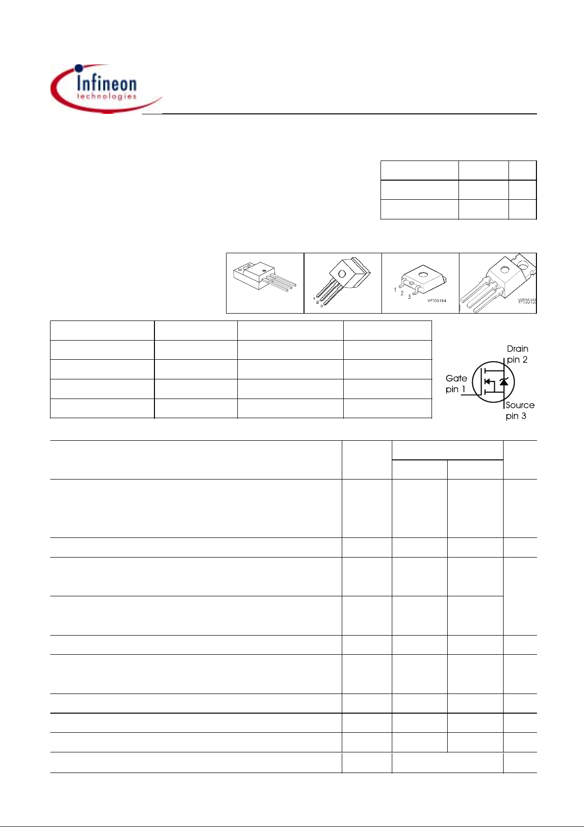
P-TO262-3-1 P-TO220-3-1P-TO220-3-31 P-TO263-3-2
• Improved transconductance
• 150 °C operating temperature
P-TO220-3-31
3
2
1
Type Package Ordering Code
SPP07N60C3 P-TO220-3-1 Q67040-S4422
SPB07N60C3 P-TO263-3-2 Q67040-S4394
SPI07N60C3 P-TO262-3-1 Q67040-S4424
SPA07N60C3 P-TO220-3-31
Q67040-S4409
Maximum Ratings
Product Summary
VDS @ T
R
I
D
Marking
07N60C3
07N60C3
07N60C3
07N60C3
DS(on
jmax
650 V
0.6 Ω
7.3 A
Parameter Symbol Value Unit
SPA
7.3
4.6
A
1)
1)
Continuous drain current
TC = 25 °C
T
= 100 °C
C
Pulsed drain current, tp limited by T
max
Avalanche energy, single pulse
ID=5.5A, VDD=50V
Avalanche energy, repetitive tAR limited by T
I
=7.3A, VDD=50V
D
Avalanche current, repetitive t
limited by T
R
Reverse diode dv/dt
IS = 7.3 A, V
< VDD, di/dt=100A/µs, T
DS
jmax
=150°C
jmax
max
2)
I
I
E
E
I
dv/dt 6 6 V/ns
Gate source voltage static V
Gate source voltage AC (f >1Hz) V
Power dissipation, T
= 25°C P
C
D
D puls
AS
AR
R
GS
GS
to
SPP_B_I
7.3
4.6
21.9 21.9 A
230 230 mJ
0.5 0.5
7.3 7.3 A
±20 ±20 V
±30 ±30
83 32 W
Operating and storage temperature T
Page 1
T
,
st
-55...+150 °C
2002-06-24

Preliminary data
A
Thermal Characteristics
Parameter Symbol Values Unit
min. typ. max.
Characteristics
Thermal resistance, junction - case R
Thremal resistance, junction - case, FullPAK R
Thermal resistance, junction - ambient, leaded R
Thermal resistance, junction - ambient, FullPAK R
SMD version, device on PCB:
R
@ min. footprint
@ 6 cm2 cooling area
3)
Linear derating factor
thJC
thJC_FP
thJ
thJA_FP
thJA
- - 1.5 K/W
- - 3.9
- - 62
- - 80
-
-
-
-
35
-
62
-
0.66
Linear derating factor, FullPAK - - 0.25
Soldering temperature,
T
sold
- - 260 °C
1.6 mm (0.063 in.) from case for 10s
Electrical Characteristics, at Tj = 25 °C, unless otherwise specified
Static Characteristics
Drain-source breakdown voltage
VGS=0V, ID=0.25mA
V
(BR)DSS
600 - - V
W/K
Drain-source avalanche breakdown voltage
VGS=0V, ID=7.3A
Gate threshold voltage, VGS = V
I
= 350 µA
D
DS
Zero gate voltage drain current
VDS = 600 V, VGS = 0 V, Tj = 25 °C
V
= 600 V, VGS = 0 V, Tj = 150 °C
DS
Gate-source leakage current
VGS=30V, VDS=0V
Drain-source on-state resistance
VGS=10V, ID=4.6A, Tj=25°C
V
=10V, ID=4.6A, Tj=150°C
GS
Gate input resistance
f = 1 MHz, open drain
Page 2
V
(BR)DS
V
GS(th)
I
DSS
I
GSS
R
DS(on)
R
G
- 700 -
2.1 3 3.9
-
-
0.5
-
1
100
- - 100 nA
-
-
0.54
1.57
0.6
1.74
- 0.8 -
2002-06-24
µA
Ω

Preliminary data
)
)
f
g
g
(
)
Electrical Characteristics
Parameter Symbol Conditions Values Unit
min. typ. max.
Characteristics
Transconductance g
Input capacitance C
Output capacitance C
Reverse transfer capacitance C
Effective output capacitance,
4)
C
energy related
Effective output capacitance,
5)
C
time related
Turn-on delay time t
Rise time t
Turn-off delay time t
Fall time t
Gate Charge Characteristics
Gate to source charge Q
Gate to drain charge Q
Gate charge total Q
fs
iss
oss
rss
o(er)
o(tr)
d(on
r
d(off
s
d
g
VDS≥2*ID*R
I
=4.6A
D
VGS=0V, VDS=25V,
f=1MHz
DS(on)max
,
- 6 - S
- 790 - pF
- 260 -
- 16 -
VGS=0V,
V
=0V to 480V
DS
- 30 -
- 55 -
VDD=380V, VGS=0/13V,
I
=7.3A,
D
R
=12Ω, Tj=125°C
G
- 6 - ns
- 3.5 -
- 60 100
- 7 15
VDD=480V, ID=7.3A - 3 - nC
- 9.2 -
VDD=480V, ID=7.3A,
V
=0 to 10V
GS
- 21 27
Gate plateau voltage V
1
Limited only by maximum temperature
2
Repetitve avalanche causes additional power losses that can be calculated as P
3
Device on 40mm*40mm*1.5mm epoxy PCB FR4 with 6cm² (one layer, 70 µm thick) copper area for drain
connection. PCB is vertical without blown air.
4
C
is a fixed capacitance that gives the same stored energy as C
o(er)
5
C
is a fixed capacitance that gives the same charging time as C
o(tr)
plateau
VDD=480V, ID=7.3A - 5.5 - V
*f.
2002-06-24
Page 3
AV=EAR
while VDS is rising from 0 to 80% V
oss
while VDS is rising from 0 to 80% V
oss
DSS
DSS
.
.
Preliminary data
Electrical Characteristics
Parameter Symbol Conditions Values Unit
min. typ. max.
Characteristics
Inverse diode continuous
I
S
TC=25°C - - 7.3 A
forward current
Inverse diode direct current,
I
SM
- - 21.9
pulsed
Inverse diode forward voltage V
Reverse recovery time t
Reverse recovery charge Q
Peak reverse recovery current I
Peak rate of fall of reverse
dirr/dt
SD
rr
rr
rrm
VGS=0V, IF=IS - 1 1.2 V
VR=480V, IF=IS ,
di
/dt=100A/µs
F
- 400 600 ns
- 4 - µC
- 28 - A
Tj=25°C - 800 - A/µs
recovery current
Typical Transient Thermal Characteristics
Symbol Value Unit Symbol Value Unit
SPP_B_I SPP_B_I
SPA SPA
R
R
R
R
R
R
th1
th2
th3
th4
th5
th6
0.024 0.024 K/W C
0.052 0.047 C
0.085 0.065 C
0.183 0.177 C
0.199 0.457 C
0.073 2.516 C
T
R
j T
th1
P
(t)
tot
C
th1
C
th2
R
C
th,n
th,n
th1
th2
th3
th4
th5
th6
0.0001354 0.00012 Ws/K
0.0004561 0.000455
0.0007717 0.000638
0.0017 0.00114
0.00778 0.00737
0.07 0.412
External Heatsink
T
case
amb
Page 4
2002-06-24
Preliminary data
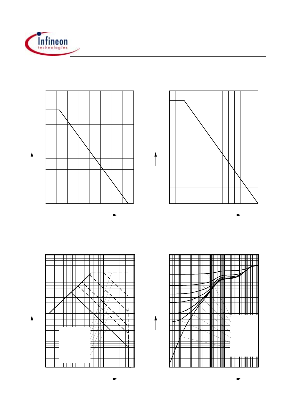
1 Power dissipation
P
= f (TC)
tot
SPP07N60C3
100
W
80
70
tot
P
60
50
40
30
20
10
0
0 20 40 60 80 100 120
°C
2 Power dissiaption FullPAK
P
= f (TC)
tot
35
W
25
tot
P
20
15
10
5
160
T
C
0
0 20 40 60 80 100 120
°C
T
150
C
3 Safe operating area FullPAK
ID = f (VDS)
parameter: D = 0, TC = 25°C
2
10
A
1
10
D
I
0
10
tp = 0.001 ms
0
tp = 0.01 ms
tp = 0.1 ms
tp = 1 ms
tp = 10 ms
DC
1
10
10
10
10
-1
-2
10
4 Transient thermal impedance FullPAK
Z
= f (tp)
thJC
parameter: D = tp/t
1
10
K/W
0
10
thJC
Z
-1
10
D = 0.5
D = 0.2
D = 0.1
-3
D = 0.05
D = 0.02
D = 0.01
single pulse
-2
10
10
-1
t
1
10
s
p
-2
10
-3
2
V
V
DS
10
3
10
10
-7
-6
-5
10
10
10
-4
10
Page 5
2002-06-24
 Loading...