

Panasonic SLSX-510 Service manual
ORDER No. AD9903088A3
Portable CD Player
SL-SX510
Colours
(S).............Silver Type
(A).............Blue Type (GK area only)
Areas
GC............Asia and Saudi Arabia
GK............China
GN............Oceania
Specification
■ Audio
No. of channels: 2 (left and right, stereo)
Frequency response: 20 to 20,000 Hz (+0.5dB, -1.5dB)
Output voltage: 0.6 V (50kΩ)
S/N: More than 96 dB*
Wow and flutter: Below measurable limit
DA converter: 1bit,MASH
Headphones output level: Max. 9mW+9mW/16Ω (variable)
■ Pickup
Light source: Semiconductor laser
Wavelength: 780 nm
■ General
Operational temperature range: 0°C - 40°C
Rechargeable temperature range: 5°C - 40°C
Power supply: DC 4.5 V
● Power consumption:
Power source Anti-shock off/on
When using AC adaptor 2.8W/3.0W
When recharging: Approx. 5.4W
● Play time:
(When used in hold mode, at 25°C temperature and on a flat and
stable surface)
Batteries used Anti-shock off/on
2 Alkaline batteries (LR03) About 9h/About 12h
2 Alkaline batteries (LR6) Ab out 22h/About 28h
Rechargeable batteries About 6h/About 8h
4 Alkaline batteries About 33h/About 43h
2 Rechargeable and 2 Alkaline
batteries
The play time may be less depending on the operating conditions.
Recharging time: About 3h
Dimensions (WxHxD): 128x20.8x131 mm
Weight: 191g (with batteries)
*These specifications were measured in the Anti-shock off mode.
Note:
Specifications are subject to change without notice.
Weight and dimensions are approximate.
About 28h/About 36h
169g (without batteries)
© 1999 Matsushita Electric Industrial Co., Ltd. All
rights reserved. Unauthorized copying and
distribution is a violation of law.

SL-SX510
CONTENTS
Page Page
1 Simplement Guide 2
2 Accessories
3 Schematic Diagram Notes
3.1. Schematic Diagram Notes
3.2. Type Illustration of ICエs, Transistors and Diodes
4 Schematic Diagram
5 Printed Circuit Board and Wiring Connection Diagram 10
2
6 Replacement Parts List
3
3
3
4
6.1. Electrical Parts List (Original)
6.2. Cabinet and Chassis Parts List (Original)
6.3. Packaging and Accessories Parts List (Original)
1 Simplement Guide
This manual mention the revision of SL-SX510.
· Accessories
· Schematic Diagram (Original)
· Printed Circuit Board Diagram (Original)
· Replacement Parts List
Electrical Parts List (Original)
Cabinet and Chassis Parts List (Original)
Packaging and Accessories Parts List (Original)
The other items are refered service manual for SL-SX510.
12
12
14
15
2 Accessories
· AC adaptor ...................................... 1 pc.
· Stereo earphones ............................ 1 pc.
For areas (GC) and (GK)
− Cord clip .................................... 1 pc.
· Wired remote control ....................... 1 pc.
· External battery case ....................... 1 pc.
· Nickel-metal hydride batteries .......... 2 pcs.
· Battery carrying case ....................... 1 pc.
Remove the rechargeable batteries from their case
before use. If the inner tray is removed, the case
can be use to carry 2 LR6 (UM-3) batteries, used
in the external battery case.
· Soft case ......................................... 1 pc.
For area (GC)
· Power plug adaptor ......................... 1 pc.
2
3 Schematic Diagram Notes
C
C
Ca
a
1
5
24
13
20
17
12
8
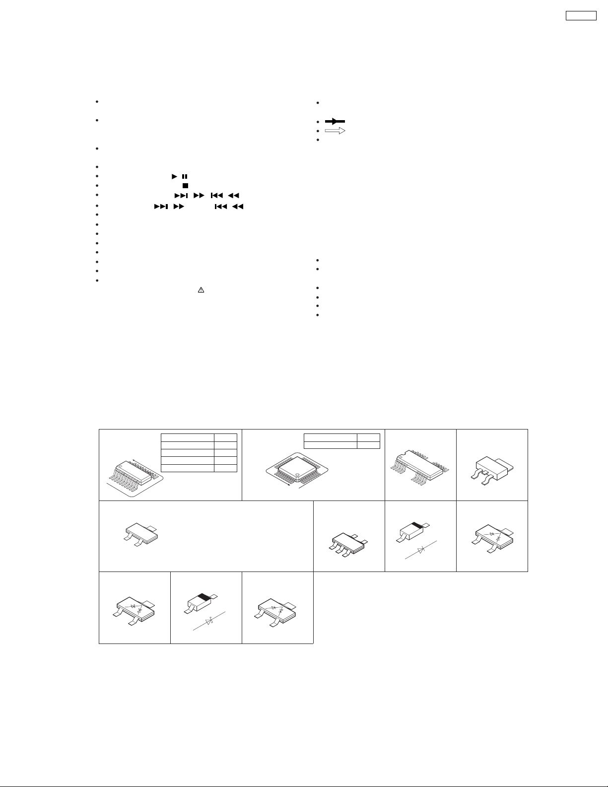
3.1. Schematic Diagram Notes
Notes:
S201 : Laser ON/OFF switch in “OFF” position.
(It turns “ON” with disc holder closed.)
S202: Rest detector in “OFF” position.
(It turns “ON” when optical pickup comes to
innermost periphery.)
S309 : Play mode selector (MODE) in “NORMAL” position.
(RANDOM
S310 : Hold (HOLD) switch in “OFF” position.
S801 : Play/pause (
S802 : Stop/power off (
S803,: Skip/search (
S804 [S803 :
S805 : Repeat (REPEAT) switch.
S806 : Memory/recall (MEMORY/RECALL) switch.
S807 : EQ selector (EQ)switch.
S808 : Anti-shock (A.SHOCK) switch.
S809 : Battery check (BATT CHECK) switch.
VR11 : Power supply voltage adjustment.
VR701-1, 2 : Headphones volume (VOLUME) control.
Important safety notice:
Components identified by
istics important for safety.
Furthermore, special parts which have purposes of fire-re-
tardant (resistors), high-quality sound (capacitors), lownoise (resistors), etc. are used. When replacing any of components, be sure to use only manufacture’s specified parts
shown in the parts list.
⇔
NORMAL ⇔ RESUME)
/ ) switch.
/ POWER OFF) switch.
/ , / ) switches.
/ , S804 : / ]
mark have special character-
The supply part number is described alone in the replace ment parts.
: +B lines.
: CD playback signal lines.
The voltage value and waveforms are the reference voltage
of this measured by DC electronic voltmeter (high impedance)
and oscilloscope on the basis of GND terminal (DC IN Jack).
Accordingly, there may arise some errors in the voltage val-
ues and waveforms depending upon the internal impedance
of the tester or measuring unit.
Measurement conditions:
AC adaptor is used for power supply.
*
Set the headphones VR(VR701) to center position(No.5).
*
Set the hold lock and ANTI-SHOCK switches to ON.
*
The parenthesized is the voltage for test disc (1 kHz, L+R,
*
0 dB) in play mode, and the other , f or no disc in stop mode.
Caution!!
IC and LSI are sensitive to static electricity.
Secondary trouble can be prevented by taking care during
repair.
Cover the parts boxes made of plastics with aluminum foil.
Ground the soldering iron.
Put a conductive mat on the work table.
Do not touch the pins of IC or LSI with fingers directly.
SL-SX510
3.2. Type Illustration of IC´s, Transistors and Diodes
C
C
MNA4400T10T
A
Anode
A
A
No.1
B
MA741WKTX
A
Anode
Anode
NJU7082BVTE1
AN8839NSBE1
RS10002E2
BH6522FVE2
BA6966FVE2
C
E
MSB709RST1
2SB1218ATX
2SD1328TX
2SD1819ATX
MA1070400L
Cathode
Ca
A
Anode
A
A
A
8PIN
28PIN
40PIN
40PIN
20PIN
Cathode
Ca
Ca
Ca
DTA114YUA106
DTC114EUA106
DTC144TUA106
UN5213TX
MA143TX
A
Anode
Ca
Cathode
No.1
Cathode
Ca
Anode
A
SC440323CFU
MN662782RPT1
XN1210TX
XN1215TX
B
E
E
B
B
64PIN
80PIN
Cathode
C
Ca
2SB1182TLPQR
B
E
MA142WKTXMA111TX
A
Anode
A
Anode
C
Cathode
Ca
3
SL-SX510
4 Schematic Diagram
OPERATION/ LCDUNIT
LCD301 (RSL5217
1 2 3 4 5 6 7 8 9 10 11 12 13 14 1516 17 18 19 20
TS A
S808
(A.SHOCK)
S805
(REPEAT)
S803
(/)
S801
()
S809
(BATTERY
CHECK)
S802
( POWER OFF)
S804
(/)
S806
(MEMORY/
RECALL)
S807
(EQ)
T)
LCD DISPLAY
RQPONML K J IHGFEDCB
A
B
C
D
E
F
A
B
C
:POSITIVE VOLTAGELINE
30
29
28
27
26
25
24
23
22
21
20
19
18
17
16
15
14
13
12
11
10
9
8
7
6
5
4
3
2
1
CN301
I
H
G
F
E
D
T
S
R
Q
P
O
N
M
L
K
J
I
H
G
F
E
D
C
B
A
C
B
A
Q201
MSB709RST1
LASER POWER
DRIVE
(2.4V)
2.5V
0.8V
R201
2.2
30
A
B
C
D
E
F
A
B
C
D
E
F
G
H
I
J
K
L
M
N
O
P
Q
R
S
T
A
B
C
29
28
27
26
25
24
23
22
21
20
19
18
17
16
15
14
13
12
11
10
9
8
7
6
5
4
3
2
1
:CD PLAYBACK SIGNAL LINE
2.5V
SHORT LAND
TRAVERSEUNIT
( OPTICALPICKUP)
0.22
6 7 8 9 10
CC
V
GND F
E
0.047
B
LD
VREFALPD
0.22
TRACKING
COIL
FOCUS
COIL
22K
R202
2V
(1.4V)
D
C
B
A
GND
GND
1
12345
2K
A
B
C
D
2
RF(
3
V
4
TE(F)
5
GND
6
TE(E)
7
VREF
8
9
LPD
10
11
GND
12
13
14
15
16
CN101
1
LD
2
A)
3
CC
4
5
6
7
8
A
9
10
NC
11
12
T
13
T
14
F
15
F
16
33
33
R113
R114
A
B
C
D
E
A
B
C
D
C201
R203
6.3V22
1
(LASER ON/OFF)
2.5V
S201
4

SL-SX510
:CD PLAYBACK SIGNAL LINE:POSITIVE VOLTAGELINE
3.2V
2.5V
R306
47K
C301
JI GFEDCB
KH A
1.6V
1.6V
1.6V
1.6V
1.6V
1.6V
1.6V
1.6V
1.6V
1.6V
1.6V0V0V
3.1V (0V)
FP7
FP8
FP9
FP11
FP10
FP12
FP13
FP14
FP15
FP16
FP17
3V
2V
1V
0V
MCLK
3.1V
T
PLAY
13.3ms.
MEMORY
REPEAT
SKIP.R
3.1V
3.1V
FP18
TXPOWER/REMSEL
SKIP.F
3.1V
3.1V
1.6V
1
1.6V
1.6V
1.6V
1.6V
1.6V
1.6V
1.6V
1.6V
2.1V
3.2V
1.5V
1.9V
1V
R301
3.9K
FP6
2
FP5
3
FP4
4
5
6
7
8
9
10
11
12
13
14
15
16
C302
FP3
FP2
FP1
BP3/FP0
BP2
BP1
BP0
VCLD3
VCLD2
VCLD1
V
OSC1
OSC2
1
T 15.2ms.
IC301
SC440323CFU
SYSTEM CONTROL / LCD DRIVE
PLAY
F=75Hz
XOSC2
XOSC1
2.9V
2.4V
0V
VSSRESET
BLKCK
0V
2.9V
STAT
MDATA
2.5V
(1.5V) 0V
DD
17 18 19 20 21 2223 24 25 26 2728 29 30 31 32
AG FBEFBCDE IADGCH
2.5V
L
M
N
O
P
Q
R
S
T
1M
R304
R302
100K
0.1
3.2V [GC,GK]
0V [GN]
R307 100K
49505152535455565758596061626364
MUTE
PDOWN
MEMORY
/LCDREM
ZANSEL
/RANSEL
RSENSE
STROBE2/RDATA
STROBE1/RCLK
HOLD
RESUME
RANDOM
BATTSTROBE
3V
PLAY
REST
0V
OPEN
BOUT
SHOCK.P
STOP
BATTERY
EQ
3.1V
3.1V
3.1V
MLD
BUZ
PC
FG
D302
0V
48
0V
47
0.2V
46
0V
45
3.1V
44
3.1V
43
3.1V
42
3.1V
41
0V (3.1V)
40
3.1V
39
0V
38
3.2V
37
3.1V
36
0V (3.1V)
35
2.5V
34
3.1V
33
MA142WKTX
R905
AB
47K
C DEFGH
B
A
D301
MA142WKTX
R303
1K
S310
(HOLD)
ON OFF
S309
(MODE)
NORMAL RANDOMRESUME
C
B
D
A
E
C114
PLAY
0.5 s. 0.2V/DIV.
0.8V
P
0.1
C115 0.022
C103 0.022
P
RF
C503
R125 120K
R126 120K
C101
0.1
560P
ABC
IC101
AN8839NSBE1
SERVOAMP
1
PDE FBAL
1.2V
2
PDF
2.5V
3
V
DD
1.2V
4
PDA
1.2V
5
PDB
0V
6
LPD
(1.4V)
2V
7
LD
(1.2V)
0.6V
8
RF
0.7V
9
RF IN
1.2V
10
CSBRT
0.9V
11
CEA
0V
12
BDO
(2.7V)
0V
13
LDON
14 15
GND
TBAL
VREF
FE IN
FE OUT
TE OUT
TE IN
ENVOFF
ENV
OFTR
PDOWN
/RFDET
2.5V
PLAY
50mV
P
C112
C121
220P
120P
P
For [GC,GK] areas.
3.2V
10K
47K
0V
(3.1V)
3.1V
S
0.1
C552
Q551
DTA114YUA106
POWER SUPPLY
JK551
OPTOUT
R122
120K
R120
10K
R121
120K
R127
47K
C111
0.022
RJ2
0
C120
1500P
0.1
C113
PLAY
2ms. 0.1V/DIV.
D
E
F
G
For [GN]
H
area.
I
J
K
0.4V
P
P
R309
100K
(0V)
3.2V
R551
C551
1K
0.1
2ms. 20mV/DIV.
1.2V1.2V
28
1.2V
27
1.2V
26
1.2V
25
1.2V
24
1.2V
23
1.2V
22
21
NC
(0V)
3.1V
20
1.2V
19
18
NC
0V
17
0V
16
(0V)
2.4V
5
 Loading...