

Panasonic SA-XH50P, SA-XH50PC, SB-HS70, SB-HF70, SB-HC70 Service Manual
...
© Panasonic Corporation 2011. All rights reserved.
Unauthorized copying and distribution is a violation
of law.
PSG1104002CE
A6
DVD Home Theater Sound System
Model No. SA-XH50P
SA-XH50PC
Product Color: (K)...Black Type
TABLE OF CONTENTS
PAGE PAGE
1 Safety Precautions----------------------------------------------- 3
1.1. GENERAL GUIDELINES--------------------------------3
1.2. Before Repair and Adjustment------------------------- 4
1.3. Protection Circuitry----------------------------------------5
1.4. Safety Parts Information--------------------------------- 5
2 Warning-------------------------------------------------------------- 6
2.1. Prevention of Electrostatic Discharge (ESD)
to Electrostatic Sensitive (ES) Devices---------------6
2.2. Precaution of Laser Diode-------------------------------7
2.3. Service caution based on Legal restrictions --------8
2.4. Handling Precautions for Traverse Unit--------------9
3 Service Navigation --------------------------------------------- 11
Note: Please refer to the original service manual for:
O DVD Mechanism Unit (BRS1D), Order No. PSG1012001CE
O Speaker system SB-XH50P/PC-K, Order No. PSG1103007CE

2
3.1. Service Information-------------------------------------- 11
4 Specifications----------------------------------------------------12
4.1. Others (Licences) ----------------------------------------13
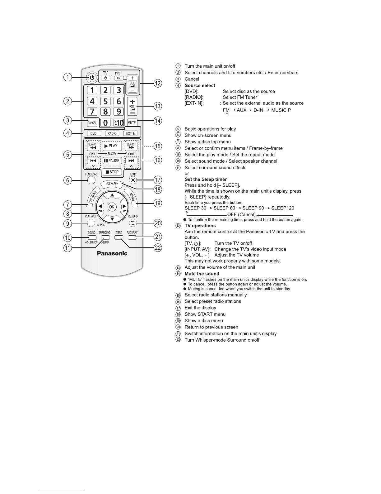
5 Location of Controls and Components------------------14
5.1. Remote Control and Main Unit Key Button
Operations -------------------------------------------------14
5.2. Main Unit Key Button Operations --------------------15
5.3. Power-Saving Features --------------------------------15
5.4. Speaker Connection-------------------------------------16
5.5. Linked Operations with the TV (VIERA LINK
“HDAVI Control™”) --------------------------------------17
5.6. Connection with an ARC compatible TV -----------19
5.7. Disc Information ------------------------------------------20
6 Operating Instructions----------------------------------------22
6.1. Removing of disc during abnomality ----------------22
7 Self-Diagnostic and Special Mode Setting ------------- 24
7.1. Cold-Start---------------------------------------------------24
7.2. Service Mode Table--------------------------------------24
7.3. Self-Diagnostic Mode -----------------------------------30
7.4. Self Diagnostic Function-Error Code----------------31
7.5. Sales Demonstration Lock Function ----------------33
7.6. Firmware Version-Up Information--------------------34
8 Troubleshooting Guide----------------------------------------36
8.1. Troubleshooting Guide for F61 and/or F76--------36
8.2. DVD/CD Laser Diode current
measurement.This section will illustrate
proceddures of measuring& deriving DVD/CD
Laser Diode Current.------------------------------------39
8.3. Basic Troubleshooting Guide for Traverse
Unit (Backend P.C.B.)-----------------------------------41
8.4. Basic Troubleshooting Guide for HDMI AV
output--------------------------------------------------------42
9 Service Fixture & Tools---------------------------------------43
9.1. Service Tools and Equipment-------------------------43
10 Disassembly and Assembly Instructions---------------44
10.1. Disassembly Flow Chart--------------------------------45
10.2. Main Components and P.C.B. Locations-----------46
10.3. Disassembly of Top Cabinet---------------------------47
10.4. Disassembly of Rear Panel----------------------------48
10.5. Disassembly of Front Panel Assembly -------------48
10.6. Disassembly of Panel P.C.B.--------------------------49
10.7. Disassembly of Power Button P.C.B.----------------51
10.8. Disassembly of DVD Mechanism Unit
(BRS1D)----------------------------------------------------52
10.9. Replacement of Traverse unit-------------------------54
10.10. Disassembly of Main P.C.B.---------------------------59
10.11. Replacement of Digital Amplifier IC (IC403/
IC404/IC405)----------------------------------------------61
10.12. Disassembly of SMPS P.C.B.-------------------------63
10.13. Replacement of Current Limiting Switch
(Q5701)-----------------------------------------------------65
10.14. Replacement of Diode (D5706) ----------------------66
10.15. Disassembly of Backend P.C.B.----------------------67
11 Service Position -------------------------------------------------69
11.1. Checking & Repairing Main P.C.B. (Side B)-------69
11.2. Checking & Repairing Main P.C.B. (Side A)-------69
11.3. Checking & Repairing of SMPS P.C.B.-------------70
11.4. Checking & Repairing of Panel P.C.B.-------------- 7 0
11.5. Checking & Repairing of DVD Module P.C.B.-----70
12 Voltage & Waveform Chart-----------------------------------72
12.1. Backend P.C.B. (1/3)------------------------------------72
12.2. Backend P.C.B. (2/3)------------------------------------ 73
12.3. Backend P.C.B. (3/3)------------------------------------ 74
12.4. Main P.C.B. (1/3)----------------------------------------- 75
12.5. Main P.C.B. (2/3)----------------------------------------- 76
12.6. Main P.C.B. (3/3)----------------------------------------- 77
12.7. Panel P.C.B.----------------------------------------------- 78
12.8. SMPS P.C.B.---------------------------------------------- 78
12.9. Waveform Table (1/2)----------------------------------- 79
12.10. Waveform Table (2/2)----------------------------------- 80
13 Illustration of ICs, T ransistor and Diode---------------- 81
14 Overall Simplified Block Diagram------------------------- 83
15 Block Diagram--------------------------------------------------- 84
15.1. Backend---------------------------------------------------- 84
15.2. IC Terminal Chart---------------------------------------- 85
15.3. System Control------------------------------------------- 86
15.4. Audio & Video -------------------------------------------- 87
15.5. Power Supply--------------------------------------------- 89
16 Wiring Connection Diagram -------------------------------- 91
17 Schematic Diagram-------------------------------------------- 93
17.1. Schematic Diagram Notes ---------------------------- 93
17.2. Backend Circuit ------------------------------------------ 95
17.3. Main Circuit-----------------------------------------------101
17.4. Panel & Power Button Circuit------------------------109
17.5. SMPS Circuit---------------------------------------------110
18 Printed Circuit Board-----------------------------------------112
18.1. Backend P.C.B.------------------------------------------112
18.2. Main P.C.B.-----------------------------------------------113
18.3. Panel & Power Button P.C.B.------------------------ 115
18.4. SMPS P.C.B.---------------------------------------------116
19 Terminal Function of ICs -----------------------------------117
19.1. IC200 (RFKWMXH50EB): IC
MICROPROCESSOR ---------------------------------117
19.2. IC6001 (C0HBB0000057): IC FL Display
Driver ------------------------------------------------------118
20 Exploded View and Replacement Parts List----------119
20.1. Exploded View and Mechanical Replacement
Parts List--------------------------------------------------119
20.2. Electrical Replacement Parts List ------------------123
3
1 Safety Precautions
1.1. GENERAL GUIDELINES
1. When servicing, observe the original lead dress. If a short circuit is found, replace all parts which have been overheated or
damaged by the short circuit.
2. After servicing, see to it that all the protective devices such as insulation barriers, insulation papers shields are properl y
installed.
3. After servicing, carry out the following leakage current checks to prevent the customer from being exposed to shock hazards.
1.1.1. LEAKAGE CURRENT COLD CHECK
1. Unplug the AC cord and connect a jumper between the two prongs on the plug.
2. Measure the resistance value, with an ohmmeter, between the jumpered AC plug and each exposed metallic cabinet part on
the equipment such as screwheads, connectors, control shafts, etc. When the exposed metallic part has a return path to the
chassis, the reading should be between 1MΩ and 5.2MΩ.
When the exposed metal does not have a return path to the chassis, the reading must be
(This “Safety Precaution” is applied only in U.S.A.)
1. Before servicing, unplug the power cord to prevent an electric shock.
2. When replacing parts, use only manufacturer’s recommended components for safety.
3. Check the condition of the power cord. Replace if wear or damage is evident.
4. After servicing, be sure to restore the lead dress, insulation barriers, insulation papers, shields, etc.
5. Before returning the serviced equipment to the customer, be sure to make the following insulation resistance test to prevent
the customer from being exposed to a shock hazard.
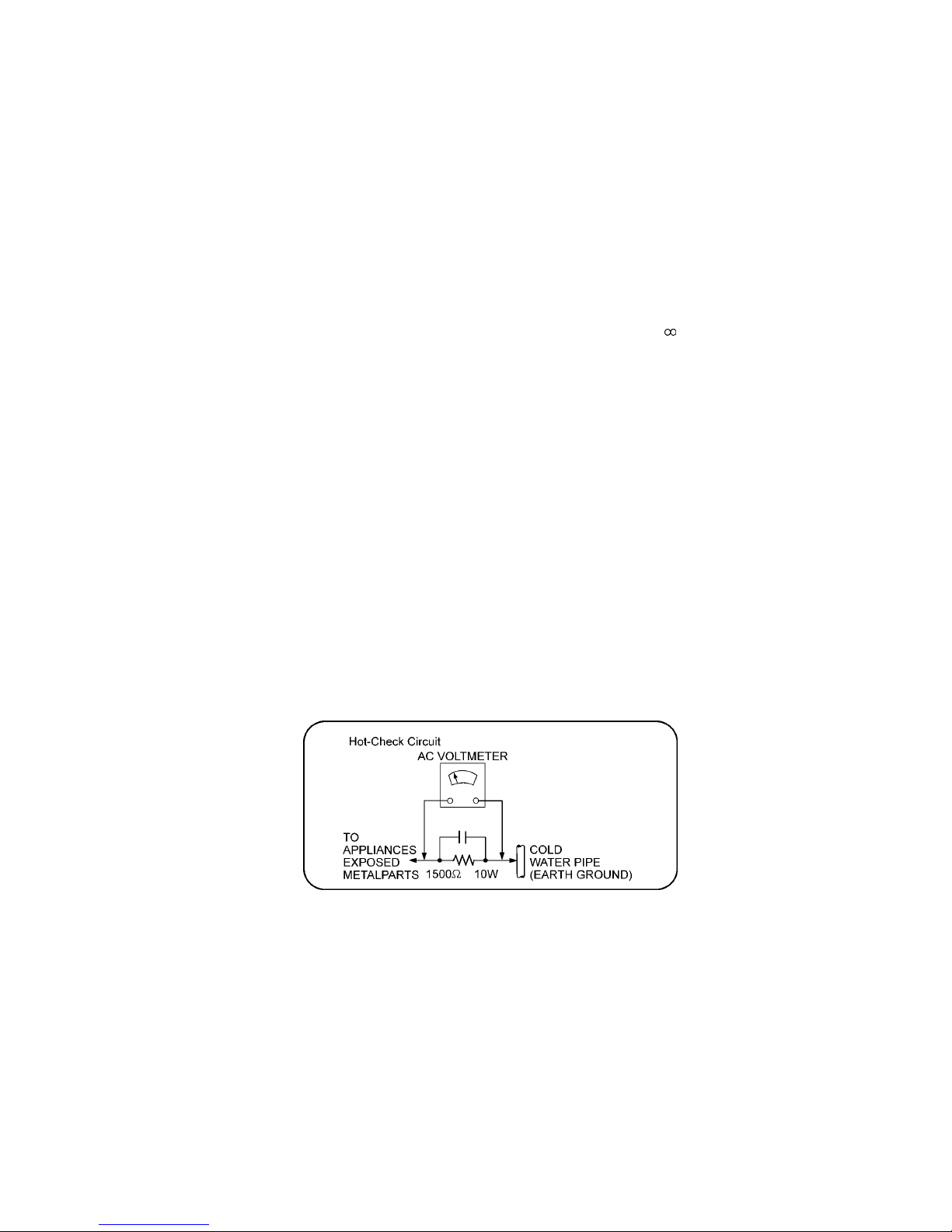
1.1.2. LEAKAGE CURRENT HOT CHECK
1. Plug the AC cord directly into the AC outlet. Do not use an isolation transformer for this check.
2. Connect a 1.5kΩ, 10 watts resistor, in parallel with a 0.15µF capacitors, between each exposed metallic part on the set and a
good earth ground such as a water pipe, as shown in Figure 1.
3. Use an AC voltmeter, with 1000 ohms/volt or more sensitivity, to measure the potential across the resistor.
4. Check each exposed metallic part, and measure the voltage at each point.
5. Reverse the AC plug in the AC outlet and repeat each of the above measurements.
6. The potential at any point should not exceed 0.75 volts RMS. A leakage current tester (Simpson Model 229 or equivalent)
may be used to make the hot checks, leakage current must not exceed 1/2 milliamp. In case a measurement is outside of the
limits specified, there is a possibility of a shock hazard, and the equipment should be re paired and rechecked before it is
returned to the customer.
Figure 1
4
1.2. Before Repair and Adjustment
Disconnect AC power to discharge unit AC Capacitors as such (C5702, C5703, C5704, C5705, C5706) through a 10 Ω, 10 W resistor to ground.
Caution:
DO NOT SHORT-CIRCUIT DIRECTLY (with a screwdriver blade, for instance), as this may destroy solid state devices.
After repairs are completed, restore power gradually using a variac, to avoid overcurrent.
Current consumption at AC 120V, 60 Hz in NO SIGNAL mode at volume minimal should be ~ 200 mA.
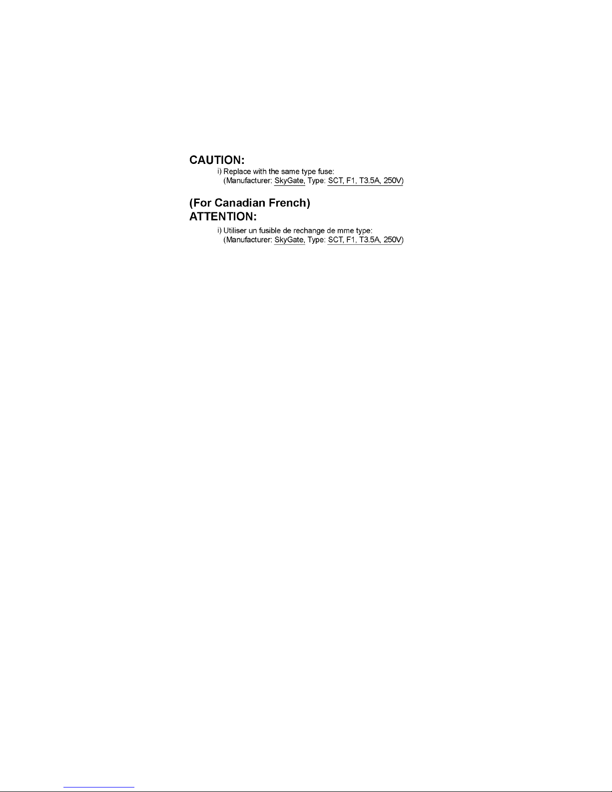
1.2.1. Caution for fuse replacement

5
1.3. Protection Circuitry
The protection circuitry may have operated if either of the following conditions are noticed:
• No sound is heard when the power is turned on.
• Sound stops during a performance.
The function of this circuitry is to prevent circuitry damage if, for example, the positive and negative speaker connection wires are
“shorted”, or if speaker systems with an impedance less than the indicated rated impedance of the amplifier are used.
If this occurs, follow the procedure outlines below:
1. Turn off the power.
2. Determine the cause of the problem and correct it.
3. Turn on the power once again after one minute.
Note:
When the protection circuitry functions, the unit will not operate unless the power is first turned off and then on again.
1.4. Safety Parts Information
Safety Parts List:
There are special components used in this equipment which are important for safety.
These parts are marked by in the Schematic Diagrams, Exploded View & Replacement Parts List. It is essential that these
critical parts should be replaced with manufacturer’s specified parts to prevent shock, fire or other hazards. Do not modify the
original design without permission of manufacturer.
Safety Ref No. Part No. Part Name & Description Remarks
8 RGRX1004B-A REAR PANEL P
8 RGRX1004B-B1 REAR PANEL PC
20 RKMX1009-K TOP CABINET
25 RMNX1075 TOP CABINET INSULATOR SHEET
29 RSCX1059 BACKEND PCB SHIELD PLATE
35 RMNX1050 BOTTOM PC SHEET
301 RAY1101-V TRAVERSE ASS'Y
A2 K2CB2CB00021 AC CORD
A3 RQTX1326-P O/I BOOK (En)
A3 RQTX1327-C O/I BOOK (Cf) PC
PCB4 REPX0933B SMPS P.C.B. (RTL)
DZ5701 ERZVA5Z471 ZNR
L5701 ELF17N010A LINE FILTER
L5702 ELF19H010A LINE FILTER
T2900 G4D1A0000118 SWITCHING TRANSFORMER
T5701 ETS35BL136AC MAIN TRANSFORMER
PC701 B3PBA0000503 PHOTO COUPLER
F1 K5G312Y00007 FUSE PROTECTOR
TH5701 D4CC11040013 THERMISTOR
TH5702 D4CAA5R10001 THERMISTOR
P5701 K2AB2B000007 AC INLET
C5702 F0CAF104A105 0.1uF
C5703 F0CAF104A105 0.1uF
C5704 F1BAF471A013 470pF
C5705 F1BAF471A013 470pF
C5706 F1BAF1020020 1000pF

6
2Warning
2.1. Prevention of Electrostatic Discharge (ESD) to Electrostatic Sensitive
(ES) Devices
Some semiconductor (solid state) devices can be damaged easily by static electricity. Such components commonly are called Electrostatically Sensitive (ES) Devices. Examples of typical ES devices are integrated circuits and some field-effect transistors and
semiconductor “chip” components. The following techniques should be used to help reduce the incidence of component damage
caused by electrostatic discharge (ESD).
1. Immediately before handling any semiconductor component or semiconductor-equipped assembly, drain off any ESD on your
body by touching a known earth ground. Alternatively, obtain and wear a commercially available discharging ESD wrist strap,
which should be removed for potential shock reasons prior to applying power to the unit under test.
2. After removing an electrical assembly equipped with ES devices, place the assembly on a conductive surface such as aluminum foil, to prevent electrostatic charge build up or exposure of the assembly.
3. Use only a grounded-tip soldering iron to solder or unsolder ES devices.
4. Use only an anti-static solder removal device. Some solder removal devices not classified as “anti-static (ESD protected)” can
generate electrical charge sufficient to damage ES devices.
5. Do not use freon-propelled chemicals. These can generate electrical charges sufficient to damage ES devices.
6. Do not remove a replacement ES device from its protective package until immediately before you are ready to install it. (Most
replacement ES devices are packaged with leads electrically shorted together by conductive foam, aluminum foil or comparable conductive material).
7. Immediately before removing the protective material from the leads of a replacement ES device, touch the protective material
to the chassis or circuit assembly into which the device will be installed.
Caution:
Be sure no power is applied to the chassis or circuit, and observe all other safety precautions.
8. Minimize bodily motions when handling unpackaged replacement ES devices. (Otherwise harmless motion such as the
brushing together of your clothes fabric or the lif ting of your foot from a carpeted floor can generate static electricity (ESD) sufficient to damage an ES device).
7
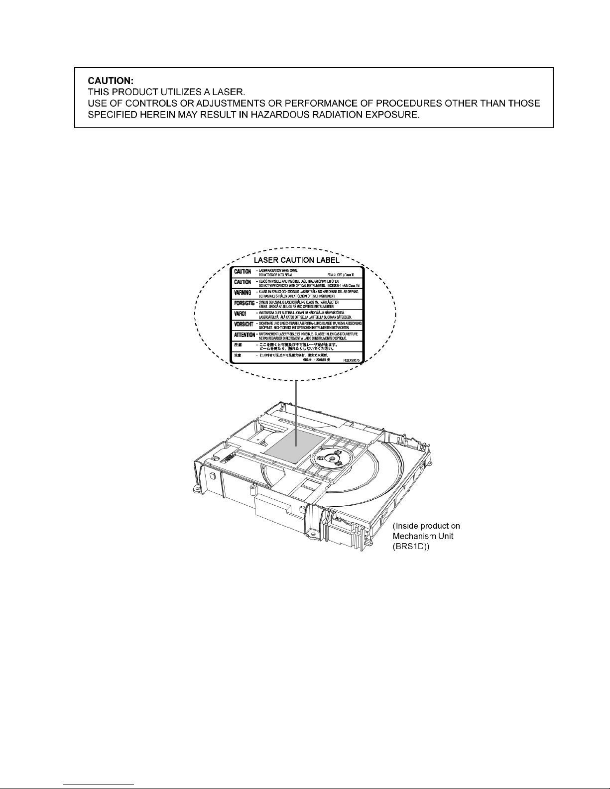
2.2. Precaution of Laser Diode
Caution:
This product utilizes a laser diode with the unit turned “on”, invisible laser radiation is emitted from the pickup lens.
Wavelength: 655 nm (DVD)/790 nm (CD)
Maximum output radiation power from pickup: 100 µW/VDE
Laser radiation from the pickup unit is safety level, but be sure the followings:
1. Do not disassemble the pickup unit, since radiation from exposed laser diode is dangerous.
2. Do not adjust the variable resistor on the pickup unit. It was already adjusted.
3. Do not look at the focus lens using optical instruments.
4. Recommend not to look at pickup lens for a long time.
8
2.3. Service caution based on Legal restrictions
2.3.1. General description about Lead Free Solder (PbF)
The lead free solder has been used in the mounting process of all electrical components on the printed circuit boards used for this
equipment in considering the globally environmental conservation.
The normal solder is the alloy of tin (Sn) and lead (Pb). On the other hand, the lead free solder is the alloy mainl y consists of tin
(Sn), silver (Ag) and Copper (Cu), and the melting point of the lead free solder is higher approx.30 degrees C (86°F) more than that
of the normal solder.
Definition of PCB Lead Free Solder being used
Service caution for repair work using Lead Free Solder (PbF)
• The lead free solder has to be used when repairing the equipment for which the lead free solder is used.
(Definition: The letter of “PbF” is printed on the PCB using the lead free solder.)
• To put lead free solder, it should be well molten and mixed with the original lead free solder.
• Remove the remaining lead free solder on the PCB cleanly for soldering of the new IC.
• Since the melting point of the lead free solder is high er than that of the normal lead solder, it takes the longer time to melt the
lead free solder.
• Use the soldering iron (more than 70W) equipped with th e temperature contro l after setting the temperature at 350±30 degrees
C (662±86°F).
Recommended Lead Free Solder (Service Parts Route.)
• The following 3 types of lead free solder are available through the service parts route.
RFKZ03D01K-----------(0.3mm 100g Reel)
RFKZ06D01K-----------(0.6mm 100g Reel)
RFKZ10D01K-----------(1.0mm 100g Reel)
Note
* Ingredient: tin (Sn), 96.5%, silver (Ag) 3.0%, Copper (Cu) 0.5%, Cobalt (Co) / Germanium (Ge) 0.1 to 0.3%
The letter of “PbF” is printed either foil side or components side on the PCB using the lead free solder.
(See right figure)
9
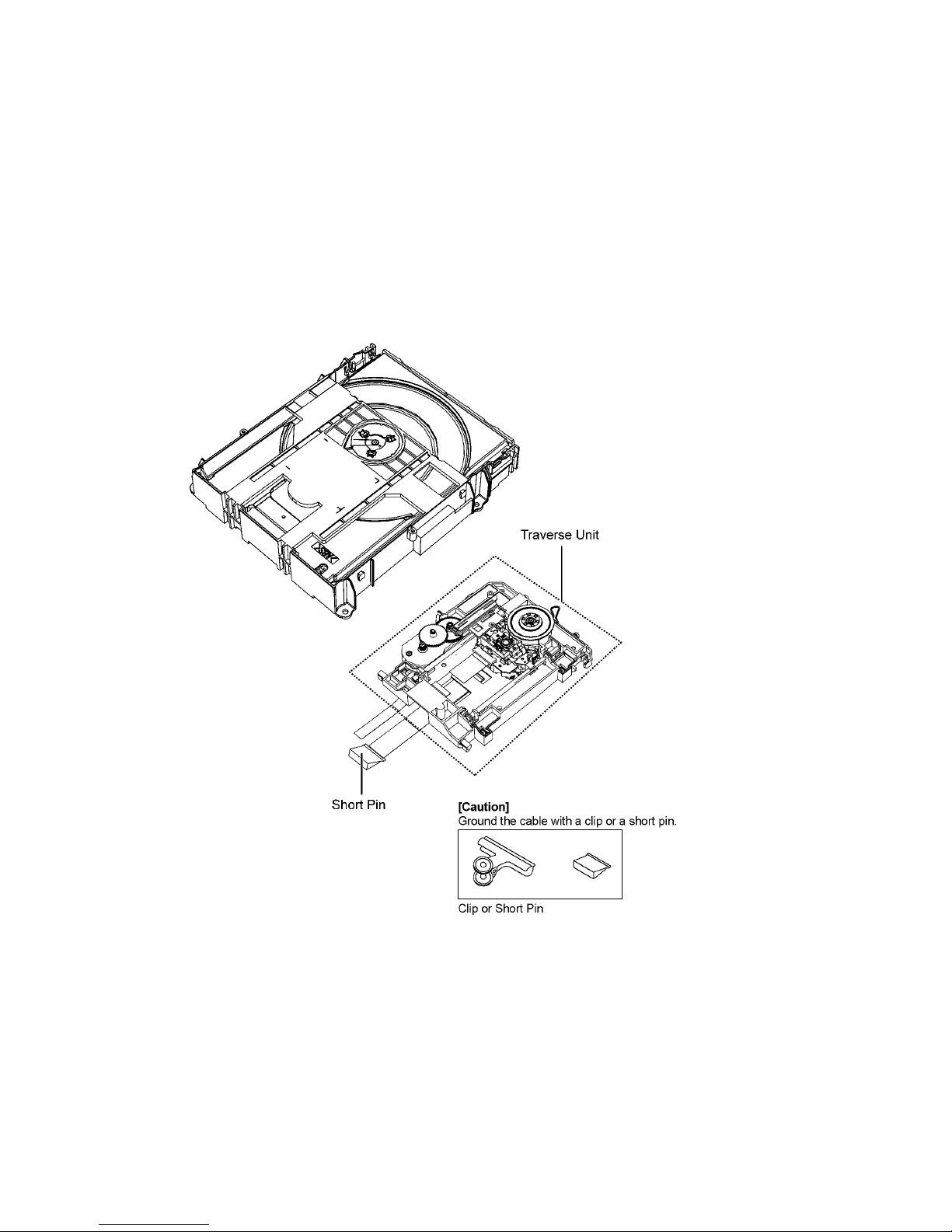
2.4. Handling Precautions for Traverse Unit
The laser diode in the optical pickup unit may break down du e to static electricity of clothes or human body. Special care must be
taken avoid caution to electrostatic breakdown when servicing and handling the laser diode in the traverse unit.
2.4.1. Cautions to Be Taken in Handling the Optical Pickup Unit
The laser diode in the optical pickup unit ma y be damaged due to ele ctrostatic discharge generating from clothes or human body.
Special care must be taken avoid caution to electrostatic discharge damage when servicing the laser diode.
1. Do not give a considerable shock to the optical pickup unit as it has an extremely high-precise structure.
2. To prevent the laser diode from the electrostatic discharge damage, the flexible cable of the optical pickup unit removed
should be short-circuited with a short pin or a clip.
3. The flexible cable may be cut off if an excessive force is applied to it. Use caution when handling the flexible cable.
4. The antistatic FPC is connected to the new optical pickup unit. After replacing the optical pickup unit and connecting the flexible cable, cut off the antistatic FPC.
Figure 1
2.4.2. Grounding for electrostatic breakdown prevention
Some devices such as the DVD player use the optical pickup (laser diode) and the optical pickup will be damaged by static electricity in the working environment. Proceed servicing works under the working environment where grounding works is completed.
2.4.2.1. Worktable grounding
1. Put a conductive material (sheet) or iron sheet on the area where the optical pickup is placed, and ground the sheet.

10
2.4.2.2. Human body grounding
1. Use the anti-static wrist strap to discharge the static electricity form your body.
Figure 2

11
3 Service Navigation
3.1. Service Information
This service manual contains technical information which will allow service personnel’s to understand and service this model.
Please place orders using the parts list and not the drawing reference numbers.
If the circuit is changed or modified, this information will b e followe d by supplemen t service manual to b e filed with o riginal se rvice
manual.
• DVD Mechanism Unit (BRS1D):
1) This model uses DVD Mechanism Unit (BRS1D).
• Micro-processor:
1) The following components are supplied as an assembled part.
• Micro-processor IC, IC200 (RFKWMXH50EB)
12
4 Specifications
Main unit SA-XH50P/PC
OGENERAL
Power supply: AC 120 V, 60 Hz
Power consumption: Main Unit 47 W
Power Consumption in standby mode:
approx. 0.4 W
Dimensions (W×H×D): 360 mm × 48 mm × 273 mm
(14
13
/16” x 17/8” X 103/4”)
Mass [Weight] Main unit 2 kg (4.4 lbs)
Operating temperature range:
0 °C to +40 °C
(+32 °F to +104 °F)
Operating humidity range: 35 % to 80 % RH
(no condesation)
OAMPLIFIER SECTION
RMS Output Power: Dolby Digital Mode
Front Ch:
55 W per channel (5 Ω), 1 kHz, 10% THD
Surround Ch:
55 W per channel (5 Ω), 1 kHz, 10% THD
Center Ch:
55 W per channel (5 Ω), 1 kHz, 10% THD
Subwoofer Ch:
55 W per channel (5 Ω), 100 Hz, 10% THD
Total RMS Dolby Digital mode power:
330 W
FTC Output Power: Dolby Digital Mode
Front Ch:
25 W per channel (5 Ω), 120 Hz to 20 kHz, 1 % THD
Surround Ch:
25 W per channel (5 Ω), 120 Hz to 20 kHz, 1 % THD
Center Ch:
26 W per channel (5 Ω), 120 Hz to 20 kHz, 1 % THD
Subwoofer Ch:
34 W per channel (5 Ω), 20 Hz to 300, 1 % THD
Total FTC Dolby Digital mode power:
160 W
OFM TUNER, TERMINALS SECTION
Preset Memory: FM 30 stations
Frequency Modulation (FM)
Frequency range:
87.9 MHz to107.9 MHz (200-kHz step)
87.5 MHz to108.0 MHz (100-kHz step)
Antenna terminals: 75 Ω (unbalanced)
Digital Audio input
Optical digital input:
Optical Terminal
Sampling frequency:
32 kHz, 44.1 kHz, 48 kHz
Music Port (Front)
Sensitivity:
100 mV, 6.8 kΩ
Terminal:
Stereo, 3.5 mm (
1
/8”) jack
ODISC SECTION
Discs played (8 cm or 12 cm)
(1) DVD (DVD-Video)
(2)
DVD-RW (DVD-Video, MP3
*2, 4
, JPEG
*3, 4
)
(3) DVD-R DL (DVD-Video)
(4)
DVD-RW (DVD-Video, MP3
*2, 4
, JPEG
*3, 4
)
(5) +R/+RW (Video)
(6) +R DL (Video)
(7)
CD, CD-R/RW (CD-DA, Video CD, SVCD
*1
, MP3
*2, 4
,
JPEG
*3,4
)
*1
Conforming to IEC62107
*2
MPEG-1 Layer 3, MPEG-2 Layer 3, MPEG-2.5 Layer 3
*3
Exif Ver 2.0 JPEG Baseline files
Picture resolution:
16:9 min. size 4 x 4, max.size (720 x 8) x (405 x 8);
4:3 min. size 4 x 4, max.size (720 x 8) x (540 x 8)
*4
The total combined maximum number of recognizable audio
and picture content and groups: 1900 audio and picture content and 189 groups. (Excluding Root folder)
Pick up
Wavelength (DVD/CD): 655/790 nm
Laser power (For P only) CLASS II
Laser power (For PC only) CLASS 1M
Audio output (Disc)
Number of channels: 5.1 ch (FL, FR, C, SL, SR, SW)
OVIDEO SECTION
Video system: NTSC
Composite video output
Output level: 1 Vp-p (75 Ω)
Terminal: Pin jack (1 system)
HDMI AV output
Terminal 19-pin type A connector
HDAVI Control:
This unit supports “HDAVI Control 5” function.
Note:
1. Specifications are subject to change without notice.
Mass and dimensions are approximate.
2. Total harmonic distortion is measured by the digital spectrum
analyzer.
Solder:
This model uses lead free solder (PbF).
Refer to their respective original service manuals for *1.
13
4.1. Others (Licences)
14
5 Location of Controls and Components
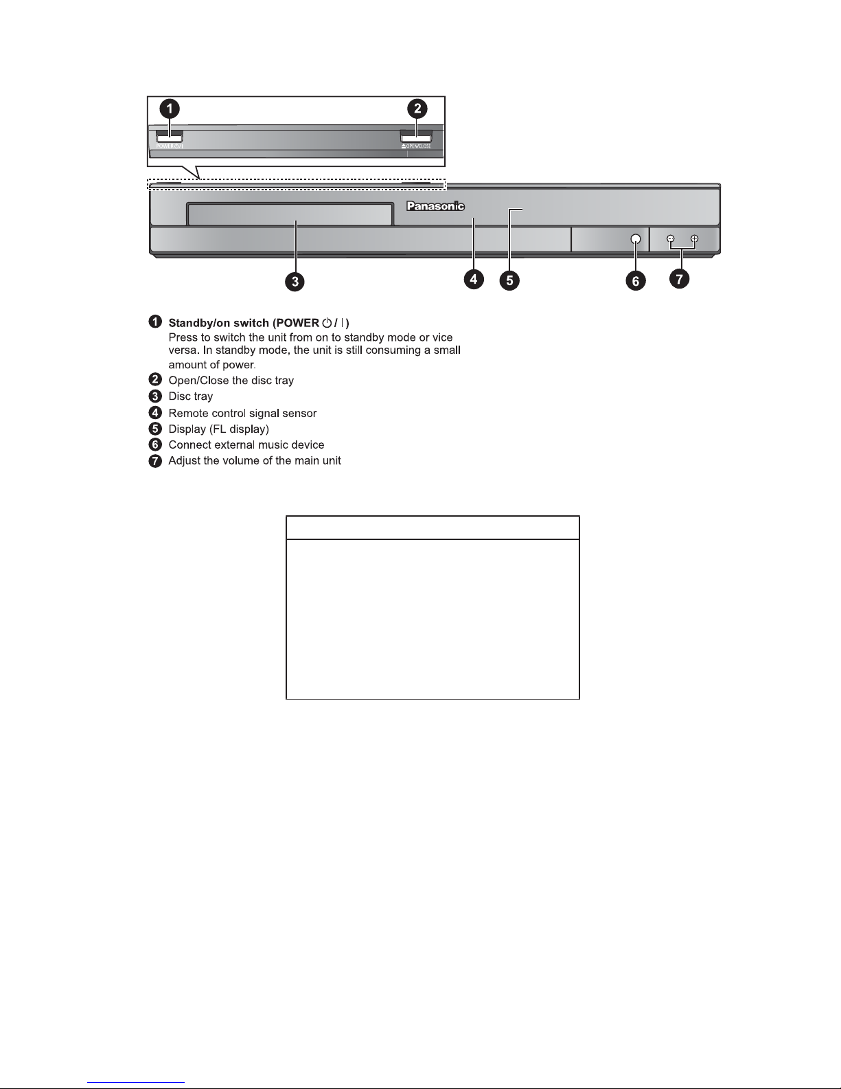
5.1. Remote Control and Main Unit Key Button Operations
15
5.2. Main Unit Key Button Operations
5.3. Power-Saving Features
MUSIC PORT
VOL
POWER-SAVING FEATURES
The main unit is designed to conserve its power
consumption and save energy.
Auto power-down function
The main unit will automatically switch to standby mode after
30 minutes of inactivity.
e.g.
– There is no audio signal from an external device.
– Disc playback is stopped/paused.
– The disc menu is displayed and play is not selected.
(This function may not work depending on the application
type of discs.)
g

16
5.4. Speaker Connection
17
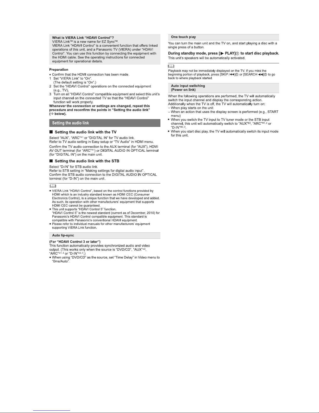
5.5. Linked Operations with the TV (VIERA LINK “HDAVI Control™”)
18
19
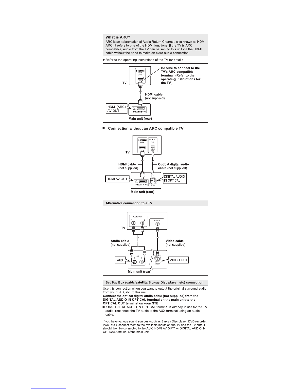
5.6. Connection with an ARC compatible TV
20
5.7. Disc Information
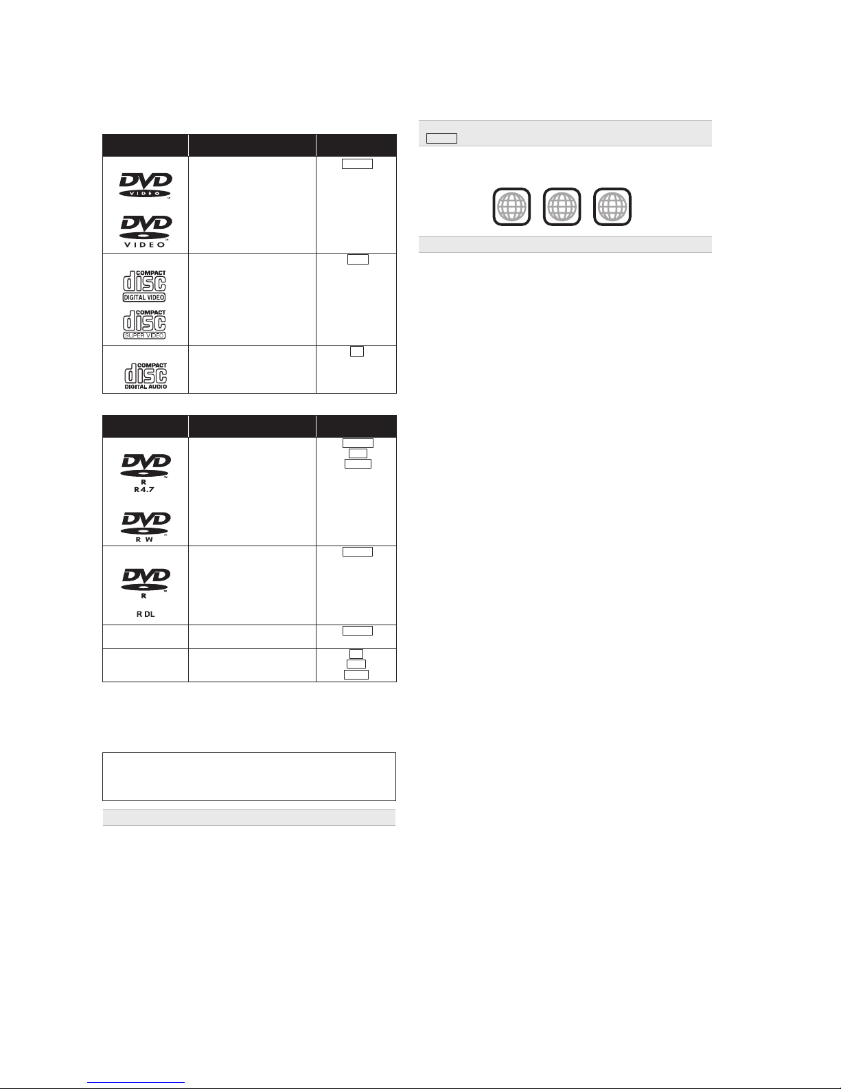
5.7.1. Discs that can be played
Commercial discs
Recorded discs
• Before playback, finalize the disc on the device it was recorded on.
• It may not be possible to play all the above-mentioned discs in some
cases due to the type of disc, the condition of the recording, the
recording method, or how the files were created.
• During playback of DTS source, there will be no sound from the
speakers.
Blu-ray Discs, HD DVD, AVCHD discs, DVD-RW version 1.0, DVD-Audio,
DVD-ROM, DVD-VR, CD-ROM, CDV, CD-G, SACD, DTS Music Discs,
WMA discs, DivX discs and Photo CD, DVD-RAM, and “Chaoji VCD”
available on the market including CVD, DVCD and SVCD that do not
conform to IEC62107.
Type of media/
Logo
Remarks Indicated as
DVD-Video High quality movie and
music discs
DVD-V
DVD-V
DVD-V
DVD-V
Video CD Music discs with video
Including SVCD
(Conforming to IEC62107)
VCD
CD Music discs
CD
CD
Type of media/
Logo
Formats Indicated as
DVD-R/RW • DVD-Video Format
• MP3 format
• JPEG format
MP3
MP3
JPEG
JPEG
DVD-R DL • DVD-Video Format
+ R/+ RW/+ RDL • VR (++ R/+ RW Video
Recording) Format
CD-R/RW • CD-DA format
• MP3 format
• JPEG format
Note about using a DualDisc
The digital audio content side of a DualDisc does not meet the technical
specifications of the Compact Disc Digital Audio (CD-DA) format so
playback may not be possible.
Discs that cannot be played
The player plays DVD-Video marked with labels containing the region
number “1” or “ALL”.
e.g.
• Do not attach labels or stickers to discs. This may cause disc warping,
rendering it unusable.
• Do not write on the label side with a ball-point pen or other writing
instrument.
• Do not use record cleaning sprays, benzine, thinner, liquids which
prevent static electricity, or any other solvent.
Do not use scratch-proof protectors or covers.
• Do not use the following discs:
– Discs with exposed adhesive from removed stickers or labels (rented
discs, etc.).
– Discs that are badly warped or cracked.
– Irregularly shaped discs, such as heart shapes.
Region number
Disc handling precautions
1 ALL
2
4
1
DVD-V
21
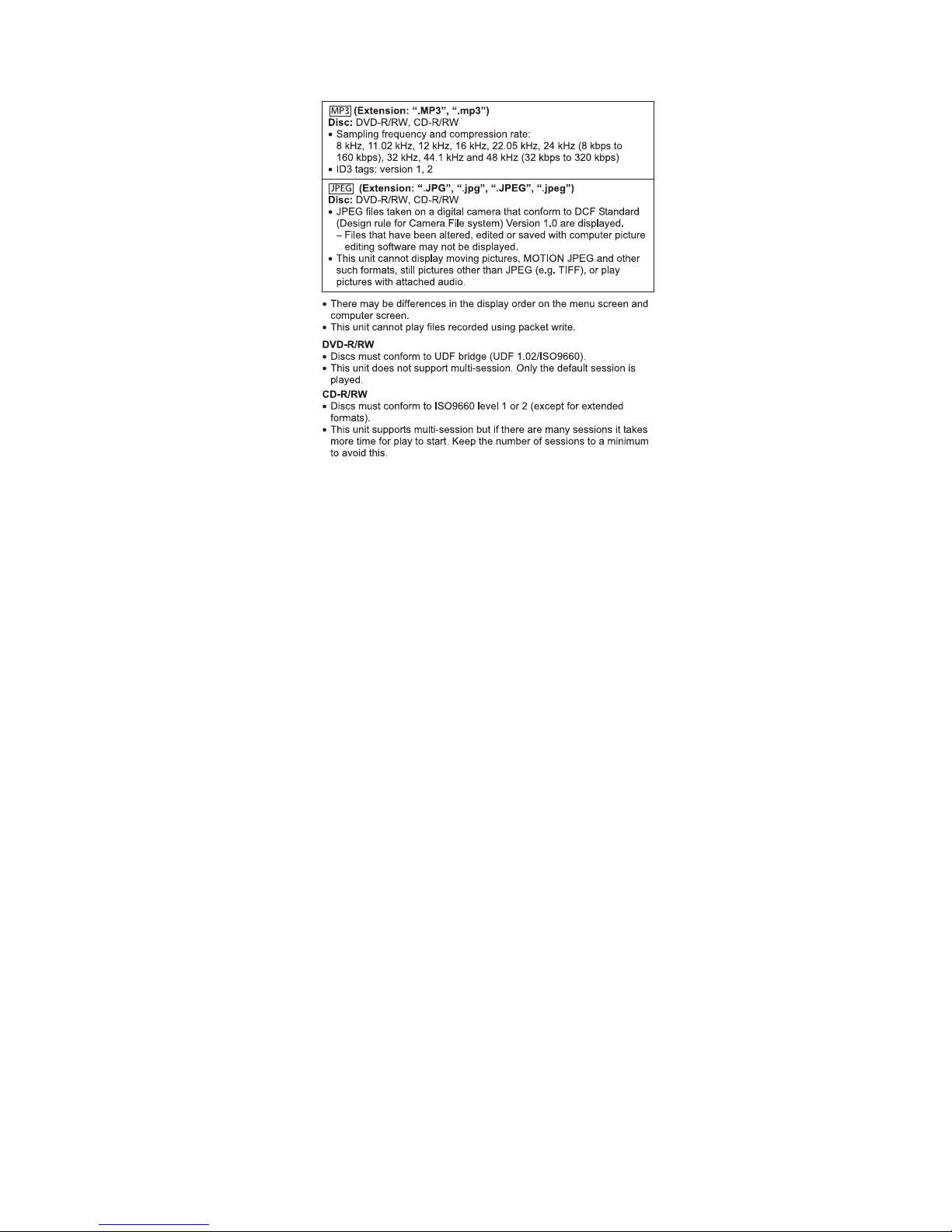
5.7.2. File Extension Type Support (MP3/JPEG)
22
6 Operating Instructions
6.1. Removing of disc during abnomality
6.1.1. Using main unit key buttons.
6.1.1.1. When the power can be turned off.
1. Turn off the power and press & hold [OPEN/CLOSE] button on main unit and [SKIP FWD] button on remote for 5 seconds
6.1.1.2. When the power cannot be turned off
1. Press & hold the [POWER] button to turn off the power forcibly, then press & hold [SKIP FWD] button on remote and [OPEN/
CLOSE] button on main unit for 5 seconds.
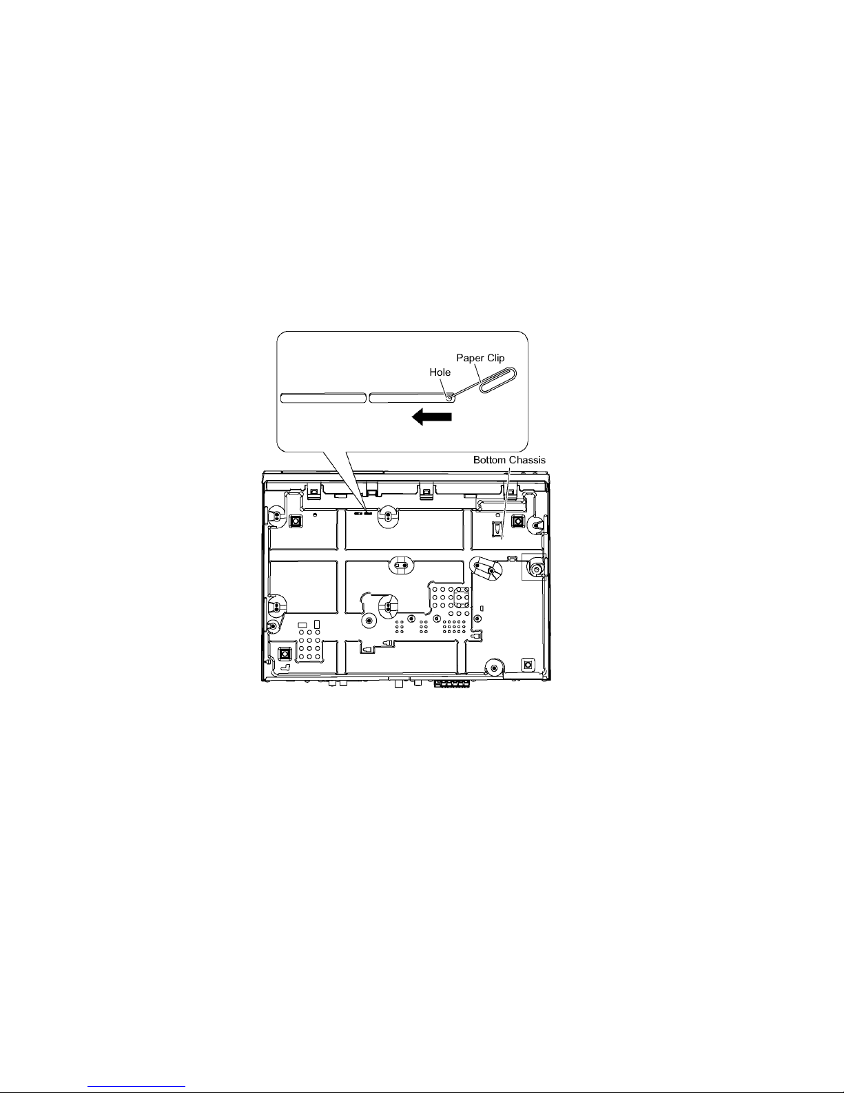
6.1.2. When the Forcible Disc Eject cannot be done.
1. Turn off the power and remove AC cord.
2. Insert Paper Clip into the hole on the bottom of unit and slide the Paper Clip on the direction of the arrow to eject tray slightly.
The tray will open automatically.
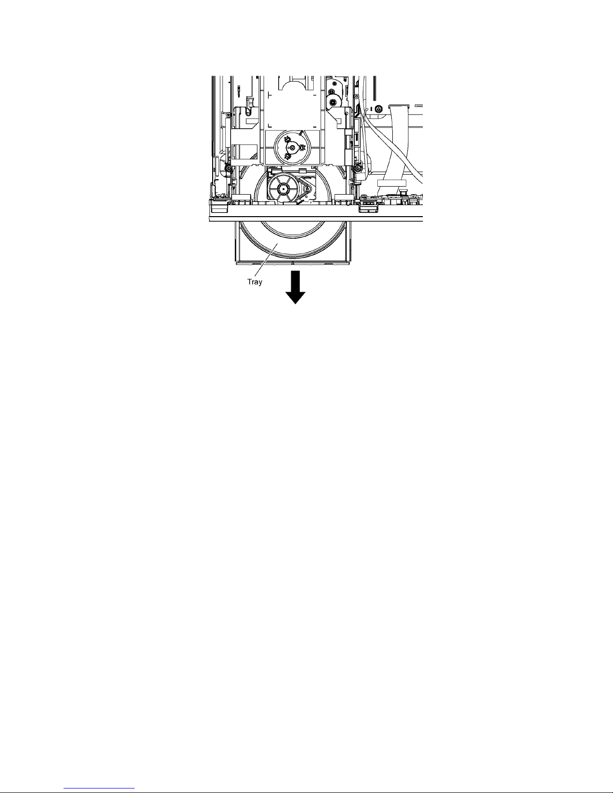
23
3. Gently pull out the tray.
4. Remove disc

24
7 Self-Diagnostic and Special Mode Setting
7.1. Cold-Start
Here is the procedure to carry out cold-start for initialize to shipping mode.
1. Unplug AC power cord
2. Press & hold [POWER] button
3. Plug AC power cord while [POWER] button being pressed
FL Display will show “_ _ _ _ _ _ _ _”
4. Release [POWER] button
7.2. Service Mode Table
By pressing various button combinations on the main unit and re mote control unit, yo u can activate the various service modes fo r
checking.
Special Note:
• Due to the limitations of the no. characters that can be shown on the FL Displa y, the “FL Display” button on the remote control
unit can be used to show the two display pages. (Display 1 / Display 2).
• Refer to Section 5.1 for the section on “Remote Control Key Buttons Operations”.
25
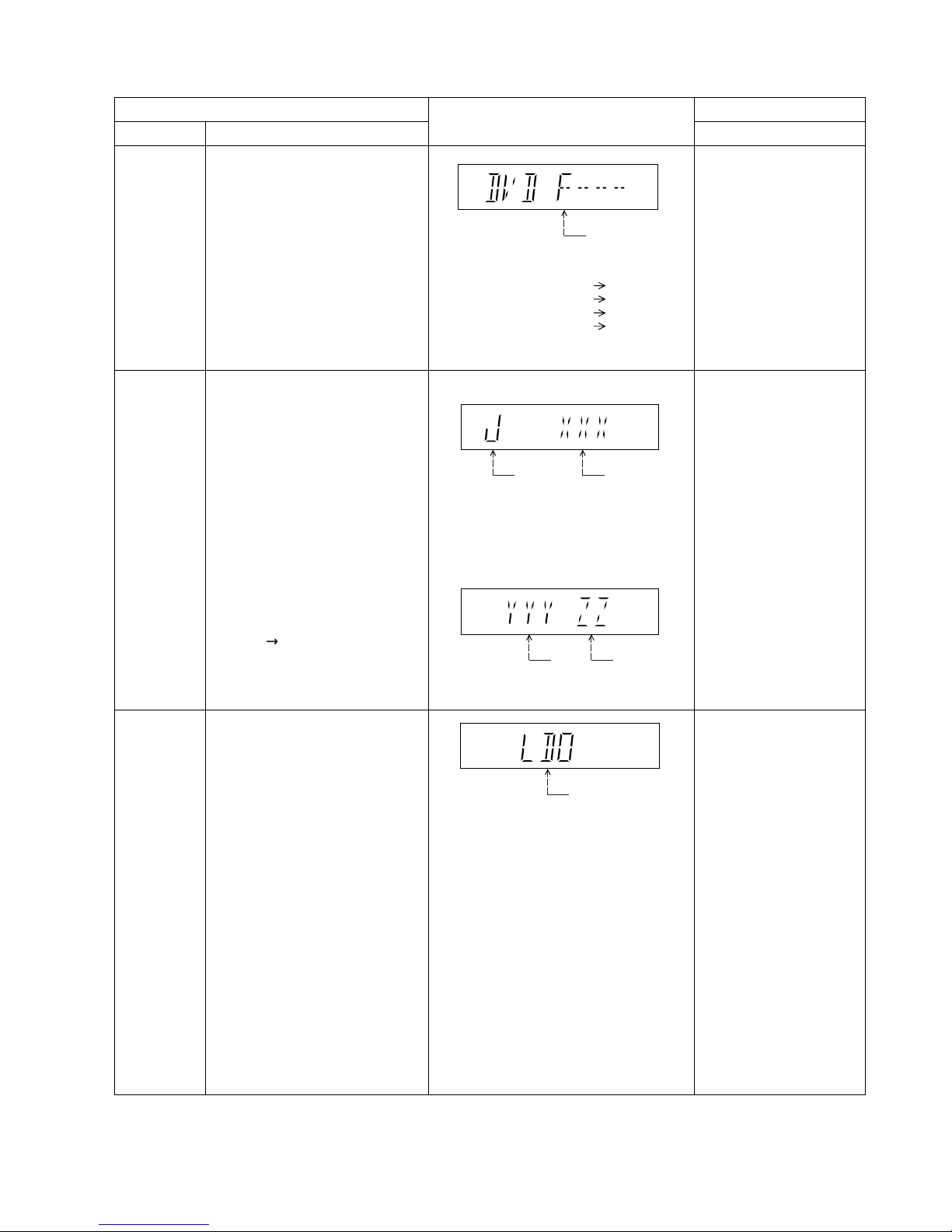
7.2.1. Service Mode Table 1 (For DVD)
Initial setting of
laser drive
current
Jitter check
Jitter check.
Jitter rate is measured and displayed.
Measurement is repeatedly done in
the cycle of one second. Read error
counter starts from zero upon mode
setting.
When target block data failed to be
read out, the counter advances by one
increment. When the failure is caused
by minor error, it may be corrected
when retried to enable successful
reading.
In this case, the counter advances by
one. When the error persists even
after retry, the counter may jump by
two or more.
FL Display sequence:
Display 1 2.
Jitter rate is shown in decimal notation to one
place of decimal.
Focus drive value is shown in hexadecimal
notation.
(Display 1)
Jitter rate
Jitter check
mode
(Display 2)
Lead
Error
Counter
Focus Drive
Value
Press [POWER] button to exit.
In STOP (with disc inside
tray) mode, press
[OPEN/CLOSE] button on
the main unit, and [5]
button on
the remote control unit.
Press [FL Display] on
remote control unit for next
page (FL Display).
Error code
check
Error code check
The latest error code stored in the
EEPROM IC is displayed.
Note: Refer to "(Section 7.4) Self
Diagnostic Function-Error Code" for
more detailed information on the error
codes.
Error code (play_err) is expressed in the
following convention.
Error code = 0 x DAXX is expressed: DVDnn U12
Error code = 0 x DBXX is expressed: DVDnn H12
Error code = 0 x DXXX is expressed: DVDnn F123
Error code = 0 x 0000 is expressed: DVDnn F--* "xx" denotes the error code
F / H / U
To exit, press [POWER]
button on main unit or
remote control.
In STOP (no disc) mode,
press [
OPEN/CLOSE
]
button on the main unit, and
[0] button on the remote
control unit. *With pointing of
cursor up and down on
display.
In STOP (no disc) mode,
press [OPEN/CLOSE]
button on the main unit,
and [PAUSE] button on the
remote control unit.
Initial setting of laser drive current.
The value denotes the current in decimal
notation.
Laser current
measurement
mode
FL Display
Key Operation
Front Key
Item
DescriptionMode Name
26
7.2.2. Service Mode Table 2 (For DVD)
FL Display
Key Operation
Front Key
Item
DescriptionMode Name
CD laser drive
current
measurement
In STOP (no disc) mode,
press [OPEN/CLOSE]
button on the main unit,
and [3] button on the
remote control unit.
DVD laser
drive current
measurement
CD laser current
measurement mode
(Display 1)
In STOP (no disc) mode,
press [OPEN/CLOSE]
button on the main unit,
and [FUNCTIONS] button
on the remote control unit.
To exit, press Power Off
Button on remote control.
To exit, press Power Off
Button on remote control.
The value denotes the current in decimal
notation.
DVD laser current
measurement mode
DVD laser drive current measurement.
For DVD laser drive current, refer to
Troubleshooting Guide (Section 8.2)
CD laser drive current measurement.
For CD laser drive current, refer to
Troubleshooting Guide (Section 8.2)
Region code display, TV broadcasting
system & the model no. information.
Note: Refer to Figure 7.1 for "Video
Design Information".
Region display
Display is automatically
clear after 5 seconds.
In STOP (no disc)
mode, press
[OPEN/CLOSE] button on
the main unit, and [6]
button on the remote
control unit.
N: no PAL / P: PAL
Model
No.
Information
N: NTSC / 6: PAL60
Region No.: 0-8

27
7.2.3. Service Mode Table 3 (For DVD)
FL Display
Key Operation
Front Key
Item
DescriptionMode Name
Initialization
Micro-processor
firmware version
display &
EEPROM
checksum
display.
Initialization.
User settings are cancelled and player
is initialized to factory setting.
It is necessary when after replacement
of Micro-processor IC, FLASH ROM IC
(IC8651), IC200 & Main P.C.B.
Micro-processor firmware version
display & EEPROM checksum display.
EEPROM checksum is only available
due to existence of EEPROM IC.
Note: Condition 1/2/3 shows the state
of EEPROM IC.
FL Display sequence:
Display 1 2 3.
In STOP (no disc)
mode, press
[OPEN/CLOSE] button on
the main unit, and [ 10]
button on the remote
control unit.
Cancelled automatically
5 seconds later.
In STOP (no disc)
mode, press
[OPEN/CLOSE] button on
the main unit, and [7]
button on the remote
control unit.
Press [FL Display] button on
remote control unit for next
page. (FL Display)
(Display 2)
If the version of the EEPROM does not match,
[NG] is displayed.
(Condition 1)
(a) If there is NO EEPROM header string
OR
(b) If there is no EEPROM (no data is received
by Micro-processor), [NO] is displayed.
(Condition 2)
Opecon
Version
EEPROM
Checksum
(If applicable,
refer below.)
(Display 3)
(Display 1)
(Condition 3)
If the EEPROM version matches, checksum
[YYYY] is displayed.
28
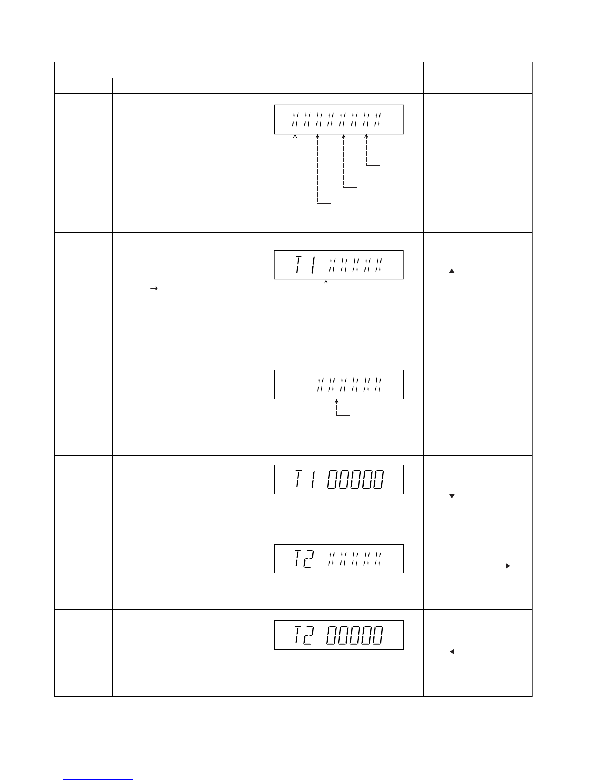
7.2.4. Service Mode Table 4 (For DVD)
FL Display
Key Operation
Front Key
Item
DescriptionMode Name
DVD
firmware
version display
Cancelled automatically
5 seconds later.
In STOP (no disc)
mode, press
[OPEN/CLOSE] button on
the main unit, and [8]
button on the remote
control unit.
DVD firmware version is displayed on
the FL Display.
The firmware version can be updated
using recovery disc.
Note: It is necessary to check for
firmware version before carrying out
the version up using the disc.
Destination
System
controller
version
System controller
generation
Region No.: 0-8
Timer 1 check
DVD laser usage time
(Display 1)
Shown to the above is DVD laser usage
time, and to the below is CD laser usage
time.
Time is shown in 5 digits of decimal notation
in a unit of 10 hours.
"00000" will follow "99999". (DVD laser)
(Display 2)
CD laser usage time
Time is shown in 6 digits of decimal notation
in a unit of 10 hours.
"000000" will follow "999999". (CD laser)
Press [FL Display] button for
next page of FL Display.
Cancelled automatically
5 seconds later.
In STOP (no disc) mode,
press [OPEN/CLOSE]
button on the main unit,
and [ ] button on the
remote control unit.
Timer 1 reset
Timer 2 check
Timer 2 reset
Timer 1 check
Laser operation timer is measured
separately for DVD laser and CD laser.
FL Display sequence:
Display 1 2.
Timer 1 reset
Laser operation timer of both DVD
laser and CD laser is reset all at once.
Timer 2 check
Spindle motor operation timer
Timer 2 reset
Spindle motor operation timer
Time is shown in 5 digits of decimal notation
in a unit of 10 hours.
It will clear to "00000" upon reset.
Time is shown in 5 digits of decimal notation in
a unit of 1 hour.
"00000" will follow "99999".
Time is shown in 5 digits of decimal notation in
a unit of 1 hour.
It will be cleared to "00000" upon activating
this.
Cancelled automatically
5 seconds later
While displaying Timer 1
data, press [OPEN/CLOSE]
button on the main unit,
and [ ] button on the
remote control unit.
In STOP (no disc) mode,
press [OPEN/CLOSE] button
on the main unit, and [ ]
button on the remote control
unit.
Cancelled automatically
5 seconds later.
Cancelled automatically
5 seconds later
While displaying Timer 2
data, press [OPEN/CLOSE]
button on the main unit,
and [ ] button on the remote
control unit.
29
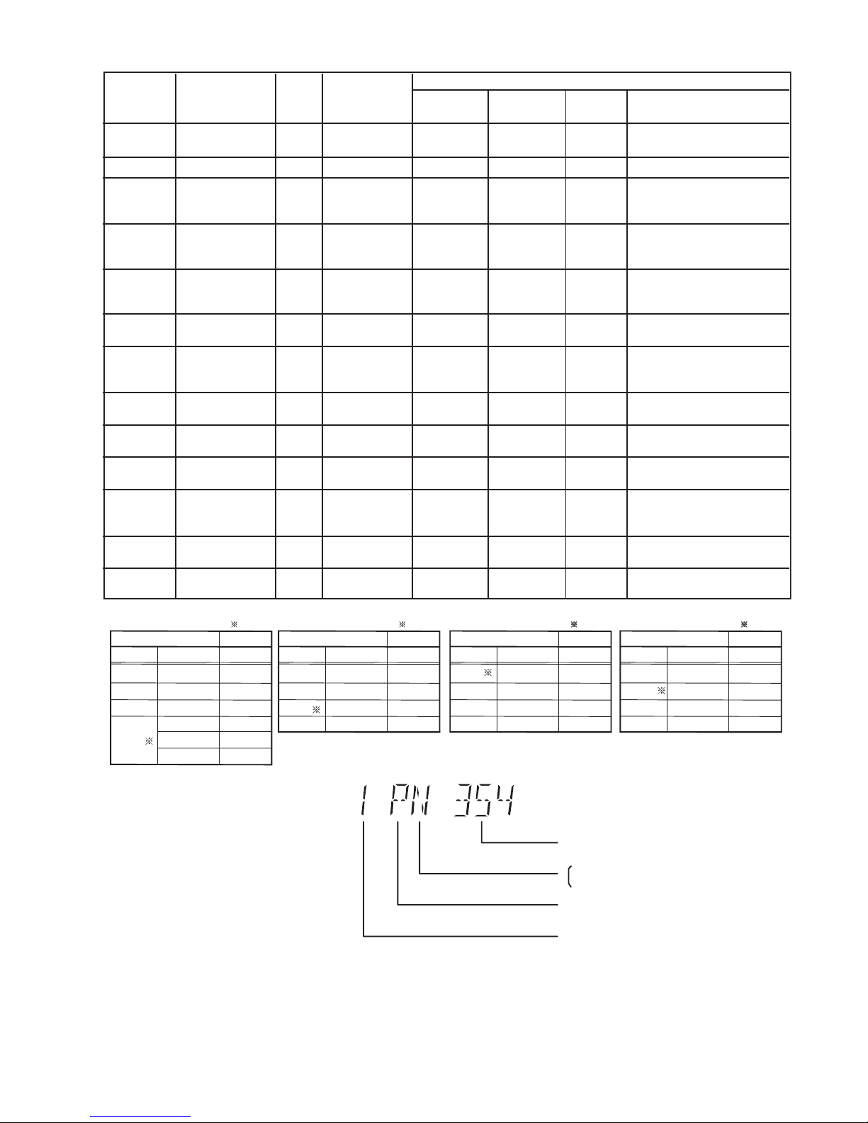
Figure 7.1 Video Design Information
English (NA), Spanish (NA),
Canadian, French
Japanese, English
English (EU), French, German,
Spanish (EU), Polish, Russian,
Czech, Hungarian
English (EU), French, German,
Italian, Spanish (EU), Polish,
Swedish, Dutch
English (NA), French, German,
Spanish (EU), Polish, Russian,
Czech, Hungarian
GA, GD
GT, GJ
English (NA), Traditional
Chinese
English (EU), French, German,
Italian, Spanish (EU), Polish,
Swedish, Dutch
English (NA), Spanish (Panama),
French, Brazilian Portuguese
English (EU), French, German,
Spanish (EU), Polish, Russian,
Czech, Hungarian
GN
EE
PH, PU,
PR
EP
P, PC, PX,
PP
GC, GS
EB, EG,
2
5
4
4
2
2
1
2
3
DVD
Region
Code
NTSC
PAL / NTSC
SECAM
NTSC
PAL
PAL
PAL
NTSC
PAL
TV Broadcasting
System
NTSC (*D)
NTSC (*D)
PAL ( *C )
PAL ( *C )
PAL ( *C )
PAL ( *C )
Auto (*B)
Auto (*B)
PAL ( *C )
Selected
TV System
2PN
4PN
4PN
5PP
3PN
1PN
2PP
2PP
2PP
4PP
Region Display
(Default)
Product
Series
Code
Japan
South East Asia,
Korea, Taiwan
New Zealand,
Australia
South/Centrial
America, Argentina
CIS
Poland, E.Europe
USA, Canada,
US Militry
UK, Germany,
W.Europe
Middle East,
Africa, S.E.A
Country
OSD Language
OSD
Default
English
English
English
English
English (NA), Traditional
Chinese
GW 5 PAL PAL ( *C) 5PPIndia
English
English
English
English
English
GK English (NA), Simplified Chinese6 PAL 6PNChina
Simplified
Chinese
Japanese
English (NA), Spanish (Panama),
French, Brazilian Portuguese
PN 4 NTSC
Central &
S.America, Brazil
Spanish
NTSC (*D) 4PN
English (NA), Spanish (Panama),
French, Brazilian Portuguese
PB 4 NTSC
Central &
S.America, Brazil
Portuguese
AUTO2 (*A)
AUTO2 (*A)
(blank)
Explanation of Display
Individual Model Code
Can play PAL disc
Region code
N: If NTSC disc is played, NTSC output.
6: If NTSC disc is played, PAL60 output.
Auto2 (*A)
Auto2
TV sys
Source
Output
Select TV System
PAL -- - -
-- --
-- --
NTSC
NTSC
PAL DVD-V
PAL VCD
PAL
NTSC
NTSC
Auto
No
= default
Wallpaper = NTSC
Auto2 (*B)
Auto2
TV sys
Source
Output
Select TV System
PAL
-- --
NTSC
PAL / NTSC
PAL / NTSC
PAL / NTSC
same as source
Auto
Yes
= default
Wallpaper = NTSC
PAL
NTSC
PAL (*C)
Auto2
TV sys
Source
Output
Select TV System
PAL
-- --
NTSC
PAL / NTSC
PAL / NTSC
PAL / NTSC
same as source
Auto
Yes
= default
Wallpaper = PAL
PAL
NTSC
NTSC (*D)
Auto2
TV sys
Source
Output
Select TV System
PAL
-- --
-- --
-- --
NTSC
PAL / NTSC
Auto
Yes
= default
Wallpaper = NTSC
NTSC
30
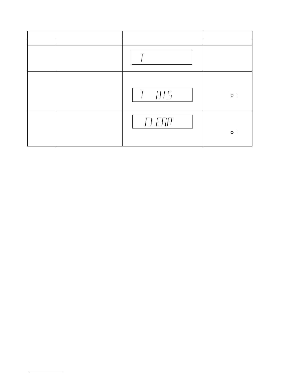
7.3. Self-Diagnostic Mode
Delete Error
Codes
Error code
information
System will perform a check on
any unusual/error code from the
memory
Error code will display
Example:
Self-Diagnostic
Mode
To enter into self-diagnostic checking
Press & hold
[OPEN/CLOSE] on main
unit, follow by [4] then [9] on
remote control. (When no
disc in mechanism)
System will clear all of the contents
of unusual/error code from the
memory
FL Display
Key Operation
Front Key
Item
DescriptionMode Name
In self-diagnostic mode,
press [STOP] on remote
control.
To exist, press [ / ]
on main unit or remote
control.
In self-diagnostic mode,
press [CANCEL] on remote
control.
To exist, press [ / ]
on main unit or remote
control.
 Loading...