

Page 1
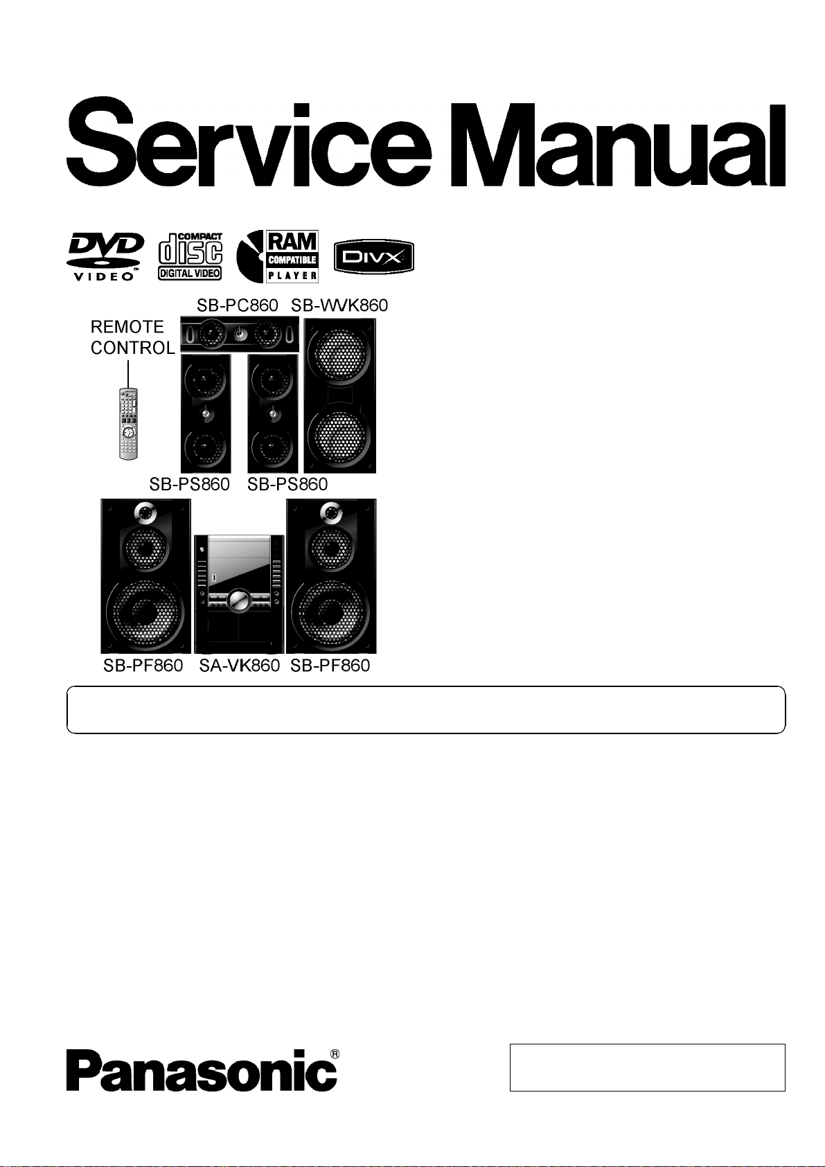
DVD Stereo System
SA-VK860GC
SA-VK860GCS
SA-VK860GS
Colour
(K)... Black Type
ORDER NO. MD0707030CE
Notes: This model’s DVD changer mechanism unit is CRS1D. Please refer to the original Service Manual
(Order No. MD0603065A3) for this mechanism.
Specifications
Q
Q AMPLIFIER SECTION
QQ
RMS Output Power: Dolby Digital Mode
OFront Ch 110 W per channel (3 Ω), 1 kHz,
10% THD
OSurround Ch 110 W per channel (3 Ω), 1 kHz,
10% THD
OCenter Ch 110 W per channel (3 Ω), 1 kHz,
10% THD
OSubwoofer Ch 110 W per channel (3 Ω), 100 Hz,
10% THD
OTotal RMS Dolby Digital mode power
660 W
PMPO output power 7000 W
Q
Q FM/AM TUNER, TERMINALS SECTION
QQ
Preset station FM 20 stations
AM 15 stations
Frequency Modulation (FM)
OFrequency range 87.50 to 108.00 MHz (50 kHz
OSensitivity 4.0 µV (IHF)
OS/N 26 dB 2.2 µV
OAntenna terminals 75 Ω (unbalanced)
Amplitude Modulation (AM)
OFrequency range 522 to 1629 kHz (9 kHz step)
520 to 1630 kHz (10 kHz step)
© 2007 Matsushita Electric Industrial Co. Ltd.. All
rights reserved. Unauthorized copying and
distribution is a violation of law.
step)
Page 2

r
SA-VK860GC / SA-VK860GCS / SA-VK860GS
AM Sensitivity S/N 20 dB at 999 kHz
1000 µV/m
Music Port input jack
OSensitivity 100 mV, 4.7 kΩ
OTerminal Stereo, 3.5 mm jack
Phone jack
OTerminal Stereo, 3.5 mm jack
Mic jack
OSensitivity 0.7 mV, 600 Ω
OTerminal Mono, 6.3 mm jack (2 system)
AUX
OSensitivity 2V,8kΩ
OTerminal Stereo, RCA jack
USB Port
OUSB standard USB 2.0 full speed
OMedia file format support MP3 (*.mp3)
WMA (*.wma)
JPEG (*.jpg, *.jpeg)
MPEG4 (*.asf)
OUSB device file system FAT12, FAT16, FAT32
OUSB port power 500 mA (Max)
Q
Q CASSETTE DECK SECTION
QQ
OType 1 way, Auto Reverse
OTrack system 4-T rack, 2 Cha nne l
Heads
ORecord/Playback Solid permalloy head
OErasure Double gap ferrite head
Motor DC servo moto
Recording system AC bias 100 kHz
Erasing system AC erase 100 kHz
Tape speed 4.8 cm/s
Overall frequency response (+3, -6 dB) at DECK OUT
ONormal 35 Hz to 14 kHz
S/N ratio 50 dB (A weighted)
Wow and flutter 0.18% (WRMS)
Fast forward and rewind time
Approx. 120 seconds with C-60 cassette tape
Q
Q VIDEO SECTION
QQ
Video system PAL625/50, PAL525/60, NTSC
Composite video output
OOutput level 1 Vp-p (75 Ω)
OTerminal Pinjack(1system)
Component video output
[NTSC: 480p/480i, PAL: 576p/576i]
OY output level 1 Vp-p (75 Ω)
OPBoutput level 0.7Vp-p(75Ω)
OPRoutput level 0.7Vp-p(75Ω)
OTerminal
Pin jack (Y: green, PB:blue,PR:red)(1system)
Q
Q DISC SECTION
QQ
Disc played [8 cm or 12 cm]
(1) DVD (DVD-Video, DivX
(2) DVD-RAM (DVD-VR, JPEG
#7
)
#6, #7
)
#4,#7
,MP3
#2,#7
, MPEG4
#5,#7
, DivX
#6,
(3) DVD-R (DVD-Video, DVD-VR, JPEG
#6,#7
DivX
)
# 4, #7,
MP3
#2,#7
, MPEG4
#5,#7
(4) DVD-R DL (DVD-Video, DVD-VR)
(5) DVD-RW (DVD-Video, DVD-VR, JPEG
#6,#7
#7
, DivX
)
#4,#7
,MP3
#2,#7
, MPEG4
#5,
(6) +R/+RW (Video)
(7) +R DL (Video)
(8) CD,CD-R/RW [CD-DA, Video CD, SVCD#1,MP3
JPEG
#4,#7
, MPEG4
#5,#7
, DivX
#6,#7
, HighMAT Level 2 (Audio and
#2,#7
,WMA
#3,#7
Image)]
#1
Conforming to IEC62107
#2
MPEG-1 Layer 3, MPEG-2 Layer 3
#3
Windows Media Audio Ver.9.0 L3
Not compatible with Multiple Bit Rate (MBR)
#4
Exif Ver 2.1 JPEG Baseline files
Picture resolution: between 160 x 120 and 6144 x 4096 pixels
(Sub sampling is 4:0:0, 4:2:0, 4:2:2 or 4:4:4). Extremely long and
narrow pictures may not be displayed.
#5
MPEG4 data recorded with the Panasonic SD multi cameras or
DVD video recorders.
Conforming to SD VIDEO specifications (ASF standard) / MPEG4
(Simple Profile) video system/ G.726 audio system.
#6
Plays all versions of DivX®video (including DivX®6) with standard
playback of DivX
®
media files. Certified to the DivX Stereo System
Profile.
#7
The total combined maximum number of recognizable audio,
picture and video contents and groups: 4000 audio, picture and video
contents and 400 groups.
Pick up
Wavelength
OCD 785 nm
ODVD 662 nm
Laser power
OCD CLASS 1M
ODVD CLASS 1
Audio output (Disc)
ONumber of channels (FL,FR,C,SL,SR,SW)5.1ch
Audio performance (measurement at: Rec out terminal)
OFrequency response (CD-Audio) 4Hzto20kHz
Q
Q GENERAL
QQ
Power supply
OGC area: AC 220 to 240 V, 50/60 Hz
OGCS/GS areas: AC 110 to 127V/ 220 to 240 V,
50/60 Hz
Power consumption 290 W
Power consumption in standby mode
0.9 W (approximate)
Dimensions (W x H x D) 250 x 330 x 334.6 mm
Mass 5.5 kg
Operating temperature range +5°C to +35°C
Operating humidity range 5% to 90% RH (no condensation)
Notes:
1. Specifications are subject to change without notice.
Mass and dimensions are approximate.
2. Total harmonic distortion is measured by the digital spectrum
analyzer.
,
,
2
Page 3
Q
Q SYSTEM
QQ
SA-VK860GC / SA-VK860GCS / SA-VK860GS
Refer to the respective original service manuals for *1, *2, *3, *4.
This model uses CRS1D mechanism (DVD/CD changer mechanism).
You can refer to the original service manual for information on this
mechanism.
3
Page 4

SA-VK860GC / SA-VK860GCS / SA-VK860GS
CONTENTS
Page Page
1 Safety Precautions 6
1.1. General Guidelines
1.2. Safety Precaution for AC Power Supply Cord (For GS
only)
1.3. Before Use (For GCS/GS only)
1.4. Before Repair and Adjustment
1.5. Protection Circuitry
1.6. Safety Parts Information
2 Prevention of Electrostatic Discharge (ESD) to
Electrostatically Sensitive (ES) Devices
3 Precaution of Laser Diode
4 About Lead Free Solder (PbF)
4.1. Service caution based on legal restrictions
5 Handling Precautions for Traverse Unit
5.1. Handling Optical Pickup in Traverse Unit
5.2. Replacing Precautions for Optical Pickup Unit
5.3. Grounding for Preventing Electrostatic Destruction
6 Accessories
7 Operation Procedures
7.1. Main Unit Key Buttons Operations
7.2. Remote Control Key Buttons Operations
7.3. Portable Audio Equipment Connection & Operation
7.4. USB Connection & Operation
7.5. About DivX VOD Content
7.6. Disc Information
8 DVD/CD Changer Mechanism Unit
8.1. CRS1D Mechanism Overview
9 Self Diagnosis and Special Mode Setting
9.1. Service Mode Summary Table
9.2. Service Mode Table (For DVD)
9.3. Service Mode Table (For Inspection)
9.4. DVD Self Diagnostic Function-Error Code
9.5. Sales Demonstration Lock Function
9.6. Service Precautions
10 Assem bling and Disassembl ing
10.1. Disassembly Flow Chart
10.2. Main Components and P.C.B. Locations
10.3. Disassembly of Top Cabinet
10.4. Disassembly of the DVD/CD Changer Mechanism Unit
10.5. Disassembly of DVD Module P.C.B.
10.6. Disassembly of USB Relay P.C.B.
10.7. Disassembly of Rear Panel
10.8. Disassembly of Main P.C.B.
10.9. Replacement of Regulator IC (IC2810)
10.10. Disassembly of Front Panel
10.11. Disassembly of Mic P.C.B.
10.12. Disassembly of Panel P.C.B
10.13. Disassembly of Tact Switch P.C.B
10.14. Disassembly of USB P.C.B
10.15. Replacement of CD Lid
10.16. Disassembly of Deck Mechanism Unit
10
11
11
12
12
12
12
14
15
15
16
17
18
19
20
22
22
25
25
26
33
38
45
45
47
49
50
51
51
52
52
53
53
54
54
56
56
56
57
57
57
6
7
7
7
7
8
9
10.17. Replacement of Cassette Lid
10.18. Disassembly of Deck P.C.B
10.19. Disassembly of D-Amp P.C.B. & Speaker P.C.B.
10.20. Replacement of Digital Amp IC (IC5100)
10.21. Disassembly of SMPS P.C.B.
10.22. Replacement of Switch Regulator IC (IC5701)
10.23. Replacement of Regulator Diode (D5904/D5905)
10.24. Replacement of Regulator Diode (D5702)
10.25. Disassembly of Traverse Unit
10.26. Disassembly of Deck Mechanism
10.27. Rectification for Tape Jam Problem
11 Service Positi on
11.1. Checking & Repairing Main P.C.B.
11.2. Checking & Repairing Speaker P.C.B.
11.3. Checking & Repairing Panel P.C.B.
11.4. Checking & Repairing Deck P.C.B.
11.5. Checking & Repairing Deck Mechanism P.C.B.
11.6. Checking & Repairing Mic P.C.B.
11.7. Checking & Repairing DVD Module P.C.B.
11.8. Checking & Repairing D-Amp P.C.B.
11.9. Checking & Repairing SMPS P.C.B.
12 Adjustment Procedures
12.1. Cassette Deck Section
12.2. Tuner section
12.3. Alignment Points
13 Illustration of ICs, Transistors and Diodes
14 Vol tage and Waveform Chart
14.1. DVD Module P.C.B.
14.2. Main P.C.B.
14.3. Panel P.C.B.
14.4. Deck/Deck Mechanism & Mic P.C.B.
14.5. D-Amp P.C.B.
14.6. SMPS P.C.B.
14.7. Waveform Chart
15 Wiring Connection Diagra m
16 Block Diagra m
16.1. System Control
16.2. DVD (Servo)
16.3. DVD (Audio)
16.4. DVD (Video)
16.5. Deck
16.6. Audio
16.7. Audio Digital Amp
16.8. Power
17 Schem atic Diagra m Notes
18 Schematic Diagram
18.1. DVD Module Circuit
18.2. Main Circuit
18.3. Panel Circuit
18.4. Tact Switch/Mic/Deck Mechanism/USB Relay/USB Circuit
58
58
59
59
60
60
61
61
62
63
66
68
68
68
68
69
69
69
70
70
72
73
73
74
74
75
76
76
77
79
79
80
80
81
83
85
85
86
87
88
89
90
91
92
93
95
95
99
103
104
4
Page 5

SA-VK860GC / SA-VK860GCS / SA-VK860GS
18.5. Deck Circuit 105
18.6. D-Amp Circuit
18.7. SMPS Circuit
18.8. Speaker/Optical Pickup Unit Circuit
19 Prin ted Ci rcui t Board
19.1. DVD Module P.C.B.
19.2. Main P.C.B.
19.3. Panel/USB Relay/USB P.C.B.
19.4. Tact Switch/Mic/Deck/Deck Mechanism P.C.B.
19.5. D-Amp/Speaker P.C.B.
19.6. SMPS P.C.B.
20 Basic Troubleshooting Guide
106
108
112
115
115
116
117
118
119
120
123
20.1. Basic Troubleshooting Guide for Traverse Unit (DVD
Module P.C.B)
21 Terminal Function of IC
124
21.1. IC2600 (C2CBYY000470): System Control IC
21.2. IC6701 (C0HBB0000064): FL Driver IC
22 Expl od ed View s
22.1. Cabinet Parts Location
22.2. Deck Mechanism Unit Parts Location (RAA4901-S)
22.3. Packaging (SF-VK860)
23 Repl acement Parts Li st
23.1. Component Parts List
24 Schem atic Diagra m for printing w ith letter size
123
124
124
126
127
129
131
132
133
149
5
Page 6
SA-VK860GC / SA-VK860GCS / SA-VK860GS
1 Safety Precautions
1.1. General Guidelines
1. When servicing, observe the original lead dress. If a short circuit is found, replace all parts which have been overheated or
damaged by the short circuit.
2. After servicing, see to it that all the protective devices such as insulation barriers, insulation papers shields are properly
installed.
3. After servicing, make the following leakage current checks to prevent the customer from being exposed to shock hazards.
1.1.1. Leakage Current Cold Check
1. Unplug the AC cord and connect a jumper between the two prongs on the plug.
2. Measure the resistance value, with an ohmmeter, between the jumpered AC plug and each exposed metallic cabinet part on
the equipment such as screwheads, connectors, control shafts, etc. When the exposed metallic part has a return path to the
chassis, the reading should be between 1 MΩ and 5.2 MΩ.
When the exposed metal does not have a return path to the chassis, the reading must be
.
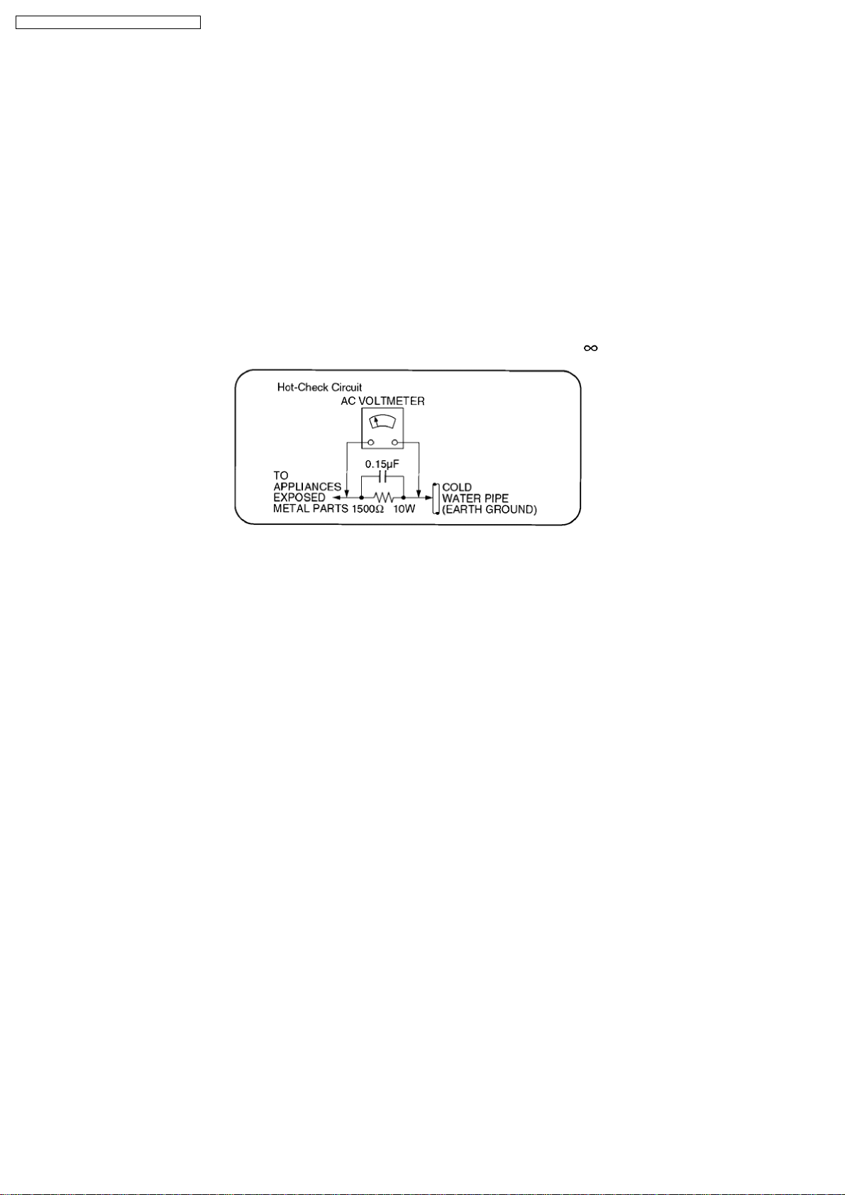
Figure 1
1.1.2. Leakage Current Hot Check
1. Plug the AC cord directly into the AC outlet. Do not use an isolation transformer for this check.
2. Connect a 1.5 kΩ, 10 watts resistor, in parallel with a 0.15 µF capacitor, between each exposed metallic part on the set and a
good earth ground such as a water pipe, as shown in Figure 1.
3. Use an AC voltmeter, with 1000 ohms/volt or more sensitivity, to measure the potential across the resistor.
4. Check each exposed metallic part, and measure the voltage at each point.
5. Reverse the AC plug in the AC outlet and repeat each of the above measurements.
6. The potential at any point should not exceed 0.75 volts RMS. A leakage current tester (Simpson Model 229 or equivalent) may
be used to make the hot checks, leakage current must not exceed 1/2 milliamp. In case a measurement is out of the limits
specified, there is a possibility of a shock hazard, and the equipment should be repaired and rechecked before it is returned to
the customer.
6
Page 7
SA-VK860GC / SA-VK860GCS / SA-VK860GS
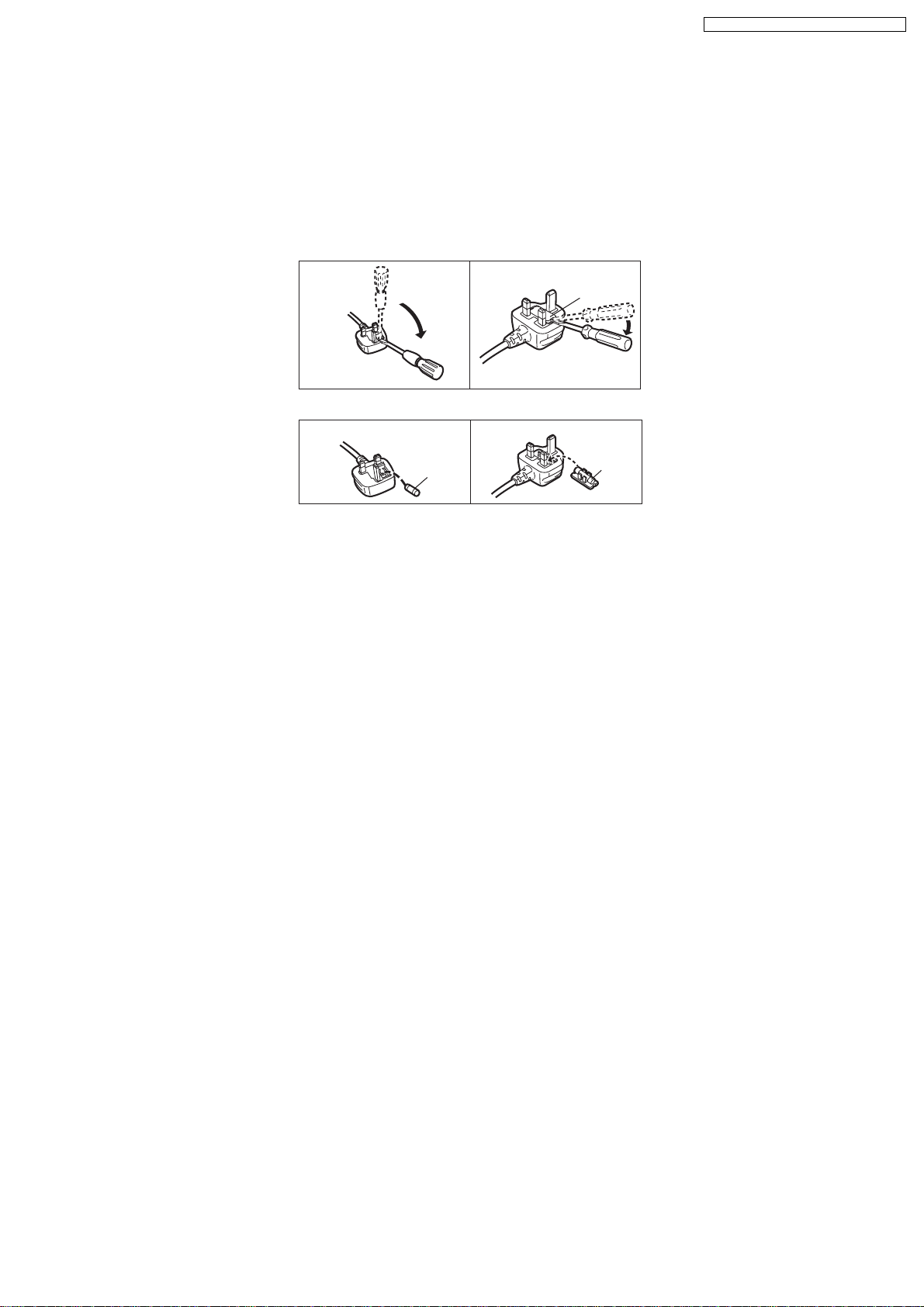
1.2. Safety Precaution for AC Power Supply Cord (For GS only)
Before use
Remove the connector cover.
How to replace the fuse
The location of the fuse differs according to the type of AC
power plug (fi gures A and B). Confi rm the AC power plug fi tted
and follow the instructions below.
Illustrations may differ from actual AC power plug.
1. Open the fuse cover with a screwdriver.
Figure A Figure B
Fuse cover
2. Replace the fuse and close or attach the fuse cover.
Figure A Figure B
Fuse
(5 ampere)
Fuse
(5 ampere)
1.3. Before Use (For GCS/GS only)
Be sure to disconnect the AC Power Supply Cord before adjusting the voltage selector.
Use a minus (-) screwdriver to set the voltage selector (on the rear panel) to the voltage setting for the area in which the unit will
be used. (If the power supply in your area is 110 V or 127 V, set to the “110 V~127 V” position.)
Note that this unit will be seriously damaged if this setting is not made correctly. (There is no voltage selector for some countries,
the correct voltage is already set.)
1.4. Before Repair and Adjustment
Disconnect AC power, discharge Power Supply Capacitors C2254, C2256, C2288, C2289, C2632, C2721, C2725, C2811, C2815,
C2817, C5512, C5513, C5514, C5711 (Not applicable for GC), C5712, C5713, C5715, C5790 (Not applicable for GC), C5805,
C5806, C5807, C5914, C5916, C5917, C5929, C5930, C5971 (Not applicable for GC), C5977 through a 10Ω,1Wresistorto
ground.
DO NOT SHORT-CIRCUIT DIRECTLY (with a screwdriver blade, for instance), as this may destroy solid state devices.
After repairs are completed, restore power gradually using a variac, to avoid overcurrent.
Current consumption at AC 110~127 V, 60 Hz in NO SIGNAL (Volume min, at CD mode) should be ~750 mA. [For GCS/GS only]
Current consumption at AC 220~240 V, 50 Hz in NO SIGNAL (Volume min, at CD mode) should be ~500 mA.
1.5. Protection Circuitry
The protection circuitry may have operated if either of the following conditions are noticed:
•
• No sound is heard when the power is turned on.
• •
•
• Sound stops during a performance.
• •
The function of this circuitry is to prevent circuitry damage if, for example, the positive and negative speaker connection wires are
“shorted”, or if speaker systems with an impedance less than the indicated rated impedance of the amplifier are used.
If this occurs, follow the procedure outlines below:
1. Turn off the power.
2. Determine the cause of the problem and correct it.
3. Turn on the power once again after one minute.
Note :
When the protection circuitry functions, the unit will not operate unless the power is first turned off and then on again.
7
Page 8

SA-VK860GC / SA-VK860GCS / SA-VK860GS
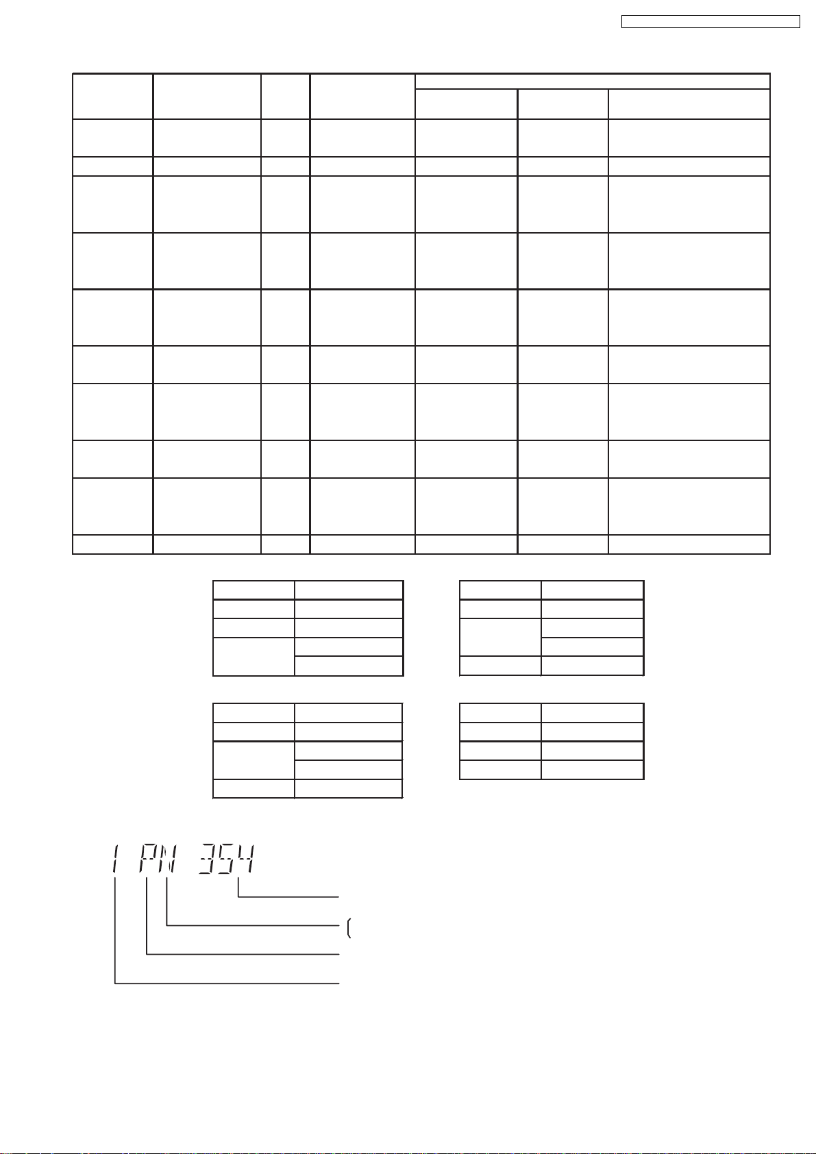
1.6. Safety Parts Information
Safety Parts List:
There are special components used in this equipment which are important for safety.
These parts are marked by
should be replaced with manufacturer’s specified parts to prevent shock, fire or other hazards. Do not modify the original design
without permission of manufacturer.
Ref. No. Part No. Part Name & Description Remarks
360 RAE2023Z-S TRAVERSE UNIT [M]
PC5703 B3PBA0000402 PHOTO COUPLER [M]
PC5801 B3PBA0000402 PHOTO COUPLER [M]
PC5805 B3PBA0000402 PHOTO COUPLER [M]
PC5901 B3PBA0000402 PHOTO COUPLER [M]
DZ5001 ERZV10V511CS ZENER [M]
TH5701 D4CAC8R00002 THERMISTOR [M]
TH5750 D4CC11040013 THERMISTOR [M]
TH5970 D4CAC8R00002 THERMISTOR [M] GCS/GS
L5001 ELF21N024A LINE CHOKE COIL [M]
L5701 ELF22V020A LINE FILTER COIL [M] GCS/GS
L5701 ELF22V020C LINE FILTER [M] GC
T5701 ETS42BJ1H6AC MAIN TRANSFORMER [M]
T5801 ETS19AB1Z6AG SUB-TRANSFORMER [M]
F1 K5D632BNA005 FUSE [M]
FP5901 K5G102A00039 FUSE PROTECTOR [M]
JK5970 K0ABLB000003 JACK VOLTAGE SELECTOR [M] GCS/GS
P5001 K2AA2B000011 AC INLET [M]
A2 K2CQ2CA00007 AC CORD [M]
A2 K2CT3CA00004 AC CORD [M] GS
R5000 ERDS1TJ474B 470K 1/2W [M]
C5001 ECQU2A224MLC 0.22 [M]
C5701 F1BAF1020020 1000P [M]
C5702 F1BAF1020020 1000P [M]
C5704 ECQU2A224MLC 0.22 [M]
in the Schematic Diagrams & Replacement Parts List. It is essential that these critical parts
Table 1
8
Page 9

SA-VK860GC / SA-VK860GCS / SA-VK860GS
2 Prevention of Electrostatic Discharge (ESD) to
Electrostatically Sensitive (ES) Devices
Some semiconductor (solid state) devices can be damaged easily by electricity. Such components commonly are called
Electrostatically Sensitive (ES) Devices. Examples of typical ES devices are integrated circuits and some field-effect transistors and
semiconductor “chip” components. The following techniques should be used to help reduce the incidence of component damage
caused by electro static discharge (ESD).
1. Immediately before handling any semiconductor component or semiconductor-equipped assembly, drain off any ESD on your
body by touching a known earth ground. Alternatively, obtain and wear a commercially available discharging ESD wrist strap,
which should be removed for potential shock reasons prior to applying power to the unit under test.
2. After removing an electrical assembly equipped with ES devices, place the assembly on a conductive surface such as
aluminium foil, to prevent electrostatic charge build up or exposure of the assembly.
3. Use only a grounded-tip soldering iron to solder or unsolder ES devices.
4. Use only an anti-static solder remover device. Some solder removal devices not classified as “anti-static (ESD protected)” can
generate electrical charge to damage ES devices.
5. Do not use freon-propelled chemicals. These can generate electrical charges sufficient to damage ES devices.
6. Do not remove a replacement ES device from its protective package until immediately before you are ready to install it. (Most
replacement ES devices are packaged with leads electrically shorted together by conductive foam, aluminium foil or
comparable conductive material).
7. Immediately before removing the protective material from the leads of a replacement ES device, touch the protective material
to the chassis or circuit assembly into which the device will be installed.
Caution
Be sure no power is applied to the chassis or circuit, and observe all other safety precautions.
8. Minimize body motions when handling unpackaged replacement ES devices. (Otherwise harmless motion such as the brushing
together of your clothes fabric or the lifting of your foot from a carpeted floor can generate static electricity (ESD) sufficient to
damage an ES device).
9
Page 10
SA-VK860GC / SA-VK860GCS / SA-VK860GS
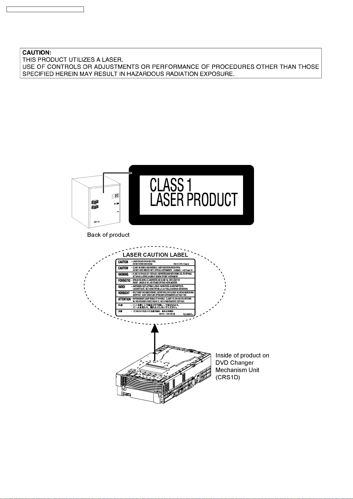
3 Precaution of Laser Diode
CAUTION :
This product utilizes a laser diode with the unit turned on, invisible laser radiation is emitted from the pickup lens.
Wavelength : 662nm (DVD)/785nm (CD)
Maximum output radiation power from pickup : 100µW/VDE
Laser radiation from pickup unit is safety level, but be sure the followings:
1. Do not disassemble the pickup unit, since radiation from exposed laser diode is dangerous.
2. Do not adjust the variable resistor on the pickup unit. It was already adjusted.
3. Do not look at the focus lens using optical instruments.
4. Recommend not to look at pickup lens for a long time.
10
Page 11
SA-VK860GC / SA-VK860GCS / SA-VK860GS
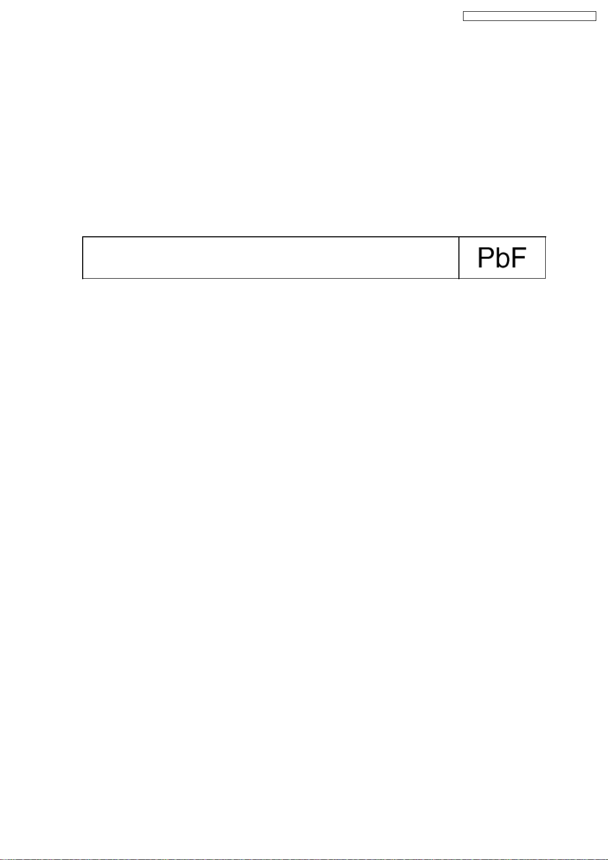
4 About Lead Free Solder (PbF)
4.1. Service caution based on legal restrictions
4.1.1. General description about Lead Free Solder (PbF)
The lead free solder has been used in the mounting process of all electrical components on the printed circuit boards used for this
equipment in considering the globally environmental conservation.
The normal solder is the alloy of tin (Sn) and lead (Pb). On the other hand, the lead free solder is the alloy mainly consists of tin
(Sn), silver (Ag) and Copper (Cu), and the melting point of the lead free solder is higher approx.30 degrees C (86°F) more than that
of the normal s older.
Definition of PCB Lead Free Solder being used
The letter of “PbF” is printed either foil side or components side on the PCB using the lead free solder.
(See right figure)
Service caution for repair work using Lead Free Solder (PbF)
•
• The lead free solder has to be used when repairing the equipment for which the lead free solder is used.
• •
(Definition: The letter of “PbF” is printed on the PCB using the lead free solder.)
•
• To put lead free solder, it should be well molten and mixed with the original lead free solder.
• •
•
• Remove the remaining lead free solder on the PCB cleanly for soldering of the new IC.
• •
•
• Since the melting point of the lead free solder is higher than that of the normal lead solder, it takes the longer time to melt
• •
the lead free solder.
•
• Use the soldering iron (more than 70W) equipped with the temperature control after setting the temperature at 350±30
• •
degrees C (662±86°F).
Recommended Lead Free Solder (Service Parts Route.)
•
• The following 3 types of lead free solder are available through the service parts route.
• •
RFKZ03D01K-----------(0.3mm 100g Reel)
RFKZ06D01K-----------(0.6mm 100g Reel)
RFKZ10D01K-----------(1.0mm 100g Reel)
Note
* Ingredient: tin (Sn), 96.5%, silver (Ag) 3.0%, Copper (Cu) 0.5%, Cobalt (Co) / Germanium (Ge) 0.1 to 0 .3%
11
Page 12
SA-VK860GC / SA-VK860GCS / SA-VK860GS
5 Handling Precautions for Traverse Unit
The laser diode used inside optical pickup could be destroyed due to static electricity as a potential difference is caused by
electrostatic load discharged from clothes or human body. Handling the parts carefully to avoid electrostatic destruction during
repair.
5.1. Handling Optical Pickup in Traverse Unit
1. Do not impact on optical pickup as the unit structurally uses an extremely precise technology.
2. Short-circuit the flexible cable of optical pickup remove from the circuit board using a short-circuit pin or clip in order to prevent
laser diode from electrostatic destruction (Refer to Fig. 5.1 and Fig. 5.2)
3. Do not handle flexible cables forcibly as this may cause snapping. Handle the parts carefully (Refer to Fig. 5.1)
4. A new optical pickup is equipped with an anti-static flexible cable. After replacing and connecting to the flexible board, cut the
anti-static flexible cable. (Refer to Fig. 5.1)
Fig. 5.1
5.2. Replacing Precautions for Optical Pickup Unit
Optical Pickup
The optical pickup by which part supply was carried out attaches the short clip to the flexible board for laser diode electrostatic
discharge damage prevention. Please remove the short clip and be sure to check that the short land is open, before connecting.
(Please remove solder, when the short land short-circuits.)
5.3. Grounding for Preventing Electrostatic Destruction
1. Human body grounding
Use the anti-static wrist strap to discharge the static electricity accumulated in your body. (Refer to Fig. 5.2)
2. Work place grounding
Place a conductive material (conductive sheet) or ironboard where optical pickup is placed. (Refer to Fig. 5.2)
Note :
Keep your clothes away from optical pickup as wrist strap does not release the static electricity charged in clothes.
12
Page 13
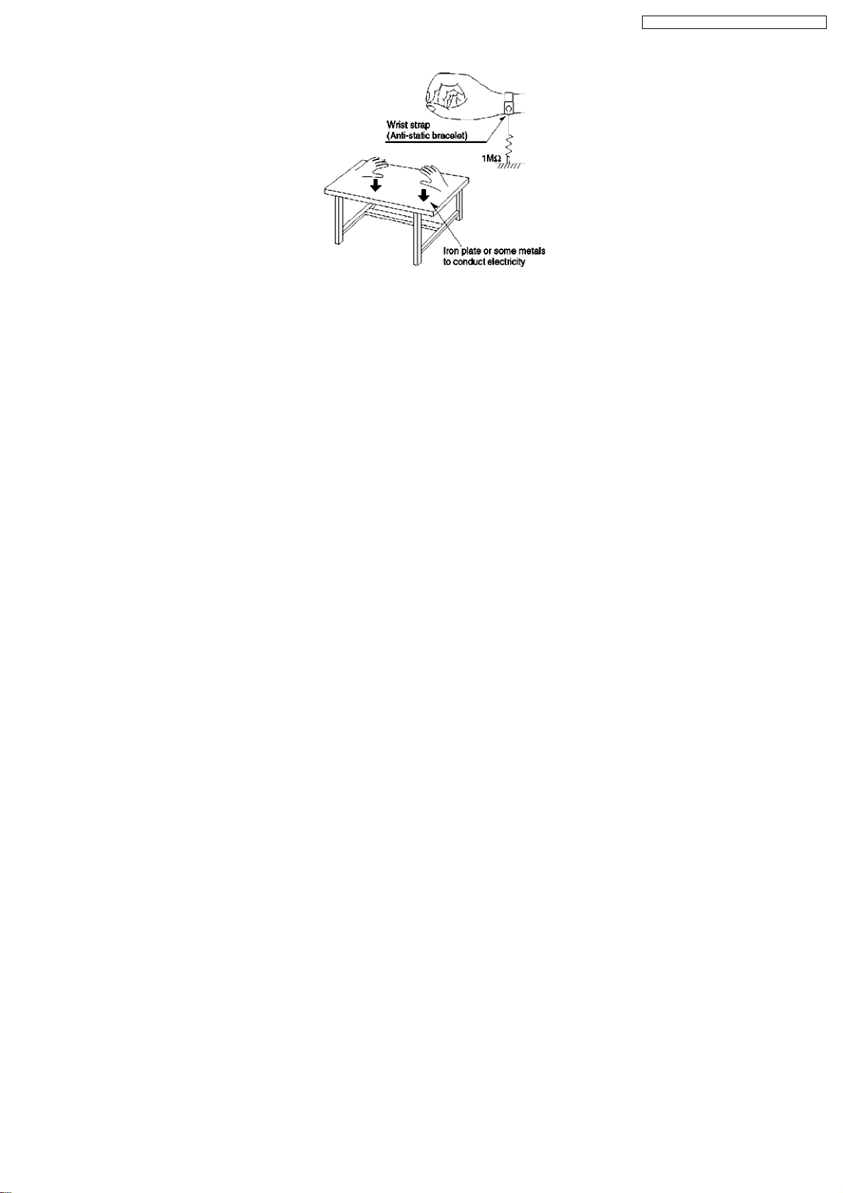
Fig. 5.2
SA-VK860GC / SA-VK860GCS / SA-VK860GS
13
Page 14
SA-VK860GC / SA-VK860GCS / SA-VK860GS
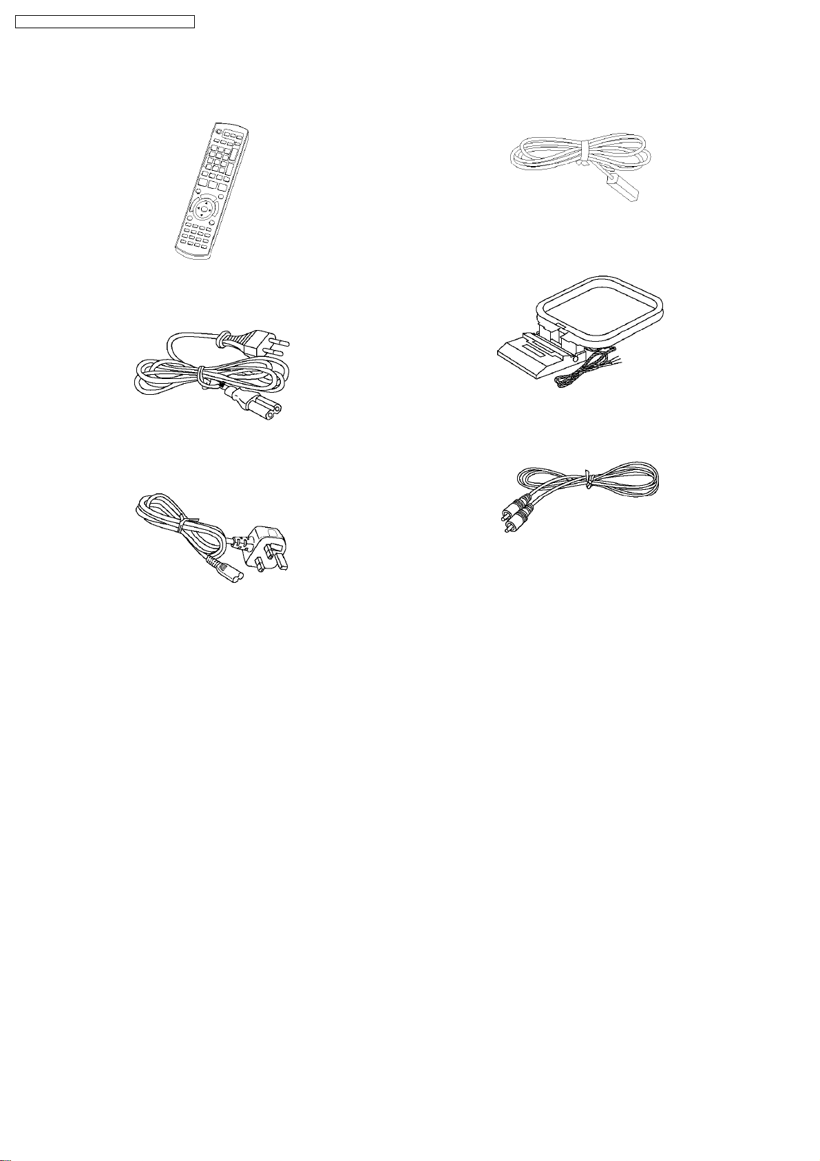
6 Accessories
•
• Note: Refer to “Replacement Parts List” (Section 23) for the part number.
• •
Remote control
FM antenna wire
AM loop antenna
AC cord (For GC/GCS/GS)
AC cord (For GS only)
Video cable
14
Page 15
7 Operation Procedures
7.1. Main Unit Key Buttons Operations
Refer to the numbers in parentheses for page reference. Buttons such as function the same as the controls on the
remote control.
AC supply indicator [AC IN ]
This indicator lights when the unit is
connected to the AC mains supply.
Standby/on switch [ /l]
Press to switch the unit from on
to standby mode or vice versa.
In standby mode, the unit is still
consuming a small amount of
[SURROUND ENHANCER]
[SUPER SURROUND]
[SUPER SOUND EQ]
[SUBWOOFER]
MUSIC PORT jack
Headphone jack
Avoid listening for prolonged
periods of time to prevent hearing
Plug type
Deck 1 [ , OPEN]
[BAND, TUNER]
[DISPLAY
Deck 1 cassette holder
power.
[SOUND EQ]
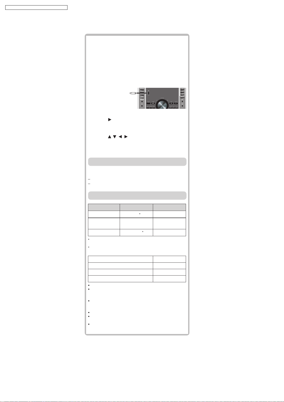
USB port
[ , USB]
Display
damage.
3.5 mm stereo
(not included)
[EXT-IN]
DEMO]
[DECK 1/2]
, RECORD]
[
SA-VK860GC / SA-VK860GCS / SA-VK860GS
Remote control signal
sensor
Disc trays
[
, OPEN /CLOSE]
[
, MULTI CHANGE]
[
, SINGLE CHANGE]
] to [5 ]
[1
(disc direct play)
MIC VOL ]
[ , DVD/CD ]
Microphone ( MIC 1, MIC 2)
jacks
, STOP]
[
Deck 2 [OPEN,
Disc skip/search, tape
fast-forward/ rewind,
tuning, time adjustment
[ , / REW] ,
[ , / FF]
[ , TAPE]
VOLUM E
Deck 2 cassette holder
]
To select the desired display mode
Every time you press the button:
Normal Peak hold Refl ection
Off
Normal
Indicates strength of the sound in each tonal range.
Peak hold
Peak sound value of each sound range (on display for about one second after it occurs).
Refl ection
Indicates the strength of the sound in each tonal range (displayed in the opposite direction of normal
mode).
15
Page 16
SA-VK860GC / SA-VK860GCS / SA-VK860GS
7.2. Remote Control Key Buttons Operations
Buttons labelled such as function in exactly the same way as the buttons on the main unit.
[DIRECT NAVIGATOR, TOP MENU ]
1
Television operations
1
[CLOCK/TIMER]
PLAY/REC]
[
Numeric
[DISC]
3
4
2
6
[SLEEP/A.OFF]
7
[]
[]
5
[DIMMER]
][PLAY MODE CD MODE
[SURROUND ENHANCER ]
[ , , , ], [ ENTER]
[FUNCTIONS]
[MENU, PLAYLIST]
Disc skip, tape fast-forward/rewind, preset
channel selection, time adjustment
[, / REW] , [ , / FF]
[SUBWOOFER]
[SOUND]
[V.MUTE] [ , #]
[ECHO] [AUDIO]
To mute the sound. To dim the display panel.
Press the button to
activate.
Press the button again
or adjust the volume to
cancel.
Muting is also canceled
when you switch the
unit to standby.
Every time you press the button.
Setting Effect
1 Display and ambient light
2 Display dims and ambient
3Original
dims
light is turned off
brightness
The display is dimmed, but brightens
when you perform some operations.
[RETURN,
[ , , SLOW/ SE ARCH ]
[FL DISPLAY]
[REPEAT]
[C.FOCUS]
[MUTING, CANCEL]
[CH SELECT
SETUP]
TEST]
This auto off function allows you to turn off the
unit in disc or tape mode only after left unused
for 10 minutes.
Every time you press the button:
SLEEP 30 SLEEP 60 SLEEP 90 SLEEP 120
SLEEP OFF
AUTO OFF
The setting is maintained even if the unit is
turned off.
If you select tuner or music port as the source,
"AUTO OFF" turns off. It comes on again when
you select disc or tape.
16
Page 17
7.3. Portable Audio Equipment Connection & Operation
Connecting to a portable audio equipment
Playing or recording from a portable
audio equipment
Before connection
Disconnect the AC power supply cord.
Turn off all equipment and read the appropriate operating
instructions.
The equipment connections described are examples
only.
Peripheral equipment and optional cables are sold
separately unless otherwise indicated.
Connecting to a portable audio equipment
This feature enables you to enjoy music from a portable
audio equipment.
audio equipment
Switch off the equalizer function (if there is any) of
the portable audio equipment before you plug into the
MUSIC PORT jack. Otherwise, sound from the speaker
may be distorted.
Plug the audio cord into the MUSIC PORT jack and
1
press [EXT-IN] to select "MUSIC PORT".
MUSIC PORT AUX
For listening : Proceed to step 3.
2
For recording : Press [ , RECORD] on the main
Start playback from the portable audio
3
equipment. (See the portable audio equipment’s
instruction manual.
unit to start recording.
5SUBWOOFER
Playing or recording from a portable
SA-VK860GC / SA-VK860GCS / SA-VK860GS
17
Page 18
SA-VK860GC / SA-VK860GCS / SA-VK860GS
7.4. USB Connection & Operation
The USB connectivity enables you to connect and play
tracks or les from USB mass storage class devices.
Typically, USB memory devices. (Bulk only transfer)
Preparation
Before connecting any USB mass storage device to
the unit, ensure that the data stored therein has been
backed up.
It is not recommended to use a USB extension cable.
The USB device is not recognised by this unit.
Connect the USB mass storage device (not
1
included).
USB enabled device
(not included)
It is not recommended to
use a USB extension cable.
The device connected via
the cable will not be recognised by this unit.
Press [ , USB] to begin playback.
2
Press [TOP MENU] or [MENU] to display the USB
3
menu.
Press [ , , , ] and then [ENTER] to select
4
the desired item.
For other operating functions, they are similar as those
described in "DISC OPERATIONS".
Compatible Devices
Devices which are defi ned as USB mass storage
class:
USB devices that support bulk only transfer.
USB devices that support USB 2.0 full speed.
Supported Formats
File name File extension
Still pictures JPG
1
Music MP3
WMA
2
Video MPEG4
1
It may not be possible to play all the fi les due to the condition
on how they were created.
2
For Panasonic D-Snap/DIGA
.jpg .jpeg
.mp3
.wma
.asf
Note:
Maximum number of folders 400
Maximum number of fi les 4000
Maximum length of folder name 44
Maximum length of fi le name 44
CBI (Control /Bulk/Interrupt) is not supported.
Digital Cameras that use PTP protocol or which require
additional program installation when connected to a PC are
not supported.
A device using NTFS fi le system is not supported.
[Only FAT 12/16/32 (File Allocation Table 12/16/ 32) fi le
system is supported].
Depending on the sector size, some fi les may not work.
It will not operate with Janus enabled MTP (Media Transfer
Protocol) devices.
Only one memor y card will be selected when connecting a
multi-port USB card reader. Typically the fi rst memory card
inserted.
18
Page 19

7.5. About DivX VOD Content
SA-VK860GC / SA-VK860GCS / SA-VK860GS
DivX Video-on-Demand (VOD) content is encr ypted for
copyright protection. In order to play DivX VOD content on
this unit, you first need to register the unit.
Follow the online instructions for purchasing DivX VOD
content to enter the unit’s registration code and register the
unit. For more information about DivX VOD, visit
www.divx.com/vod.
Display the unit’s registration code
("DivX Registration" in "Others" tab)
put
eS
csiD
oediV
oiduA
ruoY
yalpsiD
srehtO
P
We recommend that you make a note of this code for
future reference.
After playing DivX VOD content for the first time, another
registration code is then displayed in "DivX Registration".
Do not use this registration code to purchase DivX VOD
content. If you use this code to purchase DivX VOD
content, and then play the content on this unit, you will
no longer be able to play any content that you purchased
using the previous code.
If you purchase DivX VOD content using a registration
code different from this unit’s code, you will not be able
to play this content. ("Authorization Error" is displayed.)
noitartsigeR XviD
dnameD-no-oediV XviD
XXXXXXXX
edoc noitartsiger
: si
RETNE
nitnoc otsser
eu
dov/moc.xvid.www tisiv erom nrael oT
8 alphanumeric
characters
Regarding DivX content that can only be played a
set number of times
Some DivX VOD content can only be played a set number
of times. When you play this content, the remaining number
of plays is displayed. You cannot play this content when the
number of remaining plays is zero.
("Rented Movie Expired" or "Rental Expired" is displayed.)
When playing this content
The number of remaining plays is reduced by one if
you press
you press
you press , ] (skip) or [ , ] (search)
arrive at another content or the start of the content
being played.
The "Resume" function and "Marker" functions will not
work.
[ ]
or press and hold [ SETUP].
[ ]
. [Press [ ] (pause) to pause play.]
[
etc. and
19
Page 20
SA-VK860GC / SA-VK860GCS / SA-VK860GS
7.6. Disc Information
7.6.1. Disc Playability (Media)
Commercial discs
Disc Logo
Indicated in
these
ctions by
instru
Remarks
DVD-Video
Video CD
CD
Recorded discs
Disc Logo
DVD-RAM
DVD-R/ RW
DVD-R DL
+R/+RW
+R DL
CD-R/RW
1
( : Playable, : Not playable)
Recorded on a DVD
video record er, etc.
3
High quality movie and music discs.
Music discs with video.
Including SVCD (Conforming to IEC62107).
Music discs.
Recorded on a personal computer, etc.
8
()
()
42
5
5
9
Finalizing
Not
necessary
N
ecessar
N
ecessar
N
ecessar
N
ecessar
N
ecessar
6
y
y
y
y
7
y
It may not be possible to play all the above-mentioned discs in some cases due to the type of disc, the condition of the
recording, the recording method, or how the files were created. [Refer to Section 7.6.2. File Extension Type Support (WMA/MP3/
1
This unit c an play CD-R/ RW recorded with CD-DA or Video CD format.
This unit also plays HighMAT discs.
2
Discs recorded on DVD video recorder s or DVD video cameras, etc. using Version 1.1 of the Video Recording Format (a unified video
recording standard).
3
Discs recorded on DVD video recorder s or DVD video cameras using Version 1.2 of t he Video Recording Format (a unifi ed video
recording standard).
4
Discs recorded on DVD video recorder s or DVD video cameras using DVD-Video Format.
5
Recorded using a format different from DVD-Video Format, therefore, some functions cannot be used.
6
A process that allows play on compatible equipment. To play a disc that is displayed as "Necessary" on this unit, the disc must first be
finalize d on the device it was recorded on.
7
Closing the session will also work.
8
MPEG4 dat a recorded with the Panasonic SD multi cameras or DVD video recorders [conformin g to SD VIDEO specif ications (ASF
standard)/MPEG4 (Simple Pro f ile) video system/G.726 audio system].
9
Functions added with DivX Ultra are not supported.
JPEG/MPEG4/DivX)
Note about using a DualDisc
The digital audio content side of a DualDisc does not meet the
technical speci
(CD-DA) format so playback may not be possible.
Discs that cannot be played
ations of the Compact Disc Digital Aud io
fic
DVD-RW version 1.0, DVD-Audio, DVD-ROM, CD-ROM,
CDV, CD-G, SACD, Photo CD, DVD-RAM that cannot be
removed from their cartridge, 2.6 GB and 5.2 GB DVDRAM, and "Chaoji VCD" available on the market including
CVD, DVCD and SVCD that do not conform to IEC62107.
Video systems
This unit can play PAL and NTSC, but your television
must match the system used on the disc.
PAL discs cannot be correctly viewed on an NTSC
television.
This unit can convert NTSC signals to PAL 60 for
viewing on a PAL television ( Refer to "NTSC Disc
Output" in "Video" tab of the OI book).
20
Page 21
7.6.2. File Extension Type Support (WMA/MP3/JPEG/MPEG4/DivX)
SA-VK860GC / SA-VK860GCS / SA-VK860GS
When there are more than eight groups, the eighth group
onwards will be displayed on one vertical line in the
menu screen.
There may be differences in the display order on the
menu screen and computer screen.
This unit cannot play files recorded using packet write.
DVD-RAM
Discs must conform to UDF 2.0.
DVD-R/RW
Discs must conform to UDF bridge (UDF 1.02/ISO9660).
This unit does not suppor t multi-session. Only the default
session is played.
CD-R/RW
Discs must conform to ISO9660 level 1 or 2 (except for
extended formats).
This unit suppor ts multi-session but if there are many
sessions it takes more time for play to start. Keep the
number of sessions to a minimum to avoid this.
Naming folders and files
Files are treated as contents and
folders are treated as groups on this
unit.
At the time of recording, prefi x folder
and file names. This should be with
numbers that have an equal number
of digits, and should be done in the
order you want to play them (this may
not work at times). Files must have the
extension ( see below).
(Extension: ".WMA" or ".wma")
Compatible compression rate:
between 48 kbps and 320 kbps.
You cannot play WMA files that are copy-protected.
This unit does not suppor t Multiple Bit Rate (MBR).
(Extension: ".MP3" or ".mp3")
Compatible compression rate: between 32 kbps and
320 kbps.
This unit does not suppor t ID3 tags.
Compatible sampling rates:
DVD-RAM, DVD-R/RW: 11.02, 12, 22.05, 24, 44.1 and
4848 kHz
CD-R/RW: 8, 11.02, 12, 16, 22.05, 24, 32, 44.1 and
kHz
Example:
MP3
root
(Extension: ".JPG", ".jpg", ".JPEG" or ".jpeg")
JPEG fi les taken on a digital camera that conform to DCF
Standard (Design rule for Camera File system) Version
1.0 are displayed. Files that have been altered, edited or
saved with computer picture editing software may not be
displayed.
This unit cannot display moving pictures, MOTION JPEG
and other such formats, and still pictures other than
JPEG (Example: TIFF), or play pictures with attached
audio.
(Extension: ".ASF" or ".asf")
You can play MPEG4 data [conforming to SD VIDEO
specifications (ASF standard)/MPEG4 (Simple Profile)
video system/G.726 audio system] recorded with
Panasonic SD multi cameras or DVD video recorders
with this unit.
The recording date may differ from that of the actual
date.
(Extens ion: ".DIVX", ".d ivx", ".AVI" or ".avi")
You can play all versions of DivX
DivX 6) [DivX video system/MP3, Dolby Digital or MPEG
audio system] with standard playback of DivX
files. Functions added with DivX Ultra are not supported.
DivX files greater than 2 GB or have no index may not be
played properly on this unit.
This unit suppor ts all resolutions up to maximum of 720 x
480 (NTSC)/720 x 576 (PAL).
You can select up to eight types of audio and subtitles on
this unit.
video (including
media
21
Page 22

SA-VK860GC / SA-VK860GCS / SA-VK860GS
8 DVD/CD Changer Mechanism Unit
8.1. CRS1D Mechanism Overview
22
Page 23
SA-VK860GC / SA-VK860GCS / SA-VK860GS
8.1.1. General Feature
•
• This is a five disc changer mechanism for CD/DVD. The outline figure is shown below.
• •
•
• The mechanism has "CHANGE WHILE PLAY" function. It open other trays for disc exchanging while one tray is at PLAY
• •
position performing recording or reproducing.
•
• The mechanism can quickly change all trays with "CHANGE ALL" function. All trays can be move to OPEN position with one
• •
operation.
•
• There is no sensor to indicate presence of disc on any tray.
• •
8.1.2. Hardware Composition
•
• Below is the hardware components of the mechanism
• •
Name Function
Open Switch (OPEN-SW) The switch is used to detect normal tray opening
The switch is used for detect tray being manually push/trigger when full open
Home Switch (HOME-SW) Is used to detect cam gear home position
Close Sensor (CLOSE-SENSOR) Used for normal single tray closing
Used to detect cam gear rotate to Play Driving position
Play Switch (PLAY-SW) Detect TRV clamping complete position
Stocking Switch (STOCK-SW) Detect tray completely transfer for play position to stocking position
UD Sensor (UD-SENSOR) Detect TRV vertical movement position
Top Switch (TOP-SW) Detect a default position of TRV vertical movement position
Driver IC To drive Motor
Motor Main driving source for changer
Plunger Switching the driving source from motor to:
1. Tray open/close
2. Drive tray to play/stock position and TRV vertical movement
8.1.3. Mechanism Operation
•
• This mechanism has the following state:
• •
1. Driving of a tray to open/close
2. Up/down operation of a traverse performs a state changes of tray.
By using the plunger to lift/release of a switching gear, and the cam gear to lift/release the function gear the motor can be link
to several gear trains to perform various operations.
•
• The functions that can be perform in this mechanism are described as below:
• •
Condition Explanation
Open current playing tray The state to change current playing disc. All tray will be open at once and current tray at PLAY position
Open All The state where all trays being driven to OPEN position. The disc can be taken in or out from tray to tray
Stock The state where the trays are stored in STOCK position
Play The state where one of the tray 5 trays is being driven to PLAY position and clamped by traverse unit
Play & Open Tray-* The state where one of the tray is in playing position performing recording or reproducing, other trays can
will be expose.
by close tray one by one from top to bottom.
be used (OPEN position) for disc exchanging without stopping the recording or reproducing process.
23
Page 24

SA-VK860GC / SA-VK860GCS / SA-VK860GS
Condition Explanation
Change The state when one of the opened tray being driven from OPEN position to STOCK position and other
Close All The state where all open trays will being driven from OPEN position to STOCK position, one by one from
Note: * represent tray number (from 1 ~ 5)
opened trays remain still at OPEN position.
top to bottom
8.1.4. DVD/CD Changer Mechanism Unit (CRS1D) Information
Note:
This service manual does not contain the following information for the mentioned DVD/CD changer mechanism unit:
•
• Schematic Diagram, Block Diagram and P.C.B. layout of CD/DVD Loading P.C.B.
• •
•
• Part List for individual parts of the mechanism.
• •
•
• Exploded View and Parts List for individual parts of the DVD/CD changer mechanism unit.
• •
24
Page 25
SA-VK860GC / SA-VK860GCS / SA-VK860GS
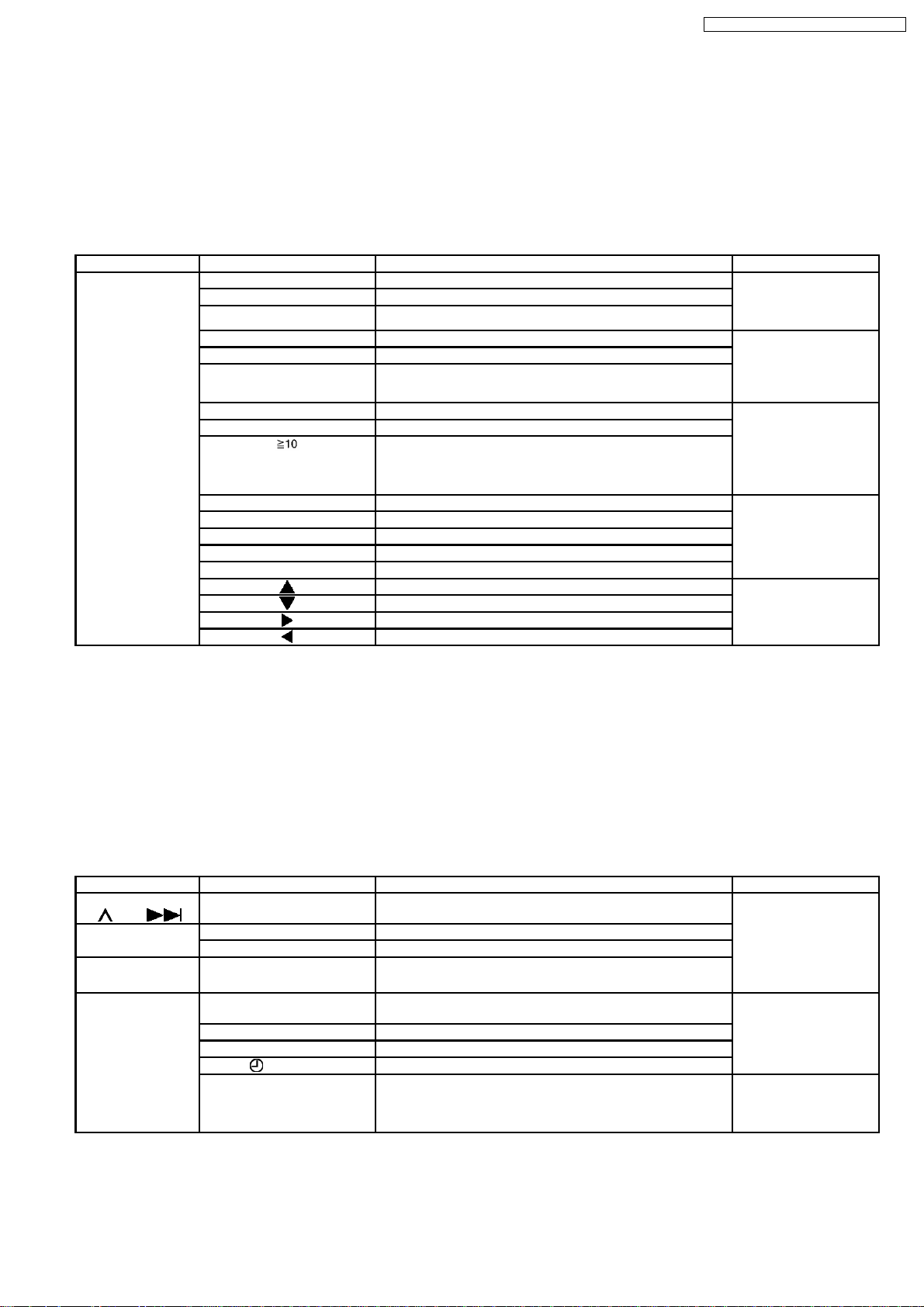
9 Self Diagnosis and Special Mode Setting
This unit is equipped with functions for checking and inspecting.
9.1. Service Mode Summary Table
9.1.1. Service Mode Summary Table (For DVD)
The service modes can be activated by pressing various button combination on the main unit and remote control unit.
Below is the summary for the various modes for checking:
Main buttons Remote control unit buttons Application Note
[STOP] [0] Error code display. (Refer to the section
[5] Jitter checking.
[PAUSE] Initial setting of laser drive current.
[FUNCTIONS] DVD laser drive current check. (Refer to the section
[1] ADSC internal RAM data check.
[3] CD laser drive current check.
“9.2.1. Service Mode
Table 1” for more
information.)
“9.2.2. Service Mode
Table 2” for more
information.)
[6] Region display and mode. (Refer to the section
[7] Micro-processor firmware version check.
[ ] Initialization of the player (factory setting is restored).
Used after replacement of Micro-processor (DV5 LSI) IC, FLASH
ROM IC (IC8651), EEPROM IC (IC8611) and DVD Module
P.C.B.
[8] DVD Module P.C.B. firmware version check. (Refer to the section
[MENU] Communication error display.
[TOP MENU] ECC error check.
[DISC] CPPM/CRM keys check.
[ENTER] DVD Module P.C.B. reset.
[ ] Timer 1 check. (Refer to the section
[ ] Timer 1 reset.
[ ] Timer 2 check.
[ ] Timer 2 reset.
“9.2.3. Service Mode
Table 3“ for more
information.)
“9.2.4. Service Mode
Table 4“ for more
information.)
“9.2.5. Service Mode
Table 5“ for more
information.)
Note:
An error code will be canceled if a power supply is turned OFF.
*1: CPPM is the copy guard function beforehand written in the disk for protection of copyrights.
*2: CEC is the consumer electronic control used for high-level user control of HDMI-connected devices.
*3: HDCP is the specification developed to control digital audio & video contents transmission for DVI or HDMI connections.
9.1.2. Service Mode Summary Table (For Inspection)
Main buttons Remote control unit buttons Application Note
[STOP] +
/FF/ ]
[
In Self-diagnostic
Mode
[STOP] [4] + [7] Entering doctor mode.
In Doctor Mode [STOP] button on the main
[SINGLE CHANGE] Servicing the traverse unit.
[ PLAY/REC] FL display test.
- Entering self-diagnostic mode. (Refer to the section
[1] DVD/CD Changer Mechanism Reliability Test.
Firmware version check. (Refer to the section
unit + [4] + [7]
[4] Cold start.
[0] Tape eject test.
[DISC] DVD/CD changer operation check. (Refer to the section
“9.3.1. Service Mode
Table 1” for more
information.)
“9.3.2. Service Mode
Table 2“ for more
information.)
“9.3.3. Service Mode
Table 3“ for more
information.)
25
Page 26
SA-VK860GC / SA-VK860GCS / SA-VK860GS
9.2. Service Mode Table (For DVD)
By pressing various button combinations on the player and remote control unit can activate the various service modes for checking.
Special Note:
Due to the limitations of the no. characters that can be shown on FL Display, the “FL Display” button on the remote control unit
is used to show the following page. (Display 1 / Display 2).
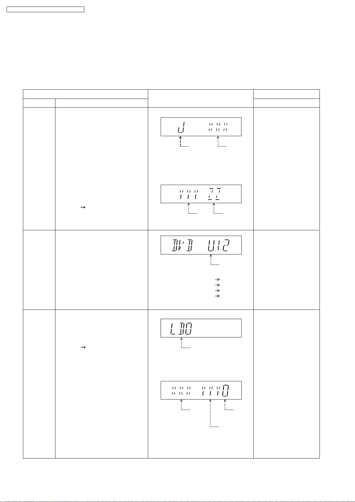
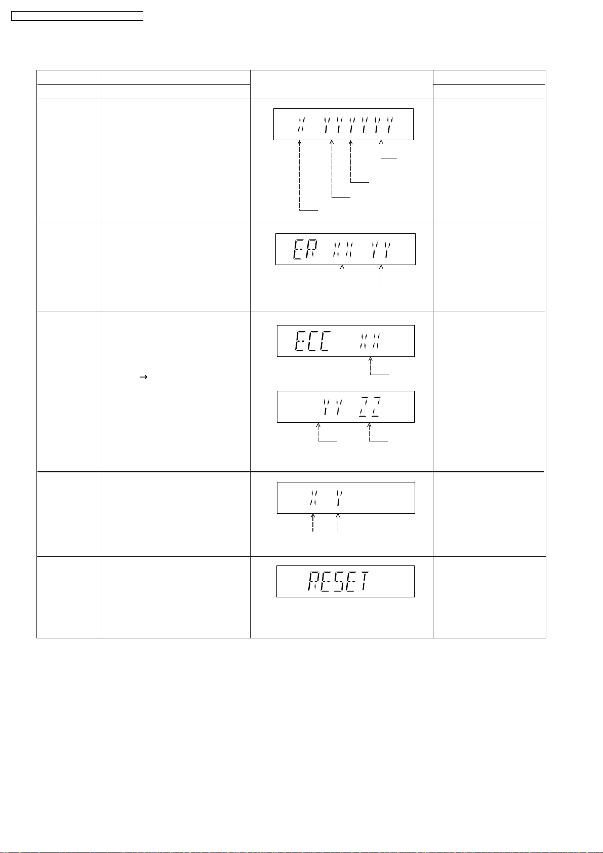
9.2.1. Service Mode Table 1
Mode Name
Jitter check
Error code
display
Item
Description
Jitter check.
Jitter rate is measured and displayed.
Measurement is repeatedly done in
the cycle of one second. Read error
counter starts from zero upon mode
setting.
When target block data failed to be
read out, the counter advances by one
increment. When the failure is caused
by minor error, it may be corrected
when retried to enable successful
reading.
In this case, the counter advances by
one. When the error persists even
after retry, the counter may jump by
two or more.
FL Display sequence:
Display 1 2.
Error code check
The latest error code stored in the
EEPROM IC is displayed.
Note: Refer to "Section 9.4 DVD Self
Diagnostic Function-Error Code" for
more detailed information on the error
codes.
FL Display
(Display 1)
Jitter Check
Mode
Jitter rate is shown in decimal notation to
one place of decimal.
Focus drive value is shown in hexadecimal
notation.
(Display 2)
Lead
Error
Counter
Error code (play_err) is expressed in the
following convention.
Error code = 0 x DAXX is expressed: DVDnn U12
Error code = 0 x DBXX is expressed: DVDnn H12
Error code = 0 x DXXX is expressed: DVDnn F123
Error code = 0 x 0000 is expressed: DVDnn F--* "xx" denotes the error code
Jitter Rate
Focus Drive
Value
U / H / F
Key Operation
Front Key
In STOP (no disc) mode,
press [STOP] button on the
main unit, and [5] button on
the remote control unit.
Press [STOP] button to
exit.
Press [FL Display] on
remote control unit for next
page (FL Display).
In STOP (no disc) mode,
press [STOP] button on the
main unit, and [0] button on
the remote control unit. * With
pointing of cursor up and
down on display.
Cancelled automatically
5 seconds later.
To exit, press [POWER]
button on main unit or
remote control.
Initial setting
of laser drive
current
Initial setting of laser drive current.
Initial current value for the DVD laser
and CD laser is separately saved in
the EEPROM IC.
FL Display sequence:
Display 1 2.
(Display 1)
Laser Current
Measurement
The value denotes the current in decimal
notation.
(Display 2)
The above example shows the initial
current is XXXmA and YYYmA for CD
laser and DVD laser respectively when
the laser is switched on.
Mode
CD
Laser
Identify
as LDO
mode
DVD Laser
26
In STOP (no disc) mode,
press [STOP] button on the
main unit, and [PAUSE]
button on the remote
control unit.
Cancelled automatically
5 seconds later.
Press [FL Display] on
remote control unit for next
page (FL Display) on values
of laser drive current.
Page 27
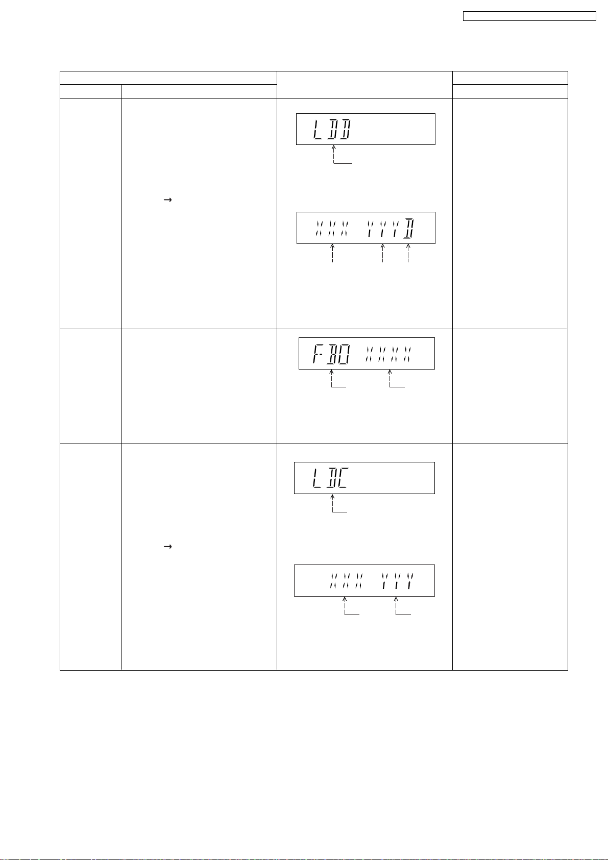
9.2.2. Service Mode Table 2
SA-VK860GC / SA-VK860GCS / SA-VK860GS
DVD laser
drive current
measurement
ADSC internal
RAM data
check
Item
DescriptionMode Name
DVD laser drive current measurement.
DVD laser drive current is measured
and the result is displayed together
with the initial value stored in the
EEPROM IC.
After the measurement, DVD laser
emission is kept on. It is turned off
when POWER key is switched off.
FL Display sequence:
Display 1 2.
ADSC internal RAM data check.
ADSC internal RAM data is read out
and displayed.
FL Display
(Display 1)
DVD laser current
measurement mode
The value denotes the current in decimal
notation.
(Display 2)
DVD
DVD
Laser
Initial Value
The above example shows the initial
current is XXXmA and the measured
value is YYYmA.
Address
The value is shown in hexadecimal
notation. The above example shows the
data in ADSC address FBOh is XXXXh.
Laser
Value
Identify as
LDD mode
RAM Data
for Specified
Address
Key Operation
Front Key
In STOP (no disc) mode,
press [STOP] button on the
main unit, and
[FUNCTIONS] button on
the remote control unit.
Cancelled automatically
5 seconds later.
Press [FL Display] on
remote control unit for next
page (FL Display) on values
of dvd drive current.
In STOP (no disc) mode,
press [STOP] button on the
main unit, and [1] or [2]
button on the remote control
unit.
To exit, press [STOP]
button.
CD laser drive
current
measurement
CD laser drive current measurement.
CD laser drive current is measured
and the result is displayed together
with the initial value stored in the
EEPROM IC.
After the measurement, CD laser
emission is kept on. It is turned off
when POWER key is switched off.
FL Display sequence:
Display 1 2.
(Display 1)
CD Laser Current
Measurement Mode
The value denotes the current in decimal
notation.
(Display 2)
CD
Laser Initial
Value
The above example shows the initial current
is XXXmA and the measured value is
YYYmA.
CD Laser
Value
In STOP (no disc) mode,
press [STOP] button on
the main unit, and [3]
button on the remote
control unit.
Cancelled automatically
5 seconds later.
Press [FL Display] on
remote control unit for next
page. (FL Display)
27
Page 28
SA-VK860GC / SA-VK860GCS / SA-VK860GS
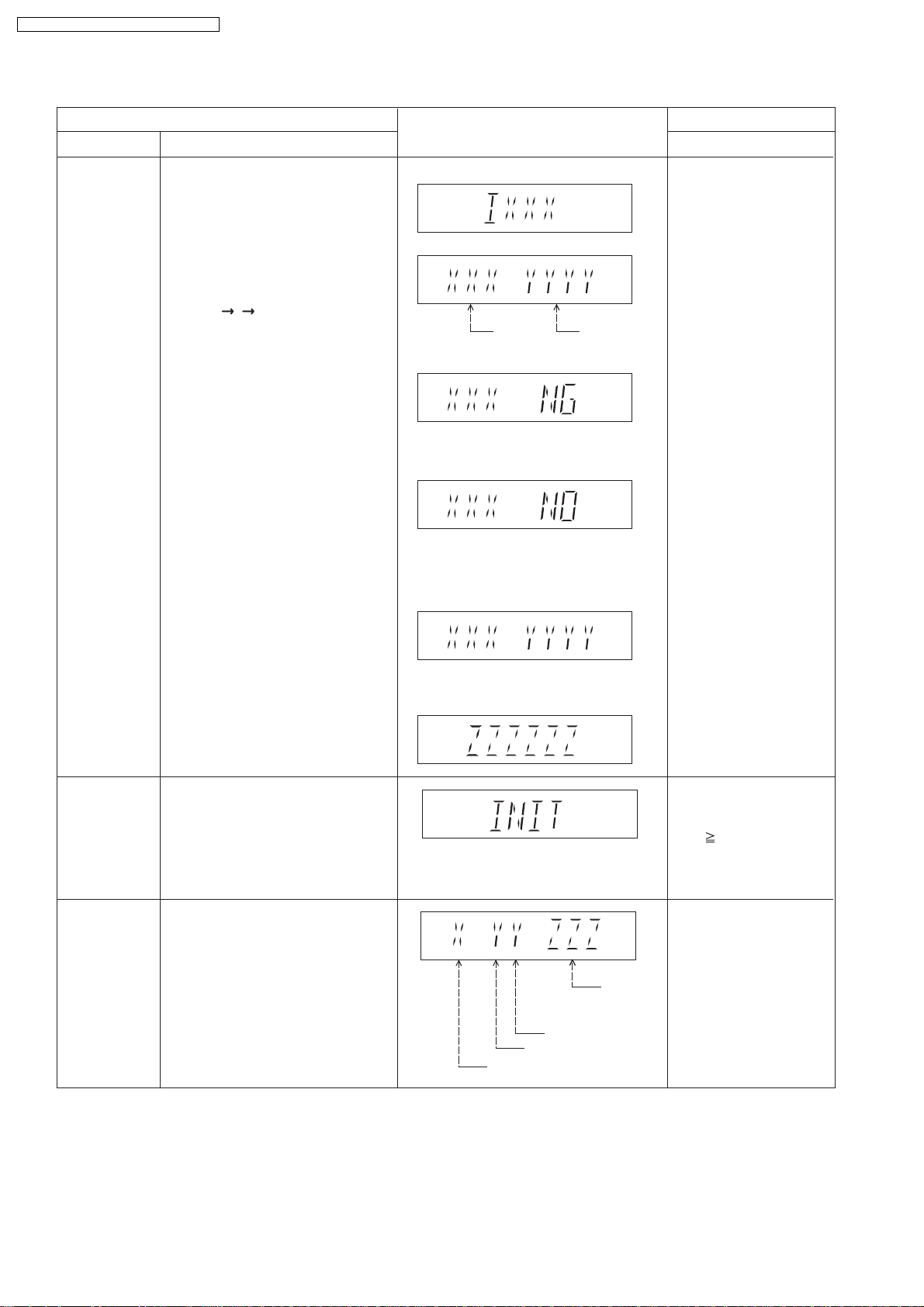
9.2.3. Service Mode Table 3
Micro-processor
firmware version
display &
EEPROM
checksum
display.
Item
DescriptionMode Name
Micro-processor firmware version
display & EEPROM checksum display.
EEPROM checksum is only available
due to existence of EEPROM IC.
Note: Condition 1/2/3 shows the state
of EEPROM IC. It is indicated in
Display 2.
FL Display sequence:
Display 1 2 3.
FL Display
(Display 1)
(Display 2)
Opecon
Version
(Condition1)
If the version of the EEPROM does not match,
[NG] is displayed.
(Condition 2)
(a) If there is NO EEPROM header string
OR
(b) If there is no EEPROM (no data is received
by Micro-processor), [NO] is displayed.
(Condition 3)
EEPROM
Checksum
(If applicable,
refer below.)
Key Operation
Front Key
In STOP (no disc)
mode, press [STOP]
button on the main unit,
and [7] button on the
remote control unit.
Cancelled automatically
5 seconds later.
Initialization
mode
Region display
Initialization.
User settings are cancelled and player
is initialized to factory setting.
It is necessary when after replacement
of Micro-processor (DV5 LSI) IC,
FLASH ROM IC (IC8651), EEPROM
IC (IC8611) & DVD Module P.C.B.
Region code display, TV broadcasting
system & the model no. information.
Note: Refer to Fig. 9.1 for "Video
Design Information".
If the EEPROM version matches, checksum
[YYYY] is displayed.
(Display 3)
Model
No.
Information
N: NTSC / 6: PAL60
N: no PAL / P: PAL
Region No.: 0-8
Press [FL Display] button on
remote control unit for next
page. (FL Display)
In STOP (no disc)
mode, press [STOP]
button on the main unit,
and [ 10] button on the
remote control unit.
Cancelled automatically
5 seconds later.
In STOP (no disc)
mode, press [STOP]
button on the main unit,
and [6] button on the
remote control unit.
Cancelled automatically
5 seconds later.
28
Page 29
TV Broadcasting
Signal System Region Display
Code
System
(Default) (Default)
English, Spanish, Canadian
French
(S) Japan 2 NTSC NTSC (*A) 2PN Japanese, English
English, French, German,
Spanish, Polish, Russian,
Czech, Hungarian
English, French, German,
Italian, Spanish, Polish,
Swedish, Dutch
English, French, German,
Spanish, Polish, Russian,
Czech, Hungarian
GCS, GD, South East Asia, PAL English, Traditional Chinese
GT, GCT Korea, Taiwan NTSC
New Zealand,
English, French, German,
Australia
Italian, Spanish, Polish,
Swedish, Dutch
Central/South/
NTSC (*D) 4PN
English, Spanish, French,
Latin America Brazilian Portuguese
English, French, German,
Spanish, Polish, Russian,
Czech, Hungarian
GK China 6 PAL NTSC (*B) 6PN English, Simplified Chinese
OSD Menu Language
SA-VK860GC / SA-VK860GCS / SA-VK860GS
Model Series Country Region
Region
P, PC, PX USA, Canada, PX NTSC (*A)
E Europe 2 PAL PAL (*C) 2P6
EB, EG
GC, GS
Europe
Middle East
3 NTSC (*B)
4GN
PL, GCP, LB
NTSC4
Product
1PNNTSC1
2P6PAL (*C)PAL2
2P6PAL (*C)PAL2
3PN
4P6PAL (*C)PAL
EE CIS
NTSC (*A) NTSC (*B)
Source Output Source Output
Screen Saver NTSC Screen Saver NTSC
NTSC disc NTSC
PAL disc
PAL (*C) NTSC (*D)
Screen Saver PAL Screen Saver NTSC
NTSC disc
Source Output Source Output
PAL disc PAL
PAL (DVD-V) PAL60
NTSC (DVD-A/VCD) PAL disc PAL60
PAL60 (default) NTSC disc NTSC
NTSC PAL disc NTSC
NTSC disc
5P6PAL (*C)SECAM5
NTSC (default)
Explanation of Display
Individual Model Code
N: If NTSC disc is played, NTSC output.
6: If NTSC disc is played, PAL60 output.
can play PAL disc
Region code
Fig. 9.1
29
Page 30
SA-VK860GC / SA-VK860GCS / SA-VK860GS
9.2.4. Service Mode Table 4
Mode Name
DVD Module
P.C.B. firmware
version display
Communication
error display
ECC Error
Check
Item
Description
DVD Module P.C.B. firmware version
is displayed on the FL Display.
The firmware version can be updated
using recovery disc.
Note: It is necessary to check for
firmware version before carrying out
the version up using the disc.
Displays frequency of communication
errors between system control IC and
mechanism control IC in the DVD
Module P.C.B.
ECC refers to Error Correction Code. It
describes the error correction code
that was carried out for the decoding
of audio & video.
FL Display sequence:
Display 1 2.
(Display 1)
(Display 2)
FL Display
System controller
generation
Region No.: 0-8
No. of
communication
error
System
controller
version
Destination
No. of
communication
ECC Lead
Error
Key Operation
Front Key
In STOP (no disc)
mode, press [STOP]
button on the main unit,
and [8] button on the
remote control unit.
Cancelled automatically
5 seconds later.
In STOP (no disc)
mode, press [STOP]
button on the main unit,
and [MENU] button on the
remote control unit.
Cancelled automatically
5 seconds later.
In STOP (no disc)
mode, press [STOP]
button on the main unit,
and [TOP MENU] button
on the remote control unit.
Press [STOP] button to
exit.
Press [FL Display] on
remote control unit for next
page (FL Display).
CPPM/CRM
Keys Check
DVD Module
P.C.B. Reset
CPPM/CRM refers to the Content
Protection for Recordable Media and
Pre-Recorded Media. It displays the
existence of the keys as "1" or "0".
OK: Existing of keys.
NG: Non existing of keys.
To reset DVD Module P.C.B.
This process is used when the DVD
Module P.C.B. or FLASH ROM
IC is replaced with a new one.
0: NG
1: OK
Video
Decode
Error
0: NG
1: OK
Audio Lead
Error
In STOP (no disc)
mode, press [STOP]
button on the main unit,
and [DISC] button on the
remote control unit.
Cancelled automatically
5 seconds later.
While in initialization
mode, press & hold
[STOP] button on the main
unit, follow by [ENTER]
button on the remote
control unit.
Cancelled automatically
5 seconds later.
30
Page 31

9.2.5. Service Mode Table 5
SA-VK860GC / SA-VK860GCS / SA-VK860GS
Timer 1 check
Timer 1 reset
Item
DescriptionMode Name
Timer 1 check
Laser operation timer is measured
separately for DVD laser and CD laser.
FL Display sequence:
Display 1 2.
Timer 1 reset
Laser operation timer of both DVD
laser and CD laser is reset all at once.
FL Display
(Display 1)
DVD laser usage time
Shown to the above is DVD laser usage
time, and to the below is CD laser usage
time.
Time is shown in 4 digits of decimal notation
in a unit of 10 hours.
"0000" will follow "9999". (DVD laser)
(Display 2)
CD laser usage time
Time is shown in 4 digits of decimal notation
in a unit of 10 hours.
"0000" will follow "9999". (CD laser)
Time is shown in 4 digits of decimal notation
in a unit of 10 hours.
It will clear to "0000" upon reset.
Key Operation
Front Key
In STOP (no disc)
mode, press [STOP]
button on the main unit,
and [ ] button on the
remote control unit.
Cancelled automatically
5 seconds later.
Press [FL Display] button for
next page of FL Display.
While displaying Timer 1
data, press [STOP] button
on the main unit, and [ ]
button on the remote
control unit.
Cancelled automatically
5 seconds later
Timer 2 check
Timer 2 reset
Timer 2 check
Spindle motor operation timer
Timer 2 reset
Spindle motor operation timer
Time is shown in 5 digits of decimal notation in
a unit of 1 hour.
"00000" will follow "99999".
Time is shown in 5 digits of decimal notation in
a unit of 1 hour.
It will be cleared to "00000" upon activating
this.
In STOP (no disc)
mode, press [STOP]
button on the main unit,
and [ ] button on the
remote control unit.
Cancelled automatically
5 seconds later.
While displaying Timer 2
data, press [STOP] button
on the main unit, and [ ]
button on the remote
control unit.
Cancelled automatically
5 seconds later.
31
Page 32

Note: Press "FL DISPLAY" button on remote
control unit for next page display.
SA-VK860GC / SA-VK860GCS / SA-VK860GS
9.2.6. Optical Pickup Unit Breakdown Diagnosis
The unit is equipped with the optical pickup self-diagnosis function and tilt adjustment check function. Follow the procedure
described below during repair in order to perform self-diagnosis and tilt adjustment effectively. Especially when "NO DISC" is
displayed, be sure to apply the self-diagnosis function before replacing with an optical pickup. Replacement of optical pickup
generally requires when the present value of laser drive exceeds 23 (DVD) or 34 (CD).
Note:
Start diagnosis within three minutes after tuning on the power (as diagnosis fails when the unit becomes warm).
"NO DISC" is displayed, unit
does not play smoothly, etc.
Use the optical pickup self-diagnosis function.
Method: With no disc in the main unit:
· Press the "FUNCTIONS" button on the remote
control unit while pressing the "STOP"
button on the main unit. (DVD)
·Press the "3" button on the remote
control unit while pressing the "STOP"
button on the main unit. (CD)
Check the laser drive current.
Value is 23 (DVD),
34 (CD) or less.
Replace the optical pickup.
(Refer to the section "OPTICAL
PICKUP REPLACEMENT
PROCEDURE" in this Guide.)
Check the laser drive current
after replacement.
Write the present value into the
unit if it is 23 (DVD), 34 (CD) or
less.
Do the optical pickup tilt
adjustment. (Refer to the section
"TILT ADJUSTMENT" in this
Guide.)
Value is more than
23 (DVD), 34 (CD).
Display content (display1/display2)
/
LDD (DVD)
Factory setting Present value
LDC (CD)
/
Factory setting Present value
Replace with a new optical pickup if the present
value is more than 23 (DVD), 34 (CD).
Cause: Damage due to static electricity
during replacement.
Method: With no disc in the main unit:
·Press the "FUNCTIONS" button on the remote
control unit while pressing the "STOP"
button on the main unit. (DVD)
·Press the "3" button on the remote
control unit while pressing the "STOP"
button on the main unit. (CD)
Use the tilt adjustment
check function.
Initialize the main unit.
Writing method:
·Press the "PAUSE" button on the remote
control unit while pressing the "STOP"
button on the main unit.
Note: Press "FL DISPLAY" button on remote
control unit for next page display.
32
Page 33

9.3. Service Mode Table (For Inspection)
9.3.1. Service Mode Table 1
SA-VK860GC / SA-VK860GCS / SA-VK860GS
Mode Name
Self-Diagnostic
Mode
DVD/CD Changer
Reliability Test
SRVC_TRV
Doctor Mode
Item
Description
To enter into self-diagnostic checking
for main unit.
To determine the reliability of DVD/CD
Changer Mechanism Unit. (For more
information, refer to Section 9.3.4.
"DVD/CD Changer Unit Ageing Test
Mode")
To unlock the traverse unit for service.
To enter into Doctor Mode for
checking of items.
FL Display sequence:
Display 1 -> 2 -> 3 -> 4
FL Display
The counter will
increment by one.
When reach 99999
will change to 00000
1. All trays are set to "STOCK" position.
2. Mechanism set to tray 5.
3. Cam rear set to "HOME" position.
(Display 1)
Key Operation
Front Key
In DVD/CD or tape mode (ensure no
disc or cassette is inserted into DECK
1/2):
Press and hold [STOP] button for two
seconds, followed by [ /FF/ ]
button on the main unit.
To exit, press [ , AC IN] button on
main unit or remote control unit.
In DVD/CD mode (ensure no disc is
inserted):
In self-diagnostic mode, press [1]
button on remote control.
To exit, press [ , AC IN] button on
the main unit or remote control unit.
(The tray will return to PLAY position
and then power off.)
Select DVD/CD mode (ensure no
disc is inserted):
In self-diagnostic mode, press
[SINGLE CHANGE] button on main
unit.
To exit, power off the main unit
In DVD/CD mode, press [STOP]
button on the main unit, followed by
[4] and [7] button on the remote
control unit.
To exit, press [ENTER] button on the
remote control unit or power off the
main unit.
/l
/l
All segments of FL will light up.
(Display 2)
(Display 3)
(Display 4)
33
Page 34

SA-VK860GC / SA-VK860GCS / SA-VK860GS
9.3.2. Service Mode Table 2
Mode Name
Firmware Version
Check
Item
Description
To check the EEPROM checksum and
Micro-P firmware version.
FL Display
(Condition 1)
Micro-processor
Version
If the version of the EEPROM does not match,
[NG] is displayed.
(Condition 2)
Micro-processor
Version
(a) If there is NO EEPROM header string
OR
(b) If there is no EEPROM (no data is received
by Micro-processor), [NO] is displayed.
(Condition 3)
Key Operation
Front Key
In Doctor Mode, press [STOP] button
on the main unit, followed by [4] and
[7] on the remote control unit.
To exit, press [ENTER] button on the
remote control unit or power off the
main unit.
Micro-processor
Version
The checksum of EEPROM and firmware
version will be displayed. (If applicable)
* ROM correction
** Firmware version No.
For restart.Cold Start
Tape Ejected Test
FL Display Test In Doctor Mode, press [ PLAY/REC]
To check on the eject function.
(For DECK 1/2)
To check the FL segments display.
(All segments will light up and LED will
blink at 0.5 second interval).
No display.
Both deck will be ejected automatically.
All segments of FL Will light up
EEPROM Checksum
(If applicable)
In Doctor Mode, press [4] on the
remote control unit.
To exit, press [ENTER] button on the
remote control unit or power off the
main unit.
In Doctor Mode, press [0] button on
the remote control.
To exit, press [ENTER] button on the
remote control unit or power off the
main unit.
button on the remote control unit.
To exit, press [ENTER] button on the
remote control unit or power off the
main unit.
34
Page 35

9.3.3. Service Mode Table 3
SA-VK860GC / SA-VK860GCS / SA-VK860GS
DVD/CD Changer
Operation Check
Item
DescriptionMode Name
To check the operation of changer unit
for disc change.
FL Display sequence:
Display 1 -> 2 -> 3 -> 4 -> 5
(Display 1)
(Display 2)
(Display 3)
(Display 4)
(Display 5)
FL Display
Key Operation
Front Key
In Doctor Mode, press [DISC] button
on the remote control unit.
To exit, press [ENTER] button on the
remote control unit or power off the
main unit.
1/2
1/5
OK/NG
If the changer is not working, it will show
"NG"
35
Page 36

SA-VK860GC / SA-VK860GCS / SA-VK860GS
9.3.4. CD/DVD changer unit ageing test mode
Below is the process flow chart of ageing for the CD/DVD changer unit. (CRS1D)
Tray 1
Tray 5 Tray 3
Tray 2 Tray 4
MODE 3 PLAY-CHANGE-OPEN mode aging (1 cycle)
CHANGE while PLAY 1
AGING MODE 3-a
ALL OPEN DISC 5 LOAD
ALL CLOSE WAIT 500ms
DISC 1 LOAD
COUNTER
INCREAMENT
WAIT 500ms
DISC 1
TOC READ
DISC 1 PLAY
DISC 1 PLAY
ALL OPEN
WAIT 500ms
DISC 1 PLAY
ALL CLOSE
DISC 1 STOP
DISC 1
UNLOAD
ALL OPEN
ALL CLOSE
COUNTER
INCREAMENT
WAIT 500ms
DISC 5
TOC READ
DISC 5
UNLOAD
DISC 3 LOAD
COUNTER
INCREAMENT
WAIT 500ms
DISC 3
TOC READ
DISC 3
UNLOAD
MODE 3 PLAY-CHANGE-OPEN mode aging (1 cycle)
CHANGE while PLAY 5
AGING MODE 3-b
ALL OPEN DISC 5 LOAD
ALL CLOSE WAIT 500ms
DISC 1 LOAD
COUNTER
INCREAMENT
WAIT 500ms
DISC 1
TOC READ
DISC 1
UNLOAD
ALL OPEN
ALL CLOSE
COUNTER
INCREAMENT
WAIT 500ms
DISC 5
TOC READ
DISC 5 PLAY
DISC 5 PLAY
ALL OPEN
WAIT 500ms
DISC 5 PLAY
ALL CLOSE
DISC 5 STOP
DISC 5
UNLOAD
DISC 3 LOAD
COUNTER
INCREAMENT
WAIT 500ms
DISC 3
TOC READ
DISC 3
UNLOAD
DISC 4 LOAD
COUNTER
INCREAMENT
WAIT 500ms
DISC 4
TOC READ
DISC 4
UNLOAD
DISC 4 LOAD
COUNTER
INCREAMENT
WAIT 500ms
DISC 4
TOC READ
DISC 4
UNLOAD
DISC 2 LOAD WAIT 500ms
COUNTER
INCREAMENT
WAIT 500ms
DISC 2
TOC READ
DISC 2
UNLOAD
DISC 2 LOAD WAIT 500ms
COUNTER
INCREAMENT
WAIT 500ms
DISC 2
TOC READ
DISC 2
UNLOAD
To AGING MODE 3-b
To AGING MODE 3-c
MODE 3 PLAY-CHANGE-OPEN mode aging (1 cycle)
CHANGE while PLAY 3
AGING MODE 3-c
ALL OPEN DISC 5 LOAD
ALL CLOSE WAIT 500ms
DISC 1 LOAD
COUNTER
INCREAMENT
WAIT 500ms
DISC 1
TOC READ
DISC 1
UNLOAD
ALL OPEN
ALL CLOSE
COUNTER
INCREAMENT
WAIT 500ms
DISC 5
TOC READ
DISC 5
UNLOAD
DISC 3 LOAD
COUNTER
INCREAMENT
WAIT 500ms
DISC 3
TOC READ
DISC 3 PLAY
DISC 3 PLAY
ALL OPEN
WAIT 500ms
DISC 3 PLAY
ALL CLOSE
DISC 3 STOP
DISC 3
UNLOAD
36
DISC 4 LOAD
COUNTER
INCREAMENT
WAIT 500ms
DISC 4
TOC READ
DISC 4
UNLOAD
DISC 2 LOAD WAIT 500ms
COUNTER
INCREAMENT
WAIT 500ms
DISC 2
TOC READ
DISC 2
UNLOAD
To AGING MODE 3-d
Page 37

SA-VK860GC / SA-VK860GCS / SA-VK860GS
MODE 3 PLAY-CHANGE-OPEN mode aging (1 cycle)
CHANGE while PLAY 4
AGING MODE 3-d
ALL OPEN DISC 5 LOAD
ALL CLOSE WAIT 500ms
DISC 1 LOAD
COUNTER
INCREAMENT
WAIT 500ms
DISC 1
TOC READ
DISC 1
UNLOAD
ALL OPEN
ALL CLOSE
COUNTER
INCREAMENT
WAIT 500ms
DISC 5
TOC READ
DISC 5
UNLOAD
DISC 3 LOAD
COUNTER
INCREAMENT
WAIT 500ms
DISC 3
TOC READ
DISC 3
UNLOAD
MODE 3 PLAY-CHANGE-OPEN mode aging (1 cycle)
CHANGE while PLAY 2
AGING MODE 3-e
ALL OPEN DISC 5 LOAD
ALL CLOSE WAIT 500ms
DISC 1 LOAD
COUNTER
INCREAMENT
WAIT 500ms
DISC 1
TOC READ
DISC 1
UNLOAD
ALL OPEN
ALL CLOSE
COUNTER
INCREAMENT
WAIT 500ms
DISC 5
TOC READ
DISC 5
UNLOAD
DISC 3 LOAD
COUNTER
INCREAMENT
WAIT 500ms
DISC 3
TOC READ
DISC 3
UNLOAD
DISC 4 LOAD
COUNTER
INCREAMENT
WAIT 500ms
DISC 4
TOC READ
DISC 4 PLAY
DISC 4 PLAY
ALL OPEN
WAIT 500ms
DISC 4 PLAY
ALL CLOSE
DISC 4 STOP
DISC 3
UNLOAD
DISC 4 LOAD
COUNTER
INCREAMENT
WAIT 500ms
DISC 4
TOC READ
DISC 4
UNLOAD
DISC 2 LOAD WAIT 500ms
COUNTER
INCREAMENT
WAIT 500ms
DISC 2
TOC READ
DISC 2
UNLOAD
DISC 2 LOAD WAIT 500ms
COUNTER
INCREAMENT
WAIT 500ms
DISC 2
TOC READ
DISC 2 PLAY
DISC 2 PLAY
ALL OPEN
WAIT 500ms
DISC 2 PLAY
ALL CLOSE
DISC 2 STOP
DISC 2
UNLOAD
To AGING MODE 3-e
To AGING MODE 3-a
37
Page 38

[
(
g
g
SA-VK860GC / SA-VK860GCS / SA-VK860GS
9.4. DVD Self Diagnostic Function-Error Code
9.4.1. DVD Module Error Code Table
Error
Code
U702
U703
U704
U705
F740 HDMI device key I2C error when writing HDMI Key Press [ STOP] on
F893 FLASH ROM IC data Firmware error, DV5 LSI IC (IC8651) Press [ STOP] on
Diagnosis Contents Description of error Automatic FL Display Remarks
HDMI/DVI I2C The communication error of I2C Press
communication error when connecting it with HDMI/ main unit for next error.
DVI. For instance, when EDID
information to which information on the
TV set side has been described
cannot be read, it is generated.
HDMI/DVI attestation When attestation
error side fails when connecting it with main unit for next error.
HDMI/DVI, it is generated.
HDMI/DVI SRM It is
Riborcerar which the TV set is Riborced when main unit for next error.
HDMI/DVI SRM disk It is
falsification check when illegal the SRM data of the main unit for next error.
error reproducing disk (verify error), when
falsification error error. main unit for next error.
enerated at the equipment to Press [ STOP] on
connecting it with HDMI/DVI.
enerated at the time of it is time Press [ STOP] on
connecting it with HDMI/DVI.
device into transmitter. main unit for next error.
HDCP) with the TV Press [ STOP] on
STOP] on
F894 EEPROM IC When failing in the access to Press [ STOP] on
abnormality error EEPROM IC located in the DVD main unit for next error.
Module P.C.B. (IC8611)
F895 Language area Firmware version agreement check for Press [ STOP] on
abnormal factory preset setting failure main unit for next error.
prevention.
F896 No existence model Firmware version agreement check for Press [ STOP] on
factory preset setting failure main unit for next error.
prevention.
F897 Initialization Incomplete initialization after writing of Press [ STOP] on
error new firmware (Factory preset setting main unit for next error.
failure prevention)
F898 Disagreement of Unsuitable combination of AV Decoder, Press [ STOP] on
hardware and SDRAM & FLASH ROM IC (firmware). main unit for next error.
software
F899 The communication Unsuitable combination of number of Press [ STOP] on
specification system com and panel com used. main unit for next error.
disagreement (Frimware)
between
micro-processor
38
Page 39

Error
Code
H01 Tray loading error The tray opening and closing is Press [ STOP] on
abnormal. CLOSE and OPEN of the main unit for next error.
tray cannot be carried out properly. (OPEN time: OPEN
Loading motor error, DV5 LSI IC CLOSE OPEN
(IC8001) error. H01 at CLOSE: CLOSE
OPEN CLOSE
H01)
H02 Spindle servo error The spindle servo/motor is abnormal. Press [ STOP] on
The FG pulse is abnormal. CLV servo main unit for next error.
error.
H03 Traverse servo error The traverse is abnormal. (Traverse Press [ STOP] on
servo, DV5 LSI IC (IC8001), TRV main unit for next error.
motor error.)
H04 Tracking servo error Tracking coil NG (OPU unit Press [ STOP] on
abnormal), DV5 LSI IC (IC8001) main unit for next error.
error.
H05 Seek time out error It is not possible to access the disc. Press [ STOP] on
TOC cannot read. Abnormal disc etc. main unit for next error.
Pickup abnormal or disk is dirty.
(TRV motor error, DV5 LSI IC
(IC8001) error.)
H07 Driver IC thermal The spindle motor is abnormal. (short Press [ STOP] on
shut down between brushes) main unit for next error.
H15 Disc tray open The disc tray cannot be opened & it Press [ STOP] on
detection switch closes spontaneously. main unit for next error.
failure
H16 Disc tray close The disc tray cannot be closed & it Press [ STOP] on
detection switch opens spontaneously. main unit for next error.
failure
U11 Focus servo error Focus coil, FE signal error. Press [ STOP] on
main unit for next error.
(Unfinalized DVD-R
U15 Unfinalized DVD-R is likely to beocme U11.)
F500 DSC error DV5 LSI IC (IC8001) stops in the Press [ STOP] on
occurance of servo error (startup, main unit for next error.
focus error, etc)
F506 Invalid media Disc is flipped over, TOC unreadable, Press [ STOP] on
incompatible disc. main unit for next error.
F620 OPU unit Laser protection at high temperature. Press [ STOP] on
abnormality main unit for next error.
temperature
F621 OPU unit Laser protection at circuit failure. Press [ STOP] on
circuitry main unit for next error.
temperature
Diagnosis Contents
Remarks
SA-VK860GC / SA-VK860GCS / SA-VK860GS
9.4.2. Mechanism Error Code Table
Description of error Automatic FL Display
39
Page 40

SA-VK860GC / SA-VK860GCS / SA-VK860GS
9.4.3. Power Supply Error Code Table
Error
Code
Diagnosis Contents Description of error Automatic FL Display Remarks
F61 The abnormalities In normal operation, when DCDET2 Press [ STOP] on
in an output or power goes to "L" (Low) (Not during POW ER main unit for next error.
supply circuit of OFF condition), F61 appears on FL
POWER AMP Display and PCONT goes to "L" (Low).
This is due to speaker output has DC
voltage or fan is not working.
F76 Abnormality in the In normal operation when DCDET1 is Press [ STOP] on
output voltage of detected "L" (Low) for two consecutive main unit for next error.
stabilized power times, F76 is displayed on FL for 2
supply seconds and after that PCONT will be
turned to "L" (Low). This is due to any of
the DC voltages (+9V, +7V, -7V, +5V,
+5.3V etc.) not available.
9.4.4. ECC Error Code Table
Error
Diagnosis Contents Description of error Automatic FL Display Remarks
Code
F600 Administrative It becomes impossible NaviPack etc. Press [ STOP] on
information cannot were done, and not to be able to main unit for next error.
be acquired by the acquire necessary information in the
recovery error. navigation’s changing due to wound
etc. of DISC, and to have done the
reproduction transition.
F601 Irregular sector ID It tried to access the position that did Press [ STOP] on
was demanded. not exist on DISC by the recording main unit for next error.
error etc. of authoring.
F603 KEYDET cannot be The data for decoding copyright Press [ STOP] on
acquired by the protection (CSS) cannot be acquired main unit for next error.
recovery error. due to wound etc. of DISC, and it is not
possible to reproduce.
40
Page 41

9.4.5. USB Error Code Table
Automatic FL Display
SA-VK860GC / SA-VK860GCS / SA-VK860GS
Error
Code
Diagnosis Contents Description of error
Remarks
F650 USB device: Devices Devices other than the mass storage Press [ STOP] on
other than mass class are connected. main unit for next error.
storage
F651 USB device: Non- The device that the transfer rate did not Press [ STOP] on
Full Speed Device correspond to Full Speed was main unit for next error.
connected.
F652 USB device: The device in the interface (subclass) Press [ STOP] on
Interface NG outside correspondence was main unit for next error.
connected. (correspondence interface)
001b: Reduced Block Commands
(RBC)
010b: SFF-8020i. MMC-2 (ATAPI)
110b: SCSI transparent command set.
F655 USB device: The overcurrent of 500mA or more was Press [ STOP] on
Overcurrent detected in VDD USB, and the USB main unit for next error.
detection device driver function was intercepted.
(To intercept the current.)
41
Page 42

Press [SINGLE CHANGE] on main
unit for next error.
Press [SINGLE CHANGE] on main
unit for next error.
Press [SINGLE CHANGE] on main
unit for next error.
y
Press [SINGLE CHANGE] on main
unit for next error.
Press [SINGLE CHANGE] on main
unit for next error.
Press [SINGLE CHANGE] on main
unit for next error.
Press [SINGLE CHANGE] on main
unit for next error.
Press [SINGLE CHANGE] on main
unit for next error.
y
SA-VK860GC / SA-VK860GCS / SA-VK860GS
9.4.6. CD/DVD Changer Mechanism Error Code Table
Error
Code
IHMS Cam gear abnormality For CD/DVD changer unit (CRS1D).
ICSL For CD/DVD changer unit (CRS1D).
ISTK For CD/DVD changer unit (CRS1D).
IPLY For CD/DVD changer unit (CRS1D).
Diagnosis Contents Description of error Automatic FL Display Remarks
Cam gear does not rotate to
"HOME" position
Error code
Sequence of errors
Cam gear/gear units
abnormal
Drive rack/gear
assembl
Drive rack/gear
assembly
abnormal
abnormal
Cam gear does not rotate to
"PLAY" driving position and
ence does not drive playing
tray to "STOCK" position.
Error code
Sequence of errors
The tray drive rack does not
move to "STOCK" position.
(Tray does not move to
"STOCK" position)
Error code
Sequence of errors
The tray drive rack does not
move to "PLAY" position. (Tray
does not move to "PLAY"
position)
Error code
Sequence of errors
ITOP UD assembly For CD/DVD changer unit (CRS1D).
IUDS UD assembly For CD/DVD changer unit (CRS1D).
HOME For CD/DVD changer unit (CRS1D).
LOAD For CD/DVD changer unit (CRS1D).Tray drive assembly
Cam gear/gear
assembl
abnormal
abnormal
UD rack does not move to
front position. This lead to UD
base not raise to top position
After TOP SW is detected, UD
rack does not move into tray 1
position.
Cam gear does not move to
"HOME" position under the
following conditions:
1. After tray is loaded to
"PLAY" position.
2. After tray is loaded to
"STOCK" position.
Tray unit does not move from
"STOCK" to "PLAY" position.
Error code
Sequence of errors
Error code
Sequence of errors
Error code
Sequence of errors
Error code
Sequence of errors
42
Page 43

Press [SINGLE CHANGE] on main
unit for next error.
Press [SINGLE CHANGE] on main
unit for next error.
Press [SINGLE CHANGE] on main
unit for next error.
Press [SINGLE CHANGE] on main
unit for next error.
Press [SINGLE CHANGE] on main
unit for next error.
Press [SINGLE CHANGE] on main
unit for next error.
Press [SINGLE CHANGE] on main
unit for next error.
SA-VK860GC / SA-VK860GCS / SA-VK860GS
Error
Code
PDRV Cam gear/gear
Diagnosis Contents Description of error Automatic FL Display Remarks
For CD/DVD changer unit (CRS1D).
assembly abnormal
Cam gear does not move from
"HOME" to "PLAY" drive
position.
Error code
Sequence of errors
UDU For CD/DVD changer unit (CRS1D).
UD base assembly
abnormal
UDD For CD/DVD changer unit (CRS1D).
UD base assembly
abnormal
UD1 For CD/DVD changer unit (CRS1D).
UD base assembly
abnormal
F1NG For CD/DVD changer unit (CRS1D).
Fail - safe mode.
(For open/close tray
unit(s))
UD base assembly does not
move upwards from tray 5 to
tray 2.
UD base assembly does not
move downwards from tray 1
to tray 5.
UD base assembly does not
move to tray 1.
When the tray open operation
is performed, it fails to open. It
will automatically close all
trays after the time-out by the
microprocessor. During this
time when it fails, the error
code will appear.
Error code
Sequence of errors
F2NG Fail - safe mode.
(For open/close tray
unit(s))
RSET Cam gear jam/close
sensor faulty
When the tray open operation
is performed, it fails to close. It
will automatically close all
trays after the time-out by the
microprocessor. During this
time when it fails, the error
code will appear.
During tray re-open, the cam
gear will rotate in the opposite
direction to reset the cam gear
position. When it fails, the
error code will appear.
For CD/DVD changer unit (CRS1D).
Error code
Sequence of errors
For CD/DVD changer unit (CRS1D).
Error code
Sequence of errors
43
Page 44

Automatic FL Display
SA-VK860GC / SA-VK860GCS / SA-VK860GS
9.4.7. Deck Mechanism Error Code Table
Error
Code
H01 Mode switch
H02 REC_INHF switch Detection of switch for presence of the
H03 HALF switch Detection of switch for "ON" state
Diagnosis Contents Description of error
Detection of switch for "On" when the For Deck Mechanism
abnormal (Plunger deck mechanism is in the driving Unit (Deck 1/2).
and capstan motor) mode. Detection time at 1.6ms in 6 Press [ STOP] on the
times interval. main unit for next error.
abnormal FORWARD recording tab when a Unit (Deck 1/2).
cassette is loaded into the deck. Press [ STOP] on the
Detection time is 20ms at 2 times main unit for next error.
interval. To exit, press
abnormal when a casstte is loaded into the deck. Unit (Deck 1/2).
Detection time is 20ms at 2 times Press [ STOP] on the
interval. When no cassette is loaded, main unit for next error.
it shall be in "OFF" state. To exit, press
Remarks
To exit, press
[POWER] button on
the main unit. Normal
operation shall be
executed upon next
powering on of the
main unit.
For Deck Mechanism
[POWER] button on
the main unit. Normal
operation shall be
executed upon next
powering on of the
main unit.
For Deck Mechanism
[POWER] button on
the main unit. Normal
operation shall be
executed upon next
powering on of the
main unit.
F01 Reel pulse abnormal Detection of switch for the reel pulse
signal toggling between high and low. Unit (Deck 1/2).
F02 TPS abnormal Tape position detection signal. It is
abnormal condition when the tape Unit (Deck 1/2).
ends before the checking is Press [ STOP] on the
completed. main unit for next error.
For Deck Mechanism
Press [ STOP] on the
main unit for next error.
To exit, press
[POWER] button on
the main unit. Normal
operation shall be
executed upon next
powering on of the
main unit.
For Deck Mechanism
To exit, press
[POWER] button on
the main unit. Normal
operation shall be
executed upon next
powering on of the
main unit.
44
Page 45

SA-VK860GC / SA-VK860GCS / SA-VK860GS
9.5. Sales Demonstration Lock Function
This function prevents discs from being lost when the unit is used for sales demonstrations by disabling the disc eject function.
"LOCKED" is displayed on the unit, and ordinary operation is disabled.
9.5.1. Setting
•
• Prohibiting removal of disc
• •
1. Select “DVD/CD” mode.
2. At POWER ON condition, press and hold down the STOP
three seconds. (The message, “___LOCKED_” appears when the function is activated.)
Note:
OPEN/CLOSE
invalid and the main unit displays “___LOCKED_” while the lock function mode is entered.
•
• Prohibiting operation of selector and disc
• •
1. Select the “DVD/CD” mode.
2. At POWER ON condition, press and hold down the DVD/CD
least three seconds. (The message, “___LOCKED_” appears when the function is activated.)
Note:
The following buttons are invalid and the main unit displays “___LOCKED_” while the lock function mode is entered.
Main unit OPEN/CLOSE , MULTI CHANGE , SINGLE CHANGE ,1 ,2 ,3 ,4 ,5 ,STOP ,
Remote
controller unit
, MULTI CHANGE , SINGLE CHANGE , TAPE , TUNER/BAND, EXT-IN, RECORD is
/FF , /REW , TAPE , TUNER/BAND, EXT-IN, RECORD
NUMERIC KEYS 0~9, , , , /FF , /REW , SLOW/SEARCH / ,
FUNCTIONS, RETURN/SETUP, FL DISPLAY, MUTING/CANCEL, MENU/PLAY LIST, CH SELECT/TEST, EXT-IN,
TUNER/BAND, CLOCK/TIMER, SLEEP/A. OFF, DISC, TAPE
button and the AC IN button on the main unit for at least
button and the AC IN button on the main unit for at
, REPEAT, AUDIO.
9.5.2. Cancellation
The lock can be cancelled by the same procedure as used in setting. ("UNLOCKED" is displayed on cancellation. Disconnecting
the power cable from power outlet does not cancel the lock.)
9.6. Service Precautions
9.6.1. Recovery after the DVD player is repaired
•
• When the FLASH ROM IC or DVD Module P.C.B. is replaced, carry out the recovery processing to optimize the drive.
• •
Playback the recovery disk to process the recovery automatically.
•
• Recovery disc (Product number: RFKZD03R005) [SPG]
• •
•
• Performing recovery process
• •
1. Load the recovery disc RFKZD03R005 on to the player and run it.
2. Recovery is performed automatically. When it is finished, a message appears on the screen.
3. Remove the recovery disc.
4. Turn off the power.
5. Initialize the main unit.
9.6.2. Firmware version-up of the DVD player
•
• The firmware of the DVD player may be renewed to improve the quality including operability and playability to the substandard
• •
discs.processing to optimize the drive.
The recovery disc has also firmware version-up.
•
• After version-up, recovery processing is executed automatically.
• •
•
• Part number of the recovery disc for version-up will be noticed when it is supplied.
• •
•
• Updating firmware
• •
1. Load the recovery disc on to the player and run it.
2. Firmware version of the player is automatically checked. Appropriate message appears whenever necessary.
3. Using remote controller´s cursor key, select whether version updating is to be done or not. (Selection of Yes/No)
4. a. If Yes is selected, version updating is performed.
b. If No is selected, only recovery is performed.
45
Page 46

SA-VK860GC / SA-VK860GCS / SA-VK860GS
5. a. When updating is finished, remove the disc according to the message appearing on the screen.
b. Remove the disc according to the message appearing on the screen.
6. Turn off the power.
Note:
If the AC power supply is shut out during version-up due to a power failure, the version-up is improperly carried out.
In such a case, replace the FLASH ROM IC and carry out the version-up again.
9.6.3. DVD Module P.C.B. Reset
•
• When after replacing FLASH ROM IC or DVD Module P.C.B., FL displays error code “ DVD F897”. This means the unit is not
• •
initialized properly and the following process needs to be carry out.
•
• Procedures:
• •
1. Press
2. FL display show “INIT”
3. While still pressing “STOP” button on main unit, press “ENTER” on remote control. (To reset the unit)
4. FL will display “RESET” before FL display will change to TOC reading again.
5. Power off unit. Unplug the AC cord.
6. Power on the unit. It should be no problem. If problem persist check on the DVD Module P.C.B. or FLASH ROM IC.
on remote control while pressing “STOP” button on main unit. (To enter into initialization)
46
Page 47

SA-VK860GC / SA-VK860GCS / SA-VK860GS
10 Assembling and Disassembling
“ATTENTION SERVICER”
Be careful when disassembling and servicing.
Some chassis components may have sharp edges.
Special Note:
1. This model uses a DVD/CD changer mechanism unit (CRS1D). In this following section does not contain the necessary
assembly and disassembly information except the assembly and disassembly of the traverse unit. Kindly refer to the
original service manual for the DVD/CD changer mechanism unit. (Order No. MD0603065A3).
2. This section describes the disassembly procedures for all the major printed circuit boards and main components.
3. Before the disassembly process was carried out, do take special note that all safety precautions are to be carried out.
(Ensure that no AC power supply is connected during disassembling.)
4. For assembly after operation checks or replacement, reverse the respective procedures.
Special reassembly procedures are described only when required.
5. The Switch Regulator IC may have high temperature after prolonged use.
6. Use caution when removing the top cabinet and avoid touching heat sinks located in the unit.
7. Select items from the following index when checks or replacement are required.
•
• Disassembly of Top Cabinet
• •
•
• Disassembly of DVD/CD Changer Mechanism Unit
• •
•
• Disassembly of DVD Module P.C.B.
• •
•
• Disassembly of USB Relay P.C.B.
• •
•
• Disassembly of Rear Panel
• •
•
• Disassembly of Main P.C.B.
• •
•
• Replacement of Regulator IC (IC2810)
• •
•
• Disassembly of Front Panel
• •
•
• Disassembly of Mic P.C.B.
• •
•
• Disassembly of Panel P.C.B.
• •
•
• Disassembly of Tact Swtich P.C.B.
• •
•
• Disassembly of USB P.C.B.
• •
•
• Replacement CD Lid
• •
•
• Disassembly of Deck Mechanism Unit
• •
•
• Replacement Cassette Lid
• •
•
• Disassembly of Deck P.C.B.
• •
•
• Disassembly of D-Amp P.C.B. & Speaker P.C.B.
• •
•
• Replacement of Digital Amp IC (IC5100)
• •
•
• Disassembly of SMPS P.C.B.
• •
•
• Replacement of Switch Regulator IC (IC5701)
• •
•
• Replacement of Regulator Diode (D5904/D5905)
• •
•
• Replacement of Regulator Diode (D5702)
• •
•
• Disassembly of Traverse Unit
• •
•
• Disassembly of Traverse Deck (DT69U3)
• •
•
• Disassembly of Deck Mechanism
• •
•
• Disassembly of Pinch Roller F Assembly & Head Block Unit
• •
•
• Disassembly of Disassembly of Capstan Motor Assembly, Capstan Belt A, Capstan Belt B & Winding Belt
• •
47
Page 48

SA-VK860GC / SA-VK860GCS / SA-VK860GS
•
• Installation of Belt
• •
•
• Rectification for Tape Jam problem
• •
48
Page 49

10.1. Disassembly Flow Chart
SA-VK860GC / SA-VK860GCS / SA-VK860GS
10.3. Top Cabinet
10.4. DVD/CD Changer
Mechanism Unit
10.5. DVD Module P.C.B.
10.25. Traverse Unit
10.25.1. Traverse Deck
(DT69U3)
10.8. Main P.C.B.
10.9. Regulator IC
(IC2810)
10.19. D-Amp P.C.B. &
Speaker P.C.B.
10.20. Digital Amp IC
(IC5100)
10.6. USB Relay P.C.B. 10.7. Rear Panel
10.10. Front Panel
10.27. Rectification for
Tape Jam Problem
10.11. Mic P.C.B.
10.12. Panel P.C.B.
10.13. Tact Switch P.C.B.
10.14. USB P.C.B.
10.15. CD Lid
10.21. SMPS P.C.B.
10.22. Switch Regulator IC
(IC5701)
10.23. Regulator Diode
(D5904/D5905)
10.24. Regulator Diode
(D5702)
10.16. Deck Mechanism
Unit
10.17. Cassette Lid
10.18. Deck P.C.B.
10.26. Deck Mechanism
10.26.1. Pinch Roller F
Assembly & Head
Block Unit
10.26.2. Capstan Motor
Assembly, Capstan Belt A,
Capstan Belt B &
Winding Belt
10.26.3. Installation of Belt
49
Page 50

SA-VK860GC / SA-VK860GCS / SA-VK860GS
10.2. Main Components and P.C.B. Locations
50
Page 51

SA-VK860GC / SA-VK860GCS / SA-VK860GS
10.3. Disassembly of Top Cabinet
Step 1 Remove 3 screws at each side of the top cabinet.
Step 2 Remove 5 screws.
10.4. Disassembly of the DVD/CD
Changer Mechanism Unit
•
• Follow (Step 1) to (Step 5) of Item 10.3.
• •
Step 1 Remove 2 screws at the rear panel.
Step 3 Lift the sides of the top cabinet outwards.
Step 4 Push the top cabinet in the direction of arrows to
release the catches.
Step 5 Remove top cabinet.
Step 2 Detach FFC cables at the connectors (CN2036 &
CN2038) on Main P.C.B.
Step 3 Release the claws at each side of the front panel.
51
Page 52

SA-VK860GC / SA-VK860GCS / SA-VK860GS
Step 4 Lift up the back part of the DVD/CD changer
mechanism unit to remove it in the direction of arrows.
position before proceeding to the disassembly of DVD
Module P.C.B. For procedures to set the trays in “STOCK”
position, please refer to original Service Manual for
CRS1D, Section 4.3. Setting the trays in “STOCK” position,
Order No. MD0603065A3.
•
• Follow (Step 1) to (Step 5) of Item 10.3.
• •
•
• Follow (Step 1) to (Step 6) of Item 10.4.
• •
Step 1 Remove 4 screws from DVD Module P.C.B.
Step 2 Lift up DVD Module P.C.B. to detach FFC cable at the
connector (FP8251).
Step 5 Remove 2 screws.
Step 6 Remove the DVD/CD changer mechanism unit.
10.5. Disassembly of DVD Module
P.C.B.
Important notes: Ensure all the trays are in the “STOCK”
Step 3 Flip over DVD Module P.C.B. to detach FFC cable at
the connector (FP8531).
Step 4 Remove DVD Module P.C.B.
10.6. Disassembly of USB Relay
P.C.B.
•
• Follow (Step 1) to (Step 5) of Item 10.3.
• •
52
Page 53

SA-VK860GC / SA-VK860GCS / SA-VK860GS
Step 1 Detach FFC cables at the connectors (CN8002-A &
CN8003) on USB Relay P.C.B.
Step 2 Release the catches.
Step 3 Remove USB Relay P.C.B. from the DVD chassis.
Step 4 Remove 9 screws at the rear panel. (For GC only)
Step 5 Release the tab at each side of the rear panel in the
direction of arrow.
Step 6 Remove the rear panel.
10.8. Disassembly of Main P.C.B.
10.7. Disassembly of Rear Panel
•
• Follow (Step 1) to (Step 5) of Item 10.3.
• •
•
• Disassembly of Speaker P.C.B.
• •
Step 1 Remove 2 screws from Speaker P.C.B.
Step 2 Remove Speaker P.C.B from the rear panel.
•
• Disassembly of Rear Panel
• •
Step 3 Detach cables at the fan connector (CNP2913) on Main
P.C.B.
•
• Follow (Step 1) to (Step 5) of Item 10.3.
• •
•
• Follow (Step 1) to (Step 4) of Item 10.4.
• •
Step 1 Detach FFC cables from the connectors (CN2602,
CNP2101, CNP2601, CNP2913 & W1A) on Main P.C.B.
Step 2 Detach the grounding wires from the connectors
(CNP2032 & CNP2034) on Main P.C.B.
Step 4 Remove 11 screws at the rear panel. (For GCS/GS)
Step 3 Remove 3 screws at the rear panel.
Step 4 Release the tab of the rear panel in the direction of
arrows.
53
Page 54

SA-VK860GC / SA-VK860GCS / SA-VK860GS
Step 5 Detach Main P.C.B. at the connectors (CN2810 &
CN5603) on D-Amp. P.C.B and (CN5902) on SMPS P.C.B.
Step 6 Remove Main P.C.B.
Step 2 Remove 1 screw.
Step 3 Remove the regulator IC (IC2810) from the heatsink.
Caution: Handle the heatsink with caution due to its high
temperature after prolonged use. Touching it may lead to
injuries.
10.9. Replacement of Regulator IC
(IC2810)
•
• Follow (Step 1) to (Step 5) of Item 10.3.
• •
•
• Follow (Step 1) to (Step 4) of Item 10.4.
• •
•
• Follow (Step 1) to (Step 6) of Item 10.8.
• •
Step 1 Desolder pins of the regulator IC (IC2810) at the
reverse side of Main P.C.B.
Note : Refer to the diagram of Main P.C.B. (Section 10.8.) for
location of the part.
10.10. Disassembly of Front Panel
•
• Follow (Step 1) to (Step 5) of Item 10.3.
• •
Step 1 Detach FFC cables at the connectors (CN2602,
CNP2101 & CNP2601) on Main P.C.B. and (CNP5904) on
SMPS P.C.B.
54
Page 55

Step 2 Detach FFC cable at the connector (CN8002-A) on USB
Relay P.C.B.
SA-VK860GC / SA-VK860GCS / SA-VK860GS
Step 4 Release the claws and tab at each side of the front
panel in the direction of arrows.
Step 3 Detach the grounding wires from the connectors
(CNP2032 & CNP2034) on Main P.C.B.
Step 5 Release the claws at the bottom part of the front panel.
Step 6 Remove the front panel.
55
Page 56

SA-VK860GC / SA-VK860GCS / SA-VK860GS
10.11. Disassembly of Mic P.C.B.
•
• Follow (Step 1) to (Step 5) of Item 10.3.
• •
•
• Follow (Step 1) to (Step 6) of Item 10.10.
• •
Step 1 Remove the washer head screw.
Step 2 Detach cable at the connector (CN6701) on the Mic
P.C.B.
Step 3 Remove Mic P.C.B.
Step 3 Flip Panel P.C.B to another side to detach cables at the
connectors (CN6902 & CN6601) on Panel P.C.B.
Step 4 Remove the grounding wires.
Step 5 Remove Panel P.C.B.
10.13. Disassembly of Tact Switch
P.C.B
10.12. Disassembly of Panel P.C.B
•
• Follow (Step 1) to (Step 5) of Item 10.3.
• •
•
• Follow (Step 1) to (Step 6) of Item 10.10.
• •
•
• Follow (Step 1) to (Step 3) of Item 10.11.
• •
Step 1 Remove 6 screws from Panel P.C.B.
Step 2 Release the two hooks.
•
• Follow (Step 1) to (Step 5) of Item 10.3.
• •
•
• Follow (Step 1) to (Step 6) of Item 10.10.
• •
•
• Follow (Step 1) to (Step 3) of Item 10.11.
• •
•
• Follow (Step 1) to (Step 5) of Item 10.12.
• •
Step 1 Remove the volume knob.
Step 2 Remove 6 screws from Tact Switch P.C.B.
Step 3 Release the hook.
Step 4 Remove Tact Switch P.C.B.
56
Page 57

SA-VK860GC / SA-VK860GCS / SA-VK860GS
Note: Do not misplace the DVD lid spring. Store it in safe place.
10.14. Disassembly of USB P.C.B
•
• Follow (Step 1) to (Step 5) of Item 10.3.
• •
•
• Follow (Step 1) to (Step 6) of Item 10.10.
• •
•
• Follow (Step 1) to (Step 3) of Item 10.11.
• •
•
• Follow (Step 1) to (Step 5) of Item 10.12.
• •
Step 1 Remove USB P.C.B. from the front panel.
10.16. Disassembly of Deck
Mechanism Unit
•
• Follow (Step 1) to (Step 5) of Item 10.3.
• •
•
• Follow (Step 1) to (Step 6) of Item 10.10.
• •
Step 1 Remove 5 screws.
Step 2 Detach FFC cable at the connector (CN971) on Deck
Mechanism P.C.B.
10.15. Replacement of CD Lid
•
• Follow (Step 1) to (Step 5) of Item 10.3.
• •
•
• Follow (Step 1) to (Step 6) of Item 10.10.
• •
•
• Disassembly of DVD Lid Spring
• •
Step 1 Lift the DVD lid spring sideward.
Step 2 Move the shaft (1) & (2) in the direction of arrow.
Step 3 Remove the CD lid.
Step 3 Push the levers upward to open the the cassette decks
(DECK1 & DECK 2).
57
Page 58

SA-VK860GC / SA-VK860GCS / SA-VK860GS
Step 4 Detach the deck mechanism unit from the front panel in
the direction of arrow (1) & (2).
Note: Do not misplace the cassette open spring. Store it in safe
place.
10.17. Replacement of Cassette Lid
•
• Follow (Step 1) to (Step 5) of Item 10.3.
• •
•
• Follow (Step 1) to (Step 6) of Item 10.10.
• •
•
• Follow (Step 1) to (Step 6) of Item 10.16.
• •
Step 1 Lift the cassette open spring sideward.
Note: Do not misplace the cassette open spring. Store it in safe
place.
Step 2 Move the shaft of the cassette lid (R) from the damper
gear in the direction of arrow.
Step 3 Remove the cassette lid (R).
Step 5 Release the hook of the cassette open springs in the
direction of arrow.
Step 6 Remove the deck mechanism unit.
Note: For replacement of cassette lid (L), follow the (Step 1) to
(Step 3).
10.18. Disassembly of Deck P.C.B
•
• Follow (Step 1) to (Step 5) of Item 10.3.
• •
•
• Follow (Step 1) to (Step 6) of Item 10.10.
• •
Step 1 Remove 2 screws from Deck P.C.B.
Step 2 Desolder pins of the connectors (CS1001 & CS1002) on
Deck P.C.B.
Step 3 Desolder pins of the lead free solder wires at the
capstan motor assembly.
Step 4 Remove Deck P.C.B.
58
Page 59

10.19. Disassembly of D-Amp P.C.B.
& Speaker P.C.B.
•
• Follow (Step 1) to (Step 5) of Item 10.3.
• •
•
• Follow (Step 1) to (Step 4) of Item 10.4.
• •
•
• Follow (Step 1) to (Step 6) of Item 10.8.
• •
SA-VK860GC / SA-VK860GCS / SA-VK860GS
•
• Disassembly of D-Amp P.C.B.
• •
Step 4 Remove 3 screws .
Step 5 Detach cable at the connector (CN5502) on D-Amp
P.C.B.
Step 6 Remove D-Amp P.C.B with Speaker P.C.B.
•
• Disassembly of Speaker P.C.B.
• •
Step 1 Remove 2 screws at the rear panel.
Step 2 Remove 2 screws from Speaker P.C.B.
Step 3 Remove Speaker P.C.B.
10.20. Replacement of Digital Amp IC
(IC5100)
•
• Follow (Step 1) to (Step 5) of Item 10.3.
• •
•
• Follow (Step 1) to (Step 4) of Item 10.4.
• •
•
• Follow (Step 1) to (Step 6) of Item 10.8.
• •
•
• Follow (Step 1) to (Step 7) of Item 10.19.
• •
Step 1 Desolder pins of the Digital Amp IC (IC5100) at the
reverse side of D-Amp P.C.B.
59
Page 60

SA-VK860GC / SA-VK860GCS / SA-VK860GS
Step 2 Remove the heatsink clip A by releasing its claws in the
direction of arrows.
Step 3 Remove the Digital Amp IC (IC5100) from the heat sink
power unit.
Caution : Handle the heat sink power unit with caution due
to its high temperature after prolonged use. Touching it
may lead to injuries.
Step 2 Remove 2 screws from SMPS P.C.B.
Step 3 Detach cables from the connectors (CN5502) on D-Amp
P.C.B and (CNP5904) on SMPS P.C.B.
Step 4 Remove SMPS P.C.B.
Note: For replacement of other digital amp IC (IC5300/
IC5400), repeat the (Step 1) to (Step 3). Refer to diagrams of
D-Amp P.C.B. (Section 10.19) for the location of the parts.
10.21. Disassembly of SMPS P.C.B.
•
• Follow (Step 1) to (Step 5) of Item 10.3.
• •
•
• Follow (Step 1) to (Step 4) of Item 10.4.
• •
•
• Follow (Step 1) to (Step 6) of Item 10.8.
• •
Step 1 Remove 3 screws at the rear panel. (For GCS/GS)
Step 1 Remove 1 screw at the rear panel. (For GC only)
10.22. Replacement of Switch
Regulator IC (IC5701)
•
• Follow (Step 1) to (Step 5) of Item 10.3.
• •
•
• Follow (Step 1) to (Step 4) of Item 10.4.
• •
•
• Follow (Step 1) to (Step 6) of Item 10.8.
• •
•
• Follow (Step 1) to (Step 4) of Item 10.21.
• •
Step 1 Desolder pins of the switch regulator IC (IC5701) at the
reverse side of SMPS P.C.B.
60
Page 61

Step 2 Remove 1 screw.
Step 3 Remove the switch regulator IC (IC5701) from the sub
heat sink unit.
Caution : Handle the sub heat sink unit with caution due to
its high temperature after prolonged use. Touching it may
lead to injuries.
SA-VK860GC / SA-VK860GCS / SA-VK860GS
Step 2 Remove 1 srcrew.
Step 3 Remove the regulator diode (D5904/D5905) from the
sub heat sink unit.
Caution : Handle the sub heat sink unit with caution due to
its high temperature after prolonged use. Touching it may
lead to injuries.
Note: Refer to the diagram of SMPS P.C.B. (Section 10.21) for
the location of the part.
10.23. Replacement of Regulator
Diode (D5904/D5905)
•
• Follow (Step 1) to (Step 5) of Item 10.3.
• •
•
• Follow (Step 1) to (Step 4) of Item 10.4.
• •
•
• Follow (Step 1) to (Step 6) of Item 10.8.
• •
•
• Follow (Step 1) to (Step 4) of Item 10.21.
• •
Step 1 Desolder pins of the regulator diode (D5904/D5905) at
the reverse side of SMPS P.C.B.
Note: Refer to the diagram of SMPS P.C.B. (Section 10.21) for
the location of the parts.
10.24. Replacement of Regulator
Diode (D5702)
•
• Follow (Step 1) to (Step 5) of Item 10.3.
• •
•
• Follow (Step 1) to (Step 4) of Item 10.4.
• •
•
• Follow (Step 1) to (Step 6) of Item 10.8.
• •
•
• Follow (Step 1) to (Step 4) of Item 10.21.
• •
Step 1 Desolder pins of the regulator diode (D5702) at the
reverse side of SMPS P.C.B.
61
Page 62

SA-VK860GC / SA-VK860GCS / SA-VK860GS
Step 2 Remove 1 screw.
Step 3 Remove the regulator diode (D5702) from the small
heat sink .
Caution : Handle the small heat sink with caution due to its
high temperature after prolonged use. Touching it may
lead to injuries.
Note: Refer to the diagram of SMPS P.C.B. (Section 10.21) for
the location of the part.
10.25. Disassembly of Traverse Unit
Important notes: Ensure all the trays are in the “STOCK”
position before proceeding to the disassembly of the
traverse unit. For procedures to set the trays in “STOCK”
position, please refer to original Service Manual for
CRS1D, Section 4.3. Setting the trays in “STOCK” position,
Order No. MD0603065A3.
Step 2 Push the traverse slide plate in the direction of arrow.
•
• Follow (Step 1) to (Step 5) of Item 10.3.
• •
•
• Follow (Step 1) to (Step 6) of Item 10.4.
• •
Step 1 Press the plunger lever in the direction of arrow (1).
Step 3 Remove the traverse unit in the direction of arrow.
62
Page 63

10.25.1. Disassembly of Traverse Deck
(DT69U3)
Step 1 Release the catch in the direction of arrows (1) and
press the pin in the direction of arrow (2).
SA-VK860GC / SA-VK860GCS / SA-VK860GS
Step 4 Remove the traverse deck (DT69U3) from the middle
chassis.
Step 5 Insert a short pin into the FFC.
Step 2 Remove the 4 fixed pins.
Note: Keep the fixed pins in safe location for assembling.
Step 3 Remove the floating rubbers.
Caution Note: As floating rubbers (4 pieces) come off at
the same time, be careful not to lose them.
10.26. Disassembly of Deck
Mechanism
•
• Follow (Step 1) to (Step 5) of Item 10.3.
• •
•
• Follow (Step 1) to (Step 6) of Item 10.10.
• •
•
• Follow (Step 1) to (Step 6) of Item 10.16.
• •
10.26.1. Disassembly of Pinch Roller F
Assembly & Head Block Unit
* The mechanism as shown below is for DECK1. For DECK
2, perform the same procedures.
Step 1 Release the catch, and then remove the pinch roller (F).
Step 2 Release 2 claws in the direction of arrow (1) and detach
the head block unit connector in the direction of arrow (2).
63
Page 64

SA-VK860GC / SA-VK860GCS / SA-VK860GS
Step 4 Remove 3 sub-chassis screws. (for DECK 1 & 2)
Step 5 Remove the capstan belt A and B.
Step 3 Remove 2 head block unit screws.
Step 4 Remove the head block unit.
10.26.2. Disassembly of Capstan Motor
Assembly, Capstan Belt A,
Capstan Belt B & Winding Belt
Step 6 Remove the flywheel F and R assembly.
Step 7 Release the claws in the direction of arrows and remove
the winding lever and thrust spring.
Step 8 Remove the winding belt.
Step 1 Detach the head block unit connector (CS1001 &
CS1002) by desoldering their pins.
Step 2 Desolder pins pf the lead free solder wire at capstan
motor assembly.
Step 3 Remove Deck P.C.B.
64
Page 65

SA-VK860GC / SA-VK860GCS / SA-VK860GS
10.26.3. Installation of Belt
Step 1 The boss and marking should be positioned
horizontally.
Step 2 Put the winding belt on the pulley temporarily.
Step 3 Install the flywheel F assembly.
Step 4 Put the winding belt on the flywheel F.
Step 5 Install the winding lever and thrust spring while pressing
the winding arm assembly in the direction of arrow.
Step 6 Install the flywheel R assembly.
Step 7 Put the capstan belt A temporarily as shown below.
65
Page 66

SA-VK860GC / SA-VK860GCS / SA-VK860GS
Step 8 Put the capstan belt B on the capstan motor assembly
pulley.
Step 9 Install the sub-chassis to the deck mechanism, and then
tighten screws.
Step 10 Install 3 screws.
10.27. Rectification for Tape Jam
Problem
•
• Follow (Step 1) to (Step 5) of Item 10.3.
• •
Note: If a cassette tape cannot be removed from the deck (the
tape is caught by the capstan or pinch roller during playback or
recording):
Step 1 Rotate the flywheel F assembly in the direction of the
arrow to remove it.
Step 11 Put the capstan belt B as shown below.
Step 12 Put the capstan belt A on the capstan motor assembly
pulley.
66
Page 67

SA-VK860GC / SA-VK860GCS / SA-VK860GS
Step 2 Push the lever upward and open the cassette lid.
Remove the cassette tape.
67
Page 68

SA-VK860GC / SA-VK860GCS / SA-VK860GS
11 Service Position
11.1. Checking & Repairing Main
P.C.B.
Step 1 Remove the top cabinet to service Main P.C.B.
Step 5 Release the tab at each side of the front panel.
Step 6 Release the hooks at the bottom of the front panel.
Note : Main P.C.B can be checked at its original position.
11.2. Checking & Repairing Speaker
P.C.B.
Step 1 Remove the top cabinet to service Speaker P.C.B.
Note : Speaker P.C.B can be checked at its original position.
Step 7 Position the DVD/CD changer mechanism unit
according to the diagram shown.
Note : An object (eg. box) can be placed beneath the DVD/CD
changer mechanism unit to adjust its position height.
Step 8 Move one side of the front panel slightly forward to
service Panel P.C.B.
11.3. Checking & Repairing Panel
P.C.B.
Step 1 Remove the top cabinet.
Step 2 Remove 2 screws at the rear panel.
Step 3 Release the claws at each side the front panel.
Step 4 Detach the DVD/CD changer mechanism unit in the
direction of arrow.
68
Page 69

11.4. Checking & Repairing Deck
P.C.B.
•
• Follow (Step 1) to (Step 7) of Item 11.3.
• •
SA-VK860GC / SA-VK860GCS / SA-VK860GS
Note : An object (eg. box) can be placed beneath the DVD/CD
changer mechanism unit to adjust its position height.
11.6. Checking & Repairing Mic
P.C.B.
Step 1 Move one side of the front panel slightly forward to
check Deck P.C.B.
Note : An object (eg. box) can be placed beneath the DVD/CD
changer mechanism unit to adjust its position height.
11.5. Checking & Repairing Deck
Mechanism P.C.B.
•
• Follow (Step 1) to (Step 7) of Item 11.3.
• •
Step 1 Move one side of the front panel slightly forward to
remove the washer head screw from Mic P.C.B .
Step 2 Position Mic P.C.B according to the diagram shown.
Note : An object (eg. box) can be placed beneath the DVD/CD
changer mechanism unit to adjust its position height.
•
• Follow (Step 1) to (Step 7) of Item 11.3.
• •
Step 1 Move one side of the front panel slightly forward to
check Deck Mechanism P.C.B .
69
Page 70

SA-VK860GC / SA-VK860GCS / SA-VK860GS
Note : Insulate Mic P.C.B from other parts with insulating
material (eg. plastic).
•
• Disassembly of Side B of DVD Module P.C.B.
• •
Step 2 Remove 4 screws from DVD Module P.C.B.
11.7. Checking & Repairing DVD
Module P.C.B.
Important notes: Ensure all the trays are in the “STOCK”
position before proceeding to the disassembly of the
traverse unit. For procedures to set the trays in “STOCK”
position, please refer to original Service Manual for
CRS1D, Section 4.3. Setting the trays in “STOCK” position,
Order No. MD0603065A3.
•
• Follow (Step 1) to (Step 7) of Item 11.3.
• •
•
• Disassembly of Side A of DVD Module P.C.B.
• •
Step 1 Flip over the DVD/CD changer mechanism unit and
position it according to the diagram shown to service side A of
DVD Module P.C.B.
Step 3 Flip over DVD Module P.C.B. to the side B and position
it according to the diagram shown.
Note : An object (eg. box) can be placed beneath the DVD/CD
changer mechanism unit to adjust its position height.
Note : Side A of DVD Module P.C.B can be checked at its
original position.
11.8. Checking & Repairing D-Amp
P.C.B.
Step 1 Remove the top cabinet.
Step 2 Remove the DVD/CD changer mechanism unit.
Step 3 Remove Main P.C.B.
Step 4 Remove 3 screws from the D-Amp P.C.B.
Step 5 Remove 2 screws from the SMPS P.C.B.
70
Page 71

Step 6 Remove 3 screws at the rear panel. (For GCS/GS)
Step 6 Remove 1 screw at the rear panel. (For GC only)
Step 7 Release the tab at each side of the rear panel in the
direction of arrow.
SA-VK860GC / SA-VK860GCS / SA-VK860GS
Step 11 Flip the unit (including the front panel, rear panel, D-
Amp P.C.B., SMPS P.C.B. & Speaker P.C.B.) vertically and
position it according to the diagram shown.
Step 8 Release the tab at each side of the front panel in the
direction of arrow.
Step 9 Release the 2 hooks at the bottom part of the front
panel.
Step 10 Remove the bottom chassis.
Step 12 Connect Main P.C.B at the connectors (CN2810 &
CN5603) on D-Amp P.C.B and (CN5902) on SMPS P.C.B.
Step 13 Connect cables at the connectors (CN2602,
CNP2101, CNP2601, CNP2913 & W1A) on Main P.C.B.
71
Page 72

SA-VK860GC / SA-VK860GCS / SA-VK860GS
Step 14 Connect DVD/CD changer mechanism unit at the
connectors (CN2036 & CN2038) on Main P.C.B.
Step 15 Connect the grounding wires to the connectors
(CNP2032 & CNP2034) on Main P.C.B.
Note : Insulate D-Amp P.C.B from other parts with insulating
material (eg.plastic).
11.9. Checking & Repairing SMPS
P.C.B.
•
• Follow (Step 1) to (Step 15) of Item 11.8.
• •
Step 16 Position D-Amp P.C.B according to the diagram
shown.
Step 1 Position SMPS P.C.B according to the diagram shown.
Note : Insulate SMPS P.C.B from other parts with insulating
material (eg.plastic).
72
Page 73

12 Adjustment Procedures
12.1. Cassette Deck Section
•
• Measurement Condition
• •
−
− Reverse-mode selector switch:
− −
−
− Tape edit: NORMAL
− −
−
− Make sure head, capstan and press roller are clean.
− −
−
− Judgeable room temperature 20 ± 5 °C(68±9°F)
− −
•
• Measuring instrument
• •
−
− EVM (DC Electronic volmeter)
− −
−
− Digital frequency counter
− −
•
• Test Tape
• •
−
− Tape speed gain adjustment (3 kHz, -10 dB);
− −
QZZCWAT
12.1.1. Head Azimuth Adjustment (Deck
1/2)
Caution:
•
• Please replace both azimuth adjustment screw and springs
• •
simultaneously when readjusting the head azimuth. (shown
in Fig. 2) Even if you wish to readjust the head azimuth
without replacing the screws and springs, a fine adjustment
to the azimuth screw and spring.
•
• Please remove the screw-locking bond left on the head
• •
base when replacing the azimuth screw.
•
• If you wish to readjust the head azimuth, be sure to adjust
• •
with adhering the cassette tape closely to the mechanism
by pushing the center of cassette tape with your finger.
(shown in Fig. 3)
1. Playback the azimuth adjustment portion (8 kHz, -20dB) of
the test tape (QZZCFM) in the forward play mode. Vary the
azimuth adjustment screw until the output of the R-CH (PB
OUT-R) are maximized.
2. Perform the same adjustment in the reverse play mode.
3. After the adjustment, apply screwlock (NEJI-LOCK) to the
azimuth adjusting screw. Screw-Lock applied on the screw
must be more than 180° around screw.
SA-VK860GC / SA-VK860GCS / SA-VK860GS
12.1.2. Tape Speed Adjustment (Deck 1/2)
1. Set the tape edit button to “NORMAL” position.
2. Insert the test tape (QZZCWAT) to DECK 2 and playback
(FWD side) the middle portion of it.
3. Adjust Motor VR (DECK 2) for the output value shown
below.
Adjustment target: 2910 ~ 3090 Hz (NORMAL speed)
4. After alignment, assure that the output frequency of the
DECK 1 FWD are within ±90 Hz of the value of the output
frequency of DECK 2 FWD.
Fig. 1
12.1.3. Bias Voltage Check
1. Set the unit “AUX” position.
2. Insert the Normal blank tape (QZZCRA) into DECK 2 and
the unit to “REC” mode (use
3. Measure and make sure that the output is within the
standard value.
Bias voltage for Deck 2 14±4mV (Normal)
73
key).
Page 74

SA-VK860GC / SA-VK860GCS / SA-VK860GS
12.2. Tuner section
Fig. 2
Fig. 3
12.1.4. Bias Frequency Adjustment (Deck
1/2)
1. Set the unit to “AUX” position.
2. Insert the Normal blank tape (QZZCRA) into DECK 2 and
set the unit to “REC” mode (use
3. Adjust L1002 so that the output frequency is within the
standard value.
Standard Value: 89 ~ 110 kHz
Fig. 4
key).
No adjustment is required.
12.3. Alignment Points
12.3.1. Cassette Deck Section
74
Page 75

13 Illustration of ICs, Transistors and Diodes
SA-VK860GC / SA-VK860GCS / SA-VK860GS
No.1
C1BA00000487
1
C0DAAMH00012
1
2
3
4
5
XP0621400L
3
2
1
15
1
E
B
RFKWMHB02320
(GC/GS)
RFKWMHB03320
(GCS)
48
24
C0CAAKG00013
3
2
1
B1BACG000023
B1BCCG000002
C
B
B1ACCF000094
B1GCCFGA0006
C
E
25
AN7348S-E1 (24P)
C0ABBA000168 (8P)
MN2DS0018MP (216P)
C1BB00001012 (80P)
C1BB00001098 (100P)
C2CBYY000470 (100P)
C0ABBB000230 (8P)
C0ABCB000052 (14P)
C0DBZYE00002 (8P)
C0HBB0000064 (64P)
No.1
C1AA00000612
1
5
23
C0DABFC00002
C0DBEHG00006
1
2
4
5
C0EBE0000456
C0JBAA000502
5
1
1
2
3
4
5
6
B
E
C
2
3
B1ABCF000176
B1ABEB000002
B1ADCF000001
B1ADGB000008
B1GBCFJN0033
B1GBCFJJ0051
B1GDCFJJ0047
B1ABCF000011
C0CBCBD00018 (8P)
C0EBA0000029 (4P)
C0FBBK000050 (28P)
C0JBAB000011 (14P)
C0JBAB000908 (6P)
C0JBAR000326(16P)
C1BB00000086 (18p)
C3ABPG000145 (54P)
C9ZB00000461 (32P)
C0AABB000125
3
8
C0DABYY00002 CNB13030R2AU
4
1
B1ADCE000012
B1GBCFLL0037
B1GDCFGA0018
UNR511V00L
UNR521100L
2SB1218ARL
2SD1819A0L
C0GBG0000048
28
22
1
7
21
8
14
C5HABZZ00125
5
4
1
8
7
2
3
4
1
3
5
2
1
5
3
4
2
3
1
4
B1BACD000018
B1BCCD000019
B
C
E
B1AAGC000007
B
C
E
B0EAKM000117
B0EAMM000057
B0JAME000114
A
Anode
Cathode
Ca
B0ZAZ0000052
Anode
Cathode
Anode
Ca
Cathode
Anode
2SC3940ARA
E
C
B
B0ADCJ000020
Anode
B0BC3R700004
B0BC4R0A0006
A
B0BC01600013
B0BC01700015
B0BC8R100004
Cathode
2SB0621AHA
E
C
B
Anode
A
ERZV10V511CS
Cathode
Ca
Anode
A
Cathode
Ca
B1AAKD000014
B1AARC000003
B1ACKD000006
E
C
B
B0ACCE000003
B0ACCK000005
B0BC02900004
B0BC9R1A0218
ERJ6GEY0R00V
MA2J11100L
B3ADA0000129
B3AEA0000083
B3AAA0000803
Anode
Cathode
A
Ca
B0FBAR000041
+~~ -
Anode
A
B0HFRJ000012
Cathode
Ca
Anode
MA2C16500E
MA2J72800L
Ca
Cathode
A
Anode
Cathode
Ca
B0BC010A0007
B0BC3R400001
B0BC5R600003
B0BC5R000009
B0BC7R500001
B0JCPD000025
B0HBSM000043
A
Ca
A
A
75
Page 76

SA-VK860GC / SA-VK860GCS / SA-VK860GS
14 Voltage and Waveform Chart
Note:
Circuit voltage and waveform described herein shall be regarded as reference information when probing defect point, because it
may differ from an actual measuring value due to difference of Measuring instrument and its measuring condition and product itself.
14.1. DVD Module P.C.B.
Ref No.
MODE 1234567891011121314151617181920
CD PLAY 1.2 1.4 1.5 0 0 3.4 1.8 1.3 1.4 1.2 1.3 0 1.1 1 0 3.4 1.3 1.1 1.9 0.7
Ref No.
MODE 21 22 23 24 25 26 27 28 29 30 31 32 33 34 35 36 37 38 39 40
CD PLAY 0.6 0.4 2.3 0.5 1.4 2.6 2 0.8 1.8 0.7 3.4 0 3.4 0.7 1.1 1.5 1.6 1.8 1.4 2
Ref No.
MODE 41 42 43 44 45 46 47 48 49 50 51 52 53 54 55 56 57 58 59 60
CD PLAY 1.8 0 0 1.3 0 3.4 3.4 3.4 3.4 1.7 0 3.4 2.8 2.8 3 3.4 3.2 3.2 0 3.2
Ref No.
MODE 61 62 63 64 65 66 67 68 69 70 71 72 73 74 75 76 77 78 79 80
CD PLAY0.1000.80.11.91.603.23.203.23.200.100000
Ref No.
MODE 81 82 83 84 85 86 87 88 89 90 91 92 93 94 95 96 97 98 99 100
CD PLAY 0 0 1.2 3.2 0.8 2.3 0 1.8 0 0.5 1.8 3.3 2.2 2.2 1.8 1.8 1.7 1.7 1.7 1.7
Ref No.
MODE 101 102 103 104 105 106 107 108 109 110 111 112 113 114 115 116 117 118 119 120
CD PLAY 0 0 0.4 0.1 0.2 1.9 3.3 0 2.2 1.7 2.6 2.6 2.6 2.6 2.7 2.7 2.4 2.5 2.5 2.5
Ref No.
MODE 121 122 123 124 125 126 127 128 129 130 131 132 133 134 135 136 137 138 139 140
CD PLAY 1.8 2.0 2 1.7 0 1.7 1.7 3.4 0.9 0.9 0.4 3.3 2.4 1 1 2.4 0 0.4 0.9 0
Ref No.
MODE 141 142 143 144 145 146 147 148 149 150 151 152 153 154 155 156 157 158 159 160
CD PLAY3.43.400003.41.51.71.70.91.703.41.51.601.333.1
Ref No.
MODE 161 162 163 164 165 166 167 168 169 170 171 172 173 174 175 176 177 178 179 180
CD PLAY 2.9 3.2 2.9 3.1 0 3.4 3.2 3.1 3 3 3.1 3 0 3.4 3.2 3 3.1 2.9 2.9 2.9
Ref No.
MODE 181 182 183 184 185 186 187 188 189 190 191 192 193 194 195 196 197 198 199 200
CD PLAY 3.3 0 1.6 3.4 1.6 0 1.3 3.3 3.3 3.2 3.1 0.1 2.1 0 0 3 1.5 0 0 1.6
Ref No.
MODE 201 202 203 204 205 206 207 208 209 210 211 212 213 214 215 216
CD PLAY 3.4 0.1 2.2 0.1 0 3.4 0.3 1.6 1.6 0 1.2 1.8 2.7 2.5 1.4 1
Ref No.
MODE 1234567891011121314151617181920
CD PLAY 3.32.93.33.13.00.13.13.33.3 3 3 0 2.93.32.63.33.23.23.11.8
Ref No.
MODE 21 22 23 24 25 26 27 28 29 30 31 32 33 34 35 36 37 38 39 40
CD PLAY 1.6 0.1 0.1 0.2 0.2 1.4 3.3 0 1.6 1.6 1.7 1.6 0.1 0.1 0.1 - 3.3 1.6 2.6 -
Ref No.
MODE 41 42 43 44 45 46 47 48 49 50 51 52 53 54
CD PLAY 0 2.9 3.3 3.1 3 0 2.9 3.2 3.3 2.8 2.8 0 3.0 0
Ref No.
MODE 12345678
CD PLAY 3.2 - 0 - 4.6 - - 5
Ref No.
MODE 12345
CD PLAY 2.5 2.5 0 1.3 0.8
Ref No.
MODE 1234567891011121314151617181920
CD PLAY 1.7 1.7 1.7 2.2 2.2 1.8 0 5.1 3.3 0 2.4 2.8 2.6 2.6 4.1 4.3 4.8 3.7 0 3.3
Ref No.
MODE 21 22 23 24 25 26 27 28 29 30
CD PLAY 8.98.81.71.71.71.73.35.1 0 0
Ref No.
MODE 1234567891011121314151617181920
CD PLAY 0 3.3 2.9 3.3 1.6 0.9 1.7 1.7 5.2 0 0.9 0.1 0.1 0 2.5 2.5 5.2 0 2.5 2.5
Ref No.
MODE 21 22 23 24 25 26 27 28
CD PLAY 2.5 2.5 5.2 0 2.6 2.5 2.6 5.1
Ref No.
MODE 1234 12345 12345678
CD PLAY1.23.300 3.33.300- 00003.23.303.3
Ref No.
MODE 1234567891011121314151617181920
CD PLAY 1.1 1.0 1.8 1.0 1.7 2.3 1.3 1.8 1.2 0.1 3.3 3.3 3.3 3.3 1.6 1.6 0.6 1.2 1.5 1.7
Ref No.
MODE 21 22 23 24 25 26 27 28 29 30 31 32 33 35 36 37 38 39 40
CD PLAY 1.8 1.8 2 1.9 0 2 0 2.5 1.7 1.1 0.8 1.6 1.0 1.6 2.3 1.4 3.3 1.7 1.1 1.4
Ref No.
MODE 41 42 43 44 45 46 47 48
CD PLAY1.61.71.721.903.30.8
Ref No.
MODE 12345 12345 123456
CD PLAY 3 3 0 4.6 5.1 2.7 2.7 0 4.2 5.1 1.6 0.1 1.6 1.7 3.3 1.6
Ref No.
MODE 12345678
CD PLAY 0.15.15.13.32.23.30.13.4
Ref No.
MODEECBECBECBECBECB
CD PLAY1.100.4 1.500.9 1.100.4 1.600.9 1.500.9
Ref No.
MODEECBECBECBECB
CD PLAY 0.1 5.1 0.1 5.1 0 5.1 1.3 3.9 1.9 4.5 2.3 3.9
Ref No.
MODE 123456 ECB ECB
CD PLAY 0 0 1.3 0.1 0.1 4.8 0 4.3 0.1 3.4 3.3 0.1
IC8691 IC8695 IC9003
IC9005
Q8321 Q8325 Q8331 Q8335 Q8341
Q8551 Q8552 Q8561 Q8562
QR8111 QR8420 QR8571
IC8001
IC8001
IC8001
IC8001
IC8001
IC8001
IC8001
IC8001
IC8001
IC8001
IC8001
IC8051
IC8051
IC8051
IC8111
IC8151
IC8251
IC8251
IC8421
IC8421
IC8611IC8606IC8601
IC8651
IC8651
IC8651
SA-VK860GC/GCS/GS DVD MODULE P.C.B.
76
Page 77

14.2. Main P.C.B.
SA-VK860GC / SA-VK860GCS / SA-VK860GS
Ref No.
MODE 1234567891011121314151617181920
CD PLAY 5 0 0 2.2 4.8 1.5 0 1.5 2.2 0 1.5 0 2.2 4.8 2.2 5 2.2 2.2 0 2.2
STANDBY 5 0 0 2.2 4.8 1.5 0 1.5 2.2 0 1.5 0 2.2 4.8 2.2 5 2.2 2.2 0 2.2
Ref No.
MODE 21 22 23 24 25 26 27 28 29 30 31 32
CD PLAY2.201.41.401.41.401.41.402.3
STANDBY2.201.41.401.41.401.41.402.3
Ref No.
MODE 1234567891011121314151617181920
CD PLAY00000000000000000000
STANDBY00000000000000000000
Ref No.
MODE 21 22 23 24 25 26 27 28 29 30 31 32 33 34 35 36 37 38 39 40
CD PLAY00000000000000000000
STANDBY00000000000000000000
Ref No.
MODE 41 42 43 44 45 46 47 48 49 50 51 52 53 54 55 56 57 58 59 60
CD PLAY000000001.50000.10 -00000
STANDBY000000001.50000.10 - 00000
Ref No.
MODE 61 62 63 64 65 66 67 68 69 70 71 72 73 74 75 76 77 78 79 80
CD PLAY00005.204.80000000000000
STANDBY00005.204.80000000000000
Ref No.
MODE 81 82 83 84 85 86 87 88 89 90 91 92 93 94 95 96 97 98 99 100
CD PLAY0000-77.1000.10.2- 0 - 00.100000
STANDBY0000-77.1000.10 - 0 - 00.100000
Ref No.
MODE 1234567891011121314151617181920
CD PLAY 2.6 2.6 2.6 2.6 2.6 0 2.6 2.6 2.6 2.6 2.6 2.6 2.6 2.6 2.6 2.6 0.6 0.6 0.6 2.6
STANDBY 2.6 2.6 2.6 2.6 2.6 1.8 2.6 2.6 2.6 2.6 2.6 2.6 2.6 2.6 2.6 2.6 0.6 0.6 0.6 2.6
Ref No.
MODE 21 22 23 24 25 26 27 28 29 30 31 32 33 34 35 36 37 38 39 40
CD PLAY2.62.605.200001.45.1000000002.62.6
STANDBY2.62.605.200001.45.1000000002.62.6
Ref No.
MODE 41 42 43 44 45 46 47 48 49 50 51 52 53 54 55 56 57 58 59 60
CD PLAY 2.6 2.6 2.6 0 0.6 2.6 2.6 2.6 2.6 2.6 2.6 2.6 2.6 0 5.2 2.6 2.6 2.5 2.5 2.6
STANDBY 2.6 2.6 2.6 0 0.6 2.6 2.6 2.6 2.6 2.6 2.6 2.6 2.6 0 5.2 2.6 2.6 2.5 2.5 2.6
Ref No.
MODE 61 62 63 64 65 66 67 68 69 70 71 72 73 74 75 76 77 78 79 80
CD PLAY 2.6 2.6 2.6 2.6 2.6 2.6 2.6 2.5 2.5 2.6 2.6 2.6 2.5 2.6 2.6 2.6 2.6 2.6 2.6 2.6
STANDBY 2.6 2.6 2.6 2.6 2.6 2.6 2.6 2.5 2.5 2.6 2.6 2.6 2.5 2.6 2.6 2.6 2.6 2.6 2.6 2.6
Ref No.
MODE 12345678
CD PLAY000-70007.1
STANDBY000-70007.1
Ref No.
MODE 12345678
CD PLAY000-70007.1
STANDBY000-70007.1
Ref No.
MODE 12345678
CD PLAY000-70007.1
STANDBY000-70007.1
Ref No.
MODE 123456789101112131415161718
CD PLAY 2.6 1.5 2.6 - 2.6 - 2.6 2.6 5.1 0.8 0.8 0.6 - 5.1 - 0 0.5 0
STANDBY 2.6 1.5 2.6 - 2.6 - 2.6 2.6 5.1 0.8 0.8 0.6 - 5.1 - 0 0.5 0
Ref No.
MODE 1234567891011121314
CD PLAY0007.1000000-7000
STANDBY0007.1000000-7000
Ref No.
MODE 1234567891011121314
CD PLAY0007.1000000-7000
STANDBY0007.1000000-7000
Ref No.
MODE 12345678910111213141516
CD PLAY000000-7000000007.1
STANDBY000000-7000000007.1
IC2000
IC2000
IC2200
IC2200
IC2200
IC2200
IC2200
IC2210
IC2210
IC2210
IC2210
IC2300
IC2340
IC2380
IC2401
IC2500
IC2501
IC2502
77
Page 78

SA-VK860GC / SA-VK860GCS / SA-VK860GS
Q8030 Q8031Q2915
IC2600
IC2600
IC2600
IC2600
IC2600
IC2720IC2660
Q2110 Q2111
Q2340 Q2341
Q2904
IC2810
Q2600
Q2906
Ref No.
MODE 1234567891011121314151617181920
CD PLAY50000.10.1023.51.10.75.1- 0 -5.25.25.11.40
STANDBY50000.10.1023.51.10.75.1- 0 -5.25.25.11.40
Ref No.
MODE 21 22 23 24 25 26 27 28 29 30 31 32 33 34 35 36 37 38 39 40
CD PLAY00.250005.15.15.15.100002.74.14.5000
STANDBY00.250005.15.15.15.100002.74.14.5000
Ref No.
MODE 41 42 43 44 45 46 47 48 49 50 51 52 53 54 55 56 57 58 59 60
CD PLAY05.24.20.14.905.205.200000000000
STANDBY05.24.20.14.905.205.2000000005.100
Ref No.
MODE 61 62 63 64 65 66 67 68 69 70 71 72 73 74 75 76 77 78 79 80
CD PLAY 5.2 5.2 0 0 0.8 0.8 0.5 5.1 5.1 5.1 5.2 5.1 5.1 5.2 5 5 0 3.8 0 0
STANDBY 5.2 5.2 0 0 0.8 0.8 0.5 5.1 5.1 5.1 5.2 5.1 5.1 5.2 5 5 0 3.8 0 0
Ref No.
MODE 81 82 83 84 85 86 87 88 89 90 91 92 93 94 95 96 97 98 99 100
CD PLAY 0 0 4.7 5.1 0 0 0 5.1 4.3 0.5 4.7 3.9 4.3 4.3 0.5 0 3.5 5.1 5.2 5
STANDBY 0 0 4.7 5.1 0 0 0 5.1 4.3 0.5 4.7 3.9 4.3 4.3 0.5 0 3.5 5.1 5.2 5
Ref No.
MODE 12345678 12345 123
CD PLAY-5.100000- 17.15.2013.2 17.1012
STANDBY-5.100000 - 17.15.2013.2 17.1012
Ref No.
MODEECBECBECBECBECB
CD PLAY 0 0 4.2 0 12 0 12 0 12 4.7 - 5.2 4.7 - 5.1
STANDBY 0 3.6 0 0 12 0 12 0 12 4.7 - 5.1 4.7 - 5.1
Ref No.
MODEECBECBECBECBECB
CD PLAY0-1.70 00-1.7 00-1.7 00-4.7 00-4.7
STANDBY 1.7 -1.7 0 0 0 0.6 0 0 0.6 0 0 0.6 0 0 0.6
Ref No.
MODEECBECBECBECBECB
CD PLAY 0 -4.7 0 0 0 0.7 1.5 1.5 0 0 0 0.6 1.4 1.4 0
STANDBY 1.5 1.5 0 0 0 0.1 1.5 1.5 0 0 0 0.6 1.4 1.4 0
Ref No.
MODEECBECBECBECBECB
CD PLAY 0 0 -4.7 0 0 0.7 0 0 0.6 0 0 -4.7 0 5.1 0
STANDBY0 00.6 0 00.7 0 00.6 0 00.6 05.10
Ref No.
MODEECBECBECBECBECB
CD PLAY 5.1 5.1 4.4 0 0 4.5 5.1 5.1 4.3 3.2 4.7 3.8 5.2 4.8 5.1
STANDBY 5.1 5.1 4.4 0 0 4.5 5.1 5.1 4.3 6.2 4.7 3.8 4.8 5.1 4.8
Ref No.
MODEECBECBECBECBECB
CD PLAY 5.6 6.2 9 12 0 12 0 12 0 0 0 0.2 0 5.1 0
STANDBY 5.6 6.2 9.1 12.1 0 12 0 12 0 0 0 0.2 0 5.1 0
Ref No.
MODEECBECBECBECB
CD PLAY6.30.56 04.6-2.1 000 00-3.5
STANDBY 6.3 0.9 6.1 0 4.6 -2.1 0 0 0 0 0 0.7
Ref No.
MODE E C B
CD PLAY 0 -3.5 0
STANDBY 1.8 1.8 0
Q2000 Q2001 Q2002
Q2200 Q2201 Q2202
Q2342 Q2501
Q2502 Q2503 Q2504 Q2505
Q2700
Q2810
Q2913
QR8031
Q2370 Q2371 Q2500
Q2701 Q2702 Q2710 Q2711
Q2900 Q2902
SA-VK860GC/GCS/GS MAIN P.C.B.
78
Page 79

14.3. Panel P.C.B.
Q1007
SA-VK860GC / SA-VK860GCS / SA-VK860GS
Ref No.
MODE 1234567891011121314151617181920
CD PLAY -28.2 -24.8 -21.3 -17.9 -21.4 -14.5 -24.8 -21.3 -24.7 -24.7 -21.3 -24.7 -23.1 -24.7 -21.3 -24.7 -24.7 -28 -18 -21.3
STANDBY -28.2 -24.8 -21.3 -17.9 -21.4 -14.5 -24.8 -21.3 -24.7 -24.7 -21.3 -24.7 -23.1 -24.7 -21.3 -24.7 -24.7 -28 -18 -21.3
Ref No.
MODE 21 22 23 24 25 26 27 28 29 30 31 32 33 34 35 36 37 38 39 40
CD PLAY -21.3 -21.3 -2 4.8 -28.1 -28.1 -24.8 -21.8 -28.1 -28.1 -21.3 -25 -25.2 -25 -25 -25 -25 -25 -25.1 -25.1 -25.1
STANDBY -21.3 -21.3 -24.8 -28.1 -28.1 -24.8 -21.8 -28.1 -28.1 -21.3 -25 -25.2 -25 -25 -25 -25 -25 -25.1 -25.1 -25.1
Ref No.
MODE 41 42 43 44 45 46 47 48 49 50 51 52 53 54 55 56 57 58 59 60
CD PLAY -28 -28 -28 -28 -28 -28 -28 -28 0 2.2 2.1 5.1 4.2 4.8 0.1 4.7 0 0 -7.6 -11
STANDBY -28 -28 -28 -28 -28 -28 -28 -28 0 2.2 2.1 5.1 4.2 4.8 0.1 4.7 0 0 -7.6 -11
Ref No.
MODE 61 62 63 64
CD PLAY -17.9 -17.9 -28 -21.3
STANDBY -21.3 -21.3 -17.9 -24.8
Ref No.
MODE 12345678
CD PLAY000-70007.1
STANDBY000-70007.1
Ref No.
MODE ECB ECB ECB ECB ECB
CD PLAY0120 0120 12012 12012 00.10
STANDBY 0 12 0 0 12 0 12 0 12 12 0 12 0 0.1 0
Ref No.
MODE ECB ECB ECB ECB ECB
CD PLAY 0 5.1 -1.1 0 0.1 5 0 0.1 5 0 0.1 5 0 0 -2.2
STANDBY 0 5.1 -1.1 0 0.1 5 0 0.1 5 0 0.1 5 0 0 0.7
Ref No.
MODE E C B E C B
CD PLAY 0 0 0 0 -2.2 0
STANDBY 0 0 0.7 1.1 1.1 0
Q6601 Q6602
Q6702 Q6703 Q6704 Q6705
Q6803Q6802
IC6701
IC6701
IC6701
IC6701
IC6702
Q6603 Q6604 Q6701
14.4. Deck/Deck Mechanism & Mic P.C.B.
Ref No.
MODE 1234567891011121314151617181920
CD PLAY 0 0 0.6 5.5 5.5 2.8 0 0.3 0 1.9 7.2 0 11.3 0 0 0 0.3 0 0.2 5.4
STANDBY000.40.40.2000000000000.3000.1
Ref No.
MODE 21 22 23 24
CD PLAY 6.3 0.7 0 0
STANDBY 0.3 0.3 0 0
Ref No.
MODE 1234
CD PLAY 7.9 0 0 0
STANDBY0000
Ref No.
MODEECBECBECBECBECB
CD PLAY 0 -0.1 0 0 15.3 0 0 15.3 0 0 0 0 0 11.6 -0.6
STANDBY000 000 000 000 000
Q1003 Q1004
IC1001
IC1001
IC1004
Q1005
Q6801
SA-VK860GC/GCS/GS PANEL P.C.B.
Q1017
SA-VK860GC/GCS/GS DECK P.C.B.
Ref No.
MODE 1234
CD PLAY 0.7 5 4.2 5.3
STANDBY0000
Ref No.
MODE 1234
CD PLAY 0.5 0 3.9 5
STANDBY0000
Ref No.
MODE E C B E C B E C B
CD PLAY 2.4 4 3 0.1 1.5 0.7 4.5 6.3 5
STANDBY 2.4 4 3 0.1 1.5 0.7 4.5 6.4 5
Q6901 Q6902 Q6903
IC951
IC971
SA-VK860GC/GCS/GS DECK MECHANISM P.C.B.
SA-VK860GC/GCS/GS MIC P.C.B.
79
Page 80

Q5601
Q5500
SA-VK860GC / SA-VK860GCS / SA-VK860GS
14.5. D-Amp P.C.B.
Ref No.
MODE 1234567891011121314151617181920
CD PLAY 2.5 0 0 29.2 0 -29.2 -21 29.6 11.1 -0.2 -29.5 -16.9 -29.5 -0.3 11 29.5 -29.2 -29.2 0 29.2
STANDBY 0.2 0 0 0.5 0 -0.5 0.3 0.5 0.3 0 -0.4 0.1 -0.4 0 0 0.5 -0.4 -0.4 0 0.5
Ref No.
MODE
CD PLAY 0 -0.1 6
STANDBY 0 0 0
Ref No.
MODE 1234567891011121314151617181920
CD PLAY 2.5 0 0 29.2 0 -29.2 -21 29.6 11.1 -0.2 -29.5 -16.9 -29.5 -0.3 11 29.5 -29.2 -29.2 0 29.2
STANDBY 0.2 0 0 0.5 0 -0.5 0.3 0.5 0.3 0 -0.4 0.1 -0.4 0 0 0.5 -0.4 -0.4 0 0.5
Ref No.
MODE
CD PLAY 0 -0.1 6
STANDBY 0 0 0
Ref No.
MODE 1234567891011121314151617181920
CD PLAY 2.5 0 0 29.2 0 -29.2 -21 29.6 11.1 -0.2 -29.5 -16.9 -29.5 -0.3 11 29.5 -29.2 -29.2 0 29.2
STANDBY 0.2 0 0 0.5 0 -0.5 0.3 0.5 0.3 0 -0.4 0.1 -0.4 0 0 0.5 -0.4 -0.4 0 0.5
Ref No.
MODE
CD PLAY 0 -0.1 6
STANDBY 0 0 0
Ref No.
MODE 1234567891011121314
CD PLAY0.102.52.702.505.302.52.75.305.3
STANDBY 0 0.5 0.2 0.2 0.2 0.2 0 0.2 0 0.2 0.2 0.1 0 0.4
Ref No.
MODEECBECBECBECBECB
CD PLAY 2.7 -0.8 5.4 2.7 2.6 1.7 0 5.1 0 0 5.1 0 5.5 5.5 0
STANDBY 0.2 -1.5 0.2 0.2 1 0.2 0 0.5 0 0 0.5 0 0.4 0 0.4
Ref No.
MODE E C B E C B E C B
CD PLAY 0 0 0.7 0 5.3 -0.3 0 5.2 -0.3
STANDBY00.40 000 000
21 22 23
21 22 23
21 22 23
14.6. SMPS P.C.B.
Q5602
IC5100
IC5100
IC5300
IC5300
IC5400
IC5400
IC5500
Q5600Q5551Q5550Q5501
Q5603
SA-VK860GC/GCS/GS D-AMP P.C.B.
Ref No.
MODE 12345 12345678
CD PLAY -30.3 -30.7 30.4 -27.6 -30.7 -30.6 -30.6 -30.7 -30.3 -27.5 -29.4 -26.6 -26.3
STANDBY -30.4 -30.7 30.4 -27.7 -30.8 -30.6 -30.6 -30.7 -30.5 -27.8 -29.8 -26.8 -26.7
Ref No.
MODE
CD PLAY -30.4 -26.6 -30.4 -30.3 30.3 - 30.4 30.3 -11.3 -29.6 -27
STANDBY -30.8 -27 -30.7 -30.3 30.4 - 30.4 30.3 -11.3 -29.6 -27
Ref No.
MODEECBECBECBECBECB
CD PLAY 7.1 19.5 7.7 15.1 16.6 15.7 -7 -19.4 -7.5 -29.1 -29 -29.6 -21.6 -20.4 -20.9
STANDBY 7.1 19.9 7.7 15.3 16.7 15.9 -7 -20 -7.5 -29.3 -29.1 -29.5 -21.7 -20.5 -21
Ref No.
MODEECBECBECBECBECB
CD PLAY -21.6 -20.4 -20.9 0 0.1 4.5 1.3 0 0.7 0 0.1 0.6 0 5 0.1
STANDBY -21.7 -20.5 -21 0 0.1 4.5 1.3 0 0.7 0 0.1 0.6 0 5 0.1
Ref No.
MODEECBECBECBECBECB
CD PLAY 3.6 4.7 4.2 0 1.2 0.5 0 29.5 0 -28.2 -29.6 -28.8 -30.7 -30.8 -30.4
STANDBY 3.6 4.7 4.2 0 1.3 0.5 0 29.5 0 -28.2 -29.6 -28.8 -30.7 -30.8 -30.6
Ref No.
MODE E C B
CD PLAY 0 -7.5 -0.5
STANDBY 0 -7.5 -0.6
Ref No.
MODE E C B E C B E C B
CD PLAY 0 5 0
STANDBY 0 5 0
123
Q5502 Q5503 Q5504 Q5701
Q5971
QR5500
IC5801 IC5901
45678 123
Q5705Q5704
Q5804 Q5925 Q5928
050 05-2.6
050 05-2.6
IC5790IC5701
Q5702
Q5751Q5750
QR5503QR5502
Q5752
Q5970Q5802
SA-VK860GC/GCS/GS SMPS P.C.B.
80
Page 81

14.7. Waveform Chart
14.7.1. Waveform 1
SA-VK860GC / SA-VK860GCS / SA-VK860GS
WF No. IC2000-4 (PLAY)
0.6Vp-p(20usec/div)
WF No. IC2000-24,27,30 (PLAY)
2Vp-p(20usec/div)
WF No. IC2200-18 (PLAY)
WF No. IC2000-6,8,11 (PLAY)
1Vp-p(20usec/div)
WF No. IC2000-32 (PLAY)
1.2Vp-p(20usec/div)
WF No. IC2200-30 (PLAY)
WF No. IC2000-13,21(PLAY)
0.4Vp-p(20usec/div)
WF No. IC2200-13,15,16,17
28 (PLAY)
0.1Vp-p(200usec/div)
WF No. IC2200-34 (PLAY)
WF No. IC2000-15,18(PLAY)
0.4Vp-p(20usec/div)
WF No. IC2200-14 (PLAY)
0.3Vp-p(200usec/div)
WF No. IC2200-35,36 (PLAY)
0.2Vp-p(200usec/div)
WF No. IC2200-37 (PLAY)
7.2Vp-p(200usec/div)
WF No. IC2200-82 (PLAY)
1.2Vp-p(200usec/div)
WF No. IC2200-91,92 (PLAY)
3.3Vp-p(200usec/div)
WF No. IC2200-44 (PLAY)
5.9Vp-p(200usec/div)
WF No. IC2200-83,84 (PLAY)
0.7Vp-p(200usec/div)
WF No. IC2200-93,94 (PLAY)
6.8Vp-p(200usec/div)
WF No. IC2200-79 (PLAY)
2.1Vp-p(200usec/div)
WF No. IC2200-87 (PLAY)
0.7Vp-p(200usec/div)
WF No. IC2200-99 (PLAY)
4.6Vp-p(200usec/div)
WF No. IC2200-80,81 (PLAY)
1.1Vp-p(200usec/div)
WF No. IC2200-88 (PLAY)
0.6Vp-p(200usec/div)
WF No. IC2200-100 (PLAY)
5.9Vp-p(5msec/div)
3Vp-p(200usec/div)
1.8Vp-p(200usec/div)
81
0.3Vp-p(200usec/div)
Page 82

SA-VK860GC / SA-VK860GCS / SA-VK860GS
14.7.2. Waveform 2
WF No. IC2210-62,63,75
(PLAY)
1Vp-p(200usec/div)
WF No. IC2502-2,4 (PLAY)
6.8Vp-p(200usec/div)
WF No. IC2600-10 (PLAY)
WF No. IC2210-64 (PLAY)
0.16Vp-p(200usec/div)
WF No. IC2502-3 (PLAY)
4.6Vp-p(200usec/div)
WF No. IC2600-11 (PLAY)
WF No. IC2210-74 (PLAY)
0.4Vp-p(5msec/div)
WF No. IC2502-5,6 (PLAY)
7.2Vp-p(200usec/div)
WF No. IC2600-13 (PLAY)
WF No. IC2210-77 (PLAY)
6.8Vp-p(200usec/div)
WF No. IC2502-10 (PLAY)
4.6Vp-p(200usec/div)
WF No. IC2600-15 (PLAY)
2.2Vp-p(5msec/div)
WF No. IC5100-1 (PLAY)
7.6Vp-p(1usec/div)
WF No. IC5300-1 (PLAY)
7.6Vp-p(1usec/div)
WF No. IC5400-1 (PLAY)
1.7Vp-p(10usec/div)
WF No. IC5100-2 (PLAY)
3.1Vp-p(5msec/div)
WF No. IC5300-2 (PLAY)
3.1Vp-p(5msec/div)
WF No. IC5400-2 (PLAY)
4.4Vp-p(50nsec/div)
WF No. IC5100-10,14 (PLAY)
70Vp-p(1usec/div)
WF No. IC5300-10,14 (PLAY)
70Vp-p(1usec/div)
WF No. IC5400-10,14 (PLAY)
4.2Vp-p(50nsec/div)
WF No. IC5100-22 (PLAY)
1.75Vp-p(200usec/div)
WF No. IC5300-22 (PLAY)
1.75Vp-p(200usec/div)
WF No. IC5400-22 (PLAY)
7.6Vp-p(1usec/div)
3.1Vp-p(5msec/div)
82
70Vp-p(1usec/div)
1.75Vp-p(200usec/div)
Page 83

15 Wiring Connection Diagram
USB RELAY P.C.B.
PbF
CN6701
15
JK6901
1
MIC 1
MIC P.C.B.
E
(SOLDER SIDE)
JK6902
32
32
8754
8754
1
MIC 2
H
(SOLDER SIDE)
CN8003
5
4
2
1
*CN8002-A
15
PbF
CN2810
7
1
CN5603
12
1
CN5502
12
SA-VK860GC / SA-VK860GCS / SA-VK860GS
12
H5903
D-AMP P.C.B.
J
(SOLDER SIDE)
*W1C
CN5604
1
12
1
PbF
CN5902
*W1B
12
1
CNP5904
4
1
SMPS P.C.B.
K
(SOLDER SIDE)
PbF
PbF
H6701
TO OPTICAL PICKUP
SENSOR
Z6702
1
5
1 5 10 1520 26
132
*LJ1
CN6601
1
2
9
10
PANEL P.C.B.
C
(SOLDER SIDE)
CN6902
1
USB
CN7002
4321
5
USB P.C.B.
I
(SOLDER SIDE)
1
*CN8002-B
H6703
1
4
CN6703
1
30
2
29
2
29
30
1
JK6802
1
3
2
JK6801
1
3
CN6702
7
19
2
10
2
MUSIC PORT
654
7
HEADPHONE
654
7
TO SPINDLE
*LJ2
PbF
PbF
TO
R/P HEAD
12
SPEAKER P.C.B.
L
(SOLDER SIDE)
JK5302
5
321
4
6
FRONT
SPEAKERS/
SUBWOOFER
CS1002
1
2
4
5
PbF
M1
2
1
HW5604
JK5304
6
SURROUND
SPEAKERS
PbF
1
5
321
4
CENTER/
TO
MOTOR
D
(SOLDER SIDE)
TO FAN UNIT
1
7
H6704
13
2
VR6701
TACT SWITCH P.C.B.
VOLUME
PbF
COMPONENT
VIDEO OUT/
VIDEO OUT
TUNER PACK
PbF
JK2001
4
7
1
1
6
2
3
1
2
CNP2913
TN2100
109 87654321
CN2036
2
4
48
50
1
3
47
49
JK5970
654321
VOLTAGE SELECTOR
FOR GCS/GS ONLY
CNP2032
*CN2600
8
7
CN2038
2
1
1
2
MOTOR ASS’Y
11
5
2
1
CNP2034
P5001
AC IN
110V-127V/220V-240V
50/60HZ...GCS/GS
220V-240V
50/60HZ...GC
FOR SOFTWARE
DOWNLOAD
2
1
13
14
CN2602
30
29
2
1
TO CRS1D
(CN1)
FP8531
A
DVD MODULE P.C.B.
(SIDEA)
* FOR INDICATION ONLY
PbF
1
6
FP8251
A
DVD MODULE P.C.B.
(SIDE:B)
5
FP9001
1
DECK P.C.B.
F
TO
(SOLDER SIDE)
CS1001
1
2
4
5
CN1001
11
CN971
10
9
2
1
DECK
G
MECHANISM
P.C.B.
(SOLDER SIDE)
2110
AUX IN
JK2300
3
21
CNP2710
W1A
3
1
121
PbF
FP8101
1
50
P/B HEAD
MAIN P.C.B.
B
(SOLDER SIDE)
CNP2370
1
12
CNP2810
1
CNP2601
1
2
9
10
CNP2101
1
2
10
11
7
SA-VK860GC/GCS/GS WIRING CONNECTION
83
Page 84

SA-VK860GC / SA-VK860GCS / SA-VK860GS
84
Page 85

16 Block Diagram
16.1. System Control
SA-VK860GC / SA-VK860GCS / SA-VK860GS
TO / FROM
DVD SERVO / VIDEO
FROM
DVD (AUDIO)
TUNER PACK
TO
DECK
TO AUDIO
TO SMPS
CNP2100
CNP2100
CNP2100
CNP2100
CN1001
CN1001
CN1001
2
3
4
6
CNP2101
1
CNP2101
5
CNP2101
2
TO/FROM
CRS1
FP81012CN2036
FP8101
CN2036
3
FP8101
CN2036
1
DVD_MUTE
FP8101
CN2036
23
DVD_PCONT
TUN_CLK
TUN_DI
TUN_SD
TUN_ST/DO
FROM / TO
DECK
MOTOR
REC_H
DECK1_H1
VREF
DVD_CMD
DVD_CLK
DVD_STAT
CN6703
CN6703
CN6703
CN6703
CN6703
CN6703
CN6703
Q2600
RESET
CN2038
CN2038
CN2038
CN2038
CN2038
CN2038
CN2038
CN2038
CN2038
CN2038
2
3
5
4
18
22
23
14
13
10
9
8
7
4
2
1
3
CN2602
CN2602
CN2602
CN2602
CN2602
CN2602
CN2602
Q2110
Q2000
29
28
26
27
13
9
8
INVERTER
D2001
DVD MUTE
TRIGGER
SWITCH
SUPPLY
CONTROL
SWITCH
MOTOR 10V
INVERTER
Q2002
Q2111
PLUNGER
ON/OFF
SWITCH
Q2001
IC2600
C2CBYY000470
MICROPROCESSOR
2
CCW
3
CW
4
HOME
1
ST_SW
OPEN_SW
100
5
CAM_SENSOR
21
PLAY_SW
22
UD_SENSOR
23
BOTTOM_SW
20
PLUNGER
35
DVD_CMD
37
DVD_CLK
36
DVD_STAT
DVD_MUTE
50
DVD_PCONT
68
30
PLL_CLK
29
PLL_DA
TUN_SD
27
TUN_ST/DO
28
72
HALF_1
73
MODE_1
PLUNGER 1
79
PLUNGER 2
80
91
DECK2 AD
90
PHOTO 2
PHOTO 1
89
MOTOR
74
REC
71
DECK1_H
78
RESET
12
FL_RST
FL_DAT
FL_CLK
FL_CS
RMT
LED 1
LED 2
PCONT
MUTE_C
DC DET
F_HOP
KA DAT
KA CLK
KA CS
SYNC
ASP CK
ASP DA
LED OSB
MUTE HP
SPE_AD
SPC_A
SPC_B
SPC_C
JOG_A
JOG_B
KEY1
FL6601
Q2913
LED
DRIVE
SUB WOOFER
1
54
30
SYS6V
FL1
FL2
-VP
S6706
FL DISPLAY
G8
G1
42
44
45
43
98
VREFVREF
18
85
84
70
58
69
6
53
54
52
19
49
48
82
57
95
65
66
67
76
75
VREF
CN6703CN2602
247
CN6703CN2602
1417
CN6703CN2602
1615
CN6703CN2602
1714
CN6703CN2602
1516
Z6702
(REMOTE CONTROL SENSOR)
CN6703CN2602
2
CN6703CN2602
3
KA DAT
KA CLK
KA CS
CN6703
CN2602
10
21
H6704CN6902CN6703CN2602
5518 13
H6704CN6902CN6703CN2602
6619 12
29
28
TO
AUDIO
VOL_JOG_A
VOL_JOG_B
POWER
S6701
52
RESET
55
S DATA
54
S CLK
53
CS
VREF +
DC DET
F_HOP
CNP2370
Q6705
LED
DRIVE
SURROUND ENHANCER
S6702
GR9
GR2
PCONT
MUTE_C
DC_DET
12
CN5603
IC6701
C0HBB0000064
FL DRIVER
D6910
VR6701
VOLUME JOG
SUPER SURROUND
S6703
OSC
5
TO POWER
TO AUDIO
FROM POWER
TO DIGITAL AMP
ASP CLK
ASP DAT
M+9V
MUTE HP
SPE AD
SPE AD
SPE AD
SPE AD
SUPER SOUND EQ
S6704
SYNC
P35
SG35
Q2915
SWITCH
FROM
AUDIO
SOUND EQ
P1
SG1
FROM
SMPS
TO
AUDIO
S6705
CN2602
1
H6703
1
H6703
2
CN6703
30
CNP5904
1
CNP5904
2
CNP5904H6703
3
USB
S6707
S6707
FROM SMPS
FROM SMPS
Q6701
LED
DRIVE
Q6703
LED
DRIVE
Q6704
LED
DRIVE
D6709
DECK 1 DECK 2
S6708 S6709
D6707
M+9V
D6708
FROM AUDIO
94
VREF
CN6703CN2602
1021
EXT-IN
TUNER
DISPLAY DECK 1/2
REC TAPE DVD/CD
S6711 S6712 S6713 S6714 S6715
S6716 S6717 S6718
FF
STOP
REW
S6719 S6720
HP_SW
IC2660
EEPROM
(Not Supplied)
1219
H6704H6902CN6703CN2602
772011
OPEN/CLOSE
S6721
MULTI CHANGE
S6722
SINGLE CHANGE
S6723
DISC 1
S6724
DISC 2
S6725 S6726
DISC 3
DISC 4
DISC 5
S6727 S6728
MIC VOL +
S6729 S6730
MIC VOL -
SA-VK860GC/GCS/GS SYSTEM CONTROL BLOCK DIAGRAM
MPORT
MIC_SW
5
DI
6
DO
SK
4
CS
3
EE_DAT
38
EE_CLK
39
EE_CS
40
XC_IN
10
X2602
H0A327200115
32.8kHz
XC_OUT
11
X_OUT
X_IN
X2601
H2B100500004
10MHz
1315
KEY2
KEY3
93
VREF
92
CN6703CN2602
85
Page 86

SA-VK860GC / SA-VK860GCS / SA-VK860GS
16.2. DVD (Servo)
: CD HEAD SIGNAL LINE
: DVD HEAD SIGNAL LINE
OPTICAL PICK UP UNIT
PHOTO DETECTOR
B2B1
A2A1
A3A4
B3B4
LASER
DIODE
(DVD)
LASER
DIODE
(CD)
ACTUATOR
TRACKING
COIL
HEAD
AMP
: DVD RF SIGNAL LINE
: MOTOR DRIVE SIGNAL LINE
TA(DVD)
FP8531
21
FP8531
TB(DVD)
20
TC(DVD)
FP8531
18
TD(DVD)
FP8531
19
FP8531
SUB1
4
SUB2
FP8531
5
FP8531
FE1(DVD/CD)
16
FE2(DVD/CD)
FP8531
17
FP8531
RFN
13
RFP
FP8531
14
LD+(DVD)
FP8531
PIN(DVD)
12
LD+(CD)
FP8531
11
PIN(CD)
FP8531
3
FP8531
DVD CD
15
FP8531
T+
26
FP8531
T-
23
Q8551,Q8552
LD DRIVE
Q8561,Q8562
LD DRIVE
: TRACKING ERROR SIGNAL LINE
: FOCUS ERROR SIGNAL LINE
IC8001
MN2DS0018MP
DV5.0 LSI
120
VIN1
119
VIN2
117
VIN3
118
VIN4
113
VIN5
114
VIN6
115
VIN7
116
VIN8
112
VIN9
111
VIN10
95
RFINN
96
RFINP
104
LPCO1
103
LPC1
106
LPCO2
105
LPC2
P12
59
HFMON
78
TRCDATA1
DRV0
VHALF
PWM0
PWM1
DRV1
IC8251
C0GBG0000048
MOTOR DRIVE
TRVFT MUTE
49
P4
SP MUTE
P3
48
67
110
127
126
66
122
AD1
9
27
20
LDIN
24
BIAS2
25
TRIN
26
BIAS1
1
VIN2
3
VIN1
2
VIN3
23
OPOUT
6
VO1+
14
VO1-
13
CH1,2
MUTE
CH3
MUTE
CH4
MUTE
CH1
CH1
-
+
LEVEL
SHIFT
-
+
-
+
-
+
LEVEL
SHIFT
-
+
CH4
+
-
CH4
+
-
VCC2-Vf
2
CH3
+
-
CH3
+
-
VCC2-Vf
2
-
VO4+
15
VO4-
16
VO3+
17
VO3-
18
OPIN-
-
5
FP8251
FP8251
FP8251
FP8251
4
TRAVERS
M
MOTOR
-
3
-
2
SPINDLE
M
MOTOR
-
1
+
OPIN+
4
+
-
LEVEL
SHIFT
+
-
FOCUS
COIL
FP8531
25
FP8531
24
FP8531
22
CH2
VCC1
+
-
LEVEL
SHIFT
CH2
+
-
2
F+
F-
HFM
QR8571
SUPPLY CONTROL
SWITCH
D+3.3V
VO2+
12
VO2-
11
SA-VK860GC/GCS/GS DVD (SERVO) BLOCK DIAGRAM
86
Page 87

16.3. DVD (Audio)
SA-VK860GC / SA-VK860GCS / SA-VK860GS
: DVD RF SIGNAL LINE
IC8651
RFKWMHB02320...GC/GS
RFKWMHB03320...GCS/GCT
32M FLASH MEMORY
DATA
ADDRESS
ADDRESS
CN2036
3
TO/FROM
SYSTEM
CONTROL
CN2036
CN2036
1
2
DQ0
DQ1
DQ2
DQ3
DQ4
DQ5
DQ6
DQ7
DQ8
DQ9
DQ10
DQ11
DQ12
DQ13
DQ14
DQ15
A0 25
A2 23
A4 21
A6 19
A8
A9
A10
A11
A12
A13
A14
A15
A16
A17
A18
A19
A20
XWE
XCE
XOE
XRST
FP8101
FP8101
FP8101
OPTICAL PICK-UP UNIT
X9004
29
31
33
35
38
40
42
44
30
32
34
36
39
41
43
45
24A1
22A3
20A5
18A7
8
7
6
5
4
3
2
1
48
17
16
9
10
11
26
28
12
CPU CLOCK
CPU STATUS
CPU CMD
: DVD
AUDIO SIGNAL LINE
OPTICAL IN
IC9003
C0JBAB000908
INVERTER GATE
1
3
IC8691
C0JBAA000502
AND GATE
IC8695
C0JBAA000502
AND GATE
: MAIN SIGNAL LINE
IC8001
MN2DS0018MP
DV5.0 LSI
FP8531
RFN
13
FP8531
RFP
14
TA(DVD)
FP8531
21
TB(DVD)
FP8531
20
TC(DVD)
FP8531
18
TD(DVD)
FP8531
19
IECINPUT
3
6
4
4
4
1
2
1
2
100
212
95
96
97
98
99
75
50
42
41
40
39
38
37
36
29
28
27
26
25
24
23
22
21
35
34
30
45
31
213
214
70
55
54
53
RFINN
RFINP
VN1RF
VN2RF
VN3RF
VN4RF
EXTRG1
P5
EXADT0
EXADT1
EXADT2
EXADT3
EXADT4
EXADT5
EXADT6
EXADT7
EXADT8
EXADT9
EXADT10
EXADT11
EXADT12
EXADT13
EXADT14
EXADT15
EXADR16
EXADR17
EXADR18
EXADR19
EXADR20
NEXWE
NEXCE
NEXOE
NRST
P8
P7
P6
ADDRESS / DATA
ADDRESS
: USB SIGNAL LINE
149
SRCK
150
LRCK
64
DRV3
63
DRV4
62
DRV5
151
ADOUT
STB DAC
DACCK
STB DAC
56
SBT3
58
P11
P10
SB03
57
148
A MUTE
71
FG
IC8421
C0FBBK000050
AUDIO DAC
BCK
7
LRCK
8
DATA2
11
DATA3
12
DATA4
13
DATA1
6
MS
2
MC
3
MD
4
SCK
5
SERIAL
INPUT
I/F
FUNCTION
CONTROL
I/F
SYSTEM
CLOCK
MANAGER
SYSTEM
CLOCK
4X/8X
OVERSAMPLING
DIGITAL FILTER
WITH
FUNCTION
CONTROLLER
ZERO DETECT
MEMORY
DATA
MEMORY
ADDRESS
ENHANCED
MULTI-LEVEL
DELTA-SIGMA
MODULATOR
P13
DRV2
LOUT
ROUT
MDQ0
MDQ1
MDQ2
MDQ3
MDQ4
MDQ5
MDQ6
MDQ7
MDQ8
MDQ9
MDQ10
MDQ11
MDQ12
MDQ13
MDQ14
MDQ15
MA0
MA1
MA2
MA3
MA4
MA5
MA6
MA7
MA8
MA9
MA10
MA11
(DQM3)
NCSM
NRAS
NCAS
NWE
MCK
FP8101
FP8101
FP8101
FP8101
FP8101
FP8101
FP8101
FP8101
FP8101
FP8101
39
37
35
33
31
29
27
25
23
CN2036
CN2036
CN2036
CN2036
CN2036
CN2036
CN2036
CN2036
CN2036
TO AUDIO
TO
SYSTEM CONTROL
DAC
DAC
DAC
DAC
DAC
DAC
DAC
DAC
OUTPUT AMP AND
LOW-PASS FILTER
OUTPUT AMP AND
LOW-PASS FILTER
OUTPUT AMP AND
LOW-PASS FILTER
OUTPUT AMP AND
LOW-PASS FILTER
OUTPUT AMP AND
LOW-PASS FILTER
OUTPUT AMP AND
LOW-PASS FILTER
OUTPUT AMP AND
LOW-PASS FILTER
OUTPUT AMP AND
LOW-PASS FILTER
V OUT1
V OUT2
V OUT3
V OUT4
V OUT5
V OUT6
V OUT7
V OUT8
ZERO2
27
26
22
21
20
19
16
15
28
DVD MIX L
DVD MIX R
DVD FL
DVD FR
DVD SL
DVD SR
DVD CNT
SUBW
ZFLAG
QR8420
MUTING
IC9005
C0DBZYE00002
REGULATOR
D+5V
USB VBUS
60
60
USB OVER
65
65
144
146
160
162
164
168
170
172
176
178
177
175
171
169
167
163
161
159
201
203
207
209
208
206
202
200
198
194
199
192
190
189
188
181
185
IN
2
IN
3
3
EN
4
4
OC
5
5
OUT
82
8
OUT
7
7
OUT
6
6
IC8051
C3ABPG000145
64M SDRAM
2
DQ0
4
DQ1
5
DQ2
7
DQ3
8
DQ4
DQ5
10
DQ6
11
DQ7
13
MEMORY
DATA
DQ8
42
DQ9
44
DQ10
45
DQ11
47
DQ12
48
DQ13
50
DQ14
51
DQ15
53
A0
23
A1
24
A2
25
A3
26
A4
29
A5
30
MEMORY
ADDRESS
A6
31
A7
32
A8
33
A9
34
A10
22
A11
35
NCS
19
NRAS
18
NCAS
17
NWE
16
CLK
38
VBUS OUT
D -
D +
FP9001
1
FP9001
2
FP9001
3
CN8002-A
CN8003
55 3
5
CN8002-ACN8003
44 2
4
CN8003
CN8002-A
33 1
3
SA-VK860GC/GCS/GS
CN8002-B
CN8002-B
CN8002-B
CN7002
CN7002
CN7002
USB
RECEPTACLE
DVD (AUDIO) BLOCK DIAGRAM
87
Page 88

SA-VK860GC / SA-VK860GCS / SA-VK860GS
16.4. DVD (Video)
: DVD VIDEO SIGNAL LINE
IC8001
MN2DS0018MP
DV5.0 LSI
DAC1 OUT
DAC2 OUT
DAC3 OUT
DAC4 OUT
DAC5 OUT
OSCI
OSCO
NRST
IC2000
C9ZB00000461
VIDEO BUFFER
H
11
10
13
15
7
8
6
5
14
4
CY IN
SEL
CB IN
CR IN
SEL
Y IN
CV IN
MUTE 1
MUTE 2
C IN
BIAS
CLAMP
CLAMP
CLAMP
BIAS
BIAS
BIAS
12 MHz
6dB
L
6dB
6dB
6dB
6dB
+
6dB
LPF
12 MHz
LPF
12 MHz
LPF
6 MHz
LPF
H
6 MHz
LPF
L
6 MHz
LPF
CY OUT
24
75
23
CY SAG
CB OUT
21
75
20
CB SAG
CR OUT
18
75
17
CR SAG
Y OUT
27
75
26
Y SAG
V OUT
30
75
29
V SAG
C OUT
32
75
JK2001
Y(RED)
JK2001
PB(GREEN)
JK2001
PR(BLUE)
JK2001
VIDEO OUT
X8621
Q8331
BUFFER
Q8335
BUFFER
Q8341
BUFFER
Q8321
BUFFER
Q8325
BUFFER
IC8601
C0EBA0000029
RESET
IC8606
C0EBE0000456
RESET
1
OUT
11
1
Y/PY/G
131
CB/PB/B
130
CR/PR/R
129
Y
138
C
139
155
156
XRESET
70
70
OUT
CN2036
FP8101
49
CN2036
FP8101
47
CN2036
FP8101
45
CN2036
FP8101
43
DVD A+5V
CN2036
FP8101
41
1
IC8611
16M EEPROM
( Not Supplied)
SDA
5
5
P1
46
46
SCL
P2
47
47
SDA
6
6
SCL
88
SA-VK860GC/GCS/GS DVD (VIDEO) BLOCK DIAGRAM
Page 89

16.5. Deck
: TAPE RECORD SIGNAL LINE
: TAPE PLAYBACK SIGNAL LINE
L_CH
PLAYBACK
CS1001
HEAD
R_CH
RECORD/PLAY
CS1002
HEAD
L_CH
R_CH
SA-VK860GC / SA-VK860GCS / SA-VK860GS
IC1001
AN7348S-E1
P.B EQ/REC AMP/ALC/TPS AMP
23
1
R
22
24
2
R
TP5
TP3
TP4
TP10
3
17
RP
8
RP
LOGIC L / H
6
NOR / CrO &
HI / LO LOGIC
LOGIC
REC / PB
9
ACC
RIPPLE
RESECTION
19
15
12
PB_L
20
PB_R
5
18
7
10
16
14
13
11
B
REC_NL
REC_NR
DECK 1_H
CNP2101CN1001
11
CNP2101CN1001
10
FROM / TO
AUDIO
CNP2101CN1001
8
CNP2101CN1001
7
CNP2101CN1001
2
FROM
SYSTEM CONTROL
4
2
IC1004
C1AA00000612
R/P SELECT
( DECK 2 )
ERASE HEAD
3
5
TP12
TP11
REC_H/
BEATPROOF
SWITCH
L1002
Q1003
B
Q1004 , Q1005 ,
Q1007
BIAS
OSCILLATOR
CONTROL
Q1017
MOTOR
DRIVE
REC_H
MOTOR
CNP2101CN1001
5
FROM
SYSTEM CONTROL
CNP2101CN1001
1
M
S 975
S 971
S 974
S 972
D971
D951
REC IN H_F
MODE
REC IN H_R
HALF
Z971
RGSD12A1445T
S 952
S 951
PHOTO_PB
PHOTO_RP
HALF_PB
MODE_PB
ADOUT
PL2
PL1
CN971
1
CN971
2
CN971
6
CN971
7
CN971
8
CN971
10
CN971
5
CN6601
1
CN6601
2
CN6601
6
CN6601
7
CN6601
8
CN6601
10
CN6601
5
CN6703
23
CN6703
22
CN6703
2
CN6703
3
CN6703
18
CN2602
8
CN2602
9
CN2602
29
CN2602
28
CN2602
13
Q6601 Q6603
,
SUPPLY CONTROL /
PLUNGER SWITCH
SUPPLY CONTROL /
PLUNGER SWITCH
Q6602 Q6604
,
TO
SYSTEM CONTROL
PLG2
PLG1
CN2602CN6703
274
FROM
SYSTEM CONTROL
CN2602CN6703
265
SA-VK860GC/GCS/GS DECK BLOCK DIAGRAM
IC951
CNB13030R2AU
PHOTO INTERRUPTOR
IC971
CNB13030R2AU
PHOTO INTERRUPTOR
89
Page 90

SA-VK860GC / SA-VK860GCS / SA-VK860GS
16.6. Audio
JK6902
MIC 1
5
4
2
7
8
1
JK6901
MIC 2
5
4
2
7
8
1
JK6802
MUSIC PORT
5
4
1
2
3
6
7
TUNER PACK
TN2100
5
TN2100
7
FROM
DVD
(AUDIO)
FROM
SYSTEM
CONTROL
FROM
SYSTEM CONTROL
JK2300
AUX L
JK2300
AUX R
DVD MUTE
: AUDIO SOURCE SIGNAL LINE
: MIC / MUSIC PORT / AUX SIGNAL LINE
Q6901, Q6902,
Q6903
MIC AMP
H6701
CN6701
3
H6704
H6902
11
IC6702
C0ABBB000230
CN2036
39
CN2036
37
CN2036
35
CN2036
33
CN2036
31
CN2036
29
CN2036
27
CN2036
25
MUSIC PORT AMP
_
6
5
2
3
Q2200
BUFFER
+
_
+
FROM
DECK
7
1
CN1001
CN1001
Q2201
MUTING
MPORT
MPORT L-CH
MPORT R-CH
FP8101
FP8101
FP8101
FP8101
FP8101
FP8101
FP8101
FP8101
ASP CLK
ASP DAT
CN6701
TO
SYSTEM CONTROL
TO
SYSTEM CONTROL
CNP2601
CN6702
7
CNP2601
CN6702
9
CNP2101
11
CNP2101
10
Q2202
MUTING
MIC SW
MPORT
H6701
: TAPE RECORD SIGNAL LINE
: TAPE PLAYBACK SIGNAL LINE
CNP2601
CN6702
52
IC2200
C1BB00001098
AUDIO SIGNAL PROCESSOR
FMPORT L
INL4
90
INR4
FMPORT R
89
INL1
AUX L-CH
96
INR1
AUX R-CH
95
PB L
INL3
92
PB R
INR3
91
TUN L-CH
INL2
94
TUN R-CH
INR2
93
DVD MIX L
INL5
88
DVD MIX R
INR5
87
DVD FL
FL IN
84
DVD FR
FR IN
83
SL IN
DVD SL
81
DVD SR
SR IN
80
DVD CNT
C IN
82
DVD SUBW
SUB IN
79
CLOCK
64
DATA
65
MCU
I/F
FROM
SYSTEM CONTROL
ASS
: MAIN SIGNAL LINE
: AM / FM SIGNAL LINE
KA DAT
KA CLK
KA CS
AMP
TONE
AMP
AMP
AMP
AMP
H BASS
L IN
R IN
RECOUTL
RECOUTR
FLSEL OUT
FRSEL OUT
SLSEL OUT
SRSEL OUT
CSEL OUT
SUBSEL OUT
72
75
100
99
13
22
35
36
23
53
E OUT L
Q2504
MUTING
E OUT R
Q2502
MUTING
Q2500
MUTING
FLSEL OUT
Q2505
MUTING
FRSEL OUT
Q2503
MUTING
SLSEL OUT
SRSEL OUT
CSEL OUT
SUBSEL OUT
IC2210
C1BB00001012
KARAOKE PROCESSOR
MIC IN
77
KA DAT
32
KA CLK
33
KA CS
34
KA LIN
75
KA RIN
74
IC2501-1
QUAD OP-AMP
2
+
3
IC2500-1
QUAD OP-AMP
-
2
+
3
IC2501-2
C0ABCB000052
QUAD OP-AMP
6
+
5
IC2500-2
C0ABCB000052
QUAD OP-AMP
-
6
+
5
IC2501-3
C0ABCB000052
QUAD OP-AMP
9
-
8
+
10
KA LOUT
62
KA LOUT
63
64
KA ROUT
KA ROUT
65
Q2501
BUFFER
C0ABCB000052
1
C0ABCB000052
1
7
7
IC2500-3
C0ABCB000052
QUAD OP-AMP
9
-
8
+
10
IC2300
C0ABBB000230
KARAOKE AMP
3
-
1
+
2
5
-
6
13
-
14
+
12
13
-
14
+
12
SLVOL IN
34
SRVOL IN
37
FLVOL IN
14
FRVOL IN
21
CVOL IN
24
SUBVOL IN
52
7
+
IC2502
C0JBAR000326
WIDE SURROUND SWITCH
9
2
3
6
10
AMP
AMP
4
5
SLVOL OUT
SRVOL OUT
CVOL OUT
AGC
AMP
AMP
SUBOUT
OP IN 1
OP OUT 1
IC2401
C1BB00000086
SPECTRUM ANALYZER
CIN
7
Q2341
FLVOL OUT
15
FRVOL OUT
20
32
39
26
48
47
46
SLF IN
31
SRF IN
40
CF IN
27
OP IN 2 OP OUT 2
45
SPE AD
SPC A
SPC B
SPC C
MUTING
17
10
11
12
Q2340
MUTING
AMP
IC2340
C0AABB000125
HEADPHONE AMP
6
5
2
3
FLF IN
16
FRF IN
FRF IN
19
FL OUT
17
FR OUT
18
SL OUT
30
SR OUT
41
C OUT
28
44
Q2342
MUTING
CONTROL
-
7
+
-
1
+
IC2380
C0ABBB000230
OP-AMP
6
+
_
5
2
+
_
3
SPE AD
SPC A
SPC B
SPC C
RECIN L
CNP2101
88
RECIN R
CNP2101
77
WIDE SURR
HP MUTE
CNP2601
CN6702
4
Q6803
MUTING
CONTROL
TO SYSTEM CONTROL
CNP2601
CN6702
1
CNP2601
CN6702
3
SURROUND L
SURROUND R
Q2370
MUTING
7
1
SUBWOOFER
FRONT L
FRONT R
CENTER
Q6802
CN5603
CNP2370
7
CN5603
CNP2370
9
CN5603
CNP2370
5
CN5603
CNP2370
3
CN5603
CNP2370
6
Q2371
MUTING
CONTROL
CN5603
CNP2370
11
MUTING
CN1001
CN1001
Q6801
7
9
5
3
6
TO
SYSTEM CONTROL
TO
DECK
FROM
SYSTEM CONTROL
FROM
SYSTEM CONTROL
HP SW
HP L-CH
HP R-CH
MUTING
TO
AUDIO
DIGITAL AMP
MUTE C
TO AUDIO
DIGITAL AMP
JK6801
HEADPHONE
5
4
1
2
3
6
7
FROM
SYSTEM CONTROL
FROM
SYSTEM CONTROL
MUTE F
QR8031
BUFFER
Q8030
MUTING
Q8031
MUTING
SA-VK860GC/GCS/GS AUDIO BLOCK DIAGRAM
90
Page 91

16.7. Audio Digital Amp
SA-VK860GC / SA-VK860GCS / SA-VK860GS
:MAIN SIGNAL LINE
FROM AUDIO
FRONT L
CN5603
CNP2370
715
FRONT R
CN5603
CNP2370
69
FROM SYSTEM CONTROL
MUTE S
CN2810
CNP2810
3
MUTE F
CN2810
CNP2810
4
MOD DA
CN2810
CNP2810
2
FROM AUDIO
CNP2370
CNP2370
CNP2370
CNP2370
FROM POWER
H5903
11
FROM/TO SYSTEM CONTROL
CNP2370
12
CNP2370
11
CN5603
5
CN5603
3
CN5603
6
CN5603
1
CN5502
CN5603
CN5603
SURROUND L
SURROUND R
CENTER
SUBWOOFER
DC DET
F HOP
DC DET
Q5600,Q5601
Q5602,Q5603
MUTING
CIRCUIT
IC5300
C1BA00000487
AUDIO DIGITAL POWER AMP
IN1M
3
INPUT
IN1P
STAGE
2
MUTE
SGND1
5
OSC
1
MODE
MUTE
INPUT
STAGE
INPUT
STAGE
MODE
INPUT
STAGE
OSCILLATOR
MUTE
OSCILLATOR
MUTE
MODE
23
SGND2
19
IN2P
22
IN2M
21
IC5400
C1BA00000487
AUDIO DIGITAL POWER AMP
IN1M
3
IN1P
2
SGND1
5
OSC
1
MODE
23
SGND2
19
IN2P
22
IN2M
21
- 30V
PWM
MODULATOR
STABI
MANAGER
PWM
MODULATOR
- 30V
PWM
MODULATOR
STABI
MANAGER
PWM
MODULATOR
12 7
PROT
STABI
RELEASE1
SWITCH1
ENABLE1
TEMPERATURE SENSOR
CURRENT PROTECTION
VOLTAGE PROTECTION
ENABLE2
SWITCH2
RELEASE2
12 7
PROT
STABI
RELEASE1
SWITCH1
ENABLE1
TEMPERATURE SENSOR
CURRENT PROTECTION
VOLTAGE PROTECTION
ENABLE2
SWITCH2
RELEASE2
+ 30V
DRIVER
3
6
Q5501
Q5500
HIGH
DRIVER
LOW
DRIVER
HIGH
DRIVER
LOW
- 30V
+ 30V
DRIVER
HIGH
DRIVER
LOW
DRIVER
HIGH
DRIVER
LOW
4
5
X5501
415KHz
- 30V
11
X5500
375KHz
CONTROL
AND
HANDSHAKE
CONTROL
AND
HANDSHAKE
CONTROL
AND
HANDSHAKE
CONTROL
AND
HANDSHAKE
IC5500
C0JBAB000011
INVERTER GATE
(CLOCK GENERATOR)
2
1
VDDP2
VDDP2
VSSP1
11
VSSP1
11
816
VDDP1
BOOT1
OUT1
9
10
FR L
FR L
FR R
CN5604
CN5604
HW5604
6
HW5604
8
SPEAKERS
FRONT L
JK5302
1
JK5302
2
FRONT R
JK5302
3
JK5302
4
+
-
+
-
SURROUND L
VSSP2
13
816
VDDP1
VSSP2
13
BOOT2
OUT2
BOOT1
OUT1
BOOT2
OUT2
SUR L
15
14
FL R
IC5100
C1BA00000487
9
10
15
14
SUR L
SUR R
SUBWOOFER
D5557
CENTER
AUDIO DIGITAL POWER AMP
IN1M
3
INPUT
IN1P
STAGE
2
MUTE
SGND1
5
OSC
1
MODE
MUTE
INPUT
STAGE
OSCILLATOR
MODE
23
SGND2
19
IN2P
22
IN2M
21
- 30V
PWM
MODULATOR
STABI
MANAGER
PWM
MODULATOR
12 7
PROT
STABI
RELEASE1
SWITCH1
ENABLE1
TEMPERATURE SENSOR
CURRENT PROTECTION
VOLTAGE PROTECTION
ENABLE2
SWITCH2
RELEASE2
CONTROL
AND
HANDSHAKE
CONTROL
AND
HANDSHAKE
+ 30V
DRIVER
HIGH
DRIVER
LOW
DRIVER
HIGH
DRIVER
LOW
- 30V
VDDP2
VSSP1
11
816
VDDP1
VSSP2
13
BOOT1
OUT1
BOOT2
OUT2
9
10
15
14
Q5550,
Q5551
SUR R
CN5604
CN5604
CN5604
CN5604
HW5604
10
HW5604
12
HW5604
1
HW5604
9
D5556
LOW
CENT
JK5304
JK5304
JK5304
JK5304
FRONT LOWER L
JK5302
JK5302
CENTER
JK5304
JK5304
CNP2370
CN5603
10
1
2
SURROUND R
3
4
5
6
5
6
+
-
+
-
+
-
+
-
DC DETECT
CNP2913
1
CNP2913
2
FAN
M
10
Q2906
DC DETECT
Q2900
Q2902,
Q2904
FAN MOTOR
DRIVE
+VE
-VE
SIGNAL
SA-VK860GC/GCS/GS AUDIO DIGITAL AMP BLOCK DIAGRAM
91
Page 92

SA-VK860GC / SA-VK860GCS / SA-VK860GS
16.8. Power
D+3.3V
NSW1.2V
IC8111
C0CBCBD00018
+3.3V DC-DC
CONVERTER
VO
QR8111
CONT
5
81
VIN
POWER CONTROL
IC8151
C0DBEHG00006
+1.2V REGULATOR
OUT
24
VCC
DAMP +5V
SW+5V
M+9V
M+12V
TO
SYSTEM CONTROL
DC DET
CN2036FP8101
17, 19, 20, 22
CN2036FP8101
9, 11
-VP
Q6702
DC DETECT
D+5V
+2.7V
DW2811
Q2000
MUTE
Q2710, DZ2710
+ 2.7V
REGULATOR
D2810
DW2810
DW2710
VREF
DVREF
PCONT
Q2810, DZ2810
REGULATOR
Q2711
DC DETECT
D2901,
D2904
DVD PCONT
CNP2810
+ 7V
CN2810
5
Q2700
Q2702
Q2701
POWER
SUPPLY
PCONT
POWER
SWITCH
SUPPLY
PCONT
SWITCH
DCDET
CN5902CNP2710
2
+ 15V
IC2810
C0CAAKG00013
REGULATOR
OUT
VCC
IC2720
C0DAAMH00012
SWITCHING
REGULATOR
OUT
VCC
STBY
5
M+ 18V
-7V
+ 30V
- 30V
D2700
SYS6V
TO
SYSTEM CONTROL
QR5500
DC DETECT
13
12
FROM
SYSTEM CONTROL
Q5502 D5503
+ 7V
REGULATOR
CN5902CNP2710
1
+18V
TO SYSTEM
CONTROL
+ 15V
D5501
CNP2710
CNP2710
2
12
10
H6703
2
H6703
1
8
12
7
4
8, 9, 10
1, 2, 3
Q5928
REGULATOR
11
CN5902CNP2710
H5903CN5502
CN5902CNP2710
Q5503
CNP5904
CNP5904
CN5902
H5903CN5502
CN5902CNP2710
CN5902
H5903CN5502
H5903CN5502
CN5802CNP2710
SYS6V
PCONT
SYNC
REGULATOR
FL2
FL1
+18V
DCDET
M+18V
-7V
+ 30V
- 30V
AMBP
Q5925
QR5502, QR5503
SWITCHING
Q5704
REGULATOR
DC DETECT
Q5971,Q5504
REGULATOR
Q5750,Q5751,Q5752
TRANSFORMER
TEMP. DETECT
IC5901
C0DABFC00002
SHUNT
REGULATOR
FEED BACK CIRCUIT
Q5802
3
2
CURRENT
LIMITING
SWITCH
1
Q5705
Q5804
TH5750
FP5901
D5901
D5902
D5903
D5905
D5904
D5803
16
15
13
14
12
T5801
SUB
TRANSFORMER
3
2
7
6
PC5801
FEED BACK
PC5703
FEED BACK
PC5805
SYNC
SWITCH
T5701
MAIN
TRANSFORMER
4
TH5701
5
Q5701
CURRENT
1
LIMITING
9
SWITCH
7
8
PC5901
FEED BACK
D5701
Q5702
SWITCHING
IC5801
C0DABYY00002
SWITCHING
REGULATOR
D
7
8
D
5
START
2
VCC
4
FB
IC5790
C0ABBA000168
OP AMP
Q5970
7
TH5970
L5701
IC5701
C5HABZZ00125
SWITCHING
REGULATOR
VCC
4
3
DRAIN
1
FB
5
+
_
6
JK5970
VOLTAGE
ADJ
(For GCS/GS only)
L5001
DZ5001
F1
P5001
AC INLET
92
SA-VK860GC/GCS/GS POWER BLOCK DIAGRAM
Page 93

17 Schematic Diagram Notes
•
• This schematic diagram may be modified at any time
• •
with the development of new technology.
Notes:
S951 MODE Switch
S952 HALF Switch
S971 MODE Switch
S972 HALF Switch
S974 RECINH_R Switch
S975 RECINH_F Switch
S6701 POWER Switch (AC IN
S6702 SURROUND ENHANCER Switch
S6703 SUPER SURROUND Switch
S6704 SUPER SOUND EQ Switch
S6705 SOUND EQ Switch
S6706 SUB WOOFER Switch
S6707 USB Switch (USB
S6708 DECK1 Switch (OPEN
S6709 DECK2 Switch (OPEN
S6711 EXT-IN Switch
S6712 TUNER Switch (TUNER/BAND)
S6713 DISPLAY Switch (DISPLAY/-DEMO)
S6714 DECK1/2 Switch
S6715 RECORD Switch (RECORD
S6716 TAPE Switch (TAPE
S6717 DVD/CD Switch (DVD/CD
S6718
S6719 STOP Switch (STOP
S6720
S6721 OPEN/CLOSE Switch (OPEN/CLOSE
S6722 MULTI CHANGE Switch (MULTI
S6723 SINGLE CHANGE Switch (SINGLE
S6724 DISC1 Switch (1
S6725 DISC2 Switch (2
S6726 DISC3 Switch (3
S6727 DISC4 Switch (4
S6728 DISC5 Switch (5
S6729 MIC VOL + Switch (MIC VOL
S6730 MIC VOL - Switch (MIC VOL
VR6701 VR VOLUME JOG (
/FF Switch ( /FF )
/REW Switch ( /REW )
)
CHANGE
CHANGE
)
)
)
)
)
)
)
)
)
)
)
)
)
)
)
)
)
VOLUME )
SA-VK860GC / SA-VK860GCS / SA-VK860GS
•
• Resistor
• •
Unit of resistance is OHM [Ω] (K=1,000, M=1,000,000).
•
• Capacitor
• •
Unit of capacitance is µF, unless otherwise noted. F=Farad,
pF=Pico-Farad
•
• Coil
• •
Unit of inductance is H, unless otherwise noted.
•
• *
• •
For indication only.
•
• Voltage and signal line
• •
: +B signal line
: -B signal line
: USB signal line
: DVD RF/Tape Playback signal line
: Motor Drive/Tape Record signal line
: DVD Audio signal line
: DVD Video signal line
: CD Head signal line
: DVD Head signal line
: Main signal line
: Tracking Error signal line
: Focus Error signal line
: FM signal line
: AUX/Music Port/Mic signal line
•
• Important safety notice:
• •
Components identified by
characteristics important for safety.
Furthermore, special parts which have purposes of fireretardant (resistors), high-quality sound (capacitors), lownoise (resistors), etc. are used.
When replacing any of components, be sure to use only
manufacturer´s specified parts shown in the parts list.
•
• In case of AC rated voltage Capacitor, the part no. and
• •
values will be indicated in the Schematic Diagram.
AC rated voltage capacitor:
C5001, C5701, C5702, C5704
mark have special
93
Page 94

SA-VK860GC / SA-VK860GCS / SA-VK860GS
94
Page 95

SA-VK860GC / SA-VK860GCS / SA-VK860GS
18 Schematic Diagram
18.1. DVD Module Circuit
1234567891011121314
A
B
C
D
E
F
G
H
SCHEMATIC DIAGRAM - 1
DVD MODULE CIRCUIT
H
TO
USB RELAY
CIRCUIT
(CN8003)
IN SCHEMATIC
DIAGRAM - 10
C8651 0.1
C8652 0.1
1
5
EXDT0
EXDT8
EXDT1
EXDT9
EXDT2
EXDT10
EXDT3
EXDT11
EXDT4
EXDT12
EXDT5
EXDT13
EXDT6
EXDT14
EXDT7
EXDT15
EXADR_16
FP9001
DGND
5
DGND
4
D+
3
D-
2
VBUS
1
IC8651
RFKWMHB02320...GC/GS
RFKWMHB03320...GCS
32M FLASH MEMORY
RDY/
XBSY
WP/
ACC
XRESET
XWE
2425
23
22
A3VSS
21
A4
20
A5
19
A6
A7
18
A17
17
A18
16
15
14
NC
13
12
11
A20
10
A19
9
A8
8
A9
7
A10
6
5
A11
4
A12
3
A13
2
A14
1
A15
A0 A1
26
XCE A2
27
28
XOE
DQ0
29
30
DQ8
DQ1
31
32
DQ9
33
DQ2
34
DQ10
35
DQ3
DQ11
36
37
VDD
DQ4
38
39
DQ12
DQ5
40
41
DQ13
42
DQ6
43
DQ14
44
DQ7
DQ15/
45
A-1
VSS
46
XBYTE
47
A16
48
VBUS_OUT
EXADR_1
EXADR_2
EXADR_3
EXADR_4
EXADR_5
EXADR_6
EXADR_7
EXADR_17
EXADR_18
XRESET
XWE
EXADR_20
EXADR_8
EXADR_9
EXADR_10
EXADR_11
EXADR_12
EXADR_13
EXADR_14
EXADR_15
D+
D-
EXADR_16
EXADR_15
EXADR_14
EXADR_13
EXADR_12
EXADR_11
EXADR_10
EXADR_9
EXADR_8
EXADR_18
A1
EXADR_0
EXDT8
EXDT0
EXDT1
EXDT9
EXDT2
EXDT10
EXDT3
EXDT11
EXDT4
EXDT12
EXDT5
EXDT13
EXDT6
EXDT14
EXDT7
EXDT15
XWE
EXADR_17
EXADR_7
EXADR_6
EXADR_5
EXADR_4
EXADR_3
EXADR_2
EXADR_1
EXADR_20
SP_MUTE
TRVFT_MUTE
CPU-CMD
CPU-STAT
: CD HEAD SIGNAL LINE
: +B SIGNAL LINE : DVD HEAD SIGNAL LINE
C9007
0.1
IC9003
C0JBAB000908
INVERTER GATE
1
1A
1Y
TO DVD MODULE
SECTION (3/4)
6
VC GND
5
2Y 2A
4
J0JCC0000119
R8002
10K
C8022
LB9001
C8018
C8020
C8006
C8021
C8007 0.1
0.1
0.1
0.1
0.1
0.1
2
3
A2A3A4
R9040
A5
R9008
1M
R9009
1K
R9080
10K
10K
: DVD RF SIGNAL LINE
: MOTOR DRIVE SIGNAL LINE
CKE
C9004
7P
2
3
X9004
14
H1A4805B0027
C9005
7P
C8004 0.1
215 213 211 209 207 173174 166165167 163164171170172 168169187188 184183186185191 189190 178177181182 179180194193203204 200202201206205 196195199 197198 192 175176208210212214
216
1
EXDT1
2
EXDT9
EXDT2
3
EXDT10
4
VSS
5
VDD33
6
EXDT3
7
EXDT11
8
EXDT4
9
EXDT12
10
EXDT5
11
EXDT13
12
EXDT6
13
EXDT14
14
VSS
15
VDD33
16
EXDT7
17
EXDT15
18
VSS
19
VDD12
20
EXADR16
21
EXADT15
22
EXADT14
23
EXADT13
24
EXADT12
25
EXADT11
26
EXADT10
27
28
EXADT9
29
EXADT8
EXADR19
30
NEXWE
31
VSS
32
VDD33
33
EXADR18
34
EXADR17
35
36
EXADT7
37
EXADT6
EXADT5
38
EXADT4
39
40
EXADT3
41
EXADT2
42
EXADT1
VSS
43
VDD12
44
P0
45
P1
46
P2
47
P3
48
P4
49
P5
50
VSS
51
VDD33
52
P6
53
P7
54
55
A6
A7A8A9
56 57
NEXCE
NEXOE
[215]EXDT0
[216]EXDT8
[55]P8
[56]P9
P11
P10
59 61 63
A10
VDD12
EXADT0
P13
P12
A11
A12
VSS
P14
A13
MA_3
8
MA3
DRV5
A14
MA_5
MA_4
MA_2
1234567
RX8017
D1H88204A024
C8016 0.1
MA2
MA5
MA4
DRV2
DRV3
DRV4
65
A15
A16
A17
MA_7
MA_6
MA_0
MA_1
MA_10
8
RX8016
D1H88204A024
MA1
MA7
MA6
MA0
VSS
VDD33
DRV1
VSSFGNRST
DRV0
VDD33
67 69 71 73 75 77 79 81 83 85
A18
A19
A20
A21
A22
A23
AUDIO SIGNAL LINE
: DVD
: DVD VIDEO SIGNAL LINE
BA1
BA0
MA_9
MA_8
MA_11
123
123456781234567
4
TRV_INNER_SW
RX8020
D1H422020001
RX8015
D1H88204A024
C8012 0.1
R9042 10K
BA0
BA1
MA8
VSS
VDD33
MA9
DQM3
DQM2
MA10
MN2DS0018MP
EXTRG0
EXTRG1
SCLOCK
SDATA
TRCCLK
TRCDATA3
TRCDATA2
TRCDATA1
TRCDATA0
A24
A25
A26
A28
A27
NRAS
NCSM
22
4
R8013
RX8018
D1H422020001
NRAS
NCSM
IC8001
DV5.0 LSI
VSS
TRCST
A34
: FOCUS ERROR SIGNAL LINE
: TRACKING ERROR SIGNAL LINE
CLK
NWE
NCAS
123
NCAS
VDD12
A35
R8011
0.1
C8003
VDD12
AVDDD
A36
DQM1
DQM0
123
4
R8012 22
22
0.1
C8013
VSS
VSS
PLFIL1
A37
NWE
MCK
MCKI
VDD33
AVSSD
AVSSC
VREFL7
VREFH7
CCAPA
868482807876747270686664626058
87 89 91 93 95 97 99
A38
A39
A40
A41
A42
MDQ_7
8
RX8019
D1H422020001
MDQ7
DQM1
DQM0
ANAMONI1
AVDDC
CDATA
A43
A44
MDQ_6
MDQ_9
MDQ_8
123
567
4
RX8014
D1H88204A024
MDQ9
MDQ6
MDQ8
RFINP
RFINN
ANAMONI2
A45
A46
0.1
C8014
VDD33
VIN1RF
A47
VSS
VIN2RF
989694929088
A48
MDQ_5
MDQ_10
8
RX8013
MDQ5
MDQ10
[163]MDQ13
[164]MDQ2
[107]AVDDB
[108]AVSSB
VIN4RF
VIN3RF
A49
A50
MDQ_4
MDQ_11
1234567
D1H88204A024
MDQ4
MDQ3
MDQ11
MDQ12
VREFH5
VREFL5
LPC1
LPCO1
103100 102101 105104 108107
A51
A52
A53
A54
MDQ_3
MDQ_12
8
C8015 0.1
VDD33
DAC5OUT
DAC4OUT
DAC1OUT
DAC2OUT
DAC3OUT
LPC2
106
A55
MDQ_2
MDQ_13
1234567
RX8012
D1H88204A024
MDQ1
VSS
MDQ14
MDQ0
MDQ15
VDD12
VSS
OSCO
OSCI
VDD33
VSS
IECOUT
ADOUT
LRCK
SRCK
DACCK
AVDDI
ROUT
AVSSI
LOUT
AVSSG
AVDDG
AVDDE
AVSSE
AVSSF
COMP2
IREF1
VREF
COMP1
AVDDF
AVDDH
PWM0
PWM1
AVSSH
AD4
AD2
AD1
AD0
VIN1
VIN2
VIN4
VIN3
VIN8
VIN7
VIN6
VIN5
VIN9
VIN10
VHALF
VREFH
LPCO2
A56
A57
: USB SIGNAL LINE
MDQ_1
MDQ_0
MDQ_15
MDQ_14
1234567
8
RX8011
D1H88204A024
162
161
160
159
158
157
156
155
154
153
152
151
150
149
148
147
C8429
146
0.1
145
144
143
142
141
140
139
138
137
136
135
134
133
132
131
130
129
128
127
126
125
124
123
122
121
120
119
118
117
116
115
114
113
112
111
110
109
A58
C8313
R8313
C8312
VREFH
A59
VHALF
A60
1
15K
1
VIN1
VIN2
VIN4
VIN3
VIN8
VIN7
VIN6
VIN5
R8401 100
RX8401
D1H410120001
A61
A62
C8026 0.1
LB8401
R8314
C8303 0.1
C8202 0.1
A64
A63
2
1
4
3
15K
R8541
C8541
4700P
D8211
MA2J11100L
1/4 2/4
3/4 4/4
TO DVD MODULE
SECTION (2/4)
LB8001
J0JHC0000045
LB8011
J0JHC0000045
4V330
6.3V100
C8001
C8306 0.10.1C8005
15P
C8401
C8305 0.1
C8304 0.1
C8203 0.1
C8221
1000P
C8211
1200P
C8225
1000P
C8302
6.3V33
C8301
6.3V220
R8225
8.2K
R8221
8.2K
C8226
820P
R8211
10K
1000P
C8222
C8011
J0JBC0000042
15K
SA-VK860GC/GCS/GS
DVD MODULE CIRCUIT
DMIXOUT
LRCK
SRCK
ADAC-CLK
FODRV
TRDRV
A75
A76
A77
A78
A79
A81
A82
A83
A84
A85
A86
A87
A80
A88
A89
A90
A91
A92
A93
A94
A95
A96
A97
95
Page 96

SA-VK860GC / SA-VK860GCS / SA-VK860GS
15 16 17 18 19 20 21 22 23 24 25 26 27 28
SCHEMATIC DIAGRAM - 2
DVD MODULE CIRCUIT
A75
TO DVD MODULE
SECTION (1/4)
C9018
0.1
675
8
FLG
OUT
OUT
X8621
C8430
6.3V47
GND
1
C8622
12P
C8621
12P
C8311
OUTIN
243
C9006
0.1
1
C9008
VCC_LB8001
J0JHC0000045
R8424 0
G1C100K00019
L8301
R8311
0.1
IN
R9037
R9044
LB8430
L8302
EN
10K
R9036
0
G1C100K00019
2.4K
0
R9043
10K
R9045
R8312
0
1K
IC9005
C0DBZYE00002
REGULATOR
A78
A79
A76
A77
A81
1M
R8621
A82
15K
R9034
A83
R9032 24
A84
A85
A86
A87
A80
3R3_L8302
A88
A89
A90
3R3_L8301
A91
A92
A93
A94
A95
A96
A97
R8622
680
H0J270500085
15K
R9035
R9033 24
VBUS_OUT
USB_OVER
USB_VBUS
A65
A66
D-
D+
STBDAC
SBT3
SBO3
ADAC-CLK
DMIXOUT
SRCK
LRCK
AOUT0
AOUT1
AOUT2_1
AMUTE
: +B SIGNAL LINE
R8327
200
R8325
0
R8326
R8323 33
200
R8321
0
R8322
200
R8331
0
R8332
200
2SB1218ARL
R8335
200
R8341
C8402
0R8421
RX8403
D1H410120001
4
3
2
1
33
Q8325
2SB1218ARL
BUFFER
R8324
1K
Q8321
2SB1218ARL
BUFFER
R8334
33
R8333
Q8331
2SB1218ARL
BUFFER
R8337
33R8336
Q8335
BUFFER
R8343
33R8342
Q8341
2SB1218ARL
BUFFER
A
D+5V
A+5V
AGND
2R7V
: USB SIGNAL LINE
GN
D
Y_PY_G
CB_PB_B
CR_PR_R
Y
C
D
FL8103
F1H0J1050018
FL8102
F1H0J1050018
FL8101
F1H0J1050018
F1J1E1040022
CPU-CMD
CPU-CLK
CPU-STAT
A73
A74
A67
LB8421
LB8422
LB8425
LB8426
LB8427
LB8428
LB8429
LB8431
LB8423
LB8424
LB8491
FL8104
J0JBC0000042LB8303
J0JBC0000042LB8304
J0JBC0000042LB8305
J0JBC0000042LB8301
J0JBC0000042LB8302
0
0
0
0
0
0
0
0
0
0
0
LB8691
LB8693
LB8692
LB8690
C0JBAA000502
C0JBAA000502
IC8691
AND GATE
VCC
1
2
3
GND
IC8695
AND GATE
1
VCC
2
3
GND
J0JBC0000044
5
4
5
4
0
0
0
C8691
0.1
C8695
0.1
VGND
50
Y/PY/G
49
VGND
48
CB/PB/B
47
VGND
46
CR/PR/R
45
VGND
44
Y
43
VGND
42
C
41
ADAC5V
40
MIX-L
39
ADAC5V
38
MIX-R
37
ADGND
36
FL
35
ADGND
34
FR
33
ADGND
32
SL
31
ADGND
30
SR
29
ADGND
28
CNT
27
ADGND
26
SW
25
A-REF
24
23
ZFLAG&AMUTE
D+5V
22
21
AUDIODIGTAL
D+5V
20
D+5V
19
DGND
18
D+5V
17
DGND
16
A+5V
15
AGND
14
A+5V
13
AGND
12
2R7V
11
DGND
10
2R7V
9
DGND
8
M+9V
7
MGND
6
M+9V
5
MGND
4
DOP_CPU-CLK
3
DOP_CPU-CMD
2
DOP_CPU-STAT
1
FP8101
B
TO
MAIN CIRCUIT
(CN2036)
IN SCHEMATIC
DIAGRAM - 5
1/4 2/4
SA-VK860GC/GCS/GS
3/4 4/4
DVD MODULE CIRCUIT
B
C
D
E
F
G
H
AUDIO SIGNAL LINE
: DVD
15P
C8426 0.1
C8428
0.1
C8325
1K
0.1
R8328
C8321
0.1
A5V_L8330
L8330
G1C100K00019
C8331
0.1
C8335
0.1
6.3V47
C8341
0.1
C8330
C8320
0.1
CR_PR_R
CB_PB_B
Y_PY_G
Y
1K
1K
1K
: DVD VIDEO SIGNAL LINE : MAIN SIGNAL LINE
A72
C8151
4.7
C8421
6.3V100
C8422
0.1
C8427
0.1
IC8151
C0DBEHG00006
+1.2V REGULATOR
GND
CTL
VCC
C8152
1
IC8421
C0FBBK000050
AUDIO DAC
1
ZERO1
ZERO2
2
MS
VOUT1
MC
3
VOUT2
MD
VCOM
4
SCK
AGND2
5
DATA1
VCC2
6
BCK
7
VOUT3
LRCK
8
VOUT4
VDD
VOUT5
9
DGND
VOUT6
10
DATA2
AGND1
11
DATA3
VCC1
12
13
DATA4
VOUT7
MSEL
14
VOUT8
C8340
0.1
C
A68
A69
A70
28
27
26
25
24
23
22
21
20
19
18
17
16
15
A71
C8423
6.3V33
C8424
0.1
R8420
2.2K
AMUTE
QR8420
UNR521100L
MUTING
ADJ
OUT
4213 5
R8154
R8153
620
K8421 0
1K
TO DVD MODULE
SECTION (4/4)
96
Page 97

SA-VK860GC / SA-VK860GCS / SA-VK860GS
I
J
K
L
M
N
O
P
SCHEMATIC DIAGRAM - 3
DVD MODULE CIRCUIT
A1
STBDAC
AOUT2_1
AOUT1
AOUT0
XRESET
: +B SIGNAL LINE
TO DVD MODULE
SECTION (1/4)
IC8611
16M EEPROM IC
(NOT SUPPLIED)
VCC
A0
1
2
WP
A1
3
SCL
A2
4
SDA
GND
C8601 0.1
NC
VDD
3
GND
OUT
4
IC8601
C0EBA0000029
RESET
3
4
NCCD
VSS
2
1
5
OUT VDD
IC8606
C0EBE0000456
RESET
8
7
6
5
C8611
0.1
2
1
RX8611
D1H447220001
4
3
C8606
0.1
: MOTOR DRIVE SIGNAL LINE
A2A3A4
A5
D1H410320002
2
1
R8611
100
RX8691
1
3
2
4
A6
D1H410320002
1
3
RX8402
D1H410120001
: DVD RF SIGNAL LINE
A7A8A9
A10
A11
SBO3
CPU-CLK
SBT3
DVD_CD
RX8001
4
3
2
1
2
4
A12
A13
A14
HFMON
USB_VBUS
A15
A16
A17
A18
USB_OVER
100K
R8601
A19
A20
A21
0.1
C8008
0.015
C8602
: DVD AUDIO SIGNAL LINE
A22
A23
A24
A25
A26
A28
A27
33R8041
AMUTE
10K
R8042
RX8031
D1H447220001
4
3
2
1
RX8032
D1H447220001
4213
C8002
0.1
A34
A35
0.1
C8502
SP_DRV
TRV_DRV
A36
C8505
A37
0.033C8527
0.1
A38
A39
A40
A41
A42
A43
A44
A45
A46
A47
A48
A49
A50
A51
A52
A53
A54
A55
A56
A57
A58
A59
A60
3R3_L8501
1
1
LPC1
MA_4
MA_5
MA_6
MA_7
MA_8
MA_9
MA_11
CKE
CLK
DQM1
MDQ_8
MDQ_9
MDQ_10
MDQ_11
MDQ_12
MDQ_13
MDQ_14
MDQ_15
LPC2
C8057
C8056
2200P
1
C8504 0.1
C8529 1
IC8051
C3ABPG000145
64M SDRAM
C8055
28
VSS
29
30
31
A7 A0
32
A8
33
A9
34
A11
35
NC
36
CKE
37
CLK
38
UDQM
39
NC
40
41
VSS
42
DQ8
43
VDDQ
DQ9
44
45
46
VSSQ
47
DQ11
48
DQ12
49
VDDQ
50
DQ13
51
DQ14
52
VSSQ
53
DQ15
54
VSS
C8051
C8526 0.018
C8512
C8503 0.1
RFINN
R8233
RFINP
2.2K
C8513 0.1
VIN1
C8514 0.1
VIN2
C8515 0.1
C8516 0.1
C8522 0.1
C8521 0.1
VIN3
VIN4
C8525 5600P
C8523 0.1
C8524 0.1
R8230
2.2K
R8231
22K
C8231
0.1
R8232
7.5K
C8232
0.1
C8511
C8528 1
1
VDD
A10/AP
BA0
/RAS
/CAS
/WE
LDQM
VDD
DQ7
VSSQ
DQ6
DQ5DQ10
VDDQ
DQ4
DQ3
VSSQ
DQ2
DQ1
VDDQ
DQ0
VDD
1
BA1
/CS
6.3V100
27
A3A4
26
A2A5
25
A1A6
24
23
22
21
20
19
18
17
16
15
14
13
12
11
10
9
8
7
6
5
4
3
2
1
C8501
C8054
220P
C8053
0.1
C8052
0.1
MA_3
MA_2
MA_1
MA_0
MA_10
BA1
BA0
NCSM
NRAS
NCAS
NWE
DQM0
MDQ_7
MDQ_6
MDQ_5
MDQ_4
MDQ_3
MDQ_2
MDQ_1
MDQ_0
A64
G1C100K00019
3R3_L8201
G1C100K00019
C8201
6.3V100
A61
A62
L8201
L8501
TO DVD MODULE
VDD33
1/4 2/4
SA-VK860GC/GCS/GS
3/4 4/4
DVD MODULE CIRCUIT
A63
SECTION (4/4)
A98
A99
A100
A101
A102
A105
A103
A104
A106
1234567891011121314
97
Page 98

SA-VK860GC / SA-VK860GCS / SA-VK860GS
SCHEMATIC DIAGRAM - 4
DVD MODULE CIRCUIT
D+3R3V
C8563
6.3V47
2.2
R8565
R8564
22
C8553
6.3V47
2.2
R8555
Q8552
B1ADGB000008
LD DRIVE (DVD)
A99
A100
A101
A102
A103
A104
A105
A98
1K
16V10
1
R8563
C8562
C8564
R8561
R8551
0
TO DVD MODULE
SECTION (3/4)
R8552
1K
0
R8562
16V10
C8554 1
C8552
2SD1819A0L
2SD1819A0L
LD DRIVE (CD)
1K
R8553 1K
R8554
68
Q8551
LD DRIVE (DVD)
Q8561
A65
A66
C8112
1
R8568
R8567 51
R8566 56
Q8562
B1ADGB000008
LD DRIVE (CD)
R8557 51
R8556 56
K8001...GCS
0
C8113
47K
R8558
47K
470P
15K
R8559
1
2
3
4
VO
GND
GND
CN
0.1C8561
0.1C8551
: +B SIGNAL LINE
C0CBCBD00018
+3.3V DC-DC CONVERTER
8
VIN
7
GND
6
GND
5
CONT
IC8111
RX8111
D1H422320002
QR8111
XP0621400L
POWER CONTROL
A5V_L8550
: CD HEAD SIGNAL LINE
: DVD HEAD SIGNAL LINE
A67
4
2
3
1
546
C8111 0.1
231
C8550
6.3V33
FODRV
TRDRV
SP_MUTE
TRVFT_MUTE
SP_DRV
TRV_DRV
K8251 0
: MOTOR DRIVE SIGNAL LINE
: DVD RF SIGNAL LINE
: TRACKING ERROR SIGNAL LINE : FOCUS ERROR SIGNAL LINE
A68
A69
A70
A71
A72
L8550
G1C100KA0055
C0GBG0000048
1
2
3
4
5
6
7
29 30
8
9
10
11
12
13
14
R8266 0
DGND
MGND
C8253
0.1
D+5V
C8251
6.3V220
15K
15K
C8261
0.1
R8262
R8264
C8252
0.1
TRVFTMUTE
QR8571
UNR511V00L
SUPPLY CONTROL SWITCH
IC8251
MOTOR DRIVE
LDCNT
BIAS1
MUTE3
VIN1
VIN2
OPIN+
OPINOPOUT
GND
PREVCC
[PRE]
FIN
VCC
VCC
[CH3,4]
[CH1,2]
MUTE4
MUTE12
GND
GND
[CH3,4]
[CH1,2]
VO2-
VO2+
VO1-
VO1+
OPINOPIN+
MA2J72800L
TRIN
BIAS2
LDIN
VIN3
VO3-
VO3+
VO4-
VO4+
D8571
I
A73
A74
TO DVD MODULE
SECTION (2/4)
J
C8262
0.1
C8254
MGND
10
C8571
C8533
C8530
0.1
C8257
16V47
C8258
0.1
FP8251
6
SPM-
5
SPM+
TRVM-
C8572
0.1
4
3
TRVM+
2
DGND
1
TRV_INNER_SW
TO SPINDLE /
TRAVERSE MOTOR
FP8531
26
T+
25
F+
24
F-
23
T-
22
1
2
3
4
5
6
7
8
1
2
4
3
1
2
4
3
1.5KR8531
0.1
4
3
1
2
0.1
HFM
21
TA(DVD)
20
TB(DVD)
19
TD(DVD)
18
TC(DVD)
17
FE2(DVD/CD)
16
FE1(DVD/CD)
15
GND
14
RF
13
VREF2(RF-)
12
PIN(DVD)
11
LDCD
10
LDGND
9
LDDVD
8
GND(OEIC)
7
VREF1
6
VCC
5
SUB2
4
SUB1
3
PIN(CD)
SUBSEL
2
1
GND(VRCD)
TO OPTICAL
PICKUP UNIT
CIRCUIT
IN SCHEMATIC
DIAGRAM - 19
28
SPMUTE
27
26
25
24
23
22
FIN
21
TRVFTMUTE
20
19
18
17
16
15
R8263
R8261
82K
82K
TRV_INNER_SW
LB8257 0
LB8259 0
LB8260 0
LB8571 J0JBC0000042
VIN1
VIN2
VIN4
VIN3
HFMON
VIN8
VIN7
RFINP
RFINN
LPC1
LB8561 J0JBC0000042
VREFH
LB8551 J0JBC0000042
LB8530 J0JHC0000045
VIN6
VIN5
LPC2
DVD_CD
C8532
220P
0.1
C8256
R8533
C8255
C8531
0LB8531
R8532
0
16V22
100P
2.2K
R8251
6.8
M+9V
0LB8258
RX8532
D1H85604A024
RX8534
D1H456020001
RX8531
D1H456020001
RX8533
D1H456020001
K
L
M
N
O
K8006...GCS
0
1/4 2/4
3/4 4/4
SA-VK860GC/GCS/GS DVD MODULE CIRCUIT
A106
15 16 17 18 19 20 21 22 23 24 25 26 27 28
98
P
Page 99

SA-VK860GC / SA-VK860GCS / SA-VK860GS
18.2. Main Circuit
1234567891011121314
A
B
C
D
E
F
G
H
SCHEMATIC DIAGRAM - 5
B
MAIN CIRCUIT
JK2001
1
[PR]
2
CHASSIS GND
TUNERGND
TUNER+9V
TUNER RCH
TUNER DO/ST
TUNER LCH
TUNER SD
TUNER DI
TUNER CLK
PORT_SEL
G1 G2
JK2300
SECTION (3/4)
[Y]
[PB]
G3
NC
3
7
4
5
6
10
9
8
7
6
5
4
3
2
1
3
2
1
TO MAIN
COMPONENT
VIDEO OUT
VIDEO OUT
TN2100
TUNER PACK
(ENG06839QF)
AUX IN
V_GND
CROUT1
CYOUT1
W2054
W3068
V_GND
0
0
C2006
CBOUT1
680P
C2116
680P
C2117
470P
VOUT1
100P
C2003
R2107
12K
R2108
12K
C2007
C2105
10V680
C2114
C2115
100P
W3023
100P
100P
C2000
0
300P
J0JBC0000015
: +B SIGNAL LINE
: -B SIGNAL LINE
C2004
100P
C2008
L2001
L2003
J0JBC0000015
DZ2100
B0BC9R1A0218
C2103
0.039
C2104
0.039
0.01
C2102
1.8K
R2105
1.8K
R2106
AUX_L
L2004
J0JBC0000015
100P
L2005
J0JBC0000015
R2001
75
R2004
75
R2100
4.7K
R2101
4.7K
R2102
AUX_R
R2005
75
R2003
75
VOUT
3.3K
C2012
6.3V1000
R2104
82
R2203
3.3K
R2204
3.3K
C2200
25V4.7
: MAIN SIGNAL LINE
: TAPE PLAYBACK SIGNAL LINE
IC2000
C9ZB00000461
VIDEO BUFFER
C2009
CROUT
6.3V330
C2010
CBOUT
6.3V330
CYOUT
C2013
6.3V1000
W3021
0
3.3K
R2103
3300P
C2106
R2205
4.7K
R2201
R2202
330K
1M
C2015
10V220
17
18
19
20
21
22
23
24
25
26
27
28
29
30
31
32
B1ABEB000002
B1GDCFGA0018
CRSAG
CROUT
GND2
CBSAG
CBOUT
GND2
CYSAG
CYOUT
GND2
YSAG
YOUT
GND2
VSAG
VOUT
3300P
C2107
Q2201
MUTING
Q2200
BUFFER
VCC2
CRIN
MUTE2
CBIN
GND
CYIN
BIAS
CVIN
MUTE1
VCC1COUT
TUN_R
TU_ST-D0
TUN_L
TU_SD
PLL_DAT
PLL_CLK
SEL
YIN
SEL
CIN
S2
R2200
S1SDCOUT
2.2K
C2016
0.01
16
15
14
13
12
11
10
9
8
7
6
5
4
3
2
1
W3004
L2006
G0C220JA0055
1K
R2007
B1ABEB000002
0
C2019
C2018
C2020
0.1
C2017
10V22
C2022
0.1
FM:70mA,AM:45mA
Q2202
MUTING
AUDIO_GND
: AUX / MUSIC PORT SIGNAL LINE
: DVD VIDEO SIGNAL LINE
DVD_A+5V
CN2036
VGND
VGND
PY/Y/G
V_GND
W3062
0
RIN
LIN
AUDIO_GND
-7V
+7V
MPORT_RCH
MPORT_LCH
PB_R
PB_L
AUDIO_GND
50
C2023
W3044
1
1
C2021
0.01
V_GND
+15V
TUN_R
TUN_L
TU_ST-D0
TU_SD
PLL_DAT
PLL_CLK
AUDIO_GND
DVD_MUTE
CR
CB
PY
Y
C
-7V
CB/PB/B
47 44 3940 35 31 27 24 21 2022 16 1518 17 1113 12 1014192326 2530 282934 323338 363743 414246 4549 48
100P
0
MIX_L
VGND
C2024
W3045
MIXR
CR/PR/R
VGND
100P
C2025
0
DVD-FL
C2203
100P
R2207
100K
C2202
470P
R2206
4.7K
C2201
470P
C2038
C2036
C2108 0.1
C2109 0.1
100P
Y
VGND
C2026
100P
C2204
100P
R2208
100K
0.012
0.012
C
ADAC5V
1
C2027
22K
R2009
DVD-FR
R2243
47K
ADAC5V
MIXL
R2010
DVD-CNT
W3087
MIXR
1
C2028
22K
DVD-SL
0
R2210
C2206
W3019 0
W3020 0
ADACGND
FL
1
C2029
0
W3036
18K
R2011
R2012
C2205
100P
R2209
5.6K
A
TO
DVD MODULE CIRCUIT (FP8101)
IN SCHEMATIC DIAGRAM - 2
ADACGND
ADACGND
ADACGND
SLFRSR
16V10
C2031
15K
R2016
3.9K
ADACGND
CENTER
16V10C2032
16V10
C2033
15K
15K
R2017
R2018
C2208
2200P
R2212
56K
80 79 78 77 76 75 74 73 72 71 70 69 68 67 66 65 64 63 62 61 60 59 58 56 55 54 53 52 5157
AUDIO_GND
81
SRIN
SUBIN
82
83
FRIN
84
FLIN
85
AVEE
86
AVCC
[MIX RCH]
87
[MIX LCH]
88
89
MPORT RCH
90
MPORT LCH
91
PB_R
92
PB_L
93
TUNER_R
94
TUNER_L
AUX_R
95
96
AUX_L
97
MICIN
98
AGND
99
100
AGND
CLPF
1 2 3 4 5 6 7 8 9 101112 131415 16171819 2021 222324 25262728 2930
E_OUT_L
E_OUT_R
ADACGND
1
C2030
18K
R2013
3.9K
R2014
DVD-SR
C2207
R2211
6.8K
100P
R2015
100P
5.6K
VREF
ZFLAG
AUDIODIGITAL
SUBW
D+5V
1
C2034
1K
Q2000
B1GBCFJN0033
DVD-SUBW
DVD MUTE
TRIGGER SWITCH
C2217
C2214
3300P
3300P
R8042
10K
16V10
C2212
R2214
12K
W3010
0
0.15
0.15
C2215
C2218
RF
RIN
AGND
EXTOUTL
EXTOUTR
[81] SLIN
[82] CIN
[99]RECOUTR
[100]RECOUTL
TTL
TBL1
TBL2
TML2
TML1
0.082
0.082
0.15
0.18
6800P
C2209
C2210
C2211
4.7K
R2213
C2213
C2216
2.2K
R2215
6800P
C2219
DGND
D+5V
D+5V
D+5V
DGND
L2010
G0C220JA0055
R2019
1.8K
DVD_MUTE
AUDIO_GND
R8044
10K
10K
R8043
10K
16V10
C2222
R8041
C2221
16V10
16V10
12K
C2224
R2216
LF
LIN
LCIN
RSIN
RCIN
C1BB00001098
AUDIO SIGNAL PROCESSOR
TMR2
TBR1
TMR1
TBR2
TTR
0.082
0.082
0.15
0.15
C2227
C2223
C2220
C2225
4.7K
2.2K
R2217
R2218
A+5V
AGND
C2035
10V220
DVD_A+5V
DVD_D+5V
SW+5V
0.015
C2226
0.015
0.082
C2230
C2228
SF
LSIN
IC2200
FLVOLIN
FLSELOUT
1
C2229
1
C2500
FLVOLOUT
FLVOLIN
FLSELOUT
A_GND
2.7V
A+5V
DVD_2R7
ASP_DA
ASP_CK
DATA
DVDD
CLOCK
FLFIN
FLOUT
FLVOLOUT
0.1
C2231
FLFIN
CN2038
MGND
M+9V
MGND
16V47
C2037
DVD_CLK
M+9V
M_GND
SYS6V_GND
C2257
C2258
R2222
82K
HBASS7
HBASS6
HBASS5
HBASS4
[48] SUBOUT
[49] SUBC
[50] AGC1
[31] SLFIN
[32] SLVOLOUT
FRSELOUT
CNFIN
CSELOUT
CVOLIN
16V10
C2236
1
C2235
4.7K
R2221
0
W3070
CMD
DSPCLK
DVD_STA
DVD_CMD
AUDIO_GND
0.1
0.1
R2225
82K
HBASS8
CVOLOUT
27K
0.039
R2224
C2238
8.2K
R2223
FR_OUT
FL_OUT
STATUS
D2000
B0EAKM000117
W3008
0
W3025
HBASS9
SUBVOLIN
SUBSELOUT
OPIN1
OPOUT1
OPIN2
OPOUT2
AGND
AGND
SROUT
SRFIN
SRVOLOUT
SRNFIN
SRVOLIN
SRSELOUT
SLSELOUT
SLVOLIN
SLNFIN
CFIN
AGND
COUT
15K
R2226
C2239
0
2.7V
M+9V
DGND
DGND
6759
81342 6759
W2B*
P_GND
+7V
C2232
220P
C2233
220P
C2254
C8034
16V100
10V22
C2256
16V100
33K
0.056
C2320
R2220
DGND
HBASS3
HBASS2
HBASS1
FRVOLOUT
FRFIN
FROUT
FRVOLIN
0.1
C2234
1
C2501
4.7K
R2219
FRFIN
FRVOLIN
FRVOLOUT
FRSELOUT
CCW
CCW
-7V
16V10
AGC2
SLOUT
CW
CW
50
49
48
47
46
45
44
43
42
41
40
39
38
37
36
35
34
33
32
31
M_GND
W3083
R2227
C2237
TO CRS1D (CN1)
ST_SW
OPEN_SW
CD_8V
PGND
HOME_SW
81342
1113 12 1014
W3032 0
0
0
W3034
0
W3033
ST_SW
OPEN_SW
HOME_SW
39K
C2240
0.18
W3024
0
0
R2280
C2298
0.068
R2229
C2247
C2252
C2248
C2253
R2232
0.033
C2245
C2241
0.068
SL_OUT
0.033
1/4 2/4
3/4 4/4
SW5V
GND
CAM_SENSOR
CAM_SENSOR
SW+5V
SYS6V_GND
R2231
3.9K
C2244
0.18
R2281
100K
C2246
15K
0.033
R2228
15K
PLAY_SW
PLUNGER
D2001
W3029
PLAY_SW
C2242
R2230
C2297
C2243
C2249
1
1
1
1
33K
8.2K
R2235
UD_SENSOR
B0EAKM000117
0
UD_SENSOR
R2233
0
R2234
39K
R2237
82K
5600P
R2238
8.2K
R2239
BOTTOM_SW
PLUNGER_0
Q2001
B1GBCFJJ0051
PLUNGER ON/OFF SWITCH
W3030
0
R2236
82K
C2251
0.18
W3003 0
PLUNGERPLUNGER
BOTTOM_SW
25V22
10K
10V1
16V10
33K
AUDIO_GND
SA-VK860GC/GCS/GS
MAIN CIRCUIT
R2020
2.2K
R2021
2.2K
SR_OUT
SL_OUT
CENTER
FR_OUT
FL_OUT
SRVOLIN
SRSELOUT
SLSELOUT
SLVOLIN
M+12V
SUBW
SUBW
Q2002
B1BCCD000019
SUPPLY CONTROL SWITCH
TO MAIN
SECTION (2/4)
B1
B2
B3
B4
B5
B6
B8
99
Page 100

SA-VK860GC / SA-VK860GCS / SA-VK860GS
15 16 17 18 19 20 21 22 23 24 25 26 27 28
SCHEMATIC DIAGRAM - 6
B
MAIN CIRCUIT
R2411
0.1
C2411
0.1
C2412
R2410
100
D8030
B0ACCK000005
10K
50V3.3
50V2.2
50V3.3
50V3.3
1
100K
0.01
C2413
C8030
B1ABEB000002
MUTING (CENTER)
R2374 1K
R2375 1K
R2370 820
R2371 3.3K
R2372 3.3K
R2373 3.3K
B6
B5
B1
B3
B2
B4
B8
FL_OUT
FR_OUT
SUBW
SL_OUT
SR_OUT
CENTER
0.1
C2410
TO MAIN
SECTION (1/4)
Q8031
B1ABEB000002
MUTING
R8031
R8030
100K
C2370 50V3.3
C2371
C2372
C2373
C2374
C2375
C1BB00000086
SPECTRUM ANALYZER
BIASC
1
2
VREFC
RREFC
3
4
NC
5
DIFOUT
6
NC
CIN
7
8
AIN
VCC
9
R8038
1K
C8031
R8032
1K
B1ABCF000176
50V10
Q2370
0.022C7403
0.022C7402
R2376
: +B SIGNAL LINE
IC2401
AOUT
TEST
R8037
50V3.3
R8033
Q8030
MUTING
R2383
C2376
50V4.7
W3081
R2382
R2384
1K
33K
33K
R2377
W3082
0
GND
18
17
16
15
NC
SEL
14
13
NC
C
12
11
B
A
10
25V22
C2415
B1GDCFGA0018
56K
R8036
1.8K
B1GDCFGA0018
27K
0
56K
33K
R2378
R2379
C2414
0.01
C2416
QR8031
MUTING CONTROL
56K
Q2371
MUTING CONTROL
10K
8.2K
R2380
R2381
W3074
0
0.01
R2385
1.8K
8.2K
R8035
1K
ERJ6GEY0R00V
: -B SIGNAL LINE
VREF
SPC_C
SPC_B
SPC_A
DVREFDVREF
KEY1
KEY2
KEY3
SPE_AD1
SYS6V_GND
AUDIO_GND
D2301
AUDIO_GND
AUDIO_GND
MUTE_F
SWFR
MUTE_C
SWFR
SUR_L
SUR_R
CENT
-7V
-7V
FL
FR
SYS6V_GND
VREF
VDD
DVREF
OPEN_SW
ST_SW
CCW
CW
HOME_SW
CAM_SENSOR
SYS6V_GND
F_HOP
RESET
R2696
W3013
0
R2602 100K
10K
C2600
50V2.2
0.01
C2616
SYS6V_GND
: MAIN SIGNAL LINE
SYS6V_GND
R2605 10K
R2604 10K
R2601
100K
R2614 100
R2615 100
R2613 100
R2725 100
R2695
10K
R2611 47K
R2610 47K
R2612 47K
R2607 47K
R2609
4.7K
D2600
B0ACCK000005
R2617 10K
R2699
10K
R2616
4.7K
Q2600
B1GBCFLL0037
RESET(MICROP)
C8032
100P
C8033
100P
R2553
100K
R2554 10K
R2730
10K...GC/GS
W3035
0
LED1
LED2
R2693 100
R2694 100
470PC2602
470PC2603
470PC2604
3.3K...GCS
C2609 0.01
C2601 470P
W3031 0
SYS6V_GND
C2606 470P
LED_USB
C2605 470P
C2607 470P
R2625 10K
R2621 100
C2608 470P
C2610 100P
C2612 100P
C2620
0.1
PHOTO_1
PHOTO_2
W3017 0
R2619 1K
R2620 1K
R2624 100
C2611
100P
C2613 100P
C2614 100P
C2624
0.12
DECK2_AD
R2618
47K
R2622 100
81
82
83
84
85
LED1
86
REG1
87
REG2
88
REG3
PHOTO_1
89
90
PHOTO_2
DECK2_AD
91
92
KEY1
KEY2
93
KEY3
94
SPE_AD
95
AVSS
96
DVD_CS
97
98
VREF
AVCC
99
100
R2623 100
R2627 100
R2628 0
R2630 0
W3041
WIDE_SURR
DECK1_H
PLUNGER_1
PLUNGER_2
R2724 100
R2723 100
R2626 1K
80 78 767779
DECK1_H
PLUNGER1
PLUNGER2
CCW
CW
3425
1
R2634 1K
R2632 100
0
JOG_B
JOG_A
MOTOR
R2629 100
R2631 100
W3014 0 R2633 100
NC
MTR
JOG_B
JOG_A
[81] MODEL_CS
[82] LED
[83] PAN_CS
[84] LED2
[1] ST_SW
[100] OPEN_SW
WIDE_SURR
CAM_SENSOR
F_HOP
HOME
768
REC
MODE1
HALF_1
W3016 0
R2635 100
R2636 100
R2638 1K
REC
HALF1
MODE1
XCIN
CNVSS/EFP_CNVSS
BYTE
9
10
X2602 H0A327200115
R2639
10M
C2615 15P
SYS6V_GND
CNVSS
SPC_B
SPC_C
PCONT
R2640 1K
PCONT
XCOUT
11 1312
C2617 18P
TO MAIN
SECTION (4/4)
SPC_A
DC_DET
DVD_PCONT
R2642 1K
R2643 1K
R2646 1K
R2647 1K
R2648 1K
69 67 65 64666870 51
SP_B
SP_A
SP_C
DC_DET
DVD_PCONT
IC2600
C2CBYY000470
MICROPROCESSOR
XOUT
XIN
VCC
VSS
RESET/EFP_RESET
1614 15 17
R2641 330K
R2644 680
X2601 H2A1005A0005
C2618 39P
C2619 39P
VDD
C2625
1000P
C2622
1000P
C2623
100P
C2621
0.01
NC
VSS
NMI
RMT
18 19
R2722 100
RMT
MUTE_F
MODE_DA
R2651 1K
R2653 1K
VCC
MUTE_DA
SYNC
PLUNGER
R2650 1K
R2652 100
R2654 100
PLUNGER
PLAY_SW
MUTE_S
MUTE_C
R2655 1K
R2657 1K
58
MUTE_S
MUTE_A
MUTE_C
[51] NC
[52] KA_CS
[53] KA_DAT
[34] EFP_BUSY
[33] EFP_SCLK
[32] EFP_RXD1
[31] EFP_TXD1
PLAY_SW
BOTTOM_SW
UD_SENSOR
222320 21
R2656 100
R2658 100
UD_SENSOR
BOTTOM_SW
HP_MUTE
0
W3042
R2659 1K
555762 60 596163
56 54295275 73 717274
MUTE_L
MUTE_W
MUTE_HP
AM_BP
VCC_CONTROL
PLL_CE
26 282724 25
G0C3R3JA0027
0.1
6.3V100
R2664 22K
C2626
C2627
R2662
47K
R2660
47K
R2661
47K
KA_CS
KA_CLK
KA_DAT
R2663 100
R2665 100
R2666 100
53
DVD_MUTE
ASP_CLK
KA_CLK
ASP_DAT
WIDE1
EFP_CE
FLD_CLK
FLD_DAT
FLD_CS
FLD_RST
EFP_EPM
EEP_CS
EEP_CLK
EEP_DAT
DVD_CLK
DVD_STA
DVD_CMD
TU_ST/DO
TU_SD
PLL_DAT
30
L2600
R2667 47K
DVREF
100PC2628
50
49
48
47
46
45
44
43
42
41
40
39
38
37
36
35
34
33
32
31
PLL_CLK
100PC2629
R2672
680
VDD
100PC2631
C2632
16V1000
SYS6V_GND
R2681 1K
R2676 220
R2682 220
R2683 1K
R2679 1K
R2674 1K
R2680 1K
R2675 1K
R2728 220
R2727 220
R2726 220
R2684 1K
R2685 1K
R2686 1K
R2668 220
R2669 220
R2670 100
R2671 100
D2603
B0ACCE000003
R2925 22K
SYS6V_GND
SYS6V
C2650 330P
R2697 22K
C2652
330P
100P
C2638
100P
C2637
DVREF
R2689
R2688
15K
R2690 1K
R2687 1K
D2602
B0ACCE000003
C2639
SK
DI
R2924
2.2K
W3901
15K
100P
CS
DO
675
0
100P
C2640
R2691
10K
B0ACCK000005
C2641 100P
24381
VCC
GND
IC2660
EEPROM
(NOT SUPPLIED)
C2642
R2927
C2910
50V1
NC NC
100P
R2692
D2900
10K
W3900
10K
R2900
220K
C2643
0
C2653
100P
W3006
0
SYS6V_GND
DVD_MUTE
VCC_CONTROL
STANDBY_LED
Q2913
R2928
1K
Q2915
W3018
0
SYS6V_GND
Q2915
B1ABCF000176
SWITCH
0.022
SYS6V_GND
ASP_CK
ASP_DA
DVREF
DVD_CLK
DVD_STA
DVD_CMD
BUSY
CLK
RXD
TXD
PLL_CLK
PLL_DAT
TU_ST-D0
TU_SD
SYS6V
AMP_BP
RESET
VDD
SYNC
VREF
DVREF
HALF_1
MODE1
PLUNGER_2
PLUNGER_1
M+12V
M_GND
DC_DET
-7V
LED_USB
+7V
JOG_B
JOG_A
DECK2_AD
KEY3
KEY2
KEY1
PHOTO_2
PHOTO_1
RMT
VREF
SYS6V_GND
SW+5V
LED2
LED1
STANDBY_LED
SWFR
AUDIO_GND
SUR_R
SUR_L
CENT
FL
W3084
FR
SIGNAL
DC_DET
F_HOP
D_AMP+5V
MODE_DA
MUTE_S
MUTE_F
PCONT
AUDIO_GND
B1ADCF000001
TXD
RXD
CLK
SYS6V_GND
BUSY
VDD
CNVSS
RESET
B7
W3015
0
W3085
Q2913
LED DRIVE
0
W3000
W3037
W3038
0
0
0
0
1/4 2/4
3/4 4/4
30
29
28
27
26
25
24
23
22
21
20
19
18
17
16
15
14
13
12
11
10
9
8
7
6
5
4
3
2
1
CN2602
DVREF
HALF_1
MODE1
PLUNGER_2
PLUNGER_1
M+9V
M_GND
DC_DET
-7V
LED_USB
+7V
JOG_B
JOG_A
FLD_RST
FLD_CS
FLD_DATA
FLD_CLK
DECK2_AD
KEY3
KEY2
KEY1
PHOTO_2
PHOTO_1
RMT
VREF
SYS6V_GND
SW+5V
LED2
LED1
STANDBY_LED
1
C
TO
PANEL CIRCUIT
(CN6703)
IN SCHEMATIC
DIAGRAM - 9
30
CNP2370
S_WOOFER
1
GND
2
SURR_R
3
4
GND
5
SURR_L
CENTER
6
FRONT L
7
GND
8
FRONT R
9
SIGNAL (TO FAN)
10
DC_DET
11
F_HOP
12
D_AMP+5V
1
MODE_DA
2
MUTE_S
3
MUTE_F
4
P_CONT
5
AUDIO_GND
6
AUDIO_GND
7
TXD
1
RXD
2
CLK
3
SYS6V_GND
4
BUSY
5
VDD
6
CNVSS
7
RESET
8
CNP2810
CN2600*
J
TO
D-AMP CIRCUIT
(CN5603)
IN SCHEMATIC
DIAGRAM - 12
J
TO
D-AMP CIRCUIT
(CN2810)
IN SCHEMATIC
DIAGRAM - 12
FOR
SOFTWARE
DOWNLOAD
SA-VK860GC/GCS/GS
MAIN CIRCUIT
A
B
C
D
E
F
G
H
100
 Loading...