

Page 1
A
A
A
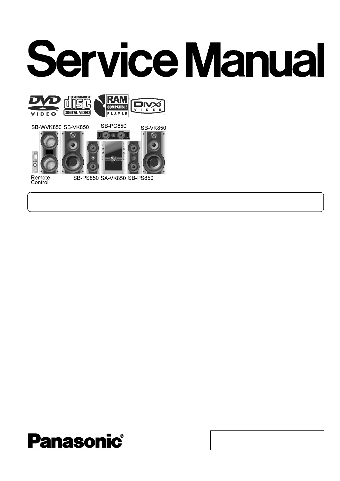
DVD Stereo System
SA-VK850EE
Colour
(S)... Silver Type
ORDER NO. MD0607234CE
Notes: This model’s DVD mechanism changer unit is CRS1D. Please refer to the original Service Manual
(Order No. MD0603065A3) for this mechanism.
Specifications
n AMPLIFIER SECTION
RMS Output Power: Dolby Digital Mode
Front - Ch
110 W per channel (3 Ω ), 1 kHz, 10% THD
Surround Ch
110 W per channel (3 Ω ), 1 kHz, 10% THD
Center Ch
110 W per channel (3 Ω ), 1 kHz, 10% THD
Subwoofer Ch
110 W per channel (3 Ω), 100 Hz, 10% THD
Total RMS Dolby Digital mode power
660 W
PMPO output power 7000 W
n FM/AM TUNER, TERMINALS SECTION
Preset stations FM 15 stations
AM 15 stations
Frequency Modulation (FM)
Frequency range
87.50 MHz to 108.00 MHz (50-kHz step)
Sensitivity 4.0 µV (IHF)
S/N 26 dB 2.2 µV
ntenna terminals 75 Ω (unbalanced)
mplitude Modulation (AM)
Frequency range 522 kHz to 1629 kHz (9-kHz step)
M sensitivity S/N 20 dB at 999 kHz
1000 µV/m
Phone jack
Terminal Stereo, 3.5-mm jack
Mic jack
Sensitivity 0.7 mV, 600 Ω
Terminal Mono, 6.3-mm jack (2 system)
Music Port jack (Front)
Sensitivity 100-mV, 4.7 kΩ
Terminal Stereo, 3.5-mm jack
n CASSETTE DECK SECTION
Type Auto Reverse
Track system 4-Track, 2 Channel
Head Record/Playback Solid permalloy head
Erasure Double Gap Ferrite Head
Motor DC Servo Motor
Recording system AC Bias 100 kHz
Erase System AC Erase 100 kHz
Tape Speed 4.8 cm/s
Overall Frequency Response (+3, -6 dB) at DECK OUT
Normal 35 Hz to 14 kHz
S/N Ratio 50 dB (A weighted)
Wow and Flutter 0.18% (WRMS)
Fast Forward and Rewind Time Approx. 120 seconds with
© 2006 Matsushita Electric Industrial Co. Ltd.. All
rights reserved. Unauthorized copying and
distribution is a violation of law.
Page 2
A
A
SA-VK850EE
C-60 cassette tape
n DISC SECTION
Disc played [8 cm or 12 cm]
(1) DVD (DVD-Video, DivX )
(2) DVD-RAM (DVD-VR, JPEG , MP3 , MPEG4 , DivX )
(3) DVD-R (DVD-Video, DVD-VR, JPEG , MP3 , MPEG4 ,
# 1,#2
DivX
)
#1,#2
#2,#3
#2,#4
#2,#3
#2,#4
#2,#5
#1,#2
#2,#5
(4) DVD-R DL (DVD-Video, DVD-VR)
(5) DVD-RW (DVD-Video, DVD-VR, JPEG , MP3 , MPEG4
2,#5
, DivX
# 1,#2
)
#2,#3
#2,#4
#
(6) +R/ +RW (Video)
(7) +R DL (Video)
#6
(8) CD,CD-R/RW [CD-DA, Video CD, SVCD , MP3 , WMA ,
JPEG
# 2,#3
, MPEG4
# 2,#5
, DivX
# 1,#2
, HighMAT Level 2 (Audio and
#2,#4
#2,#7
Image)]
#1
Plays all versions of DivX video (including DivX 6) with standard
® ®
playback of DivX®media files. Certified to the DivX Home Theater
Profile. GMC (Global Motion Compensation) is not supported.
#2
The total combined maximum number of recognizable audio,
picture and video contents and groups: 4000 audio, picture and video
contents and 400 groups.
#3
Exif Ver 2.1 JPEG Baseline files
Picture resolution: between 160 x 120 and 6144 x 4096 pixels
(Sub sampling is 4:0:0, 4:2:0, 4:2:2 or 4:4:4). Extremely long and
narrow pictures may not be displayed.
#4
MPEG-1 Layer 3, MPEG-2 Layer 3
#5
MPEG4 data recorded with the Panasonic SD multi cameras or
DVD video recorders.
Conforming to SD VIDEO specifications (ASF standard) / MPEG4
(Simple Profile) video system / G.726 audio system
#6
Conforming to IEC62107
#7
Windows Media Audio Ver. 9.0 L3
Not compatible with Multiple Bit Rate (MBR)
Pick up
Wavelength (DVD/CD) 662 nm/785 nm
Laser power (DVD/CD) CLASS 1 / CLASS 1M
udio output (Disc)
Number of channels (FL,FR,C,SL,SR,SW),5.1ch
udio performance (measurement at: Rec out terminal)
Frequency response (CD-Audio) 4Hzto20kHz
n VIDEO SECTION
Video system
Signal system PAL625/50, PAL525/60, NTSC
Composite video output
Output level 1Vp-p(75Ω)
Terminal Pin jack (1 system)
S-video output
Y output level 1Vp-p(75Ω)
C output level 0.3 Vp-p (75 Ω )(PAL)
0.286 Vp-p (75 Ω )(NTSC)
Terminal S terminal (1 system)
Component video output
[NTSC : 480p / 480i, PAL: 576p / 576i]
Y output level 1Vp-p(75Ω)
PBoutput level 0.7 Vp-p (75 Ω )
PRoutput level 0.7 Vp-p (75 Ω )
Terminal
Pin jack (Y: green, PB:blue,PR:red)(1system)
n GENERAL
Power supply AC 230 V, 50Hz
Power consumption 290 W
Power consumption in standby mode:
0.5 W (approximate)
Dimensions (W x H x D) 250 x 330 x 334.6 mm
Mass 5.5 kg
Operating temperatur e range +5to+35°C
Operating humidity range 5% to 90% RH (no condensation)
n SYSTEM
For information on speaker system, please refer to the original
Service Manual (Order No. MD0606210CE) for SB-VK850GC1-S,
(Order No. MD0606211CE) for SB-PS850GC-S, (Order No.
MD0606212CE) for SB-PC850GC-S & (Order No. MD0606213CE) for
SB-WVK850GC-S.
2
Page 3
Notes:
1. Specifications are subject to change without notice.
Mass and dimensions are approximate.
2. Total harmonic distortion is measured by the digital spectrum
analyzer.
SA-VK850EE
3
Page 4
SA-VK850EE
CONTENTS
Page Page
1 Safety Precautions 6
1.1. General Guidelines
1.2. Before Repair and Adjustment
1.3. Protection Circuitry
2 Prevention of Electro Static Discharge (ESD) to
Electrostatically Sensitive (ES) Devices
3 Handling Precautions for Traverse Unit
3.1. Handling Optical Pickup
3.2. Replacing Precautions for Optical Pickup Unit
3.3. Grounding for Preventing Electrostatic Destruction
4 Precaution of Laser Diode
5 Warning
5.1. Service caution based on legal restrictions
6 Accessories
7 Operation Procedures
7.1. Main Unit Operation Control
7.2. Remote Control Operation Control
7.3. Disc Information
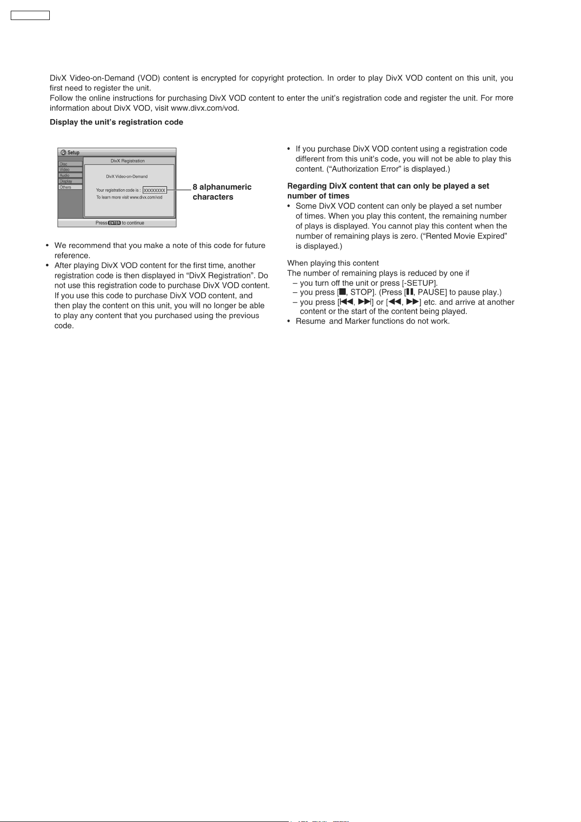
7.4. DivX VOD Content
8 New Features
8.1. CRS1D Mechanism Overview
8.2. Music Port
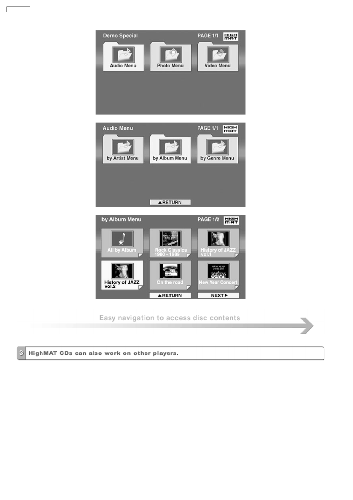
9 About HighMAT
9.1. What 痴 HighMAT?
9.2. Why take advantage of HighMAT?
9.3. Benefits of HighMAT?
10 Self diagnosis and special mode setting
10.1. Service Mode Summary Table
10.2. Service Mode Table 1
10.3. Special Mode Table 2
11 Assembling and Disassembling
11.1. Caution
11.2. Disassembly flow chart
11.3. Main Parts Location
11.4. Disassembly of Top Cabinet
11.5. Disassembly of CD/DVD Changer Unit (CRS1D)
11.6. Disassembly of Rear Panel
11.7. Disassembly of Main P.C.B.
11.8. Disassembly of Front Panel Unit
11.9. Disassembly of Digital Amp P.C.B.
11.10. Replacement for Power Amp IC (Digital Amp P.C.B.)
11.11. Disassembly of SMPS P.C.B.
11.12. Replacement of Power Amp IC (SMPS P.C.B.)
11.13. Disassembly of Panel P.C.B., Mic P.C.B. & Tact Switch
P.C.B.
10
10
11
12
12
13
14
16
17
17
19
20
20
20
21
24
24
24
32
40
40
41
42
43
43
44
45
45
46
46
47
47
48
6
6
6
7
8
8
8
8
9
11.14. Disassembly of Deck mechanism unit
11.15. Disassembly of Deck P.C.B.
11.16. Disassembly of Traverse Unit
11.17. Disassembly of optical pickup unit (CD/DVD mechanism )
11.18. Disassembly of Deck Mechanism
11.19. Replacement for cassette lid
11.20. Rectification for tape jam problem
12 Service Fixture and Tools
13 Service Positions
13.1. Checking and Repairing of Main P.C.B.
13.2. Checking and Repairing of SMPS P.C.B. & Digital Amp
P.C.B.
13.3. Checking and Repairing of Panel, Deck & Deck
Mechanism P.C.B.
14 Adjustment Procedures
14.1. Cassette Deck Section
14.2. Alignment Points
15 Voltage and Waveform Chart
15.1. DVD Module P.C.B.
15.2. Main P.C.B.
15.3. Panel P.C.B.
15.4. Deck P.C.B. & Deck Mechanism P.C.B.
15.5. Damp P.C.B. & Mic P.C.B.
15.6. Waveform Chart
16 Wiring Connection Diagram
17 Block Diagram
18 Notes of Schematic Diagrams
19 Schematic Diagram
19.1. Optical Pickup Unit Circuit
19.2. (A) DVD Module (DV3.2) Circuit
19.3. (B) Main Circuit
19.4. (C) Panel Circuit
19.5. (D) Tact Switch Circuit & (E) Mic Circuit
19.6. (F) Damp Circuit
19.7. (G) Speaker Circuit
19.8. (H) SMPS Circuit
19.9. (I) Deck Circuit & (J) Deck Mechanism Circuit
20 Printed Circuit Board
20.1. (A) DVD Module P.C.B. (Side A & B )
20.2. (B) Main P.C.B.
20.3. (C) Panel P.C.B.
20.4. (D) Tact Switch P.C.B., (E) Mic P.C.B., (I) Deck P.C.B. &
(J) Deck Mechanism, P.C.B.
20.5. (F) Damp P.C.B. & (G) Speaker P.C.B.
49
49
50
51
53
57
57
58
58
58
59
60
61
61
62
63
64
66
69
70
71
72
81
83
89
91
91
92
96
100
101
102
104
105
107
109
110
111
112
113
114
4
Page 5

SA-VK850EE
20.6. (H) SMPS P.C.B. 115
21 Basic Troubleshooting Guide for Backend Module
21.1. Firmware and Key Download
21.2. Initialisation and Playability
22 Illustration of ICs, Transistors and Diodes
23 Terminal Function of IC
117
117
117
118
119
23.1. IC2600 (C2CBYY0 00269) System Microprocessor
24 Exploded Views
24.1. Cabinet Parts Location
24.2. Deck Mechanism Parts Location (RAA3413-1S)
24.3. Packaging
25 Replacement Parts List
119
121
121
123
124
129
5
Page 6
SA-VK850EE
1 Safety Precautions
1.1. General Guidelines
1. When servicing, observe the original lead dress. If a short circuit is found, replace all parts which have been overheated or
damaged by the short circuit.
2. After servicing, see to it that all the protective devices such as insulation barriers, insulation papers shields are properly
installed.
3. After servicing, make the following leakage current checks to prevent the customer from being exposed to shock hazards.
1.1.1. Leakage Current Cold Check
1. Unplug the AC cord and connect a jumper between the two prongs on the plug.
2. Measure the resistance value, with an ohmmeter, between the jumpered AC plug and each exposed metallic cabinet part on
the equipment such as screwheads, connectors, control shafts, etc. When the expose d metallic part has a return path to the
chassis, the reading should be between 1MΩ and 5.2MΩ.
When the exposed metal does not have a return path to the chassis, the reading must be
.
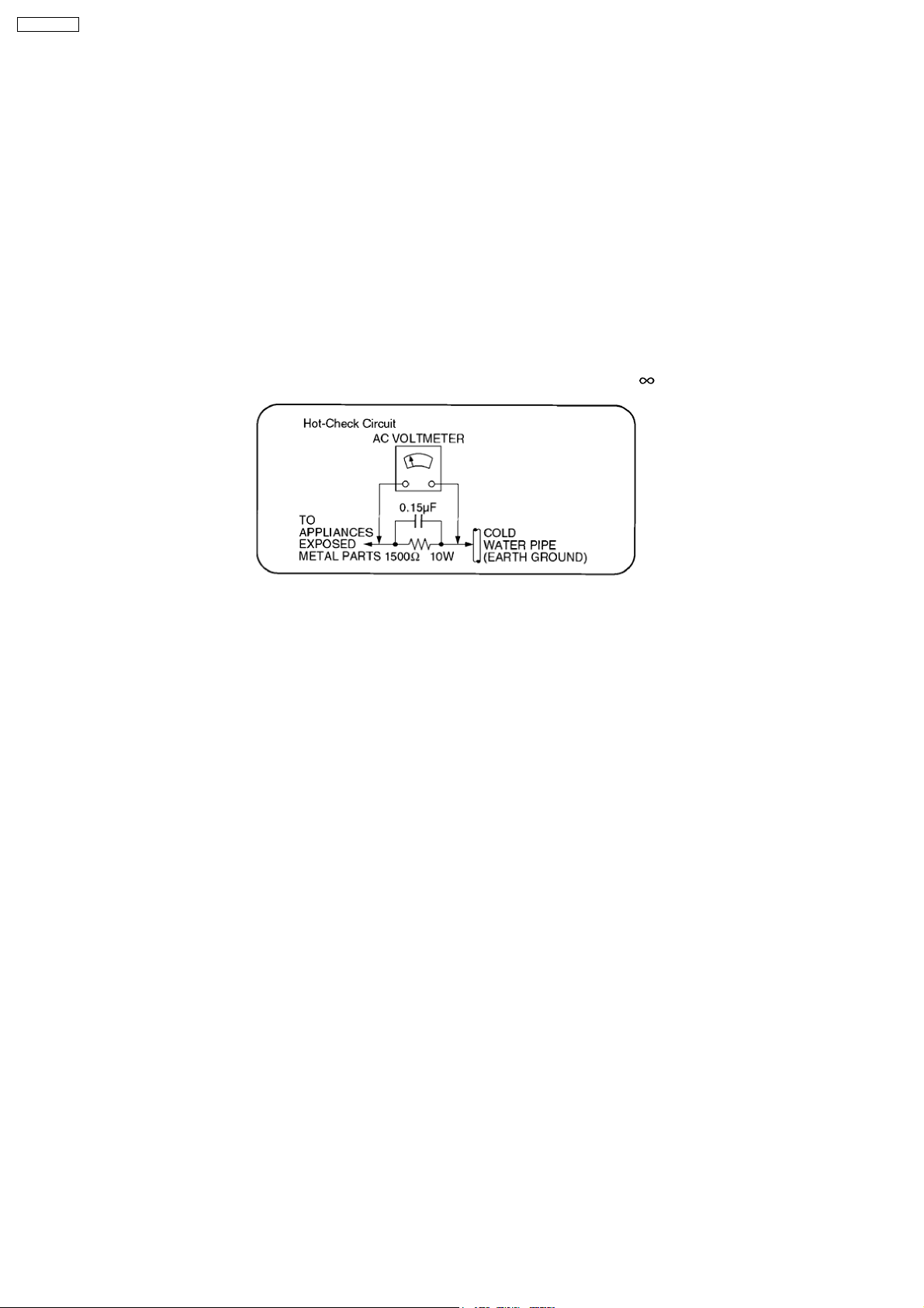
Figure 1
1.1.2. Leakage Current Hot Check
(See Figure 1)
1. Plug the AC cord directly into the AC outlet. Do not use an isolation transformer for this check.
2. Connect a 1.5kΩ, 10 watts resistor, in parallel with a 0.15µF capacitor, between each exposed metallic part on the set and a
good earth ground such as a water pipe, as shown in Figure 1.
3. Use an AC voltmeter, with 1000 ohms/volt or more sensitivity, to measure the potential across the resistor.
4. Check each exposed metallic part, and measure the voltage at each point.
5. Reverse the AC plug in the AC outlet and repeat each of the above measurements.
6. The potential at any point should not exceed 0.75 volts RMS. A leakage current tester (Simpson Model 229 or equivalent) may
be used to make the hot checks, leakage current must not exceed 1/2 milliamp. In case a measurement is out of the limits
specified, there is a possibility of a shock hazard, and the equipment should be repaired and rechecked before it is returned to
the customer.
1.2. Before Repair and Adjustment
Disconnect AC power, discharge Power Supply Capacitors C2254, C2256, C2288, C2289, C2632, C2721, C2725, C2811, C2815,
C2817, C5512, C5513, C5514, C5712, C5713, C5715, C5805 , C5806, C5807, C5914 , C5916 , C5917 , C5929 , C5930, C5971 and
C5977 through a 10Ω, 5W resistor to ground.
DO NOT SHORT-CIRCUIT DIRECTLY (with a screwdriver blade, for instance), as this may destroy solid state devices.
After repairs are completed, restore power gradually using a variac, to avoid overcurrent.
Current consum ption at AC 230V, 50Hz in NO SIGNAL (vol. min, at CD mode) should be ~500mA.
1.3. Protection Circuitry
The protection circuitry may have operated if either of the following conditions are noticed:
· No sound is heard when the power is turned on.
· Sound stops during a performance.
The function of this circuitry is to prevent circuitry damage if, for example, the positive and negative speaker connection wires are
“shorted”, or if speaker systems with an impedance less than the indicated rated impedance of the amplifier are used.
If this occurs, follow the procedure outlines below:
6
Page 7
SA-VK850EE
1. Turn off the power.
2. Determine the cause of the problem and correct it.
3. Turn on the power once again after one minute.
Note :
When the protection circuitry functions, the unit will not operate unless the power is first turned off and then on again.
2 Prevention of Electro Static Discharge (ESD) to
Electrostatically Sensitive (ES) Devices
Some semiconducto r (solid state) devices can be damaged easily by electricity. Such components commonly are called
Electrostatically Sensitive (ES) Devices. Examples of typical ES devices are integrated circuits and some field-effect transistors and
semiconductor “chip” components. The following techniques should be used to help reduce the incidence of component damage
caused by electro static discharge (ESD).
1. Immediately before handling any semiconductor component or semiconductor-equipped assembly, drain off any ESD on your
body by touchin g a known earth ground. Alternatively, obtain and wear a commercially available discharging ESD wrist strap,
which should be removed for potential shock reasons prior to applying power to the unit under test.
2. After removing an electrical assembly equipped with ES devices, place the assembly on a conductive surface such as
aluminium foil, to prevent electrostatic charge build up or exposu re of the assembly.
3. Use only a grounded-tip soldering iron to solder or unsolder ES devices.
4. Use only an anti-static solder remover device. Some solder removal devices not classified as “anti-static (ESD protected)” can
generate electrical charge to damage ES devices.
5. Do not use freon-propelled chemicals. These can generate electrical charges sufficient to damage ES devices.
6. Do not remove a replacement ES device from its protective package until immediately before you are ready to install it. (Most
replacement ES devices are packaged with leads electrically shorted together by conductive foam, aluminium foil or
comparable conductive material).
7. Immediately before removing the protective material from the leads of a replacement ES device, touch the protective material
to the chassis or circuit assembly into which the device will be installed.
Caution
Be sure no power is applied to the chassis or circuit, and observe all other safety precautions.
8. Minimize body motions when handling unpackaged replacement ES devices. (Otherwise harmless motion such as the brushing
together of your clothes fabric or the lifting of your foot from a carpeted floor can generate static electricity (ESD) sufficient to
damage an ES device).
7
Page 8
SA-VK850EE
3 Handling Precautions for Traverse Unit
The laser diode used inside optical pickup could be destroyed due to static electricity as a potential difference is caused by
electrostatic load discharged from clothes or human body. Handling the parts carefully to avoid electrostatic destruction during
repair.
3.1. Handling Optical Pickup
1. Do not impact on optical pickup as the unit structurally uses an extremely precise technology.
2. Short-circuit the flexible cable of optical pickup remove from the circuit board using a short-circuit pin or clip in order to prevent
laser diode from electrostatic destruction (Refer to Fig. 3.1 and Fig. 3.2)
3. Do not handle flexible cables forcibly as this may cause snapping. Handle the parts carefully (Refer to Fig. 3.1)
4. A new optical pickup is equipped with an anti-static flexible cable. After replacing and connecting to the flexible board, cut the
anti-static flexible cable. (Refer to Fig. 3.1)
Fig 3.1
3.2. Replacing Precautions for Optical Pickup Unit
CD/DVD Optical Pickup
The optical pickup by which part supply was carried out attaches the short clip to the flexible board for laser diode electrostatic
discharge damage prevention. Please remove the short clip and be sure to check that the short land is open, before connecting.
(Please remove solder, when the short land short-circuits.)
3.3. Grounding for Preventing Electrostatic Destruction
1. Human body grounding
Use the anti-static wrist strap to discharge the static electricity accumulated in your body. (Refer to Fig. 3.2)
2. Work place grounding
Place a conductive material (conductive sheet) or ironboard where optical pickup is placed. (Refer to Fig. 3.2)
Note :
Keep your clothes away from optical pickup as wrist strap does not release the static electricity charged in clothes.
Fig. 3.2
8
Page 9
SA-VK850EE
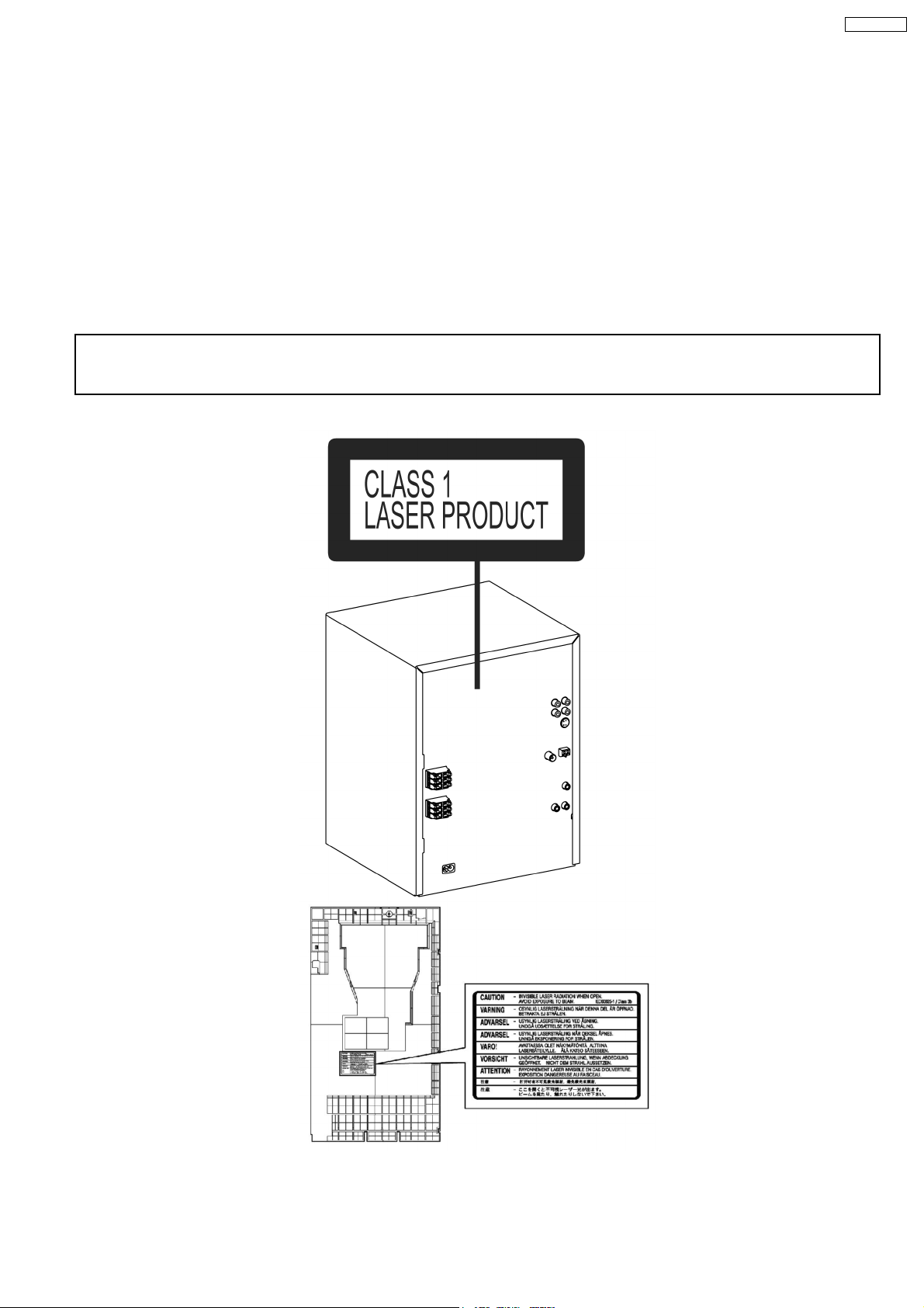
4 Precaution of Laser Diode
Caution :
This product utilizes a laser diode with the unit turned "ON", invisible laser radiation is emitted from the pick up lens.
Wavelength : 785 nm(CD)/662 nm(DVD)
Maximum output radiation power from pick up : 100 µW/VDE
Laser radiation from pick up unit is safety level, but be sure the followings:
1. Do not disassemble the optical pick up unit, since radiation from exposed laser diode is dangerous.
2. Do not adjust the variable resistor on the pick up unit. It was already adjusted.
3. Do not look at the focus lens using optical instruments.
4. Recommend not to look at pick up lens for a long time.
CAUTION!
THIS PRODUCT UTILIZES A LASER.
USE OF CONTROLS OR ADJUSTMENTS OR PERFORMANCE OF PROCEDURES OTHER THAN THOSE SPECIFIED HEREIN MAY RESULT
IN HAZARDOUS RADIATION EXPOSURE.
n Use of Caution Labels
9
Page 10

SA-VK850EE
5 Warning
5.1. Service caution based on legal restrictions
5.1.1. General description about Lead Free Solder (PbF)
The lead free solder has been used in the mounting process of all electrical components on the printed circuit boards used for this
equipment in considering the globally environmental conservation.
The normal solder is the alloy of tin (Sn) and lead (Pb). On the other hand, the lead free solder is the alloy mainly consists of tin
(Sn), silver (Ag) and Copper (Cu), and the melting point of the lead free solder is higher approx.30 degrees C (86°F) more than that
of the normal solder.
Definition of PCB Lead Free Solder being used
The letter of “PbF” is printed either foil side or components side on the PCB using the lead free solder.
(See right figure)
Service caution for repair work using Lead Free Solder (PbF)
· The lead free solder has to be used when repairing the equipment for which the lead free solder is used.
(Definition: The letter of “PbF” is printed on the PCB using the lead free solder.)
· To put lead free solder, it should be well molten and mixed with the original lead free solder.
· Remove the remaining lead free solder on the PCB cleanly for soldering of the new IC.
· Since the melting point of the lead free solder is higher than that of the normal lead solder, it takes the longer time to melt
the lead free solder.
· Use the soldering iron (more than 70W) equipped with the temperature control after setting the temperature at 350±30
degrees C (662±86°F).
Recommended Lead Free Solder (Service Parts Route.)
· The following 3 types of lead free solder are available through the service parts route.
RFKZ03D01K-----------(0.3mm 100g Reel)
RFKZ06D01K-----------(0.6mm 100g Reel)
RFKZ10D01K-----------(1.0mm 100g Reel)
Note
* Ingredient: Tin (Sn), 96.5%, Silver (Ag) 3.0%, Copper (Cu) 0.5%, Cobalt (Co) / Germanium (Ge) 0.1 to 0.3%
10
Page 11
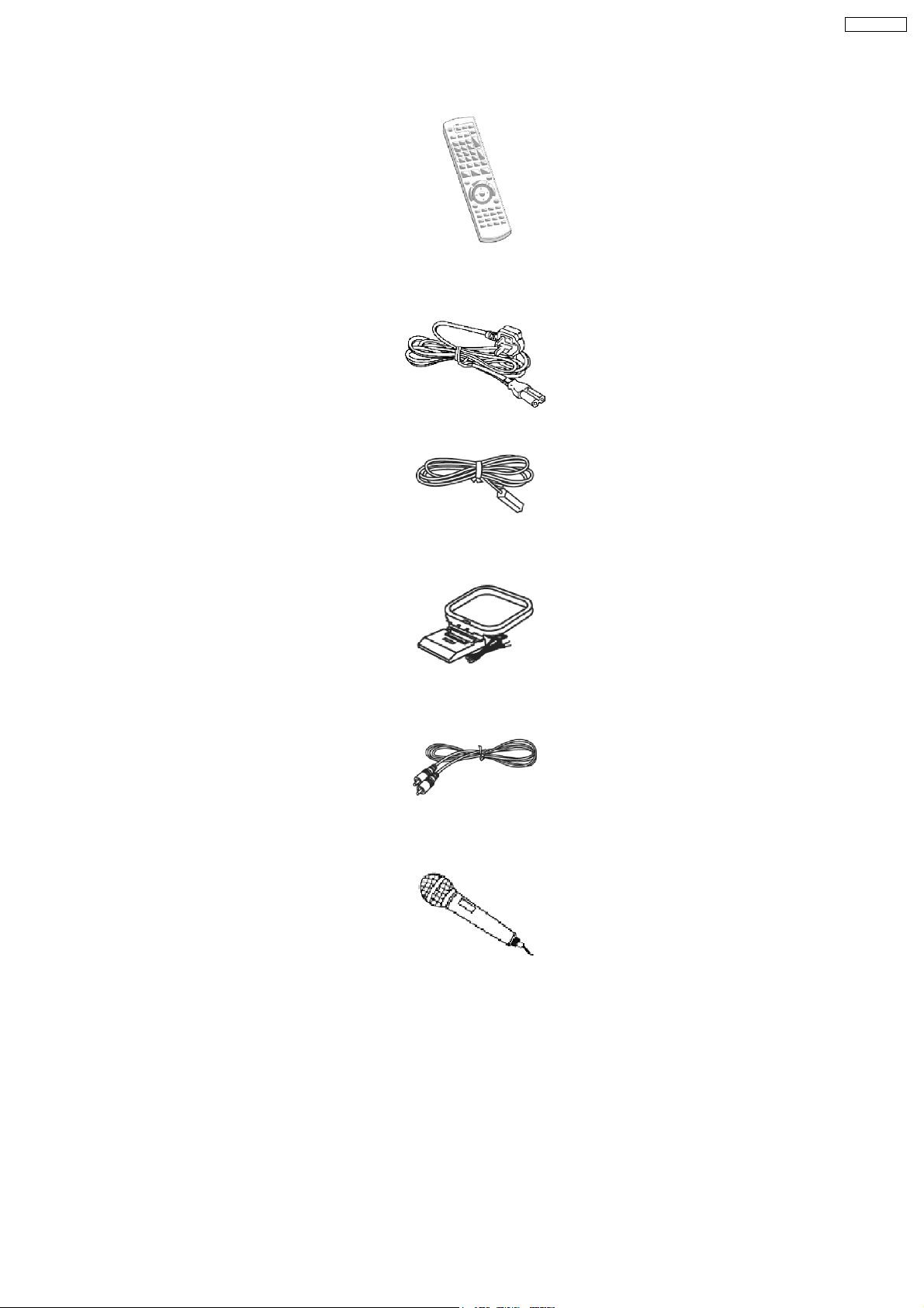
6 Accessories
SA-VK850EE
Remote
control
AC power supply cord
FM indoor antenna
AM loop antenna
Video cable
Microphone
11
Page 12

SA-VK850EE
7 Operation Procedures
7.1. Main Unit Operation Control
12
Page 13
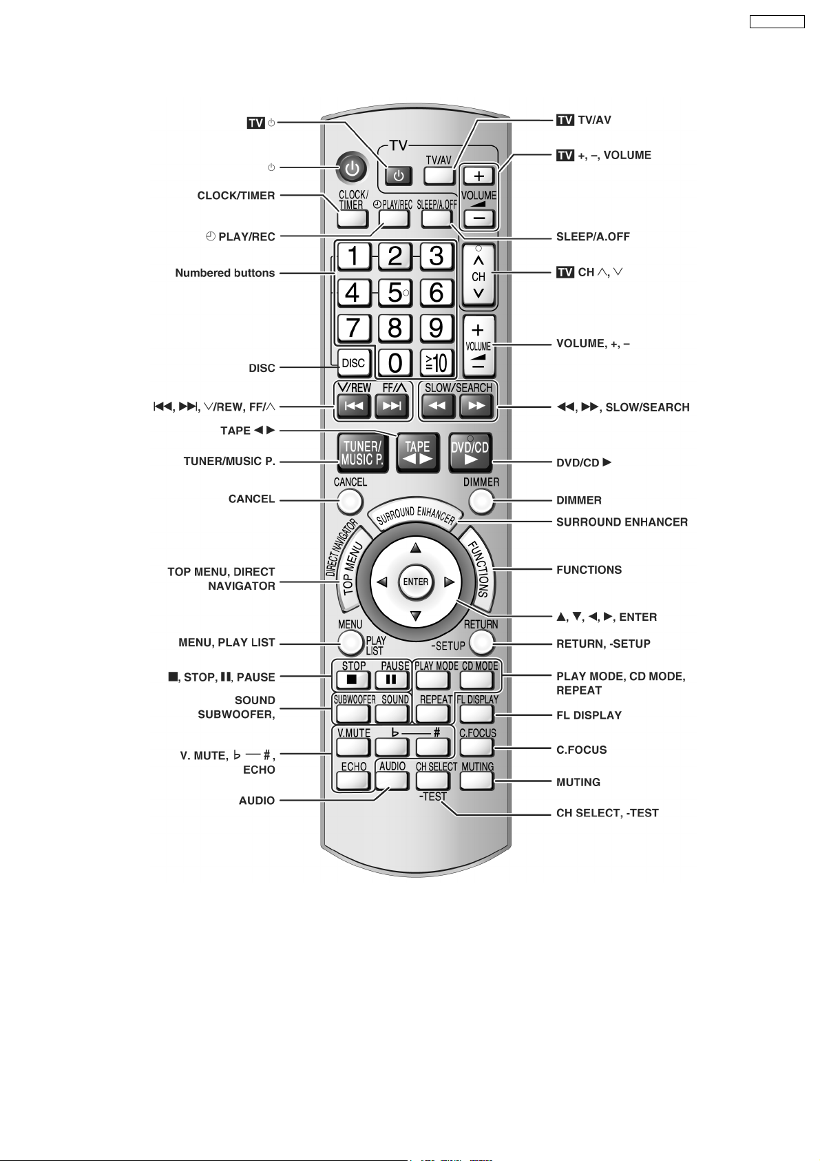
7.2. Remote Control Operation Control
SA-VK850EE
13
Page 14
SA-VK850EE
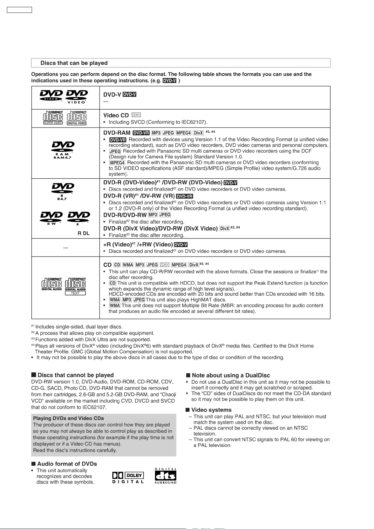
7.3. Disc Information
7.3.1. Disc Playability
14
Page 15
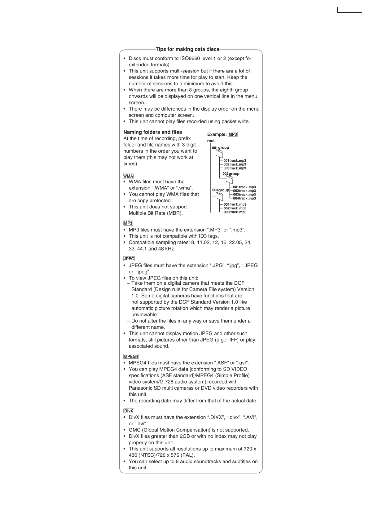
7.3.2. To Play MP3/ WMA and still Pictures (JPEG/ tiff)
SA-VK850EE
15
Page 16
SA-VK850EE
7.4. DivX VOD Content
16
Page 17
8 New Features
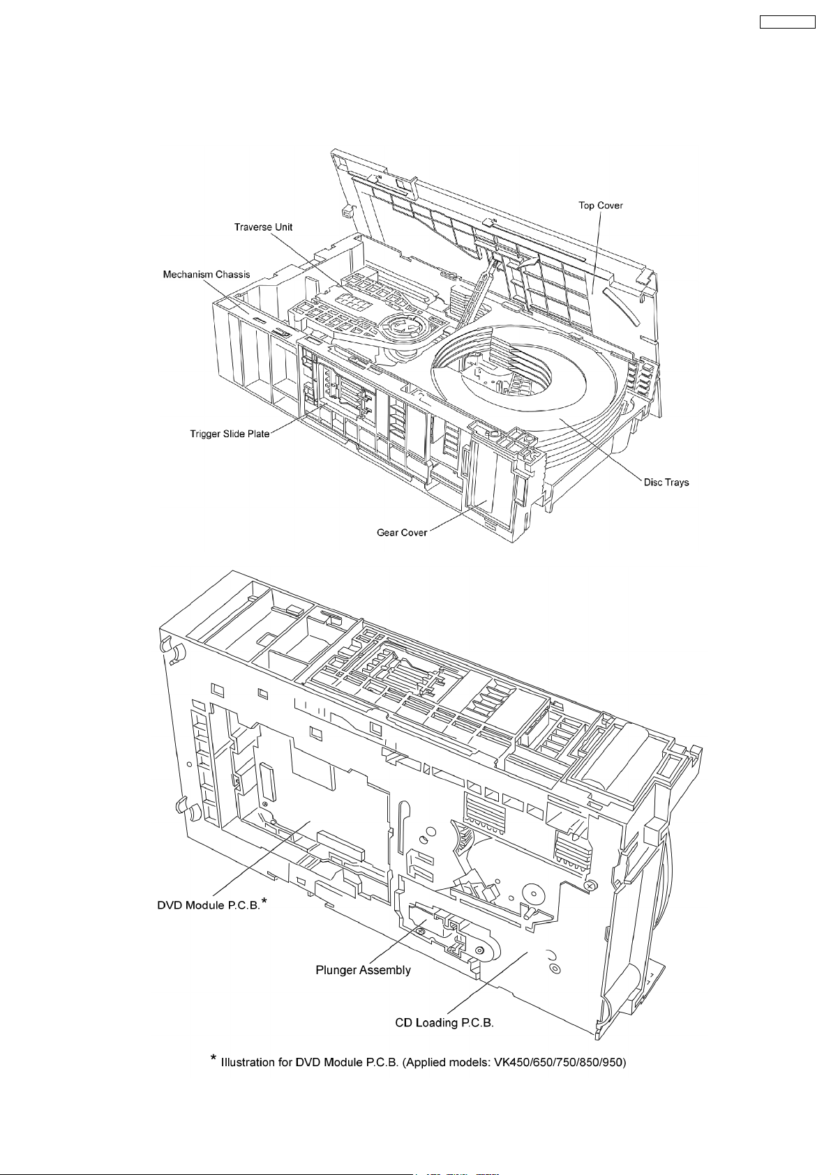
8.1. CRS1D Mechanism Overview
SA-VK850EE
17
Page 18

SA-VK850EE
8.1.1. General Feature
· This is a five disc changer mechanism for CD/DVD. The outline figure is shown below.
· The mechanism has "CHANGE WHILE PLAY" function. It open other trays for disc exchan ging while one tray is at PLAY
position performing recording or reproducing.
· The mechanism can quickly change all trays with "CHANGE ALL" function. All trays can be move to OPEN position with one
operation.
· There is no sensor to indicate presence of disc on any tray.
8.1.2. Hardware composition
· Below is the hardware components of the mechanism
Name Function
Open Switch (OPEN-SW) The switch is used to detect normal tray opening
The switch is used for detect tray being manually push/trigger when full open
Home Switch (HOME-SW) Is used to detect cam gear home position
Close Sensor (CLOSE-SENSOR) Used for normal single tray closing
Used to detect cam gear rotate to Play Driving position
Play Switch (PLAY-SW) Detect TRV clamping complete position
Stocking Switch (STOCK-SW) Detect tray completely transfer for play position to stocking position
UD Sensor (UD-SENSOR) Detect TRV vertical movement position
Top Switch (TOP-SW) Detect a default position of TRV vertical movement position
Driver IC To drive Motor
Motor Main driving source for changer
Plunger Switching the driving source from motor to:
1. Tray open/close
2. Drive tray to play/stock position and TRV vertical movement
8.1.3. Mechanism Operation
· This mechanism has the following state:
1. Driving of a tray to open/close
2. Up/down operation of a traverse performs a state changes of tray.
By using the plunger to lift/release of a switching gear, and the cam gear to lift/release the function gear the motor can be link
to several gear trains to perform various operations.
· The functions that can be perform in this mechanism are described as below:
Condition Explanation
Open current playing tray The state to change current playing disc. All tray will be open at once and current tray at PLAY position
Open All The state where all trays being driven to OPEN position. The disc can be taken in or out from tray to tray
Stock The state where the trays are stored in STOCK position
Play The state where one of the tray 5 trays is being driven to PLAY position and clamped by traverse unit
Play & Open Tray-* The state where one of the tray is in playing position performing recording or reproducing, other trays can
will be expose.
by close tray one by one from top to bottom.
be used (OPEN position) for disc exchanging without stopping the recording or reproducing process.
18
Page 19
Condition Explanation
Change The state when one of the opened tray being driven from OPEN position to STOCK position and other
opened trays remain still at OPEN position.
Close All The state where all open trays will being driven from OPEN position to STOCK position, one by one from
top to bottom
Note: * represent tray number (from 1 ~ 5)
8.1.4. New CD/DVD Mechanism (CRS1D)
Note:
This service manual does not contain the following information for the mention CD/DVD Mechanism drive:
· Schematic Diagram, Block Diagram and P.C.B. layout of CD/DVD Loading P.C.B.
· Part List for individual parts of the mechanism.
· Explode d View and Parts List for individual parts of the CD/DVD Mechanism drive.
Please refer to the original service manual (Order No. MD0603065A3) for the CD/DVD Mechanism Drive CRS1D.
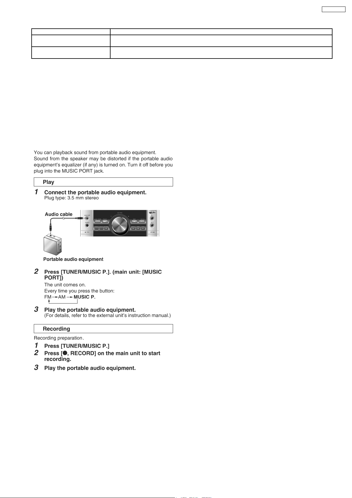
8.2. Music Port
SA-VK850EE
With reference to page 31 of the operating instruction manual.
19
Page 20

SA-VK850EE
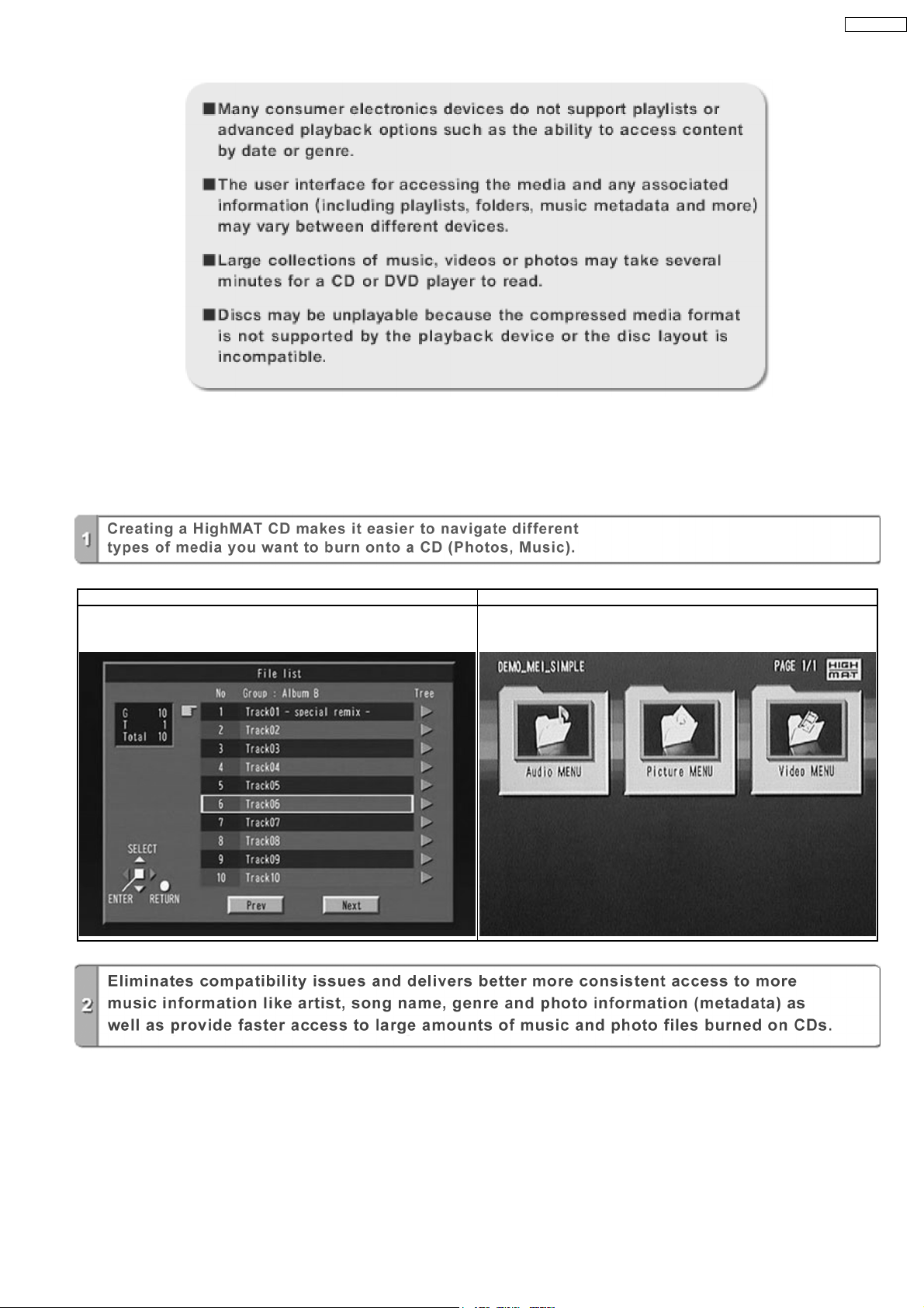
9 About HighMAT
9.1. What’s HighMAT?
Consumers worldwide are using PCs to create their own collections of music, photos and even video by burning them onto CDs.
But how these collections can be experienced across different devices can be confusing to navigate, time consum ing to access for
a DVD player, and be incomplete in terms of music information available to the customer.
HighMAT offers a solution to this growing consumer problem. HighMAT dramatically improves the digital media experience on
consumer electronic devices by delivering a simple, standardized approach that allows consumers who have created personal
collections of digital music, photography and video on their PC to:
>> Create a HighMAT CD or DVD which can be easily played back on consum er electronics devices such as CD and DVD players ,
and car stereos.
>> Move digital media files (using recordable media such as CD-R and CD-RW) between the PC and various playback devices
such as CD and DVD players.
A new standard for creating personal media on consumer electronic devices, HighMAT enable easier and more seamless
interoperability between Windows PCs and devices designed for your living room, or the car.
9.2. Why take advantage of HighMAT?
A Problem Defined:Toda y, when consumers create their own digital audio, video or photo collections on CD-R or other physical
formats, there are numerous, inconsistent ways that devices read the data. For the consumer, the playba ck experie nce can be
confusing:
20
Page 21
SA-VK850EE
A Solution Created: HighMAT delivers a better digital media access experience by creating a standard approach for PCs to
structure digital media on various physical formats and for playback devices to read the data.
9.3. Benefits of HighMAT?
Conventional HighMAT
Even though DVD player is CD-R/RW compatible, the inconsistent ways
that various DVD players can read the music or photos files often leads
to a confusing and inconsistant playback experince.
HighMAT compatible products play content back with consistent
interface. This includes products which are JPEG compatible products
without HighMAT support.
21
Page 22
SA-VK850EE
22
Page 23
SA-VK850EE
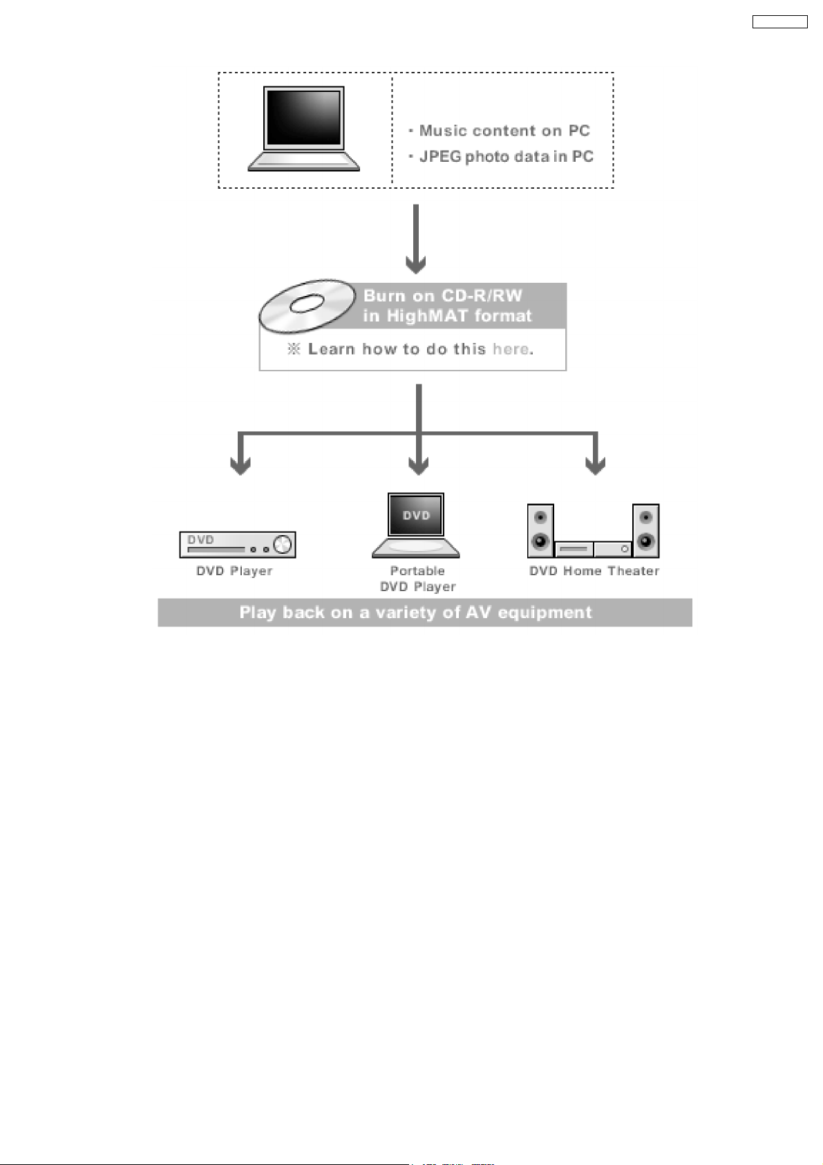
HighMAT is now available for CD Burning and in Leading DVD PlayersHighMAT is a new technology that is now available in leading
software and consumer electronic devices to dramatically improve the digital media experience when you create homemade
CDsHighMAT delivers a simple, standardized way for PC software and consumer electronics devices to talk to each other and work
better together.
When you create your homemade CDs with software that supports HighMAT CD burning, and then play them back on a DVD
player that supports HighMAT, you get better, easier navigation. You get folders you can access with a single click of your DVD
player´s remote control. You can view important information about your music like full song names, artist titles, album names and
genre. And you can get faster startup on your home entertainment device.
To enjoy the benefits of HighMAT, all you need is software that supports HighMAT for CD burning of music or photos, as well as
a home entertainment device like a DVD player that supports HighMAT for playback. Always look for the HighMAT logo on your
software or home entertainment device to ensure it supports the HighMAT experience.
23
Page 24
SA-VK850EE
10 Self diagnosis and special mode setting
This unit is equipped with functions for checking and inspecting namely: Self-Diagnostic and Test Mode.
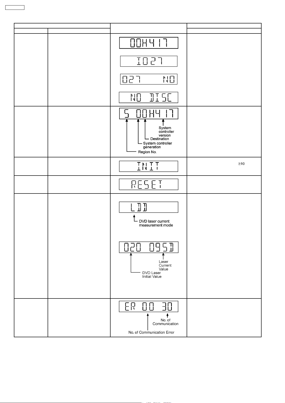
10.1. Service Mode Summary Table
The service modes can be activated by pressing various button combination on the player and remote control unit.
Below is the summary of major checking:
Player buttons Remote control unit buttons Application Note
STOP 0 Error code display (Refer to the section,
5 Jitter checking (Refer to the section
6 Region display and mode (Refer to the section
7 Micro-processor firmware version check
FUNCTIONS DVD laser drive current check
3 CD laser drive current check
Initial setting of laser drive current
“10.2.2 DVD Self
Diagnostic Function-Error
Code”).
“10.2.1 Service Mode
Table 1 for more
information”).
“10.2.1 Service Mode
Table 1 for more
information”).
Initialization of the player (factory setting is restored.)
Used after replacement of micro-computer, FLASH ROM IC,
EEPROM and HDMI module.
8 Region and Firmware version display
ENTER DVD Module Reset (In Initialization Mode)
10.2. Service Mode Table 1
By pressing various button combin ations on the player and remote control unit can activate the various service modes for checking.
Special Note:
Due to the limitations of the no. characters that can be shown on FL Display, the “FL Display” button on the remote control unit
is used to show the following page. (Display 1 / Display 2).
10.2.1. Service Mode Table 1
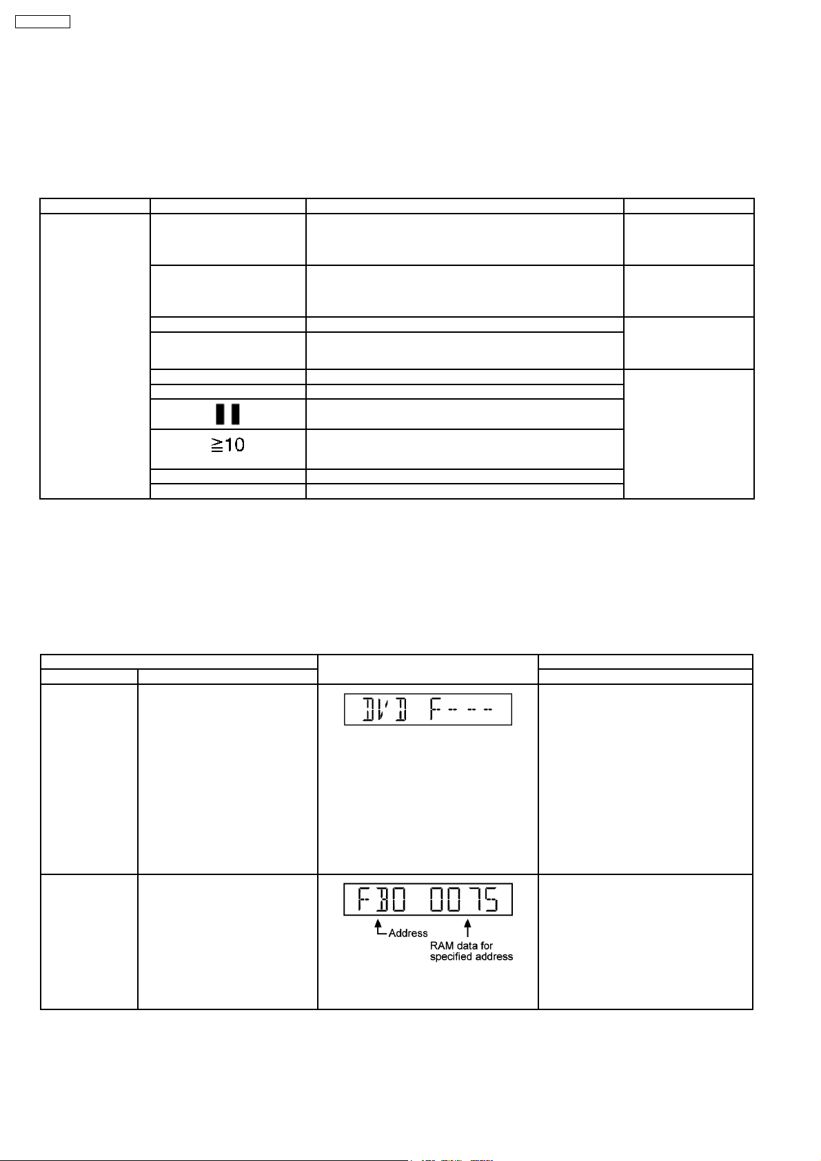
Item FL Display Key Operation
Mode Name Description Remote Control Key
Error code check Error code check.
ADSC internal
RAM data check
The latest error code stored in the
EEPROM IC is displayed.
ADSC internal RAM data check.
ADSC internal RAM data is read
out and displayed.
Error code (play_err) is expressed in the
following convention.
Error code = 0 x DAXX is expressed: DVDnn
UXX
Error code = 0 x DBXX is expressed: →
DVDnn HXX
Error code = 0 x DXXX is expressed: →
DVDnn FXXX
Error code = 0 x 0000 is expressed: →
DVDnn F--* “xx” denotes the error code →
In STOP (no disc) mode, press STOP
button on the player, and “0” button on the
remote control unit. *With pointing of cursor
up and down on display.
Cancelled automatically 5 seconds later.
To exit, press [POWER] button on main
unit or remote control.
In STOP (no disc) mode, press STOP
button on the player, and “1” or “2” button
on the remote control unit.
Press STOP or PLAY button to exit.
The value is shown in hexadecimal notation.
The above example shows the data in
ADSC address OFAh is 6901h.
24
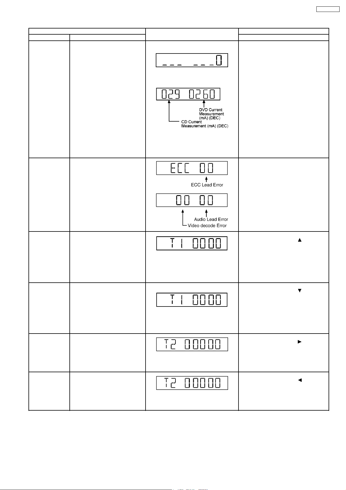
Page 25
Item FL Display Key Operation
Mode Name Description Remote Control Key
CD laser drive
current
measurement
CD laser drive current
measurement.
CD laser drive current measured
and the result is displayed together
with the initial value stored in the
EEPROM IC.
1. For CD laser drive current mode
In STOP (no disc) mode, press STOP
button on the player, and “3” button on the
remote control unit.
Cancelled automatically 5 seconds later.
Press “FL Display” button on remote
control unit for next page (FL Display).
After the measurement, CD laser
emission is kept on. It is turned off
when POWER key is switched off.
(It is also turned off when POWER
button on the player is switched
2. The measurement Value (In decimal
notation)
off.)
SA-VK850EE
Device Name Display the device name. 1.
2.
3.
Jitter check Jitter check.
1. For jitter measurement mode
Jitter rate is measured and
displayed.
Measurement is repeatedly done in
the cycle of one second. Read
error counter starts from zero upon
mode setting. When target block
data failed to be read out, the
counter advances by one
increment. When the failure is
caused by minor error, it may be
2.
corrected when retired to enable
successful reading. In this case,
the counter advances by one.
When the error persists even after
retry, the counter may jump by two
or more.
In STOP (no disc) mode, press STOP
button on the player, and “4” button on the
remote control unit. *With pointing of cursor
up and down on display.
Cancelled automatically 5 seconds later.
To exit, press [POWER] button on main
unit or remote control.
In STOP (no disc) mode, press STOP
button on the player, and “5” button on the
remote control unit.
Press STOP or OPEN button to exit.
Press “FL DISPLAY” button on remote
control unit for next page (FL Display).
Jitter rate is shown in decimal notation to
one place of decimal.
Focus drive value is shown in hexadecimal
notation.
Region display Region display & mode In STOP (no disc) mode, press STOP
button on the player, and “6” button on the
remote control unit.
Cancelled automatically 5 seconds later.
25
Page 26
SA-VK850EE
Item FL Display Key Operation
Mode Name Description Remote Control Key
Micro- processor
firmware version
display &
EEPROM
checksum display.
Micro-processor firmware version
display & EEPROM checksum
display.
In STOP (no disc) mode, press STOP
button on the player, and “7” button on the
remote control unit.
Cancelled automatically 5 seconds later.
Press “FL Display” button on remote
control unit for next page. (FL Display)
Refer to Section 10.3.1 for more
information.
DVD module
firmware version
DVD module firmware version
display is on the FL Display.
display
Initialization Initialization.
User settings are cancelled and
player is initialized to factory
setting.
DVD Module
Reset
To reset DVD Module.
In initialisation when the FLASH
ROM IC or DVD Module is
replaced.
DVD laser drive
current
measurement
DVD laser drive current
measurement.
DVD laser drive current is
measured and the result is
displayed together with the initial
value stored in the EEPROM IC.
After the measurement, DVD laser
emission is kept on. It is turned off
when POWER key is switched off.
(It is also turned off when POWER
button on the player is switched
off.)
1. For DVD laser drive current mode
2. The measurement value (In decimal
notation)
In STOP (no disc) mode, press STOP
button on the player, and “8” button on the
remote control unit.
Cancelled automatically 5 seconds later.
In STOP (no disc) mode, press STOP
button on the player, and
button
on the remote control unit.
In initialisation mode, press and hold STOP
button on the player followed by “Enter”
button on the remote control.
Cancelled automatically 5 seconds later.
In STOP (no disc) mode, press STOP
button on the player, and FUNCTIONS
button on the remote control unit.
Cancelled automatically 5 seconds later.
Press “FL Display” button on remote
control unit for next page (FL Display) on
values of DVD drive current.
Communication error display
Displays the frequency of
communication errors between
system control IC and mechanism
control IC.
The value denotes the current in decimal
notation.
The above example shows the initial current
is 20mA and the measured value is 20mA.
In STOP (no disc) mode, press STOP
button on the player, and “MENU” button
on the remote control unit.
Cancelled automatically 5 seconds later.
26
Page 27
SA-VK850EE
Item FL Display Key Operation
Mode Name Description Remote Control Key
Initial setting of
laser drive current
Initial setting of laser drive current.
Initial current value for each of
DVD laser and CD laser is
separately saved in the EEPROM
IC.
1. For DVD/CD drive current mode
2. The measurement value (In decimal
notation)
In STOP (no disc) mode, press STOP
button on the player, and PAUSE button on
the remote control unit.
Cancelled automatically 5 seconds later.
Press “FL Display” button on remote
control unit for next page (FL Display) on
values of laser drive current.
The value denotes the current in decimal
notation. The above example shows the
initial current 20mA and 23mA for DVD
laser and CD laser respectively when the
laser is switched on.
ECC error display ECC decode error display. In STOP (no disc) mode, press STOP
button on the player, and TOP MENU
button on the remote control unit.
Cancelled automatically 5 seconds later.
Press “FL Display” button on remote
control unit for next page (FL Display) on
values of laser drive current.
Time 1 check Timer 1 check.
Laser operation time is measured
separately for DVD laser and CD
laser.
Press “FL Display” button for next
page of FL Display (to show CD
laser time).
Timer 1 reset Timer 1 reset.
Laser operation time of both DVD
laser and CD laser is reset all at
once.
Timer 2 check Timer 2 check.
Spindle motor operation timer.
Press “FL Display” button for next
page of FL Display.
Timer 2 reset Timer 2 reset.
Spindle motor operation timer.
Shown to the left is DVD laser time, and to
the right CD laser time.
Time is shown in 4 digits of decimal notation
in a unit of 10 hours.
“0000” will follow “9999”.
T1_0000/0000 (display1/display2)
Shown to the left is DVD laser time, and to
the right CD laser time.
Time is shown in 4 digits of decimal notation
in a unit of 10 hours.
Time is shown in 5 digits of decimal notation
in a unit of 10 hours.
“0000” will follow “9999”.
Time is shown in 5 digits of decimal notation
in a unit of 10 hours.
It clears to “0000” upon reset.
In STOP (no disc) mode, press STOP
button on the player, and “
” button on
the remote control unit.
Cancelled automatically 5 seconds later.
While display Timer 1 data, press STOP
button on the player, and “
“ button on
the remote control unit.
Cancelled automatically 5 seconds later.
In STOP (no disc) mode, press STOP
button on the player, and “
“ button on
the remote control unit.
Cancelled automatically 5 seconds later.
While display Timer 2 data, press STOP
button on the player, and “
“ button on
the remote control unit.
Cancelled automatically 5 seconds later.
27
Page 28
SA-VK850EE
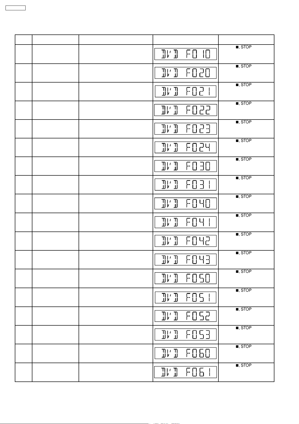
10.2.2. DVD Self-Diagnostic Function Error Code
Error
Code
F010 DVD Media disk A specification value is size from the
F020 DVD Media disk There is no TT_SRPT. (RLBN is 0). Press [ ] on main
F021 DVD Media disk The number of TT_SRP is 0. Press [ ] on main
F022 DVD Media disk A specification value. It is size from the
F023 DVD Media disk VTSN or in agreement with VTS_TTN.
F024 DVD Media disk A specification value. It is size from
F030 DVD Media disk The number of TTU_SRP is 0. Press [ ] on main
F031 DVD Media disk A specification value. It is size from the
Diagnosis Contents Description of error Automatic FL Display Remarks
PARENTAL LOCK value of the
appointed country.
number of TT_SRP.
There is no SRP.
TT_SRP. PTT_Ns
number of TTU_SRP.
Press [ ] on main
unit for next error.
unit for next error.
unit for next error.
Press [ ] on main
unit for next error.
Press [ ] on main
unit for next error.
Press [ ] on main
unit for next error.
unit for next error.
Press [ ] on main
unit for next error.
F040 DVD Media disk The number of SRP1 is 0. Press [ ] on main
F041 DVD Media disk The number of PGCI_SRP is 0. Press [ ] on main
F042 DVD Media disk A specification value. It is size from the
number of PGCI_SRP.
F043 DVD Media disk It is in agreement with Menu ID. There is
no PGCI_SRP.
F050 DVD Media disk The number of TMAP_SRP is 0. Press [ ] on main
F051 DVD Media disk A specification value. It is size from the
number of TMAP_SRP.
F052 DVD Media disk Specification TMAP_SA is 0. Press [ ] on main
F053 DVD Media disk The number of MAP_EN is 0. Press [ ] on main
unit for next error.
unit for next error.
Press [ ] on main
unit for next error.
Press [ ] on main
unit for next error.
unit for next error.
Press [ ] on main
unit for next error.
unit for next error.
unit for next error.
F060 DVD Media disk Although C_POSIT exists, it is in PGC.
There is no PGMAP.
F061 DVD Media disk Although C_POSIT exists, it is in PGC.
There is no PGMAP.
28
Press [ ] on main
unit for next error.
Press [ ] on main
unit for next error.
Page 29
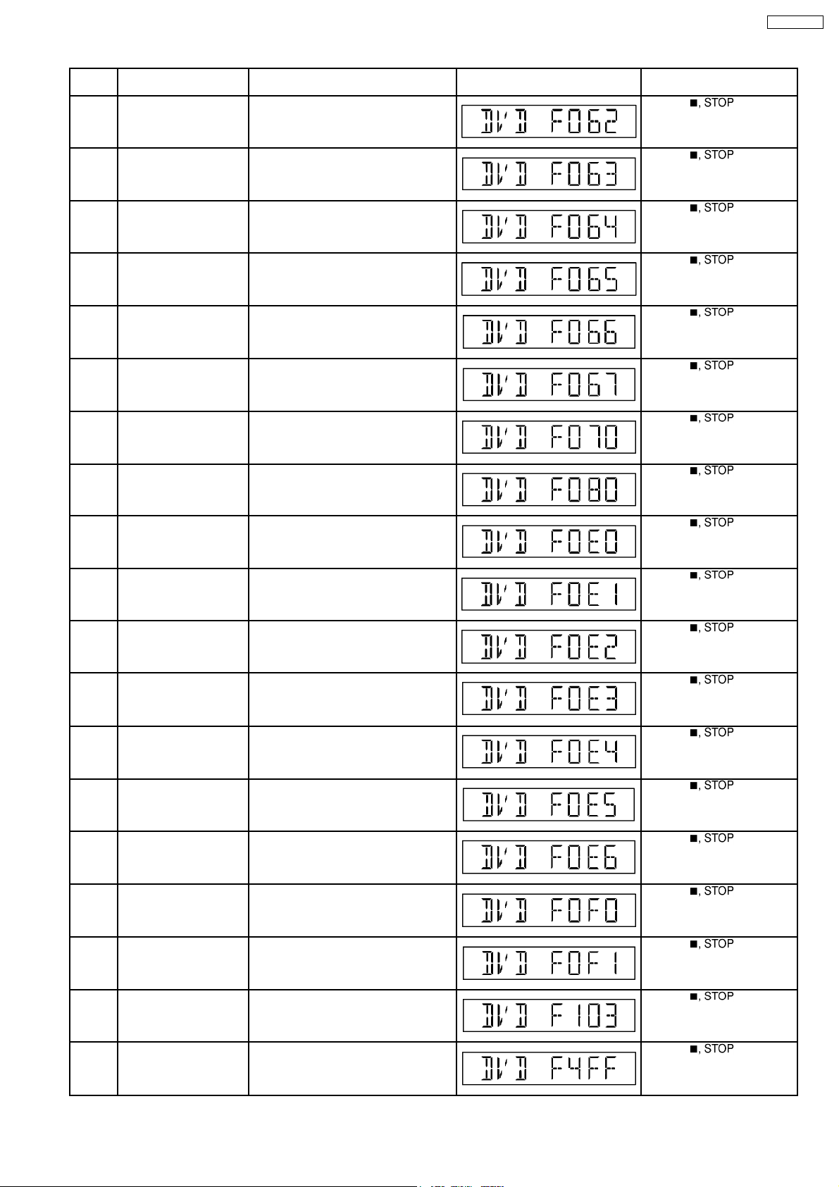
SA-VK850EE
Error
Diagnosis Contents Description of error Automatic FL Display Remarks
Code
F062 DVD Media disk A specification value inside of PGC. It is
size from the number of PGes.
F063 DVD Media disk Although C_POSIT exists, it is in PGC.
There is no C_PBIT.
F064 DVD Media disk Although C_POSIT exists, it is in PGC.
The number of PGes is 0.
Press [ ] on main
unit for next error.
Press [ ] on main
unit for next error.
Press [ ] on main
unit for next error.
F065 DVD Media disk Specification A cell number is 0.‘ Press [ ] on main
unit for next error.
F066 DVD Media disk A specification value inside of PGC. It is
size from the number of Cell(s).
Press [ ] on main
unit for next error.
F067 DVD Media disk A blocked cell is present. Press [ ] on main
unit for next error.
F070 DVD Media disk There is no NV_PACK data. Press [ ] on main
unit for next error.
F080 DVD Media disk Under reference. There is no Cell
number.
Press [ ] on main
unit for next error.
F0E0 DVD Media disk For [used as a DFD object] a user guide.
A PGC control file < impossible.
F0E1 DVD Media disk DFD main microcomputer. Compatibility
with a DFD type < download is
Press [ ] on main
unit for next error.
Press [ ] on main
unit for next error.
impossible.
F0E2 DVD Media disk DFD download start. PGC reproduction
error.
F0E3 DVD Media disk Waiting for the completion of DFD
download. PGC reproduction error.
Press [ ] on main
unit for next error.
Press [ ] on main
unit for next error.
F0E4 DVD Media disk At the time of DFD download AVDEC. Press [ ] on main
unit for next error.
F0E5 DVD Media disk It is the farm file lead error at the time of
DFD download.
F0E6 DVD Media disk DFD alteration check error of the read
firmware.
F0F0 DVD Media disk There is no farm file used as a DFD
object and it is downloading needlessly.
Press [ ] on main
unit for next error.
Press [ ] on main
unit for next error.
Press [ ] on main
unit for next error.
F0F1 DVD Media disk The firware which is in agreement with
DFD download conditions <
unnecessary.
F103 Illegal highlight Position Big possibility of disc specification
violation during highlight display
F4FF Force initialize failure
Timeout when force initialization fails Press [ ] on main
(time out)
29
Press [ ] on main
unit for next error.
Press [ ] on main
unit for next error.
unit for next error.
Page 30
SA-VK850EE
Error
Diagnosis Contents Description of error Automatic FL Display Remarks
Code
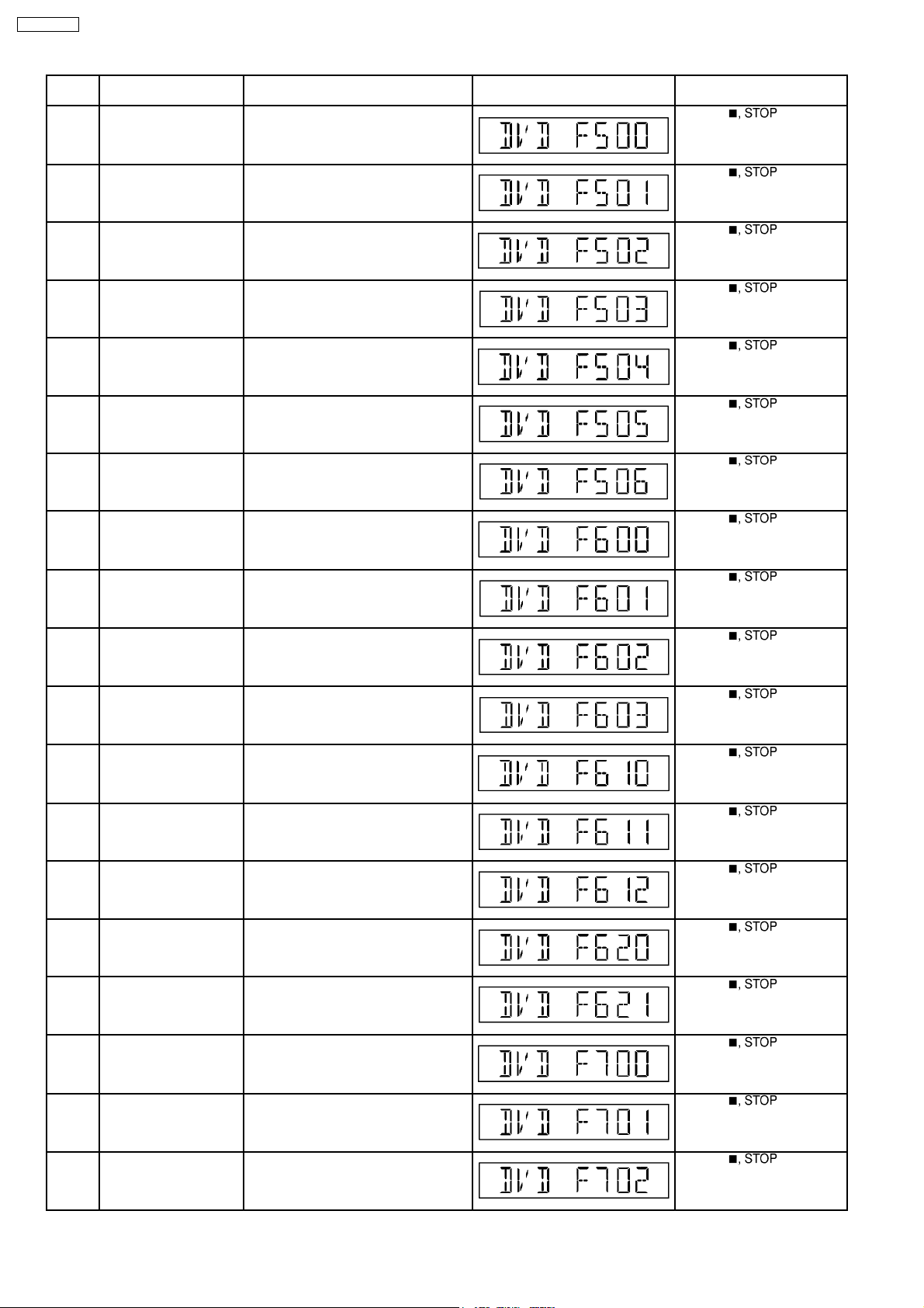
F500 DSC error DSC (IC8251) stops in the occurrence of
servo error (startup, focus error, etc.)
F501 DSC not Ready error DSC-system computer communication
error (Communication failure caused by
Press [ ] on main
unit for next error.
Press [ ] on main
unit for next error.
idling of DSC)
F502 DSC Time out error Similar as F500 Press [ ] on main
unit for next error.
F503 DSC communication
Failure
Communication error (result error
occurred although communication
Press [ ] on main
unit for next error.
command was sent)
F504 Abnormal adjusting DSC
data slice offset
Press [ ] on main
unit for next error.
F505 DSC Attention error Similar as F500 Press [ ] on main
unit for next error.
F506 Invalid media Disc is flipped over, TOC unreadable,
incompatible disc media
F600 Access failure to
management information
caused by demodulation
Operation stopped because navigation
data is not accessible caused by the
demodulation defect
Press [ ] on main
unit for next error.
Press [ ] on main
unit for next error.
error
F601 Indeterminate sector ID
requested
Operation stopped caused by the
request to access abnormal ID data
Press [ ] on main
unit for next error.
F602 Access failure to LEAD-
IN caused by
LEAD IN data unreadable Press [ ] on main
unit for next error.
demodulation error
F603 Access failure to
KEYDET caused by
Access failure to CSS data of disc Press [ ] on main
unit for next error.
demodulation error
F610 ODC abnormality No permission for command execution Press [ ] on main
unit for next error.
F611 No CRC OK for a
specific time (CD)
F612 No CRC OK for a
specific time (DVD)
F620 Laser safeguard: high
temperature condition
F621 Laser safeguard: circuit
failure condition
Access failure to seek address in CD
series
Press [ ] on main
unit for next error.
Access failure to ID data in DVD series Press [ ] on main
unit for next error.
High temperature of the laser guide unit
(OPU unit)
Circuitry failure of the laser guide unit
(OPU unit)
Press [ ] on main
unit for next error.
Press [ ] on main
unit for next error.
F700 MBX overflow When replying message to disc manager Press [ ] on main
unit for next error.
F701 Message command
does not end
F702 Message command
changes
Next message is sent before replying to
disc manager
Message is changed before it is sent as
a reply to disc manager
30
Press [ ] on main
unit for next error.
Press [ ] on main
unit for next error.
Page 31

SA-VK850EE
Error
Code
F880 Task number is not
F890 Sending message when
F891 Message couldn’t be
F893 FLASH ROM IC problem FLASH ROM IC installed is not operating
F894 EEPROM abnormality EEPROM IC installed is not operating in
F895 Region setting
F896 No existence model Firm version agreement check for factory
F897 Initialize is not
Diagnosis Contents Description of error Automatic FL Display Remarks
appropriate
message is being sent to
AV task
sent to AV task
abnormality
completed
Message coming from a non-existing
task
Sending message to AV task Press [ ] on main
Begin sending message to AV task Press [ ] on main
properly (Neccessary replacement of
FLASH ROM IC) or firmware problem
normal condition (EEPROM contains
neccessary data)
Firm version agreement check for factory
preset setting failure prevention. Check
region setting & re-initialize
preset setting failure prevention
Initialize completion check for factory
preset setting failure prevention
Press [ ] on main
unit for next error.
unit for next error.
unit for next error.
Press [ ] on main
unit for next error.
Press [ ] on main
unit for next error.
Press [ ] on main
unit for next error.
Press [ ] on main
unit for next error.
Press [ ] on main
unit for next error.
F898 Disagreement of
hardware and software
F8A0 Message command is
not appropriate
Unsuitable combination of AV
DECORDER, SDRAM and FLASH ROM
(firmware)
Message command is not suitable Press [ ] on main
Press [ ] on main
unit for next error.
unit for next error.
Note:
An error code will be canceled if a power supply is turned OFF.
*1: CPPM is the copy guard function beforehand written in the disk for protection of copyrights.
10.2.3. Optical Pickup Breakdown Diagnosis
This unit is equipped with the optical pickup self-diagnosis function and the tilt adjustment check function. Follow the procedure
described below during repair in order to perform self-diagnosis and tilt adjustment effectively. Especially when “NO DISC” is
displayed, be sure to apply the self-diagnosis function before replacing with an optical pickup. Replacement of optical pickup
generally requires when the present value of laser drive exceeds 45 (DVD) or 45 (CD).
Note:
Start diagnosis within three minutes after turning on the power (as diagnosis fails when the unit becomes warm).
31
Page 32

SA-VK850EE
10.3. Special Mode Table 2
Item FL Display Key Operation
Mode Name Description Front Key
Self -Diagnostic
Mode
CD Changer
Reliability Test
(CRS1D)
To enter into self
diagnostic checking for
main unit.
To determine the
reliability of CD/DVD
Changer Unit. (For more
infomation, refer to
section 10.3.2.)
1. Select [ ] for DVD/CD mode.
2. Press and hold [
To exit, press
unit or remote control.
In Self-Diagnostic Mode:
1. Select [
2. Press [1] on remote control..
To exit, press
unit or remote control.
(The tray will return to PLAY position and then
power off)
32
(Ensure no disc is inserted into the drive
unit.)
] button for 3
seconds follow by [
] for CD mode.
].
button on main
button on main
Page 33

Item FL Display Key Operation
Mode Name Description Front Key
Doctor Mode To enter into “Doctor
Mode” for purpose of
checking various
functions of the main unit
(Example: Micro-p
Firmware version &
EEPROM IC check etc)
1. FL will light up for all segments
2. Device display
3.
4. In doctor mode (under CD mode)
In CD mode:
1. Press [
To exit, press [ENTER] button on remote
control or
or remote control.
Note: In firmware version & checksum data
(EEPROM IC) displayed when the buttons is
pressed twice.
SA-VK850EE
] button on main unit
follow by [4] and [7] on remote control.
(Ensure no disc is inserted into drive unit.)
button on main unit
Cold Start Initialize backup data and
FL Display Test To check the FL
Tape Eject Test To check on the tape
Firmware version
check &
EEPROM IC
Information
Firmware version
checking (For
DVD Module)
start the micro-processor.
segments display (All
segments will light up and
LED will blink at 0.5
second interval)
eject function (For deck
1/2)
To display the microprocessor firmware
version & checksum date
when there is an
EEPROM IC istalled
To display the firmware
version for the DVD
Module
(Firmware is loaded to
FLASH ROM IC)
1. All segments will light up for 1 second.
In doctor mode:
1. Press [4] on remote control.
To exit, press [ENTER] button on remote
control or
or remote control.
In doctor mode:
1. Press
control.
Both deck will be eject automatically. In doctor mode:
1. Press [0] button on remote control.
1. Firmware version display & the EEPROM. In doctor mode:
1. Press [
follow by [4] and [7] on remote control.
To exit, press [ENTER] button on remote
control or
or remote control.
Refer to Section 10.3.1 for more information.
In doctor mode:
1. Press [
follow by [CANCEL] on remote control.
To exit, press [ENTER] button on remote
control or
or remote control.
button on main unit
button on remote
] button on main unit
button on main unit
] button on main unit
button on main unit
10.3.1. EEPROM Checksum (ROM Correction)
Purpose: To check for microprocessor firmware version and EEPROM checksum (ROM correction).
Below are the procedures for this mode.
Step 1: Enter into Doctor mode (for more information, refer to section 10.3 on the key operation to enter into this mode.
Step 2: Check for firmware version and EEPROM checksum (By pressing STOP button on main unit followed by “4” and “7” on
remote control).
· W hen entering into DOCTOR MODE, the firmware version and checksum data of EEPROM (if applicable) will appear on FL
33
Page 34

SA-VK850EE
display. Below is the information on the EEPROM IC (ROM correction) under 3 possible situations:
1. In the case that the correction point existence data is other than 0 (ie. correction file exists), EEPROM checksum display for
the microprocessor shall be made after calculating checksum by summing up the content of data area from EEPROM IC.
2. In the case when no EEPROM IC is installed. It is display as below (no display of checksum data)
3. In cases that the filename is different even though a EEPRO M is installed, or no correction file exists, [NG] shall be display ed
(the correction point existence data is set to 0 at this condition).
Note: Microprocessor firmware refers to version number for microprocessor IC located on PANEL P.C.B.. It is subject to change
which would be update d accordingly. ROM correction checksum refers to the HEX code that is displayed upon key buttons pressed
if an EEPROM is loaded in the unit.
10.3.2. CD/DVD changer unit ageing test mode
Below is the process flow chart of ageing for the CD/DVD changer unit. (CRS1D)
34
Page 35

SA-VK850EE
35
Page 36

SA-VK850EE
10.3.3. Error Code Table
Self-Diagnosis Function (refer Section 10.3) provides information on any problems occuring for the unit and its respective
components by displaying the error codes. These error code such as U**, H** and F** are stored in memory and held unless it is
cleared.
The error code is automatically display after entering into self-diagnostic mode.
Error Code Diagnosis Contents Description of error Automatic FL Display Remarks
H01 Mode SW, plunger
and capstan motor
abnormal
H02 Rec INH SW
abnormal
H03 HALF SW abnormal (Traverse motor,
F15 RESET SW
abnormal
F26 Transmission error
between CD Servo
LSI IC and
microprocessor IC
The tray is not able to
open.
(Spindle servo, DSC
(IC8251) Spindle motor,
CLV servo error)
IC8251)
REST SW: ON is not
detected within the
specified time.
When set to CD mode,
the sense signal does
not turn “Low”, a fail safe
time after system
command transmission
is sent.
For deck mechanism unit (For deck 1/2).
Press [
next error.
For deck mechanism unit (For deck 2).
Press [
next error.
For deck mechanism unit (For deck 1/2).
Press [
next error.
For DVD unit (For Traverse).
Press [
next error.
For DVD unit (For Traverse).
Press [
next error.
] on main unit for
] on main unit for
] on main unit for
] on main unit for
] on main unit for
36
Page 37

Error Code Diagnosis Contents Description of error Automatic FL Display Remarks
F61 Power Amp IC output
abnormal
Upon power on,
PCONT=HIGH,
DCDET=L after checking
For power.
Press [
next error.
LSI.
IHMS Cam gear
abnormality
Cam gear does not
rotate to “HOME”
position.
For CD/DVD changer unit (CRS1D).
Press [SINGLE CHANGE] on main unit
for next error.
SA-VK850EE
] on main unit for
ICSL Cam gear/gear units
abnormal
Cam gear does not
rotate to “PLAY” driving
position and hence does
not drive playing tray to
“STOCK” position.
ISTK Drive rack/gear
assembly abnormal
The tray drive rack does
not move to “STOCK”
position. (Tray does not
move to “STOCK”
position)
IPLY Drive rack/gear
assembly abnormal
The tray drive rack does
not move to “PLAY”
position. (Tray does not
move to “PLAY” position)
ITOP UD assembly UD Rack does not move
to front direction. This
lead to UD base not
raise to top position.
For CD/DVD changer unit (CRS1D).
Press [SINGLE CHANGE] on main unit
for next error.
For CD/DVD changer unit (CRS1D).
Press [SINGLE CHANGE] on main unit
for next error.
For CD/DVD changer unit (CRS1D).
Press [SINGLE CHANGE] on main unit
for next error.
For CD/DVD changer unit (CRS1D).
Press [SINGLE CHANGE] on main unit
for next error.
IUDS UD assembly After TOP SW is
detected, UD rack does
not move into tray 1
position.
HOME Cam gear/gear
assembly abnormal
Cam gear does not
move to “HOME”
position under following
conditions
1. After tray is load to
“PLAY” position.
2. After tray is unload
to “STOCK” position.
For CD/DVD changer unit (CRS1D).
Press [SINGLE CHANGE] on main unit
for next error.
For CD/DVD changer unit (CRS1D).
Press [SINGLE CHANGE] on main unit
for next error.
37
Page 38

SA-VK850EE
Error Code Diagnosis Contents Description of error Automatic FL Display Remarks
LOAD Tray drive assembly
abnormal
Tray unit does not move
from “STOCK” to “PLAY”
position
For CD/DVD changer unit (CRS1D).
Press [SINGLE CHANGE] on main unit
for next error.
PDRV Cam gear/gear
assembly abnormal
UDU UD base asssembly
abnormal
UDD UD base asssembly
abnormal
UD1 UD base asssembly
abnormal
F1NG Fail - safe mode. (For
open/close tray
unit(s))
Cam gear does not
move from “HOME” to
“PLAY” drive position.
UD Base assembly does
not move upwards from
tray 5 to tray 2
UD Base assembly does
not move downwards
from tray 1 to tray 5.
UD Base assembly does
not move to tray 1.
When the tray open
operation is performed, it
fails to open. It will
automatically close all
trays after the time-out
by the microprocessor.
During this time when it
fails, the error code will
appear.
For CD/DVD changer unit (CRS1D).
Press [SINGLE CHANGE] on main unit
for next error.
For CD/DVD changer unit (CRS1D).
Press [SINGLE CHANGE] on main unit
for next error.
For CD/DVD changer unit (CRS1D).
Press [SINGLE CHANGE] on main unit
for next error.
For CD/DVD changer unit (CRS1D).
Press [SINGLE CHANGE] on main unit
for next error.
For CD/DVD changer unit (CRS1D).
Press [SINGLE CHANGE] on main unit
for next error.
F2NG Fail - safe mode. (For
open/close tray
unit(s))
SRVC_TRV To unlock the
traverse unit for
service
RSET Cam gear jam/close
sensor faulty
When the tray close
operation is performed, it
fails to close. It will
automatically open all
trays after the time-out
by the microprocessor.
During this time when it
fails, the error code will
appear.
1. All trays set to
“STOCK” position
2. Mechanism set to
tray 5
3. Cam gear set to
“HOME” position
During tray re-open, the
cam gear will rotate in
the opposite direction to
reset the cam gear
position. When it fails,
the error code will
appear.
For CD/DVD changer unit (CRS1D).
Press [SINGLE CHANGE] on main unit
for next error.
For CD/DVD changer unit (CRS1D).
Press [SINGLE CHANGE] on main unit.
For CD/DVD changer unit (CRS1D).
Press [SINGLE CHANGE] on main unit
for next error.
CRS1D Error Code display
1. The errors that occured in CRS1D Mechanism can be recalled and displayed, in the order of the occurence under selfdiagnostic (Refer to Section 10.3 for procedures to enter this mode.
· Only the first 5 errors will be memorized (in backup memory). The subsequence error shall be ignored and not memorize.
38
Page 39

For system with EEPROM as memory backup,memory space in EEPROM is neccesary.
2. To display all error code memorized
In CRS1D Self-Diagnostic mode, press [SINGLE CHANGE] to display subsequence error code.
It shall repeat after reaching error no. 5.
e.g.:
[1____IHMS]→ [SINGLE CHANGE]
[2____ITOP]→ [SINGLE CHANGE]
[3____HOME]→ [SINGLE CHANGE]
[4____LOAD]→ [SINGLE CHANGE]
[5_____UDD]→ [SINGLE CHANGE]
3. To clear the error code memory
In CRS1D Self-Diagnostic mode, long press [SINGLE CHANGE] key (2s or more)
SA-VK850EE
39
Page 40

SA-VK850EE
11 Assembling and Disassembling
11.1. Caution
Special Note:
This model uses a new CD/DVD changer unit CRS1D. In this following section does not contain the necessary disassembly &
assembly information for the CD/DVD changer unit (CRS1D) except the disasembly & assembly of traverse unit. Kindly refer
to the original service manual for the CD/DVD changer unit. (Order No. MD0603065A3).
“ATTENTION SERVICER”
Some chassis components may have sharp edges. Be carefu l when disassembling and servicing.
1. This section describes procedures for checking the operation of the major printed circuit boards and replacing the main
components.
2. For reassembly after operation checks or replacement, reverse the respective procedures.
Special reassembly procedures are described only when required.
3. Select items from the following index when checks or replacement are required.
4. Refer to the Parts No. on the page of “Parts Location and Replacement Parts List” (Section 25), if necessary.
Warning :-
This product uses a laser diode. Refer to caution statement Precaution of Laser Diode.
Caution:
After replacing of CD/DVD Changer Unit, ageing test is necessary. Please confirm operation for CD/DVD Changer Unit.
Below is the list of disassembly sections
· Disasse mbly of Top Cabinet
· Disasse mbly of CD/DVD Changer Unit
· Disasse mbly of Rear Panel
· Disasse mbly of Main P.C.B.
· Disasse mbly of Front Panel Unit
· Disasse mbly of Digital Amp P.C.B.
· Replacement for Power Amp IC (Digital Amp P.C.B.)
· Disasse mbly of SMPS P.C.B.
· Replacement of Power Amp IC (SMPS P.C.B.)
· Disasse mbly of Panel P.C.B., Mic P.C.B. & Tact Switch P.C.B.
· Disasse mbly of Deck Mechanism Unit
· Disasse mbly for Deck P.C.B.
· Disasse mbly of Traverse Unit
· Disasse mbly of Optical Pickup Unit (CD/DVD Mechanism)
· Disasse mbly of Deck Mechanism
· Replacement for cassette lid
· Rectification for tape jam problem
40
Page 41

SA-VK850EE
11.2. Disassembly flow chart
The following chart is the procedure for disassembling the casing and inside parts for internal inspection when carrying out the
servicing.
To assemble the unit, reverse the steps shown in the chart as below.
41
Page 42

SA-VK850EE
11.3. Main Parts Location
42
Page 43

11.4. Disassembly of Top Cabinet
Step 1 Remove 3 screws at each side and 5 screws at rear
panel.
Step 2 Lift up both sides of the top cabinet, push the top
cabinet towards the rear to remove the top cabinet.
SA-VK850EE
11.5. Disassembly of CD/DVD Changer Unit (CRS1D)
· Follow the (Step 1) - (Step 2) of Item 11.4 - Disassembly of Top Cabinet
Step 1 Remove 2 screws at rear panel.
Step 2 Detach the FFC cables (CN2038 & CN2036).
Step 3 Release the claws on both ends.
Step 4 Lift the CD/DVD changer unit upwards to remove it.
43
Page 44

SA-VK850EE
· Disasse mbly of Mecha Chassis
Step 5 Remove 2 screws.
Step 6 Remove the Mecha Chassis.
Note:
For disassembly & assembly of traverse unit, please refer to
section 11.16 of this service manual. Please refer to original
Service Manual for the Disassembly and Assembly of the
CD/DVD Changer Unit (CRS1D), section 5.
11.6. Disassembly of Rear Panel
· Follow the (Step 1) - (Step 2) of Item 11.4 - Disassembly of Top Cabinet
· Follow the (Step 1) - (Step 4) of Item 11.5 - Disassembly of CD/DVD Changer Unit
Step 1 Remove 8 screws.
Step 2 Remove 2 screws at Speaker P.C.B..
Step 3 Detach the fan wires CNP2913 from Main P.C.B..
Step 4 Remove rear panel.
44
Page 45

11.7. Disassembly of Main P.C.B.
· Follow the (Step 1) - (Step 2) of Item 11.4 - Disassembly of Top Cabinet
· Follow the (Step 1) - (Step 4) of Item 11.5 - Disassembly of CD/DVD Changer Unit
· Follow the (Step 1) - (Step 4) of Item 11.6 - Disassembly of Rear Panel
Step 1 Disconnect FFC cables (CNP2101, CNP2601 and
CNP2602).
Step 2 Detach 3 connectors (CNP2810, CNP23 70 &
CNP2710).
Step 3 Remove Main P.C.B.
SA-VK850EE
11.8. Disassembly of Front Panel Unit
· Follow the (Step 1) - (Step 2) of Item 11.4 - Disassembly of Top Cabinet
· Follow the (Step 1) - (Step 4) of Item 11.5 - Disassembly of CD/DVD Changer Unit
Step 1 Disconnect connectors (CN2602, CNP2601, CNP2101
and CN5904).
Step 2 Bent the front panel unit slightly forward as shown.
Step 3 Release 2 claws.
45
Page 46

SA-VK850EE
11.9. Disassembly of Digital Amp P.C.B.
Step 4 Remove the front panel unit.
Note: Ensure 2 claws located at the bottom chassis is seated
into the 2 slots at bottom of front panel at 2 catches (one on
each side) of bottom chassis to be aligned to front panel’s slot.
Assembly is secured upon hearing clicking sound.
· Follow the (Step 1) - (Step 2) of Item 11.4 - Disassembly of Top Cabinet
· Follow the (Step 1) - (Step 4) of Item 11.5 - Disassembly of CD/DVD Changer Unit
· Follow the (Step 1) - (Step 4) of Item 11.6 - Disassembly of Rear Panel
· Follow the (Step 1) - (Step 3) of Item 11.7 - Disassembly of Main P.C.B.
· Follow the (Step 1) - (Step 4) of Item 11.8 - Disassembly of Front Panel Unit
Step 1 Detach cable CN5604.
Step 2 Disconnect connector CN550 2.
Step 3 Remove the 3 screws on Digital Amp P.C.B..
Step 4 Remove Digital Amp P.C.B..
Note:
Make sure P.C.B. slot insert to bottom chassis guide.
11.10. Replacement for Power Amp IC (Digital Amp P.C.B.)
· Follow the (Step 1) - (Step 3) of Item 11.9 - Disassembly of Digital Amp P.C.B.
Replacement of Power Amp IC (IC5100)
Step 1 Remove IC clip.
· IC5100
Step 2 Flip over the P.C.B..
46
Page 47

Step 3 Desolder IC5100.
Step 4 Remove the Power Amp IC.
Replacement of Power Amp IC (IC5300 & IC5400)
SA-VK850EE
Repeat (Step 1) - (Step 3) of Item 11.10 for IC5300 & IC5400.
11.11. Disassembly of SMPS P.C.B.
· Follow the (Step 1) - (Step 2) of Item 11.4 - Disassembly of Top Cabinet
· Follow the (Step 1) - (Step 4) of Item 11.5 - Disassembly of CD/DVD Changer Unit
· Follow the (Step 1) - (Step 4) of Item 11.6 - Disassembly of Rear Panel
· Follow the (Step 1) - (Step 3) of Item 11.7 - Disassembly of Main P.C.B.
· Follow the (Step 1) - (Step 4) of Item 11.8 - Disassembly of Front Panel Unit
Step 1 Disconnect connector (CN5502 at Digital Amp P.C.B.).
Step 2 Remove 2 screws.
11.12. Replacement of Power Amp IC (SMPS P.C.B.)
· Follow the (Step 1) - (Step 2) of Item 11.4 - Disassembly of Top Cabinet
· Follow the (Step 1) - (Step 4) of Item 11.5 - Disassembly of CD/DVD Changer Unit
· Follow the (Step 1) - (Step 4) of Item 11.6 - Disassembly of Rear Panel
· Follow the (Step 1) - (Step 3) of Item 11.7 - Disassembly of Main P.C.B.
· Follow the (Step 1) - (Step 4) of Item 11.8 - Disassembly of Front Panel Unit
47
Page 48

SA-VK850EE
Step 1 Remove 1 screw.
Step 2 Flip over the PCB.
Step 3 Desolder IC5701.
Step 4 Remove IC5701.
· Relacement of Regulator Diodes
Step 1 Desolder D5904 & D5905.
11.13. Disassembly of Panel P.C.B., Mic P.C.B. & Tact Switch P.C.B.
· Follow the (Step 1) - (Step 2) of Item 11.4 - Disassembly of Top Cabinet
· Follow the (Step 1) - (Step 4) of Item 11.5 - Disassembly of CD/DVD Changer Unit
· Follow the (Step 1) - (Step 4) of Item 11.8 - Disassembly of Front Panel Unit
Step 1 Remove 1 screw.
Step 2 Disconnect connector CN6701 at Mic P.C.B..
Step 3 Lift up the Mic P.C.B to remove it.
Step 4 Remove 6 screws.
Step 5 Release 2 catches.
Step 6 Remove Panel P.C.B..
11.13.1. Disassembly of Tact Switch P.C.B.
Step 7 Remove the Volume knob.
48
Page 49

Step 8 Remove 6 screws..
SA-VK850EE
11.13.2. Disassembly of Lid
Step 1 Lift the spring sideward.
Step 2 Remove Lid.
Note: Do not misplace the spring.
11.14. Disassembly of Deck mechanism unit
· Follow the (Step 1) - (Step 2) of Item 11.4 - Disassembly of Top Cabinet
· Follow the (Step 1) - (Step 4) of Item 11.5 - Disassembly of CD/DVD Changer Unit
· Follow the (Step 1) - (Step 4) of Item 11.8 - Disassembly of Front Panel Unit
Step 1 Detach FFC cable (CN971).
Step 2 Disconnect FFC cable (CN1001).
Step 3 Remove the 5 screws.
Step 4 Push the lever upward, and then open the cassette lid
ass’y (For DECK1 and DECK2).
Step 5 Tilt the cassette mechanism unit in the direction of
arrow (1), and then remove it in the direction of arrow (2).
Note: For disassembly of parts for deck mechanism unit,
refer to Section 11.18.
11.15. Disassembly of Deck P.C.B.
· Follow the (Step 1) - (Step 2) of Item 11.4 - Disassembly of Top Cabinet
· Follow the (Step 1) - (Step 4) of Item 11.5 - Disassembly of CD/DVD Changer Unit
· Follow the (Step 1) - (Step 4) of Item 11.8 - Disassembly of Front Panel Unit
Step 1 Remove 2 screws.
49
Page 50

SA-VK850EE
Step 2 Desolder wire at deck motor terminals (W1002).
Step 3 Remove Deck P.C.B.
11.16. Disassembly of Traverse Unit
· Follow the (Step 1) - (Step 2) of Item 11.4 - Disassembly of Top Cabinet
· Follow the (Step 1) - (Step 4) of Item 11.5 - Disassembly of CD/DVD Changer Unit
Important notes: Ensure all the trays are in the “STOCK”
position before proceeding to the disassemble of traverse
unit. For procedures to set the trays in “STOCK” position,
please refer to original Service Manual for CRS1D , Section
4.3. Setting the trays in “STOCK” position, Order No.
MD0603065A3.
· Assembly of Traverse Unit
50
Page 51

SA-VK850EE
11.17. Disassembly of optical pickup unit (CD/DVD mechanism)
· Follow the (Step 1) - (Step 2) of Item 11.4 - Disassembly of Top Cabinet
· Follow the (Step 1) - (Step 4) of Item 11.5 - Disassembly of CD/DVD Changer Unit
· Follow the (Step 1) - (Step 2) of Item 11.16 - Disassembly of Traverse Unit
Step 1 Pull out FFC.
Step 3 Remove 4 pins.
Step 2 Widening the catch, push the pin in.
51
Page 52

SA-VK850EE
Step 4 Remove the traverse deck.
Note: As floating springs (4 pieces) come off at the same time,
be careful not to lose them.
Step 8 Remove the catch of the drive rack, and take out the
drive rack.
Step 5 Remove 4 screws.
Step 6 Remove the DVD Servo P.C.B. and turn it over.
Note: Insert a short pin into FFC of the optical pickup.
Step 7 Rotate the traverse deck (B) to the arrow direction and
shift the optical pickup to the furthest backward.
Step 9 Place the convex part of an optical pickup to the
concave part of a traverse base, then take out the optical
pickup.
52
Page 53

SA-VK850EE
11.18. Disassembly of Deck Mechanism
· Follow the (Step 1) - (Step 2) of Item 11.4 - Disassembly of Top Cabinet
· Follow the (Step 1) - (Step 4) of Item 11.5 - Disassembly of CD/DVD Changer Unit
· Follow the (Step 1) - (Step 4) of Item 11.8 - Disassembly of Front Panel Unit
· Follow the (Step 1) - (Step 5) of Item 11.14 - Disassembly of Deck Mechanism Unit
11.18.1. Disassembly of the pinch roller ass’y and head block
* The mechanism as shown below is for DECK1. For DECK
2, perform the same procedures.
53
Page 54

SA-VK850EE
Step 1 Release the catch, and then remove the pinch roller (F).
Step 2 Release 2 claws and detach the head block connector.
Step 3 Remove 2 screws.
Step 4 Remove head block.
11.18.2. Disassembly of capstan motor ass’y, capstan belt A, capstan belt B and winding
belt
Step 1 Detach the head block connector (Deck P.C.B.).
Step 2 Desolder wire(W1002) at motor assembly.
Step 3 Remove Deck P.C.B.
Step 5 Remove capstan belt A/B.
Step 4 Remove 3 screws (for deck 1 & 2).
Step 6 Remove the flywhe el R.
Step 7 Release the claw and remove the winding lever and
spring.
[Installation of the belt]
Step 1 The boss and marking should be positioned
horizontally.
54
Page 55

SA-VK850EE
Step 2 Put the winding belt on the pulley temporarily.
Step 3 Install the flywheel F.
Step 4 Put the winding belt on the flywheel F.
Step 5 Install the winding lever and spring while pressing the
winding arm in the direction of arrow.
Step 6 Install the flywheel R.
Step 7 Put the capstan belt A temporarily as shown below.
Step 8 Put the capstan belt B on the motor ass’y pulley.
Step 9 Install the sub chassis to the mechanism, and then
tighten screws.
55
Page 56

SA-VK850EE
Step 10 Install 3 screws.
Step 11 Put the capstan belt B as shown below.
Step 12 Put the capstan belt A on the motor ass’y pulley.
56
Page 57

11.19. Replacement for cassette lid
· Follow the (Step 1) - (Step 2) of Item 11.4 - Disassembly of Top Cabinet
Step 1 Lift up the lever upward, open the cassette deck. (For
DECK1 and DECK2)
Step 2 Push up the cassette lid (L/R) in the direction of arrow.
(For DECK1 and DECK2).
SA-VK850EE
11.20. Rectification for tape jam problem
· Follow the (Step 1) - (Step 2) of Item 11.4 - Disassembly of Top Cabinet
Step 1 If a cassette tape cannot be removed from the deck (the
tape is caught by the capstan or pinch roller during playback or
recording), rotate the flywhe el F in the direction of the arrow to
remove it.
Remove the cassette tape.
Step 2 Push the lever upward and open the cassette lid.
57
Page 58

SA-VK850EE
12 Service Fixture and Tools
Service Tools
Extension FFC
(A) Deck P.C.B. - Main P.C.B. REEX0485 (14 Pins)
(B) Panel P.C.B. - Deck Mechanism P.C.B. REEX0484 (10 Pins)
13 Service Positions
Note: For description of the disassembly procedures, see the Section 11.
13.1. Checking and Repairing of Main P.C.B.
58
Page 59

13.2. Checking and Repairing of SMPS P.C.B. & Digital Amp P.C.B.
SA-VK850EE
59
Page 60

SA-VK850EE
13.3. Checking and Repairing of Panel, Deck & Deck Mechanism P.C.B.
60
Page 61

14 Adjustment Procedures
14.1. Cassette Deck Section
· Measurement Condition
−
− Reverse-mode selector switch:
− −
−
− Tape edit: NORMAL
− −
−
− Make sure head, capstan and press roller are clean.
− −
−
− Judgeable room temperature 20 ± 5 °C (68 ± 9°F)
− −
· Measuring instrument
−
− EVM (DC Electronic volmeter)
− −
−
− Digital frequency counter
− −
· Test Tape
−
− Tape speed gain adjustment (3 kHz, -10 dB);
− −
QZZCWAT
14.1.1. Head Azimuth Adjustment (Deck
1/2)
Caution:
· Please replace both azimuth adjustment screw and springs
simultaneously when readjusting the head azimuth. (shown
in Fig. 2) Even if you wish to readjust the head azimuth
without replacing the screws and springs, a fine adjustment
to the azimuth screw and spring.
· Please remove the screw-locking bond left on the head
base when replacing the azimuth screw.
· If you wish to readjust the head azimuth, be sure to adjust
with adhering the cassette tape closely to the mechanism
by pushing the center of cassette tape with your finger.
(shown in Fig. 3)
1. Playback the azimuth adjustment portion (8 kHz, -20dB) of
the test tape (QZZCFM) in the forward play mode. Vary the
azimuth adjustment screw until the output of the R-CH (PB
OUT-R) are maximized.
2. Perform the same adjustment in the reverse play mode.
3. After the adjustment, apply screwlock (NEJI-LOCK) to the
azimuth adjusting screw. Screw-Lock applied on the screw
must be more than 180° around screw.
SA-VK850EE
14.1.2. Tape Speed Adjustment (Deck 1/2)
1. Set the tape edit button to “NORMAL” position.
2. Insert the test tape (QZZCWAT) to DECK 2 and playback
(FWD side) the middle portion of it.
3. Adjust Motor VR (DECK 2) for the output value shown
below.
Adjustment target: 2910 ~ 3090 Hz (NORMAL speed)
4. After alignment, assure that the output frequency of the
DECK 1 FWD are within ±90 Hz of the value of the output
frequency of DECK 2 FWD.
Fig. 1
14.1.3. Bias Voltage Check
1. Set the unit “AUX” position.
2. Insert the Normal blank tape (QZZCRA) into DECK 2 and
the unit to “REC” mode (use
3. Measure and make sure that the output is within the
standard value.
Bias voltage for Deck 2 14±4mV (Normal)
61
key).
Page 62

SA-VK850EE
Fig. 2
Fig. 3
14.2. Alignment Points
14.1.4. Bias Frequency Adjustment (Deck
1/2)
1. Set the unit to “AUX” position.
2. Insert the Normal blank tape (QZZCRA) into DECK 2 and
set the unit to “REC” mode (use
3. Adjust L1002 so that the output frequency is within the
standard value.
Standard Value: 89 ~ 110 kHz
Fig. 4
key).
14.2.1. Cassette Deck Section
62
Page 63

SA-VK850EE
15 Voltage and Waveform Chart
Note:
Circuit voltage and waveform described herein shall be regarded as reference information when probing defect point, because it
may differ from an actual measuring value due to difference of Measuring instrument and its measuring condition and product itself.
63
Page 64

SA-VK850EE
15.1. DVD Module P.C.B.
64
Page 65

SA-VK850EE
65
Page 66

SA-VK850EE
15.2. Main P.C.B.
66
Page 67

SA-VK850EE
67
Page 68

SA-VK850EE
68
Page 69

15.3. Panel P.C.B.
SA-VK850EE
69
Page 70

SA-VK850EE
15.4. Deck P.C.B. & Deck Mechanism P.C.B.
70
Page 71

15.5. Damp P.C.B. & Mic P.C.B.
SA-VK850EE
71
Page 72

SA-VK850EE
15.6. Waveform Chart
72
Page 73

SA-VK850EE
73
Page 74

SA-VK850EE
74
Page 75

SA-VK850EE
75
Page 76

SA-VK850EE
76
Page 77

SA-VK850EE
77
Page 78

SA-VK850EE
78
Page 79

SA-VK850EE
79
Page 80

SA-VK850EE
80
Page 81

16 Wiring Connection Diagram
SA-VK850EE
SPEAKER P.C.B.
G
SOLDER SIDE
HW5604
1
. . . . . . . . . . . . . . . . . . .
12
JK5304
JK5302
PbF
CENTER/
SURROUND
SPEAKER
FRONT
SPEAKER
SUBWOOFER
CAUTION
RISK OF ELECTRIC SHOCK
AC VOLTAGE LINE. PLEASE DO NOT
TOUCH THIS P.C.B
DAMP P.C.B.
F
SOLDER SIDE
1
. . . . . . . . . . . . . . . . . . .
12
CN5604
CN5502
1
. . . . . . . . . . . . . . . . .
12
DVD MODULE P.C.B.
A
(SIDE A)
SOLDER SIDE
FP8101
50. . . . . . . . . . . . . . . . . . . . . . . 1
COMPONENT/
VIDEO OUT
VIDEO OUT
S-VIDEO
OUT
FM ANTENNA
AM ANTENNA
JK2001
JK2000
FAN
MOTOR
1
2
CNP2913
PbF
FP8251
CNP2100
10 . . . . . . . . .1
TO
SPINDLE
MOTOR
MIC1
MIC2
CN2036
2
. . . . . . . . . . . . .
4
3
. . . . . . . . . .
. . . . . . . . . .
48
47
50
49
1
. . . . . . . . . . . . .
B
MIC P.C.B.
E
SOLDER SIDE
JK6901
JK6902
SOFTWARE
DOWNLOAD
8
. .
. .
7
2
1
CN2600
MAIN P.C.B.
SOLDER SIDE
TO CRS1D
(CN1)
1 . . . . . . 13
2 . . . . . . 14
CN2038
CN6701
1
. . .
5
CN2602
30
29
. . . . . . . . . . . . . . .
1
PbF
. . . . . . . . . . . . . . .
2
CN6601
2
. .
10
H6902
1
. . . . . . . . . . . . .
14
H6702
1
2
. .
9
10
1
. .
9
. .
5 . . . . 1
H6701
JK6801 JK6802
MUSIC PORT
PHONE
PANEL P.C.B.
C
SOLDER SIDE
Z6702
CN6703
30 . . . . . . . . . . . . . 2
29 . . . . . . . . . . . . . 1
H6703
SENSOR
H6704
14 . . . . . . . . . . . . . .1
VR6701
TACT SWITCH P.C.B.
D
SOLDER SIDE
PbF
VOLUME
4
. .
1
PbF
AC IN ~
230V 50Hz
P5100
CN2810
7. . . . . . . 1 12 . . . . . . . . . . . . . . . 1
CAUTION
RISK OF ELECTRIC SHOCK
AC VOLTAGE LINE. PLEASE DO NOT
TOUCH THIS P.C.B
SMPS P.C.B.
H
SOLDER SIDE
CN5603
CNP5904
. .
1
4
PbF
W1AB
1 . . . . . . . . . . . . . . . . . . . 12
H5903
CN5902
1
. . . . . . . . . . . . . .
12
W1AA
TUNER PACK
JK2300
W1A
3 . 1
CNP2710
1 . . . . . . . . . . 12
FP8531
CNP2370
1 . . . . . . . . . . 12
DVD MODULE P.C.B.
A
(SIDE B)
SOLDER SIDE
REC OUT
TO OPTICAL
PICKUP UNIT
PbF
PbF
CNP2810
1 . . . . . 7
CNP2601
CNP2101
1
. . .
2
. . .
9
10
1
. . . . .
2
. . .
10
11
DECK MECHANISM P.C.B.
PbF
J
SOLDER SIDE
1 . . . . . 5
CS1002
2 . . . 4
(DECK 2)
R/P HEAD,
ERASE HEAD
MOTOR
+
21
M1
–
SOLENOID
DECK P.C.B.
I
SOLDER SIDE
CN971
10 . . . 2
9 . . . .1
1 . . . . . 5
2 . . . 4
(DECK 1)
PLAYBACK
HEAD
CS1001
CN1001
PbF
SOLENOID
PbF
11
. . . . . . .
10
. . . .
2
1
81
Page 82

SA-VK850EE
82
Page 83

17 Block Diagram
OPTICAL PICKUP
SA-VK850EE
QR8571
B
HFM
VCC
HFM
Q8552
Q8551
SUPPLY
CONTROL
SWITCH
OUT
LDDVD
SWITCH
SWITCH
Q8562
Q8561
LDCD
SWITCH
SWITCH
LDU
17
LD(DVD)
16
LD(CD)
152
SUBSEL
SW
8
1M
PIN(CD)
PIN(DVD)
VREF
SUB2
SUB1
13
11
14
SUB1
SUB2
VREF1
VREF2 (RF-)
RF
9
RF
FE16FE2
7
FE1(DVD/CD)
FE2(DVD/CD)
TC
4
TC(DVD)
TD
5
TD(DVD)
TB
2
TB(DVD)
TA
3
TA(DVD)
TRACKING COIL
T-
T+
13
14
VO1-11VO2-
VIN3
23
VO1+
9
F-
MUTE12
FOCUS COIL
F+
12
20
34 56 1
TRVM+
16
15
VO4+
VO2+
IC8251
C0GBG0000048
DRIVER IC
VIN1
MUTE4
MUTE3
27
2
SPINDLE MOTOR UNIT
SPM-
SPM+
TRVM-
5
18
17
VO3-
VO4-
VO3+
VIN2
3
OPIN-
6
BIAS
OPIN+
LDIN
BIAS2
TRIN
OPOUT
B
TRV_INNER_SW
DQ15
DQ0
1
4
24
25
26
2,4,5,7,8,10,11,
13,42,44,45,47,
48,50,51,53
IC8111
1
C0CBCBD00018
3.3 REGULATOR IC
QR8111
A0
22-26,
29-35
5
SWITCH
IC8051
C3ABPG000145
64 SDRAM IC
A11
20
8
INOUT
B
B
4
OUT
IC8151
C0DBEHG00006
REGULATOR IC
2
IN
B
B
IC8601
C0EBA0000029
RESET IC
1
IC8651
RFKWMHA0H160
16M FLASH ROM IC
/CS
BA1
LDQM
BA0
21
15
CLK
UDQM
19
38
39
/CAS
/RAS
/WE
17
16
18
A16
9, 16,
17, 48
A0
1~8,
18-25
A15
DQ0
29-36,
38-45
DQ15
A20
XCE
XWE
26
11
10
A19
XRESET
28
XOE
12
1
IC8606
C0EBE0000455
RESET IC
125
AD0
86
LPC02
123
V5
LPC2
DR
126
81 130
139
124
P14
LPC01
LPC1
131129 132
VIN9
VIN5
VIN10
127
VIN6
113
VREFH
114
RFINN
133
RFINP
134
VIN7
135
VIN8
118
VIN3
136
VIN3RF
117
VIN4
137 116
VIN4RF
VIN2
138 115
VIN2RF
VIN1
IC8001
VIN1RF
IC8001
41, 54,
56, 57
EXADR16
198~203, 206~213,
140
91
DRV0
128
VHALF
AD1
89
V2
DR
90
V1
DR
87
88
V3
DR
142
V4
AD4
DR
PWM1
145
141144
AD2
PWM0
216, 217
MDQ0
MDQ15
230, 232, 236,
237, 240~247,
MA0
1
MA1
220
231
219
235
BA1
BA0
DQM0
229
DQM1
223
NCSM
225
MCK
228
MCKI
227
NRAS
221
NCAS
NWE
MN2DS0009VP DV3.2 LSIMN2DS0009VP DV3.2 LSI
P2
OSCI
OSCO
162
163
X8621
67
6
IC8611
C3EBGC000055
EEPROM
(NOT SUPPLIED)
P1
66
5
46~51, 58~64
EXADR19
18, 42, 43,
EXADT0
EXADT15
23~33,
36~40
EXDT0
EXDT15
55
20
19
65
P0
NEXCE
NEXOE
NEXWE
84
NRST
83
Page 84

SA-VK850EE
PY
CB_B
CR_R
S_Y
S_C
DATA2
DATA4
11~13
15
IC8421
C0FBBK000050
5-CH DAC IC
LRCK
DATA1
7
8
6
SW
BCK
22(21)
VOUT8
5
SCK
DVDFL(R)
20(19)
VOUT3(4)
MD
4
3
DVDSL(R)
16
VOUT5(6)
MC
MS
2
QR8420
DVDCNT
27(26)
VOUT7
28
MUTING
SWITCH
DVD_MIXL(R)
VOUT1(2)
ZERO2
ZFLAG
DVD_CMD
DVD_STAT
4
IC8695
C0JBAA000346
AND GATE
LOGIC IC
1
2
CB_B
DVD_CLK
CR_R
PY
S_Y
S_C
B
4
IC8691
C0JBAA000346
5
5
AND GATE
LOGIC IC
1
2
13
CBIN
15
CRIN
11
IC2000
CYIN
C9ZB00000461
VIDEO
8
YIN
BUFFER IC
6
CVIN
4
CIN
P35
P1
6~40 42~49
P1
P35
C0HBB0000064
FL DRIVER
CYOUT
CBOUT
CROUT
VOUT
YOUT
COUT
FL6601
FL DISPLAY
IC6701
24
21
18
30
27
32
C2013
C2010
C2009
C2012
C2011
C2014
RESETCSSDATA
52 53 55
Y
CB
S-VIDEO
FROM MAIN
TRANSFORMER
JK2001
JK2000
CR
VIDEO
OUT
GY
C
1G
8G
33~401~31,61~64
GR2
GR9
SCLK
54
149
DAC1OUT
148
DAC2OUT
147
DAC3OUT
156
DAC4OUT
157
DAC5OUT
170~172
ADOUT0
167
ADOUT2
169
LRCK
ADOUT3
MN2DS0009VP DV3.2 LSI
DVD_MIXL(R)
ZFLAG
168
166
SRCK
77
DACCK
78
P10
80
76
P9
P11
73
P13
OP_CPU_CMD
74
OP_CPU_STAT
75
OP_CPU_CLK
Q2003
SWITCH
Q2000
B
MUTE
SWITCH
IC8001
50
DVD_MUTE
47
WIDE_1
DVD_SAT
DVD_CLK
DVD_CMD
36
37
35
DVD_SAT
DVD_CLK
DVD_CMD
Q2201,
Q2202
MUTING
SWITCH
Q2200
MUTING
CONTROL
B
(DVD)
TO
TUNER PACK CIRCUIT
27
28
29
30
TU_SD
PLL_CLK
PLL_DAT
TU_ST/D0
JOG_B
JOG_A
76
75
VR6701
JOG VOL
42 43 44
FLD_CS
FL_RST
XCIN
10
CD LOADING CIRCUIT
X2602
45
FL_DAT
11
FL_CLK
XCOUT
3
2
1
ST_SW
CCW
4
CW
HOME
C2CBYY000269 IC2600 MICROCONTROLLER
XOUT
13
TO
5 100
CAM_SENSOR
15
X2601
23
OPEN_SW
XIN
21
PLAY_SW
BOTTOM_SW
Q2002
Q2001
22
UP_SENSOR
REMOTE SENSOR
SUPPLY
CONTROL
SWITCH
PLUNGER
ON/OFF
SWITCH
20
PLUNGER
18
Z6702
RMT
B
D2001
84
Page 85

SA-VK850EE
Q6602,Q6604
PLUNGER:ON/OFF
SWITCH/
PLUNGER
SUPPLY SWITCH
79
PLUNGER_1
PL971
(DECK 1)
P.B. HEAD
(DECK 2)
R/P HEAD
IC951
CNB13030R2AU
PHOTO
INTERRUPTER
D951
89
PHOT0_1
LCH
LCH
Q6601,Q6603
PLUNGER
SUPPLY SWITCH/
PLUNGER:ON/OFF
SWITCH
80
4
2
IC1004
C1AA00000612
R/P SELECT
PLUNGER_2
(DECK 2)
ERASE HEAD
3
5
PL970
Q1003
SWITCHING
(BEAT PROOF/
RECH)
IC971
CNB13030R2AU
PHOTO
INTERRUPTER
D971
90
PHOTO_2
IC1001
AN7348S-E1
P.B EQ/REC AMP/
ALC/TPS AMP
24(23)
1(2)
22(3)
21(4)
17(8)
6
19
15
12
L1002
Q1017
MOTOR
SWITCH
M
M1
S951 MODE
73
MODE1
LOGIC L/H
NOR/CrO &
HI/LO LOGIC
LOGIC
REC/PB
9
B
D1003
S952 HALF
72
HALF_1
ALC
Q2110
SUPPLY
CONTROL
SWITCH
S972 HALF
RIPPLE
REJECTION
11
BIAS OSC
CONTROL
B
S974 RECINH_R
Z971
INTERFACE
91
DECK2_AD
Q1004,
Q1005,
Q1007
S971 MODE
20(5)
18(7)
10
16
14
13
S975 RECINH_F
74
Q2111
CONTROL
SWITCH
71
MOTOR
TO TUNER PACK CIRCUIT
C2412
95
DECK1_H
7
17 10 11 12
78 66 6765
B
REC
DVDSL(R)
DVDCNT
DVDFL(R)
SW
CIN
IC2401
C1BB0000086
SPE ANA IC
SPC_A
SPE_AD
R2648
R2647
SPC_A
SPE_AD
SPC_B
SPC_B
SPC_C
R2646
SPC_C
81(80)
SLIN(RIN)
82
CNTIN
84(83)
FLIN(RIN)
79
SUBIN
94(93)
TUNER_L(R)
88(87)
DVD_MIXL(R)
72(75)
LIN(RIN)
92(91)
PB_L(R)
RCH
JK6802
MUSIC PORT INPUT
REC OUT
JK6901,JK6902
C2311,
C2312
2(6)
3(5)
IC2300
C0ABBB000230
IC OP AMP
MIC1,MIC2
1(7)
64(62)
65(63)
MPORT_SW
MIC_SW
KA_LOUT(ROUT)
KA_LOUT(ROUT)
Q2300,
Q2301
MUTING
SWITCH
Q2302
MUTING
CONTROL
SWITCH
55
MUTE_L
Q6901-Q6903
C2CBYY000269 IC2600 MICROCONTROLLER
MIC
AMP
77
MIC_IN
IC2210
C1BB00001012
IC KOK
KA_DAT
32 33 34
KA_DAT
C1BB00001098 IC2200 IC ASP C1BB00001098 IC2200 IC ASP
FLSELOUT(FRSELOUT)
SLVOLIN(SRVOLIN)
13(22)
34(37)
6
5
Q2503,
Q2505
4(5)
X(Y)
9
VSS
2
3
13
12
6
7
WIDE_SURR
IC2501,
IC2500
C0ABCB000052
IC QUAD OP-AMP
7
CONTROL
SWITCH
X1(Y1)
IC2502
C0JBAR000326
LOGIC IC
X0(Y0)
IC2501,
IC2500
C0ABCB000052
IC QUAD OP-AMP
1
14
IC2660
EEPROM
(NOT SUPPLIED)
3
5
4
39
40
38
EE_CS
EE_CLK
EE_DAT
FLVOLIN(FRVOLIN)
SLSELOUT(SRSELOUT)
14(21)
35(36)
3(10)
2(6)
84 85
FLVOLOUT(FRVOOUT)
15(20)
Q2341,
Q2340
MUTING
SWITCH
Q2342
MUTING
CONTROL
SWITCH
DC DETECT
LED2
LED1
FILTER
Q6703
LED
SWITCH
Q6704
SWITCH
Q6701
LED
SWITCH
6(2)
5(3)
KA_CLK
KA_CLK
DATA
CLOCK
100(99)
RECOUTL(R)
64
49
65
48
ASP_CK
ASP_DA
Q2502,
Q2504
CONTROL
SWITCH
Q2501
SWITCH
MPORT LIN(RIN)
90(89)
C6726,
C6727
2(6)
3(5)
KA_LIN(RIN)
KA_CS
75(74)
525453
KA_CS
IC6702
C0ABBB000230
IC OP AMP
REC OUT
1(7)
IC2340
C0AABB000125
IC OP-AMP
D6707
D6701
D6702
D6708
7(1)
FLFIN(FRFIN)
16(19)
FILTER
Q6801,
Q6802
HEADPHONE
MUTING
SWITCH
Q6803
MUTING
CONTROL
SWITCH
B
57
MUTE_HP
HP_L(R)
85
Page 86

SA-VK850EE
C1BB00001098 IC2200 IC ASP
OPOUT2
44
S_WOOFER
Q2900,Q2902
SIGNAL
DC_DET
REGULATOR
Q2906 Q2904
VOLTAGE
REGULATOR
DW2900
Q2901,Q2903
REGULATOR
Q2907
VOLTAGE
REGULATOR
DW2901
EFP_TXD1
EFP_RXD1
TO
34
EFP_SCLK
EFP_BUSY
9
SOFTWARE DOWNLOAD
31 3332
41
R2919
R2920
12
CNVSS
SROUT
30
SURR_L
SURR_R
REGULATOR
Q2905
REGULATOR
/RESET
FLOUT
COUT
28
CENTER
18
FRONT_R
DZ2901
FROUT
17
+VE
FRONT_L
FAN
-VE
SLOUT
B
+VE
FAN
-VE
DZ2902
B
Q2600
RESET
(MICROP)
SWITCH
12
/RESET
58
MUTE_C
C2CBYY000269 IC2600 MICROCONTROLLER
B
B
Q2370
MUTING
CENTRE
SWITCH
Q2371
MUTING
CONTROL
SWITCH
Q2700,
Q2702
VOLTAGE
REGULATOR
Q2701
PCONT
SWITCH
CENTER
B
70
PCONT
L2711
L2714
Q2710
VOLTAGE
REGULATOR
D2700
L2710
B
IC5100
C1AA00000755
2-CH DIGITAL AMP
OSC
OUT114OUT2
IN1+
1
10
2
IC2720
OUT
C0DAAMH00012
IC DC-DC
CONVERTER
DW2710
Q8030
MUTING
SWITCH
Q2711
PCONT
(DVD)
SWITCH
VCC
12
STBY
5
S_WOOFER
BB
B
Q8031
MUTING
SWITCH
D6709
R8038
Q5550,
Q5551
DC DETECT
SWITCH
Q6702
LED
DRIVE
Q2913
LED
DRIVE
OUT IN
B
B
B
68
DVD_PCONT
B
DW2811
S6701~S6706,S6708,S6709
S6711~S6720,
S6721~S6730
92~94
69
KEY1~KEY3
DC_DET
D2810
DW2810
MODE_DA
F_HOP
MUTE_F
MUTE_S
SYNC
AMP_BP
QR8031
MUTING
CONTROL
MUTE_F
SIGNAL
SYNC
DC_DET
B
MUTE_F
HP_SW
MIC_SW
S_WOOFER
CENTER
FRONT_L
FRONT_R
SURR_L
SURR_R
DC_DET
B
Q2915
SWITCH
IC2810
C0CAAKG00013
TERMINAL IC
D2901~D2904
Q2810
+9V REGULATOR
61
61
C2910
12
MPORT_SW
60
59
19
24
SYNC
R5550
R5551
R5552
R5553
R5554
R5555
D5556
10
5Y
IC5500
C0JBAB000011
LOGIC IC
1A
B
L5602
Q5600
Q5601
R5607
22
CONTROL
SWITCH
MODE
SWITCH
1Y
3A
2A
3Y
IN2+23MODE
D5557
2
5
X5501
3
6
R5602
R5601,
R5603
X5500
Q5603
R5605
MUTING
SWITCH
Q5500
HOPPING
Q5501
HOPPING
SWITCH
SWITCH
Q5602
R5608
MUTING
SWITCH
IC5300
C1AA00000755
2-CH DIGITAL AMP
OSC2IN1+
10
R5557
-7V
-VP
OUT114OUT2
L5604
B
B
1
IN2+23MODE
22
R5556
Q5504,
Q5971
SWITCH
B
-30V
IC5901
C0DABFC00002
SHUNT REGULATOR IC
1
3
ARC
2
Q5928
REGULATOR
Q5925
SWITCHING
Q5705
INVERTER
IC5400
C1AA00000755
2-CH DIGITAL AMP
OSC2IN1+
1
OUT114OUT2
10
C5508
SYS6V
R5712
L5605
22
B
IN2+23MODE
DC_DET
R5910
PC5703
QR5500
DC DETECT
SWITCH
D5501
D5904
B
86
Page 87

SA-VK850EE
SYNC
HP_SW
HP_L(R)
REC OUT
B
B
+7V
Q5750-Q5752
REGULATOR/
REGULATOR/
DC DETECT SWITCH
DC DETECT
DC DETECT
SL_OUT
SR_OUT
CENT
R5810 R5809
Q5802
REGULATOR
SWITCH
R5811
Q5804
SYNC
SWITCH
Q5502
VOLTAGE
REGULATOR
B
Q5503
VOLTAGE
REGULATOR
SWITCH
B
FILTER
R5971~R5975
QR5502,
QR5503
SWITCH/
R5965
D5905
TO
FL DISPLAY
FL_L
B
FL_R
D5901
C5902
D5901
D5903
Q5704
REGULATOR
D5714
LOW
R5812
D5713
D5803
PC5801
PC5805
PC5901
FL5901
T5801
BACK UP TRANSFORMER
T5701
MAIN TRANSFORMER
R5803
R5813,
R5814
R5707
D5706
R5708
B
D5802
D5914
D5710R5710
7,8
D5711
Q5701
CURRENT
LIMITING
SWITCH
2
VCC
D
4
FB
R5711
IC5801
C0DABYY00002
SWITCHING IC
R5804
R5805
R5702,
R5703
D5702
D5705
SWITCHING
R5963
D5712
C5705
Q5702
L5606
SURROUND LEFT CH
L5607
SURROUND RIGHT CH
L5609
CENTRE CH
L5608
L5610
L5612
START
5
RCH
PHONES
C2317
4
3
RCH
2
1
P5001
F1
1
FB
IC5701
C5HABZZ00125
3
SWITCHING PWR IC
DRAIN
D5701TH5701
C5704
4
VCC
L5701
L5001
R5700 DZ5001
JK6801
JK2300
REC OUT
FRONT LEFT CH
FRONT RIGHT CH
LOW LEFT CH
JK5304
JK5302
87
SIGNAL LINES
: MAIN SIGNAL LINE
: FM OSC SIGNAL LINE
: FM SIGNAL LINE
( ) Indicates the Pin No. of Right Channel.
: CD SIGNAL LINE
: AM OSC SIGNAL LINE
: AUX SIGNAL LINE
: FM/AM SIGNAL LINE
: DVD AUDIO SIGNAL LINE
: CD-DA (AUDIO/VIDEO) SIGNAL LINE
NOTE : Signal Lines are applicable to the Left Channel only.
: PLAYBACK SIGNAL LINE
: RECORD SIGNAL LINE
: MIC SIGNAL LINE
Page 88

SA-VK850EE
88
Page 89

18 Notes of Schematic Diagrams
SA-VK850EE
(All schematic diagrams may be modified at any time with the
development of the new technology)
S951 : MODE Switch
S952 : HALF Switch
S971 : MODE Switch
S972 : HALF Switch
S974 : RECINH_R Switch
S975 : RECINH_F Switch
S6701 :
S6702 : SURR ENHANCER Switch
S6703 : SUPER SURR Switch
S6704 : SUPER SOUND EQ Switch
S6705 : SOUND EQ Switch
S6706 : SUB WOOFER Switch
S6708 : DECK1 Switch
S6709 : DECK2 Switch
S6711 : MUSIC PORT Switch
S6712 : TUNER Switch
S6713 : DISPLAY, -DEMO Switch
S6714 : DECK1/2 Switch
S6715 :
S6716 :
S6717 :
S6718 :
S6719 :
S6720 :
S6721 :
S6722 :
S6723 :
S6724 :
S6725 :
S6726 :
S6727 :
S6728 :
S6729 :
S6730 :
VR6701 :
· Importance safety notice :
Components identified by
characteristics important for safety.
Furthermore, special parts which have purposes of fireretardant (resistors), high-quality sound (capacitors), lownoise (resistors), etc. are used.
When replacing any of components, be sure to use only
manufacturer´s specified parts shown in the parts list.
Switch
REC Switch
TAPE Switch
DVD/CD Switch
Switch
STOP Switch
Switch
OPEN/CLOSE Switch
MULTI CHANGE Switch
SINGLE CHANGE Switch
Switch
Switch
Switch
Switch
Switch
, MIC UP Switch
, MIC DOWN Switch
, VR VOLUME JOG
mark have specia l
: +B Signal line
: -B Signal line
: CD-DA signal line
: Main signal line
: DVD (Video) signal line
: DVD (Audio) signal line
: FM/AM signal line
: AUX signal line
· In case of AC rated voltage Capacitor, the part no and
values will be indicated in the Schematic Diagram.
AC rated voltage capacitor:
C5001, C5701, C5702 & C5704
· Capacitor values are in microfarad(µF) unless specified
otherwise, F=Farad, pF=Pico-Farad
Resistance values are in ohm(Ω ), unless specified
otherwise, 1K=1,000Ω , 1M=1,000KΩ
· Voltage and Signal lines:
89
Page 90

SA-VK850EE
90
Page 91

19 Schematic Diagram
19.1. Optical Pickup Unit Circuit
SA-VK850EE
H
G
F
E
D
SCHEMATIC DIAGRAM - 1
OPTICAL PICKUP UNIT CIRCUIT
GND
TO
HFM PCB
TO
LDU PCB
1
2
3
4
5
6
1
2
3
4
5
6
7
8
9
10
11
12
13
14
15
16
17
18
VCC
GND
GND
OUT
GND
GND
TB
TA
TC
TD
FE1
FE2
IM
RF
GND
VREF
VCC
SUB2
SUB1
SW
LD (CD)
LD (DVD)
LDGND
J0JBC0000105
J0JBC0000105
: +B SIGNAL LINE
L4
L3
C8
0.1
R2
0
R4
0
6.8K
R1
0
R3
0
R5
0
R6
0
R7
C1
0.1
C3
0.1
VR1
6.8K
VR2
6.8K
C2
0.1
: CD-DA SIGNAL LINE
TOACT
HFM
FE2
FE1
GND (IM)
VREF2(RF-)
PIN (DVD)
LD (CD)
LD GND
LD (DVD)
GND (OEIC)
VREF1
VCC
SUB2
SUB1
PIN(CD)
SUBSEL
GND (IM)
T+
F+
F-
T-
TA
TB
TD
TC
RF
26
25
24
23
22
21
20
19
18
17
16
15
14
13
12
11
10
9
8
7
6
5
4
3
2
1
TO
DVD MODULE
CIRCUIT
(FP8531) IN
SCHEMATIC
DIAGRAM-2
C6
C5
22P
22P
C
L2
J0JCC0000307
L1
J0JBC0000105
C4
0.22
C7
0.1
B
A
SA-VK850EE OPTICAL PICKUP UNIT CIRCUIT
1 2345678910111213
91
Page 92

SA-VK850EE
19.2. (A) DVD Module (DV3.2) Circuit
SCHEMATIC DIAGRAM - 2
DVD MODULE (DV3.2) CIRCUIT
: +B SIGNAL LINE : CD-DA SIGNAL LINE
H
TRV-I-SW
D+5V
C8251
6.3V220P
C8262
G
R8261
TRV_INNER_SW
1
DGND
2
TO
SPINDLE
F
MOTOR
TRVM+
3
TRVM-
4
SPM+
5
SPM-
6
FP8251
E
82k
R8263
82k
C0GBG0000048
C8252
0.1
R8264
15K
IC8251
DRIVER IC
LB8260 ERJ3GEY0R00V
LB8259 ERJ3GEY0R00V
LB8258 ERJ3GEY0R00V
LB8257 ERJ3GEY0R00V
C8261
0.1
K8251 0
C8253
IC8251
VCC(CH3.4)
GND(CH3.4)
LDCNT
MUTE3
TRIN
BIAS2
LDIN
VIN3
PREVCC
FIN
MUTE4
VO3-
VO3+
VO4-
VO4+
BIAS1
1
VIN1
2
VIN2
3
R8262
15K
4
OPIN+
OPIN-
5
OPOUT
6
GND(PRE)
7
FIN
VCC(CH1.2)
8
MUTE12
0.1
9
GND(CH1.2)
10
VO2-
11
VO2+
12
VO1-
13
14
VO1+
0.1
28
27
26
25
24
23
22
3029
21
20
19
18
17
16
15
C8256
0.1
C8231
0.1
C8232
0.1
R8231
R8232
7.5K
R8251
6.8
C8255
16V22P
22K
C8258
0.1
C8257
16V47P
R8230
2.2K
FODRV
TRDRV
VHALF
SPMUTE
DRV0
DRV1
M+9V
TRVFTMUTE
AD1
QR8571
UNR511V00L
SUPPLY CONTROL SWITCH
C8112
1
C8113
470P
IC8151
C0DBEHG00006
REGULATOR
CTL VCC ADJ
GND OUT
2345
1
C81521C8151
C0CBCBD00018
1
VO
2
NC
3
GND
4
CN
4.7
IC8111
3.3 REGULATOR IC
IC8111
VIN
NC
NC
Cont
R8153
620
8
7
6
5
R8154
1K
C8111
0.1
QR8111
XP0621400L
SWITCH
VDD12
2R7V
D+3.3V
D+5V
RX8111
(22K x 2)
5
6
4
3
1
2
VDD12
HFMON
TO DVD MODULE (DV3.2)
SECTION (2/4)
D8571
VIN1
VIN2
VIN4
VIN3
VIN8
VIN7
LPC1
VIN6
VIN5
LPC2
MA2J72800L
LB8571
J0JBC0000042
C8572
0.1
C8571
10
LB8530
J0JHC0000045
C8530
0.1
C8551
0.1
C8561
0.1
R8567
R8566
51
R8568
47K
R8559
15K
B1ADGB000008
C8563
6.3V47P
56
R8565
2.2
Q8562
B1ADGB000008
SWITCH
R8557
51
R8558
R8556
47K
56
Q8552
SWITCH
R8563
R8564
22
6.3V47P
1K
C8553
R8555
2.2
C8562
16V10P
R8554
R8553
1K
68
C8564
1
R8562
1K
C8552
16V10P
Q8551
2SD1819A0L
SWITCH
C8550
6.3V33P
R8561
0
Q8561
2SD1819A0L
SWITCH
C8554
1
R8552
1K
L8550
G1C100KA0055
R8551
0
A+5V
LPC02
LPC01
AD0
OP_CPU_CLK
OP_CPU_STAT
OP_CPU_CMD
IC8691
C0JBAA000346
AND GATE LOGIC IC
VCC
2
3
GND
IC8695
C0JBAA000346
AND GATE LOGIC IC
VCC
2
3
GND
A1
51
4
A2
51
A3
A4
4
D
TO
OPTICAL
C
PICKUP
UNIT
CIRCUIT
IN
SCHEMATIC
DIAGRAM-1
B
T+
26
F+
25
F-
24
T-
23
HFM
22
TA(DVD)
21
TB(DVD)
20
TD(DVD)
19
TC(DVD)
18
FE2(DVD/CD)
17
FE1(DVD/CD)
16
GND
15
RF
14
VREF2(RF-)
13
PIN(DVD)
12
LDCD
11
LDGND
10
LDDVD
9
GND(OEIC)
8
VREF1
7
VCC
6
SUB2
5
SUB1
4
PIN(CD)
3
SUBSEL
2
GND(VRCD)
1
FP8531
C8533 0.1
RX8531
(56x2)
RX8532
(56x4)
RX8534
(56x2)
R8531 1.5K
LB8561 J0JBC0000042
LB8551 J0JBC0000042
LB8531 ERJ2GE0R00X
R8532 2.2K
R8533 0
RX8533
(56x2)
C8511 1
C8512 1
C8532
220P
C8531 100P
RFINP
RFINN
VREFH
RAM_CD
A
1/4 2/4 3/4 4/4
SA-VK850EE DVD MODULE (DV3.2) CIRCUIT
1 2345678910111213
92
Page 93

SA-VK850EE
SCHEMATIC DIAGRAM - 3
DVD MODULE (DV3.2) CIRCUIT
TO DVD MODULE (DV3.2)
SECTION (1/4)
Y/PY/G
CB/PB/B
CR/PR/R
Y
C
STBDAC
SBT3
SBO3
ADAC-CLK
DMIXOUT
SRCK
LRCK
C8426
0.1
AOUT0
AOUT1
AOUT2
P13
AUDIODIGITAL
A+5V
2R7V
M+9V
D+5V
A1
A2
C8428
0.1
C8421
6.3V100P
1
ZERO1
MS
2
MC
3
4
MD
5
SCK
6
DATA1
BCK
7
IC8421
8
LRCK
9
VDD
10
DGND
11
DATA2
12
DATA3
13
DATA4
14
MSEL
IC8421
C0FBBK000050
5-CH DAC IC
ZERO2
VOUT1
VOUT2
VCOM
AGND2
VCC2
VOUT3
VOUT4
VOUT5
VOUT6
AGND1
VCC1
VOUT7
VOUT8
: +B SIGNAL LINE
: DVD VIDEO SIGNAL LINE
: DVD AUDIO SIGNAL LINE
A5
EXADR15
EXADR14
EXADR13
EXADR12
EXADR11
EXADR10
VGND
50
LB8303 J0JBC0000042
LB8304 J0JBC0000042
LB8305 J0JBC0000042
LB8301 J0JBC0000042
LB8302 J0JBC0000042
K8421 0
LB8421 ERJ2GE0R00X
LB8422 ERJ2GE0R00X
LB8425 ERJ2GE0R00X
LB8426 ERJ2GE0R00X
LB8427 ERJ2GE0R00X
LB8428 ERJ2GE0R00X
LB8429 ERJ2GE0R00X
LB8431 ERJ2GE0R00X
LB8423 ERJ2GE0R00X
LB8424 ERJ2GE0R00X
LB8491 ERJ2GE0R00X
FL8103
F1H0J1050022
FL8102
F1H0J1050022
FL8101
F1H0J1050022
FL8104
F1J1E1040022
R8420
2.2K
C8691
0.1
C8422 0.1
C8427
0.1
QR8420
UNR521100L
AUDIO MUTING SWITCH
LB8691
ERJ2GEJ101X
28
27
26
25
24
23
22
21
20
19
18
17
16
15
C8424 0.1
C8423
6.3V33P
LB8690
J0JBC0000044
Y/PY/G
VGND
CB/PB/B
VGND
CR/PR/R
VGND
VGND
ADAC5V
MIX-L
ADAC5V
MIX-R
ADGND
ADGND
ADGND
ADGND
ADGND
CNT
ADGND
A-REF
ZFLAG&AMUTE
DGND
AUDIODIGITAL
DGND
D+5V
DGND
D+5V
DGND
A+5V
AGND
A+5V
AGND
2R7V
DGND
2R7V
DGND
M+9V
MGND
M+9V
MGND
DOP_CPU-CLK
DOP_CPU-CMD
DOP_CPU-STAT
FP8101
Y
C
FL
FR
SL
SR
SW
49
48
47
46
45
44
43
42
41
40
39
38
37
36
35
34
33
32
31
30
29
28
TO
27
MAIN CIRCUIT
26
(CN2036) IN
25
SCHEMATIC
24
DIAGRAM-6
23
22
21
20
19
18
17
16
15
14
13
12
11
10
9
8
7
6
5
4
3
2
1
1
A0
2
A1
3
A2
4
GND
SCL
SDA
OP_CPU_CLK
OP_CPU_CMD
SBT3
STBDAC
EXTRG0
Y/PY/G
CB/PB/B
CR/PR/R
Y
IC8611
16M EEPROM IC
(NOT SUPPLIED)
IC8611
R8611
100
RX8691
(10K x 2)
RX8001
(10K x 2)
RX8032
(4.7K x 2)
VCC
SCL
SDA
8
C8611
0.1
7
WP
6
5
RX8611
(4.7K x 2)
R8332
0
R8322
0
R8335
68
R8341
68
K8331
0
R8331
68
K8335
0
K8341
0
K8321
0
R8321
68
EXADR9
EXADR8
EXADR19
EXADR20
NEXWE
PNRST
EXADR18
EXADR17
EXADR7
EXADR6
EXADR5
EXADR4
EXADR3
EXADR2
EXADR1
Y/PY/G_A
CB/PB/B_A
CR/PR/R_A
Y_A
1
A15
A14
2
3
A13
A12
4
5
6
7
8
9
10
11
12
13
14
15
16
17
18
19
20
21
22
23
24
RFKWMHA0H160
DQ15/A-1
A11
A10
A9
A8
A19
A20
XWE
XRESET
NC
IC8651
WP/ACC
RDY/XBSY
A18
A17
A7
A6
A5
A4
A3
A2
A1
IC8651
16M FLASH ROM IC
A16
XBYTE
VSS
DQ7
DQ14
DQ6
DQ13
DQ5
DQ12
DQ4
VDD
DQ11
DQ3
DQ10
DQ2
DQ9
DQ1
DQ8
DQ0
XOE
VSS
XCE
48
47
46
45
44
43
42
41
40
39
38
37
36
35
34
33
32
31
30
29
28
27
26
25
A0
K8010
0
EXADR16
EXDT15
EXDT7
EXDT14
EXDT6
EXDT13
EXDT5
EXDT12
EXDT4
EXDT11
EXDT3
EXDT10
EXDT2
EXDT9
EXDT1
EXDT8
EXDT0
NEXOE
NEXCE
EXADR0
C8651
C8652
0.1
0.1
TO DVD MODULE (DV3.2)
K8005
0
SECTION (3/4)
C8695
A3
A4
0.1
LB8692
ERJ2GEJ101X
LB8693 ERJ2GEJ101X
C
1/4 2/4 3/4 4/4
R8326
SA-VK850EE DVD MODULE (DV3.2) CIRCUIT
K8325
0
R8325
0
68
C_A
15 16 17 18 19 20 21 22 23 24 25 2614
93
Page 94

SA-VK850EE
SCHEMATIC DIAGRAM - 4
DVD MODULE (DV3.2) CIRCUIT
A5
C8051
1
MDQ0
C8052
0.1
MDQ1
MDQ4
C8053
0.1
MDQ5
C8054
220P
DQM0
NWE
NCAS
NRAS
NCSM
BA0
BA1
MA0
MA1
MA2
MA3
C8055
1
TO DVD MODULE (DV3.2)
SECTION (2/4)
C8606
0.1
3
VSS
IC8606
NC
4
1
VDD
2
DQ0
3
VDDQ
4
DQ1
5
DQ2
6
VSSQ
7
DQ3
8
DQ4
9
VDDQ
10
DQ5
11
DQ6
12
VSSQ
IC8051
13
DQ7
14
VDD
15
LDQM
16
/WE
/CAS
17
18
/RAS
19
/CS
20
BA0
21
BA1
22
A10/AP
23
A0
24
A1
25
A2
26
A3
27
VDD
C3ABPG000145
64 SDRAM IC
R8601
100K
12
VDD
OUT
C0EBE0000455
CD
5
28 29 30 31 32 33 34 35 36 37 38 3927
IC8051
DQ15
VSSQ
DQ14
DQ13
VDDQ
DQ12
DQ11
VSSQ
DQ10
VDDQ
UDQM
IC8606
RESET IC
VSS
DQ9
DQ8
VSS
CLK
CKE
VSS
: +B SIGNAL LINE
54
C8602
0.015
C8057
C8056
2200P
MDQ15
MDQ14
1
MDQ11
MDQ10
DQM1
CLK
MA7
MA6
MA5
MA4
C8601
0.1
3
IC8601
GND
4
IC8601
C0EBA0000029
RESET IC
VDDNIC
OUT
RX8012
(82x4)
RX8014
(82x4)
RX8015
(82x4)
2
1
PNRST
MDQ3
MDQ12
MDQ2
MDQ13
MDQ7
MDQ8
MDQ6
MDQ9
MA10
MA8
MA9
MA11
EXADR0
NEXCE
NEXOE
EXDT0
EXDT8
EXDT1
EXDT9
EXDT2
EXDT10
EXDT3
EXDT11
EXDT4
EXDT12
EXDT5
EXDT13
EXDT6
EXDT14
EXDT7
EXDT15
EXADR16
EXADR15
EXADR14
EXADR13
EXADR12
EXADR11
EXADR10
EXADR9
EXADR8
EXADR19
NEXWE
EXADR18
EXADR17
EXADR7
EXADR6
EXADR5
EXADR4
EXADR3
EXADR2
EXADR1
C8018 0.1
C8019 0.1
C8020 0.1
C8006 0.1
C8021 0.1
C8007 0.1
C8022 0.1
53
52
51
50
49
48
47
46
45
44
43
42
41
40
NC
39
38
37
36
NC
35
A11
34
A9
33
A8
32
A7
31
A6
30
A5
29
A4
28
C8008
0.1
: CD-DA SIGNAL LINE
254
255
256
MDQ29
1
2
3
4
5
6
7
8
9
10
11
12
13
14
15
16
17
18
19
20
21
22
23
24
25
26
27
28
29
30
31
32
33
34
35
36
37
38
39
40
41
42
43
44
45
46
47
48
49
50
51
52
53
54
55
56
57
58
59
60
61
62
63
64
MDQ17
MDQ18
VSS
VDD33
MDQ28
MDQ19
MDQ27
MDQ20
VDD33
VSS
MDQ26
MDQ21
MDQ25
MDQ22
MDQ24
MDQ23
VSS
VDD33
EXADT0
NEXCE
NEXOE
VSS
VDD12
EXDT0
EXDT8
EXDT1
EXDT9
EXTD2
EXDT10
EXDT3
EXDT11
EXDT4
EXDT12
EXDT5
VSS
VDD33
EXDT13
EXDT6
EXDT14
EXDT7
EXDT15
EXADR16
EXADT15
EXADT14
VSS
VDD12
EXADT13
EXADT12
EXADT11
EXADT10
EXADT9
EXADT8
VSS
VDD33
EXADR19
NEXWE
EXADR18
EXADR17
EXADT7
EXADT6
EXADT5
EXADT4
EXADT3
EXADT2
EXADT1
P0P1P2
65 66 67 68 69 70 71 72 73
SDA
EXADR20
: DVD AUDIO SIGNAL LINE
RX8017
(82x4)
C8017 0.1
253
DQM2
DQM3
VDD33
MDQ16
MDQ30
MDQ31
VSS
VDD33P3P4P5P6P7P8P9P10
0.1
C8023
SCL
MA3
MA4
248249250251252
247
246
245
VSS
MA3
MA4
74
75
76
OP_CPU_STAT
OP_CPU_CMD
OP_CPU_CLK
MA2
MA5
244
MA2
MA5
77
STBDAC
SBO3
MA1
24379242
MA1
P11
78
SBT3
MA6
241
MA6
P12
MA0
(82x4)
RX8016
24082239
MA0
P13
80
81
P13
MA7
MA7
P14
R8003
47K
HFMON
: DVD VIDEO SIGNAL LINE
BA1
BA0
MA8
MA10
C8016 0.1
C8004 0.1
237
236
2348823389232
238
235
BA1
VSS
MA8
MA10
VDD12
84
PNRST
NRSTFGDRV5
85
86
RAM_CD
VDD12
DRV4
87
SPMUTE
VDD33
VSS
83
MA9
MA11
NCSM
(22x2)
RX8020
R8013 22
231912309222993228942279522696225
BA0
VSS
MA9
MA11
DRV2
DRV1
DRV0
DRV3
90
C8024
DRV1
DRV0
TRV-I-SW
TRVFTMUTE
NRAS
NCAS
RX8018
(22x2)
C8012 0.1
2249822399222
VSS
MCKI
NRAS
NCAS
NCSM
MN2DS0009VP
VSS
0.1
VDD33
IC8001
DV3.2 IC
MONI7
MONI6
C8505 0.1
MONI5
97
VDD33
MONI4
CLK
R8011 22
MCK
MONI3
NWE
(22x2)
RX8019
R8012 22
221
VSS
MONI2
100
DQM1
220
NWE
MONI1
101
DQM0
219
DQM1
MONI0
102
C8003 0.1
218
DQM0
AVDDD
103
C8502 0.1
MDQ7
217
VDD12
PLFIL1
104
C8527 0.033
MDQ8
216
MDQ7
AVSSD
105
215
MDQ8
VREFH7
106
C8523 0.1
C8524 0.1
C8013 0.1
214
213
VSS
VDD33
VREFL7
CCAPA
107
108
C8525 5600P
MDQ6
MDQ6
AVSSC
MDQ9
212
MDQ9
CDATA
109
C8526 0.018
MDQ5
211
110
C8503 0.1
MDQ10
210
MDQ5
MDQ10
AVDDC
ANAMONI1
111
MDQ4
MDQ11
(82x4)
RX8013
209
208
MDQ4
ANAMONI2
112
113
RFINN
MDQ3
207
MDQ11
RFINN
114
RFINP
MDQ12
206
MDQ3
RFINP
115
C8513 0.1
VIN1
205
VSS
MDQ12
VIN1RF
VIN2RF
116
C8514 0.1
VIN2
C8014 0.1
204
117
C8516 0.1
VIN4
MDQ2
203
MDQ2
VDD33
VIN4RF
VIN3RF
118
C8515 0.1
VIN3
MDQ13
202
MDQ13
AVDDB
119
C8504 0.1
MDQ1
201
MDQ1
VREFH5
120
C8521 0.1
MDQ14
200
MDQ14
VREFL5
121
C8522 0.1
199
122
MDQ0
(82x4)
RX8011
198
MDQ0
AVSSB
123
MDQ15
197
MDQ15
LPC1
124
LPC01
LPC1
C8015 0.1
196
VDD33
LPC01
125
LPC2
195
VSS
LPC2
126
TRCST
TRCDATA3
194
TRCST
LPC02
127
LPC02
TRCDATA2
193
TRC
DATA2
TRCDATA1
TRCDATA3
TRCDATA0
TRCCLK
EXTRG0
SDATA
SCLOCK
EXTRG1
VDD33
VDIO0
VDIO1
VDIO2
VDIO3
VDIO4
VDIO5
VDIO6
VDIO7
VDD33
IECOUT
ADOUT0
ADOUT1
ADOUT2
ADOUT3
SRCK
LRCK
DACCK
VDD12
OSCO
OSCI
AVSSG
AVDDG
AVSSE
AVDDE
DAC5OUT
DAC4OUT
AVSSF
COMP2
IREF1
VREF
COMP1
AVDDF
DAC1OUT
DAC2OUT
DAC3OUT
AVDDH
PWM0
PWM1
AVSSH
VIN10
VREFH
VHALF
128
C8528 1
C8529 1
VHALF
VREFH
VSS
VSS
VSS
AD4
AD2
AD1
AD0
VIN1
VIN2
VIN4
VIN3
VIN8
VIN7
VIN6
VIN5
VIN9
TO DVD MODULE (DV3.2)
SECTION (4/4)
192
191
190
189
188
187
186
185
184
183
182
181
180
179
178
177
176
175
174
173
172
171
170
169
168
167
166
165
164
163
162
161
160
159
158
157
156
155
154
153
152
151
150
149
148
147
146
145
144
143
142
141
140
139
138
137
136
135
134
133
132
131
130
129
TRCCLK
TRCDATA1
TRCDATA0
R8041
33
1/4 2/4 3/4 4/4
SA-VK850EE
DVD MODULE (DV3.2) CIRCUIT
A6
A7
A8
A9
A10
A11
A12
A13
A14
A15
A16
A17
A18
A19
A20
A21
A22
A23
A24
A25
A26
A27
A28
A29
A30
A31
A32
A33
A34
A35
A36
A37
A38
A39
A40
A41
A42
A43
A44
A45
A46
A47
A48
A49
A50
A51
A52
A53
A54
A55
A56
A57
A58
A59
94
Page 95

SA-VK850EE
SCHEMATIC DIAGRAM - 5
DVD MODULE (DV3.2) CIRCUIT
TO DVD MODULE (DV3.2)
SECTION (3/4)
LB8011
A6
A7
A8
A9
A10
A11
A12
A13
A14
A15
A16
A17
A18
A19
A20
A21
A22
A23
A24
A25
A26
A27
A28
A29
A30
A31
A32
A33
C8313 1
A34
R8313 9.1K R8314 0
A35
A36
C8312 1
A37
A38
A39
A40
A41
A42
A43
A44
A45
A46
A47
A48
A49
A50
A51
A52
A53
A54
A55
A56
A57
A58
A59
4V330P
C8005 0.1
VIN1
VIN2
VIN4
VIN3
VIN8
VIN7
VIN6
VIN5
VIN5
VIN6
C8001
C8305 0.1
C8202 0.1
C8011
6.3V100P
C8025 0.1
C8026 0.1
R8401 100
C8306 0.1
C8303
0.1
C8203 0.1
C8201
6.3V100P
D8211
MA2J11000L
C8501
6.3V100P
J0JHC0000045
J0JHC0000045
C8302
6.3V33P
C8304
0.1
C8301 6.3V220P
C8311 0.1
R8312 1K
C8541
4700P
C8211
1200P
LB8001
RX8402
(100 x 2)
RX8401
(100 x 2)
R8311
C8225
1000P
RX8031
(4.7K x 2)
2.4K
RX8403
(100 x 2)
LB8401 J0JBC000042
R8622 1K
R8621
1M
L8302
G1C100K00019
L8301
G1C100K00019
R8225
8.2K
C8226
1000P
R8541
15K
R8211
10K
L8201
G1C100K00019
L8501
G1C100K00019
X8621
H0J270500085
C8622
C8621
C8221
1000P
: CD-DA SIGNAL LINE
: +B SIGNAL LINE
: DVD VIDEO SIGNAL LINE
: DVD AUDIO SIGNAL LINE
H
D+3.3V
VDD12
EXTRG0
SDATA
SCLOCK
G
F
AUDIODIGITAL
AOUT0
AOUT1
AOUT2
DMIXOUT
SRCK
LRCK
C8401
15P
12P
12P
R8221
8.2K
C8222
820P
R8421
0
ADAC-CLK
D+3.3V
C_A
Y_A
Y/PY/G_A
CB/PB/B_A
CR/PR/R_A
TRDRV
FODRV
AD0
E
D
C
B
AD1
D+3.3V
A
1/4 2/4 3/4 4/4
SA-VK850EE DVD MODULE (DV3.2) CIRCUIT
41 42 43 44 45 46 47 48 49 50 51 5240
95
Page 96

SA-VK850EE
19.3. (B) Main Circuit
H
G
F
E
D
C
B
A
SCHEMATIC DIAGRAM - 6
MAIN CIRCUIT
PR
Y_(GRN)
COMPONENT/
VIDEO OUT
PB
VIDEO
OUT
AV-16K-22
JK2001
YOUT
S-VIDEO
OUT
JK2000
C2000
CHASSIS GND
50V330P
TUNERGND
TUNER+9V
TO
TUNER
PACK
(J3CCBC000012)
TUNER PACK CHASSIS
TUNER RCH
TUNER DO/ST
TUNER LCH
TUNER CLK
PORT_SEL
CNP2100
GND
TUNER SD
TUNER DI
V_GND
1
CROUT1
2
CYOUT1
3
7
4
5
6
364
12
MDC1-08-020
NC
W3068
V_GND
COUT
5
10
9
8
7
6
5
4
3
2
1
0
C2006
50V470P
CBOUT1
VOUT1
C2003
50V100P
J0JBC0000015
J0JBC0000015
C2002
50V100P
10V680u
L2000
L2002
50V100P
C2105
C2007
50V100P
C2005
W3023
0
: MAIN SIGNAL LINE
: +B SIGNAL LINE
L2004
J0JBC0000015
C2004
50V100P
C2008
L2005
50V100P
J0JBC0000015
R2001
L2001
R2000
75
R2002
75
DZ2100
C2102
50V0.01
YOUT
COUT
R2100
15K
R2101
15K
R2102
75
R2004
75
4.7K
J0JBC0000015
L2003
J0JBC0000015
B0BC9R000008
C2103
16V0.039
C2104
16V0.039
C9ZB00000461
IC VIDEO BUFFER
R2005
75
CROUT
R2003
75
CBOUT
C2011
6.3V1000
C2012
6.3V1000
VOUT
C2014
50V0.1
COUT
R2104
82/1W
C2106
50V3300P
: FM/AM SIGNAL LINE
: -B SIGNAL LINE
IC2000
10V220u
IC2000
17
C2009
6.3V330u
6.3V330u
CYOUT
6.3V1000
V_GND
C2010
C2013
W3021
0
R2103
4.7K
18
19
20
21
22
23
24
25
26
27
28
29
30
31
32
C2107
50V3300P
B1GBCFJN0033
C2015
VCC2
CRSAG
CROUT
GND2
MUTE2
CBSAG
CBOUT
GND2
CYSAG
CYOUT
GND2
YSAG
YOUT
MUTE1
GND2
VSAG
VOUT
TUN_R
TU_ST-D0
TUN_L
TU_SD
PLL_DAT
PLL_CLK
: DVD VIDEO SIGNAL LINE
:AUX SIGNAL LINE
Q2003
G0C220JA0055
1K
R2007
16
15
14
13
12
11
10
9
8
7
6
5
4
3
2
1
CRIN
CBIN
GND
CYIN
SEL
BIAS
SEL
CVIN
VCC1COUT
YIN
CIN
S2
S1SDCOUT
SWITCH
C2016
50V0.01
L2006
C2017
10V22
Q2003
C2019
16V1
C2018
16V1
C2020
50V0.1
C2022
50V0.1
C2021
50V0.01
DVD_A+5V
V_GND
W3069
0
WIDE_1
V_GND
TUN_R
TUN_L
TU_ST-D0
TU_SD
PLL_DAT
PLL_CLK
AUDIO_GND
:RECORD SIGNAL LINE
:PLAYBACK SIGNAL LINE
CN2036
VGND
V_GND
W3062
0
RIN
LIN
-7V
+7V
MPORT_RCH
MPORT_LCH
PB_R
PB_L
AUDIO_GND
-7V
AUDIO_GND
DVD_MUTE
W3004
50
0
SECTION (3/4)
+15V
CR
CB
PY
Y
C
VGND
PY/Y/G
C2023
W3044
C8035
0.012
R2203
3.3K
R2204
3.3K
VGND
CB/PB/B
47 44 3940 35 31 27 24 21 2022 16 1518 17 1113 12 1014192326 2530 282934 323338 363743 414246 4549 48
C2024
50V100P
0
W3045
MIXR
MIX_L
C2200
25V4.7u
TO MAIN
CR/PR/R
50V100P
C2025
0
DVD-FL
C2202
50V470P
R2206
4.7K
C2201
50V470P
R2205
4.7K
Y
VGND
50V100P
C2203
50V100P
R2207
100K
VGND
C
C2026
50V100P
C2204
50V100P
R2208
100K
C8036 0.012
Q2202
Q2201
R2202
1M
ADACGND
ADAC5V
ADAC5V
MIXL
MIXR
16V1
16V1
C2029
16V1
C2027
0
22K
C2028
22K
R2010
18K
R2009
R2011 W3036
DVD-SL
DVD-CNT
DVD-FR
C2205
50V100p
R2209
5.6K
R2210
C2206
W3019 0
W3020 0
R2201
330K
Q2200
B1GDCFGA0018
MUTING CONTROL (DVD)
Q2201,Q2202
B1ABEB000002
MUTING SWITCH
TO
DVD MODULE (DV3.2) CIRCUIT
(FP8101) IN SCHEMATIC DIAGRAM-3
ADACGND
ADACGND
FL
16V1
C2030
18K
R2013
R2012
6.8K
50V100P
R2241
R2242
R2243
Q2200
3.9K
R2014
DVD-SR
C2207
50V100P
R2211
R2200
2.2K
ADACGND
SLFRSR
C2031
15K
R2015
3.9K
5.6K
47K
47K
47K
ADACGND
ADACGND
SUBW
CENTER
16V10
C2033
16V10
16V10
C2032
C2034 16V1
1K
15K
15K
R2016
R2017
R2018
DVD-SUBW
B1GBCFJN0033
C2208
50V2200P
R2212
56K
AUDIO_GND
81
82
83
84
85
86
87
88
89
90
91
92
93
94
95
96
97
98
99
100
E_OUT_L
E_OUT_R
50V3000P
R8042
R2214
12K
W3010
0
79 78 77 76 75 74 73 72 71 70 69 68 67 66 65 64 63 62 61 60 59 58 56 55 54 53 52 51
80
SRIN
AGND
SUBIN
EXTOUTL
FRIN
FLIN
AVEE
AVCC
[MIX RCH]
[MIX LCH]
MPORT RCH
MPORT LCH
PB_R
PB_L
TUNER_R
TUNER_L
MICIN
AGND
TTL
TML1
AGND
CLPF
1 2 3 4 5 6 7 8 9 101112 131415 161718192021 222324 252627282930
16V0.082
50V0.012
C2210
C2209
VREF
ZFLAG
AUDIODIGITAL
DGND
Q2000
Q2000
MUTE SWITCH
C2217
C2214
50V3000P
2.7K
16V10
C2212
10V0.15
C2215
10V0.15
C2218
RF
RIN
EXTOUTR
ANALOG SURROUND
[81] SLIN
[82] CIN
[99]RECOUTR
[100]RECOUTL
TONE
TBL1
TBL2
TML2
16V0.082
50V0.015
10V0.18
50V0.012
C2211
C2216
C2219
C2213
4.7K
4.7K
R2215
R2213
DGND
R2019
R8043
C2222
C2221
12K
R2216
LF
TTR
16V0.082
C2220
DGND
D+5V
1.8K
AUDIO_GND
10K
16V10
LIN
RCIN
TMR2
TMR1
16V0.082
C2223
4.7K
R2217
16V10
A+5V
A+5V
AGND
D+5V
DGND
C2035
10V220
L2010
DVD_D+5V
G0C220JA0055
DVD_A+5V
DVD_MUTE
DVD_D+5V
SW+5V
ASP_DA
R8044
10K
C2226
2.7K
R8041
50V0.022
16V0.082
50V0.022
16V10
C2230
C2224
C2228
SF
LSIN
LCIN
RSIN
DVDD
IC2200
C1BB00001098
IC ASP
FLVOLIN
FLSELOUT
TBR1
TBR2
FLVOLOUT
10V0.18
50V0.015
16V1
50V0.047
C2231
C2227
C2229
C2225
4.7K
16V1
R2218
C2500
FLFIN
FLVOLOUT
FLVOLIN
FLSELOUT
A_GND
2.7V
2.7V
M+9V
DGND
DGND
6759
81342 6759
P_GND
DVD_2R7
+7V
C2232
50V220P
ASP_CK
C2233
DATA
FLFIN
50V220P
CLOCK
FLOUT
C8034
10V22
33K
R2220
DGND
FROUT
50V0.047
C2234
8.2K
R2219
FRFIN
C2320
FRVOLOUT
FRFIN
C2501
FRVOLOUT
C2254
16V100
C2256
16V100
50V0.056
FRSELOUT
FRVOLIN
C2235
16V1
FRVOLIN
FRSELOUT
MGND
M+9V
MGND
C2037
16V47
DVD_CLK
M+9V
M_GND
C2257
50V0.1
C2258
50V0.1
R2222
47K
57
[50] AGC1
[49] SUBC
[48] SUBOUT
[32] SLVOLOUT
[31] SLFIN
CNFIN
CSELOUT
CVOLIN
16V10
C2236
16V1
8.2K
R2221
CMD
DSPCLK
DVD_CMD
R2225
82K
CVOLOUT
47K
R2224
8.2K
R2223
FR_OUT
FL_OUT
STATUS
D2000
B0EAKM000117
DVD_STA
AUDIO_GND
W3022
0
W3008
0
C2239
W3025
SUBVOLIN
SUBSELOUT
OPIN1
OPOUT1
OPIN2
OPOUT2
AGND
AGND
SROUT
SRFIN
SRVOLOUT
SRNFIN
SRVOLIN
SRSELOUT
SLSELOUT
SLVOLIN
SLNFIN
CFIN
AGND
COUT
12K
16V0.068
C2238
R2226
CN2038
CW
CCW
W3034 0W3033 0
CW
CCW
-7V
16V10
0
50
AGC2
49
48
47
46
45
44
43
42
41
40
39
38
37
36
35
34
33
32
31
SLOUT
C2237
50V0.033
1/4 2/4
3/4 4/4
TO CRSID (CN1)
PGND
1113 12 1014
M_GND
R2227
C2241
HOME_SW
HOME_SW
39K
C2240
10V0.47
R2280
C2298
0.039
C2245
50V0.033
SL_OUT
81342
W3032 0
ST_SW
OPEN_SW
CAM_SENSOR
SW+5V
SYS6V_GND
R2231
820K
C2244
3.3K
0.47
R2281
47K
R2229
C2246
15K
16V0.033
C2247
C2252
C2248
C2253
R2232
0.039
R2228
15K
PLAY_SW
D2001
W3029 0
PLAY_SW
C2242
R2230
C2297
C2243
W3024
0
16V1
16V1
16V1
16V1
47K
8.2K
R2235
BOTTOM_SW
PLUNGER
UD_SENSOR
PLUNGER_0
B0EAKM000117
W3030
0
BOTTOM_SW
UD_SENSOR
25V22
10K
10V 1uF
16V10
R2233
56K
R2234
68K
R2237
68K
C2249
50V6800P
47K
R2238
8.2K
R2239
AUDIO_GND
W3083
0
C2250
50V0.012
R2236
2.7K
C2251
50V0.1
W3003 0
SW5V
ST_SW
GND
OPEN_SW
CAM_SENSOR
CD_8V
SA-VK850EE MAIN CIRCUIT
Q2001
PLUNGERPLUNGER
R2020
2.2K
R2021
2.2K
M+12V
SUBW
SR_OUT
SL_OUT
CENTER
FR_OUT
FL_OUT
SRVOLIN
SRSELOUT
SLSELOUT
SLVOLIN
Q2002
B1BCCD000019
PLUNGER SUPPLY SWITCH
Q2001
B1GBCFJJ0051
PLUNGER ON/OFF SWITCH
TO MAIN
SECTION (2/4)
B1
B2
B3
B4
B5
B6
1 2345678910111213
96
Page 97

SCHEMATIC DIAGRAM - 7
SA-VK850EE
B6
B5
B1
B3
B2
B4
TO MAIN
SECTION (1/4)
FL_OUT
FR_OUT
SUBW
SL_OUT
SR_OUT
CENTER
MAIN CIRCUIT
R2411
C2411
100K
50V0.1
C2413
50V0.01
R2410
100
B1ABEB000002
MUTING SWITCH
B0ACCK000005
R8031
10K
B1ABEB000002
MUTING (CENTRE) SWITCH
50V3.3
R2374 1K
50V3.3
R2375 1K
16V10
R2370 1K
50V3.3
R2371 3.3K
50V3.3
R2372 3.3K
R2373 3.3K
16V1
R8038
4.7K
Q8031
D8030
Q2370
0.022C7403
0.022C7402
R8030
100K
C2410
50V0.1
C2370
C2371
C2372
C2373
C2374
C2375
C2412
50V0.1
IC2401
C1BB0000086
IC SPE ANA
BIASC
1
2
VREFC
RREFC
3
4
NC
5
DIFOUT
6
NC
CIN
7
8
AIN
VCC
9
R8037
C8031
27K
50V4.7
R8032
1K
C8030
50V10
C2376
50V4.7
W3081
0
R2382
1K
33K
33K
R2376
R2377
AUDIO_GND
: +B SIGNAL LINE
18
17
16
15
14
13
12
11
10
C2415
25V22
B1GDCFGA0018
MUTING CONTROL
R8036
56K
R8033
1.8K
Q8030
R2383
B1GDCFGA0018
27K
MUTING CONTROL SWITCH
R2384
56K
W3082
W3090
0
33K
100K
R2378
R2379
C2414
50V0.01
C2416
50V0.01
QR8031
Q2371
0
8.2K
R2380
: -B SIGNAL LINE
SPC_C
SPC_B
SPC_A
DVREFDVREF
SPE_AD1
SYS6V_GND
MUTE_F
R8035
1.8K
SWFR
Q8030
B1ABCF000176
MUTING SWITCH
AUDIO_GND
MUTE_C
R2385
1.8K
W3074
0
AUDIO_GND
W3091
0
SWFR
SUR_L
SUR_R
CENT
8.2K
R2381
AUDIO_GND
VREF
KEY1
KEY2
KEY3
SYS6V_GND
VREF
VDD
W3013
DVREF
-7V
OPEN_SW
ST_SW
CCW
CW
HOME_SW
CAM_SENSOR
-7V
SYS6V_GND
F_HOP
RESET
FL
B1GBCFLL0037
RESET(MICROP) SWITCH
FR
R2696
10K
0
C2600
50V2.2
R2600
R2603 100K
Q2600
: MAIN SIGNAL LINE
SYS6V_GND
R2606
R2604 10K
10K
R2601
100K
R2695
R2699
10K
10K
R2611 47K
R2610 47K
R2612 47K
R2607 47K
R2616
R2609
4.7K
4.7K
C2616
50V0.01
C8032
100P
C8033
100P
10K
R2553
100K
R2614 100
R2615 100
R2613 100
R2725 100
R2617 10K
R2730
15K
W3035
Q2600
D2600
SYS6V_GND
:AUX SIGNAL LINE
LED1
LED2
R2618
R2693 100
R2694 100
R2554 10K
C2602 50V470P
C2603 50V470P
C2604 50V470P
C2609 50V0.01
C2601 50V470P
0
SYS6V_GND
C2608 50V100
C2606 50V470P
C2620
50V0.1
B0ACCK000005
47K
C2605 50V470P
C2607 50V470P
R2625 10K
R2621 100
W3031 0
C2610 50V100
C2612 50V100
PHOTO_1
PHOTO_2
W3017 0
R2619 1K
R2620 1K
C2613 50V100
C2614 50V100
C2624
10V0.12
DECK2_AD
R2622 100
R2623 100
R2627 100
R2628 0
R2630 0
C2611
50V100
PLUNGER_2
R2724 100
80 78 767779
81
82
83
84
85
LED1
86
REG1
87
REG2
88
REG3
PHOTO_1
89
90
PHOTO_2
DECK2_AD
91
92
KEY1
KEY2
93
KEY3
94
SPE_AD
95
AVSS
96
DVD_CS
97
98
VREF
AVCC
99
100
1
R2624
100
R2634 1K
R2632 100
W3041
0
WIDE_SURR
DECK1_H
PLUNGER_1
R2723 100
R2626 1K
DECK1_H
PLUNGER_1
PLUNGER_2
CCW
CW
3425
JOG_B
JOG_A
MOTOR
R2629 100
R2631 100
W3014 0 R2633 100
NC
JOG_B
JOG_A
MOTOR
[81] MODEL_CS
[82] NC
[83] PAN_CS
[84] LED2
[1] ST_SW
[100] OPEN_SW
WIDE_SURR
CAM_SENSOR
F_HOP
HOME
768
REC
MODE1
HALF_1
W3016 0
R2635 100
R2636 100
R2638 1K
REC
MODE1
HALF_1
XCIN
CNVSS/EFP_CNVSS
BYTE
9
10
X2602 H0A327200115
R2639
10M
C2615 50V15
SYS6V_GND
CNVSS
SPC_B
SPC_C
PCONT
R2640 1K
PCONT
XCOUT
11 1312
C2617 50V18
TO MAIN
SECTION (4/4)
SPC_A
DC_DET
DVD_PCONT
50V1000P
50V1000P
50V100
50V0.01
R2642 1K
R2643 1K
R2646 1K
R2647 1K
R2648 1K
69 67 65 64666870 51
SP_B
SP_A
SP_C
DC_DET
DVD_PCONT
IC2600
C2CBYY000269
IC MICRO CONTROLLER
XOUT
XIN
VCC
VSS
RESET/EPF_RESET
1614 15 17
R2641 330K
R2644 680
X2601 H2A1005A0005
C2618 50V39
C2619 50V39
VDD
C2625
C2622
C2623
C2621
VSS
NMI
R2722 100
W3015
RMT
NC
RMT
MODE_DA
R2651 1K
VCC
SYNC
R2650 1K
R2652 100
0
PLUNGER
MUTE_F
R2653 1K
MUTE_DA
PLUNGER
R2654 100
PLAY_SW
MUTE_S
MUTE_C
R2655 1K
R2657 1K
58
MUTE_F
MUTE_S
MUTE_C
[51] NC
[52] KA_CS
[53] KA_DAT
[34] EFP_BUSY
[33] EFP_SCLK
[32] EFP_RXD1
[31] EFP_TXD1
PLAY_SW
BOTTOM_SW
UD_SENSOR
22 2320 21 26 282724 2518 19
R2656 100
R2658 100
BOTTOM_SW
UD_SENSOR
HP_MUTE
R2659 1K
R5330 1K
555762 60 596163
56 54295275 73 717274
MUTE_HP
MUTE_WLESS
AMP_BP
VCC_CONTROL
R2664 22K
C2626 50V0.1
R2662
47K
R2660
47K
R2661
47K
KA_CS
KA_CLK
KA_DAT
MUTE_L
R2663 100
R2665 100
R2666 100
53
DVD_MUTE
ASP_CLK
KA_CLK
MUTE_L
ASP_DAT
WIDE
EFP_CE
FL_CLK
FL_DAT
FLD_CS
FL_RST
EFP_EPM
EEP_CS
EEP_CLK
EEP_DAT
DVD_CLK
DVD_STA
DVD_CMD
TU_ST/D0
TU_SD
PLL_DAT
PLL_CE
L2600
G0C3R3JA0027
C2627 6.3V100
DVREF
C2628 50V100
C2629 50V100
50
49
48
47
46
45
44
43
42
41
40
39
38
37
36
35
34
33
32
31
PLL_CLK
30
R2672
R2667 47K
IC2660
EEPROM
(NOT SUPPLIED)
680
VDD
C2631 50V100
C2632
16V1000
SYS6V_GND
R2681 1K
R2676 220
R2682 220
R2677 1K
R2683 1K
R2679 1K
R2674 1K
R2680 1K
R2675 1K
R2728 220
R2727 220
R2726 220
R2684 1K
R2685 1K
R2686 1K
R2668 220
R2669 220
R2670 100
R2671 100
D2603
B0ACCE000003
R2925 22K
SYS6V_GND
SYS6V
C2650 50V330
R2697 22K
C2652
50V330
C2637
50V100
DVREF
R2688
15K
R2690 1K
R2687 1K
D2602
B0ACCE000003
C2639
50V100
SK
DI
R2924
2.2K
C2638
50V100
R2689
15K
IC2660
675
CS
DO
C2640
50V100
R2691
C2641
24381
VCC
C2642
10K
D2900
B0ACCK000005
R2927
10K
50V100
C2910
50V1
NC NC
GND
50V100
R2692
10K
R2900
220K
C2643
50V100
C2653
50V0.022
W3006 0
SYS6V_GND
VCC_CONTROL
STANDBY_LED
Q2913
R2928
1K
Q2915
W3018
0
SYS6V_GND
SYS6V_GND
1/4 2/4
3/4 4/4
DVD_MUTE
ASP_CK
ASP_DA
WIDE_1
DVREF
DVD_CLK
DVD_STA
DVD_CMD
BUSY
CLK
RXD
TXD
PLL_CLK
PLL_DAT
TU_ST-D0
TU_SD
SYS6V
AMP_BP
RESET
VDD
SYNC
VREF
DVREF
HALF_1
MODE1
PLUNGER_2
PLUNGER_1
M+12V
M_GND
DC_DET
-7V
+7V
JOG_B
JOG_A
DECK2_AD
KEY3
KEY2
KEY1
PHOTO_2
PHOTO_1
RMT
VREF
SYS6V_GND
SW+5V
LED2
LED1
STANDBY_LED
SWFR
GND_1
SUR_R
GND_1
SUR_L
W3095
CENT
FL
0
GND_1
FR
SIGNAL
W3000
DC_DET
F_HOP
0
D_AMP+5V
MODE_DA
MUTE_S
MUTE_F
PCONT
AUDIO_GND
Q2913
B1ADCF000001
LED DRIVE
Q2915
B1ABCF000176
SWITCH
TXD
RXD
CLK
SYS6V_GND
BUSY
W3037
VDD
CNVSS
0
RESET
W3038
0
B7
1
2
3
4
5
6
7
8
9
10
11
12
13
14
15
16
17
18
19
20
21
22
23
24
25
26
27
28
29
30
1
2
3
4
5
6
7
8
9
10
11
12
1
2
3
4
5
6
7
FOR FLASHING MICRO-P
1
2
3
4
5
6
7
8
DVREF
HALF_1
MODE1
PLUNGER_2
PLUNGER_1
M+9V
M_GND
DC_DET
-7V
NC
+7V
JOG_B
JOG_A
FLD_RST
FLD_CS
FLD_DATA
FLD_CLK
DECK2_AD
KEY3
KEY2
KEY1
PHOTO_2
PHOTO_1
RMT
VREF
SYS6V_GND
SW+5V
LED2
LED1
STANDBY_LED
S_WOOFER
GND
SURR_R
GND
SURR_L
CENTER
FRONT L
GND
FRONT R
SIGNAL (TO FAN)
DC_DET
F_HOP
D_AMP+5V
MODE_DA
MUTE_S
MUTE_F
P_CONT
AUDIO_GND
AUDIO_GND
TXD
RXD
CLK
SYS6V_GND
BUSY
VDD
CNVSS
RESET
SA-VK850EE MAIN CIRCUIT
CN2602
CNP2370
CNP2810
CN2600
TO
PANEL
CIRCUIT
(CN6703) IN
SCHEMATIC
DIAGRAM-10
TO
DAMP
CIRCUIT
(CN5603) IN
SCHEMATIC
DIAGRAM-12
TO
DAMP
CIRCUIT
(CN2810) IN
SCHEMATIC
DIAGRAM-12
SOFTWARE
DOWNLOAD
H
G
F
E
D
C
B
A
15 16 17 18 19 20 21 22 23 24 25 2614
97
Page 98

SA-VK850EE
H
G
F
E
D
C
B
A
SCHEMATIC DIAGRAM - 8
MAIN CIRCUIT
B1GDCFJJ0047
SUPPLY CONTROL SWITCH (DECK MOTOR)
MOT_01
1
DECK1_HI
2
MOT_GND
TO
DECK
CIRCUIT
(CN1001) IN
SCHEMATIC
DIAGRAM-17
AUDIO_GND
CNP2101
B1ABCF000176
REC OUT
JK2300
MOT+9V
REC_HI
+15V
RECIN_R
RECIN_L
PB_R
PB_L
Q2908
4
3
2
1
3
4
5
6
7
8
9
10
11
W3011
0
C2317
50V0.01
RCH_LINE
LCH_LINE
Q2110
L2110
ERJ3GEY0R00V
L2112
ERJ3GEY0R00V
L2311
J0JBC0000019
L2312
J0JBC0000019
L2310
J0JBC0000019
Q2300,Q2301
B1ABEB000002
MUTING SWITCH
: MAIN SIGNAL LINE
: MIC SIGNAL LINE
: +B SIGNAL LINE : -B SIGNAL LINE
Q2111
B1GDCFJJ0047
REC: ON/OFF CONTROL SWITCH
R2110
100
R2114
R2112
33K
470
R2113
R2301
47K
R2300
2.2
R2302
47K
R2111
33K
100
C2303
R2303
16V47
100
W3089
0
R2304
100
C2302
16V47
W3072
Q2302
B1GDCFGA0018
MUTING CONTROL SWITCH
R2116
C2300
50V1000P
C2301
50V1000P
0
470
Rch
Q2300
Q2301
0
W3026
R2306
R2115
R2117
1K
R2305
W3060
ERJ3GEY0R00V
15K
15K
C2110
0.1u
AUDIO_GND
C2111
0.1u
W3012
0
W3027
0
W3028
0
1K
0
C2304
50V4.7
AUDIO_GND
L2111
PB_R
PB_L
R2310
2.7K
R2307
100K
R2308
100K
R2309
2.7K
:RECORD SIGNAL LINE
:PLAYBACK SIGNAL LINE
C2112
150K
C2113
150K
R2330
R2331
R2333
R2332
R2401
R2400
C2310
100K
C2305
R2313
C2306
100K
R2314
C2307
16V47
R2312
1K
W3088
R2311
27K
0
50V0.1
50V0.1
5.6K
1.5K
1.5K
5.6K
100K
100K
16V47
IC2300
C2308
C2309
25V22
25V22
50V10
C2311
B0ACCK000005
C2400
50V1000P
R2316
33K
50V10
C2312
675
8
+VCC
243
1
R2315
33K
D2300
IC2300
C0ABBB000230
IC OP-AMP
-VCC
R2317
3.3K
R2318
3.3K
W3042
C2314
0
C2313
50V33
50V33
47K
R2319
R2320
TO MAIN
SECTION (1/4)
SW+5V
REC
MOTOR
DECK1_H
M_GND
M+12V
+15V
PB_R
AUDIO_GND
PB_L
RIN
LIN
SPE_AD1
SYS6V_GND
R2321
6.8K
AUDIO_GND
R2322
47K
6.8K
MUTE_L
-7V
+7V
FRVOLOUT
FLVOLOUT
KA_DAT
KA_CLK
KA_CS
C2260
50V0.1
E_OUT_R
E_OUT_L
AUDIO_GND
AUDIO_GND
C2263
50V1
C2264
50V1
R2260
3.3K
R2261
6.8K
C2262
C2271
C2265
C2266
C2268
C2261
16V100
C2341
50V1u
C2340
50V1u
C2269
50V4700
C2270
16V0.068
C2267
16V1
R2262
50V0.1
50V0.1
16V0.068u
50V1000P
50V4700
C2273
50V10
R2263
6.8K
R2341
2.2K
R2340
2.2K
C2274
50V1000P
41
42
43
44
45
46
47
48
49
50
51
52
53
54
55
56
57
58
59
60
61
62
63
64
3.3K
C0AABB000125
Q2340,Q2341
B1ABEB000002
MUTING SWITCH
39
37
40
38 36
0
DOLPF1
DDACINTOUT
DDACINTIN
DDACCONT
DADCCONT
DADCINTOUT
DADCINTIN
DILPF3
DILPF2
DILPF1
DIN
DISIG
NC
AUDIO_GND2
AVCC2
NC
NC
NC
NC
NC
NC
KA_ROUT
KA_ROUT
KA_LOUT
65
67 69 71 75 7673 74 807877 7972706866
C2275
50V10
IC2340
IC OP-AMP
Q2340
R2342
100K
Q2341
R2343
100K
KA_CS
KA_CLK
KA_DAT
34 32
35
0
0
NC
KA_CS
KA_CLK
KA_DAT
DOLPF2
[40]
[39]
DOLPF3
IC2210
C1BB00001012
KOK IC
[67] NC
[66] NC
[65] KA_LOUT
NCNCNC
NC
NC
NC
C2344
50V1u
W3048
W3054
30 28 26 252729312333
VDD
DGND
KA_LIN
KA_RIN
C2343
W3051
R2345
0
R2344
0
C2342
50V 1u
10K
R2267
NC
MCK
AUDIO_GND
KDACINTOUT
KDACCONT2
KDACCONT1
KDACINTOUT
[80] NC
MIC_IN
VCFIL
R2268
10V0.15
C2276
C2277
B1GDCFGA0018
MUTING CONTROL SWITCH
27K
56K
R2347
R2348
50V4.7
R2349
3.3K
C2356
0
5600
IC2340
4.7K
W3055
4.7K
R2346
3.3K
C2355
5600
C2278
50V0.1
R2270
10
000
AVCC2
24
22
REF
21
KDACINTIN
20
19
18
KDACCONT
17
16
15
KADCINTIN
KILPF2
14
KILPF1
13
12
KCISIG
KHPF1
11
KHPF2
10
KOLPF1
9
KOLPF2
8
KCOUT
7
KSIGIN
6
5
NC
4
NC
NC
3
2
NC
NC
1
MGAIN
LGAIN
10K
10K
R2266
R2269
16V1
16V1
C2279
MIC
Q2342
C2347
50V100P
-VCC
0
C2345
50V100P
C2288
16V100
C2289 16V47
C2281 16V0.068
C2282 16V0.068
C2283 16V0.068
C2284 16V0.068
C2285 50V0.047
C2286 50V2.2
R2273 12K
C2287 50V560
C2280 50V2.2
4.7K
C2272
50V 1u
675
C2346
50V47P
R2350
39K
W3076
0
R2352
39K
C2348
50V47P
24381
C2292
50V100P
R2351
1.8K
R2353
12K
R2355
5.6K
-7V
+VCC
+7V
R2356
R2354
5.6K
12K
R2282
B0BC5R000009
C2293 50V820
R2274 10K
C2290 50V1000P
C2291 50V2700P
R2272 3.9FrK
R2271 15K
C2349
50V0.1
C2350
50V0.1
68
DZ2200
HP_Rch
C2354
16V0.033
W3056
0
C2351
16V0.033
HP_Lch
R2275 4.7K
R2278 5.6K
R2277 15K
C2296 1000P
W3053
0
R2279
68
C2294 50V4700
W3046
0
C2352
10V220
W3052
0
AUDIO_GND
C2295 50V3300P
R2276 10K
W3047
C2353
10V220
0
HP_MUTE
AUDIO_GND
75mA
AUDIO_GND
TO MAIN
SECTION (4/4)
FRFIN
-7V
+7V
FLFIN
HP_L
AUDIO_GND
HP_MUTE
MIC
MPORT_LCH
AUDIO_GND
MPORT_RCH
1
HP_GND
2
HP_R
3
HP_MUTE
4
MIC
5
MIC_GND
6
MPORT_LCH
7
MPORT_GND
8
9
MPORT_R
10
CNP2601
+15V
1/4 2/4
3/4 4/4
SA-VK850EE MAIN CIRCUIT
TO
PANEL
CIRCUIT
(H6702) IN
SCHEMATIC
DIAGRAM-10
1 2345678910111213
98
Page 99

SA-VK850EE
SCHEMATIC DIAGRAM - 9
MAIN CIRCUIT
TO MAIN
SECTION (3/4)
FRVOLIN
FRSELOUT
SRSELOUT
SRVOLIN
E_OUT_R
+7V
-7V
AUDIO_GND
FLVOLIN
FLSELOUT
SLSELOUT
E_OUT_L
SLVOLIN
WIDE_SURR
SLVOLIN
SRVOLIN
W3075
W3080
0
W3077
C2521
50V0.01
AUDIO_GND
0
C2512
C2503
0
+7V
C2520
+7V
50V0.01
IC2500
-7V
50V0.01
50V0.01
-7V
50V0.01
0
W3070
C2510
C2502
50V0.01
R2526
C2508
50V10
FRVOLIN
R2514
4.7K
IC2501
W3059
0
W3067
0
W3061 0
W3039 0
R2530
4.7K
22K
7
8
R2512
FLSELOUT
SLSELOUT
R2527
+7V
-7V
R2529
1K
C2509
50V10
: +B SIGNAL LINE
IC2500
C0ABCB000052
QUAD OP-AMP IC
(RIGHT CHANNEL)
R2504
33K
R2515
C2504
27K
16V0.047
C2519
1200
564 123
-VCC +VCC
C2505
16V0.082
R2516
22K
R2536
R2537
4.7K
27K
C2507
16V0.047
C2513
50V1200
564 123
7
91113141210
8
R2513
27K
R2511
47K
W3057
R2507
0
SLVOLIN
SRVOLIN
7561243
Y0
VEE
C0JBAR000326
Z0
Y1
10 12 14 15 161311
22K
R2510
8
9
22K
CTRL
VSS
91113141210
R2531
22K
R2505
R2524
22K
0
W3079
33K
W3058
+VCC-VCC
27K
47K
Y
X
IC2502
LOGIC IC
Z1
Z
R2533
22K
R2520
22K
R2500
R2501
4.7K
R2535
22K
0
SLSELOUT
R2532
10K
50V3900P
12K
X1
W
16V0.22
C2518
R2522
R2509
22K
R2518
4.7K
R2523
39K
R2521
22K
C2511
39K
X0
W0
W3071
F_S_R
S_F_R
R2506
22K
C2514
16V0.022
R2517
12K
C2515
50V3900P
W1
VDD
R2519
: -B SIGNAL LINE
0
Q2502
R2551
1K
AUDIO_GND
R2503
10K
S_F_L
F_S_L
22K
-7V
27KR2538
25V4.7
C2516
R2542
56K
B1ABEB000002
C2517
AUDIO_GND
W3064 0
: MAIN SIGNAL LINE
Q2502
CONTROL SWITCH
R2534
4.7K
R2528
22K
Q2503
B1ABEB000002
CONTROL SWITCH
W3063
0
560
R2539
50V0.022
Q2500
B1ABEB000002
VOLUME CONTROL SWTICH
Q2504
B1ABEB000002
CONTROL SWITCH
Q2504
1K
W3040
0
R2552
Q2505
B1ABEB000002
CONTROL SWITCH
IC2501
C0ABCB000052
QUAD OP-AMP IC
(LEFT CHANNEL)
V_GND
M+9V
D_AMP+5V
P_GND
M+12V
SW+5V
R2541
1.8K
B1GDCFGA0018
Q2501
M_GND
DC_DET
R2540
2.2K
R2525
4.7K
R2502
4.7K
Q2501
SWITCH
C2710
50V0.01
: MIC SIGNAL LINE
DC_DET
DVD_2R7
DVD_D+5V
DVD_PCONT
B1GBCFJN0033
700-800mA
Q2710
B1BACD000018
VOLTAGE REGULATOR
L2716
G0A200D00002
C2712
16V100
C2711
6.3V220
W3007
0
W3001
0
SW+5V
DW2811
B0ADCJ000020
Q2711
PCONT (DVD) SWITCH
3
DW2710
B0ADCJ000020
R2711
1.5 2W
C2713
50V0.01
R2710
33
DZ2710
500mA
15-30mA
1
2
3
DVD_A+5V
200mA
2
1
R2713
1.5 2W
R2712
180
C2716
50V0.01
B0BC3R700004
B0ACCK000005
1
2
3
G0A200D00002
C2715 6.3V220
C2714 50V0.01
G0A200D00002
6.3V220u
D2810
DW2810
B0ADCJ000020
TO MAIN
SECTION (2/4)
L2712
L2714
C2717
C2720
C2810
50V0.01
16V1
C2721
16V100
M+9V
W3009
0
C2811
16V47
W3065
16V47u
16V100
0
G0A200D00002
B1AAKD000014
C2812
16V47
50V100P
C2901
C2930
C2900
M_GND
M+12V
L2711
R2719
1.5K
R2717
2.7K
R2718
1K
C2722 50V0.01
Q2810
+9V REGULATOR
C2813
50V0.01
R2810
150
Q2900
B1ACKD000006
REGULATOR
4.7K
W3066
R2901
Q2902
G0A101ZA0028
L2710
C2723
6.3V820
R2907
0
5.6K
R8039
DVD_PCONT
4.7K
R2720
DZ2712
D2904
R2811
1K
DZ2810
B0BC5R600003
D2811
B0ACCK000005
10K
16V33
10K
R2905
C2902
R2909
330K
R2903
C2724
50V100P
B0JCPD000025
D2901-D2904
B0EAKM000117
D2903
Q2902,Q2904
B1ABCF000176
REGULATOR
Q2906
B1ABCF000176
VOLTAGE REGULATOR
DW2900
B0ADCJ000020
1
3
10K
B1ACCF000094
VOLTAGE REGULATOR
STBY
D2902
2
VREF
Q2700
R2700
1.8K
IC2720
C0DAAMH00012
IC DC-DC CONVERTER
GND
INV
42135
R2721
10K
25V1000
D2901
C2814
50V0.01
C2815
16V100
DZ2901
B0BC5R600003
R2915
56K
R2911
27
R2701
1.8K
VCC
C2726
50V0.01
IC2810
TERMINAL IC
OUT
2
3
R2917
C2904
16V100
OUT
C2725
C0CAAKG00013
100
Q2904
DVREF
R2702
1.8K
INGND
1
C2816
50V0.1
56K
820K
R2921
R2919
R2922
56K
C2906
10V220u
R2703
1.8K
B1GBCFJN0033
PCONT SWITCH
C2817
25V1000
C2908
50V100P
Q2906
R8040
330K
D2700
B0ACCE000003
Q2702
B1ACCF000094
VOLTAGE REGULATOR
Q2701
W3005
0
W3002
L2713
G0A200D00002
SIGNAL
DC_DET
M_GND
M_GND
SYS6V
PCONT
SYS6V_GND
0
B7
1
+VE
-VE
2
CNP2913
P_GND
1
2
3
W1A
+15V
+7V
-7V
SYS6V
SYS6V_GND
M+18V
+13V
SYNC
AMP_BP
VCC_CONTROL
1
+15V
+7V
2
GND
3
4
-7V
SYS6V
5
6
SYS6V_GND
M+18V
7
+13V
8
P_GND
9
10
SYNC
AMP_BP
11
VCC_CTRL
12
CNP2710
1/4 2/4
3/4 4/4
SA-VK850EE MAIN CIRCUIT
TO FAN
TO
SMPS
CIRCUIT
(W1AA/B) IN
SCHEMATIC
DIAGRAM-15
TO
SMPS
CIRCUIT
(CN5902) IN
SCHEMATIC
DIAGRAM-15
H
G
F
E
D
C
B
A
15 16 17 18 19 20 21 22 23 24 25 2614
99
Page 100

SA-VK850EE
19.4. (C) Panel Circuit
SCHEMATIC DIAGRAM - 10
MIC_SW
+7V
MIC_GND
HPOUT_FL
HP_GND
HPOUT_FR
HP_MUTE
MIC_GND
M_PORT_L
MPORT_GND
M_PORT_R
SYS6V_GND
MPORT
MPORT_L
MPORT_R
C6811
1000P
MPORT_GND
SYS6V_GND
HP_SW
HP_B
HP_A
HP_GND
HPOUT_FL
HPOUT_FR
HP_A
HP_GND
-7V
HP_MUTE
HP_B
: MIC SIGNAL LINE
: -B SIGNAL LINE
3G1G2G
MIC
D6702
R6768
1K
R6719
2.7K
MIC
Q6701
SYS6V_GND
Q6702
B1GBCFJN0033
LED DRIVE
FL_GND
MPORT_L
MPORT_R
MPORT_GND
-7V
M_PORT_R
M_PORT_L
+7V
KEY1
SYS6V_GND
KEY3
5G
4G
D6708
B3AEA0000083
B0BC8R100004
R6703
1.2K
Q6704
C6724
1
C6732
1
C6731
1
7G
6G
D6701
B0BC8R100004
C6705
16V10P
R6766
15K
C6730 0.1
R6767
15K
R67101KR6711
S6701
POWER
8G
C6726
100P
C6728
47P
S6721
P1
D6707
B3AEA0000083
R6704
1.2K
R6916
2.7K
Q6703
4
3
2
1
1K
S6702
SURR
R6729
1K
OPEN
/CLOSE
P3P2P4
R6769
1K
R6708
3.9K
R6709
18K
C6706
1000P
IC6702
-VCC
S6703
ENHANCER
S6722
+VCC
R6712
1.2K
SUPER
R6730
1K
MULTI
CHANGE
SURR
P5
5
6
7
8
S6704
S6723
P6
R6731
1.2K
SINGLE
P9
P7
P8
M+9V
Q6701,Q6703
B1GBCFJN0033
B1GBCFJN0033
DC DETECT SWTICH
LED_2
FL_GND
P1
P2
P3
LED_1
P4
DC_DET
P5
P6
P7
SW+5V
P8
P9
-VP
P10
P11
P12
P13
P14
P15
P16
P17
P18
P19
P20
C6723
1
R6764
C0ABBB000230
15K
C6725
100P
R6765
C6727
15K
47P
C6729
0.1
R6714
R6713
1.8K
S6705
SUPER
SOUNDEQSOUND
R6732
1.8K
S6724
DISC 1
CHANGE
LED DRIVE
2.2K
EQ
P10
Q6704
IC6702
IC OP-AMP
S6706
S6725
FL6601
A2BD00000163
FL DISPLAY
P13
P12
6.3V100P
P14
C6707
P11
R6715
2.7K
SUB
WOOFER
R6734
R6733
DISC 2
2.2K
S6726
2.7K
DISC 3
26 24 22 1920 16 1518 1721232527 12 10 891113 576 3 1241453 50 4951 46 4547 42 4143 38 3739 3435 30 2931 2833 32364044485254
P15
C6708
P16
0.1
S6708
S6727
P19
P17
P18
P20
C6709
C6710
100P
100P
6263 58 576061 5964 53 50 4952 515556 54
1
SG5
SG2
2
SG6
[63] SG3
3
SG7 GR15
[64] SG4
4
SG8
5
SG9
6
SG10
7
SG11
8
SG12
9
SG13
10
SG14
11
SG15
12
SG16
13
SG17
[17] SG21
14
SG18
[18] SG22
15
SG19
16
SG20
SG23
R6717
R6718
4.7K
6.8K
S6709
DECK2
DECK1
R6735
R6736
4.7K
6.8K
S6728
DISC 5
DISC 4
P23
P21
P22
PO1
PO2
SG1
AD1
AD2
IC6701
C0HBB0000064
FL DRIVER
SG26
SG27
SG24
SG25
23 242118 1917 20 22 3129 3027 2825 26 32
R6737
10K
S6729
MIC UP
SG28
P24
SW+5V
VDD
SG29
S6730
P25
FLD_CS
FLD_CLK
FLD_DATA
R6748 100
R6747 100
R6746 100
SCLK
SDATA
[49] VSS
[50] XIN
[31] SG35
[32] GR1
SG31
SG30
R6738
22K
MIC
DOWN
P27
P26
FLD_RESET
C6711
330P
C6712
330P
C6713
330P
C6714
330P
C6715
R6745 100
R6740 3.3K
CS
XOUT
RESET
SG34
SG32
SG33
47P
P28
VEE
GR16
GR14
GR13
GR12
GR11
GR10
GR9
GR8
GR7
GR6
GR5
GR4
GR3
GR2
P29
P30
48
47
46
45
44
43
42
41
40
39
38
37
36
35
34
33
P35
P33
P31
P32
P34
FL_GND
HP_SW
Q6601,Q6602
B1GBCFJJ0051
PLUNGER ON/OFF SWITCH
MIC_SW
-VP
8G
7G
6G
5G
4G
3G
2G
1G
P35
P34
P33
P32
P31
P30
P29
P28
P27
P26
P25
P24
P23
P22
P21
C6716
50V22
-VP
FL_GND
DVREF+
KEY2
SYS6V_GND
JOG_A
JOG_B
MPORT
LED_1
LED_2
SW+5V
KEY1
KEY2
KEY3
FLD_CLK
FLD_DATA
FLD_CS
FLD_RESET
JOG_A
JOG_B
+7V
-7V
DC_DET
M+9V
PLUNGER_1
PLUNGER_2
DVREF+
M+9V
PLUNGER_2
Q6601
PLUNGER_1
R6741
471/4W
471/4W
D6705
B0BC3R400001
B3AAA0000803
Q6602
R6742
D6709
C6717
50V3.3P
STANDBY LED
R6739
1K
R6601
22K
R6602
1K
R6603
22K
R6604
1K
Q6603,Q6604
B1ACKD000006
PLUNGER SUPPLY SWITCH
FL1
FL2
L6701
G0C101JA0052
Q6603
Q6604
R6605
2.7
R6606
2.7
R6743
27
R6607
270K
B3RAD0000125
REMOTE SENSOR
C6719
0.01
C6720
1000P
C6718
6.3V47P
PHOTO_1
PHOTO_2
Z6702
231
HALF_1
R6608
270K
D6704
B0BC5R600003
R6744 0
MODE_1
SYS6V_GND
R6609
10K
R6610
10K
C6602
100P
DECK2
HALF_1
C6601
100P
DVREF+
DGND
FL1
1
FL2
2
-VP
3
FL_GND
4
1
2
3
4
5
6
DVREF+
7
KEY2
8
SYS6V_GND
9
JOG_A
JOG_B
10
11
M_PORT
12
13
14
SYS6V
30
29
LED_1
28
LED_2
27
SW+5V
SYS6V_GND
26
25
VREF+
24
RMT
PHOTO_1
23
22
PHOTO_2
21
KEY1
20
KEY2
KEY3
19
18
DECK2
17
FLD_CLK
16
FLD_DATA
FLD_CS
15
14
FLD_RESET
13
JOG_A
JOG_B
12
+7V
11
GND
10
-7V
9
DC_CET
8
GND
7
M+9V
6
PLUNGER_1
5
PLUNGER_2
4
MODE_1
3
HALF_1
2
DVREF+
1
1
PL2
2
PL1
3
DVREF+
4
DGND
5
DECK2
6
PHOTO_PB
7
PHOTO_RB
8
HALF_PB
9
SYS6V_GND
MODE_PB
10
H6703
H6902
CN6703
CN6601
TO
SMPS
CIRCUIT
(CNP5904)
IN
SCHEMATIC
DIAGRAM-15
TO
TACT
SWITCH
CIRCUIT
(H6704) IN
SCHEMATIC
DIAGRAM-11
TO
MAIN
CIRCUIT
(CN2602) IN
SCHEMATIC
DIAGRAM-7
TO
DECK
MECHANISM
CIRCUIT
(CN971) IN
SCHEMATIC
DIAGRAM-17
: MAIN SIGNAL LINE
H
PANEL CIRCUIT
G
TO
MIC CIRCUIT
(CN6701) IN
SCHEMATIC
DIAGRAM-11
SYS6V_GND
MIC
MIC_SW
MIC_GND
+7V
1
2
3
4
5
H6701
F
HPOUT_FL
1
HP_GND
TO
MAIN
CIRCUIT
(CNP2601)
IN
SCHEMATIC
DIAGRAM-8
E
D
JK6802
MUSIC PORT
C
JK6801
HEADPHONE
B
B1ABEB000002
HEADPHONE MUTING SWITCH
H6702
R6802
C6804
1000P
R6803
10
R6801 4.7K
Q6802
MPORT_GND
5
4
2
3
6
7
1
5
4
2
3
6
7
1
10
A
HPOUT_FR
HP_MUTE
MIC
MIC_GND
M_PORT_L
M_PORT_R
L6903 G0C100JA0052
R6760
100
C6803
0.01
C6801
C6802
0.047u
0.047u
R6804
10
R6805
10
2
3
4
5
6
7
8
9
R6762
L6905
100
G0C100JA0052
L6906
G0C100JA0052
C6805
0.01
L6801 G0C100JA0052
L6802 J0JBC0000041
L6803 J0JBC0000041
L6804 G0C100JA0052
R6807
C6806
10
1000P
R6808
10
Q6802
Q6803
B1GCCFGA0006
MUTING CONTROL SWTICH
4.7K
R6761
R6809
R6806
R6812
R6810
R6811
4.7K
1K
27K
: +B SIGNAL LINE
C6701
50V22
FL_GND
R6763
C6721
4.7K
330P
G0C100JA0052
C6809 16V47
C6810 16V47
10
10
Q6801
B1ABEB000002
HEADPHONE MUTING SWITCH
Q6801
R6814
R6813
56K
1K
C6808
50V4.7P
R6815
C6733
0.1u
C6722
330P
L6808
C6807
1000P
1.8K
SYS6V_GND
SA-VK850EE PANEL CIRCUIT
1 2345678910111213
100
 Loading...