

Page 1
A
A
A
A
A
DVD Stereo System
SA-VK61DGC
SA-VK61DGCS
Colour
(S)... Silver Type
ORDER NO. MD0404158C3
Specifications
n AMPLIFIER SECTION
RMS Output Power both channel driven: 10 % Total Harmonic
Distortion
1 kHz Front CH 100 W per channel (6 Ω)
Total RMS Dolby Digital Mode Power
200 W
PMPO Output Power 2200 W
n FM/AM TUNER, TERMINALS SECTION
Preset station FM 15 stations
AM 15 stations
FM
Frequency range 87.50 - 108.00 MHz (50 kHz step)
Sensitivity 2.5 µV (IHF)
S/N 26dB 2.2 µV
ntenna terminals 75 Ω (unbalanced)
M
Frequency range 522 - 1629 kHz (9 kHz step)
520 - 1630 kHz (10 kHz step)
M Sensitivity S/N 20dB at 999 kHz
560 µV/m
udio performance (Amplifier)
Input sensitivity/Input impedance
ux 250 mV, 13.3 kΩ
Digital audio output
Optical digital output Optical terminal
Phone jack
Terminal Stereo, 3.5 mm jack
Mic jack
Sensitivity 0.7 mV, 680 Ω
n CASSETTE DECK SECTION
Track system 4 Track, 2 Channel
Heads
Record/playback Solid permalloy head
Erasure Double gap ferrite head
Motor DC servo motor
Recording system AC bias 100 kHz
Erasing system AC erase 100 kHz
Tape speed 4.8 cm/s
Overall frequency response (+3, -6 dB) at DECK OUT
Normal (TYPE I) 35 Hz - 14 kHz
S/N ratio 50 dB (A weighted)
Wow and flutter 0.18 % (WRMS)
Fast forward and rewind time Approx. 120 seconds with
C-60 cassette tape
n DISC SECTION
Disc played [8 cm or 12 cm]
(1) DVD-RAM (DVD-VR compatible, JPEG formatted discs)
(2) DVD-Audio
(3) DVD-Video
(4) DVD-R (DVD-Video compatible)
(5) CD-Audio (CD-DA)
© 2004 Panasonic AVC Networks Singapore Pte.
Ltd. All rights reserved. Unauthorized copying and
distribution is a violation of law.
Page 2
A
A
SA-VK61DGC / SA-VK61DGCS
(6) Video CD
(7) SVCD (Conforming to IEC62107)
(8) CD-R/CD-RW (CD-DA, Video CD, SVCD, MP3, WMA, JPEG
formatted disc)
(9) MP3/WMA
· Compatible compression rate:
MP3: between 32 kbps and 320 kbps
WMA: between 48 kbps and 192 kbps
(10) JPEG
· Exif Ver 2.1 JPEG Baseline files
(11) HighMAT Level 2 (Audio and Image)
Sampling frequency
CD 44.1 kHz
MP3 32 kHz, 44.1 kHz, 48 kHz
DVD-Video 48 kHz, 96 kHz
DVD-Audio 44.1 kHz - 192 kHz
Decoding 16/20/24 bit linear
Wow and flutter
Less than possible measurement data
Digital filter 8fs
D/A converter Delta sigma DAC
Pick up
Wavelength
CD 780 nm
DVD 658 nm
Beam Source Semiconductor Laser
udio output (Disc)
Number of channels 2ch(stereo)
udio performance (measured at LINE OUT terminal)
Frequency response
CD-Audio 20 Hz - 20 kHZ (+1, -2dB)
n VIDEO SECTION
Video system PAL625/50, PAL525/60, NTSC
Composite video output
Output level 1Vp-p(75Ω)
Terminal Pin jack (1 system)
S-video output
Y output level 1Vp-p(75Ω)
C output level 0.3 Vp-p (75 Ω)(PAL)
0.286 Vp-p (75 Ω)(NTSC)
Terminal S terminal (1 system)
Component video output
Y output level 1Vp-p(75Ω)
PBoutput level 0.7 Vp-p (75 Ω)
PRoutput level 0.7 Vp-p (75 Ω)
Terminal
Pin jack (Y: green, PB:blue,PR:red)(1system)
n GENERAL
Power supply AC 110V/127V/220-230V/240 V,
50/60Hz
Power consumption 146 W
Power consumption in standby mode:
0.9 W
Dimensions (W x H x D) 250 x 330 x 358 mm
Mass 9.1 kg
n SYSTEM
SC-VK61D(GC) Music Center: SA-VK61D (GC)
Speaker: SB-VK61 (GC)
SC-VK61D(GCS) Music Center: SA-VK61D (GCS)
Speaker: SB-VK61 (GC1)
Notes:
1. Specifications are subject to change without notice. Mass and
dimensions are approximate.
2. Total harmonic distortion is measured by the digital spectrum
analyzer.
CONTENTS
Page Page
1 Before Use
2 Before Repair and Adjustment
3 Protection Circuitry
4 Safety Precautions
4.1. General Guidelines
5 Prevention of Electro Static Discharge (ESD) to
Electrostatically Sensitive (ES) Devices
6 Handling the Lead-free Solder
6.1. About lead free solder (PbF)
7 Cautions to be taken when handling Optical Pickup
7.1. Handling Optical Pickup
7.2. Replacing Precautions for Optical Pickup Unit
3
3
4
4
4
5
5
5
6
6
6
7.3. Grounding for Preventing Electrostatic Destruction
8 Precaution of Laser Diode
9 Accessories
10 Operation Procedures
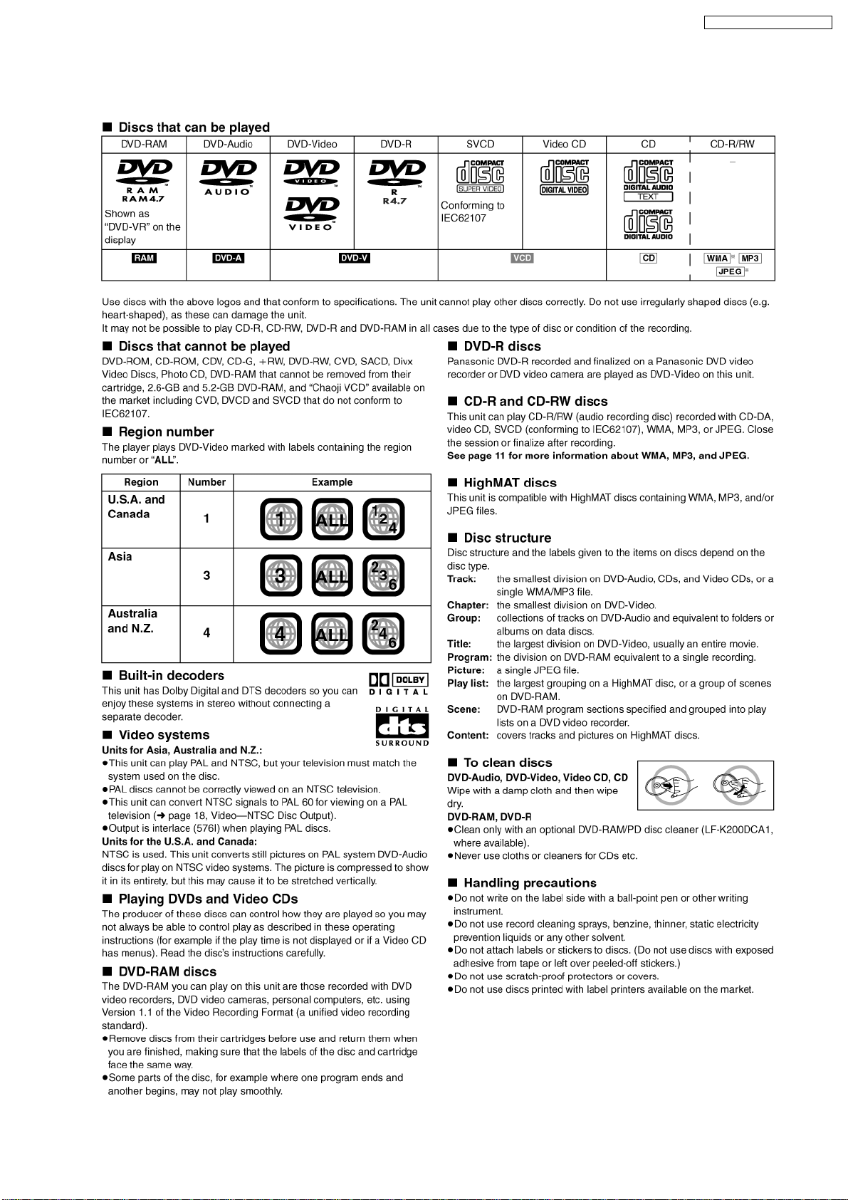
11 Disc information
12 About HighMAT
12.1. What is HighMAT?
12.2. Why use HighMAT?
12.3. The advantages of using HighMAT
12.4. Outline of the HighMAT standard
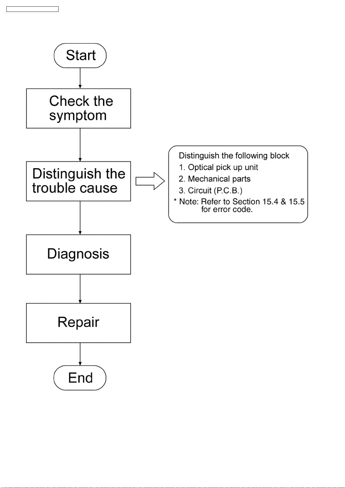
13 Procedure for repairing the set
13.1. Distinguish the trouble cause
2
6
7
8
9
11
13
13
13
13
14
16
17
Page 3

SA-VK61DGC / SA-VK61DGCS
13.2. Diagnosis of Optical Pick-up Unit 19
14 Optical Pickup Self-Diagnosis and Replacement Procedure
14.1. Self-diagnosis
14.2. Cautions to Be Taken During Replacement of Optical
Pickup and Spindle Motor
15 Self-Diagn osis Function
15.1. Automatic Displayed Error Codes
15.2. Memorized Error Codes
15.3. Mode Table 1
15.4. DVD/CD Self-Diagnosis Error Code Description
15.5. Error Codes Stored During No Play
15.6. Mode Table 2
15.7. Tray Lock Function
15.8. Things to Do After Repair
16 Cautions To Be Taken During Servicing
16.1. Recovery after the dvd player is repaired
16.2. DVD Player Firmware Version Upgrade Process
16.3. Firmware Version Upgrade Process by Using Disc and
Recovery Process
16.4. Using Recovery Disc
16.5. Total Usage Time Display
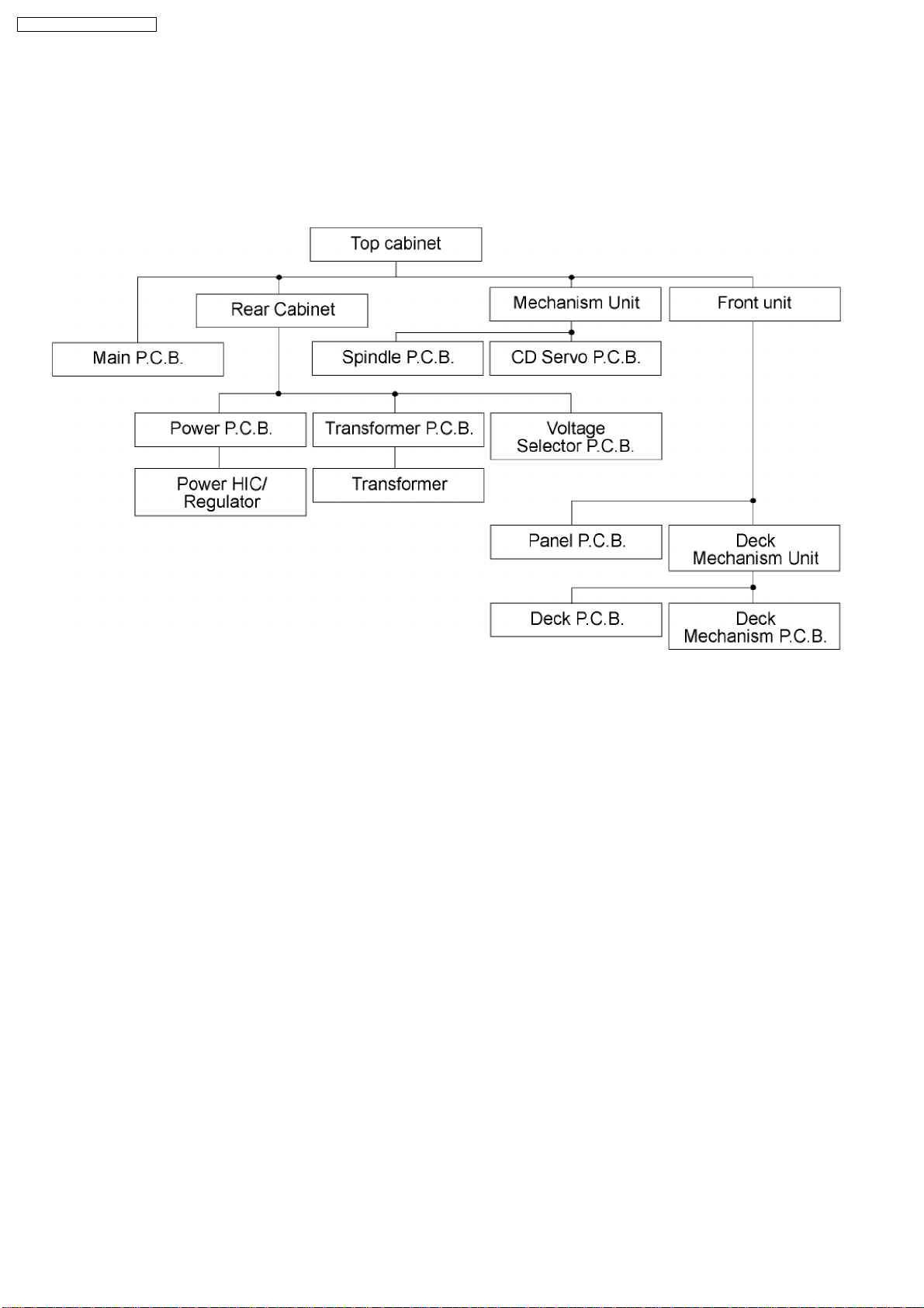
17 Disassemb ly and Assembly of Main Component
17.1. Disassembly flow chart
17.2. Disassembly of Top Cabinet
17.3. Disassembly of DVD Module (2) P.C.B.
17.4. Disassembly for the Top Ornament Unit
17.5. Disassembly for DVD changer unit
17.6. Disassembly for Panel P.C.B., LED P.C.B. & Tact Switch
P.C.B.
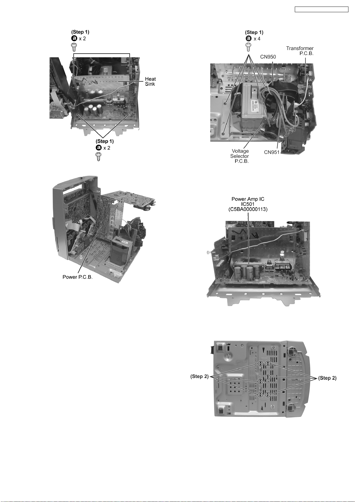
17.7. Disassembly of Main P.C.B., Power P.C.B., Transformer
P.C.B. & Voltage Selector P.C.B.
17.8. DVD Changer Unit Main Component Replacement
Procedures
17.9. Disassembly of Deck Mechanism Unit
17.10. Replacement for the cassette lid ass 馳
17.11. Counter-measure for tape trouble
18 Measurem ents and Adjustments
18.1. Cassette Deck Section
18.2. Tuner Section
18.3. Alignment Points
19 Block Diagram
20 Schematic Diagram
20.1. (A) DVD Module (1) Circuit
21
21
22
23
23
23
23
24
24
24
27
27
28
28
28
28
28
29
30
30
31
31
31
33
33
34
36
49
52
53
54
54
55
56
57
67
20.2. (B) DVD Module (2) Circuit
20.3. (C) Main Circuit & (D) Tuner Extent Circuit
20.4. (E) Panel Circuit, (F) LED Circuit & (G) Tact Switch Circuit
20.5. (H) Tuner Circuit
20.6. (J) Deck Circuit & (K) Deck Mechanism Circuit
20.7. (L) Power Supply Circuit
20.8. (M) Power Circuit
20.9. (N) Transformer Circuit, (O) AC Inlet Circuit, (P) Voltage
Selector Circuit, (Q) CD Loading Circuit, (R) CD Detect
Circuit & (S) Spindle Position Circuit
21 Printed Circuit Board
21.1. (A) DVD Module (1) P.C.B. (Component & Foil Side)
21.2. (B) DVD Module (2) P.C.B. (Side A & B)
21.3. (B) Main P.C.B.
21.4. (D) Tuner Extent P.C.B., (F) LED P.C.B. & (G) Tact P.C.B.
21.5. (E) Panel P.C.B.
21.6. (H) Tuner P.C.B. & (I) Tuner Pack P.C.B.
21.7. (J) Deck P.C.B. & (K) Deck Mechanism P.C.B.
21.8. (L) Power Supply P.C.B.
21.9. (M) Power P.C.B.
21.10. (N) Transformer P.C.B.
21.11. (O) AC Inlet P.C.B. & (P) Voltage Selector P.C.B.
21.12. (Q) CD Loading P.C.B., (R) CD Detect P.C.B. & (S)
Spindle Position P.C.B.
22 Wiring Connection Diagram
23 Illustration of ICs, Transistors and Diodes
24 Terminal Function of IC
24.1. IC600 (C2BBHF000076
) (GC) IC600 (C2BBHF000077) (GCS) System
Microprocessor
25 Parts Location and Replacement Parts List
25.1. Deck Mechanism (RAA3412-S)
25.2. CD Loading Mechanism (RD-DAC036-S)
25.3. Cabinet
25.4. Electrical Parts List
25.5. Packing Materials & Accessories Parts List
25.6. Packaging
68
70
81
93
97
99
101
103
105
106
106
107
111
113
114
116
117
118
120
122
123
124
125
127
128
128
129
130
133
137
140
153
154
1 Before Use
Be sure to disconnect the mains cord before adjusting the voltage selector.
Use a minus(-) screwdriver to set the voltage selector (on the rear panel) to the voltage setting for the area in which the unit will
be used. (If the power supply in your area is 117V or 120V, set to the “127V” position.)
Note that this unit will be seriously damaged if this setting is not made correctly. (There is no voltage selector for some countries,
the correct voltage is already set.)
2 Before Repair and Adjustment
Disconnect AC power, discharge Power Supply Capacitors C531~C534, C588~C589, C598~C599 and C954 through a 10Ω,5W
3
Page 4
SA-VK61DGC / SA-VK61DGCS
resistor to ground.
DO NOT SHORT-CIRCUIT DIRECTLY (with a screwdriver blade, for instance), as this may destroy solid state devices.
After repairs are completed, restore power gradually using a variac, to avoid overcurrent.
Current consumption at AC 110/127/220~230V, 50/60 Hz in NO SIGNAL (vol. min, at CD mode) & AC 240 V, 50 Hz should be
~770mA .
3 Protection Circuitry
The protection circuitry may have operated if either of the following conditions are noticed:
No sound is heard when the power is turned on.
·
Sound stops during a performance.
·
The function of this circuitry is to prevent circuitry damage if, for example, the positive and negative speaker connection wires are
“shorted”, or if speaker systems with an impedance less than the indicated rated impedance of the amplifier are used.
If this occurs, follow the procedure outlines below:
1. Turn off the power.
2. Determine the cause of the problem and correct it.
3. Turn on the power once again after one minute.
Note :
When the protection circuitry functions, the unit will not operate unless the power is first turned off and then on again.
4 Safety Precautions
4.1. General Guidelines
1. When servicing, observe the original lead dress. If a short circuit is found, replace all parts which have been overheated or
damaged by the short circuit.
2. After servicing, see to it that all the protective devices such as insulation barriers, insulation papers shields are properly
installed.
3. After servicing, make the following leakage current checks to prevent the customer from being exposed to shock hazards.
4.1.1. Leakage Current Cold Check
1. Unplug the AC cord and connect a jumper between the two prongs on the plug.
2. Measure the resistance value, with an ohmmeter, between the jumpered AC plug and each exposed metallic cabinet part on
the equipment such as screwheads, connectors, control shafts, etc. When the exposed metallic part has a return path to the
chassis, the reading should be between 1MΩ and 5.2MΩ.
When the exposed metal does not have a return path to the chassis, the reading must be ・.
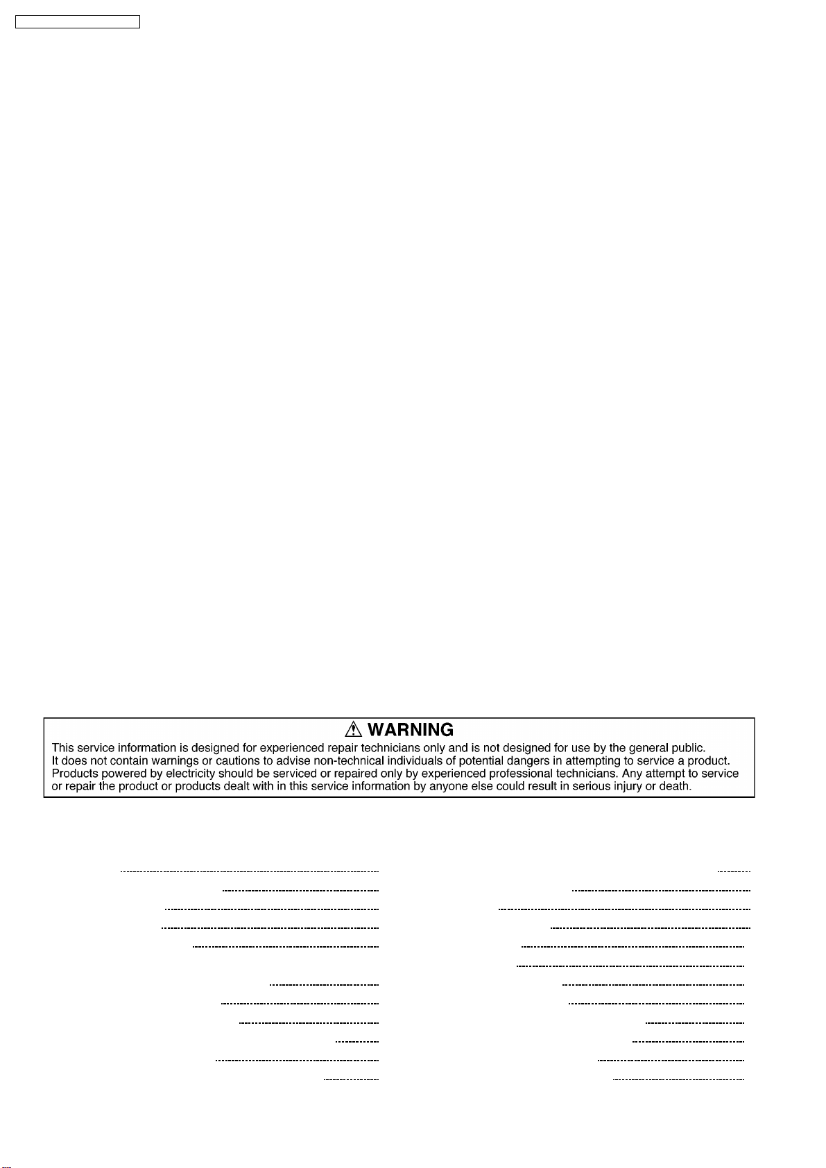
Figure 1
4.1.2. Leakage Current Hot Check
(See Figure 1)
1. Plug the AC cord directly into the AC outlet. Do not use an isolation transformer for this check.
2. Connect a 1.5kΩ, 10 watts resistor, in parallel with a 0.15µF capacitor, between each exposed metallic part on the set and a
good earth ground such as a water pipe, as shown in Figure 1.
3. Use an AC voltmeter, with 1000 ohms/volt or more sensitivity, to measure the potential across the resistor.
4. Check each exposed metallic part, and measure the voltage at each point.
5. Reverse the AC plug in the AC outlet and repeat each of the above measurements.
4
Page 5

SA-VK61DGC / SA-VK61DGCS
6. The potential at any point should not exceed 0.75 volts RMS. A leakage current tester (Simpson Model 229 or equivalent) may
be used to make the hot checks, leakage current must not exceed 1/2 milliamp. In case a measurement is out of the limits
specified, there is a possibility of a shock hazard, and the equipment should be repaired and rechecked before it is returned to
the customer.
5 Prevention of Electro Static Discharge (ESD) to
Electrostatically Sensitive (ES) Devices
Some semiconductor (solid state) devices can be damaged easily by electricity. Such components commonly are called
Electrostatically Sensitive (ES) Devices. Examples of typical ES devices are integrated circuits and some field-effect transistors and
semiconductor “chip” components. The following techniques should be used to help reduce the incidence of component damage
caused by electro static discharge (ESD).
1. Immediately before handling any semiconductor component or semiconductor-equiped assembly, drain off any ESD on your
body by touching a known earth ground. Alternatively, obtain and wear a commercially available discharging ESD wrist strap,
which should be removed for potential shock reasons prior to applying power to the unit under test.
2. After removing an electrical assembly equiped with ES devices, place the assembly on a conductive surface such as aluminium
foil, to prevent electrostatic charge build up or exposure of the assembly.
3. Use only a grounded-tip soldering iron to solder or unsolder ES devices.
4. Use only an anti-static solder remover device. Some solder removal devices not classified as “anti-static (ESD protected)” can
generate electrical charge to damage ES devices.
5. Do not use freon-propelled chemicals. These can generate electrical charges sufficient to damage ES devices.
6. Do not remove a replacement ES device from its protective package until immediately before you are ready to install it. (Most
replacement ES devices are packaged with leads electrically shorted together by conductive foam, aluminium foil or
comparable conductive material).
7. Immediately before removing the protective material from the leads of a replacement ES device, touch the protective material
to the chassis or circuit assembly into which the device will be installed.
Caution
Be sure no power is applied to the chassis or circuit, and observe all other safety precautions.
8. Minimize body motions when handling unpackaged replacement ES devices. (Otherwise harmless motion such as the brushing
together of your clothes fabric or the lifting of your foot from a carpeted floor can generate static electricity (ESD) sufficient to
damage an ES device).
6 Handling the Lead-free Solder
6.1. About lead free solder (PbF)
Distinction of PbF P.C.B.:
P.C.B.s (manufactured) using lead free solder will have a PbF stamp on the P.C.B.
Caution:
· Pb free solder has a higher melting point than standard solder; Typically the melting point is 50 - 70°F (30 - 40°C) higher. Please
use a high temperature soldering iron. In case of soldering iron with temperature control, please set it to 700 ± 20°F (370 ±
10°C).
· Pb free solder will tend to splash when heated too high (about 1100°F/600°C).
· When soldering or unsoldering, please completely remove all of the solder on the pins or solder area, and be sure to heat the
soldering points with the Pb free solder until it melts enough.
5
Page 6
SA-VK61DGC / SA-VK61DGCS
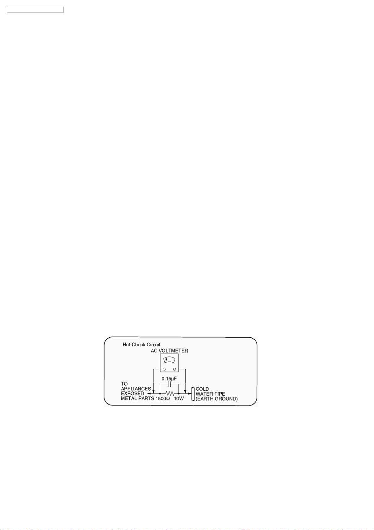
7 Cautions to be taken when handling Optical Pickup
The laser diode used inside optical pickup could be destroyed due to static electricity as a potential difference is caused by
electrostatic load discharged from clothes or human body. Handling the parts carefully to avoid electrostatic destruction during
repair.
7.1. Handling Optical Pickup
1. Do not impact on optical pickup as the unit structurally uses an extremely precise technology.
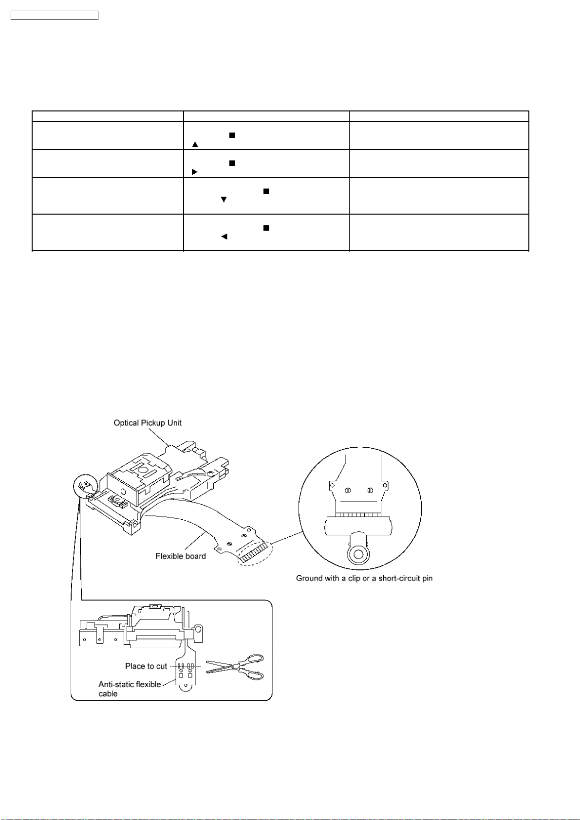
2. Short-circuit the flexible cable of optical pickup remove from the circuit board using a short-circuit pin or clip in order to prevent
laser diode from electrostatic destruction (Refer to Fig. 7.1 and Fig. 7.2)
3. Do not handle flexible cables forcibly as this may cause snapping. Handle the parts carefully (Refer to Fig. 7.1)
4. A new optical pickup is equipped with an anti-static flexible cable. After replacing and connecting to the flexible board, cut the
anti-static flexible cable. (Refer to Fig. 7.1)
Fig. 7.1
7.2. Replacing Precautions for Optical Pickup Unit
DVD/CD Optical Pickup
The optical pickup by which part supply was carried out attaches the short clip to the flexible board for laser diode electrostatic
discharge damage prevention. Please remove the short clip and be sure to check that the short land is open, before connecting.
(Please remove solder, when the short land short-circuits.)
7.3. Grounding for Preventing Electrostatic Destruction
1. Human body grounding
Use the anti-static wrist strap to discharge the static electricity accumulated in your body. (Refer to Fig. 7.2)
2. Work place grounding
Place a conductive material (conductive sheet) or ironboard where optical pickup is placed. (Refer to Fig. 7.2)
Note :
Keep your clothes away from optical pickup as wrist strap does not release the static electricity charged in clothes.
Fig. 7.2
6
Page 7
SA-VK61DGC / SA-VK61DGCS
8 Precaution of Laser Diode
Caution :
This product utilizes a laser diode with the unit turned "ON", invisible laser radiation is emitted from the pick up lens.
Wavelength : 780 nm(CD)/658 nm(DVD)
Maximum output radiation power from pick up : 100 µW/VDE
Laser radiation from pick up unit is safety level, but be sure the followings:
1. Do not disassemble the optical pick up unit, since radiation from exposed laser diode is dangerous.
2. Do not adjust the variable resistor on the pick up unit. It was already adjusted.
3. Do not look at the focus lens using optical instruments.
4. Recommend not to look at pick up lens for a long time.
CAUTION!
THIS PRODUCT UTILIZES A LASER.
USE OF CONTROLS OR ADJUSTMENTS OR PERFORMANCE OF PROCEDURES OTHER THAN THOSE SPECIFIED HEREIN MAY RESULT
IN HAZARDOUS RADIATION EXPOSURE.
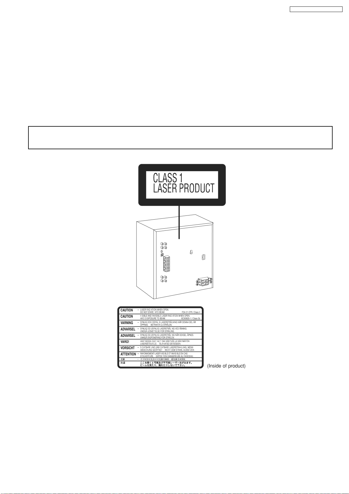
n Use of Caution Labels
7
Page 8
SA-VK61DGC / SA-VK61DGCS
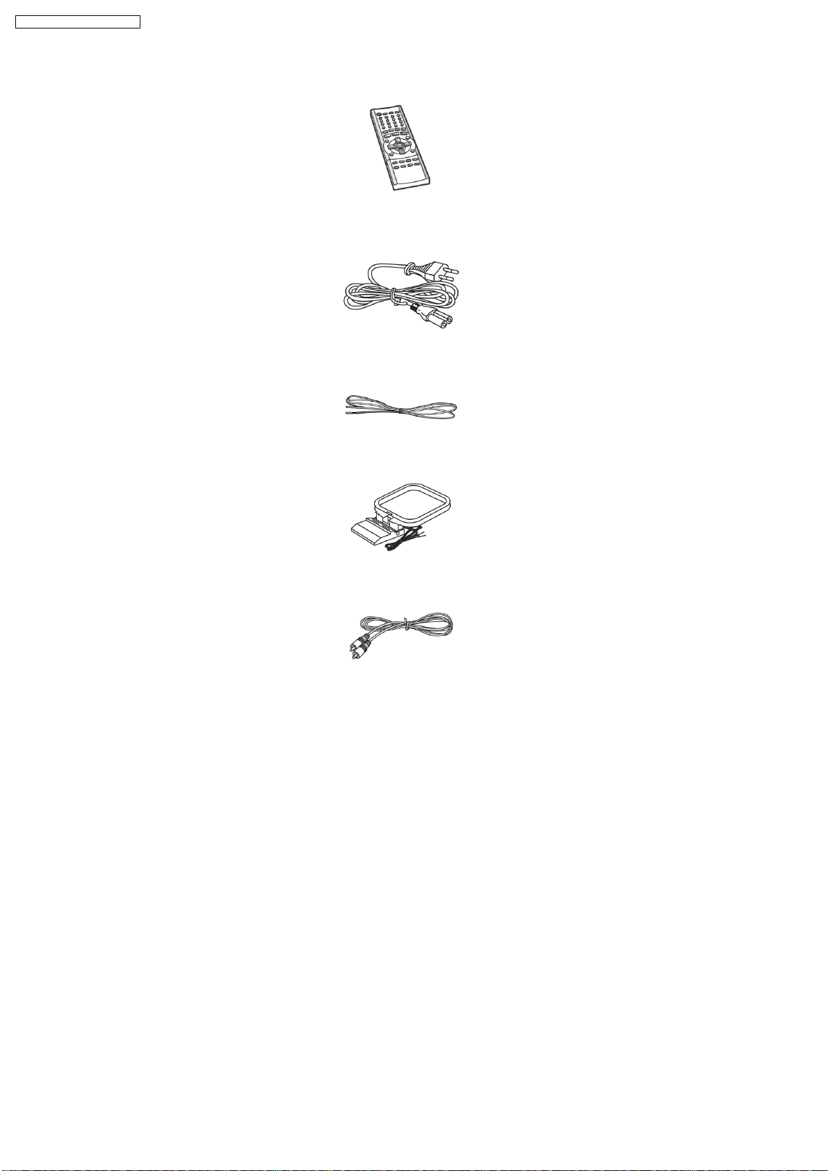
9 Accessories
Remote
control
AC power supply cord
FM indoor antenna
AM indoor antenna
Video cable
8
Page 9
10 Operation Procedures
SA-VK61DGC / SA-VK61DGCS
9
Page 10
SA-VK61DGC / SA-VK61DGCS
10
Page 11
11 Disc information
SA-VK61DGC / SA-VK61DGCS
11
Page 12
SA-VK61DGC / SA-VK61DGCS
12
Page 13
SA-VK61DGC / SA-VK61DGCS
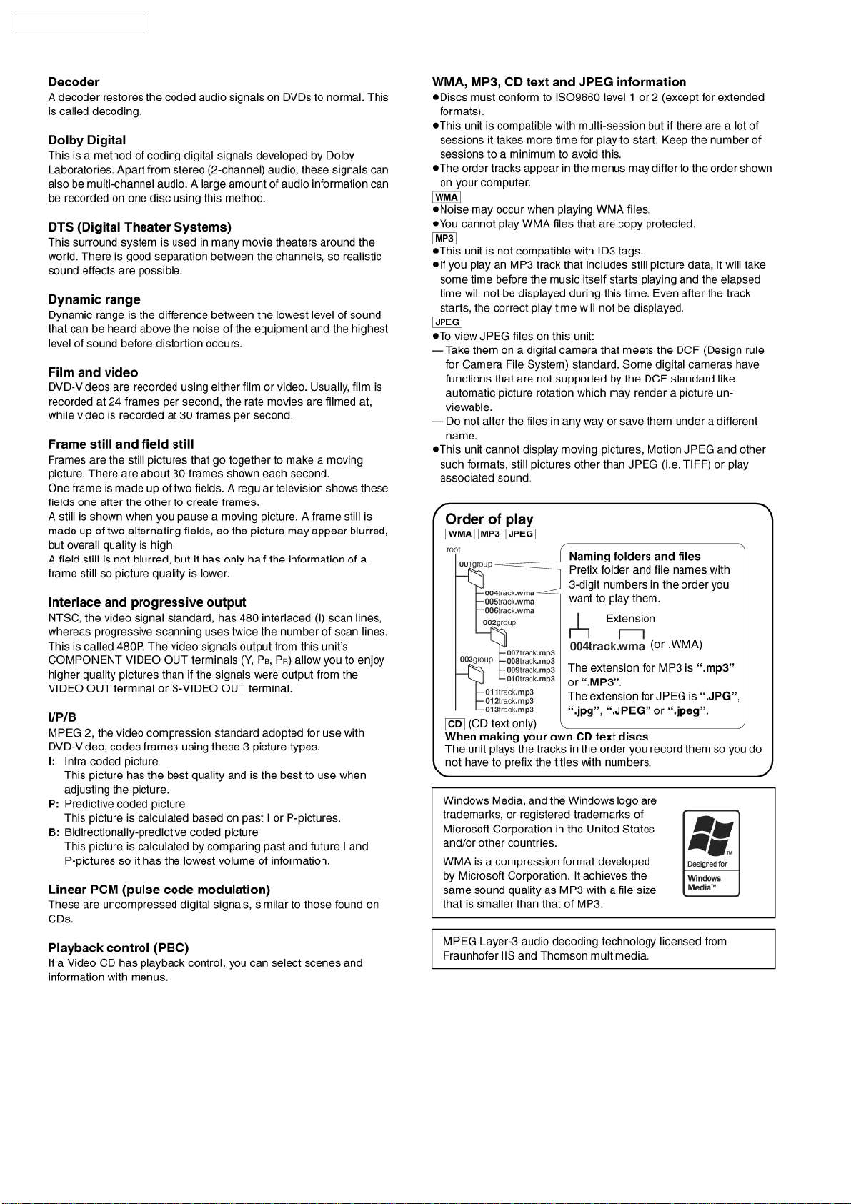
12 About HighMAT
12.1. What is HighMAT?
This word combines the abbreviations of Matsushita Electric Industrial Co. Ltd. and High Performance Media Access Technology,
and is a trademark of Microsoft Corporation. The products with the HighMAT logo shown below are made according to the
HighMAT standard.
HighMAT is a format that allows users to save digital contents such as photographs, audio, and images on a CD. This gives
consistency in the way of reading data when general consumer products (such as DVD players) and PCs are used, and thus, it is
easy to operate for the user.
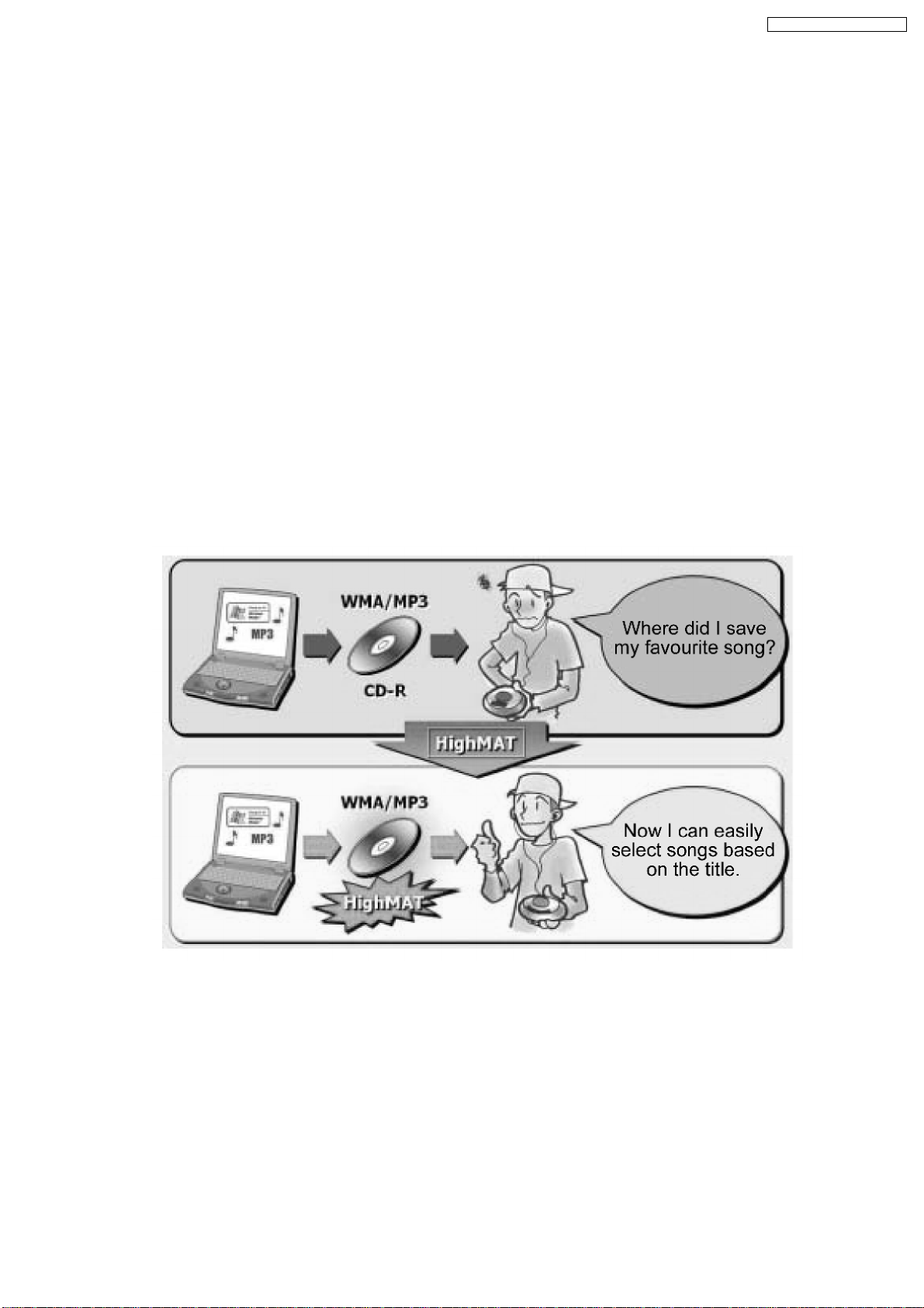
12.2. Why use HighMAT?
Up to now, there was no harmonized standard from playing digital content stored in CD-ROM formats (including CD-R) on
consumer products like DVD players.Therefore, we used to have problems such as follow:
· There was no common play list or attached information on contents, which is called metadata.
· The data compression method differed according to the equipment.
· As the number of CD-ROMs recorded increased retrieved the contents became more difficult.
· Because display and operation methods were different depending on the equipment, the play order of the content on the same
disc could change.
12.3. The advantages of using HighMAT
Applying the HighMAT standard will solve the following problems and will improve usability.
· It will create a common user interface for both PC and consumer products.
· Regardless of the types of consumer products, such as DVD players, portable CD players, car stereos, and micro computers,
a consistent way to pay for digital content will be created and it will make it easier to retrieve data.
13
Page 14
SA-VK61DGC / SA-VK61DGCS
· You can also play digital content on the disc, which was created in accordance with the HighMAT format with a conventional
CD-ROM player.
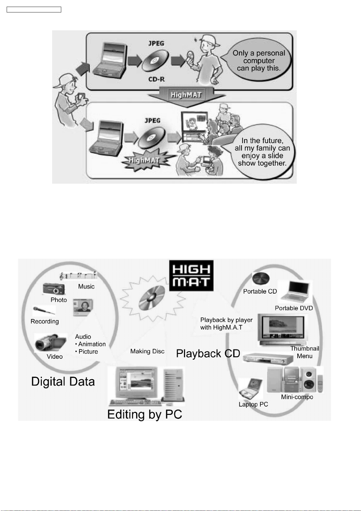
12.4. Outline of the HighMAT standard
1. Recording medium
· CD-R/CD-RW
· Supports ISO 9660 Level Expanded Joliet
· For multiple session
2. Support data format
· Level 1 player: WMA, MP3 (MPEG-1 Audio Layer 3)
· Level 2 player: WMA, MP3 (MPEG-1 Audio Layer 3), JPEG
· Level 3 player: WMA, MP3 (MPEG-1 Audio Layer 3), JPEG, WMV, MPEG4 (optional)
3. Limitation of data format
14
Page 15

SA-VK61DGC / SA-VK61DGCS
· WMA, MP3 (MPEG-1 Audio Layer 3) 64 kbps - 160.999 kbps, 44.1 KHz, stereo, fixed bit rate/ variable bit rate.
· WMA, V2 and above, excluding Lossless/Voice/Pro
· JPEG: Max 6M pixel, Maximum file size: 3 MB
4. Limitations regarding the number of files on the media, etc.
· Total number of audio files: Maximum 450
· Total number of still picture files: Maximum 999
· Total number of animation files: Maximum 200
· Total number of directories: Maximum 400
· Length of a file name: Maximum 108 characters (Unicode)
· Total number of play lists: Maximum 200
· Number of contents in the playlist: Maximum 900
5. Composition of HighMAT disc
· Menu: Classified for the navigation of the HighMAT digital contents. When menu selected, its submenu or the play list will
be displayed.
· Play list: A list in which one or more digital contents are arranged in order
· Group: Sub-divided group of a play list.
· Digital Contents: Audio, still picture, and animation data.
15
Page 16
SA-VK61DGC / SA-VK61DGCS
13 Procedure for repairing the set
16
Page 17
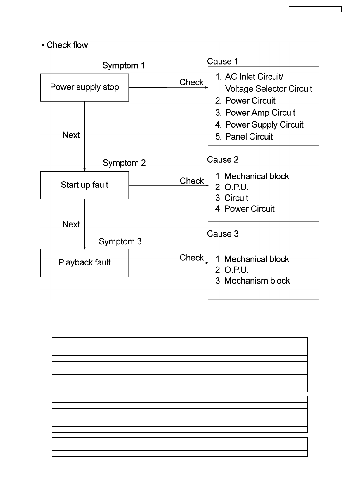
13.1. Distinguish the trouble cause
SA-VK61DGC / SA-VK61DGCS
How to distinguish the trouble
1. View mechanical part if visual damage occurred.
Confirm the movement of mechanical parts assembly
(tray ass’y, loading mechanism ass’y, etc.).
Cause 1 Possible fault
1. AC Inlet Circuit/Voltage Selector Circuit Fuse Blow (F1,F2), Power Transformer Problem(T501,
2. Power Circuit Fuse Blow (F3, F4) FP951, FP950 open
3. Power Amp Circuit IC502 faulty
4. Power Supply Circuit IC500, IC501 faulty
5. Panel Circuit FL Display Problem (-VP → Q950 faulty/ FP951 open/ D961
Cause 2 Possible fault
1. Mechanical block Tray and loading mechanical block, traverse unit, deck unit
2. O.P.U. Refer to the diagnosis of OPU
3. Circuit IC307 faulty (check for pin 31, 32)
4. Power circuit Refer to Cause 1
Cause 3 Possible fault
1. Mechanical block Traverse block (Tilt adjustment)
2. O.P.U. Refer to the diagnosis of OPU
2. Diagnose if Optical Pickup Unit is faulty (refer to
diagnosis of Optical Pickup Unit).
3. If mechanism and OPU are OK, it is P.C.B.
T502), Wrong Selection of Selector (S501)
faulty)
SVS6V to Micro-P (Q951/ D965 faulty) Problem
IC701 faulty (check for pin 2, 23)
17
Page 18

SA-VK61DGC / SA-VK61DGCS
3. DVD Module (1) Circuit IC2501 (Tracking - pin 11 & 12)
4. Main Circuit IC50 faulty (pin 17, 19, 21, 22, 24, 25 & 32 to JK302/JK301)
Cause 3 Possible fault
IC2501 (Focus - pin 13 & 14)
IC2501 (spindle motor - pin 17, 18)
IC2501 ( Traverse motor - pin 15, 16)
FG unit (pin 1, 2 at FP5102)
IC3001, Video Problem (pin 158 (Y/PY/G), pin 160
(CB/PB/B), pin 161 (CR/PR/R), pin 163 (Y) and pin 164 (C))
JK301 & JK302 faulty
IC700 (DSP IC) faulty (ckeck for pin 65, 69, 11, 14)
18
Page 19
13.2. Diagnosis of Optical Pick-up Unit
SA-VK61DGC / SA-VK61DGCS
How to distinguish Laser destruction/damage
Confirmation 1
Remove cover of mechanism block so that you will see the lens of optical pickup.
Confirm emission of laser at the moment when power switch is turned on.
If there is no laser emission, laser diode is faulty.
Confirmation 2
19
Page 20

SA-VK61DGC / SA-VK61DGCS
While pressing & hold “Stop” button on main unit, press “Display” button on the remote controller. Unit display laser current on
FL.
From the reading of display, you can judge if laser diode is damaged or not.
Reading on the right side should be less than 70. If reading is more than 70, laser is damaged.
How to confirm if Optical Pickup is OK
Confirmation 1
1. Confirmation of jitter value with test disc. (Refer below for how to check jitter)
2. Lens cleaning.
3. Reconfirm jitter value.
4. Perform tile adjustment. (Refer to tilt adjustment)
5. Reconfirm jitter value. (To confirm jittervalue, while pressing & hold “Stop” button on main unit, press numeric “5” on remote
controller.)
Unit display jitter value on FL.
Confirmation 2
If servo is very unstable due to optical error and you cannot confirm jitter value, clean the lens and check appearance of pick
up unit (cutting coil of actuator, etc), then check circuitry.
20
Page 21
SA-VK61DGC / SA-VK61DGCS
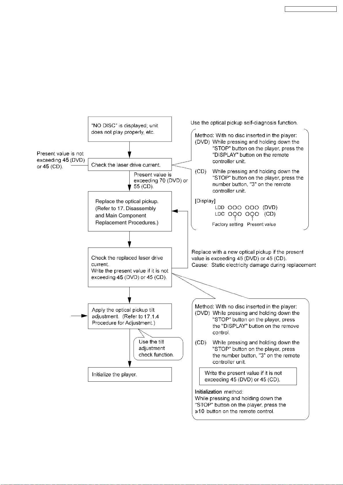
14 Optical Pickup Self-Diagn osis and Replacem ent
Procedure
14.1. Self-diagnosis
This unit is equipped with the optical pickup self-diagnosis function and the tilt adjustment check function. Follow the procedure
described below during repair in order to perform self-diagnosis and tilt adjustment effectively. Especially when “NO DISC” is
displayed, be sure to apply the self-diagnosis function before replacing with an optical pickup. Replacement of optical pickup
generally requires when the present value of laser drive exceeds 45 (DVD) or 45 (CD).
Note:
Start diagnosis within three minutes after turning on the power (as diagnosis fails when the unit becomes warm).
21
Page 22
SA-VK61DGC / SA-VK61DGCS
14.2. Cautions to Be Taken During Replacement of Optical Pickup and
Spindle Motor
Before replacing the optical pickup and spindle motor, check a total usage time respectively. Follow the checking method described
below.
Item Status and Key Function Display
Checking DVD, CD laser usage time With the unit stopped and no disc inserted,
press the.
button on the remote controller unit.
Checking spindle motor usage time With the unit stopped and no disc inserted,
press the
button on the remote controller unit.
Resetting DVD, CD laser usage time While the DVD and CD laser usage times are
displayed, press the
and the
unit.
Resetting spindle motor usage time While the spindle motor usage time is
displayed, press the
and the
unit.
button on the player and the
button on the player and the
button on the player
button on the remote controller
button on the player
button on the remote controller
14.2.1. Cautions to be taken during replacement of optical pickup
Optical pickup could be damaged due to the static electricity discharged from human body. Wear proper protection gear against
static electricity during optical pickup and its peripheral repair. (Refer to “Cautions to Be Taken When Handling Optical Pickup”.)
· Do not touch laser diode, actuator and their peripherals.
· Do not check laser diode with a tester and such. (The tester will be destroyed.)
· For short-circuiting or removing laser diode, the use of an anti-static soldering iron is recommended. (Recommended model:
HAKKO ESD product)
· Solder the land of the flexible cable in the optical pickup.
Note:
If an anti-static soldering iron is not available, short-circuit the terminal surface of the flexible cable and then the land using a
clip or equivalent device.
T1_xxxx_yyyy
xxxx(DVD), yyyy(CD): total time is displayed with a
four-digit number by the ten hours.
T2_xxxxx
xxxxx: total time is displayed with a four-digit
number by the ten hours.
T1_0000_0000
T2_0000
22
Page 23

SA-VK61DGC / SA-VK61DGCS
15 Self-Diagnosis Function
This unit is equipped with the self-diagnosis function, which displays an error when it occurs, for use during servicing.
15.1. Automatic Displayed Error Codes
15.1.1. Automatic Display Function
For a power unit error, the code is automatically displayed.
F61: Automatically displayed on the LCD of the player.
15.1.2. Re-Display
· For F61 Display
−
− When the code, F61 is displayed, the power is automatically turned off.
− −
−
− The code, F61 is displayed for three seconds, and then the current time appears.
− −
−
− To retrieve the code, turn on the power button so that the code F61 appears, however, is switched to time display after three
− −
seconds, and the power is automatically turned off.
· For F76 Display
−
− The abnormalities is an output or the abnormalities in a power supply of POWER AMP.
− −
15.1.3. Description of Error Code
15.1.3.1. F61
· State, Condition
When the power is turned on, the unit is automatically turned off. The power does not turn on.
· Cause, Troubleshooting
Power circuit system failure and/or direct current flown to speaker terminal
Identify the cause and replace with new parts.
15.2. Memorized Error Codes
15.2.1. Activating Self-Diagnosis Function and Displaying Method
1. Turn on the power.
2. Select DVD/CD function. With no DVD/CD inserted in the player, press and hold down the
and press the “0” button on the remote control for at least two seconds in order to display “DVD_F_ _ _ ”.
3. Press the
If several errors are detected, press the
button. If a memorized error is detected, the result of self diagnosis is displayed. (Ex.: T H15)
button to display each.
button for at least two seconds,
15.2.2. Re-Display
· Press the power button to turn off the power, and then turn on the power.
· The details of self diagnosis are stored in the unit memo ry.
To retrieve them, follow the procedure described the above, “Activating Self-Diagnosis Function and Displaying Method”.
15.3. Mode Table 1
Following modes are available with combinations of the pressed buttons on the player and on the remote controller unit.
Player Remote Controller Unit Usage
button
0 Error code display (Refer to the Item 15.4. DVD Error Code Description)
5 Tilt adjustment (Jitter)
6 Region number and broadcasting system check
8 Bulit-in program version check (Micro-P)
DISPLAY DVD laser drive current check
3 CD laser drive current check
PAUSE Writing of laser drive current value after replacement of optical pickup
(Do use this function only when optical pickup is replaced.)
Initialization of the player (factory setting is restored.)
Used after replacement of micro-computer and its peripherals and printed circuit board.
23
Page 24
SA-VK61DGC / SA-VK61DGCS
15.4. DVD/CD Self-Diagnosis Error Code Description
Error Code State, Conditon Cause, Troubleshooting
H15 The disc tray cannot be opened: it closes spontaneously. Disc tray open/close detection switch (S1001) failure.
H16 The disc tray cannot be closed: it opens spontaneously.
Error Code Meaning Details
U. H. Error
U11 Focus servo failure
H01 Tray loading failure
H02 Spindle servo failure (Spindle servo, DSC, SP motor, CLV servo failure)
H03 Traverse motor failure
H04 Tracking servo error
H05 Seek timeout failure
DSC system
F500 DSC failure DSC stops due to servo failure.
F501 DSC not Ready failure Communication failure between DSC and system computer
F502 DSC Time out failure See F500.
F503 DSC communication failure Communication failure (Result failure occurs after communication
F505 DSC Attention Error See F500.
F506 Invalid media Disc is placed upside down; TOC is unreadable or invalid disc is
Disc Code
F103 Ilegal highlight position Disc standard is possibly illegal when highlight is displayed.
IIC Error
F4FF Forced initialization failure (Time out)
F880 Unsuitable task number When a message arrives from not existing task
F890 A message is sent during AV task transmission During transmission of a message to AV task
F891 Unable to transmit a message to AV task When transmission of a message to AV task starts
F893 FROM altered
F894 EEPROM failure
F895 Firmware version compatibility problem
F897 Incomplete initialization
F8A0 Unsuitable message command When transmission of a message to AV task starts
(Check and replace)
(Startup, focus failure, etc.)
(No communication because DSC does not move)
command is transmitted.)
inserted.
15.5. Error Codes Stored During No Play
Error Code Meaning System Computer Item Setting Task Internal error in system
F0BF 6) Unable to replay due to physical layer
identification failure
F0C0 8) DVD: Unable to replay due to no DVD
Video/Audio/VR
F0C1 9) DVD: Prohibited due to illegal regional
code
F0C2 A) DVD: No replay due to PAL system PCND_NOPLAY_PAL 0x90 DiscManager 0xD0C2
F0C3 B) DVD: All title replay prohibited in parental
setting
F0C4 C) VCD: Prohibited due to PHOTO CD
format
F0C5 D) VCD/CD: Prohibited due to CD-ROM
without CD-DA
PCND_NOPLAY_PHYSICAL 0x50 DriveManager 0xD0BF
PCND_NOPLAY_VIDEO 0x70 DiscManager 0xD0C0
PCND_NOPLAY_RCD 0x80 DiscManager 0xD0C1
PCND_NOPLAY_PTL 0xA0 DiscManager 0xD0C3
PCND_NOPLAY_PHOTOCD 0xB0 DiscManager 0xD0C4
PCND_NOPLAY_CDROM 0xC0 DiscManager 0xD0C5
computer
15.6. Mode Table 2
Following modes are available with combinations of the pressed buttons on the player and on the remote controller unit.
24
Page 25
SA-VK61DGC / SA-VK61DGCS
Item Operational
Condition and Key
Function
Jitter display While the player is
stopped and no disc is
inserted, press and
hold down the
button on the player
and the number
button, “5” on the
remote controller unit.
Error code display While the player is
stopped and no disc is
inserted, press and
hold down the
button on the player
and the number
button, “0” on the
remote controller unit.
Measurement of laser
current electricity
initialization value
While the player is
stopped and no disc is
inserted, press and
hold down the
button on the player
and the
button
on the remote
controller unit.
Details Display TO Exit Mode
Jitter display
Measures and displays jitter.
Measurement is repeated every
second. Read error counter starts at 0
at the mode setting, and increased by
one as data read fails at target block. A
small defect is allowed to correct by
retry. Any possibility is counted as one
increment. Repetitive errors after retry
increase by two levels or more.
Error code display
Displays the latest error code stored in
EEPROM.
Measurement of laser current
electricity initialization value
Memorizes each initialization value of
DVD and CD in EEPROM.
J*1xxx*2_yyy*3_zz
*1
: Jitter display mode
*2
: Jitter measurement value
*3
: Read error counter
*4
: Focus driving value
*4
Values are shown to one decimal
place in the decimal digit.Focus
driving value is displayed in the
hexadecimal digit.
DVDnn_F---
*nn: Error history
*--: Error number
DVD 01 FOBF
LDO*1_013*2_032
*1
: Laser current electricity
measurement mode
*2
: DVD current electricity value
*3
: CD current electricity value
*3
Press the STOP or
OPEN button.
Press the OPEN
button.
Automatically exits
the mode after five
seconds.
Measurement of DVD
laser current electricity
ADSC internal RAM
display
While the player is
stopped and no disc is
inserted, press and
hold down the
button on the player
and the DISPLAY
button on the remote
controller unit.
While the player is
stopped and no disc is
inserted, press and
hold down the
button on the player
and the number button
“1” or “2” on the remote
controller unit.
Measurement of DVD laser current
electricity
Measures DVD laser current electricity
and displays the result together with
the initialization value stored in
EEPROM. After measurement, DVD
laser is lit till the power is turned off (or
goes off when the primary power is
turned off).
ADSC internal RAM display
Reads and displays the RAM value
inside ADSC. The address is renewed
when the CLEAR key is pressed so
that the values at eleven points appear.
Values are shown in the decimal
digit. The above example indicates
that the current electricity
initialization value is 13mA at DVD
laser and 32mA at CD laser when
laser is turned on.
LDD*1_012*2_014
*1
: DVD laser current electricity
measurement mode
*2
: Current electricity initialization
value stored in EEPROM
*3
: Present value of current
*3
electricity
Values are shown in the decimal
digit. The above example indicates
that the current electricity
initialization value is 12mA and its
present value is 14mA.
A*1_FB0*2_0000
*1
:ADSC internal RAM display
mode
*2
: Address
*3
: RAM value at displayed
*3
address
Automatically exits
the mode after five
seconds.
Press the STOP or
OPEN button.
25
Values are shown in the
hexadecimal digit. The above
example indicates that ADSC
value at the address, FB0h is
0000h.
Page 26
SA-VK61DGC / SA-VK61DGCS
Item Operational
Condition and Key
Function
Measurement of CD
laser current electricity
While the player is
stopped and no disc is
inserted, press and
hold down the
button on the player
and the number button
“3” on the remote
controller unit.
User initialization While the player is
stopped and no disc is
inserted, press and
hold down the
button on the player
and the number button
on the remote
controller unit.
Region display While the player is
stopped and no disc is
inserted, press and
hold down the
button on the player
and the number
button, “6” on the
remote controller unit.
Firmware version
display
While the player is
stopped and no disc is
inserted, press and
hold down the
button on the player
and the number
button, “7” on the
remote controller unit.
Region and firmware
display
While the player is
stopped and no disc is
inserted, press and
hold down the
button on the player
and the number
button, “8” on the
remote controller unit.
Laser use time While the player is
stopped and no disc is
inserted, press and
hold down the
button on the player
and the
button
on the remote
controller unit.
Reset laser use time While the usage time 1
is displayed, press and
hold down the
button on the player
and the
button
on the remote
controller unit.
Spindle use time While the player is
stopped and no disc is
inserted, press and
hold down the
button on the player
and the
button
on the remote
controller unit.
Details Display TO Exit Mode
Measurement of CD laser current
electricity
Measures CD laser current electricity
and displays the result together with
the initialization value stored in
EEPROM. After measurement, CD
laser is lit till the power is turned off (or
goes off when the primary power is
LDC*1_032*2_032
*1
: CD laser current electricity
measurement mode
*2
: Current electricity initialization
value stored in EEPROM
*3
: Present value of current
electricity
turned off).
Values are shown in the decimal
digit. The above example indicates
the current electricity initialization
value is 28mA and its present
value is 26mA when laser is turned
on.
User initialization
“INITIALIZE” The user setting recovers the factory
setting.
Region display [srrrxxyzzzz]
s : Panecon model type
rrr : Panecon release number
x : Syscon generation (45)
y: Syscon model type
zzz: Syscon release number
Firmware version display rrr*1_xx*2y*3zzz
*1
: Panel computer release number
*2
: System computer generation
*3
: System computer model type
*4
: System computer release
number
Region and firmware version display _r*1__xx*2y*3zzz
*1
: Region number
*2
: System computer generation
*3
: System computer model type
*4
: System computer release
number
Laser usage time
T1_1234_5678
Measures each for DVD and CD
respectively.
The numbers in the left show
usage time for DVD laser and
those in the right for CD laser. The
four-digit number is shown by the
ten hours in the decimal digit. The
number after 0000 is 9999.
Laser usage time reset
T1_0000_0000 Automatically exits
Resets both for DVD and CD at once.
Spindle motor usage time T2_12345
The four-digit number is shown by
the ten hours in the decimal digit.
The number after 00000 is 99999.
*3
Automatically exits
the mode after five
seconds.
Automatically exits
the mode after five
seconds.
*4
Automatically exits
the mode after five
seconds.
*4
Automatically exits
the mode after five
seconds.
Automatically exits
the mode after five
seconds.
the mode after five
seconds.
Automatically exits
the mode after five
seconds.
26
Page 27
SA-VK61DGC / SA-VK61DGCS
Item Operational
Reset spindle use
time
Communication error
display
Condition and Key
Function
While the usage time 2
is displayed, press and
hold down the
button on the player
and the
on the remote
controller unit.
While the player is
stopped and no disc is
inserted, press and
hold down the
button on the player
and the MENU button
on the remote
controller unit.
button
Usage time 2 reset
Spindle motor usage time
Displays frequency of communication
errors between system computer firm
IC and mechanical computer IC during
DVD module.
Details Display TO Exit Mode
T2_00000 Automatically exits
the mode after five
seconds.
ERR_00/30 Automatically exits
the mode after five
seconds.
15.7. Tray Lock Function
15.7.1. Setting
· Disc Lock Function
1. With the SELECTOR on DVD/CD and POWER ON, hold down the [
[POWER] KEY on the remote control for 3 seconds to enter to Lock mode A.[_ _ _LOCKED_] will be displayed for 3
seconds, and then current disc will begin playing.
2. In Lock mode A, the following key is disabled.
[OPEN/CLOSE]
· Operation Lock Function
1. With the SELECTOR on DVD/CD and POWE R ON, hold down the [CD PLAY] KEY on the main unit, and then press the
[POWER] KEY on the remote control for 3 seconds to enter Lock mode B.
[_ _ _ LOCKED_] will be displayed for 3 seconds, and the current disc will begin playing.
2. Lock mode B primarily controls the selector and disc operations, and disenables for the following keys.
Note:
OPEN/CLOSE
· Prohibiting operation of selector and disk
button are invalid and the player displays “___LOCKED_” while the lock function mode is entered.
1. Select the DVD/CD function.
2. Press and hold down the
button on the player and the power button on the remote controller unit for at least three
seconds. (The message, “___LOCKED_” appears when the function is activated.)
Note:
The following buttons are invalid and the player displays “___LOCKED_” while the lock function mode is entered.
STOP] KEY on the main unit, and then press the
15.8. Things to Do After Repair
Follow the procedure described below after repair.
1. While the power is on, press the
2. Press the power button to turn off the power.
3. Unplug the power cable.
Note:
It is prohibited to unplug the power cable while the tray is opened and to close the tray manually.
button to close the tray.
27
Page 28

SA-VK61DGC / SA-VK61DGCS
16 Cautions To Be Taken During Servicing
16.1. Recovery after the dvd player is repaired
· When Flash ROM or module(2) P.C.B. is replaced, carry out the recovery processing to optimize the drive. Playback the
recovery disc to process the recovery automatically.
· Recovery disc (Product number=RFKZD03R004)
· Performing recovery
1. Load the recovery disc (Product number: RFKZD03R004) to the player and run it.
2. Recovery is performed automatically. When it is finished, a message appears on the screen.
3. Remove the recovery disc.
4. Turn off the power.
Note:
This unit requires no initialization process carried out after the traditional DVD players were repaired. When the recovery
measures are taken, the customer setting will return to the factory setting as same as the procedure described in item
“Initialization” in 9.6 is carried out. Write down the contents of the setting before recovery processing, and reset the player.
16.2. DVD Player Firmware Version Upgrade Process
Firmware of DVD player may upgrade to conform to improvement of its performance and quality including operational range,
playability of non-standardized discs, etc. The version upgrade disc contains the recovery function, and the recovery disc is not
necessary.
Note:
Version upgrade process cannot be complete if the AC power is cut off due to power failure and other occasions during the
process. If this occurs, replace FLASH ROM and restart version upgrade. Version upgrade disc number is informed when
ordered.
16.3. Firmware Version Upgrade Process by Using Disc and Recovery
Process
· Recovery process
· Firmware version upgrade process
Both of the above procedures automatically start when the recovery disc is replayed.General CD-R disc allows version upgrade
process and recovery process, making version upgrade through disc simple.
Recovery process: Optimization process of player after replacement of FLASH ROM, EEPROM, or module circuit board
Version upgrade process: Renewal of firmware for improvement of operational range and performance
16.3.1. Self-Diagnosis Function
· Total usage time display (spindle motor, DVD/CD laser)
· ADSC internal RAM display
· Others: Last error count......20 items
Efficiency of failure diagnosis is expected to improve by using the above functions together with the repair process.
[Purpose of Use]
Total usage time display: used for estimating a failure due to exhausted spindle motor, laser, or other parts.
ADSC internal RAM display: used for deciding servo system failure according to servo learning values.
16.4. Using Recovery Disc
16.4.1. Recovery Process
1. Insert the recovery disc (RFKZD03R004) to the player to replay.
2. The recovery process automatically starts, and a message of completion prompts on the screen.
3. Remove the disc.
4. Turn off the power.
16.4.2. Version Upgrade Process
1. Insert the recovery disc to the player to replay.
28
Page 29

SA-VK61DGC / SA-VK61DGCS
2. The version of player is automatically checked and prompts if necessary.
3. Select version upgrade process using the cursor keys on the remote controller unit. (Select YES or NO)
4. a. If YES is selected, the process starts.
b. If NO is selected, only the recovery process is applied.
5. a. When the version upgrade proces s is complete, a message of completion appears on the screen. Remove the disc.
b. Follow the instruction appearing on the screen, and remove the disc.
6. Turn off the power.
16.5. Total Usage Time Display
1. Details of Operation/Display
Keys for Operation:
Laser usage time: While the player is stopped and no disc is inserted, press both the
button on the remote controller unit.
Spindle motor usage time: While the player is stopped and no disc is inserted, press both the
the
button on the remote controller unit.
button on the player and the
button on the player and
To reset the usage time, while the usage time is displayed:
Laser usage time: press both the
Spindle motor usage time: press both the
2. Purpose of Use
To obtain reference data of laser and spindle motor systems during failure diagnosis.
To check faulty parts during re-repair.
button on the player and the button on the remote controller unit.
button on the player and the button on the remote controller unit.
29
Page 30
SA-VK61DGC / SA-VK61DGCS
17 Disassem bly and Assembly of Main Component
17.1. Disassembly flow chart
The following chart is the procedure for disassembling the casing and inside parts for internal inspection when carrying out the
servicing.
To assemble the unit, reverse the steps shown in the chart as below.
30
Page 31
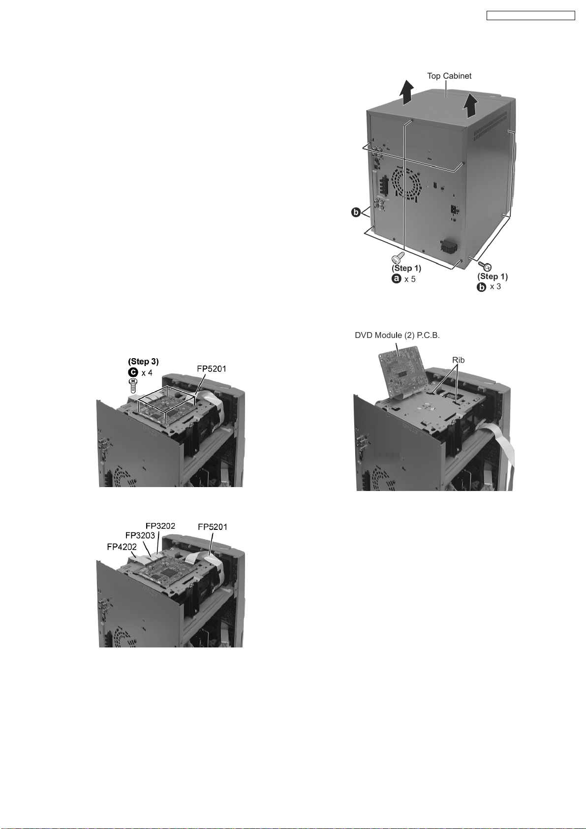
17.2. Disassembly of Top Cabinet
Step 1 Remove 3 screws each side and 5 screws at rear panel.
Step 2 Lift up both sides of cabinet ass’y, push the cabinet
ass’y toward the rear and remove the top cabinet.
SA-VK61DGC / SA-VK61DGCS
17.3. Disassembly of DVD Module (2) P.C.B.
· Follow the (Step 1) - (Step 2) of Item 17.2.
Step 1 Remove 4 screws.
Step 2 Detach FFC boards (FP5201, FP3202, FP3203 &
FP4202).
Step 3 Lift up DVD Module (2) P.C.B. as shown to remove it.
17.4. Disassembly for the Top Ornament Unit
(The DVD changer unit can be removed after the Top
Ornament Unit is removed)
· Follow the (Step 1) - (Step 2) of Item 17.2.
When opening the disc tray automatically (Using Power
Supply)
Step 1 Connect the AC power cord.
Step 2 Press the power button to power up the main unit.
Step 3 Press the OPEN/CLOSE button, the disc tray will be
open automatically.
31
Page 32

SA-VK61DGC / SA-VK61DGCS
Step 4 Release the 2 claws, and then remove the Top
Ornament Unit.
Step 1 Insert the gear tool into the hole on the underside of
changer chasis and then rotate in the direction of arrow. The
disc tray will be open.
Step 2 Release the 2 claws, and then remove the CD lid cover.
Step 5 Press the OPEN/CLOSE button, the disc tray will be
close.
[Open the disc tray manually (Using service tools)]
Step 3 Repeat Step 1 but rotate in anti-clockwise direction.
32
Page 33
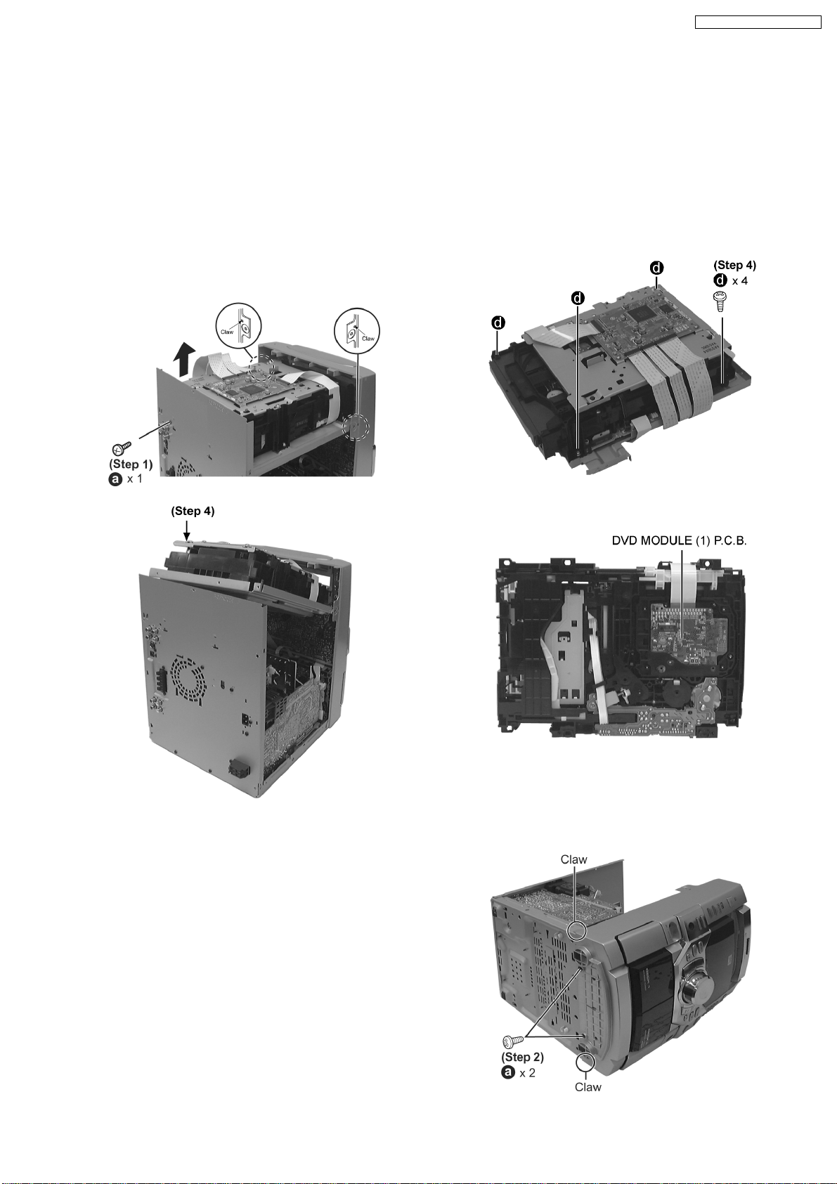
17.5. Disassembly for DVD changer unit
· Follow the (Step 1) - (Step 2) of Item 17.2.
· Follow the Disassembly for the Top Ornament Unit of Item
17.4.
Step 1 Detach FFC Boards (FP5201, FP3202, FP3203 &
FP4202).
Step 2 Remove 1 screw at rear cabinet as show below.
Step 3 Lift up the mechanism unit cover, and then push in the
mechanism unit cover.
Step 4 Release the claws of both ends, and then lift up the
DVD changer unit.
SA-VK61DGC / SA-VK61DGCS
17.5.1. Disassembly of the DVD Module
(1) P.C.B.
· Follow the (Step 1) - (Step 2) of Item 17.2.
· Follow the Disassembly for the Top Ornament Unit of Item
17.4.
· Follow the (Step 1) - (Step 4) of Item 17.5.
Step 1 Remove 4 screws.
Step 2 Remove the mechanism unit cover.
Step 3 Lay the unit.
Step 4 Connect the FFCs board from DVD Module (1) P.C.B..
17.6. Disassembly for Panel P.C.B., LED P.C.B. & Tact Switch P.C.B.
· Follow the (Step 1) - (Step 2) of Item 17.2.
· Follow the Disassembly for the Top Ornament Unit of Item
17.4.
Step 1 Lay the unit as shown below.
33
Page 34

SA-VK61DGC / SA-VK61DGCS
Step 2 Remove 2 screws at bottom chassis.
Step 3 Release the 2 claws, and then draw the front panel
ass’y forward.
· Disassembly of Panel P.C.B.
Step 4 Remove the 8 screws.
Step 5 Disconnect FFC board (CN601 & CN602).
Step 6 Draw the Panel P.C.B. forward to remove it.
· Disassembly of Tact Switch P.C.B. & LED P.C.B.
Step 7 Remove the volume knob.
Step 8 Disconnect connector W601B.
Step 9 Remove 6 screws.
Step 10 Draw Tact Switch P.C.B. forward.
17.7. Disassembly of Main P.C.B., Power P.C.B., Transformer P.C.B. &
Voltage Selector P.C.B.
· Follow the (Step 1) - (Step 2) of Item 17.2.
· Follow the Disassembly for the Top Ornament Unit of Item
17.4.
Step 1 Remove the 11 screws.
Step 2 Push the catch outwards & draw the rear panel
backwards to remove it.
· Disassembly of Power P.C.B.
−
− Follow the (Step 1) - (Step 2) of Item 17.2.
− −
−
− Follow the Disassembly for the Top Ornament Unit of
− −
Item 17.4.
−
− Follow the (Step 1) - (Step 4) of Item 17.5.
− −
−
− Follow the (Step 1) - (Step 4) of Item 17.6.
− −
Step 3 Detach connectors (CN601, CN602 and CN302).
Step 4 Lift up the Main P.C.B. to remove it.
Caution Note:
Avoid using/ exerted strong force when removing the Main
P.C.B.
34
Page 35
SA-VK61DGC / SA-VK61DGCS
Step 1 Remove the 4 screws.
Step 2 Detach wire.
NOTE:
Insulate Power P.C.B. with insulation material to avoid short
circuit.
· Disassembly of the Transformer P.C.B. & Voltage
Selector P.C.B.
−
− Follow the (Step 1) - (Step 2) of Item 17.2.
− −
−
− Follow the Disassembly for the Top Ornament Unit of
− −
Item 17.4.
−
− Follow the (Step 1) - (Step 4) of Item 17.5.
− −
Step 1 Remove 4 screws.
Step 2 Disconnect connector CN950 & CN951.
· Replacement of Power Amp IC
Step 1 Remove the 2 screws fixed to the Power Amplifier IC.
Step 2 Remove 2 screws fixed to the Power Amplifier IC and
Transistor Holders.
Step 3 Break the joint with a metal cutter as shown below.
Step 4 Unsolder the terminals of Power Amp IC, replace the
component.
35
Page 36
SA-VK61DGC / SA-VK61DGCS
Step 5 Fix back the bottom chasis with a screw as shown.
17.8. DVD Changer Unit Main Component Replacement Procedures
17.8.1. Replacement of the Traverse Deck
· Follow the (Step 1) - (Step 2) of Item 17.2.
· Follow the Disassembly for the Top Ornament Unit of Item
17.4.
· Follow the (Step 1) - (Step 4) of Item 17.5.
· Follow the (Step 1) - (Step 2) of Item 17.5.1.
Step 1 Insert the gear with hexagonal wrench into the hole.
Step 2 Rotate the hexagonal wrench in the direction of arrow
(clockwise), and then open the disc tray fully.
Step 3 With pressing the claw (A), rotate the hexagonal wrench
clockwise. (The slide plate R moves for a little amount.)
Step 4 Pressing the claw (B) in the direction of arrow (1), the
connection lever moves in the direction of arrow (2).
Step 5 Lift up the traverse deck ass’y.
36
Page 37
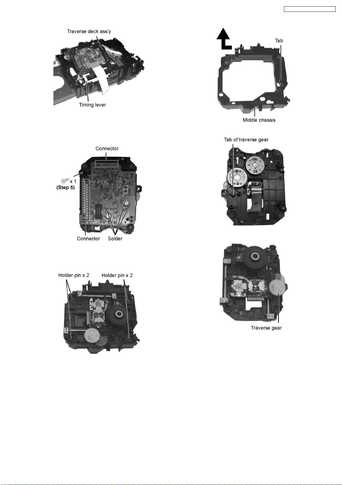
Step 6 Remove the traverse deck ass’y from the timing lever.
Caution:
When removing or inserting the traverse deck avoid touching
the OPU lens and pressing onto the turntable.
SA-VK61DGC / SA-VK61DGCS
Step 11 Disengage the tabs from the traverse gear.
Step 7 Remove 3 screws.
Step 8 Unsolder the motor terminals (4 points).
Step 9 Remove the holder pins.
Step 10 Remove the tab.
Step 12 Remove the traverse gear.
Step 13 Unscrew the screws.
Step 14 Remove the spring holders and the springs.
Step 15 Pull out the drive shaft and guide shaft.
37
Page 38
SA-VK61DGC / SA-VK61DGCS
Step 16 Remove the FFC board from the connector, and then
remove the DVD Module (1) P.C.B.
· Installation of the DVD Module (1) P.C.B. after
replacement
Step 1 Connect the FFC board.
Step 2 Install the DVD Module (1) P.C.B. in the traverse deck
ass’y.
Step 3 Remove 3 screws.
Step 4 Solder.
· Note for installation of the DVD Module (1) P.C.B.
· Installation for traverse deck ass’y
Step 1 Install the traverse deck ass’y to the timing lever.
Step 2 Align the boss of traverse deck ass’y with the slot of
traverse cam gear.
38
Page 39

Step 3 Force the claw of timing lever.
SA-VK61DGC / SA-VK61DGCS
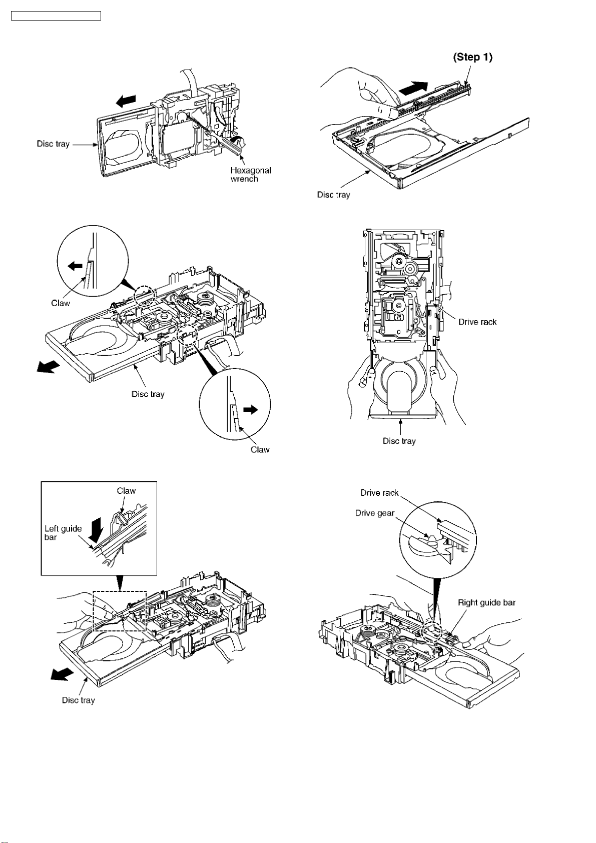
17.8.2. Replacement for the disc tray
Step 1 Remove 4 screws.
Step 2 Remove the upper plate.
Step 3 Remove 3 screws.
Step 4 Force the disc tray fully.
Step 5 With pressing the claw (B) in the direction of arrow (1),
force the connection lever in the direction of arrow (2).
Step 4 With lifting the claw in the direction of (1), draw the
clamp SW P.C.B. in the direction of arrow (2).
Step 5 Remove the mechanism cover.
39
Page 40
SA-VK61DGC / SA-VK61DGCS
Step 6 Insert the gear with hexagonal wrench into the hole.
Step 7 Rotate the hexagonal wrench in the direction of arrow,
and then open the disc tray fully.
Step 1 Slide the drive rack fully in the direction of arrow.
Step 8 Release the both claws, and then draw the disc tray.
Step 9 With forcing the left guide bar manually because the left
guide bar interfers with claw, draw the disc tray.
[Installation of the disc tray after replacement]
Step 2 Holding the drive rack not to move, install the disc tray.
Step 3 Align the drive rack with the drive gear.
NOTE:
Force the right guide bar of tray base manually not to move
upwards.
40
Page 41

Step 4 Holding the disc tray manually, push the disc tray in the
direction of the arrow.
17.8.3. Disassembly and reassembly for
mechanism base drive unit
· Follow the (Step 1) - (Step 9) of Item 17.8.2.
Step 1 Remove 3 screws.
SA-VK61DGC / SA-VK61DGCS
Step 5 Release the 2 claws, and then remove the bottom SW
P.C.B..
Step 2 Release the claw, and then remove the gear holder.
Step 3 Remove the belt and change gear spring.
NOTE:
Take care not to lose the change gear spring.
Step 4 Remove the pulley gear, change gear and UP/DOWN
gear.
Step 6 Install the tray lock spring to hook temporary.
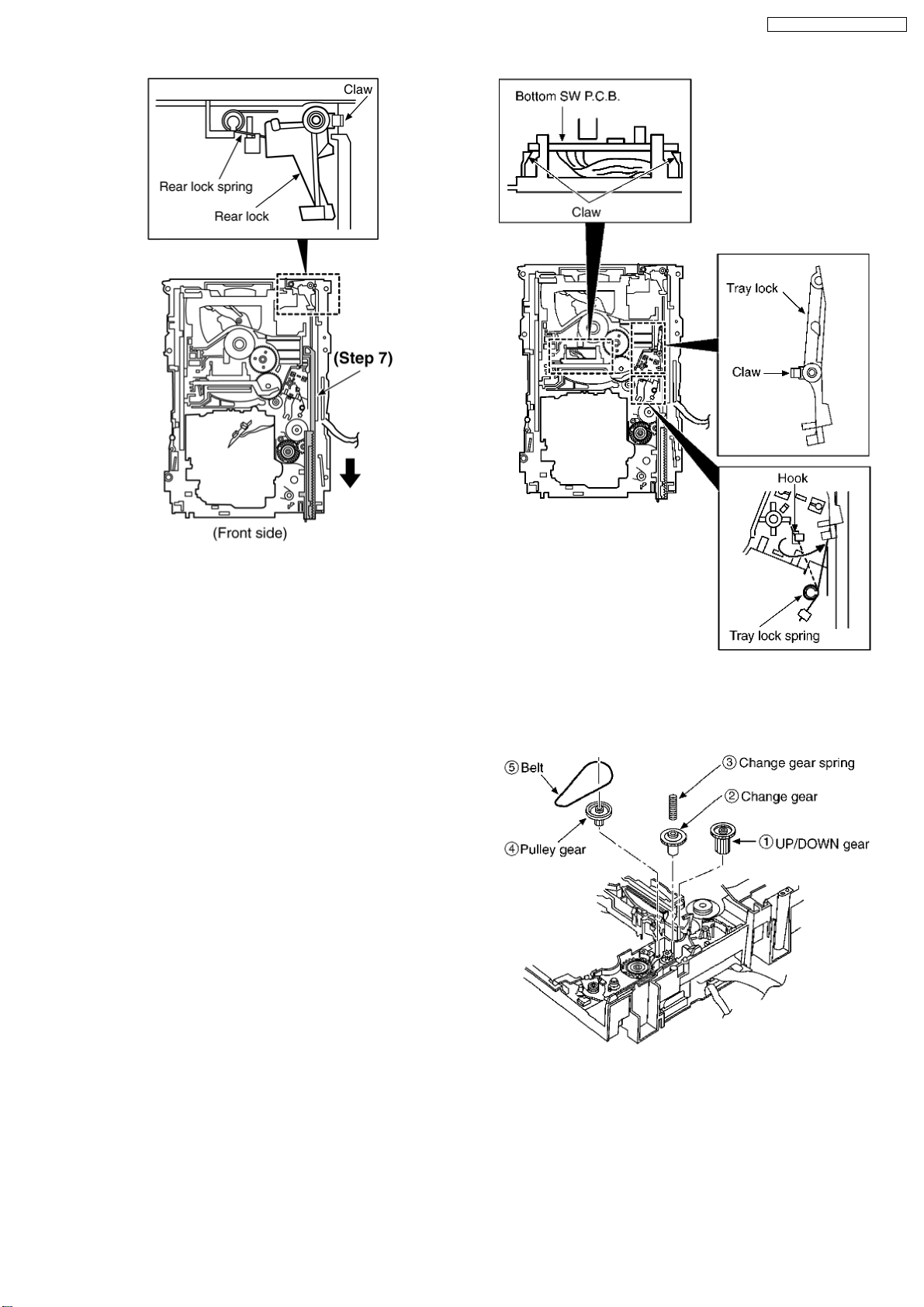
Step 7 Release the claw, and then remove the tray lock.
Step 8 Release the claw, and then remove the rear lock.
41
Page 42
SA-VK61DGC / SA-VK61DGCS
Step 11 Lift up the left end of spindle base unit in the direction
of arrow (1), and then remove the unit in the direction of arrow
(2).
Step 9 Pressing the claw (B) in the direction of arrow (1), force
the connection lever in the direction of arrow (2).
Step 10 Move the slide plate 1 to the end of stock side.
Step 12 Remove slide plate 1 and slide plate 2.
42
Page 43

Step 13 Remove the traverse relay gear, traverse cam gear
and drive gear.
SA-VK61DGC / SA-VK61DGCS
Step 3 Rotate the disc lever in the direction of arrow (1), draw
the disc lever.
[Dissassembly/reassembly for the spindle base unit]
Step 1 Draw the 5 disc spacers.
Step 2 Pushing the claw, slide the support plate in the direction
of arrow, and then remove it.
NOTE:
Take care not to lose the disc lever spring.
Step 4 Release the 2 claws, and then draw the relay gear B.
Step 5 Release the 2 claws as shown below.
43
Page 44
SA-VK61DGC / SA-VK61DGCS
NOTE:
Hold the loading stopper ass’y manually bacause it is flipped by
spring.
Step 6 Remove the cushion spring.
Step 7 Remove the loading stopper ass’y in the direction of
arrow.
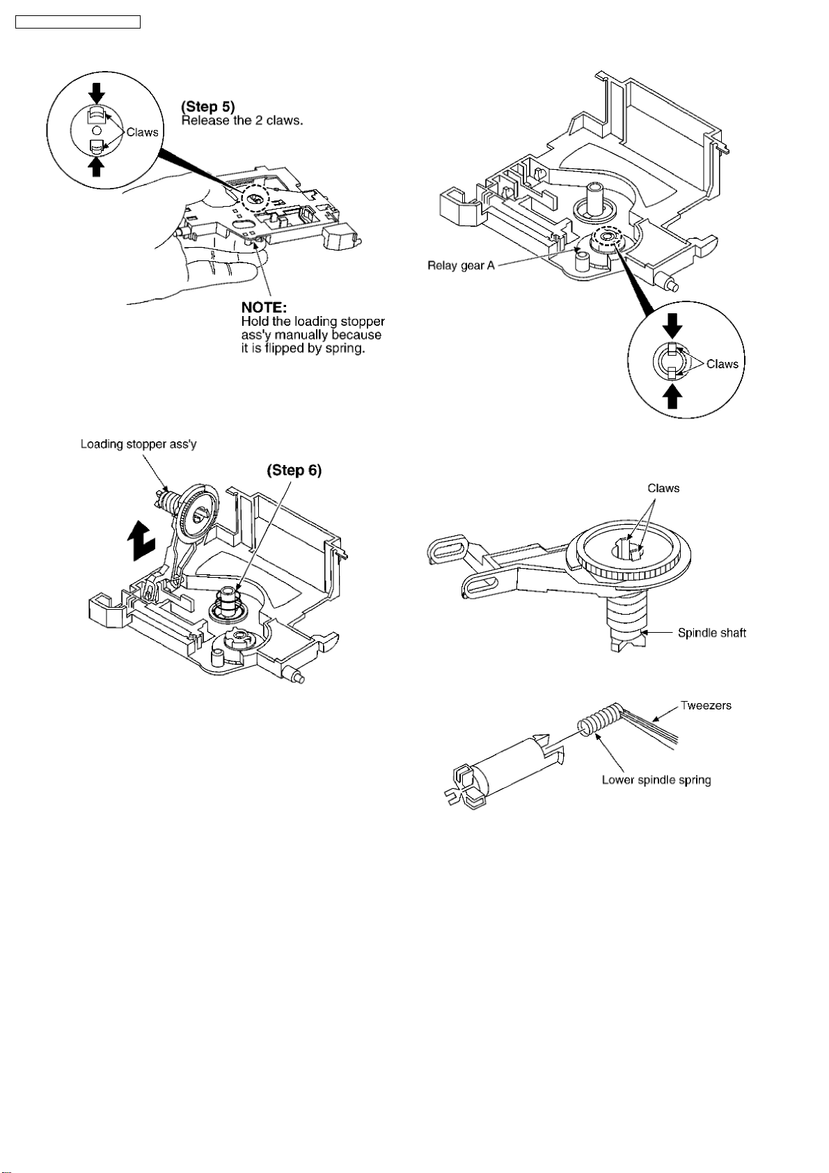
Step 8 Release the 2 claws, and then remove the relay gear A.
Step 9 Release the 2 claws, and then remove the spindle shaft.
Step 10 Remove the lower spindle spring with tweezers.
Step 11 Force the lower hook with thin tip of minus screwdriver.
44
Page 45

SA-VK61DGC / SA-VK61DGCS
spread the hold bars of loading stopper and remove the
UP/DOWN base.
[Installation for loading stopper ass’y]
Step 1 Align the claw of loading stoppers ass’y with the slot of
spindle base. (Caution should be exercised when alignment of
claw due to the size of claws.)
Step 12 Squeeze the shaft of lower hook, and then draw it.
Step 13 Rotate the lower spindle in the direction of arrow until
the lower spindle interferes with stopper.
Step 14 Insert the thin tip of minus screwdriver between the
lower spindle and UP/DOWN base, and then slacken the lower
spindle to release the stopper. Then, rotate the lower spindle
and remove it.
Step 2 Lower the loading stopper ass’y, and then align the
lower spindle with the trapezoid tooth of relay gear A.
Step 3 Force the loading stopper ass’y, latch the claw firmly.
Step 15 Rotate the UP/DOWN base at a 90° angle. Then,
[Reassembly for mechanism base drive unit]
45
Page 46

SA-VK61DGC / SA-VK61DGCS
Step 1 Install the traverse cam gear.
Step 2 Rotate the traverse cam gear to the direction of arrow.
Step 3 Install the drive gear and traverse relay gear.
*When installing the traverse relay gear, align the trapezoid
tooth of gear with tooth of traverse cam gear.
Step 4 Install the slide plate 2 to the mechanism base, and
then match to the connection lever.
Step 5 Install the slide plate 1 to the mechanism base, and
then match to the connection leve and align the trapezoid tooth
of traverse relay gear with the slide plate 1.
Step 6 Install the spindle base unit. (First, slide plate 1.)
46
Page 47
SA-VK61DGC / SA-VK61DGCS
Step 7 Move the slide plate 1 to forward fully.
Step 8 Install the rear lock. (The claw should be latched.)
Step 9 Install the bottom SW P.C.B.. (The claw should be
latched.)
Step 10 Install the tray lock. (The claw should be latched.)
Step 11 Remove the tray lock spring from hook,and then latch
to the tray lock.
Step 12 Install the UP/DOWN gear, change gear, change gear
spring, pulley gear and belt in the order of (1) - (5).
Step 13 Install the gear holder, and then tighten the screw (a).
47
Page 48

SA-VK61DGC / SA-VK61DGCS
Step 14 Install the tray base, traverse ass’y, mechanism cover
and upper plate.
[Operation check after servicing]
Check the proper operation of following items with gear and
hexagonal screwdriver.
1. Open/close of tray base.
2. Moving the tray base to the stock side.
3. UP/DOWN operation of spindle base unit.
4. UP/DOWN operation of traverse ass’y.
Step 4 Unsolder the plunger terminals (2 points).
Step 5 Unsolder the motor terminals (2 points).
17.8.4. Replacement for the motor ass’y
· Follow the (Step 1) - (Step 7) of Item 17.8.2.
Step 1 Install the belt temporarily.
NOTE:
Take care not apply the grease to the belt.
Step 2 Upset the CD loading unit.
Step 3 Remove 3 screws.
Step 6 Release the 2 claws (A), and then remove the Motor
P.C.B.
Step 7 Release the claw (B), and then remove the motor ass’y.
[Notice for motor ass’y installation]
1. Locate the name plate of motor to the traverse ass’y.
2. Align the hole of motor with the ribs.
48
Page 49
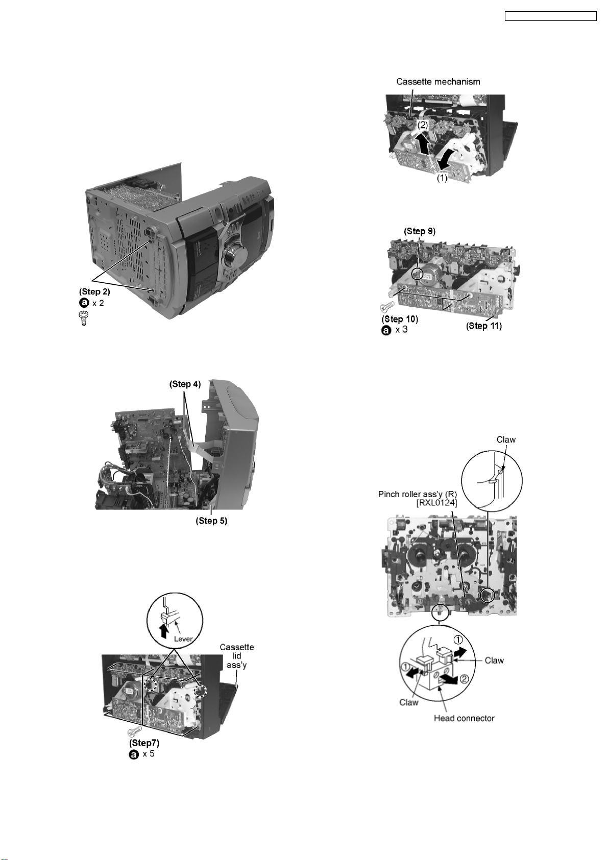
17.9. Disassembly of Deck Mechanism Unit
· Follow the (Step 1) - (Step 2) of Item 17.2.
· Follow the Disassembly for the Top Ornament Unit of Item
17.4.
· Follow the Disassembly for the DVD changer unit of Item
17.5.
Step 1 Lay the unit as shown.
Step 8 Tilt the cassette mechanism in the direction of arrow (1),
and then remove it in the direction of arrow (2).
SA-VK61DGC / SA-VK61DGCS
Step 2 Remove 2 screws.
Step 3 Release the 2 claws, and then draw the front panel
ass’y forward.
Step 4 Detach FFC Board (CN601 & CN602).
Step 5 Detach flat cable wire (CN1001).
Step 6 Push the lever upward, and then open the cassette lid
ass’y (For DECK1 and DECK2).
· Disassembly of Deck P.C.B.
Step 9 Unsolder the motor terminals.
Step 10 Remove 4 screws.
Step 11 Remove Deck P.C.B.
* The mechanism as shown below is for DECK1. For the
one of DECK 2, perform the same procedures.
Step 7 Remove the 5 screw.
· Disassembly of pinch roller ass’y & head block
Step 12 Release the 2 claws, and then remove the pinch roller
(R), (F).
Step 13 Release ther 2 claws, and then remove the head
connector.
49
Page 50

SA-VK61DGC / SA-VK61DGCS
Step 14 Remove 2 screws.
17.9.1. Replacement for the CD motor ass’y, capstan belt A, capstan belt B and winding
belt
Step 1 Release the 2 claws, and then remove the head
connector.
Step 2 Remove 6 screws.
Step 3 Remove the sub chassis.
Step 4 Remove 2 screws.
Step 5 Remove the flywheel R.
Step 6 Release the claw of tape side, and then remove the
winding lever and spring.
Step 7 Remove the flywheel F.
[Installation of the belt]
Step 1 The boss and marking should be positioned
horizontally.
50
Page 51
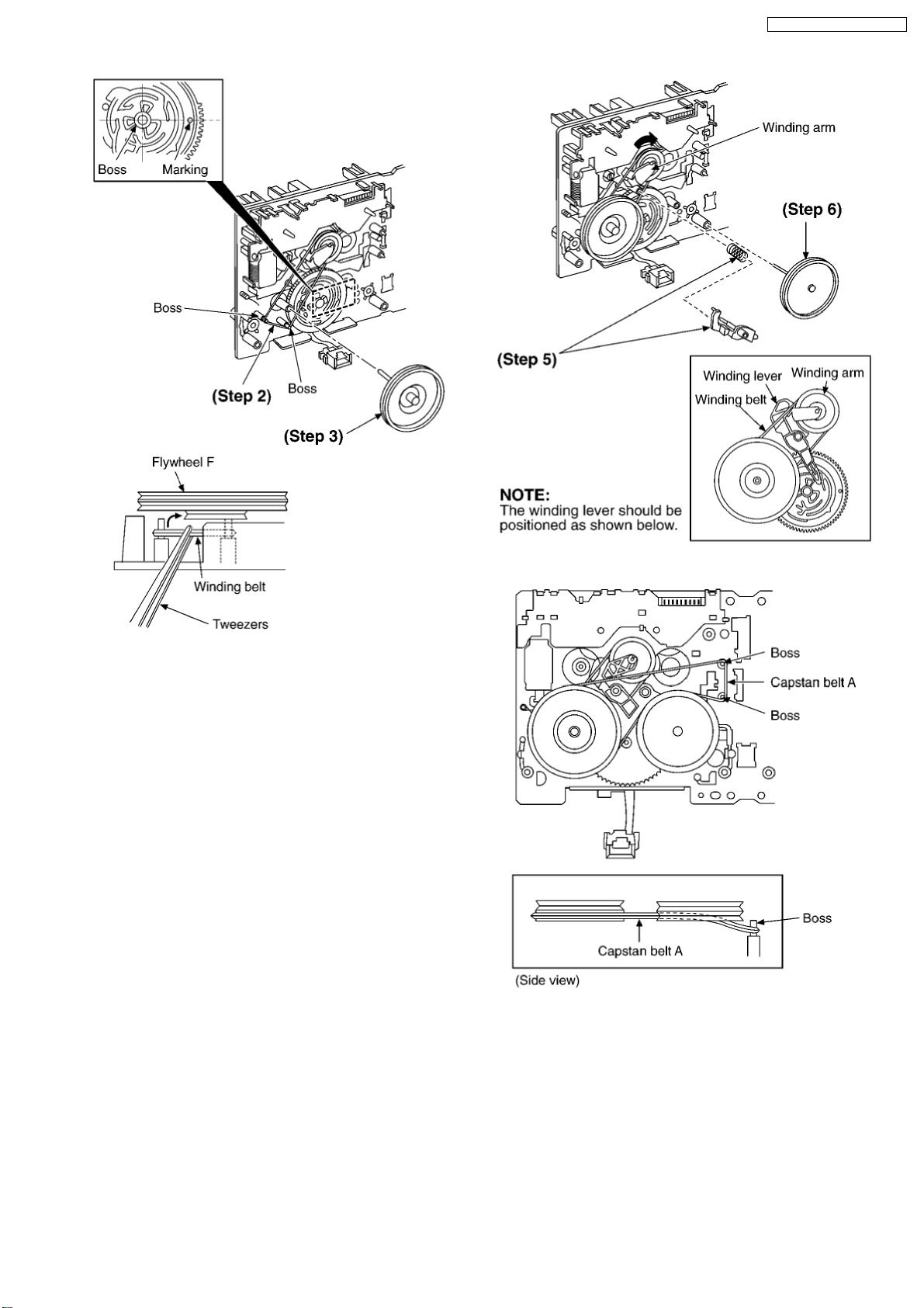
SA-VK61DGC / SA-VK61DGCS
Step 2 Put the winding belt on the pulley temporarily.
Step 3 Install the flywheel F.
Step 4 Put the winding belt on the flywheel F.
Step 5 Install the winding lever and spring while pressing the
winding arm in the direction of arrow.
Step 6 Install the flywheel R.
Step 7 Put the capstan belt A temporarily as shown below.
Step 8 Put the capstan belt B on the motor ass’y pulley.
Step 9 Install the sub chassis to the mechanism, and then
tighten screws.
51
Page 52

SA-VK61DGC / SA-VK61DGCS
17.10. Replacement for the cassette
lid ass’y
· Follow the (Step 1) - (Step 2) of Item 17.2.
Step 1 Force the lever upward, open the cassette lid ass’y. (For
DECK1 and DECK2)
Step 10 Remove 3 screws.
Step 11 Put the capstan belt B as shown below.
Step 12 Put the capstan belt A on the motor ass’y pulley.
Step 2 Lift up the cassette lid ass’y in the direction of arrow.
(For DECK1 and DECK2).
Step 3 Remove the cassette lid ass’y. (For DECK1 and
DECK2).
52
Page 53

17.11. Counter-measure for tape
trouble
· Follow the (Step 1) - (Step 2) of Item 17.2.
Step 1 If a cassette tape cannot be removed from the deck
since the tape is caught by the capstan or pinch roller during
playback or recording, rotate the flywheel F in the direction of
the arrow to remove the tape.
SA-VK61DGC / SA-VK61DGCS
Step 2 Force the lever upward and open the cassette lid ass’y.
Take the cassette tape off.
53
Page 54
SA-VK61DGC / SA-VK61DGCS
18 Measurements and Adjustments
18.1. Cassette Deck Section
· Measurement Condition
−
− Reverse-mode selector switch:
− −
−
− Tape edit: NORMAL
− −
−
− Make sure head, capstan and press roller are clean.
− −
−
− Judgeable room temperature 20 ± 5 °C (68 ± 9°F)
− −
· Measuring instrument
−
− EVM (DC Electronic volmeter)
− −
−
− Digital frequency counter
− −
· Test Tape
−
− Tape speed gain adjustment (3 kHz, -10 dB);
− −
QZZCWAT
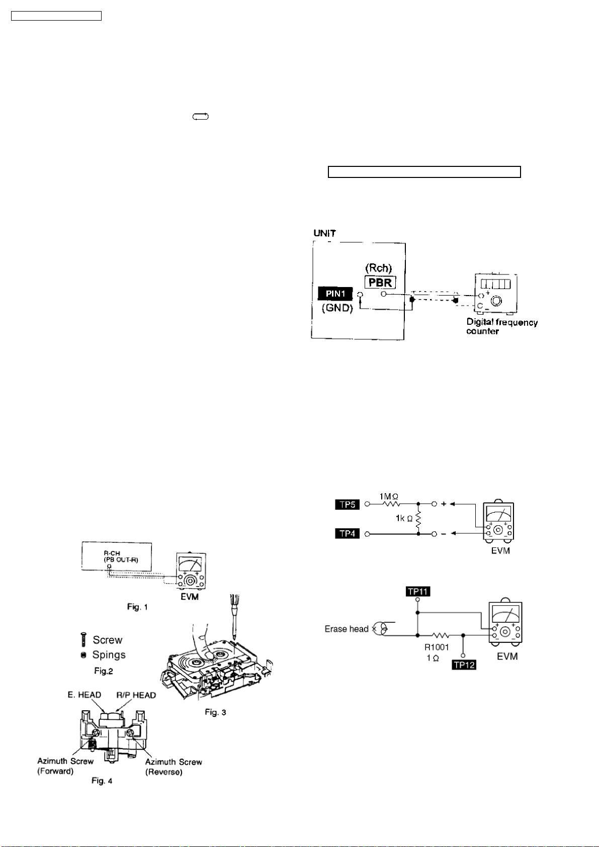
18.1.1. Head Azimuth Adjustment (Deck
1/2)
Caution:
· Please replace both azimuth adjustment screw and springs
simultaneously when readjusting the head azimuth. (shown
in Fig. 2) Even if you wish to readjust the head azimuth
without replacing the acrews and springs, a fine adjustment
to the azimuth screw and spring.
· Please remove the screw-locking bond left on the head
base when replacing the azimuth screw.
· If you wish to readjust the head azimuth, be sure to adjust
with adhering the cassette tape closely to the mechanism
by pushing the center of cassette tape with your finger.
(shown in Fig. 3)
1. Playback the azimuth adjustment portion (8 kHz, -20dB) of
the test tape (QZZCFM) in the forward play mode. Vary the
azimuth adjustment screw until the output of the R-CH (PB
OUT-R) are maximized.
2. Perform the same adjustment in the reverse play mode.
3. After the adjustment, apply screwlock to the azimuth
adjusting screw.
18.1.2. Tape Speed Adjustment (Deck 1/2)
1. Set the tape edit button to “NORMAL” position.
2. Insert the test tape (QZZCWAT) to DECK 2 and playback
(FWD side) the middle portion of it.
3. Adjust Motor VR (DECK 2) for the output value shown
below.
Adjustment target: 2940 ~ 3060 Hz (NORMAL speed)
4. After alignment, assure that the output frequency of the
DECK 1 FWD are within ±60 Hz of the value of the output
frequency of DECK 2 FWD.
Fig. 1
18.1.3. Bias and Erase Voltage Check
1. Set the unit “AUX” position.
2. Insert the Normal blank tape (QZZCRA) into DECK 2 and
the unit to “REC” mode (use “l REC/STOP” key).
3. Measure and make sure that the output is within the
standard value.
Bias voltage for Deck 2 14±4mV (Normal)
Erase voltage for Deck 2 80mV (Normal)
54
Fig. 2
Fig. 3
Page 55

18.1.4. Bias Frequency Adjustment (Deck
1/2)
1. Set the unit to “AUX” position.
2. Insert the Normal blank tape (QZZCRA) into DECK 2 and
set the unit to “REC” mode (l use “REC/STOP” key).
3. Adjust L1002 so that the output frequency is within the
standard value.
Standard Value: 97 ±8 kHz
18.2. Tuner Section
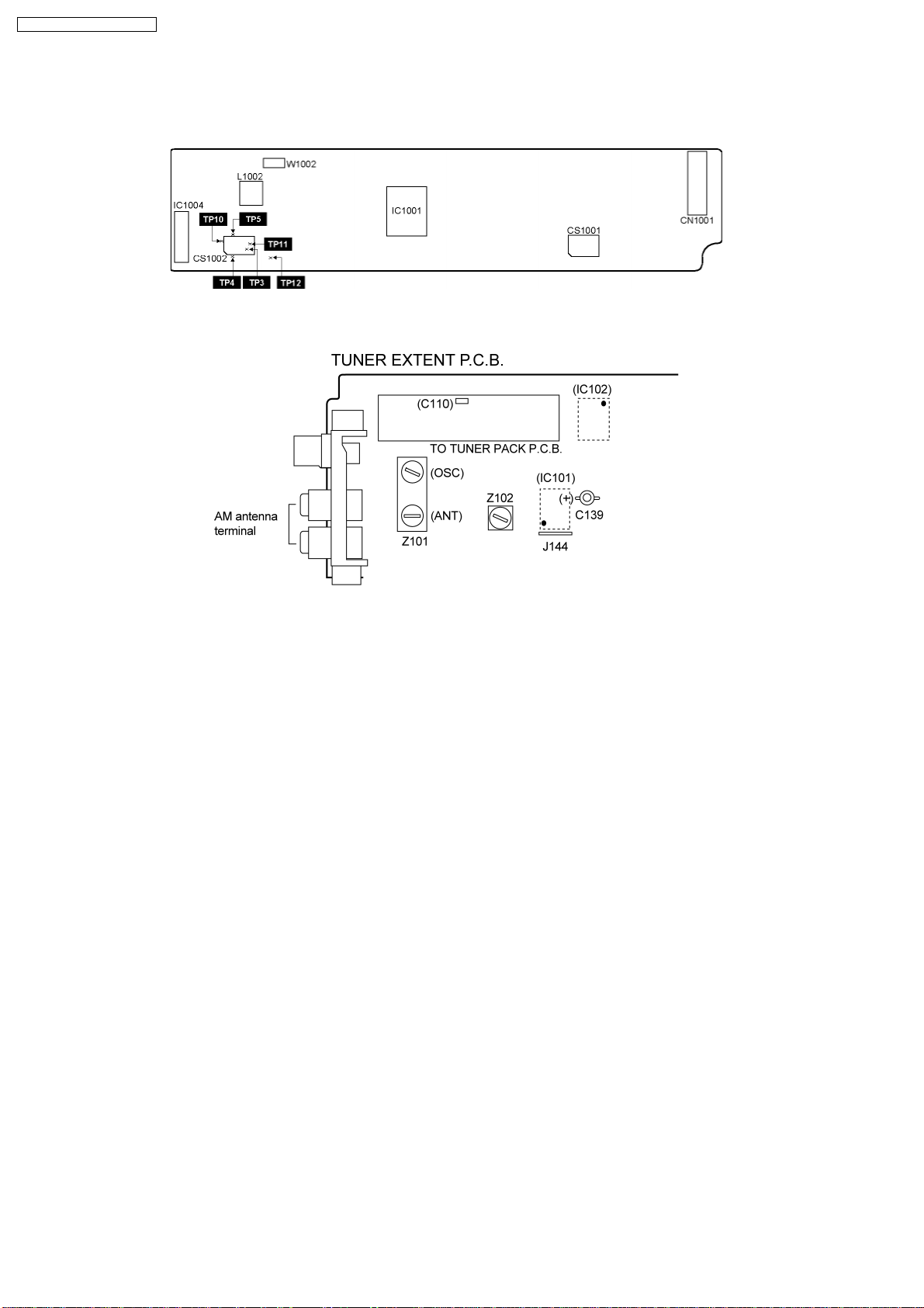
18.2.1. AM-IF Alignment
1. Connect the instrument as shown in Fig. 5.
2. Set the unit to AM mode.
3. Apply signal as shown in Fig. 5 from AM-SG.
4. Adjust Z102 so that the output frequency is maximized in
Fig. 6.
SA-VK61DGC / SA-VK61DGCS
Fig. 4
Fig. 5
Fig. 6
18.2.2. AM RF Adjustment
1. Connect the instrument as shown in Fig. 7.
2. Set the unit to AM mode.
3. Set AM-SG to 520kHz.
4. Receive 520kHz in the unit.
5. Adjust Z101 (OSC) so that the EVM-AC is maximized.
6. Set AM-SG to 600Hz.
7. Receive 600Hz in the unit.
8. Adjust Z101 (ANT) so that the EVM-SG is maximized.
9. Set AM-SG to 520kHz.
10. Receive 520kHz in the unit.
11. Adjust Z101 (OSC) so that the EVM-DC value is with
1.1±0.5V.
Fig. 7
55
Page 56
SA-VK61DGC / SA-VK61DGCS
18.3. Alignment Points
18.3.1. Cassette Deck Section
18.3.2. Adjustment Point
56
Page 57
19 Block Diagram
IC3051
C3ABPJ000017
64M SDRAM
SA-VK61DGC / SA-VK61DGCS
DQ0
DQ31
2,4,5,7,8,10,
11,13,31,33,34,
36,37,39,40,42,
45,47,48,50,51,
53,54,56,74,76,
77,79,80,82,83,85
2,3,5,6,8~10,12,
13,184,185,187,188,
190~193,196,197,
199~201,203~205,247,
249,251~253,255,256
MDQ0
MDQ15
DQM0
16,28,
59,71
207,208,
243,246
DQM0
DQM3
DQM3
A0
21,24~27,
60~66
210,212,214,
216,217,219,
220,227~229,
231,235
MA0
A11
WE
CAS
17
RAS
18
19CS20
BS022BS1
CLK
23
68
B
IC6251
C0CBCBE00003
REGULATOR
TO MAIN BLOCK
A
CMD
B
NRAS
234
238
NCSM
237
223
225
BA1
BA0
MCKI
MCK
232
MA11
NWE
239
242
NCAS
DSPCLK
5 4
IC6261
C0JBAA000001
INVERTER
1,2
62
P2
STATUS
5
4
IC6262
C0JBAA000001
INVERTER
1,2
63
P3
64
P1
MN2DS0002AP1
57
IC3001
AV DECODER
Page 58

SA-VK61DGC / SA-VK61DGCS
29,31,
33,35,
38,40,
42,44
DQ0
DQ7
1~8,
18~25
A15
DQ15
DQ14
DQ13
DQ8
30
41
45
43
A0
IC6301
RFKFMV71W160
16M FLASH
A20
10
9
26
XCE
DQ9
32,34,
36,39
DQ12
12
XRESET
A16
A17
A19
17
NC
48
16
13
XWE
XOE
NC
11
28
IC6201
C0EBE0000070
RESET IC
TO FG UNIT
FP2501
QR2045
SWITCH
19~22,27,28,
31,32,34~37,
40,41,44,45
33
NEXCE
EXADT0
EXADT15
94~97,
100~103
MONI(0)
MONI(7)
82
84
EXTRG0
85
EXTRG1
90
TRCST
TRCCLK
MN2DS0002AP1
17
39
EXADR20
38
EXADT19
EXADT17
IC3001
25
47
P15
EXADR16
AV DECODER
26
46
EXADR18
NEXOE
18
NEXWE
TRCDATA(0)
86~89
TRCDATA(3)
68
75
NRST
66
DRV5
FG
58
Page 59

MON
F
284
OPTICAL PICKUP
CDM HFM DVDM
5
15
LDOUT
F1
F2
10
LD
E
6
11
LDIN
2
LD
T1T2T3
4
T4
5
7
12
6
SA-VK61DGC / SA-VK61DGCS
SW
MON
F1
F2
13
RFP
RFN
14
10
8
11
FOCUS COIL
F- F+ T- T+
TRACKING COIL
M2501
M2502
M M
13
VO2-
14
12
VO1-
VO2+
VO1+
VIN1
BIAS1
1
2
VHALF
152
150
DAC1
137
AD1
11
Q5115
CD
SUPPLY
SWITCH
Q5225 Q5221
SWITCH SWITCH
VIN5
133
131
VIN10
LPC02
123
134
LPC2
122
130
VIN9
VIN6
Q5111
LD
SUPPLY
SWITCH
FILTER
135
146
AD2
LPC01
128
127
126
VIN1
VIN2
VIN3
125
129
124
VIN4
VIN7
VIN8
121
132
77
LPC1
DRV7
120
RFINP
RFINN
140
147
CSLFLT
17
5
18
VO3-
OPIN-
IC2501
C0GBG0000033
MOTOR DRIVE
VIN2
OPOUT
6
DAC0
9
148
78
AD0
3
VO3+
MUTE12
DRV8
4
OPIN+
23
71
VIN3
DRV1
16
15
VO4-
VO4+
TRIN
MUTE3
27
26
B
Q5211
SWITCH
73
74
70
DRV0
DRV4
DRV3
MN2DS0002AP1
59
IC3001
AV DECODER
Page 60

SA-VK61DGC / SA-VK61DGCS
2
VMUTE
Q52
INVERTER
SWITCH
WIDE
MIXL(R)
TO MAIN BLOCK
C
DVD_MUTE
IC50
C9ZB00000377
VIDEO BUFFER
PY IN
12
8
158
160
DAC1OUT
CB IN
14
161
DAC2OUT
VMUTE1
CR IN
5
163
DAC3OUT
CR OUT
CB OUT
PY OUT1
PY OUT2
MIX OUT2
MIX OUT1
Y IN
3
164
DAC4OUT
C OUT
Y OUT1
Y OUT2
C IN
DAC5OUT
32
25
24
17
19
22
21
29
30
Q4
CURRENT
CONTROL
Q7,Q8
CURRENT
CONTROL
JK301
S-VIDEO
C
G
Y
PR
7(8)
Q16
MUTING
SWITCH
PB
JK302
Y
IC4201
BCK
1
175
SRCK
C0FBBK000035
2CH D/A
CONVERTER
LRCK
DATA
3
2
176
174
LRCK
ADOUT3
13
60
VIDEO
X6501
7
8
IC6561
C1DB00000980
CLOCK
SW2501
IN SWITCH
GENERATOR
4
3
170
76
DRV6
14
55
BECLK
15
92
P7
OSCI
B
JK305
OPTICAL
B
72
DRV2
181
IECOUNT
SCK
16
10
172
EXTCK
VOUTL(R)
Q15
48
ZFLAGA
MDI
MC
ML
14
15
59
65
P0
P6
P5
MUTING
SWITCH
IC6351
C3EBGZ000001
EEPROM
(NOT SUPPLIED)
SCL
SDA
5
6
53
54
P8
P9
49
P13
MN2DS0002AP1
IC3001
AV DECODER
60
Page 61

SA-VK61DGC / SA-VK61DGCS
FM ANT
Z120
(RF AMP) Q1
17
5
6
(FM)
B
Q2
MIXER
Q3 Q4
BUFFER
OSC
8
CF201 CF202
Q101
FM IF AMP
IC101
LA1833NMNTLM
FM/ AM IF AMP
DET/ AM OSC MIX/
FM MPX
AM ANT
Z101
ANT
COIL
AM
AM
OSC
COIL
B
RCH
PHASE
DET
VCO
11
14
DECODER
STEREO
SWITCH
13
PILOT
CANCEL
PILOT
FFFFFF
DET
12
23
24
BUFFER
LEVEL
DET
FM
IF
1
22 21
ALC
AM
OSC
S-CURVE
FM
DET
REG
3
2
AM
MIX
AM/FM
IF
BUFFER
4 5
20 19 18
AM
RM AMP
AGC
AM
IF
COMP
TUNING
DRIVE
SD
6
DET
16 15
17
AM
REG
ST
7
9
8
10
B
Z102
AM
IFT
X102
ST/DO
SD
IC102
LC72131MDTRM
PLL FREQUENCY SYNTHESIZER
16
PHASE DETECTOR
CHARGE PUMP
UNLOCK
DETECTOR
17
18
11
UNIVERSAL
COUNTER
15
B
POWER ON
RESET
19 10
Q106
B
REFERENCE
DIVIDER
SWALLOW COUNTER
SHIFT REGISTER LATCH
7
TUNER
SUPPLY
SWITCH
B
(FM)
1/6,1/17,4 BITS
12 BITS PROGRAMMABLE
DIVIDER
6 9 8
12
1
X103
20
1
2
C2B
I/F
14
13
CE
2
3
DI
CL
4
DO
5
CE
DI
CL
ST/DO
A
TO DVD BLOCK
61
Page 62

SA-VK61DGC / SA-VK61DGCS
(DECK 1)
P.B. HEAD
(DECK 2)
R/P HEAD
LCH
LCH
4
2
IC1004
C1AA00000612
R/P SELECT
3
Q1017
D951
IC1001
AN7348S-E1
P.B. EQ/REC AMP/
ALC/TPS AMP
24(23)
1(2)
22(3)
21(4)
17(8)
15
6
19
(DECK 2)
ERASE HEAD
Q1001,Q1003
SWITCHING
(BEAT PROOF/
RECH)
MOTOR
MOTOR
SWITCH
M
Q608
SWITCH
(MOTOR)
Q615
PLUNGER
ON/OFF
SWITCH
PL971 PL970
NOR/CrO &
HI/LO LOGIC
LOGIC L/H
ALC
LOGIC
REC/PB
9
L1002
IC601
C1BB00000574
I/O EXPANDER
BP1
11
10
1M
14
1PL
RIPPLE
REJECTION
11
B
IC951
CNB13030R2AU
PHOTO
INTERRUPTOR
CONTROL
CIRCUIT
REGISTER
12-BIT SHIFT
20(5)
18(7)
14
10
16
13
BIAS OSC
CONTROL
Q1004~Q1007
LATCH
Q609
SWITCH
(REC:H)
DAT
CLK
REC
H1
DMT
OUTPUT BUFFER
2PL
IC971
CNB13030R2AU
PHOTO
INTERRUPTOR
2
3
12
13
9
15
B
Q614
PLUNGER
ON/OFF
SWITCH
Q1012
(Q1013)
Q1016
MUTING
DECK
MUTING
SWITCH
Q1014(Q1015)
BUFFER
AMP
SERC
D971
TO DVD BLOCK
SERA
C
Q1020
(Q1021)
MUTING
SWITCH
LIN(R)
DVD_MUTE
ST/DO
SD
CL
DI
CE
CMD
STATUS
DSPCLK
(HALF)
(RECINH_F)
(MODE)
(HALF)
(MODE)
S952
S951
25
77
PLLD_IF
80
SD
85
SERB
88
PLL_DA
92
PLL_CE
98
DVD_CMD
99
DVD_STA
100
DVDCLK
DECK1
FOR GC: C2BBHF000076
FOR GCS: C2BBHF000077
29
Z600
REMOTE SENSOR
Q612,
Q613
SWITCH SWITCH
26
RMT
DECK3
IC600
Q610,
Q611
MICROPROCESSOR
(RECINH_R)
S974
S971
Z971
INTERFACE
24
VOL_A
78
VR600
VOLUME JOG
DECK2
79
S972
VOL_B
S975
84
DVD_MUTE
62
Page 63

JK304
AUX
LINE
OUT
Q300
MUTING
CONTROL
Q301
MUTING
SWITCH
27(4)
29(2)
19(12)
24(7)
28(3)
21(10)
14
S3
S1
C0JZAS000004
ANALOG
SWITCH
C3
ST
S5
S2
S7
7(1)
KIA4558FEL
DUAL OP-AMP
IC301
IC302
SA-VK61DGC / SA-VK61DGCS
16
CK
17
DATA
33
32
IC702
75(74)
64(63),
65(62)
C1BB00000801
KARAOKE IC
34
22(9)
C2
25(6)
C1
5(3)
77
VR602
Q606,Q607
MIC
AMP
Q900
LIMITER
JK600
MIC1
JK900
MIC2
MIXL(R)
8
NJU_LAT
MUTE_L
CLOCK
95
SERE
DATA
54
53
97
SERF
LIN(R)
65(69)
IFDI
IFCK
SPEA
X700
3
XI
LIN4(R)
IC700
C2HBZC000013
DSP IC
/RST
50
94
DSP_RST/
DATA
CLOCK
BPL(R)
7(1)
5(3)
11(14)
4
XO
AOT1(2)
/CS
52
93
DSP_CS
KEYLAT
IC306
KIA4558FEL
DUAL OP-AMP
S901~S910
KEY SW
19
KEY2
S601~S605
KEY SW
20
KEY1
SEG1
42~45,47~50,
52~71,73~76
FL DISPLAY
SEG33
FL600
GRID1
30~40
GRID11
FOR GC: C2BBHF000076
FOR GCS: C2BBHF000077
FROM POWER
TRANSFORMER
IC600
MICROPROCESSOR
63
Page 64
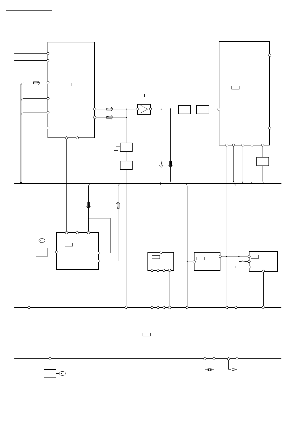
SA-VK61DGC / SA-VK61DGCS
41
40
CLOCK
DATA
DVD_PCNT
8
LIN(R)
BPL(R)
WIDE
Q321
15(13)
17(16)
B
SWITCH
3
39
LIN(R)
BYPASSL(R)
PORT3
LATCH
18
IC307
C1BB00000782
6 CHANNEL
VOLUME
PORT11PORT2
9
LVL1
IC701
M62456FPE1
DIGITAL SOUND
IFDI
CONTROLLER
IC703
C1BB00000574
HP_MUTE
2
3
I/O EXPANDER
DAT
CLK
3
10
SERA
SERA
MUTE_L
VMUTE
13
VMUTE
MUTE_L
5
IC603
6
BR93LC46FE2
EEPROM
4
(NOT SUPPLIED)
DSP_PCNT
9
Q522
MUTING
SWITCH
MUTE_H
3
15
MUTE_H
IC308
C0AABB000117
OP-AMP
31(32)
LOUT(R)
33
COUT
2
OUTL(R)
1(24)
10
LVL2
HPF1-1 (2)
22
NF2
2(23)
HPF1-2 (2)
Q308
Q314
FR_L(R)
MUTING
CONTROL
MUTING
SWITCH
2(6)
1(7)
OUTL(R)
8
IC603
C1BB00000086
SPECTRUM
ANALYSER
11
10
SPEA
12
17
HPL(R)
Q312
MUTING
CONTROL
SERC
2
Q317
MUTING
SWITCH
IC604
C1BB00000574
I/O EXPANDER
12
96
VOL_CS
Q700,Q701
94
SWITCH
DSP_RST/
91
MUTE_A
FOR GC: C2BBHF000076
FOR GCS: C2BBHF000077
B
83
82
SP_B
SP_A
IC600
MICROPROCESSOR
81
23
SP_C
SPE
86
SERC
CF1
CF2
15
16
X601
2
87
SERA
SERD
XCIN
XCOUT
13
12
X602
1
EECS
64
Page 65

SA-VK61DGC / SA-VK61DGCS
B
2
4
D2
Q1
POWER
SUPPLY
CONTROL
B
B
FILTER
B
L7L6
L9
IC2
C0CBADG00005
5V
REGUALTOR
IC6
C0CBADG00005
5V
REGULATOR
1
DCDET
LOAD
SW5
SW4
CD
2
4
B
FILTER
5
IC4
C0DBAMH00009
POWER
1
SUPPLY IC
OPEN
SW3
PUSH
SW2
PUSH
SW1
Q17
PCONT
SWITCH
Q18
PCONT
SWITCH
B
IC5
C0DBZHE00017
POWER
SUPPLY IC
IC1
C0GAM0000005
MOTOR DRIVE
IN1
5
REG
IN2
6
VREF4VCC7GND
1
Q6
SWITCH
Vs
OUT1
OUT2
B
Q101
CD MOTOR
SUPPLY SWITCH
Q100
PLUNGER MOTOR
SUPPLY CONTROL
SWITCH
B
5
8
2
10
IC3
C0DBAMH00009
POWER
SUPPLY IC
L4
Q5
CURRENT
LIMITER
Q801
SWITCH
B
M
RM1
B
D1
L8
DCDET
IC8
C0DBCFG00004
1.5V
REGULATOR
D806
B
IC9
C0CBADG00005
5V
REGULATOR
Q370~Q375
B
FAN
MOTOR
DRIVE
M
4
CHG_CW
5
CHG_CCW
6
CHG_PLGR
FOR GC: C2BBHF000076
FOR GCS: C2BBHF000077
IC600
MICROPROCESSOR
22
CHG_AD2
65
21
CHG_AD1
27
CHG_SW
3
CHG_HALF
7
DCDET
KEY3
SYNC
RESET
PCONT
S606~S612,S614
18
28
11
9
KEY SW
Q616
SYNC
SWITCH
Q600
RESET
SWITCH
Q605
PCONT
SWITCH
Q603,
Q604
POWER
B
SUPPLY
SWITCH
B
Page 66

SA-VK61DGC / SA-VK61DGCS
FR_L(R)
FAN
DCDET
KEY SW
HPL(R)
D526
21(20)
2
1
7
D979(D977)
L IN(R)
-VCC HI
+VCC HI
AC IN
IC500
RSN312H24-P
POWER HIC
FILTER
Q520,Q521
DCDET
SWITCH
Q540
REGULATOR
L OUT(R)
DISP HMUT
-VCC LOW
-Di SENS
+VCC LOW
+Di SENS
3(6)
D987(D984)
Q546~
11
19
-VD
18
+VD
D501
5
14
D500
4
13
D522,
D523
Q549,Q550
DCDET SWITCH,
POWER SUPPLY
Q541,Q542
REGULATOR
D520,
D521
Q548
SWITCH
Q545
SWITCH
Q543,
Q544
REGULATOR
LCH
JK953
FR
JK601
HEADPHONE
RCH
KEY SW
SYNC
SYNC
D968
RL502
Q952
REGULATOR
VOLTAGE
SELECTOR
S501
D962~D965
T502
SUB-
Z501
TRANSFORMER
F1
L500
JK500
AC INLET
B
Q951
REGULATOR
B
T501
FP950
F3
F4
MAIN TRANSFORMER
D951~D954
D969~D973
Q950
REGULATOR
D970
FP951
IC501
C5BA00000113
VOLTAGE
FAN
MUTE_H
REGULATOR
+Vin2
+Vin1
-Vin1
12
6
D957,D958
D528~D530
1
B
TO FL DISPLAY
Q953
PCONT
SWITCH
F2
E500
SIGNAL LINES
: MAIN SIGNAL LINE
: FM SIGNAL LINE
: FM OSC SIGNAL LINE
: FM /AM SIGNAL LINE
( ) Indicates the Pin No. of Right Channel.
: AM SIGNAL LINE
: AM OSC SIGNAL LINE
: AUX SIGNAL LINE
: CD SIGNAL LINE
: CD-DA (AUDIO /VIDEO) SIGNAL LINE
: DVD AUDIO SIGNAL LINE
: DVD VIDEO SIGNAL LINE
NOTE : Signal Lines are applicable to the Left Channel only.
: PLAYBACK SIGNAL LINE
: RECORD SIGNAL LINE
66
Page 67

20 Schematic Diagram
SA-VK61DGC / SA-VK61DGCS
(All schematic diagrams may be modified at any time with the
development of the new technology)
Note:
SW1 : Push Switch
SW2 : Push Switch
SW3 : Open Switch
SW4 : CD Switch
SW5 : Load Switch
S501 : Voltage Selector Switch
S601 : Power Switch
S602 : Dolby Pro Logic
S603 : Super Surround Switch
S604 : Deck 1/2 Switch
S605 : Rec Switch
S606 : CD Open/Close Switch
S607 : Disc 1 Switch
S608 : Disc 2 Switch
S609 : Disc 3 Switch
S610 : Disc 4 Switch
S611 : Disc 5 Switch
S612 : SSEQ Switch
S614 : SEQ Switch
S901 : Rew Switch
S902 : CD Play Switch
S903 : Tuner/Band Switch
S904 : FF Switch
S905 : Stop Switch
S906 : Deck 2 Switch
S907 : Tape Switch
S908 : AUX Switch
S909 : Deck 1 Switch
S910 : Display Switch
S951 : Mode Switch
S952 : Half Switch
S971 : Mode Switch
S972 : Half Switch
S974 : Recinh_R Switch
S975 : Recinh_F Switch
SW2501 : In Switch
VR600 : VR Volume Jog
VR602 : Mic Volume
· The voltage value and waveforms are the reference voltage
of this unit measured by DC electronic voltmeter (high
impedance) and oscilloscope on the basis of chassis.
Accordingly, there may arise some error in voltage values
and waveforms depending upon the internal impedance of
the tester or the measuring unit.
(( )) :CD <> :FM
repair.
· Cover the parts boxes made of plastics with aluminium foil.
· Put a conductive mat on the work table.
· Ground the soldering iron.
· Do not touch the pins of IC, LSI or VLSI with fingers directly.
· Importance safety notice :
Components identified by
characteristics important for safety. Furthermore, special
parts which have purposes of fire-retardant (resistors), highquality sound (capacitors), low-noise (resistors), etc. are
used. When replacing any of components, be sure to use
only manufacturer´s specified parts shown in the parts list.
Caution !
IC, LSI and VLSI are sensitive to static electricity.
Secondary trouble can be prevented by taking care during
mark have special
67
Page 68
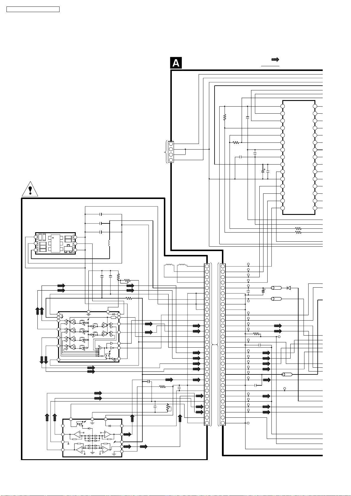
SA-VK61DGC / SA-VK61DGCS
20.1. (A) DVD Module (1) Circuit
SCHEMATIC DIAGRAM-1
DVD MODULE (1) CIRCUIT
IC2501
C0GBG0000033
MOTOR DRIVE
: CD-DA SIGNAL LINE
: +B SIGNAL LINE
OPTICAL PICKUP UNIT
HFM
LDGND
1
C4
LDIN
L1
2
R1
C1
3.0V
3
R2
LC
MODULE
VREF
VCC
T1
T2
T3
T4
MON
C2
C3
Q1
DVDM
2
3
x1
4
x2.75
x1
5
x2.75
x1
6
x2.75
x1
7
x2.75
8
NC
3
F1
4
(60kW)
VREF
5
E
6
LDGND
6
LDOUT
5
LDGND
4
(160kW)
17K
17K
17K
17K
CDM
C002
22P
C001
0.1
C003
0.22
0.1
C004
GND LDGND
Tr1
17K
Tr2
17K
Tr3
Tr4
GND LDGNDMON
Pmon
P2
P3
P4
P7
P8
P9
(160kW)
P1P6P5
P10
C005
x1
x2.75
x1
x2.75
1212
(60kW)
L001
0.1
161
LD
BIAS
x1
x1
Mon
LD
BK1005H5601-T
VR001
0
15K
R001
R004 0
LD
15
SW
14
F2
13
F1
12
RFN
11
RFP
10
GND
9
LD
11
F2
10
VCC
9
F
8
GND
7
FG UNIT
C008
0.1
C009
0.1
TO
FP2501
R002
VR002
1K
0
FOCUS
COIL
FG3
1
FG2
2
FG2
3
FG1
4
TRACKING
COIL
C007
0.1
BIAS1
1
2
C2504
0.1
LB5106
LB5105
VIN1
VIN2
3
4
OPIN+
OPIN-
5
6
OPOUT
7
GND(Pre)
FIN
VCC(ch1,2)
8
9
MUTE12
GND(ch1,2)
10
11
VO2-
12
VO2+
13
VO1-
VO1+
14
R2505 82K
R2504 82K
D5151
MA2J72800L
TC5115
LB5101
J0JHC0000045
TC5107
IC2501
R2502
15K
C2507 0.1
R2503
15K
C2508
0.1
T+
30
30
29
28
27
26
25
24
23
22
21
20
19
18
17
16
15
14
13
12
11
10
9
8
7
6
5
4
3
2
1
F+
29
F-
28
T-
27
3.3VHFM
26
GND
25
LD+(DVD)
24
GND
23
GND
22
RFP
21
RFN
20
F1(DVD)
19
F2(DVD)
18
GAINH/L
17
PIN(DVD)
16
VREF2.2(DVD)
15
TA(DVD)
14
TD(DVD)
13
TC(DVD)
12
TB(DVD)
11
VCC5V
10
FE1
9
GND
8
LD+(CD)
7
T1(CD)
6
VREF2.2(CD)
5
FE(CD)
4
T2(CD)
3
PIN(CD)
2
GND
1
C2506
0.1
C2501
TC5125
TC5124
TC5123
TC5122
TC5121
C5151
0.1
TC5120
TC5119
TC5118
TC5117
TC5116
R5124 4.7K
TC5114
C5123 0.1
TC5113
TC5112
TC5111
TC5110
TC5109
TC5108
C5102 0.1
TC5106
TC5105
TC5104
TC5103
TC5101
6.3V220P
J0JBC0000015
C5152
10V10
J0JBC0000015
LDCNT
MUTE3
TRIN
BIAS2
LDIN
VIN3
PREVCC
VCC(ch3,4)
MUTE4
GND(ch3,4)
VO3-
VO3+
VO4-
VO4+
28
27
26
25
24
23
22
FIN
21
20
19
18
17
16
15
FP5101
68
Page 69
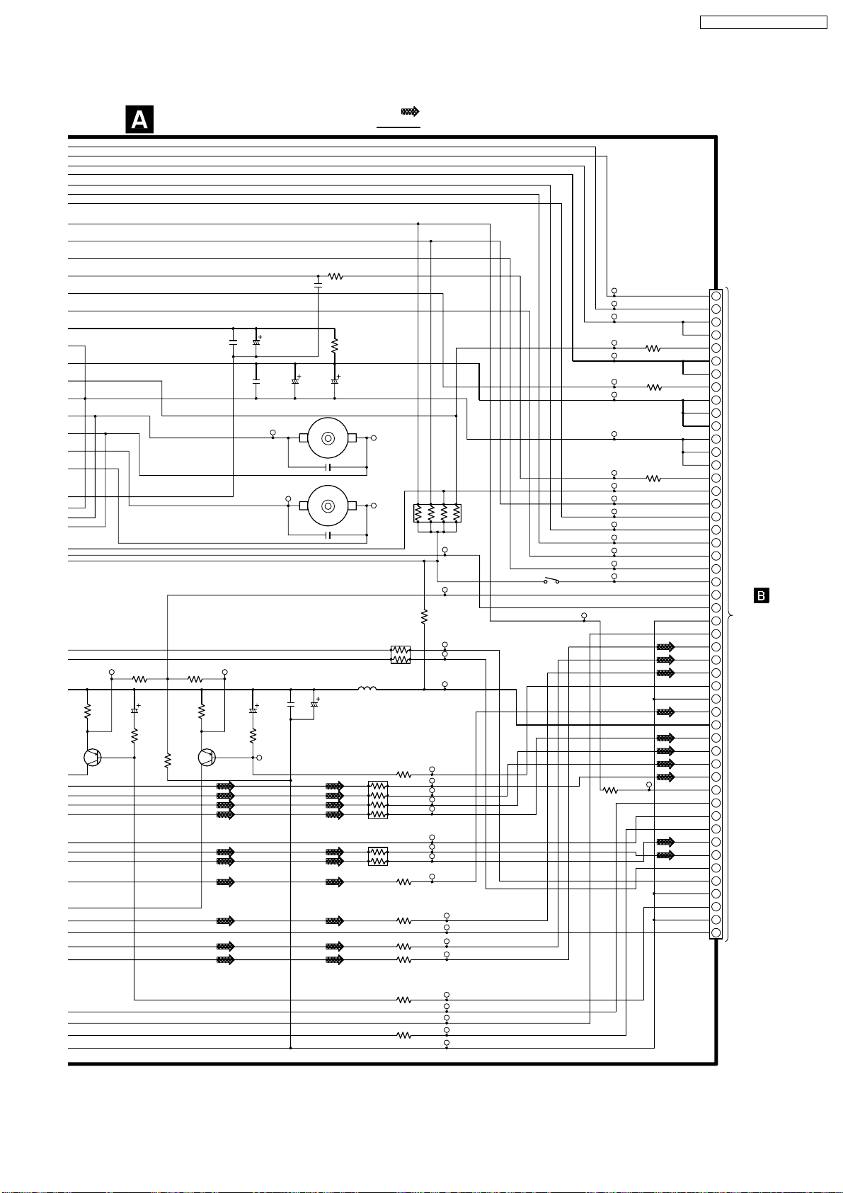
SCHEMATIC DIAGRAM-2
DVD MODULE (1) CIRCUIT
C2513
0.1
TC5130 TC5129
R5117
47K
R5112
27
C5 111
6.3V47
R5 111
2.2
Q5111 Q5115
R5114
22K
R5113
R5116
27
47K
C5115
6.3V47
R5115
2.2
C2503
16V22
C2505
0.1
TC2522
C5103
0.1
TC5127
TC2525
C2510
0.1
C2509
16V10P
R2501
100
R2507
6.8
C2502
16V100
M2501
SPINDLE
MOTOR
C2511 0.1
M2502
TRAVERSE
MOTOR
C2512 0.1
L5101
ELJEA100KF
C5101
16V10P
Q5 111
B1BDF000004
LD SUPPLY SWITCH
Q5115
B1BDF000004
CD SUPPLY SWITCH
TC2523
TC2524
RA5101
(56 x 2)
R5103 56
RA5102
(56 x 4)
RA5103
(56 x 2)
R5101 56
R5121 56
R5122 56
R5123 56
: CD-DA SIGNAL LINE
: +B SIGNAL LINE
RA2501
(47K x 4)
TP5115
CP5105
R5105
0
TP5119
TP5120
TP5130
TP5132
TP5126
TP5127
TP5128
TP5129
TP5124
TP5121
TP5122
TP5131
TP5133
TP5116
TP5134
TP5135
SW2501
CP5104
R5120
0
TP5101
TP5102
TP5103
TP5104
TP5113
CP5102
TP5105
TP5106
CP5103
TP5107
TP5108
CP5101
TP5109
TP5110
TP5111
TP5112
TP5114
TP5117
R5107
0
R5108
0
R5109
0
SA-VK61DGC / SA-VK61DGCS
FG1
1
FG3
2
DGND
3
DGND
4
MUTE4
5
D+5V
6
D+5V
M+9V
M+9V
M+9V
MGND
MGND
MGND
TRAYREF
MUTE12
MUTE3
DMV
FOIN
TRIN
SPDIN
TRVIN
INSW
LDCUR
VHALF
AGND
PIN(CD)
T2(CD)
FE2(CD)
T1(CD)
LPCO2
AGND
FE1(CD)
VCC+5V
TB(DVD)
TC(DVD)
TD(DVD)
TA(DVD)
TRAY/TRV
VREF2.2V
PIN(DVD)
GAINH/L
F2(DVD)
F1(DVD)
RFN
RFP
AGND
LPCO1
AGND
3.3VHFM
7
8
9
10
11
12
13
14
15
16
17
18
19
20
21
22
23
24
TO
25
DVD MODULE 2
(FORE) CIRCUIT
26
(FP5201) ON
27
SCHEMATIC
DIAGRAM-3
28
29
30
31
32
33
34
35
36
37
38
39
40
41
42
43
44
45
46
47
48
49
50
FP5102
TRAYIN(D+5V)
R5102 56
R5152 1K
69
TP5118
TP5125
TP5136
TP5123
TP5137
Page 70
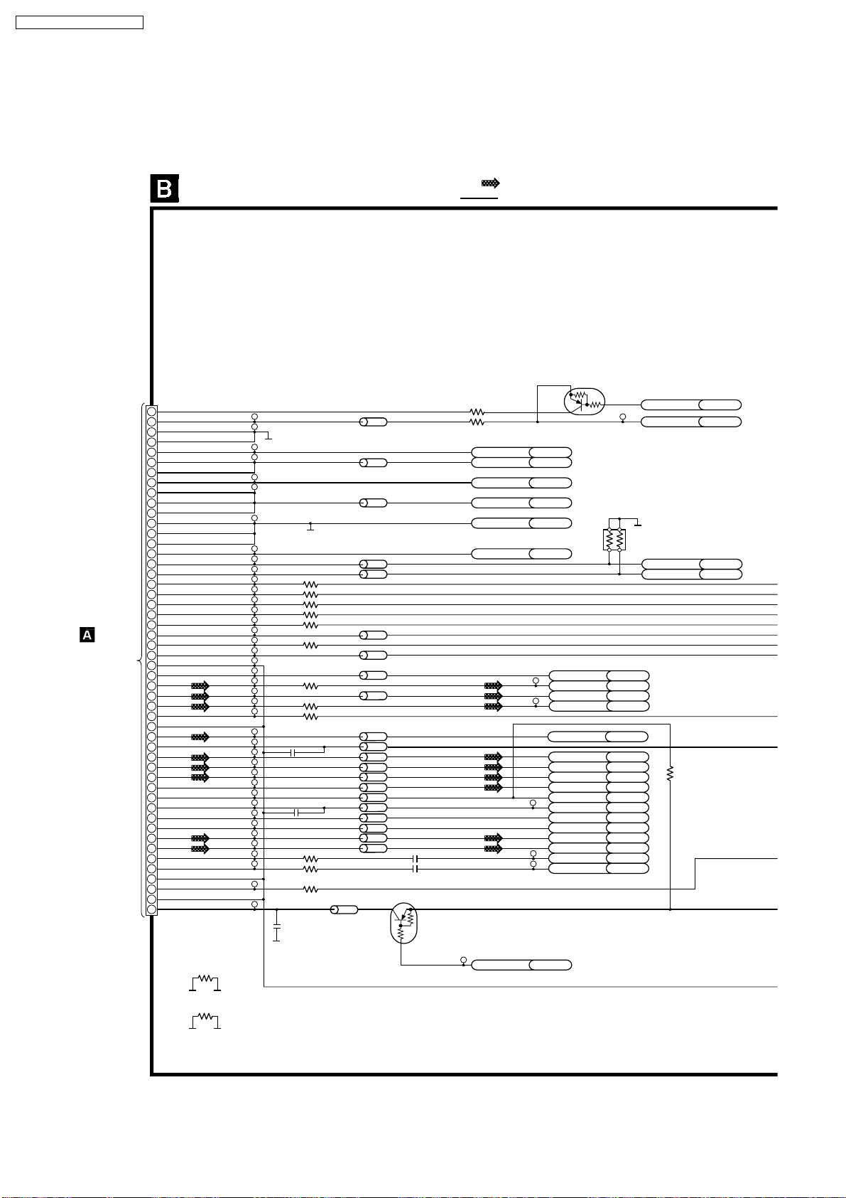
SA-VK61DGC / SA-VK61DGCS
20.2. (B) DVD Module (2) Circuit
SCHEMATIC DIAGRAM - 3
DVD MODULE 2 (FORE) CIRCUIT
FG1
TO
DVD MODULE 1
CIRCUIT
(FP5102) ON
SCHEMATIC
DIAGRAM - 2
FP5201
50
FG3
49
DGND
48
DGND
47
MUTE4(DGND)
46
D+5V
45
D+5V
44
TRAYIN(D+5V)
43
M+9V
42
M+9V
41
M+9V
40
MGND
39
MGND
38
MGND
37
TRAYREF(MGND)
36
MUTE12
35
MUTE3
34
DMV
33
FOIN
32
TRIN
31
SPIN
30
TRVIN
29
IN-SW
28
LDCUR
27
VHALF
26
AGND
25
PIN(CD)
24
T2(CD)
23
FE2(CD)
22
T1(CD)
21
LPCO2
20
AGND
19
FE1(CD)
18
VCC5V
17
TB(DVD)
16
TC(DVD)
15
TD(DVD)
14
TA(DVD)
13
TRAY/TRV(VREF2.2V)
12
VREF2.2V
11
PIN(DVD)
10
GAINH/L
9
F2(DVD)
8
F1(DVD)
7
RFN
6
RFP
5
AGND
4
LPCO1
3
AGND
2
3.3VHFM
1
TC5240
TC5239
TC5238
TC5237
TC5236
TC5235
TC5234
TC5233
TC5232
TC5231
TC5230
TC5229
TC5228
TC5227
TC5226
TC5225
TC5224
TC5223
TC5222
TC5221
TC5220
TC5219
TC5218
TC5217
TC5216
TC5215
TC5214
TC5213
TC5212
TC5211
TC5210
TC5209
TC5208
TC5207
TC5206
TC5205
TC5204
TC5203
TC5202
TC5201
R1
0
R2021 15K
R2015 J0JBC0000015
R2017 J0JBC0000015
R2011 J0JBC0000015
R2013 J0JBC0000015
R2023 15K
R5234 2.2K
R5233 2.2K
R5202 0
C5203 0.1
C5202 0.1
R5232 J0JCC0000119
R5231 J0JCC0000119
R5201 0
C5201
0.1
LB5235 J0JBC0000015
LB5233 J0JHC0000045
LB5231 J0JHC0000045
LB5229 J0JBC0000015
LB5228 J0JBC0000015
LB5222 ERJ3GEY0R00V
LB5220 J0JBC0000015
LB5219 J0JCC0000119
LB5217 J0JCC0000119
LB5215 J0JCC0000119
LB5214 J0JHC0000045
LB5213 J0JCC0000119
LB5212 J0JCC0000119
LB5211 J0JCC0000119
LB5210 J0JCC0000119
LB5209 J0JBC0000015
LB5208 J0JBC0000015
LB5207 J0JCC0000119
LB5206 J0JBC0000015
LB5205 J0JCC0000119
LB5204 J0JCC0000119
LB5201
J0JBC0000015
C5232 0.1
C5231 0.1
R2046
220
R2045
82K
Q5211
UNR212100L
SWITCH
CP5211
: CD-DA SIGNAL LINE
: +B SIGNAL LINE
QR2045
UNR511M00L
SWITCH
MUTE4 HIND
D+5V HIND
TRAYDRV HIND
M+9V HIND
MGND HIND
TRAYREF HIND
CP5232
CP5231
TC5244
TC5243
TC5242
HFMON DV1
QR2045
CP2041
LPC2 DV1
VIN10 DV1
VIN6 DV1
VIN9 DV1
VIN5 DV1
VIN4 DV1
VIN3 DV1
VIN2 DV1
VIN1 DV1
TRAY/TRV HIND
VREFH DV1
LPC1 DV1
GAINH/L DV1
VIN8 DV1
VIN7 DV1
RFINN DV1
RFINP DV1
RA2025
(47K x 2)
FG1 DV1
FG3 DV1
MUTE12 DV1
MUTE3 DV1
R5235
1K
R4
0
70
Page 71
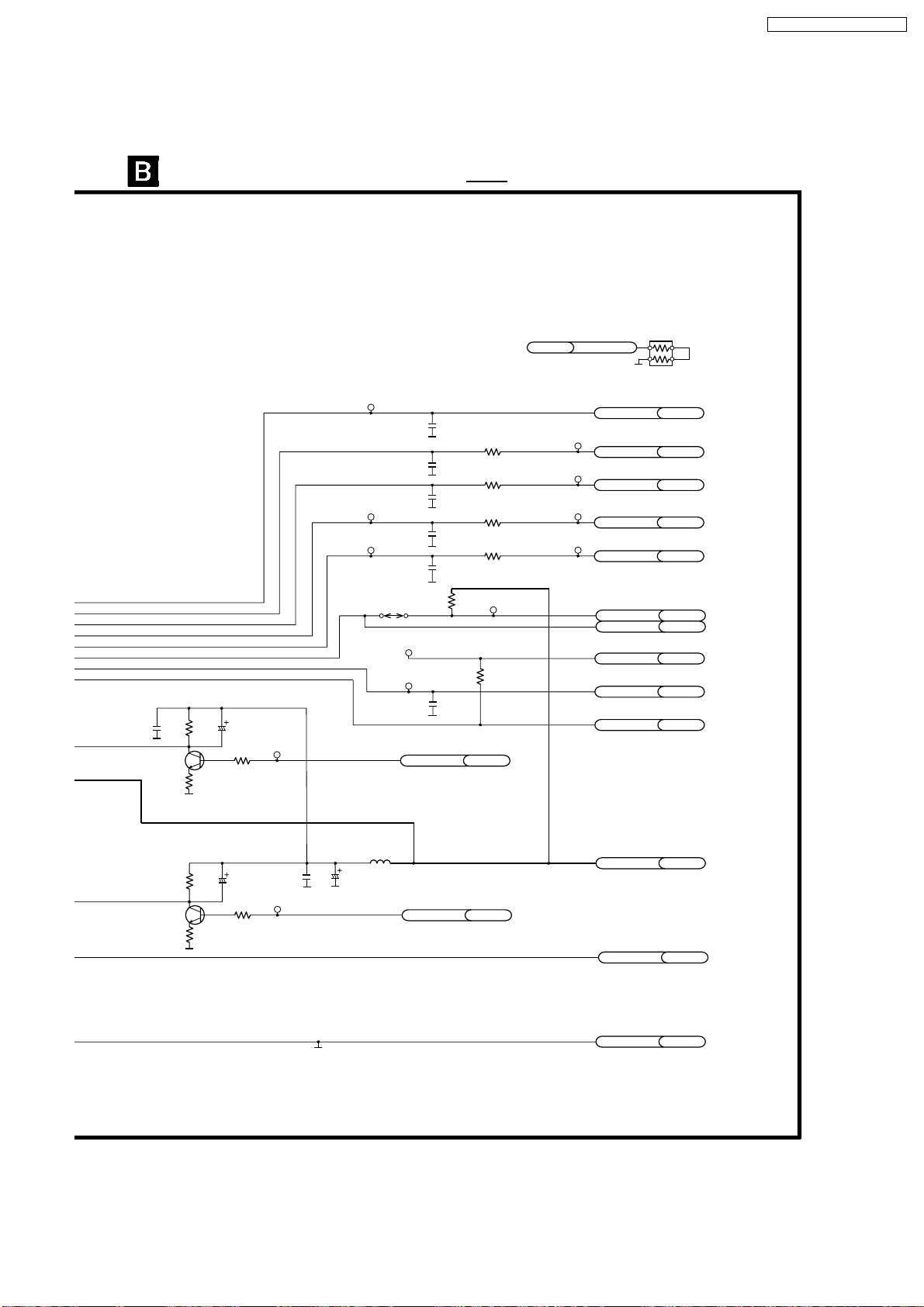
SCHEMATIC DIAGRAM - 4
SA-VK61DGC / SA-VK61DGCS
DVD MODULE 2 (FORE) CIRCUIT
C5225
R52261KC5226
0.1
R5227
330
25V4.7
R5225
0
Q5225
Q5225
2SD1819A0L
SWITCH
CP5225
CP2019
CP2011
CP2013
K2041
0
CP2020
CP2021
C2021
4700P
C2015
1000P
C2016
820P
C2011
0.1
C2012
0.1
R2041
47K
LPCO2 DV1
C2023
1000P
CP2023
: +B SIGNAL LINE
R2016
8.2K
R2018
8.2K
R2012
7.5K
R2014
7.5K
R2022
10K
DV1 KMODE
CP2016
CP2018
CP2012
CP2014
RA6201
(4.7K x 2)
AD0 DV1
DAC0 DV1
DAC1
SPDRV DV1
TRSDRV DV1
SW DV1
TRV-SW+ HIND
AD1 DV1
AD2 DV1
VHALF DV1
DV1
R5222
1K
R5223
330
C5223
25V4.7
R5221
0
Q5221
Q5221
2SD1819A0L
SWITCH
CP5221
C5222
0.1
G1C100K00020
C5221
6.3V33
L5221
A+5V HIND
LPCO1 DV1
D+3.3V DV1/HIND
AGND HIND/DV1
71
Page 72
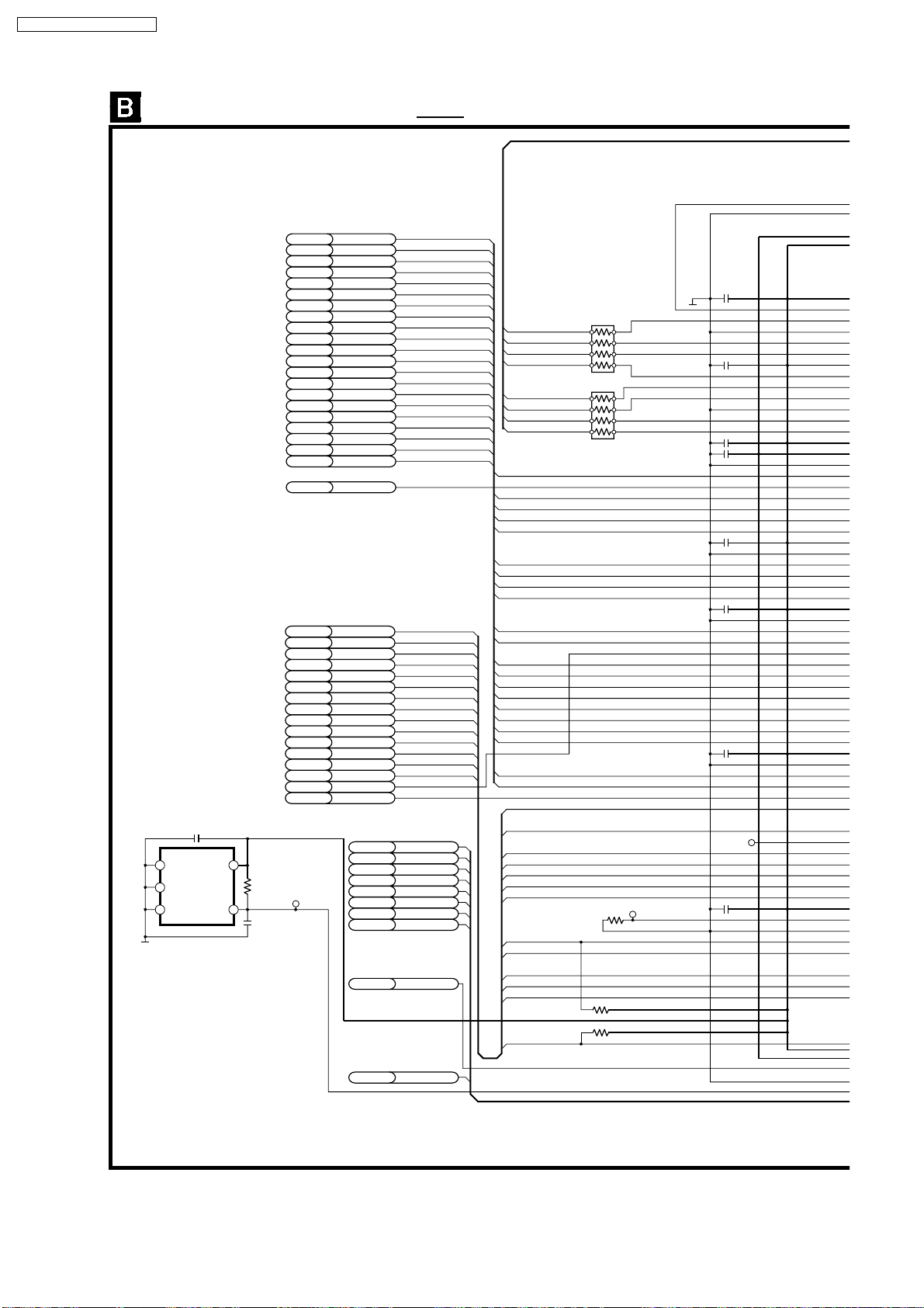
SA-VK61DGC / SA-VK61DGCS
SCHEMATIC DIAGRAM - 5
DVD MODULE 2 (DV1) CIRCUIT
HIND EXADR (20)
HIND EXADR (19)
HIND EXADR (18)
HIND EXADR (17)
HIND EXADR (16)
HIND EXADT (15)
HIND EXADT (14)
HIND EXADT (13)
HIND EXADT (12)
HIND EXADT (11)
HIND EXADT (10)
HIND EXADT (9)
HIND EXADT (8)
HIND EXADT (7)
HIND EXADT (6)
HIND EXADT (5)
HIND EXADT (4)
HIND EXADT (3)
HIND EXADT (2)
HIND EXADT (1)
HIND EXADT (0)
HIND NEXWE
HIND P (15)
AD AMUT
AD 25BSY(AC3H)
FORE KMODE
HIND SCL
HIND SDA
AD CLKSEL
AD SBT1
AD SBO1
AD SBI1
HIND DSPCLK_DV1
HIND STATUS_DV1
HIND CMD
HIND STBDAC
R6201
4.7K
100P
HIND NEXCE
HIND NEXOE
CP6203
IC6201
C0EBE0000070
RESET IC
C6201
0.1
M/R
1
SUB
2
GND
3
VCC
IC6201
VOUT
5
4
C6202
HIND M9V_CTL
FORE TRSDRV
FORE SPDRV
FORE HFMON
FORE MUTE3
FORE SW
FORE GAINH/L
FORE MUTE12
FORE FG3
: +B SIGNAL LINE
MDQ(3)
MDQ(12)
MDQ(2)
MDQ(13)
MDQ(1)
MDQ(14)
MDQ(0)
MDQ(15)
EXADR(20)
EXADT(0)
EXADT(4)
EXADT(8)
EXADT(12)
EXADR(16)
EXADR(18)
EXADT(14)
EXADT(10)
EXADT(6)
EXADT(2)
EXADT(1)
EXADT(5)
EXADT(9)
EXADT(13)
EXADR(17)
EXADR(19)
EXADT(15)
EXADT(11)
EXADT(7)
EXADT(3)
P(15)
AMUT
25BSY(AC3H)
KMODE
SCL
SDA
CLKSEL
SBT1
SBO1
DSPCLK_DV1
STATUS_DV1
CMD
STBDAC
RA3002
(82 x 4)
RA3001
(82 x 4)
R3011 10K
R3003
10K
R3002
10K
CP3002
C3003
0.1
C3004
0.1
C3005
0.1
C3006
0.1
C3007
0.1
C3008
0.1
C3009
0.1
CP3012
C3010
0.1
FORE FG1
72
Page 73
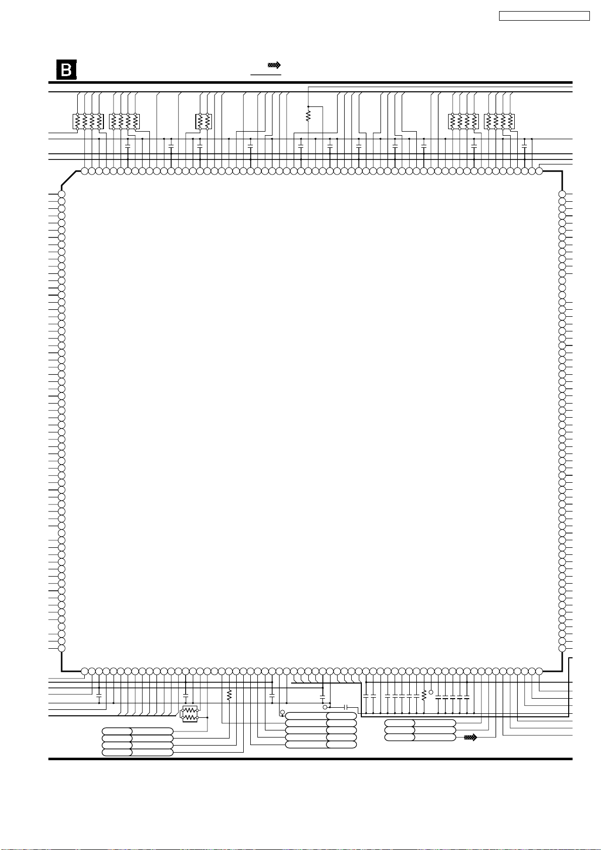
SA-VK61DGC / SA-VK61DGCS
SCHEMATIC DIAGRAM - 6
DVD MODULE 2 (DV1) CIRCUIT
MDQ(6)
MDQ(8)
MDQ(7)
MDQ(9)
MDQ(5)
MDQ(11)
RA3003
(82 x 4)
256
VDD33
1
MDQ11
2
3
MDQ3
4
VSS
MDQ12
5
MDQ2
6
VDD33
7
MDQ13
8
MDQ1
9
MDQ14
10
VSS
11
MDQ0
12
MDQ15
13
VDD33
14
VDD15
15
VSS
16
17
EXADR20
NEXWE
18
EXADT10
19
EXADT4
20
EXADT8
21
EXADT12
22
23
VDD33
VSS
24
EXADR16
25
EXADR18
26
EXADT14
27
EXADT10
28
29
VDD33
30
VSS
EXADT6
31
EXADT2
32
NEXCE
33
EXADT1
34
EXADT5
35
EXADT9
36
EXADT13
37
EXADT17
38
EXADT19
39
EXADT15
40
EXADT11
41
VDD33
42
VSS
43
EXADT7
44
EXADT3
45
NEXOE
46
P15
47
P14
48
P13
49
50
P12
51
P11
P10
52
P9
53
P8
54
P7
55
56
VDD33
MMOD
57
VSS
58
59
P6
60
P5
P4
61
62
P3
P2
63
P1
64
65 66 67 68 69 70 71 72 73
MDQ(4)
MDQ(10)
254
255
MDQ4
MDQ10
P0FGVDD15
VSS
253
MDQ5
NRST
C3029
MDQ9
VSS
MDQ6
DRV0
DQM(1)
RA3004
(82 x 4)
0.1
VSS3
MDQ8
DRV1
DRV2
0.1
C3028
248249250251252
247
246
244
245
VSS
VSS
MDQ7
DQM1
VDD15
DRV3
DRV4
DRV5
DRV6
DRV7
74
75
76
77
DQM(0)
RA3005
(22 x 2)
24379242
DQM0
DRV8
78
C3027
241
NCAS
VDD33
80
0.1
24082239
VSS
VSS
81
XCAS
VDD33
SCLOCK
XRAS
XCSM
238
NRAS
EXTRG0
83
BA1
237
NCSM
SDATA
84
236
235
BA1
VSS
EXTRG1
TRCCLK
85
86
BA0
C3026
2348823389232
BA0
MA9
TRCDATA0
TRCDATA1
87
XWE
0.1
VDD33
TRCDATA2
: CD-DA SIGNAL LINE
: +B SIGNAL LINE
MA(8)
MA(9)
MA(11)
MA(10)
R3001
0.1
C3025
231912309222993228942279522696225
VSS
MA8
MA11
MA10
MN2DS0002AP1
OSCI
VSS
VDD33
TRCST
MA7
AV DECODER
MONI7
NWE
TRCDATA3
90
J0JCC0000119
2249822399222
MCK
VDD33
IC3001
MONI6
MONI5
97
C3024
VSS
MONI4
0.1
MCKI
VDD15
MA(7)
221
VSS
VDD15
VSS
MONI3
100
MA(0)
220
101
MA(6)
C3023
219
MA0
MA6
MONI2
MONI1
102
MA(1)
0.1
218
MONI0
103
217
VDD33
104
216
MA1
AVDDD
105
MA(5)
215
MA5
PLFIL1
106
214
VSS
AVSSD
107
MA(2)
C3022
MA2
PLFIL2
MA(4)
0.1
213
108
MA(3)
212
VDD15
VREFA
109
211
MA4
VREFB
110
C3021
210
VSS
MA3
VCO
VREFC
111
0.1
209
112
DQM(2)
208
DQM2
VDD33
RESI
113
DQM(3)
RA3009
207
206
DQM3
ANAMONI
PDFLT
114
115
MDQ(16)
(82 x 4)
205
VSS
CDATA
116
MDQ(31)
204
MDQ16
MDQ31
CCAPA
117
MDQ(17)
C3020
203
MDQ17
CGD
AVDDC
118
MDQ(30)
0.1
202
201
VDD33
AVSSC
119
120
MDQ(18)
200
MDQ30
MDQ18
RFINP
RFINN
121
MDQ(19)
MDQ(29)
199
198
MDQ29
VIN5
122
123
MDQ(28)
197
VSS
MDQ19
VIN6
VIN7
124
RA3010
(82 x 4)
330
C3019
196
195
MDQ28
VIN8
125
126
194
VDD33
VIN1
127
193
VSS
MDQ20
MDQ27
MDQ21
MDQ26
VDD33
MDQ25
MDQ22
VDD15
MDQ23
MDQ24
VDD33
IECOUNT
ADOUT0
ADOUT1
ADOUT2
ADOUT3
SRCK
LRCK
PHCOPMD
EXTCK
VDD33
BECLK
COMP2
AVSSG
IREF2
AVDDG
DAC5OUT
DAC4OUT
VREF
DAC3OUT
DAC2OUT
AVSSF
DAC1OUT
AVDDF
COMP1
AVSSE
JREF1
AVDDE
DAC0
AVSSA
DAC1
AVDDA
AVDDB
VCOF
CWBLIN
CWBLOUT
CSLFLT
CTKC
AVSSB
VHALF
VREFH
LPCO1
LPC2
LPCO2
LPC1
VIN10
VIN2
VIN3
128
VSS
VSS
VSS
AD0
AD1
AD2
VIN9
VIN4
192
191
190
189
188
187
186
185
184
183
182
181
180
179
178
177
176
175
174
173
172
171
170
169
168
167
166
165
164
163
162
161
160
159
158
157
156
155
154
153
152
151
150
149
148
147
146
145
RVI
144
143
142
141
140
139
138
137
136
135
134
133
132
131
130
129
0.1
C3011
TRSDRV
SPDRV
M9V_CTL
HFMON
HIND EXTRG0
HIND TRCCLK
HIND TRCDATA (0)
TRCDATA (1)
HIND
MUTE3
FG1
SW
GAINH/L
MUTE12
RA3025
(4.7K x 2)
0.1
C3012
0
R3013
0.1
C3013
C3014
0.1
TL3012
CP3003
CLK33M AD
EXTRG1 FORE
TRCDATA (2) HIND
TRCDATA (3) HIND
TRCST HIND
73
C3031
0.1
C2051 0.033
C2003 0.1
C2054 0.1
C2053 0.1
C2052 33P
FORE
FORE
C2056 0.01
C2055 0.1
R2051 3.9K
CP3013
C2057 180P
RFINN
RFINPFORE
VIN5
C2058 0.018
C2060 0.1
C2059 5600P
C2004 0.1
Page 74

SA-VK61DGC / SA-VK61DGCS
SCHEMATIC DIAGRAM - 7
DVD MODULE 2 (DV1) CIRCUIT
C3001
C3002
6.3V330
6.3V330
RA3011
(82 x 4)
MDQ(20)
MDQ(27)
MDQ(21)
0.1
RA3012
(82 x 4)
R3041
R3043
MDQ(26)
MDQ(25)
MDQ(22)
MDQ(23)
MDQ(24)
100
100
RA3042
(100 x 2)
EXTCLK AD
CLK54M/(27M) AD
C3033
0.1
R3103
R3102
20K
2.7K
C3016
C3015
C3106
10
C3018
0.1
C3017
0.1
0.1
0.1
CP3014
C3104
LB3001
J0JHC00000045
LB3002
J0JHC00000045
C3041
22P
R3104
2.2K
: DVD (AUDIO) SIGNAL LINE: CD-DA SIGNAL LINE
: +B SIGNAL LINE : DVD (VIDEO) SIGNAL LINE
L3101
G1C100K00020
D+3.3V FORE/HIND
D+1.5V HIND
C3101 6.3V330
AUDIODIGITAL HIND
DMIXOUT AD
SRCK AD
LRCK AD
R3116
62
R3117
15
R3111
62
R3112
15
K3116
K3111
0
0
C HIND
Y HIND
C3105
10
C2006
C2005
C2035
220P
CP2032
C2033
0.1
0.1
C3103
0.1
C3102
0.1
R2033
15K
CP2033
C20321C2031
1
C3032
0.1
C2036
0.1
R3101
15K
C2037
0.01
R2032
1K
1
VIN4 FORE
VIN3 FORE
VIN2 FORE
VIN1 FORE
VIN8 FORE
VIN7 FORE
VIN6 FORE
C3107
0.1
DAC0 FORE
DAC1 FORE
AD0 FORE
AD1 FORE
AD2 FORE
CP2031
C2001
6.3V100
R2031
68K
C2034
0.015
R3105
1.5K
L2002
G1C100K00020
L2001
G1C100K00020
C2002
6.3V100
VGND HIND
VHALF FORE
VREFH FORE
LPCO1 FORE
LPC2 FORE
LPCO2 FORE
LPC1 FORE
VIN10 FORE
VIN9 FORE
D+3.3V FORE/HIND
AGND FORE/HIND
R3131
56
R3126
56
R3121
100
R3122
16
MONI (0) HIND
MONI (1)
MONI (2)
MONI (3)
MONI (4)
MONI (5)
MONI (6)
MONI (7)
HIND
HIND
HIND
HIND
HIND
HIND
HIND
K3131
0
K3126
0
K3121
0
CR/PR/R HIND
CB/PB/B HIND
Y/PY/G HIND
74
Page 75

SCHEMATIC DIAGRAM - 8
SA-VK61DGC / SA-VK61DGCS
DVD MODULE 2 (DV1) CIRCUIT
C3051
MDQ(0)
MDQ(1)
MDQ(2)
MDQ(3)
MDQ(4)
MDQ(5)
MDQ(6)
MDQ(7)
DQM(0)
XWE
XCAS
XRAS
XCSM
MA(11)
BA0
BA1
MA(10)
MA(0)
MA(1)
MA(2)
DQM(2)
MDQ(16)
MDQ(17)
MDQ(18)
MDQ(19)
MDQ(20)
MDQ(21)
MDQ(22)
MDQ(23)
0.1
C3052
0.1
C3053
0.1
C3054
0.1
C3055
0.1
C3056
0.1
C3057
0.1
C3058
0.1
10
11
12
13
14
15
16
17
18
19
20
21
22
24
25
26
27
28
29
30
32
33
34
35
36
38
39
40
41
43
1
2
3
4
5
6
7
8
9
23
31
37
42
VCC
DCQ
VCCQ
DQ1
DQ2
VSSQ
DQ3
DQ4
VCCQ
DQ5
DQ6
VSSQ
DQ7
NC
VCC
DMQ0
WE
CAS
RAS
CS
NC
BS0
BS1
A10/AP
A0
A1
A2
DQM2
VCC
NC
DQ16
VSSQ
DQ17
DQ18
VCCQ
DQ19
DQ20
VSSQ
DQ21
DQ22
VCCQ
DQ23
VCC
IC3051
VSS
DQ15
VSSQ
DQ14
DQ13
VCCQ
DQ12
DQ11
VSSQ
DQ10
DQ9
VCCQ
DQ8
VSS
DQM1
CLK
CKE
DQM3
VSS
DQ31
VCCQ
DQ30
DQ29
VSSQ
DQ28
DQ27
VCCQ
DQ26
DQ25
VSSQ
DQ24
VSS
84
81
79
75
NC
72
71
70
NC
NC
69
68
67
66
A9
65
A8
A7
64
A6
A5
A4
61
60
A3
58
NC
57
56
55
54
52
51
50
49
47
46
45
44
: +B SIGNAL LINE
86
85
83
82
C3062
0.1
80
78
77
76
C3061
0.1
74
73
63
62
59
C3060
0.1
53
C3059
0.1
48
MDQ(15)
MDQ(14)
MDQ(13)
MDQ(12)
MDQ(11)
MDQ(10)
MDQ(9)
MDQ(8)
DQM(1)
MA(9)
MA(8)
MA(7)
MA(6)
MA(5)
MA(4)
MA(3)
DQM(3)
MDQ(31)
MDQ(30)
MDQ(29)
MDQ(28)
MDQ(27)
MDQ(26)
MDQ(25)
MDQ(24)
IC3051
C3ABPJ000017
64M SDRAM
75
Page 76

SA-VK61DGC / SA-VK61DGCS
SCHEMATIC DIAGRAM - 9
DVD MODULE 2 (HIND) CIRCUIT
DV1 EXDAT (15)
DV1 EXDAT (14)
DV1 EXDAT (13)
DV1 EXDAT (12)
DV1 EXDAT (11)
DV1 EXDAT (10)
DV1 EXDAT (9)
DV1 EXDAT (8)
DV1 EXDAR (19)
DV1 EXDAR (20)
DV1 NEXWE
DV1 P (15)
DV1 EXDAR (18)
DV1 EXDAR (17)
DV1 EXDAT (7)
DV1 EXDAT (6)
DV1 EXDAT (5)
DV1 EXDAT (4)
DV1 EXDAT (3)
DV1 EXDAT (2)
DV1 EXDAT (1)
CP6316
CP6315
CP6314
CP6313
CP6312
CP6311
CP6310
CP6321
CP6322
CP6324
CP6323
CP6320
CP6319
CP6309
CP6308
CP6307
CP6306
CP6305
CP6303
CP6302
K6301
K6302
0
0
IC6301
RFKFMV71W160
16M FLASH
A15
1
A14
2
A13
3
A12
4
A11
5
6
A10
A9
7
A8
8
A19
9
A20
10
XWE
11
XRESET
12
NC
13
WP/ACC
14
RDY/XSBY
15
NC
16
A17
17
A7
18
A6
19
A5
20
A4
21
A3
22
A2
23
24
A1 A0
DQ15/A-1
IC6301
XBYTE
VSS
DQ7
DQ14
DQ6
DQ13
DQ5
DQ12
DQ4
VDD
DQ11
DQ3
DQ10
DQ2
DQ9
DQ1
DQ8
DQ0
XOE
VSS
XCE
A16
48
47
46
45
44
43
42
41
40
39
38
37
36
35
34
33
32
31
30
29
28
27
26
25
: +B SIGNAL LINE
CP6318CP6317
CP6335
CP3005
CP6334
C6302
0.1
CP3006
CP6333
CP3007
CP6332
CP3008
CP6331
CP3009
CP6330
CP3010
C6301
0.1
CP6329
CP3011
CP6328
CP3012
CP6326
CP6325
CP6301
EXADR (16) DV1
EXTRG0 DV1
MONI (7) DV1
EXTRG1 DV1
MONI (6) DV1
TRCCLK DV1
MONI (5) DV1
TRCDATA (0) DV1
MONI (4) DV1
TRCDATA (1) DV1
MONI (3) DV1
TRCDATA (2) DV1
MONI (2) DV1
TRCDATA (3) DV1
MONI (1) DV1
TRCST DV1
MONI (0) DV1
NEXOE DV1
NEXCE DV1
EXDAT (0) DV1
LB6301
J0JHC0000045
DV1
DV1
SCL
SDA
CP6351
CP6352
RA6351
(4.7K x 2)
R6351
IC6351
C3EBGZ000001
EEPROM IC
(NOT SUPPLIED)
8
C6351
0.1
100
SDA
7
SCL
IC6351
WP
6
VCC
5
GND
1
A2
2
A1
3
4
A0
76
Page 77

SCHEMATIC DIAGRAM - 10
SA-VK61DGC / SA-VK61DGCS
DVD MODULE 2 (HIND) CIRCUIT
DV1/FORE D+3.3V
C62521C6253
RA6261
DV1 DSPLCLK_DV1
CP6262
DV1 STATUS_DV1
(10K x 2)
CP6263
R6261
10K
0.01
IC6251
C0CBCBE00003
REGULATOR
OUT IN
5
1
C0JBAA000001
2
3
C0JBAA000001
2
3
IC6261
GND
INVERTER
IC6262
GND
GND
2
IC6261
INVERTER
IC6262
VCC
VCC
VCC
: +B SIGNAL LINE
4
3
51
C6261
0.1
4
51
C6262
0.1
4
LB6261
J0JBC0000015
C6251
0.1
LB3201
D0GB101JA002
LB3202
D0GB101JA002
DSPCLK-MINI AD
STATUS-MINI AD
DV1 CMD
CP6261
LB3203
D0GB101JA002
CMD-MINI AD
77
Page 78
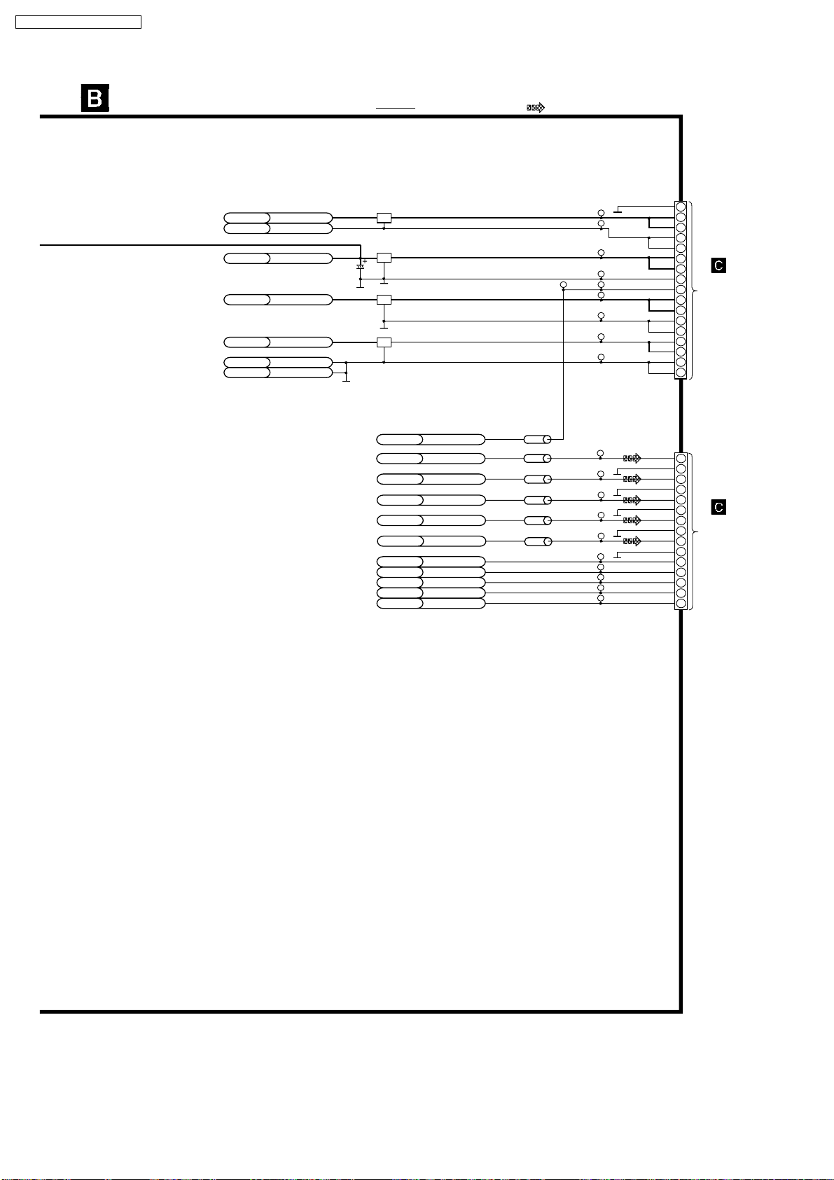
SA-VK61DGC / SA-VK61DGCS
SCHEMATIC DIAGRAM - 11
DVD MODULE 2 (HIND) CIRCUIT
FORE M+9V
FORE MGND
FORE D+5V
DV1 D+1.5V
FORE A+5V
DV1/FORE AGND
DV1 VGND
C6255
6.3V100
FL6251
F1J1E1040022
FL6252
F1H0J1050018
FL6253
F1H0J1050018
FL6254
F1H0J1050018
DV1 M9V_CTRL
DV1 Y
DV1 C
DV1 CR/PR/R
DV1 CB/PB/B
DV1 Y/PY/G
FORE TRAYREF
FORE TRAYDRV
FORE MUTE4
FORE TRV-SW+
FORE TRAY/TRV
: +B SIGNAL LINE
LB3209
D0GB101JA002
LB3204
LB3205
LB3208
LB3207
LB3206
LB3204 - 3208
J0JCC0000119
: DVD (VIDEO) SIGNAL LINE
TP6272
TP6273
TP6274
TP6275
TP6280TP6253
TP6276
TP6277
TP6278
TP6279
TP3271
TC3273
TC3274
TC3275
TC3276
TP3278
TP3279
TP3280
TP3281
TP3282
D+1.5V
D+1.5V
CR/PR/R
CB/PB/B
Y/PY/G
TRAYREF
TRAYDRV
TRAYMUT
TRV-SW+
TRAY/TRV
DGND
M+9V
M+9V
MGND
MGND
D+5V
D+5V
DGND
DGND
DGND
DGND
A+5V
A+5V
AGND
AGND
VGND
VGND
VGND
VGND
DGND
1
2
3
4
5
6
7
8
9
10
11
12
13
14
15
16
17
FP3202
Y
1
2
C
3
4
5
6
7
8
9
10
11
12
13
14
15
FP3203
TO
MAIN CIRCUIT
(CN306) ON
SCHEMATIC
DIAGRAM - 18
TO
MAIN CIRCUIT
(CN304) ON
SCHEMATIC
DIAGRAM - 18
78
Page 79

SCHEMATIC DIAGRAM - 12
SA-VK61DGC / SA-VK61DGCS
DVD MODULE (2) (AUDIO DAC) CIRCUIT
DV1 DMIXOUT
DV1 SBO1
DV1 SBT1
DV1 STBDAC
DV1 SRCK
DV1 LRCK
C4209
L4211
G1C220KA0038
LB4200
J0JBC0000015
C4210
0.1
C4212
0.1
0.1
C4203
0.1
C4202
10V10
IC4201
C0FBBK000035
2CH D/A CONVERTER
BCK
1
2
DATA
3
LRCK
DGND
4
IC4201
5
6
7
8
VDD
VCC
VOUTL
VOUTR
ZEROL
ZEROR
VCOM
AGND
: +B SIGNAL LINE
R4201
47
SCK
16
ML
15
MC
14
MDI
13
12
11
10
C4206
6.3V33
9
C4208
0.1
: MAIN SIGNAL LINE
DV1
CLK27M
G1C220KA0038
C6568
15P
L6561
C6561
6.3V33
TP6561
27MHz
L6562
G1C220KA0038
C6565
15P
LB6561
J0JBC0000015
LB6562
J0JCC0000167
C6562
6.3V33
X6501
H0J368600003
R6562
C6566
15P
C6563
0.1
C6564
0.1
220
VDD1
1
2
VSS1
3
CLK54
4
CLK27
IC6561
VDD2
5
6
VSS2
XTI
7
XTO
8
IC6561
C1DB00000980
CLOCK GENERATOR IC
CLK33
FSEL
CLK16
VDD3
VSS3
768fs
384fs
CE
16
15
14
13
12
11
10
9
C4201
6.3V100
LB6564
J0JCC0000077
C6567
0.1
R6563
10K
R6565
47
J0JCC0000119
R6564
10
LB6566
J0JBC0000015
LB6567
TP6563
33.8MHz
TP6564
16.9MHz
TP6565
EXTCLK
DV1CLK33M
DV1CLKSEL
DV1
79
Page 80
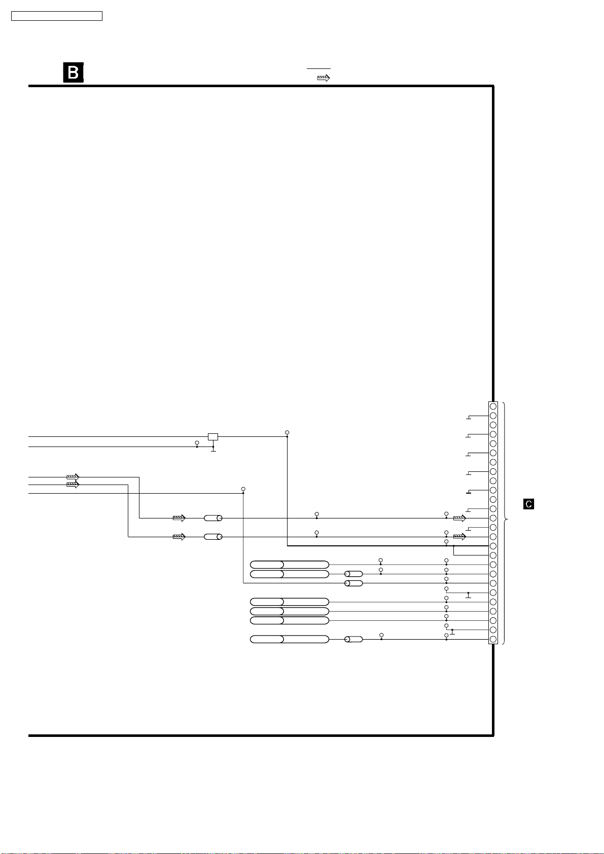
SA-VK61DGC / SA-VK61DGCS
SCHEMATIC DIAGRAM - 13
DVD MODULE (2) (AUDIO DAC) CIRCUIT
: +B SIGNAL LINE
: MAIN SIGNAL LINE
TC4215
FL4201
F1H0J1050018
LB4215
J0JCC0000119
LB4214
J0JCC0000119
TC4220
DV1 25BSY (AC3H)
DV1 AMUT
HIND CMD-MINI
HIND STATUS-MINI
HIND DSPCLK-MINI
DV1
TC4218
AUDIODIGITAL
TC4217
TC4216
LB4216
LB4217
LB4201
J0JCC0000119
TC4214
TC4219
LB4216, 4217
J0JBC0000015
TC4201
TC4278
TC4279
TC4280
TC4281
TC4282
TC4283
TC4284
TC4285
TC4286
TC4287
TC4288
TC4289
AGND
CNT
AGND
AGND
AGND
AGND
AGND
MIXR
AGND
MIXL
ADAC5V
ADAC5V
AC3H/DACMUT
AMUT
ZFLAG
DGND
CMD
STATUS
DSPCLK
DGND
AUDIODIGITAL
SW
SR
SL
FR
FL
FP4202
1
2
3
4
5
6
7
8
9
10
11
12
13
14
15
16
17
18
19
20
21
22
23
24
25
26
TO
MAIN CIRCUIT
(CN303) ON
SCHEMATIC
DIAGRAM - 16
80
Page 81
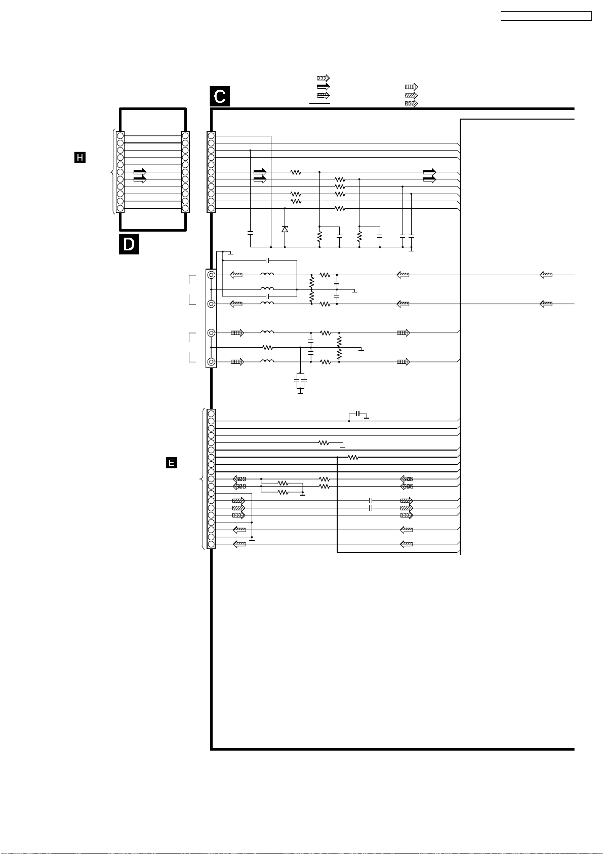
20.3. (C) Main Circuit & (D) Tuner Extent Circuit
SA-VK61DGC / SA-VK61DGCS
SCHEMATIC DIAGRAM - 14
TO
TUNER CIRCUIT
(CP100) ON
SCHEMATIC
DIAGRAM - 31
11
10
9
8
7
6
5
4
3
2
1
TUNER
EXTENT
CIRCUIT
11
10
9
8
7
6
5
4
3
2
1
LINE OUT
AUX
R
R
JK304
11
10
L
L
MAIN CIRCUIT
TUNER_GND
+15V
TUNER_SD
9
TUNER_DO/ST
8
RDS_DETECT
7
TUNER_RCH
6
TUNER_LCH
5
TUNER_DI
4
TUNER_CLK
3
TUNER_CE
2
+7.5V
1
CN307CP703CP702
C704
0.01
C347 0.22
L67
J0JBC0000041
L60
J0JBC0000019
C343 0.22
L66
J0JBC0000041
L64
J0JBC0000041
R385
2.2
L65
J0JBC0000041
R213 0
R701 4.7K
D301
B0BC5R000009
C359
0.22
R401
47K
R201
47K
R216
47K
C364
0.22
C402
1000P
C202
1000P
R413 0
R742 0
R744 0R743 0
R702 27
C207
3300P
R402
10
R202
10
R403
10K
R203
10K
: MIC SIGNAL LINE
: AM/FM SIGNAL LINE
: MAIN SIGNAL LINE
: +B SIGNAL LINE
C407
R416
3300P
1000P
C401
1000P
C201
1000P
R404
5.6K
R204
5.6K
47K
C413
: AUX SIGNAL LINE
: PLAYBACK SIGNAL LINE
: RECORD SIGNAL LINE
+15V
SD
PLLD_IF
TUN_R
TUN_L
PLLDA
SERB
PLLCE
+9V
C412
1000P
AUX_L
AUX_R
TO
PANEL CIRCUIT
(CP601) ON
SCHEMATIC
DIAGRAM - 29
CN601
19
18
17
16
15
14
13
12
11
10
9
8
7
6
5
4
3
2
1
SPEA
+9V
NJULAT
PGND
VREF+
LED9V
MUTEA
+15V
REC_R
REC_L
AGND
PBR
PBL
MIC
MICGND
HPR
HPGND
HPL
R206 470
R406 470
W5
R205
47K
R405
47K
C345
560P
0
W6
0
C216 1
C416 1
SPEA
NJU_LAT
VREF+
LD9V
MUTEA
+15V
DSP_RIN
DSP_LIN
PBR
HPR
LED9V
+9V
PBL
MIC
HPL
81
Page 82

SA-VK61DGC / SA-VK61DGCS
SCHEMATIC DIAGRAM - 15
MAIN CIRCUIT
C203
50V4.7
C403
-9V
MUTE_L
SPEA
KA_LOUT
KA_ROUT
+9V
KA_LIN
SERE
SERF
NJU_LAT
PBL
AUX_L
TUN_L
MIXL
DSP_LIN
R266
330K
W3
0
50V4.7
R314
0
R466
330K
R473
R419
100K
10K
IC301
C0JZAS000004
ANALOG SWITCH IC
: -B SIGNAL LINE
: +B SIGNAL LINE
R209
0
R409
0
B1GDCFGA0014
MUTING SWITCH
C339
47P
C340
47P
C341
47P
W40
W2
Q301
Q301
0
0
R301
27K
CK
IC301
C301
50V4.7
171516
DATA
Q300
R303
1K
R304
56K
W27
0
NC
: AUX SIGNAL LINE
: PLAYBACK SIGNAL LINE
: RECORD SIGNAL LINE
Q300
B1GFGCAA0001
MUTING CONTROL
654
123
R302
1K
R414
10K
C435
50V4.7
R472
100K
S7
S8
C3
: MAIN SIGNAL LINE
: AM/FM SIGNAL LINE
C205
R211
50V3.3
1K
R210
100K
R410
100K
R411
1K
C405
50V3.3
C303
0.01
C410
100P
C411
470P
R412
2.7K
S5
S6
C2
C1
KIA4558FEL
DUAL OP-AMP
5
6
IC302
7
8
R470
100K
C409
16V10
C414
100P
R415
100K
S3
S4
IC302
R476
47K
S2
R270
100K
C304
0.01
C209
16V10
29 30
S1
4
3
C210
100P
2
C211
470P
1
R212
2.7K
C307
0.01
VDD
C214
100P
R215
100K
R214
10K
C235
50V4.7
DSP_RIN
MIXR
TUN_R
AUX_R
PBR
KA_RIN
-9V
R219
10K
VSSSTNC
82
VEE
C334 0.01
12
328427526625724823922102111201219131814
R276
47K
R272
100K
Page 83
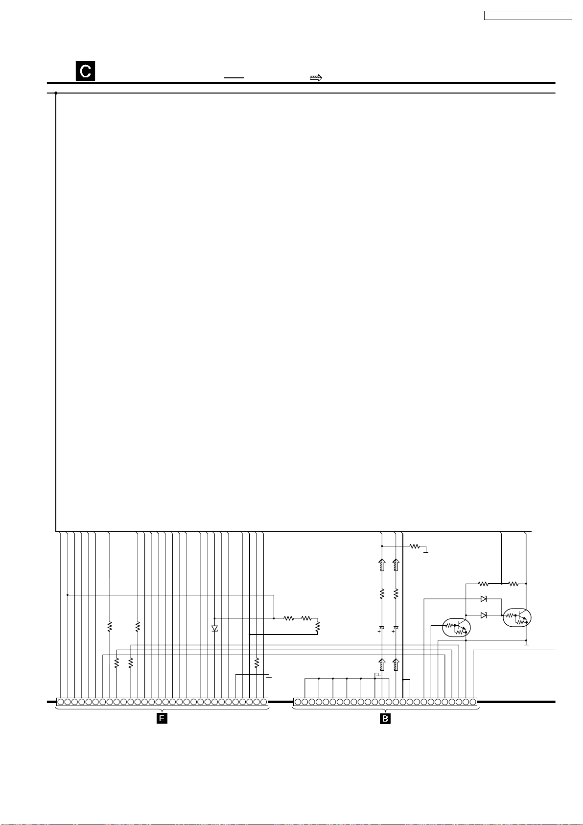
SCHEMATIC DIAGRAM - 16
SA-VK61DGC / SA-VK61DGCS
MAIN CIRCUIT
: +B SIGNAL LINE : MAIN SIGNAL LINE
SERE
DSP_RST/
SERE
DSP/RST
2
1
VOL_CS
DSP_CS
VOL_CS
DSP_CS
4
3
SERF
SERF
5
PLLCE
W30
PLLCE
6
SERB
PLLDA
W23
0
0
0
0
W10
W11
DVDCMD
PLLDA
DVDSTA
SERC
DVDCLK
SERB
8
10
12
9
11
7
TO
PANEL CIRCUIT
(CP602) ON
SCHEMATIC DIAGRAM - 29
CHG_HALF
DVD_MUTE
CHG_HALF
DVD_MUTE
13
14
SERA
CHG_CW
CHG_CW
SERA
16
15
PLLD_IF
CHG_CCW
CHG_PLGR
CHG_CCW
PLLD_IF
CHG_PLGR
18
19
17
DCDET
DSP_DO
DCDET
21
20
SD
SERD
KARA_LA/REGIN
D22
B0ACCK000005
SERD
KEYLATSDCHG_AD1
22
23
24
CHG_AD1
DGND
25
26
SW5V
CHG_AD2
W9
CHG_AD2
SW5V
28
27
R273
100K
MIXL
AV5V
MOT10V
CHG_SW
W16
W14
0
0
R317
5.6K
0
CHG_SW
29
MOT10V
30
SW
AGND
AGND
AGND
CENTERSRSL
2
3
1
CN602 CN303
AGND
8
4
6
5
7
MIXR
R422 8.2K
R222 8.2K
C219 16V10
C419 16V10
AGND
AGND
AGND
AV5V
13
MIXR
AV5V
MIXL
AC3H/DACMUT
18
16
14
15
17
FR
FL
10
12
9
11
TO
DVD MODULE 2 CIRCUIT
(FP4202) ON
SCHEMATIC DIAGRAM - 13
AMUTE
19
ZFLAG
20
21
SUB+BGND
DVD_CMD
DVD_STA
22
23
83
B0ACCK000005
B0ACCK000005
DVDCLK
SUB+BGND
25
24
Q15
AUDIO_SIG
26
AV5V
D21
R36
10K
R35
10K
D20
Q16
Q15, Q16
B1GBCFJN0021
MUTING SWITCH
DVD_MUTE
Page 84
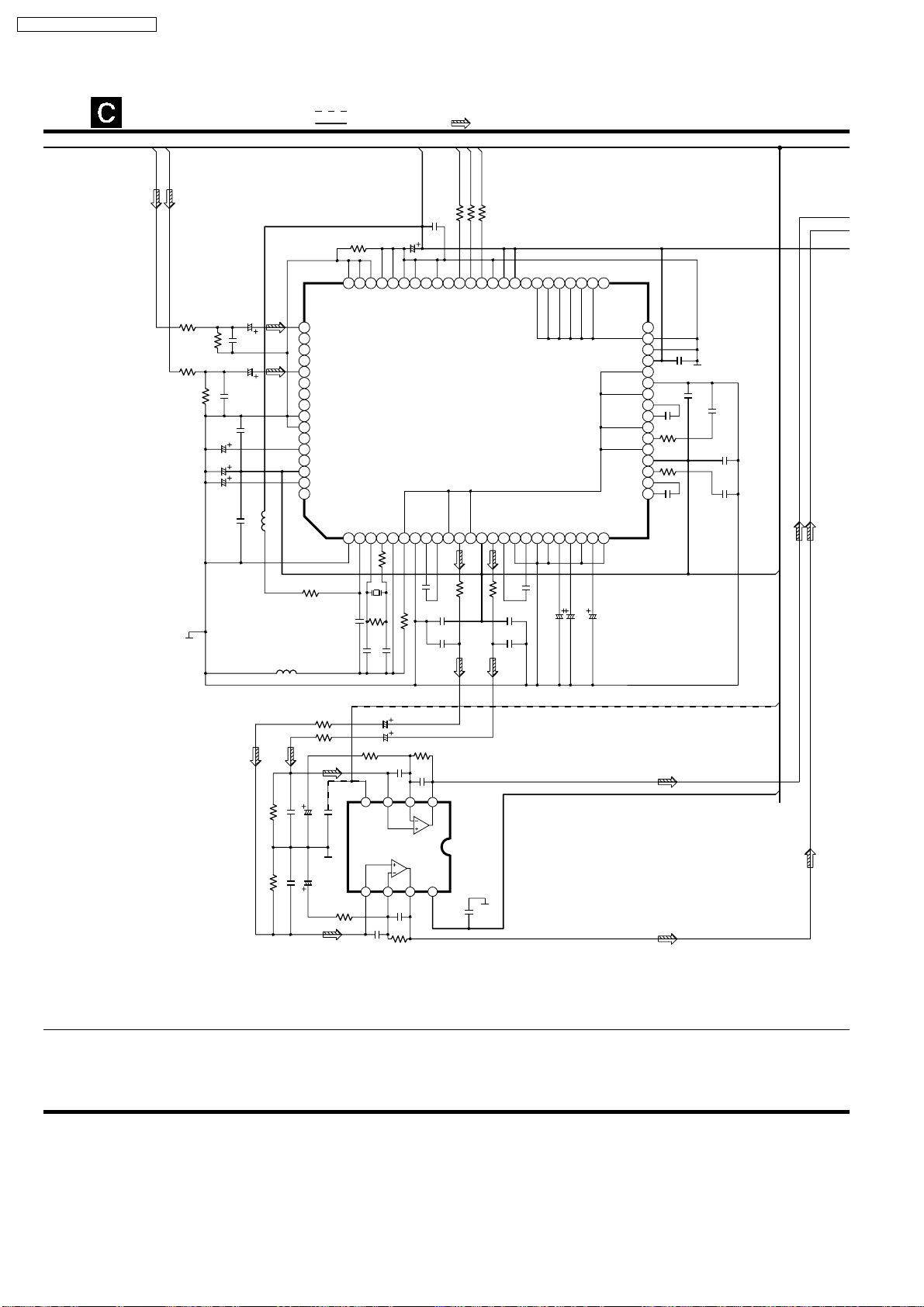
SA-VK61DGC / SA-VK61DGCS
SCHEMATIC DIAGRAM - 17
MAIN CIRCUIT
DSP_LIN
DSP_RIN
: -B SIGNAL LINE
: +B SIGNAL LINE
R725
C725
16V100
0
DSP_D+5V
C724
0.1
: MAIN SIGNAL LINE
SERF
SERE
DSP_CS
R712 330
R713 330
R711 4.7K
R463
4.7K
R263
4.7K
R268
3.3K
R468
3.3K
C705
50V4.7
C706
10V220
C707
50V4.7
C770
0.1
C264
1000P
C415
50V1
C464
1000P
C215
50V1
C765
0.1
L12
G0A100G00005
X700
H0H368600001
L13
J0JBC0000019
R434 3.9K
LIN4
65
66
LIN3
LIN2
67
LIN1
68
69
RIN4
70
RIN3
71
RIN2
72
RIN1
NC
73
74
GNDAL
OUTL
75
VRAL
76
NC
77
VDALR
78
VRAR
79
80
OUTR
R706
47
R234 3.9K
C708
0.1
64
NC
GNDAR
12
616263
60
NC
NC
TST1
TST0
VDXXIXO
GNDXNCGNDA1
4
5
3
1K
R707
X700
R708
1M
C710 12P
C709 12P
C430 50V4.7
C230 50V4.7
R236
3.9K
C233
100P
364
59
I2CS
GND
6
7
C711
W20 0
R237
33K
C234
47P
8
1
531352
54
55
565758
NC
/CS
IFDI
IFCK
/ERR
IFDO
IC700
C2HBZC000013
DSP IC
AI1
AO1NCAOT1NCVDA12
12
9
10
11
R433
270
C712
C429
2200P
12
R233
1
51
14
270
50
NC
AOT2
15
C714
C229
2200P
48
49
VDD
/RST
AO2NCAI2
16
17
C713
1
1
47
46
NC
DOUT
GNDA2NCVRD1
19
18
44
45
NC
DIN0
DIN1
VRINCVRD2
21
20
C715 16V100
41
42
43
NC
DIN2
EBCI/O
GNDA3
22
23
24
C716 16V47
C717 16V100
ELRI/O
SYNC
GNDR
VDDR
GND4
AO4
AOT4
VDA34
AOT3
AO3
40
39
38
37
NC
C722
36
0.1
35
NC
34
AI4
33
32
NC
31
30
NC
29
28
27
26
25
AI3
C721
R319
270
R320
270
C718
C720
0.1
1
1
C322
2200P
C719
0.1
C324
2200P
DSP_A+5V
-9V
+9V
C231 1000P
R235 22K
C431 1000P
R435 22K
C352 0.01
C232 16V10
R436
C432 16V10
3.9K
IC306
78
5
C433
100P
C434
47P
R437
33K
C351
0.01
IC306
KIA4558FEL
DUAL OP-AMP
84
Page 85
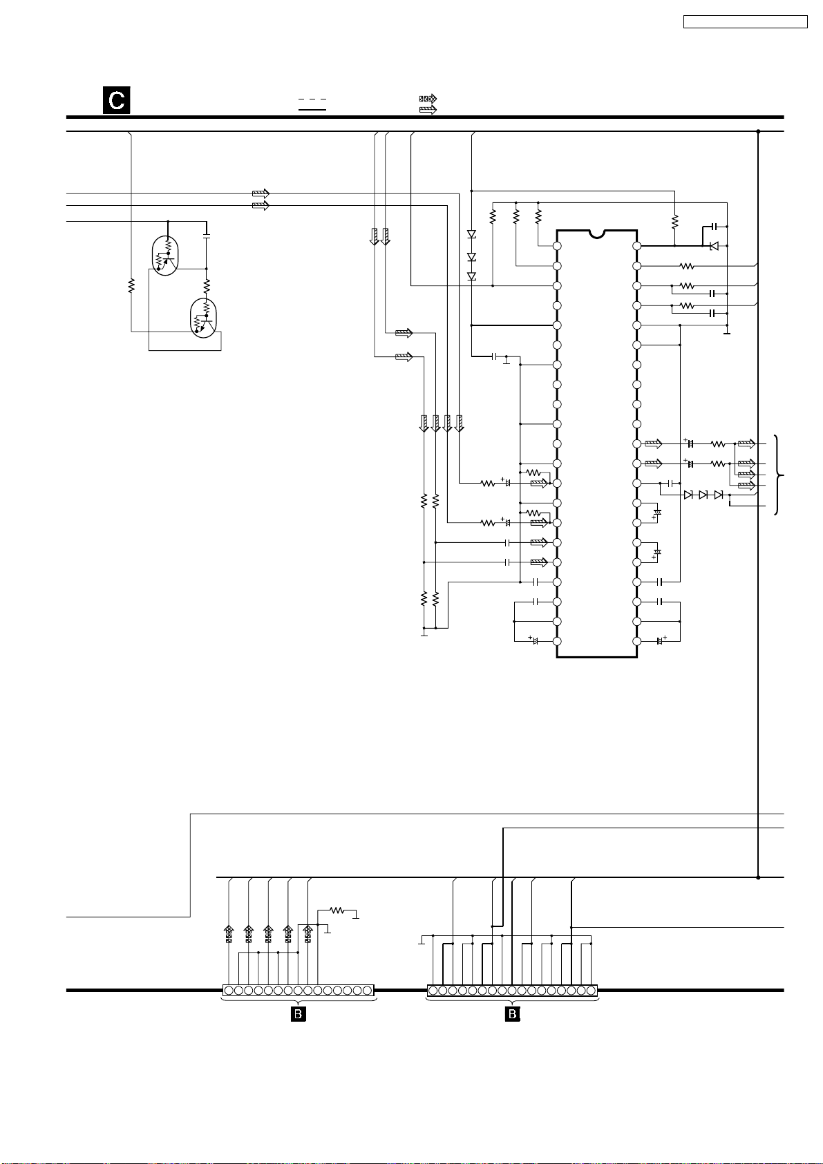
SCHEMATIC DIAGRAM - 18
MAIN CIRCUIT
: -B SIGNAL LINE
: +B SIGNAL LINE
: DVD (VIDEO) SIGNAL LINE
: MAIN SIGNAL LINE
SA-VK61DGC / SA-VK61DGCS
R710
4.7K
DSP_RST/
Q700
Q701
C764
0.1
R749
10K
Q700
B1GDCFGG0021
SWITCH
Q701
B1GBCFGG0023
SWITCH
DSP_LIN
DSP_RIN
WIDE
R427 1K
R469 22K
R227 1K
R269 22K
+9V
D312, 313, 315
B0ACCK000005
R343
47K
D312
D313
D315
C356 0.1
C260
R238
50V1
1K
C460
R438
50V1
1K
C261
1
C461
1
R344
47K
R257
R457
8200P
50V0.33
27K
27K
C437
C438
0.015
C439
R345
47K
PORT1
1
PORT2
2
PORT3
3
PORT4
4
AVDD
5
SWIN
6
7
GNDS
SRIN
8
SLIN
9
10
GNDC
CIN
11
IC307
12
GNDR
RIN
13
14
GNDL
LIN
15
16
BYPASSR
17
BYPASSL
LTRE
18
19
LBASS3
20
LBASS2
LBASS1
21
IC307
C1BB00000782
6-CHANNEL VOLUME
DVDD
CLOCK
DATA
LATCH
DGND
AGND
SWOUT
SROUT
SLOUT
COUT
ROUT
LOUT
AVSS
CR1
CR2
RTRE
RBASS3
RBASS2
RBASS1
CL1
CL2
D303
B0BC5R000009
C353
R346
0.1
390
0.1
C354 47P
C355 47P
C241
50V4.7
C441
50V4.7
D310
D314
D310, 311, 314
B0ACCK000005
D303
R241
5.6K
R441
5.6K
D311
SERF
SERE
VOL_CS
-9V
A
B
C
D
E
42
R347 4.7K
41
R348 2.2K
40
R349 2.2K
39
38
37
36
35
34
33
32
31
C357
30
29
C457
16V10
28
27
C257
16V10
26
25
C237
8200P
24
C238
0.015
23
22
C239
50V0.33
Y
C
CB/PB/B
CR/PR/R
VGND
VGND
VGND
VGNDYC
CR/PR/R
2
1
CB/PB/B
4
3
6
5
7
TO
DVD MODULE 2 CIRCUIT
(FP3203) ON
SCHEMATIC DIAGRAM - 11
8
Y/PY/G
SUB+BGND
Y/PY/G
10
9
TRAYREF
11
W18
D+1.5V
D+1.5V
SUB+BGND
12
11
A+5V
SUB+BGND
A+5V
A+5V
13
14
15
SUB+BGND
SUB+BGND
16
17
0
SUB+BGND
TRAY/TRV
TRV-SW+
TRAYMUT
TRAYDRV
12
13
14
15
CN304 CN306
1
MOT10V
2
D+5V
MOT10V
MOT10V_CTL
MOT10V
SUB+BGND
SUB+BGND
D+5V
D+5V
SUB+BGND
MOT10V_CTL
D+1.5V
8
4
3
5
TO
DVD MODULE 2 CIRCUIT
(FP3202) ON
SCHEMATIC DIAGRAM - 11
10
6
9
7
85
Page 86
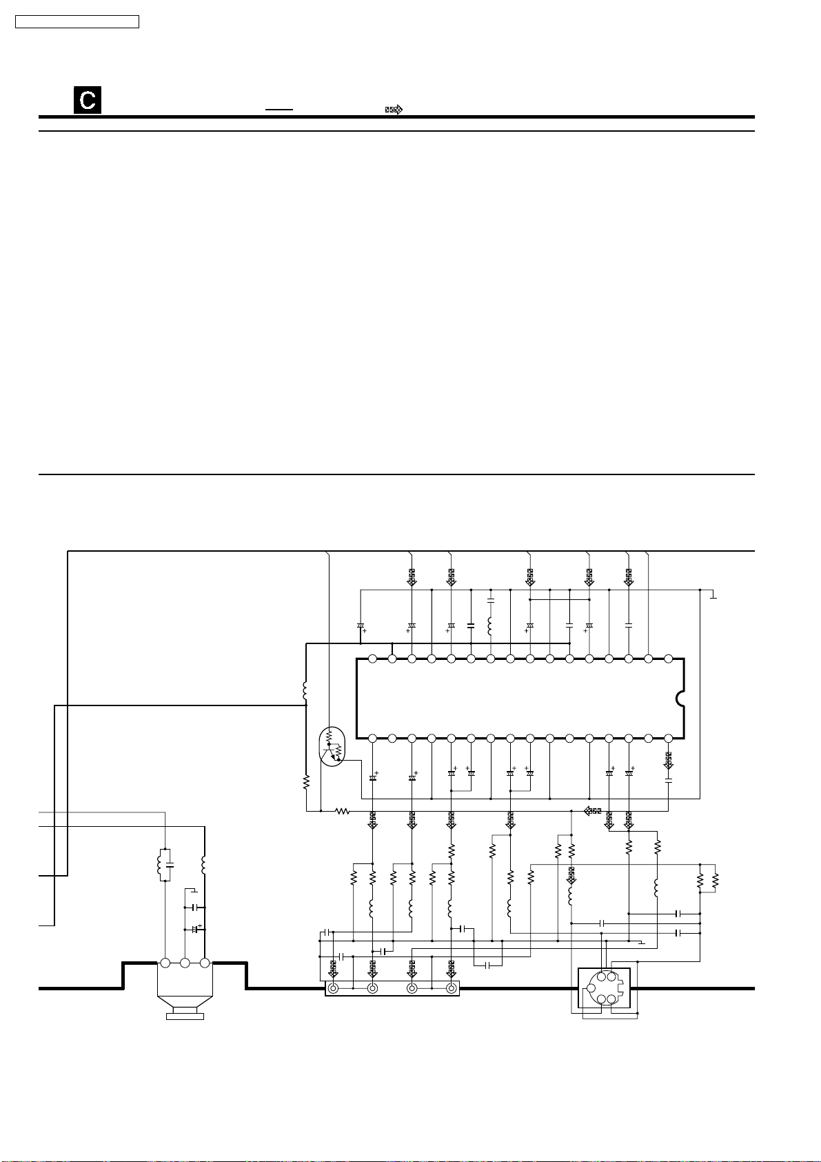
SA-VK61DGC / SA-VK61DGCS
SCHEMATIC DIAGRAM - 19
MAIN CIRCUIT
: +B SIGNAL LINE : DVD (VIDEO) SIGNAL LINE
C76
L58
0.01
J0JBC0000019
1
OUTPUT
OPTICAL
16V10
2
C75
0.01
C302
GND
L59
J0JBC0000019
3
JK305
VCC
L50
ELESN220JA
R54
2.2K
Q52
B1GBCFJN0021
INVERTER SWITCH
Q52
C77
1000P
WIDE
100K
C72
CB
R55
10K
R65
1
C50 10V220
CRFIL
CR OUT
17
C67 6.3V330
R66
R56
100K
75
L52
VLP0145-T
C78
1000P
CR
CR/PR/R
VMUTE2
CBFIL
C66 6.3V330
R57
75
L53
VLP0145-T
C51 16V47
GND
CR IN
CB OUT
GND
R67
100K
VIDEO
CB/PB/B
CB IN
PY OUT2
C65 6.3V100
R64
R58
75
L54
VLP0145-T
1000P
Y
ELJFCR39KF
C53 0.01
C52 16V47
VCC2
PY OUT1
C64 6.3V1000
R68
100K
0
C80
C79
470P
L51
Y/PY/G
22P
C54
L51
C55 16V47
GND
PY IN
PYFIL
IC50
C9ZB00000377
VIDEO BUFFER
GND
Y OUT2
Y OUT1
C62 6.3V1000
C63 6.3V100
R62
R59
0
75
L55
VLP0145-T
R69
100K
GND
GND
Y
C56 0.01
VCC1
YFIL
R60
75
L56
VLP0145-T
C57 16V47
Y IN
GND
GND
MIX OUT2
C61 6.3V100
R70
100K
C81
470P
4
Y
5
C
3
S-VIDEO
C
C58 0.01
33042952862772682592410231122122113201419151816
C IN
MIX OUT1
C60 6.3V1000
1
G
2
VMUTE
VMUTE1
TEST
31 32
R61
75
L57
VLP0145-T
JK301JK302
12
CFIL
C OUT
C59
0.01
C73
1
C82
470P
R731R74
1
86
Page 87
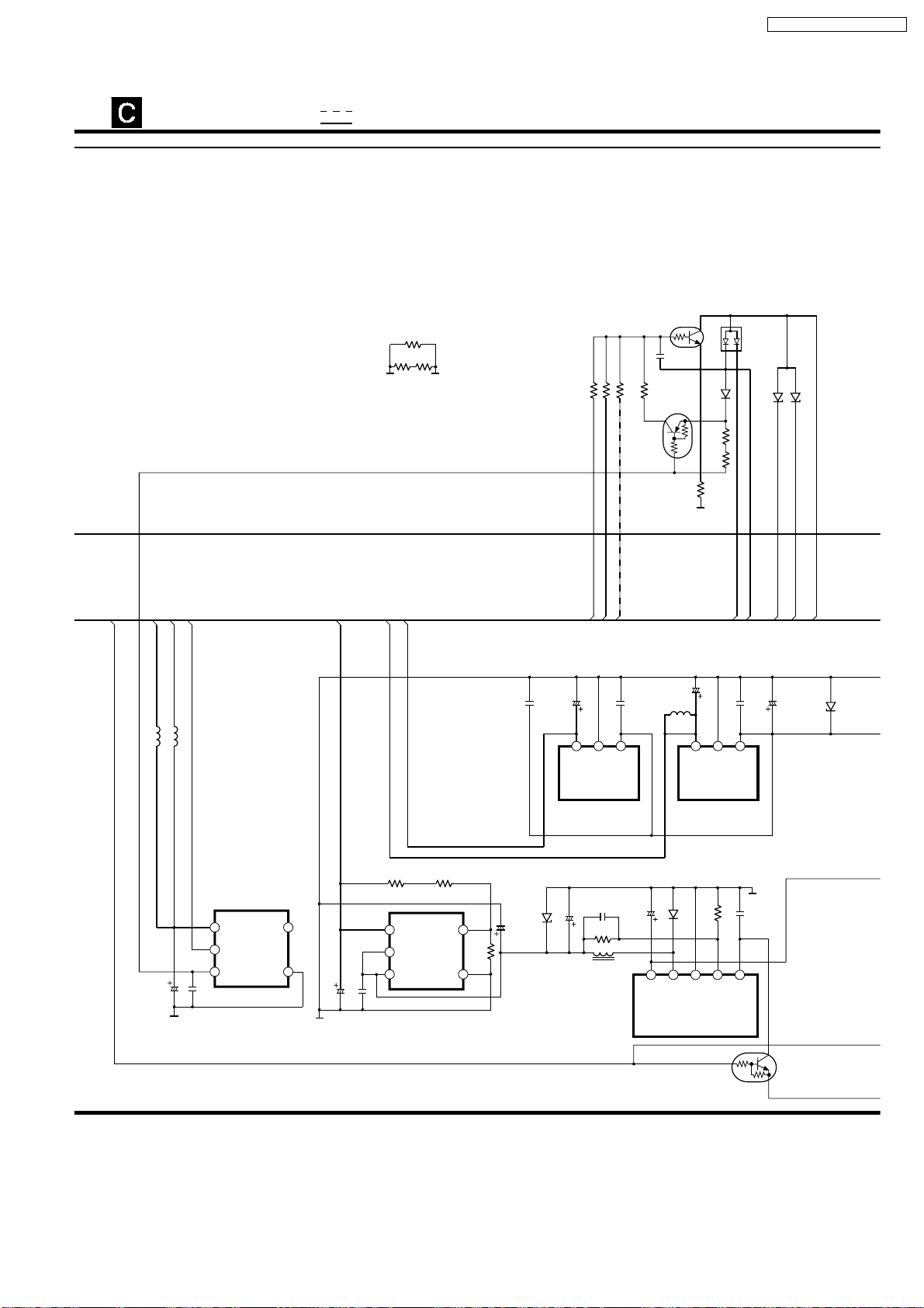
SCHEMATIC DIAGRAM - 20
MAIN CIRCUIT
: -B SIGNAL LINE
: +B SIGNAL LINE
Q801
B1GBCFJA0015
SWITCH
SA-VK61DGC / SA-VK61DGCS
DVD_PCNT
DSP_A+5V
DSP_D+5V
L11
L10
G0A100G00005
G0A100G00005
DSP_PCNT
D+1.5V
R900
R9010R902
AV5V
D+5V
0
1
R18
4.7K
C823
4.7
Q6
L8
G0A100G00005
C12
6.3V220
L8
0
R19 4.7K
R897 15K
R896 39K
Q6
B1GDCFJJ0023
SWITCH
DVD_AC
+9V
-9V
C26
C27
6.3V220
1
C25
1
23
IC6
D806
B0ADCJ000020
D10
B0EAKM000117
R21
1
R22
1
W8
0
MOT10V
LED9V
C11
1
1
23
D805
B0ACCK000005
SW5V
+9V
C7
16V10
D807
B0ACCK000005
DCDET
D9
B0BC7R500001
IC2
Q801
C21
6.3V100
3
2
IC5
1
C22
0.1
IC5
C0DBZHE00017
POWER SUPPLY IC
IC6
C0CBADG00005
5V REGULATOR
R26
270
4
5
C30
10V100
C29
3
2
1
1
C0DBCFG00004
R25
10
IC8
IC8
1.5V REGULATOR
C15
C14 1
D8
C16
6.3V820
B0BC7R500001
R24
C17
16V10
1K
4
5
R15
1K
L6
G0A101G00022
25V220
Vin
C0DBAMH00009
POWER SUPPLY IC
IC2
C0CBADG00005
5V REGULATOR
R14
1K
D7
B0JCP000004
4
21
Vout
IC3
5
3
0adj
COM
C13
Vsoft
1
Q17
B1GBCFJN0021
PCONT SWITCH
87
Page 88
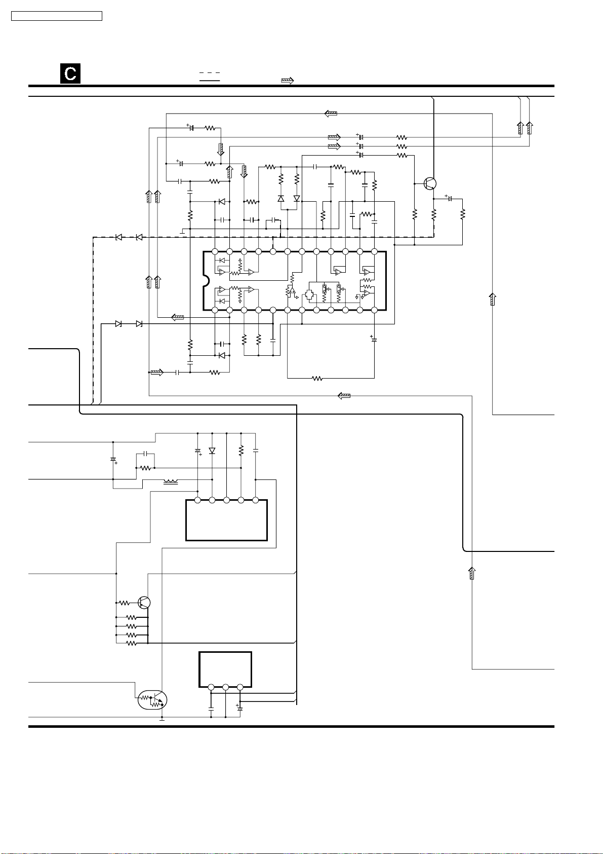
SA-VK61DGC / SA-VK61DGCS
SCHEMATIC DIAGRAM - 21
MAIN CIRCUIT
: -B SIGNAL LINE
: +B SIGNAL LINE
: MAIN SIGNAL LINE
D201
B0ACCK000005
D306 D307
D306, 307
B0BC7R5000001
D308, 309
B0ACCK000005
D308 D309
16V10
C253
0.056
C453
0.056
C263
C463
16V10
C254
0.15
R261
39K
R461
39K
C454
0.15
R459
68K
R259
68K
R260
4.7K
R460
4.7K
+9V
D700,701
B0AACK000005
R724
3.3K
R745
270
R723
D201
12K
D700
C731
C729
C255
270P
24
23
10K
22K
22K
15K
2
1
C455
270P
D401
0.01
100P
VEE
VCC
3224215206
C742 0.01
R739 100K
R740 15K
D401
B0ACCK000005
27K
R746
270
19
D701
3.3K
C733
0.1
R728
18
17
8
7
R736
15K
R729
4.7K
0.047
270K
3.9K
916101511
C734
1.8K
C456 50V4.7
C256 50V4.7
C732 16V10
R730
8.2K
C735
0.15
C736
5600P
R462 2.7K
R262 2.7K
R727 1K
Q321
B1ABCF000131
SWITCH
Q321
R731
100K
R732
100K
C737
0.047
14
13
22K
22K
12
C773
16V10
IC701
M62456FPE1
DIGITAL SOUND
CONTROLLER
R737
22K
R733
560
C741
16V10
R738
4.7K
FR_L
FR_R
+9V
-9V
6.3V820
R10 1
Q18
B1GBCFJN0021
PCONT SWITCH
C8
R6
1
R7 1
R8 1
R9 1
C10
3.9K
1
R17
Q5
Q18
G0A101G00022
C9
25V220
L9
Vin
C0DBAMH00009
POWER SUPPLY IC
Q5
B1ADCF000001
CURRENT LIMITTER
C0CBADG00005
5V REGULATOR
123
C19
1
21
Vout
R16
1K
D6
B0JCP000004
3
COM
IC4
IC9
IC9
4
0adj
10V100
C20
C18
1
5
Vsoft
DVD_AC
SUB+B
MOT10V
FAN5V
88
Page 89

SCHEMATIC DIAGRAM - 22
MAIN CIRCUIT
: -B SIGNAL LINE
: +B SIGNAL LINE
SA-VK61DGC / SA-VK61DGCS
: MAIN SIGNAL LINE
A
B
C
D
E
R243
56K
C459
25V330
321
456
C242
50V4.7
W15
0
C442
50V4.7
R245
2.7K
R445
2.7K
R265 3.3K
Q308
R465
3.3K
C376
0.01
R443
56K
C0AABB000117
Q308
B1GFGCAA0001
MUTING CONTROL
R248
27K
C246
33P
C245
100P
78
5
IC308
OP-AMP
364
C446
33P
C445
100P
R448
27K
12
R394
-9V
Q314
Q314, 317
Q317
R338
R340
0
0
MUTE_A
HP_MUTE
HPR
HPL
+9V
R361
56K
R360
56K
C362
50V22
C247
0
C377
0.01
16V47
W26
0
W22
0
C447
16V47
R249
82
R250
82
R450
82
R449
82
C248
1000P
C448
1000P
R452
R451
R252
82
R251
82
82
82
W25
R253
4.7K
0
6
5
4
R267
1K
1
R467
1K
2
3
Q312
R453
4.7K
Q312
B1GFGCAA0001
MUTING CONTROL
R367
56K
C365
50V4.7
R254 10
R454 10
B1GDCFGA0014
MUTING SWITCH
R366
56K
89
Page 90

SA-VK61DGC / SA-VK61DGCS
SCHEMATIC DIAGRAM - 23
MAIN CIRCUIT
TO
CD LOADING
CIRCUIT
(CN1) ON
SCHEMATIC
DIAGRAM - 38
CN309
CHG_CW
14
CHG_HALF
13
8V
12
CHG_CCW
11
CLAMP
10
OPEN
9
SW1
8
PGND
7
SW2
6
DGND
5
5V
4
POSITION
3
BOTTOMSW
2
PLUNGER
1
: -B SIGNAL LINE
: +B SIGNAL LINE
R108 27K
R109 12K
R104 12K
C100
0.47
R105 22K
R110 220
R111 22K
R112 12K
: MAIN SIGNAL LINE
R100 10K
R101 10K
R103
10K
Q100
KRC102MTA
PLUNGER MOTOR SUPPLY
CONTROL SWITCH
R106
1K
VREF+
CHG_CW
CHG_HALF
CHG_CCW
CHG_AD1
CHG_AD2
CHG_SW
CHG_PLGR
MOT10V_CTL
Q4
B1BBCF000006
SWITCH
LD9V
MOT10V
D100
B0EAKM000117
Q101
Q101
KTA12710YTA
CD MOTOR SUPPLY SWITCH
-9V
+8V
FAN
SW5V
+9V
DCDET
MUTE_H
FRR
FRL
R107
10K
+15V
MOT10V
+8V
SW5V
SUB+B
Q7
B1GBCFJN0021
CURRENT CONTROL
Q8
B1GDCFGA0014
CURRENT CONTROL
Q7
Q8
D12
B0JCPC000004
Q4
R72
4.7K
D11
B0BC013A0007
W39
0
R75
470
C70
16V220
MOT10V
LED9V
FAN
SW5V
+8VNCDIGITAL_GND
-9V
+9V
VIDEO_GND
DSP_GND
POWER_GND
9
12
11
CN301 CN300 CN302
10
TO
POWER SUPPLY CIRCUIT
(CP501) ON
SCHEMATIC DIAGRAM - 34
4
8
6
7
1
5
2
3
12
W38 0
W36 0
W35 0
W34 0
W32 0
W31 0
W33 0
MUTE_H
DCDET
11
TO
POWER SUPPLY CIRCUIT
(CP500) ON
SCHEMATIC DIAGRAM - 34
AGND
FRL
9
AGND
4
8
5
6
7
FRR
10
+15V
TGND
1
2
3
90
SUB+BNCSUB+BGND
1
3
2
TO
POWER CIRCUIT
(W953) ON
SCHEMATIC DIAGRAM - 36
Page 91

SCHEMATIC DIAGRAM - 24
MAIN CIRCUIT
SA-VK61DGC / SA-VK61DGCS
: MIC SIGNAL LINE
: +B SIGNAL LINE : MAIN SIGNAL LINE
SERD
SERA
DVD_PCNT
KA_ROUT
KA_LOUT
KA_RIN
KA_LIN
MIC
L700
G0C100JA0030
IC703
C1BB00000574
I/O EXPANDER
C270 16V10
C470 16V10
C769
50V1
C622
0.1
C623
1000P
C621 47P
C620 47P
R633
C768
100
50V1
SW5V
VCC
GND
1
R626
15K
DSP_PCNT
R632
4.7K
14
1516
DSP_PCNT
DAT
2
VMUTE
R631 4.7K
13512
NC
VMUTE
IC703
CLK
MUX_CTL
4
3
R625
10K
R624 4.7K
HP_MUTE
R630 1K
R629 4.7K
11
HP_MUTE
MUTE_SW
MUTE_C
MUTE_SNCDVD_PCNT
6
R622 4.7K
R623 4.7K
MUTE_L
10
MUTE_L
7
MUTE_H
R627 4.7K
R628 1K
9
MUTE_H
8
R620 4.7K
SW5V
R704
5.6K
C763
3300P
R717
15K
R714
10K
C701
4700P
C728
1000P
R715
4.7K
R716
10K
R700
15K
R703 3.9K
C727 1000P
C703 1000P
C762 50V2.2
C730
820P
C743 0.068
C744 0.068
C745 0.068
C747 16V47
C748
16V100
R718
0
C738
0.047
C746
0.047
C749
0.1
C700
50V2.2
C702
560P
R705
27K
1
2
3
4
5
6
7
8
9
10
11
12
13
14
15
16
17
18
19
20
21
22
23
24
C767 50V1
C766 0.15
R741 10K
R726 10K
IC702
C1BB00000801
KARAOKE IC
25 26 27 28 29 30 31 32 33
R719
C750
12K
0.1
R720
10
R747
220
W4 0
SERE
71
70
727374757677787980
34
35
C771 1000P
R748 220
C772
1000P
SERF
KARA_LA/REGIN
366937
68
3867396640
C751
1000P
65
C472
64
63
62
61
60
59
58
57
56
55
54
53
52
51
50
49
48
47
46
45
44
43
42
41
50V1
C272
50V1
C761
0.1
C759
50V1
C757
1000P
C756
0.068
C753
0.068
R721
C760
16V100
C758
1000P
C755
C754
C752
1000P
0
0.1
0.1
91
Page 92

SA-VK61DGC / SA-VK61DGCS
SCHEMATIC DIAGRAM - 25
MAIN CIRCUIT
: -B SIGNAL LINE
: +B SIGNAL LINE
-9V
L370
G0C221KA0007
Q374
B1ADCF000001
FAN MOTOR DRIVE
D375, 376
B0ACCK000005
B0BC01000014
B0ACCK000005
Q371
2SD0592ARA
FAN MOTOR DRIVE
Q370
B1ADCF000001
FAN MOTOR DRIVE
D371
D370
R399
10K
C375
6.3V330
D377
B0ACCK000005
Q374
R375
10K
C388
0.01
R374
100K
R372
4.7K
100K
B1ABCF000011
R378
100
D375D376
R377
220K
D374
B0EAKM000117
C389
0.01
D371
D370
Q371
Q370
R398
10KR389
Q375
DCDET SWITCH
R379
100K
C390
10
Q373
Q372
C392
16V10
C391
16V220
R373
3.3K
C371
0.01
R371
4.7K
C370
0.01
R376
R381
2.2M
22
DCDET
Q373
2SD0592ARA
FAN MOTOR DRIVE
Q372
B1ADCF000001
FAN MOTOR DRIVE
FAN5V
FAN
2
1
CN305
FAN
92
Page 93
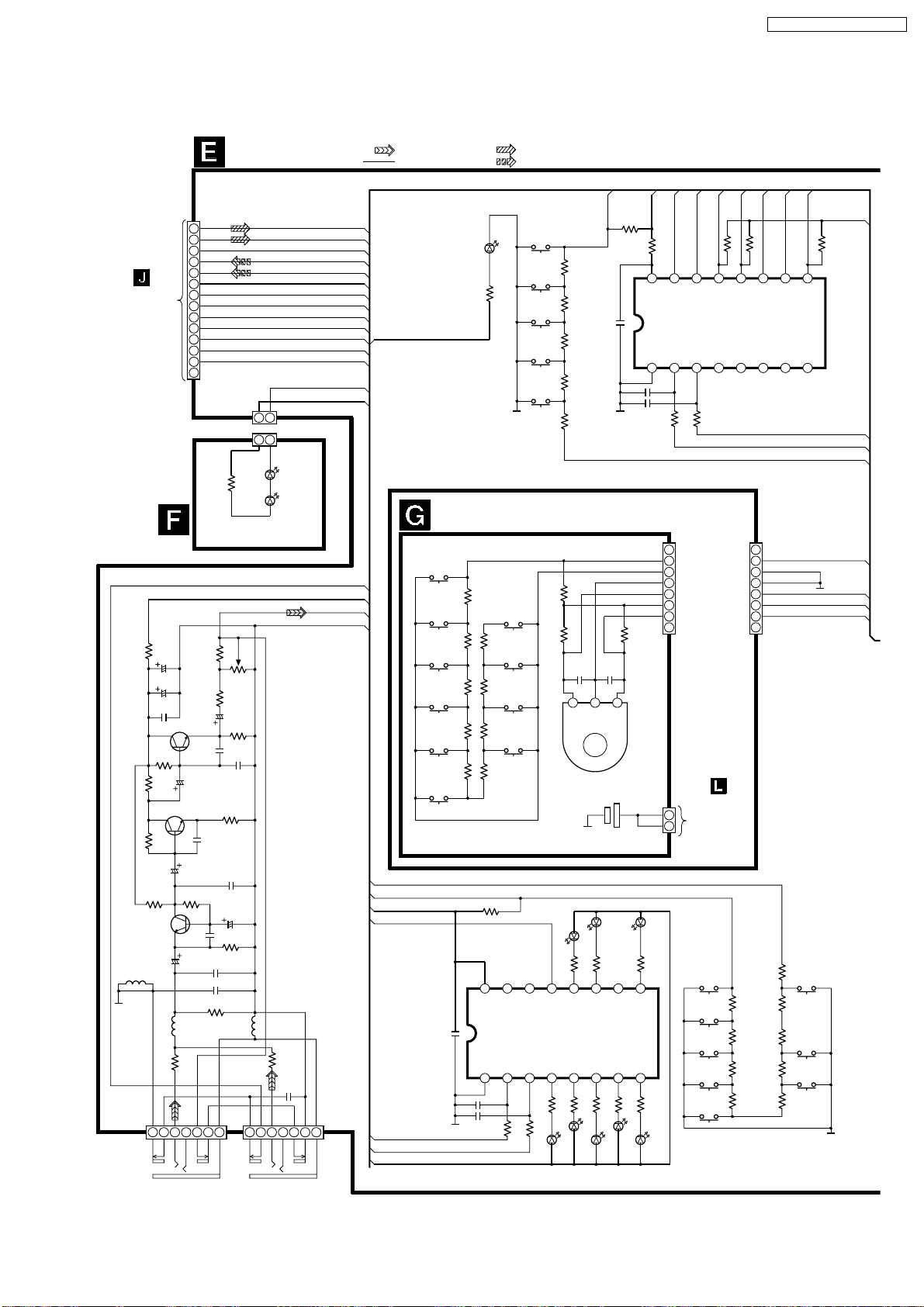
20.4. (E) Panel Circuit, (F) LED Circuit & (G) Tact Switch Circuit
SCHEMATIC DIAGRAM - 26
PANEL CIRCUIT
: +B SIGNAL LINE : RECORD SIGNAL LINE
: PLAYBACK SIGNAL LINE: MIC SIGNAL LINE
SA-VK61DGC / SA-VK61DGCS
TO
DECK CIRCUIT
(CN1001) ON
SCHEMATIC
DIAGRAM - 33
LED
CIRCUIT
R694
C667
330
10V100
C685
16V220
C666
1000P
R682
330K
R684
8.2K
Q607
R690
330K
C670
50V0.33
R937
2.2K
Q900
C918
50V3.3
L610
G0C470JA0030
L608
R970
680
4
5
PBL
14
PBR
13
AGND
12
REC_L
11
REC_R
10
+15V
9
REC_01
8
MOT10V
7
PL_GND
6
DMT
5
DECK1_H
4
BP1
3
MOT_01
2
1
CP603
1
1
R649
560
D630, 631
B3ACA0000234
R696
8.2K
VR602
R695
100
C668
50V1
C665
100P
C663
50V1
C662
0.047
C919
470P
C669
C681 0.022
R972
G0C3R3JA0030
7
6
3
0.01
560
R683
47
C917
1000P
C916
50V4.7
R939
4.7K
L607
1
R697
4.7K
C664
1000P
4
5
Q606
R938
470K
G0C100JA0030
2
MIC1 MIC2
W601A
2
2
W601B
D631
D630
VR602
EVUF2AF25B14
Q606
KTC3199GRTA
MIC AMP
Q607
2SC1740SSTA
MIC AMP
Q900
2SC1740SSTA
LIMITTER
R969
680
C682
0.022
7
2
1
6
3
REC_01
MOT10V
PL_GND
DECK1_H
MOT_01
LED_DVD
DVREF+
MIC_GND
JK900JK600
PBL
PBR
AGND
REC_L
REC_R
+15V
DMT
BP1
MICSW
+9V
MIC
SYS6V
HP_SW
K3
VREF+
LED_DVD
SERC
SERD
LED9V
S601
SLI325URCT31
R600
4.7K
POWER
S602
DOLBY PRO
LOGIC
S603
SUPER
SURROUND
S604
DECK 1/2
S605
REC
D600
TACT SWITCH CIRCUIT
S901
REW
S910
DISPLAY
S909
DECK1
S908
AUX
S907
TAPE
14
1516
MBP2
MBP1
C1BB00000574
DAT
CLK
2
3
100
R732
R900
10K
R912
47K
13512
DVD
LED_
IC604
I/O EXPANDER
LED_
DISC1
4
3.3K
R700
D621
R901
S902
CD PLAY
R902
S903
TUNER/BAND
R903
1.2K
S904
FF
R904
1.8K
S905
STOP
R905
2.2K
S906
DECK2
C636
0.1
1K
1K
R670 10K
C634 100P
C635 100P
R909
10K
R908
6.8K
R907
4.7K
R906
2.7K
VCC
GND
1
R731
100
R601
1K
R602
1K
R603
1.2K
R604
1.8K
R605
2.2K
C901
100P
3
COMB
VR600
EVEKE2F3524M
VOLUME JOG
RMBX0031
D629
1.8K
R708
11
LED_
SSEQ
LED_
DISC2
LED_
6
3.3K
3.3K
R701
R702
D622
D623
D621 - 625
B3ACA0000234
C679
C902
100P
LED_
DISC3
K1
0.1
BS4
D628
R707
SS
R703
R681
10K
C673 100P
C678 100P
VJOG_B_1
VJOG_A_1
12
A
2.7K
10
SW
LED_
LED_
DISC4
7
3.3K
D624
VREF+
VCC
GND
1
R6131KR614
K2
VREF+_1
R913
47K
H901/
W901
D626
R705
9
DPL
LED_
LED_
DISC5
8
3.3K
R704
D625
PL1
PL2
R612
100
14
1516
2PL
1PL
C1BB00000574
DAT
CLK
2
3
1K
8
7
6
5
4
3
2
1
CP900 CN900
TO
POWER
SUPPLY
2
CIRCUIT
1
(CN900) ON
SCHEMATIC
DIAGRAM - 35
D626 - 629
B3ACA0000234
2.7K
S606
CD OPEN/
CLOSE
S607
DISC1
S608
DISC2
S609
DISC3
S610
DISC4
REC_H
DECK1_H
R623 4.7K
13512
H1
REC
IC601
I/O EXPANDER
EC_CTL1
EC_CTL2
4
R661
1K
R662
1K
R663
1.2K
R664
1.8K
BP1
R622 4.7K
10
11
BP1
EC_CTL3
6
8
K2
7
GND2
6
5
VOL_B
4
VREF+
3
VOL_A
2
1
R669
10K
R668
6.8K
R667
4.7K
R666
2.7K
R665
2.2K
MOTOR
1N
ECMUTE
7
DISC5
S614
SEQ
S612
SSEQ
S611
DMT
9
DMT
DECK1
8
R617
4.7K
SW5V
SERA
SERC
MICSW
VOL_B
VREF+
VOL_A
K2
93
Page 94

SA-VK61DGC / SA-VK61DGCS
SCHEMATIC DIAGRAM - 27
PANEL CIRCUIT
C641
50V22
D615
B0ACCE000003
PCNT
23456
1
D601
B0AACK000004
(GCSS ONLY)
D620
B0AACK000004
D606
B0AACK000004
(GCSS ONLY)
D605
B0AACK000004
(GCSS ONLY)
D604
B0AACK000004
D603
B0AACK000004
D602
B0AACK000004
: -B SIGNAL LINE
: +B SIGNAL LINE
FL600
A2BD00000071
FL DISPLAY
8 9 10 11 12 13 14 15 16 17 18 19 20 21 22 23 24 25 26 27 28 29 30 31 32 33 34 35 36 37 38 39 40 41 42 43 44 45 46 47 48 49 50 51 52 53 54
7
C642
50V22
KEYLAT/REGIN
B0ACCE000003
SYS6V
PLLD_IF
VOL_A
VOL_B
SD
SP_C
SP_B
SP_A
DVD_MUTE
SERB
SERC
SERD
PLLDA
VREF+
MUTE_A
PLLCE
DSP_CS
DSP_RST/
SERE
VOL_CS+
C651 1000P
R626
10K
D614
C645 560P
C646 100P
R627
22K
C603
330P
R687 220
R679 220
R632 10K
R634 10K
R645 10K
R686 1K
C648 100P
C647 560P
C643
10V22
C674 0.1
R678 1K
787980
SD
VOL_B
VOL_A
81
SP_C
82
SP_B
83
84
85
86
87
88
89
90
91
92
93
94
95
96
97
98
99
100
L600
RLQB3R3KT-1Y
C627
0.01
(TU_SIG_DEC_IN)
SP_A
DVD_MUTE
SERB
(EX3CK/PLLCK)
SERC (EXDECK_DA/EX1_DA/EX3_DA)
SERD (EX1CK/EX2_DA/EE_DA)
PLLDA
VSS
VDD2
MUTE_A
PLLCE
DSP_CS
DSP_RST/
SERE (DSP_DA/
6CHVOL_DA/KEYCON_DA)
VOL_CS+
SERF (DSPCK/6CHVOLCK/KEYCONCK)
DVD_CMD
DVD_STA
DVDCLK
EECS
SERA (EXDECKCK/
EX2CK/EECK)
CHG_HALF
2
3
1
75
74
77
73
72
76
VDD3
SEG31
SEG32
SEG33
SEG30
(PLL_DA_IN/ST) PLLD_IF
CHG_CW
CHG_CCW
CHG_PLGR
DCDET
NJU_LAT
67
PCNT
9
8
4
5
68
70
69
71
SEG27
SEG28
SEG29
C2BBHF000076 (GC)
C2BBHF000077 (GCS)
MICROPROCESSOR
KARA_LA/REGIN
RESET
XCin
12
10
11
C607 0.1
13
67
SEG26
IC600
XCout
VSS
14
66
SEG25
CF1 (Xin)
15
65
SEG23
SEG24
CF2 (Xout)
16
C606
64
17
0.1
63
SEG22
VDD1
18
61
62
SEG21
SEG19/REG10
SEG20/REG11
KEY3
KEY2
KEY1
19
20
C654 560P
C672 560P
59
60
58
SEG18/REG9
SEG17/REG8
CHG_AD1
CHG_AD2
21
23
22
C653 560P
SEG16/REG7
SPE
57
54
56
55
53
52
SEG11/REG2
SEG15/REG6
SEG14/REG5
SEG13/REG4
SEG12/REG3
DECK2 (RINHF/MODE2/
RINHR/HALF2)
DECK1 (MODE1/HALF1)
DECK3 (PHOTO1/PHOTO2)
CHG_SW (CHG_SW1/CHG_SW2)
SYNC
27
24
26
25
28
29
C680 560P
C675 4700P
C676 4700P
C677 4700P
51
VP
SEG9
SEG10/REG1
SEG8
SEG7
SEG6
VDD3
SEG5
SEG4
SEG3
SEG2
SEG1
GRD11
GRD10
GRD9
GRD8
GRD7
GRD6
GRD5
GRD4
GRD3
GRD2
RMT
GRD1
30
C605
6.3V100
50
49
48
47
46
45
44
43
42
41
40
39
38
37
36
35
34
33
32
31
C600
10V1000
R630
680
D610
MA2C72300F
SYS6V
D611
SERF
R652 100
R660 100
R671 100
DVD_CMD
DVD_STA
DVDCLK
R631
47K
D611
B0ACCE000003
EECS
SERA
CHG_HALF
CHG_CW
CHG_CCW
R637 1K
R647 100
CHG_PLGR
DCDET
NJU_LAT
PCNT
KEYLAT_REGIN
XCIN
XCOUT
94
R628 100
R629 100
R633 100
XIN
XOUTK3K2K1CHG_AD1
R635 1K
CHG_AD2
SPE
DECK2
DECK1
DECK3
CHG_SW
RMT
Page 95

SCHEMATIC DIAGRAM - 28
PANEL CIRCUIT
R712 100K
R713 100K
R714 100K
R715 100K
R716 100K
R717 100K
R718 100K
R719 100K
R720 100K
R721 100K
R722 100K
R723 100K
R724 100K
R725 100K
R726 100K
R727 100K
R728 100K
R729 100K
R730 100K
: -B SIGNAL LINE
: +B SIGNAL LINE
SA-VK61DGC / SA-VK61DGCS
: MAIN SIGNAL LINE
HPL
HPR
HP_SW
C620
L603
L602
L609
0.022
C621
0.022
4
2
3
5
HEADPHONE
C619
0.047
6
7
L604
1
JK601
L602, 603
RLQZP101KT-Y
L604
RLQZP100KT-Y
L609
RLQZP100KT-Y
C622 0.022
C623 330P
R673 22K
R674 22K
C624
330P
EECS
SERA
VREF+
364
IC602
BR93LC46FE2
EEPROM IC
(NOT SUPPLIED)
78
5
R675
2.2K
95
18
17
GND
BIASC
1
C661 50V0.1
SPE
C656
0.01
16
15
NC
TEST
AOUT
VREFC
2
IC603
C1BB00000086
SPECTRUM ANALYZER
RREFCNCDIFOUTNCCIN
4
3
R680
100K
C660 50V0.1
14
SEL
5
SERD
12
13
NC
6
SP_C
12
C
7
C659 50V0.1
SP_B
SP_A
10
11
B
AIN
8
9
C658 50V0.1
DVREF+
A
VCC
C657
0.01
SPEA
R685
100
Page 96
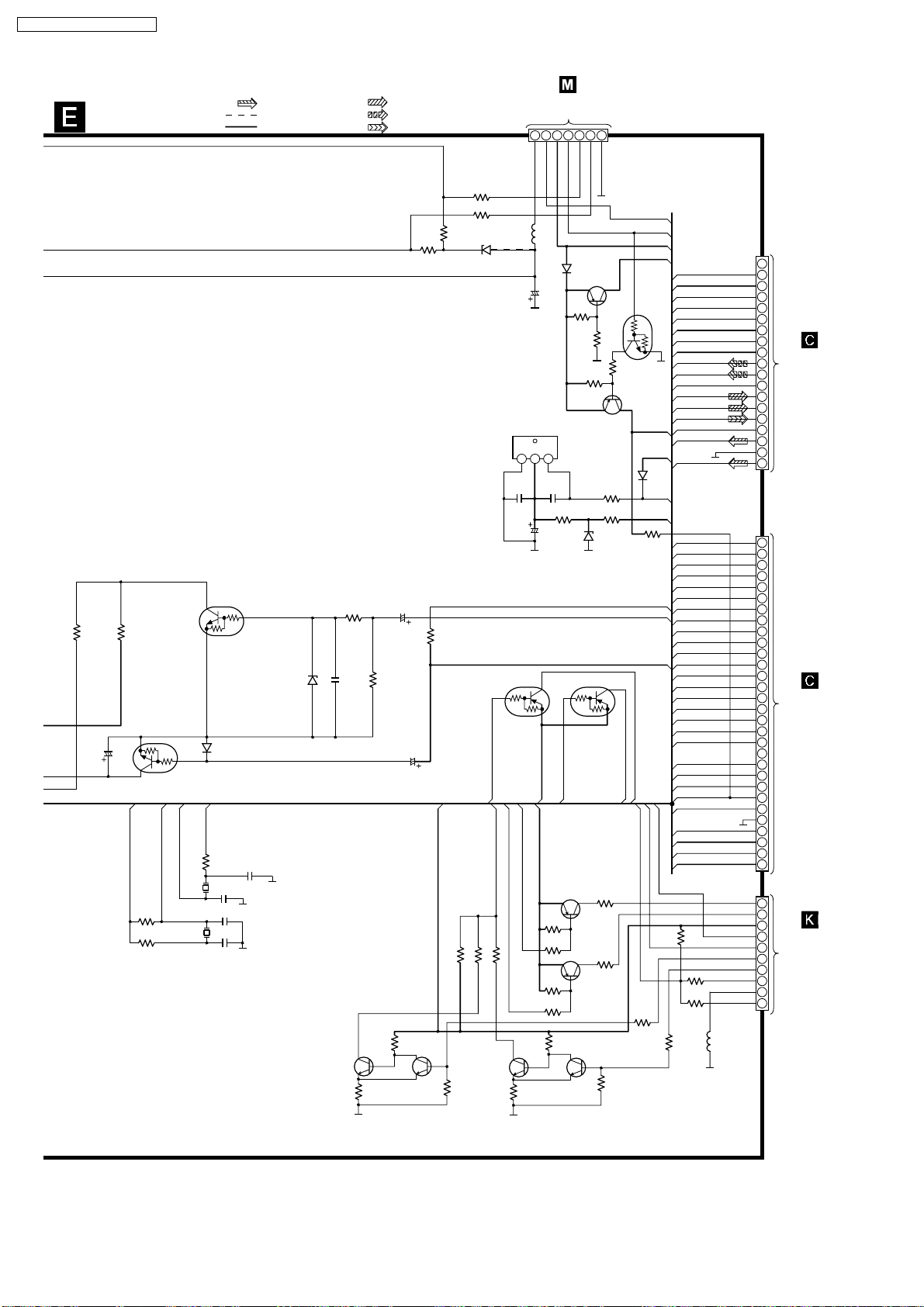
SA-VK61DGC / SA-VK61DGCS
SCHEMATIC DIAGRAM - 29
PANEL CIRCUIT
KRC102MTA
SYNC SWITCH
R639
22K
XCOUT
Q600
R643
10M
R644
330
Q616
XCIN
XIN
X601
X602
H2A100500006
H0A327200073
D617
B0AACK000004
Q600
B1GACFLL0007
RESET SWITCH
XOUT
R640
680
C611
39P
C617
22P
C618
22P
X601
X602
R636
10K
C608
50V0.1
: MAIN SIGNAL LINE
: -B SIGNAL LINE
: +B SIGNAL LINE
Q616
D632
B0AACK000004
C612
39P
R638
4.7K
C609
0.01
Q613
R918
47
KTC3199GRTA
: PLAYBACK SIGNAL LINE
: RECORD SIGNAL LINE
: MIC SIGNAL LINE
R656
R657
47
47
B0BA5R600016
Q603
B1ACCF000063
SUPPLY SWITCH
Q605
KRC102MTA
PCONT SWITCH
Q604
B1ACCF000063
SUPPLY SWITCH
C625
35V4.7
R658
100K
B1GCCFJJ0015
R659
10K
C610
50V4.7
DVREF+
R711 10K
R916
100K
Q612
R917
56K
Q612, 613
SWITCH
TO
POWER CIRCUIT
(CN954) ON
SCHEMATIC DIAGRAM - 37
1
-VP
R676
1
R677
1
L601
G0C100JA0030
D613
C640
50V3.3
D612
B0ACCE000003
Z600
B3RAB0000025
REMOTE SENSOR
G
VDD
231
C637
0.01
Q608
SWITCH (MOTOR)
Q608 Q609
MOTOR
PL1
PL2
DECK3
R709 22K
R710 12K
Q611
R915
47
KTC3199GRTA
4
3
5
2
FL1
PCNT
SYNC
SYS6V
D612
Q603
R650
470K
R654
470K
O
C638
1000P
R699
22
C639
6.3V47
D633
B0BA5R000004
Q609
B1GCCFJJ0015
SWITCH (REC:H)
SW5V
REC_H
MOT10V
Q614, 615
KTA12710YTA
PLUNGER ON/OFF
SWITCH
Q614
R689
22K
R691
1K
Q615
R693
22K
R698
1K
R911
100K
Q610
Q610, 611
SWITCH
6
FL2
7
GND2
R651
Q604
D633
R688
2.7
R692
2.7
H600/W600
10K
R653
4.7K
R672
100
R655
22
MA2C700A0F
R914
56K
Q605
D616
REC_01
MOT_01
R925
SYNC
PCNT
SYS6V
VREF+
DVREF+
VREF+
D616
SYS6V
R648
5.6K
DCDET
SYNC
VREF+
DECK1
DECK2
100
RMT
PL_GND
R921
10K
SPEA
+9V
NJU_LAT
PL_GND
VREF+
LED9V
MUTE_A
+15V
REC_R
REC_L
AGND
PBR
PBL
MIC
MIC_GND
HPR
HPL
SERE
DSP_RST/
VOL_CS+
DSP_CS
SERF
PLLCE
DVD_CMD
PLLDA
DVD_STA
SERC
DVDCLK
SERB
CHG_HALF
DVD_MUTE
CHG_CW
SERA
CHG_CCW
PLLD_IF
CHG_PLGR
DCDET
SERD
KEYLAT/REGIN
SD
CHG_AD1
CHG_AD2
SW5V
CHG_SW
MOT10V
R923
22K
R924
12K
R922
100
HPGND
PPL1
PPL2
DVREF+
PL_GND
DECK2
PPHOTO_1
PPHOTO_2
HALF_PB
MODE_PB
L605
RLQZP100KT-Y
19
18
17
16
15
14
13
12
TO
11
MAIN CIRCUIT
10
(CN601) ON
SCHEMATIC
9
DIAGRAM - 14
8
7
6
5
4
3
2
1
CP601
1
2
3
4
5
6
7
8
9
10
11
12
13
TO
14
MAIN CIRCUIT
15
(CN602) ON
16
SCHEMATIC
17
DIAGRAM - 16
18
19
20
21
22
23
24
25
26
27
28
29
30
CP602
1
2
TO
3
DECK
4
MECHANISM
5
CIRCUIT
6
(CN971) ON
7
SCHEMATIC
DIAGRAM - 33
8
9
10
CP600
96
Page 97
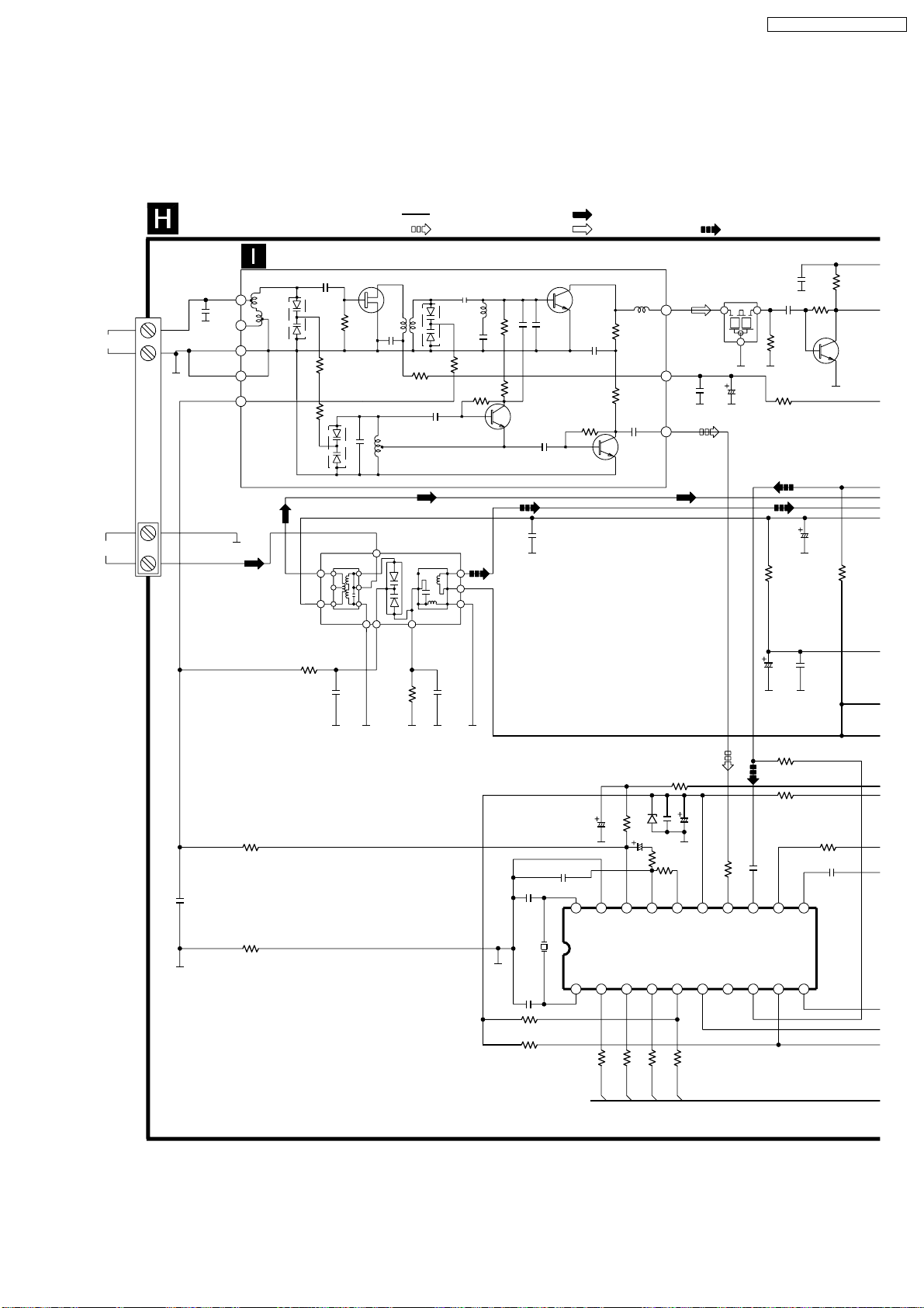
20.5. (H) Tuner Circuit
SCHEMATIC DIAGRAM - 30
SA-VK61DGC / SA-VK61DGCS
FM EXT ANT
UNBALANCED
75 OHM
JK101
AM LOOP
ANT
AM EXT
ANT
TUNER CIRCUIT
1
C150
0.01
1
2
3
4
2
3
4
5
TUNER PACK CIRCUIT
2.7K
R110
1K
5.6P
100K
RLA2Z007-T
AM ANT COIL
3
2
2
1
1
C107
0.047
2SK544
RF AMP
100K
Z101
2.2P
0.001
220
3
4
5
6
9
3
2
1
AM OSC COIL
8
7
C108
R112
8P
100K
: +B SIGNAL LINE
: FM OSC SIGNAL LINE
2.2P
1.2u
820K
560K
3.3P
390
180P
100K
4.7P
4
5
6
2SC2786M
FM MIXER
10P
2SC1675L1L2
BUFFER AMP
LOCAL OSC
2.2P
C136
1000P
: AM SIGNAL LINE
: FM SIGNAL LINE
0.47u
390
0.001
390
10P
680K
: AM OSC SIGNAL LINE
C103
2
C102
16V100
0.01
3
C104
1000P
R105
470
R103
270
R118
3.3K
C127
16V22
2SC2058SPTA
CF201
7
6
8
RLFFETWND01M
1
C101
0.01
R106
470K
Q101
SWITCHING
C114
50V3.3
R119
3.3K
C126
1
R107
330
Q101
C110
0.01
R114
5.6K
R152
R117
D101
B0BC5R000009
R113
C125
10K
16V22
C112
0.01
C133
27P
20 19
0
X103
C134
27P
R138 3.3K
R130 10K
RSXC7M20S05T
Xout
Xin
R137
1K
18
VSS
CE
3
21
R136
1K
CE
PLLDA
C111
50V4.7
R115
560
AOUT
DI
R135
1K
D101
R116
17
AIN
CL
4
R134
PLLCLK
470
1K
C132
R111
390
1000P
16
PD
IC102
DO
DO/ST
C130
6.3V100
15
65
VDD
AM
R151
82
14
FMIN
LW
47K
R128
82
C113
1000P
13
8
LC72131MDTRM
PLL IC (TUNER)
AMIN
SDC
12
IC102
MONO
STRQ
97
11
IFIN
FM
10
R129
27K
C124
100P
97
Page 98
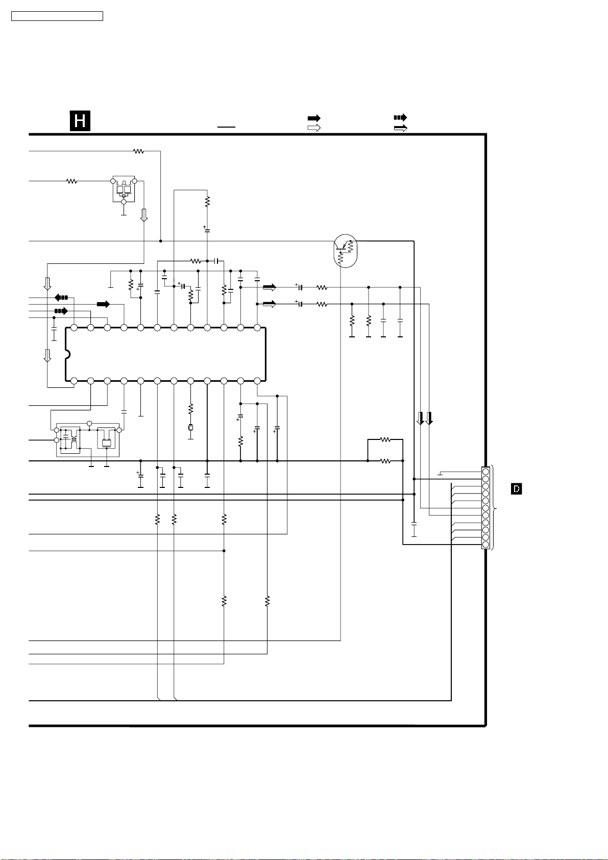
SA-VK61DGC / SA-VK61DGCS
SCHEMATIC DIAGRAM - 31
C109
2
1
R101
0
24
1000P
1
G2BAE0000003
TUNER CIRCUIT
CF202
RLFFETWND01M
1
2
R120
47K
22
23
OSC OUT
FM IF in
Z102
3
6
2
OSC
AM MIX out
3
AFC
REG
5
C106
0.01
21
4
4
C129
6.3V100
AM RF in
AM IF in
R104
1K
3
: +B SIGNAL LINE
R121
22K
C120
16V10
C138
R143
0.01
22K
C139
50V4.7
680P
C119
C115
C116
50V4.7
R102
0.033
4.7K
20
19
18
AGC
AM OUT
DET OUT
IC101
GND
5
ST
SD
6
7
0.01
C148
R125
R126
470
1K
17
C147
1000P
PILOT IN
FM DET
8
R124
C131 150P
16
MPX IN
VCC
9
33
X102
RLFDFT22DD
R123
68K
C149
0.1
15
PILOT OUT
STRQ
10
R127
470
C118
0.01
C137 3300P
14
13
Rch
FM/AM
12
11
C122
50V1
R122
2.7K
C117
0.01
Lch
LA1833NMNTLM
IF & MPX IC
(TUNER)
Mono
C123 50V1
C121 50V0.47
C142
50V1
C141
50V1
IC101
: FM SIGNAL LINE
Q106
B1GCCFJJ0015
TUNER SUPPLY
SWITCH
R142
6.8K
R141
6.8K
100K
R145
R146
: AM SIGNAL LINE
: AM OSC SIGNAL LINE
: FM/AM SIGNAL LINE
C143
C144
100K
4700P
4700P
R144
120
R131
120
C128
TGND
11
15V
10
SD
9
DO/ST
DET_OUT
RCH
LCH
0
PLLDA
PLLCLK
CE
7.5V
TO
8
TUNER EXTENT
7
CIRCUIT
6
(CP702) ON
5
SCHEMATIC
4
DIAGRAM - 14
3
2
1
CP100
R132
10K
SD
DO/ST
R133
1K
98
Page 99
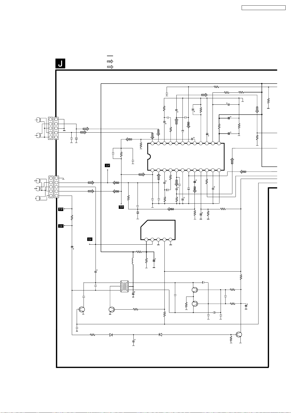
20.6. (J) Deck Circuit & (K) Deck Mechanism Circuit
SCHEMATIC DIAGRAM - 32
: +B SIGNAL LINE
: RECORD SIGNAL LINE
DECK CIRCUIT
: PLAYBACK SIGNAL LINE
SA-VK61DGC / SA-VK61DGCS
PLAYBACK
HEAD
RECORD/PLAY
HEAD
ERASE
HEAD
R1038
R1055
4.7M
R1029
16V10
C1056
ALC T
REC/PB SW
100
16V10
R1030
C1042
HI/LO
AB SW
16V22
10V22
C1045
R1031
2.2K
220
R1090
13
CRO/NOR
RIPPLE
FILTER
OUTPUT
27K
VCC
GND
R1035
10K
C1038
220P
R1015
C1034
47
50V3.3
IC1001
1
1
L
2
3
4
5
R
CS1001
1
2
L
3
4
R
5
CS1002
R
2
3
L
4
5
C1012
1000P
1
2
3
4
5
11
12
50V2.2
C1002
R1001
1
C1015
1000P
C1020
470P
4
5
AN7348S-E1
P.B EQ/REC AMP/
ALC/TPS AMP
R1009
18K
R1010
3
18K
R1017
8.2K
C1019
1000P
R1026
1K
C1021
470P
C1022
1000P
C1023
VCC
12345
C1032
0.018
C1030
10V100
3.9K
R1018
21222324
NF
INPUT
INPUT
TAPE A
TAPE A
PB AMP
PB AMP
IC1001
TAPE B
INPUT
PB AMP
INPUT
C1027
1000P
C1031
10V100
R1016
C1033
0.018
47
NF
TAPE B
1234
1000P
IC1004
SW
GND
CTRL2
0.033
C1036
EQ
PB AMP
OUTPUT
PB AMP
EQ
PB AMP
OUTPUT
5206197188179161015111412
3.9K
R1019
C1035
C1058 1000P
50V3.3
10K
R1022
C1AA00000612
CTRL1
1000P
C1057
CUT
REC IN
ALC LOW
AB SW T
REC IN
220P
C1039
C1037
50V3.3
IC1004
R/P SELECT
C1043
C1040
16V10
R1028
50V4.7
REC OUT
REC OUT
C1041
8.2K
4.7K
C1044
10V33
C1059
0.01
C1046
10V220
R1039
15K
R1040
R1098
10K
0
R1032
10K
C1007
4700P
C1003
1500P
Q1001
C1001
0.01
R1003
Q1001
B1ABCF000131
SWITCHING
(BEAT PROOF)
10K
C1006
50V1
Q1003
L1001
G0C470JA0030
L1002
7L1A62N
6
5
4
D1003
B0ACCK000005
Q1003
B1AAGC000007
SWITCHING
(RECH)
C1008
50V1
R1005
4.7K
3
2
1
C1010
25V100
R1004
1.5K
C1009
10V47
R1006
1K
D1004
B0BC3R700004
Q1004-Q1005
B1AAGC000007
BIAS OSCILLATOR
C1011
0.047
R1007
4.7
C1014
1000P
Q1004
Q1005
C1013
1000P
C1016
C1017
2200P
2200P
Q1007
B1ABCF000131
BIAS OSC CONTROL
R1011
10K
R1012
4.7K
C1018
0.01
R1013
4.7K
Q1007
R1014
4.7K
C1026
6.3V47
99
Page 100
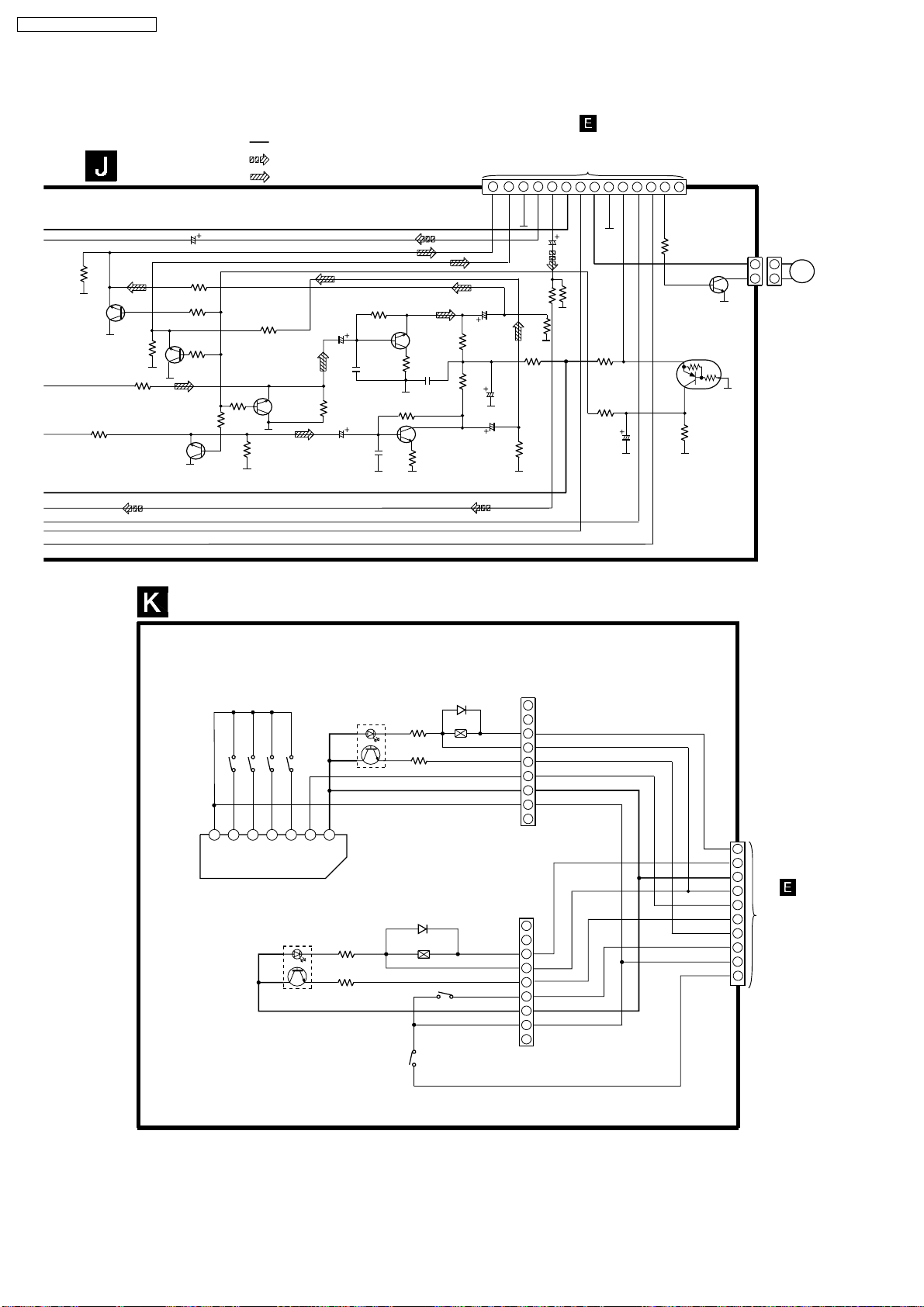
SA-VK61DGC / SA-VK61DGCS
SCHEMATIC DIAGRAM - 33
DECK CIRCUIT
C1054 50V3.3
R1095
100K
Q1020
Q1020-Q1021
B1ABEB000001
MUTING SWITCH
R1086
2.2K
B1ABEB000001
R1096
100K
R1084
2.2K
Q1012-Q1013
MUTING
Q1013
R1091
2.2K
R1094
1K
R1093
1K
Q1021
R1048
1K
: +B SIGNAL LINE
: RECORD SIGNAL LINE
: PLAYBACK SIGNAL LINE
R1092
2.2K
R1047
1K
Q1012
R1046
100K
C1048
50V1
R1045
100K
C1047
50V1
Q1014-Q1015
B1ABCF000011
BUFFER AMP
R1049
1M
Q1014
C1049
1000P
C1050
1000P
R1050
1M
R1051
220
C1060
0.01
Q1015
R1052
220
R1053
680
R1054
680
C1051
50V1
C1052
50V1
14
PBOUTL
C1053
16V220
R1087
47K
13
PBOUTR
AFGND
C1064
50V3.3
R1057
2.2K
R1085
47K
R1056
220
1112
RECINL
TO
PANEL CIRCUIT
(CP603) ON
SCHEMATIC
DIAGRAM - 26
10
+B
MO+B
REC_H
RECINR
10K
R1097
R1058
R1061
6897
2.7K
0
C1055
50V0.1
5
DMT
MO GND
4
2
3
BP1
MOTOR
DECK1_H
R1060
390
Q1017
B1AARC000002
MOTOR SWITCH
B1GDCFJJ0023
DECK MUTING SWITCH
CN1001
1
Q1017
Q1016
R1059
10K
Q1016
1
2
W1002
1
M
2
DECK MECHANISM CIRCUIT
IC971
CNB13030R2AU
PHOTO INTERRUPTER
MODE
RECINH_F
RECINH_R
S975
S974
S971
_F
_R
MODE
RECINH
RECINH
AD_OUT
IC951
CNB13030R2AU
PHOTO INTERRUPTER
1234567
STBY
_5V
R952
820
R953
39K
RGSD12A1445T
VREF
_GND
HALF
S972
HALF
Z971
R972
820
R973
39K
D951
MA2C16500E
PL971
S952
MODE
D971
MA2C16500E
PL970
HALF
MODE
D1_CRO2
GND
PHOTO_T
HALF
STBY_5V
VREF_GND
PHOTO_S
MODE
D1_CRO2
GND
PHOTO_T
HALF
STBY_5V
VREF_GND
PL
PL2
1
PL1
2
STBY_5V
3
PL_GND
4
5
6
7
8
9
10
CN971
TO
PANEL
CIRCUIT
(CP600) ON
SCHEMATIC
DIAGRAM - 29
AD_OUT
PHOTO_PB
PHOTO_RP
HALF_PB
PL
VREF_GND
MODE_PB
S951
100
 Loading...