

Page 1
A
A
CD Stereo System
SA-PMX2E
SA-PMX2EG
Colour
(S)... Silver Type
ORDER NO. MD0703029CE
Specification
n Amplifier Section
RMS OUTPUT POWER both channel driven simultaneously
10% Total harmonic distortion 80 W per channel (4 Ω)
Input Impedance
MUSIC PORT 250 mV 13 kΩ
Output Impedance
HEADPHONE 16 to 32 Ω
Phone jack
Terminal Stereo, 3.5 mm
Music port input jack
Terminal Stereo, 3.5 mm
n FM Tuner Section
Frequency range 87.50 MHz to 108.00 MHz
(50 kHz step)
Sensitivity 10 dBµV (IHF)
S/N 30 dB 10 dBµV
ntenna terminal(s) 75 Ω (unbalanced)
Preset station FM 20 stations
AM 15 stations
n AM Tuner Section
Frequency range 522 to 1629 kHz (9kHz step)
520 to 1630 kHz (10kHz step)
Sensitivity
S/N 20 dB (at 999 kHz) 1778 µV/m
n CD Section
Disc played [8 cm or 12 cm]
(1) CD-Audio (CD-DA)
(2) CD-R/RW (CD-DA, MP3 formatted disc)
(3) MP3
Sampling frequency
CD 44.1 kHz
MP3 32 kHz, 44.1 kHz, 48 kHz
Bit rate
MP3 32 kbps to 384 kbps
Decoding 16/20/24 bit linear
Pickup
Beam source Semiconductor laser
Wavelength 785 nm
Laser power CLASS 1
udio output (Disc)
Number of channels 2 Channel
Frequency response 20 Hz to 20 kHz (+1, -2 dB)
Wow and flutter Below measurable limit
Digital filter 8fs
D/A converter MASH (1 bit DAC)
n USB section
Playable USB Storage Media
(1) HDD
(2) USB MP3 player/Digital audio player
(3) USB Thumbdrives
Supported audio file format
MP3
© 2007 Matsushita Electric Industrial Co. Ltd.. All
rights reserved. Unauthorized copying and
distribution is a violation of law.
Page 2
A
SA-PMX2E / SA-PMX2EG
USB memory port
Maximum current 500mA
Bit rate
MP3 32 kbps to 320 kbps
udio output (MP3)
Number of channels 2 channel
Frequency response (MP3) 20 Hz to 20 kHz
n General
Power supply AC 230 V, 50 Hz
Power consumption 80 W
Dimensions (W x H x D) 174 mm x 244 mm x 318 mm
Mass 4.6 kg
Operating temperature range +5 to +35°C
Operating humidity range 5 to 90% RH (no condensation)
Power consumption in standby mode 0.5 W (approx.)
Notes :
1. Specifications are subject to change without notices. Mass and
dimensions are approximate.
2. Total harmonic distortion is measured by the digital spectrum
analyzer.
n System : SC-PMX2E-S
n System : SC-PMX2EG-S
Music center: SA-PMX2E-S
Speaker: SB-PMX2EG-M
Music center: SA-PMX2EG-S
Speaker: SB-PMX2EG-M
CONTENTS
Page Page
1 Safety Precautions
1.1. GENERAL GUIDELINES
1.2. Before Repair and Adjustment
1.3. Protection Circuitry
1.4. Safety Part Information
2 Prevention of Electro Static Discharge (ESD) to
Electrostatically Sensitive (ES) Devices
3 Precaution of Laser Diode
4 Handling Precautions For Traverse Deck
5 Handling the Lead free Solder
5.1. General description about Lead Free Solder (PbF)
6 Accessories
7 Operation Procedures
7.1. Main Unit Key Buttons Operation
7.2. Remote Control Key Buttons Operation
7.3. Disc Information
8 Self diagnosis and special mode setting
8.1. Service Mode Summary Table
8.2. Service Mode Table
8.3. Error Code Table
9 Assembling and Disassembling
9.1. Caution
9.2. Disassembly flow chart
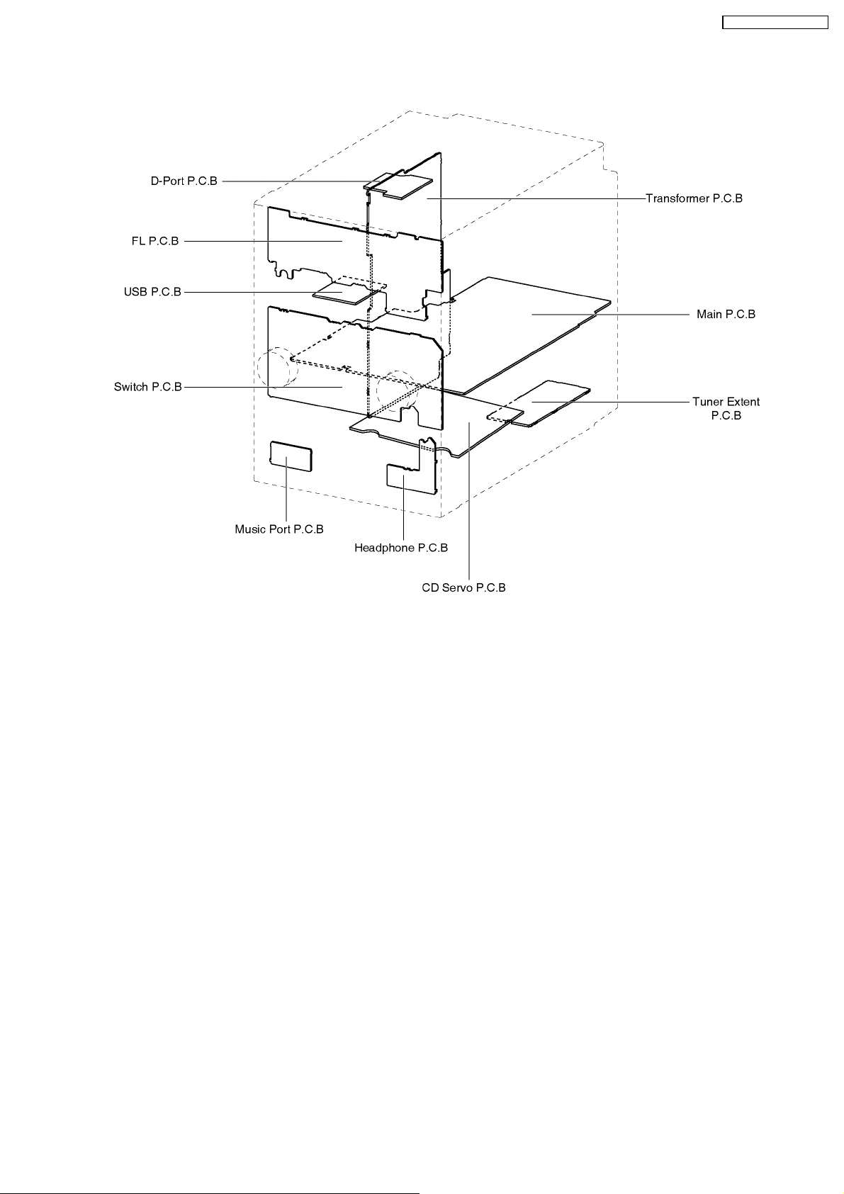
9.3. Main Parts Location Diagram
9.4. Disassembly of Top Panel Unit
9.5. Disassembly of D-Port P.C.B
9.6. Disassembly of USB P.C.B
9.7. Disassembly of Front Panel
9.8. Disassembly of Music Port P.C.B
9.9. Disassembly of FL, Switch & Headphone P.C.B
9.10. Disassembly of Rear Cabinet
9.11. Disassembly of Main P.C.B
4
4
5
5
5
6
7
8
9
9
10
11
11
12
12
13
13
13
21
23
23
24
25
26
26
27
28
29
29
30
30
9.12. Disassembly of Inner Chassis
9.13. Disassembly of CD Mechanism Unit
9.14. Disassembly of Transformer P.C.B.
9.15. Disassembly of Tuner Extent P.C.B.
9.16. Replacement of the Power IC
9.17. Disassembly of Traverse Unit, Driving Gear, and Cam
Gear
10 Service Positions
10.1. Check and Repair of Transformer P.C.B.
10.2. Check and Repair of D-Port P.C.B.
10.3. Check and Repair of FL, Switch, Headphone and Music
Port P.C.B.
10.4. Check and Repair of Main P.C.B.
10.5. Checking and Repairing of CD Servo P.C.B.
10.6. Check and Repair of USB P.C.B (Side B).
11 Voltage Measurement & Waveform Chart
11.1. Voltage Measurement
11.2. Waveform Chart
12 Wiring Connection Diagram
13 Block Diagram
13.1. CD SERVO/ OPTICAL PICKUP UNIT
13.2. MAIN(1/2)/ TUNER EXTENT/ PANEL/ SWITCH/
HEADPHONE/ D-PORT
13.3. MAIN(2/2)/ USB MODULE/ MUSIC PORT/
TRANSFORMER
14 Notes of Schematic Diagram
15 Schematic Diagram
15.1. CD SERVO CIRCUIT
15.2. MAIN CIRCUIT
15.3. TUNER EXTENT CIRCUIT, D-PORT CIRCUIT, MUSIC
PORT CIRCUIT and HEADPHONE CIRCUIT
15.4. PANEL CIRCUIT
31
31
32
32
32
33
37
37
38
39
40
41
42
43
43
47
49
51
51
52
53
55
57
57
58
63
64
2
Page 3

SA-PMX2E / SA-PMX2EG
15.5. SWITCH CIRCUIT 65
15.6. USB CIRCUIT
15.7. TRANSFORMER CIRCUIT
16 Printed Circuit Board Diagrams
16.1. CD SERVO P.C.B and TUNER EXTENT P.C.B
16.2. MAIN P.C.B
16.3. PANEL P.C.B, D-PORT P.C.B, SWITCH P.C.B, MUSIC
PORT P.C.B and HEADPHONE P.C.B
16.4. TRANSFORMER P.C.B and USB P.C.B
17 Illustration of IC 痴, Transistors and Diodes
18 Terminal Function of IC's
18.1. IC800 (C2CBYY000422) IC MICROPROCESSOR
66
67
69
69
70
18.2. IC7001 (MN6627954MA) IC SERVO
PROCESSOR/DIGITAL SIGNAL PROCESSOR/DIGITAL
FILTER D/A CONVERTER
18.3. IC7002 (BA5948FPE2) IC 4CH Drive
19 Exploded Views
19.1. Cabinet Parts Location
71
72
73
19.2. CD Loading Mechanism Parts Location
19.3. Packaging
20 Replacement Parts List
74
74
74
75
77
77
78
79
81
3
Page 4
SA-PMX2E / SA-PMX2EG
1 Safety Precautions
1.1. GENERAL GUIDELINES
1. When servicing, observe the original lead dress. If a short circuit is found, replace all parts which have been overheated or
damaged by the short circuit.
2. After servicing, ensure that all the protective devices such as insulation barriers, insulation papers shields are properly installed.
3. After servicing, check for leakage current checks to prevent from being exposed to shock hazards.
1.1.1. LEAKAGE CURRENT COLD CHECK
1. Unplug the AC cord and connect a jumper between the two prongs on the plug.
2. Using an ohmmeter measure the resistance value, between the jumpered AC plug and each exposed metallic cabine t part on
the equipment such as screwheads, connectors, control shafts, etc. When the expose d metallic part has a return path to the
chassis, the reading should be between 1MΩ and 5.2Ω.
When the exposed metal does not have a return path to the chassis, the reading must be
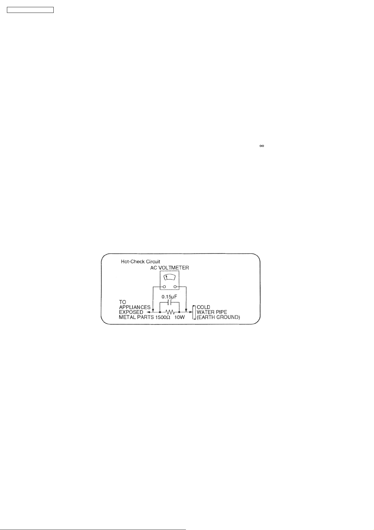
1.1.2. LEAKAGE CURRENT HOT CHECK (See Figure 1.)
1. Plug the AC cord directly into the AC outlet. Do not use an isolation transformer for this check.
2. Connect a 1.5kΩ, 10 watts resistor, in parallel with a 0.15µF capacitors, between each exposed metallic part on the set and a
good earth ground such as a water pipe, as shown in Figure 1.
3. Use an AC voltmeter, with 1000 ohms/volt or more sensitivity, to measure the potential across the resistor.
4. Check each exposed metallic part, and measure the voltage at each point.
5. Reverse the AC plug in the AC outlet and repeat each of the above measurements.
6. The potential at any point should not exceed 0.75 volts RMS. A leakage current tester (Simpson Model 229 or equivalent) may
be used to make the hot checks, leakage current must not exceed 1/2 milliamp. should the measurement is outside of the limits
specified, there is a possibility of a shock hazard, and the equipment should be repaired and re-checked before it is returned
to the customer.
.
Figure. 1
4
Page 5
SA-PMX2E / SA-PMX2EG
1.2. Before Repair and Adjustment
Disconnect AC power, discharge Power Supply Capacitors C500, C501, C513, C625, C626, C633, C634 and C951 through a 10Ω,
1W resistor to ground.
DO NOT SHORT-CIRCUIT DIRECTLY (with a screwdriver blade, for instance), as this may destroy solid state devices.
After repairs are completed, restore power gradually using a variac, to avoid overcurrent.
· Current consumption at AC 230V, 50 Hz in NO SIGNAL mode (volume min) should be ~300 mA.
1.3. Protection Circuitry
The protection circuitry may have operated if either of the following conditions are noticed :
· No sound is heard when the power is turned on.
· Sound stops during a performance.
The function of this circuitry is to prevent circuitry damage if, for example, the positive and negative speaker connection wires are
"shorted", or if speaker systems with an impedance less than the indicated rated impedance of the amplifier are used.
If this occurs, follow the procedure outlines below:
1. Turn off the power.
2. Determine the cause of the problem and correct it.
3. Turn on the power once again after one minute.
Note:
When the protection circuitry functions, the unit will not operate unless the power is first turned off and then on again.
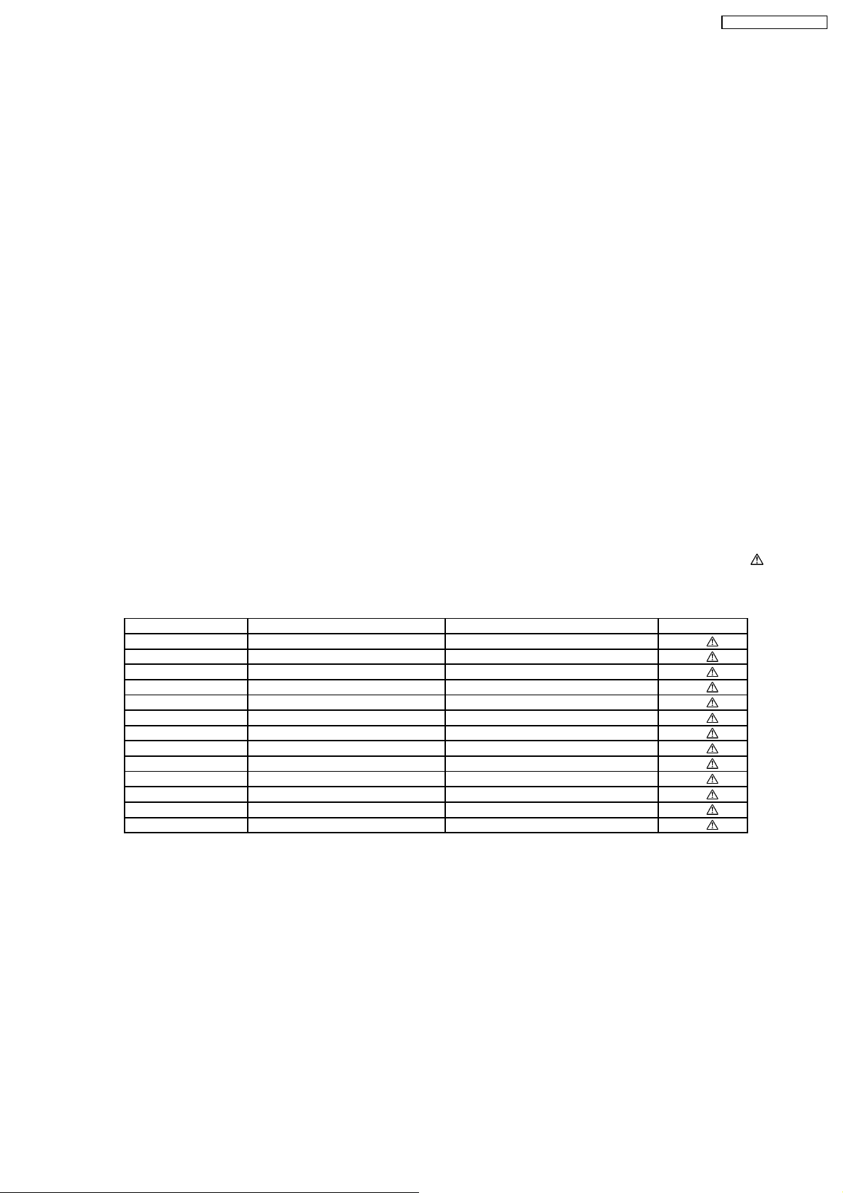
1.4. Safety Part Information
Safety Parts List:
There are special components used in this equipment which are important for safety.These parts are marked by
Schematic Diagrams & Replacement Parts List. It is essential that these critical parts should be replaced with manufacturer’s
specified parts to prevent shock, fire or other hazards. Do not modify the original design without permission of manufacturer.
Table 1
Reference No. Part No. Part Name & Description Remarks
A2 K2CQ2CA00002 AC CORD [M]
F1 K5D102BLA013 FUSE [M]
JK600 K2AA2B000015 AC INLET [M]
T600 G4CYAYY00137 SUB TRANSFORMER [M]
T601 G4CYAYY00150 TRANSFORMER [M]
L600 ELF15N035AN LINE FILTER [M]
RL600 K6B1ADA00011 RELAY [M]
Z600 ERZV10V511CS ZENER [M]
FP600 K5G202A00044 FUSE PROTECT OR [M]
FP601 K5G102A00039 FUSE PROTECT OR [M]
FP602 K5G702Z00004 FUSE PROTECTOR [M]
FP603 K5G702Z00004 FUSE PROTECTOR [M]
FP604 K5G402A00025 FUSE PROTECT OR [M]
in the
5
Page 6

SA-PMX2E / SA-PMX2EG
2 Prevention of Electro Static Discharge (ESD) to
Electrostatically Sensitive (ES) Devices
Some semiconductor (solid state) devices can be damaged easily by electricity. Such components commonly are called
Electrostatically Sensitive (ES) Devices. Examples of typical ES devices are integrated circuits and some field-effect transistors and
semiconductor “chip” components. The following techniques should be used to help reduce the incidence of component damage
caused by electro static discharge (ESD).
1. Immediately before handlin g any semiconductor component or semiconductor-equiped assembly, drain off any ESD on your
body by touching a known earth ground. Alternatively, obtain and wear a commercially available discharging ESD wrist strap,
which should be removed for potential shock reasons prior to applying power to the unit under test.
2. After removing an electrical assembly equiped with ES devices, place the assembly on a conductive surface such as aluminium
foil, to prevent electrostatic charge build up or exposure of the assembly.
3. Use only a grounded-tip soldering iron to solder or unsolder ES devices.
4. Use only an anti-static solder removal device. Some solder removal devices not classified as “anti-static (ESD protected)” can
generate electrical charge to damage ES devices.
5. Do not use freon-propelled chemicals. These can generate electrical charges sufficient to damage ES devices.
6. Do not remove a replacement ES device from its protective package until immediately before you are ready to install it. (Most
replacement ES devices are packaged with leads electrically shorted together by conductive foam, aluminium foil or
comparable conductive material).
7. Immediately before removing the protective material from the leads of a replacement ES device, touch the protective material
to the chassis or circuit assembly into which the device will be installe d.
Caution
Be sure no power is applied to the chassis or circuit, and observe all other safety precautions.
8. Minimize bodily motions when handling unpackaged replacement ES devices. (Otherwise harmless motion such as the
brushing together of your clothes fabric or the lifting of your foot from a carpeted floor can generate static electricity (ESD)
sufficient to damage an ES device).
6
Page 7
SA-PMX2E / SA-PMX2EG
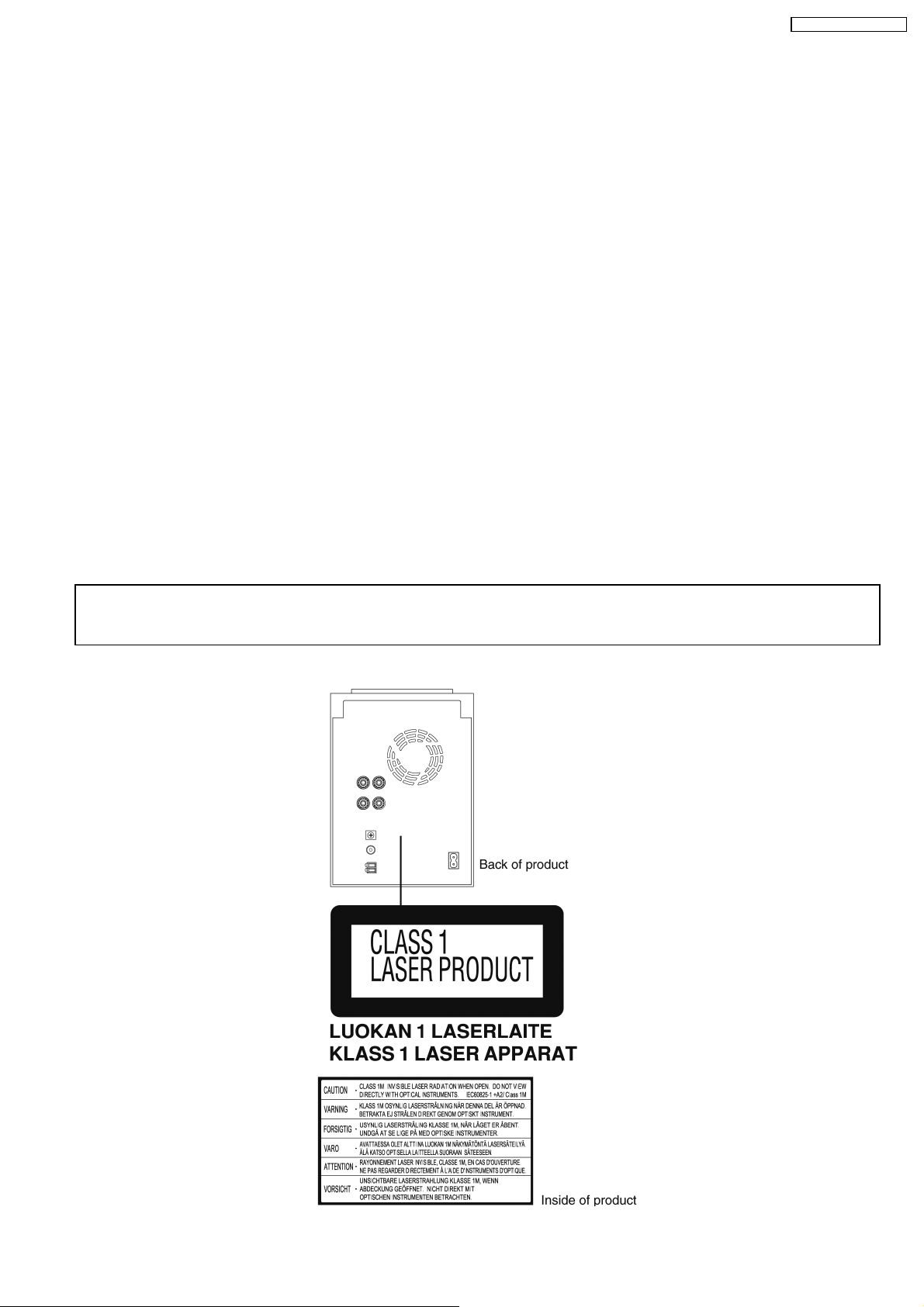
3 Precaution of Laser Diode
Caution :
This product utilizes a laser diode with the unit turned "ON", invisible laser radiation is emitted from the pick up lens.
Wavelength : 780 nm
Maximum output radiation power from pick up : 100 µW/VDE
Laser radiation from pick up unit is safety level, but be sure the followings:
1. Do not disassemble the optical pick up unit, since radiation from exposed laser diode is dangerous.
2. Do not adjust the variable resistor on the pick up unit. It was already adjusted.
3. Do not look at the focus lens using optical instruments.
4. Recommend not to look at pick up lens for a long time.
ACHTUNG :
Dieses Produkt enthält eine Laserdiode. Im eingeschalteten Zustand wird unsichtbare Laserstrahlung von der Lasereinheit
abgestrahlt.
Wellenlänge : 780nm
Maximale Strahlungsleistung der Lasereinheit :100 µW/VDE
Die Strahlung an der Lasereinheit ist ungefährlich, wenn folgend e Punkte beachtet werden:
1. Die Lasereinheit nicht zerlegen, da die Strahlung an der freigelegten Laserdiode gefährlich ist.
2. Den werkseitig justierten Einstellregler der Lasereinhit nicht verstellen.
3. Nicht mit optischen Instrumenten in die Fokussierlinse blicken.
4. Nicht über längere Zeit in die Fokussierlinse blicken.
ADVARSEL :
I dette a apparat anvendes laser.
CAUTION!
THIS PRODUCT UTILIZES A LASER.
USE OF CONTROLS OR ADJUSTMENTS OR PERFORMANCE OF PROCEDURES OTHER THAN THOSE SPECIFIED HEREIN MAY RESULT
IN HAZARDOUS RADIATION EXPOSURE.
n Use of Caution Labels
7
Page 8
SA-PMX2E / SA-PMX2EG
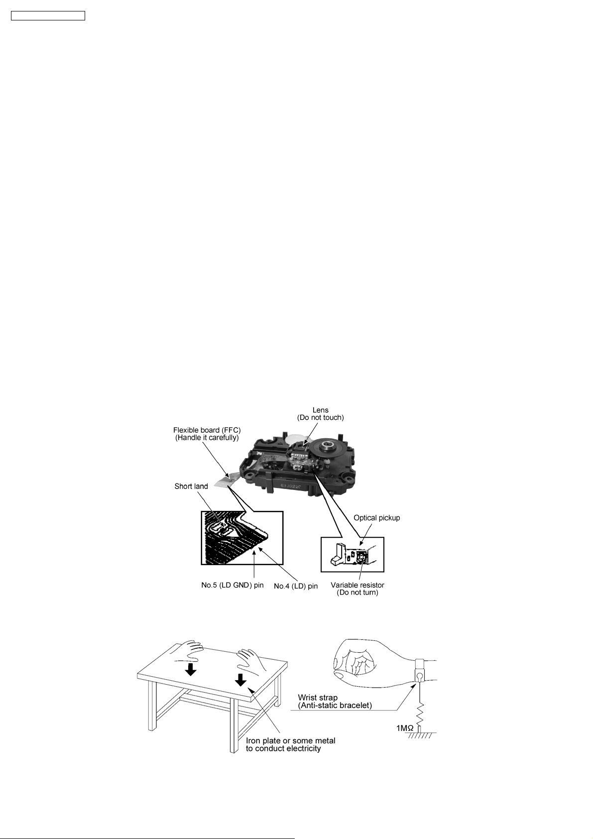
4 Handling Precautions For Traverse Deck
The laser diode in the traverse deck (optical pickup) may break down due to potent ial difference caused by static electricity of
clothes or human body. So, be careful of electrostatic breakdown during repair of the traverse deck (optical pickup).
· Handling of traverse deck (optical pickup)
1. Do not subject the traverse deck (optical pickup) to static electricity as it is extremely sensitive to electrical shock.
2. To prevent the breakdown of the laser diode, an antistatic shorting pin is inserted into the flexible board (FFC board).
3. Take care not to apply excessive stress to the flexible board (FFC board). When removing or connecting the short pin, finish
the job in as short time as possible. (Fig 4.1)
4. Do not turn the variable resistor (laser power adjustment). It has already been adjusted.
· Grounding for electrostatic breakdown prevention
1. Work table grounding. (Fig 4.2)
Use the anti-static wrist strap to discharge the static electricity from your body.
2. Work table grounding. (Fig 4.2)
Put a conductive material (sheet) or steel sheet on the area where the traverse deck (optical pickup) is place, and ground
the sheet.
Caution:
The static electricity of your clothes will not be grounded through the wrist strap. So, take care not to let your clothes touch the
traverse deck (optical pickup).
Caution when replacing the Traverse Deck
The traverse deck has a short point shorted with solder to protect the laser diode against electrostatics breakdown. Be sure to
remove the solder from the short point before making connections.
(Fig 4.1)
(Fig 4.2)
8
Page 9

SA-PMX2E / SA-PMX2EG
5 Handling the Lead free Solder
5.1. General description about Lead Free Solder (PbF)
The lead free solder has been used in the mounting process of all electrical components on the printed circuit boards used for this
equipment in considering the globally environmental conservation.
The normal solder is the alloy of tin (Sn) and lead (Pb). On the other hand, the lead free solder is the alloy mainly consists of tin
(Sn), silver (Ag) and Copper (Cu), and the melting point of the lead free solder is higher approx.30 degrees C (86°F) more than that
of the normal solder.
Definition of PCB Lead Free Solder being used
The letter of “PbF” is printed either foil side or components side on the PCB using the lead free solder.
(See right figure)
Service caution for repair work using Lead Free Solder (PbF)
· The lead free solder has to be used when repairing the equipment for which the lead free solder is used.
(Definition: The letter of “PbF” is printed on the PCB using the lead free solder.)
· To put lead free solder, it should be well molten and mixed with the original lead free solder.
· Remove the remaining lead free solder on the PCB cleanly for soldering of the new IC.
· Since the melting point of the lead free solder is higher than that of the normal lead solder, it takes the longer time to melt
the lead free solder.
· Use the soldering iron (more than 70W) equipped with the temperature control after setting the temperature at 350±30
degrees C (662±86°F).
Recommended Lead Free Solder (Service Parts Route.)
· The following 3 types of lead free solder are available through the service parts route.
RFKZ03D01K-----------(0.3mm 100g Reel)
RFKZ06D01K-----------(0.6mm 100g Reel)
RFKZ10D01K-----------(1.0mm 100g Reel)
Note
* Ingredient: Tin (Sn), 96.5%, Silver (Ag) 3.0%, Copper (Cu) 0.5%, Cobalt (Co) / Germanium (Ge) 0.1 to 0.3%
9
Page 10
SA-PMX2E / SA-PMX2EG
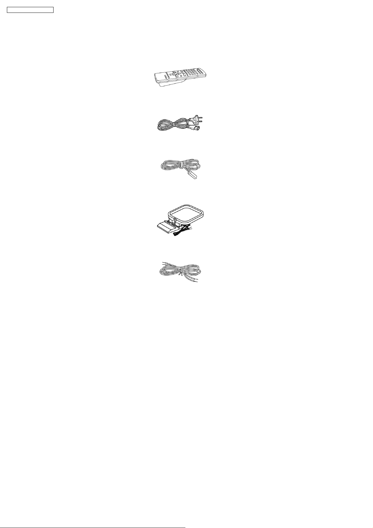
6 Accessories
Note : Refer to Packing Materials & Accessories Parts List (Section 20) for the part number.
Remote Control
AC Cord
FM Antenna
AM Loop Antenna
Wire
10
Page 11
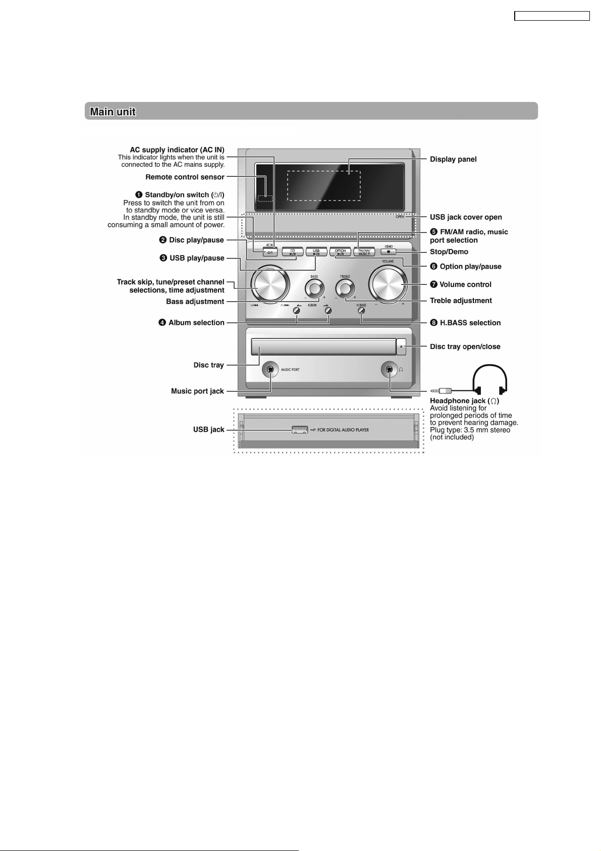
7 Operation Procedures
7.1. Main Unit Key Buttons Operation
SA-PMX2E / SA-PMX2EG
11
Page 12
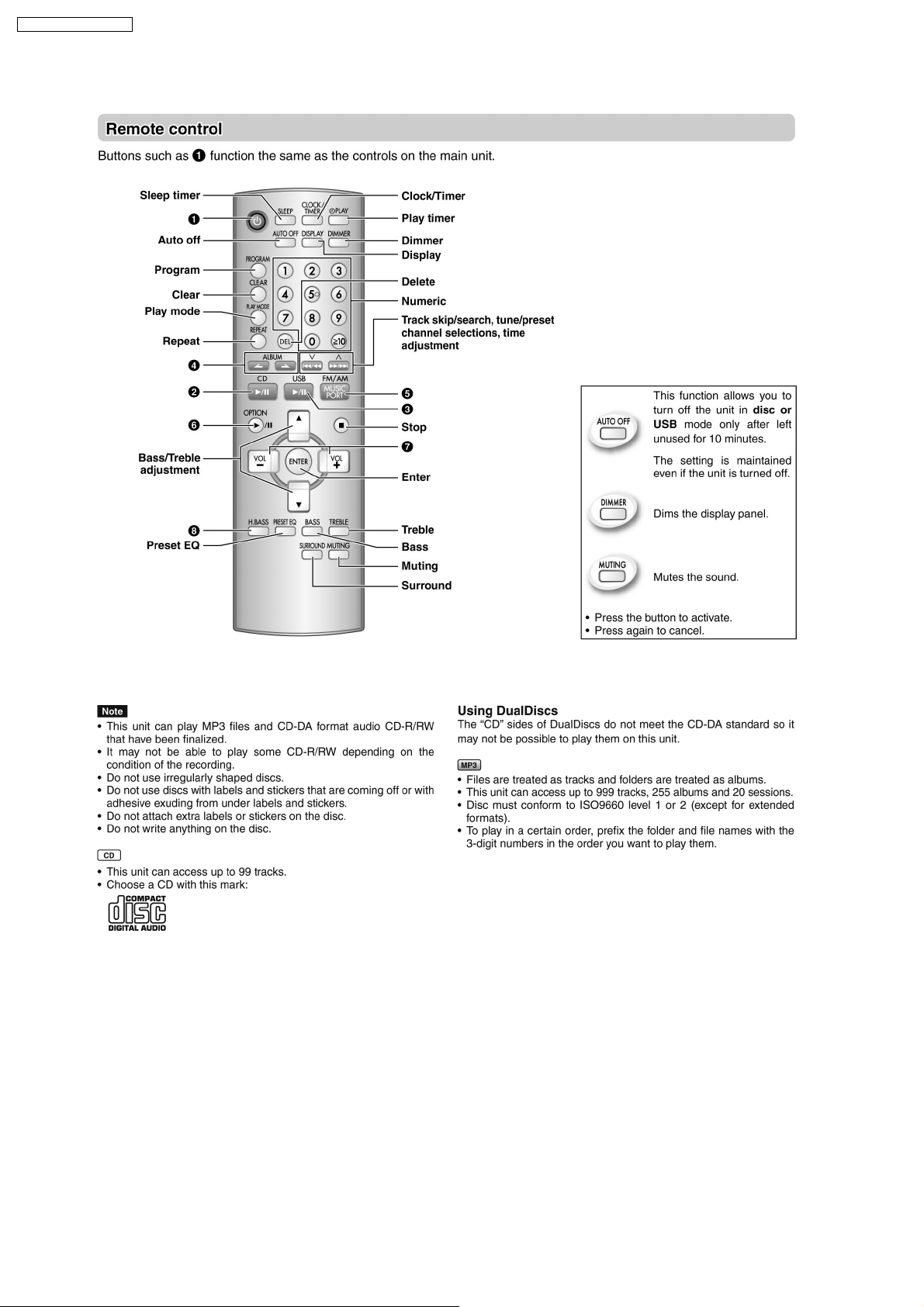
SA-PMX2E / SA-PMX2EG
7.2. Remote Control Key Buttons Operation
7.3. Disc Information
12
Page 13
SA-PMX2E / SA-PMX2EG
8 Self diagnosis and special mode setting
This unit is equipped with features of self-diagnostic & special mode setting for checking the functions & reliability.
Special Note : Checking of the reliability (ageing) & changer operation must be carry out to ensure good working condition
in unit.
8.1. Service Mode Summary Table
The service modes can be activated by pressing various button combination on the main unit and remote control unit.Below is the
summary for the various modes for checking:
Player buttons Remote control unit buttons Application Note
[STOP] [4], [7] Entering into doctor mode (Refer to section .8.2.1. service mode
[STOP]+
[H.BASS]
Mode Remote control unit buttons Application Note
In Doctor Mode [DIMMER] FL ALL Segment inspection (Refer to section .8.2. service mode Table
-- Self-diagnostic mode (Refer to section .8.2.1. service mode
[MUSIC PORT] Tuner Check (Refer to section .8.2. service mode Table
[6] CD Open Test (Refer to section .8.2. service mode Table
[7] Volume 50 setting check (Refer to section .8.2. service mode Table
[8] Volume 29 setting check (Refer to section .8.2. service mode Table
[9] Volume 0 setting check (Refer to section .8.2. service mode Table
[ ], [1], [1] CD Loading Test Mode (Refer to section .8.2. service mode Table
[ ], [1], [2] CD Traverse Unit Test Mode (Refer to section .8.2. service mode Table
[ ], [1], [3] CD Combination Test Mode (Refer to section .8.2. service mode Table
[ ], [1], [4] CD Auto Adjustment Display (Refer to section .8.2. service mode Table
[SLEEP] Cold Start (Refer to section .8.2. service mode Table
[PROGRAM] MP3 Test (Refer to section .8.2. service mode Table
[2] USB Test (Refer to section .8.2. service mode Table
Table 1 for more information.)
Table 1 for more information.)
1 & 2 for more information.)
1 & 2 for more information.)
1 & 2 for more information.)
1 & 2 for more information.)
1 & 2 for more information.)
1 & 2 for more information.)
1 & 2 for more information.)
1 & 2 for more information.)
1 & 2 for more information.)
1 & 2 for more information.)
1 & 2 for more information.)
1 & 2 for more information.)
1 & 2 for more information.)
8.2. Service Mode Table
Below is the various special modes for checking:-
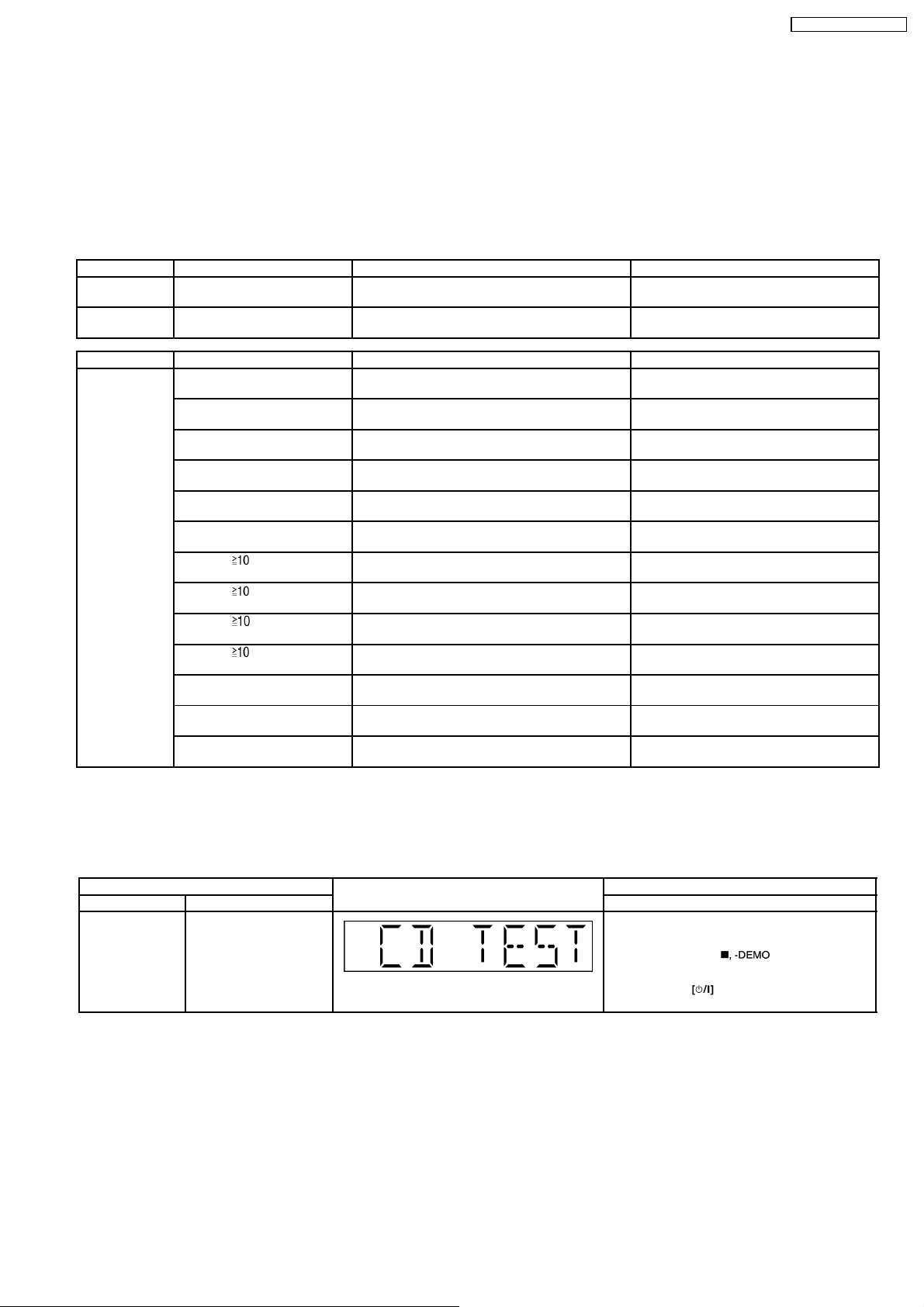
8.2.1. Service Mode Table 1
Item FL Display Key Operation
Mode Name Description Front Key
Self -Diagnostic
Mode
To enter into self
diagnostic checking for
main unit.
1. Select [CD] for DISC mode (Ensure no disc
2. Press and hold [
To exit, press
remote control.
is inserted).
]button for 2
seconds follow by [H.BASS].
button on main unit or
13
Page 14
SA-PMX2E / SA-PMX2EG
Item FL Display Key Operation
Mode Name Description Front Key
Doctor Mode To enter into Doctor
Mode for checking of
various items and
displaying EEPROM and
firmware version.
Note: The microprocessor version as
shown is an example. It
will be revise when there
is an updates.
FL Display
sequenceDisplay 1 → 2
(a) If there is NO EEPROM header string
OR
(b) If there is no EEPROM ( no date is
received by micro-processor) [NO] is
displayed.
(Display 1)
Checksum : (Condition 1)
Checksum : (Condition 2)
In any mode:
1. Press [
by [4] and [7] on remote control.
To exit Doctor Mode, press
main unit or remote control.
] button on main unit follow
button on
If the version of the EEPROM does not
match or not working properly [NG] is
display.
Checksum : (Condition 3)
If the EEPROM version matches, checksum
[YYYY] is displayed.
(Display 2)
The Check Sum of EEPROM and firmware
version will be display for 2 sec.
8.2.2. Service Mode Table 2
Item FL Display Key Operation
Mode Name Description Front Key
FL Display Test To check the FL
Tuner Check To Inspect Tuner Check
CD Open Test
Mode
segments display (All
segments will light up)
(For more information,
refer to section 8.2.3)
To check on the CD
Open function.
In doctor mode:
1. Press [DIMMER] button on remote control.
To cancel, press [0] button on remote control.
To exit Doctor Mode, press [ENTER] button on
remote control or
remote control.
In doctor mode:
1. Press [MUSIC PORT] button on remote
To exit Doctor Mode, press
main unit or remote control.
In doctor mode:
1. Press [6] button on remote control.
To exit Doctor Mode, press [ENTER] button on
remote control or
remote control.
button on main unit or
control.
button on
button on main unit or
14
Page 15
Item FL Display Key Operation
Mode Name Description Front Key
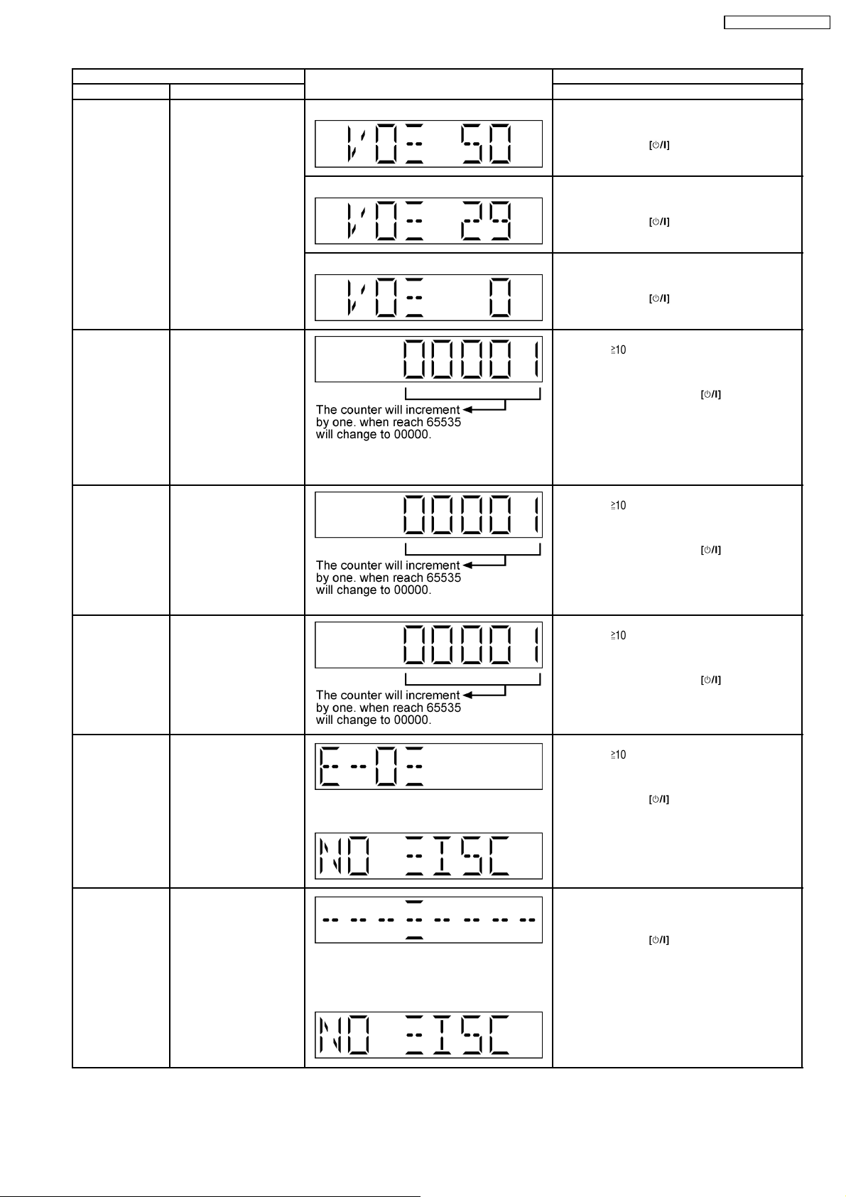
Volume Setting
Mode
To check for the volume
setting of the main unit.
The volume will be
automatically set to its
respective level (in dB).
Display 1 In doctor mode:
1. Press [7] button on remote control.
To exit Doctor Mode, press [ENTER] button on
remote control or
remote control.
During this mode,
treble/bass/EQ will be set
to ‘0’dB & OFF.
Display 1 In doctor mode:
2. Press [8] button on remote control.
To exit Doctor Mode, press [ENTER] button on
remote control or
remote control.
SA-PMX2E / SA-PMX2EG
button on main unit or
button on main unit or
CD Loading Test
Mode
CD Traverse Unit
Test Mode
CD Combination
Test Mode
To determine the
reliability of CD Loading
Unit.
To check for the
open/close operation for
the CD loading unit. It
fails when there is
abnormality in opening or
closing.
(For more information,
refer to section 8.2.4)
To check for the traverse
unit operation. In this
mode, the first & lost
track is access & read
(TOC). It fails when TOC
is not completed by IDS
or the traverse is out of
focus.
(For more information,
refer to section 8.2.5)
A combination of CD
loading & Traverse unit
test.
(For more information,
refer to section 8.2.6)
Display 1 In doctor mode:
3. Press [9] button on remote control.
To exit Doctor Mode, press [ENTER] button on
remote control or
remote control.
In doctor Mode:
1. Press [
control.
To cancel, press [0] button on remote control.
To exit Doctor Mode, press
main unit or remote control.
In doctor Mode:
1. Press [
control.
To cancel, press [0] button on remote control.
To exit Doctor Mode, press
main unit or remote control.
In doctor Mode:
1. Press [
control.
To cancel, press [0] button on remote control.
To exit Doctor Mode, press
main unit or remote control.
button on main unit or
], [1] & [1] button on remote
button on
], [1] & [2] button on remote
button on
], [1] & [3] button on remote
button on
CD Auto
Adjustment
Display
To display result of selfadjustment for CD.
(For more information,
refer to section 8.2.7)
Cold Start To activate cold start
upon next AC power up.
The [NO DISC] display will appear after 3 sec.
Note: This test do not work when selector is in
Tuner.
The [NO DISC] display will appear after 3 sec.
In doctor mode:
1. Press [
], [1] & [4] button on remote
control.
To exit Doctor Mode, press [ENTER] button on
remote control or
button on main unit or
remote control.
In doctor mode:
1. Press [SLEEP] button on remote control.
To exit Doctor Mode, press [ENTER] button on
remote control or
button on main unit or
remote control.
15
Page 16
SA-PMX2E / SA-PMX2EG
Item FL Display Key Operation
Mode Name Description Front Key
MP3 Test To Inspect MP3 disc
check.
(For more information,
refer to section 8.2.8)
USB Test To Inspect USB check.
(For more information,
refer to section 8.2.9)
In doctor mode:
1. Press [PROGRAM] button on remote
control.
To exit Doctor Mode, press [ENTER] button on
remote control or
remote control.
In doctor mode:
1. Select [USB] for USB mode (Ensure USB
device is inserted).
2. Press [2] button on remote control.
To exit Doctor Mode, press [ENTER] button on
remote control or
remote control.
8.2.3. Tuner Check
Purpose : Tuner inspection mode.
Below is the procedures for this mode.
Step 1: Enter into Doctor mode (For more information refer to section 8.1 on key operation to enter into this mode).
Step 2 : Press [TUNER] button on remote control.
· The system is switched to tuner inspection mode.
· The receiving frequency is set to [87.50Mhz] (Fmin) this time.
Step 3 : When [PLAY MODE] key is pressed, Auto Scan shall start from Fmin in the direction of downward.
· Auto Scan shall be continued until auto stop is made by pressing [0] key.
· Auto Scan shall stop when auto stop is made. When [0] key is pressed again in this state (auto stop state).
· Auto scan shall also be available for AM. It is also in the direction of downward.
1. [1] key is pressed..........FM 87.50MHz (Fmin) is received.
2. [2] key is pressed..........FM 108.00MHz (Fmax) is received.
3. [3] key is pressed..........FM 98.10MHz (Frequency set by Signal Generator) is received.
4. [4] key is pressed..........FM 90.10MHz.
5. [5] key is pressed..........FM 106.10MHz.
6. [6] key is pressed..........AM 522kHz (Fmin) is received.
7. [7] key is pressed..........AM 1629kHz (Fmax) is received.
8. [8] key is pressed..........AM 999kHz is received.
9. [9] key is pressed..........AM 603kHz is received.
button on main unit or
button on main unit or
8.2.4. CD Loading Test
Purpose : CD Loading OPEN/CLOSE aging test.
Below is the procedures for this mode.
Step 1: Enter into Doctor mode. (For more information refer to section 8.1 on key operation to enter into this mode)
Step 2 : Switch to CD mode.
Step 3 : Press [
], [1] & [1] buttons on the remote control unit. The following operation shall be carry out as below :-
16
Page 17

Step 4 : The FL shall display as below :
SA-PMX2E / SA-PMX2EG
The aging process will stop when the following conditions happens (counter value remains):-
1. When during “OPEN” operation, the tray stays in “CLOSE” state. (After REST SW is OFF, the CD OPEN SW)
· Do the CLOSE operation; stop the aging test at CLOSE condition.
2. When during “CLOSE” operation, the trays stays in “OPEN” state. (After CLOSE operation, REST SW was not off in 4s.)
· Do the OPEN operation; stop the aging test at OPEN condition.
When key [0] is pressed, the current test shall be cancelled and returns to Doctor mode display. The count value shall be reset to
(00000).
During this test, FL shall display as normal and no
display on the FL.
8.2.5. CD Traverse Unit Test
Purpose : <CD Access Inner and Outer Disc aging test>. CD playab ility aging test.
Below is the procedures for this mode.
Step 1: Enter into Doctor mode. (For more information refer to section 8.1 on key operation to enter into this mode)
Step 2 : Switch to CD mode & insert test disc into unit.
Step 3 : Press [
], [1] & [2] buttons on the remote control. The following operation shall be carry out as below:-
17
Page 18
SA-PMX2E / SA-PMX2EG
Step 4 : The FL shall display as below :
The aging process will stop when the following conditions happens (counter value remains):-
1. When during “OPEN” operation, the tray stays in “CLOSE” state. (After REST SW is OFF, the CD OPEN SW)
· Do the CLOSE operation; stop the aging test at CLOSE condition.
2. When during “CLOSE” operation, the trays stays in “OPEN” state. (After CLOSE operation, REST SW was not off in 4s.)
· Do the OPEN operation; stop the aging test at OPEN condition.
Step 3 : Due to certain reasons, when the following condition happens, the aging will stop but the count value shall be maintained
:
· TOC incomplete after 10s.
· Tracks not able to access for more than 2s (out of focus).
When key [0] is pressed, the current test shall be cancelled and returns to Doctor mode display. The count value shall be reset to
(00000).
During this test, FL shall display as normal and no
display on the FL.
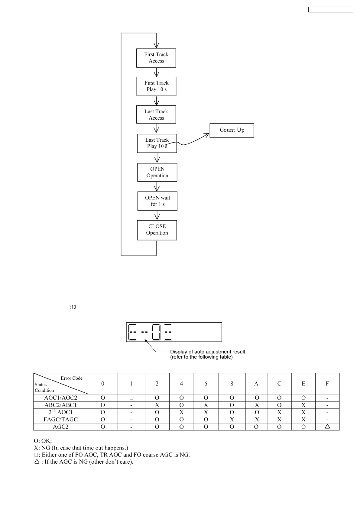
8.2.6. CD Combination Test
Purpose : This test is the combination of the CD loading & traverse unit test.
Below is the procedures for this mode.
Step 1: Enter into Doctor mode. (For more information refer to section 8.1 on key operation to enter into this mode)
Step 2 : Switch to CD mode & insert test disc into unit.
Step 3 : Press [
], [1] & [3] buttons on the remote control. The following operation shall be carry out as below:-
18
Page 19
SA-PMX2E / SA-PMX2EG
8.2.7. CD Auto Adjustment Display
Purpose : To display result of self-adjustment for CD.
Below is the procedures for this mode.
Step 1: Enter into Doctor mode. (For more information refer to section 8.1 on key operation to enter into this mode)
Step 2 : When [
correspond to the condition met as shown in the table below :
], [1] & [4] key are pressed at the doctor mode, the following shall be display ed for 3 secs. The result shall
19
Page 20
SA-PMX2E / SA-PMX2EG
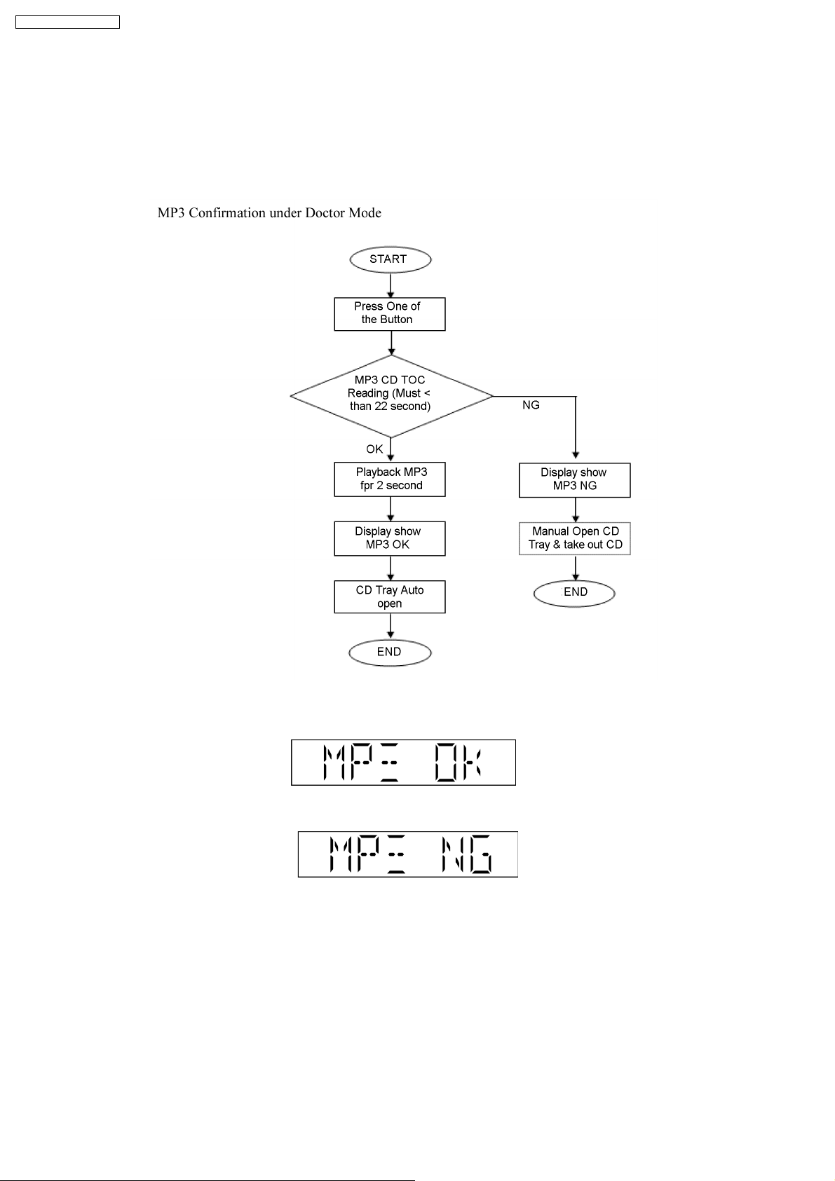
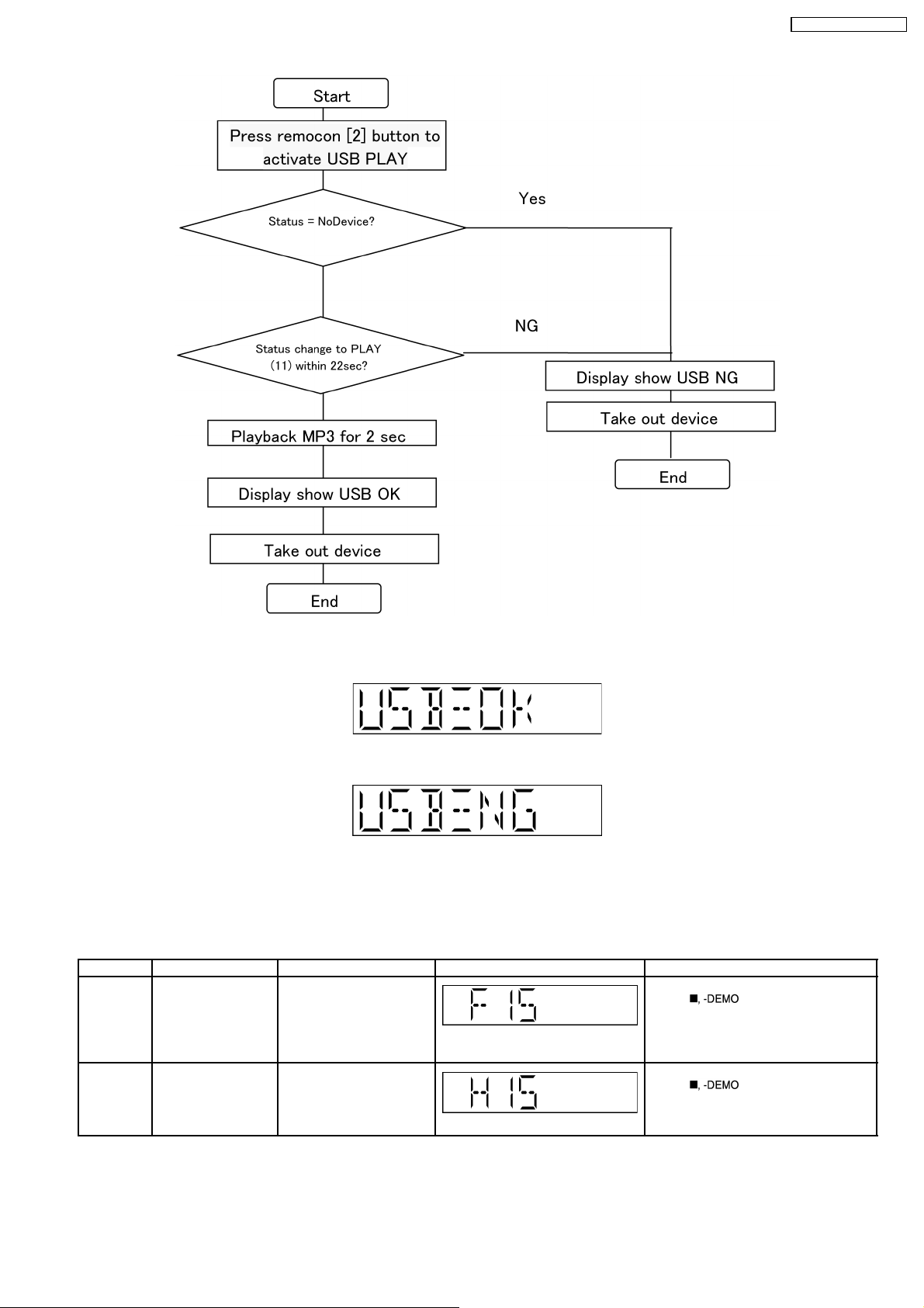
8.2.8. MP3 Test
Purpose : To check the MP3 Test.
Below is the procedures for this mode.
Step 1 : Enter into Doctor mode. (For more information refer to section 8.1 on key operation to enter into this mode)
Step 2 : Insert CD with MP3 tracks. (Ensure correct MP3 tracks is loaded)
Step 3 : Press [PROGRAM] button on remote control. Execute MP3 Disc Check (Refer Flowchart below)
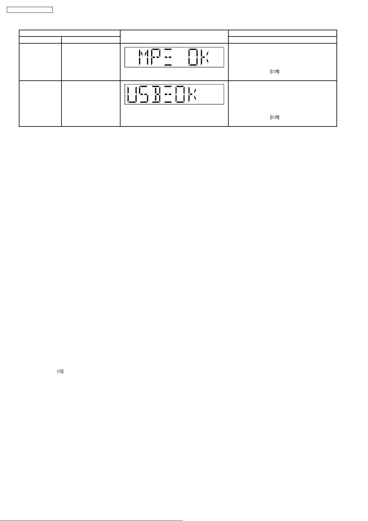
Result display :
· Displaye d if MP3 test OK
· Displaye d if MP3 test NG
8.2.9. USB Test
Purpose : To check the USB Test.
Below is the procedures for this mode.
Step 1 : Enter into Doctor mode. (For more information refer to section 8.1 on key operation to enter into this mode)
Step 2 : Insert USB devices with MP3 tracks loaded. (Ensure correct MP3 tracks is loaded)
Step 3 : Press [2] button on remote control. Execute MP3 USB Check (Refer Flowchart below)
20
Page 21
SA-PMX2E / SA-PMX2EG
Result display :
· Displaye d if USB test OK
· Displaye d if USB test NG
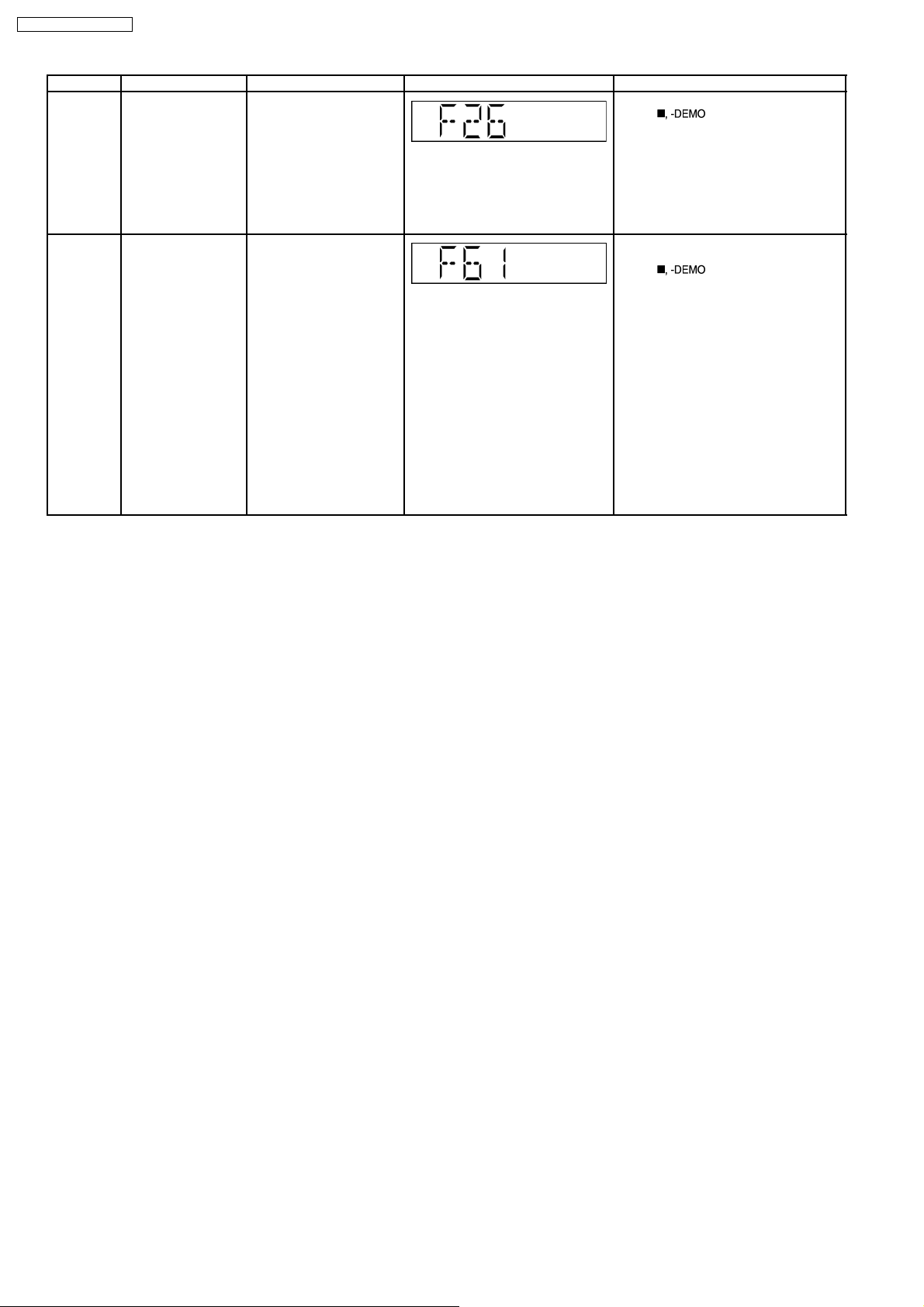
8.3. Error Code Table
Self-Diagnosis Function provides information on any problems occuring for the unit and its respective components by display ing
error codes. Thesed error code such as U**, H** and F** are stored in memory and held unless it is cleared.
The error code is automatically display after entering into self-diagnostic mode.
Error Code Diagnosis Contents Description of error Automatic FL Display Remarks
F15 CD REST SW
Abnormal
H15 CD Open SW
Abnormal
CD traverse position intial
setting operation failsafe
counter (1000 ms) waiting
for REST SW to turn on.
Error No. shall be clear by
force or during cold start.
During normal operation
CD OPEN SW On fail to
be detected with 4 sec.
Error No. shall be clear by
force or during cold start.
For CD unit (For Traverse).
Press [
error.
For CD unit (For Traverse).
Press [
error.
] on main unit for next
] on main unit for next
21
Page 22
SA-PMX2E / SA-PMX2EG
Error Code Diagnosis Contents Description of error Automatic FL Display Remarks
F26 Communication
between CD servo
LSI and micro-p
abnormal.
CD function DTMS
command, after system
setting, If SENSE = ´L´
cannot be detected.
Memory shall contain F26
code. After Power on, CD
function shall continue,
error display shall be "NO
DISC". Error No. shall be
clear by force or cold start.
F61 Power Amp IC output
abnormal
During normal operation, if
DCDET becomes "L",
normal POWER OFF
process shall not be
executed, PCONT shall be
switched to "L"
immediately. "GOODBYE"
shall not be display but the
error display F61 is
displayed instead. 2
seconds after the F61
displayed, ECONO shall be
set to "L" and FL display
shall be turned off. The
error content shall be
memorized when the
abnormality occurs and can
be display in the C-mecha
self-diagnostic mode
described later.
For CD unit (For Traverse).
Press [
] on main unit for next
error.
For Power Supply Related Error
Detection.
Press [
] on main unit for next
error.
22
Page 23
SA-PMX2E / SA-PMX2EG
9 Assembling and Disassembling
9.1. Caution
“ATTENTION SERVICER”
Some chassis components may be have sharp edges. Be careful when disassembling and servicing.
1. This section describes procedures for checking the operation of the major printed circuit boards and replacing the main
components.
2. For reassembly after operation checks or replacement, reverse the respective procedures.
Special reassembly procedures are described only when required.
3. Select items from the following index when checks or replacement are required.
Warning:
This product uses a laser diode. Refer to “Precaution of Laser Diode”.
ACHTUNG:
Die Lasereinheit nicht zerlegen.
Die Lasereinheit darf nur gegen eine vom Hertsteller spezifizierte Einheit ausgetauscht werden.
Below is the list of disassembly sections
· Disasse mbly of Top Panel Unit
· Disasse mbly of D-Port P.C.B
· Disasse mbly of USB P.C.B
· Disasse mbly of Front Panel
· Disasse mbly of Music Port P.C.B
· Disasse mbly of FL, Switch & Headphone P.C.B
· Disasse mbly of Rear Cabinet
· Disasse mbly of Main P.C.B
· Disasse mbly of Inner Chassis
· Disasse mbly of CD Mechanism Unit
· Disasse mbly of Transformer P.C.B
· Disasse mbly of Tuner Extent P.C.B
· Replacement of the Power IC
23
Page 24
SA-PMX2E / SA-PMX2EG
9.2. Disassembly flow chart
The following chart is the procedure for disassembling the casing and inside parts for internal inspection when carrying out the
servicing.
To assemble the unit, reverse the steps shown in the chart below.
24
Page 25
9.3. Main Parts Location Diagram
SA-PMX2E / SA-PMX2EG
25
Page 26
SA-PMX2E / SA-PMX2EG
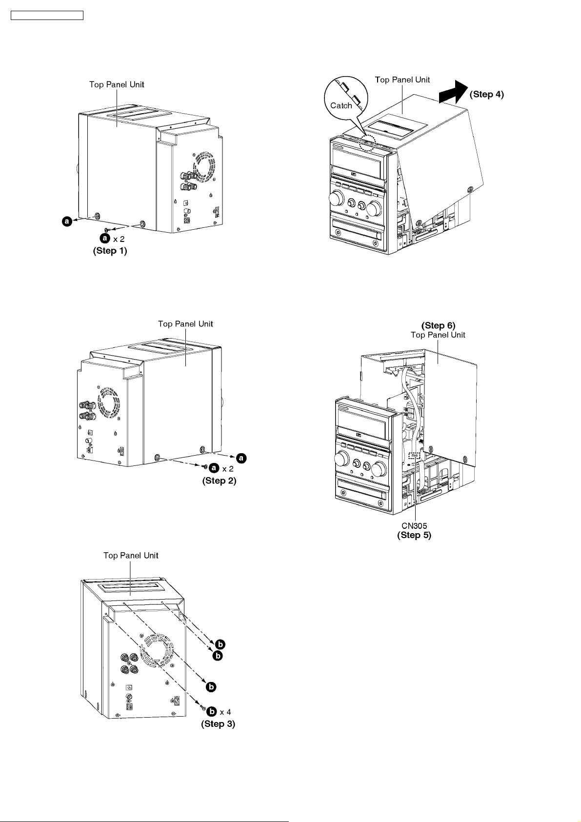
9.4. Disassembly of Top Panel Unit
Step 1 : Remove 2 screws.
Step 2 : Remove 2 screws.
Step 4 : Release the catch and lift the Top Panel Unit slightly
backward as arrow shown.
Step 3 : Remove 4 screws.
Step 5 : Detach FFC cable (CN305) on Main P.C.B.
Step 6 : Remove Top Panel Unit.
9.5. Disassembly of D-Port P.C.B
· Follow the (Step 1) - (Step 6) of Item 9.4.
26
Page 27
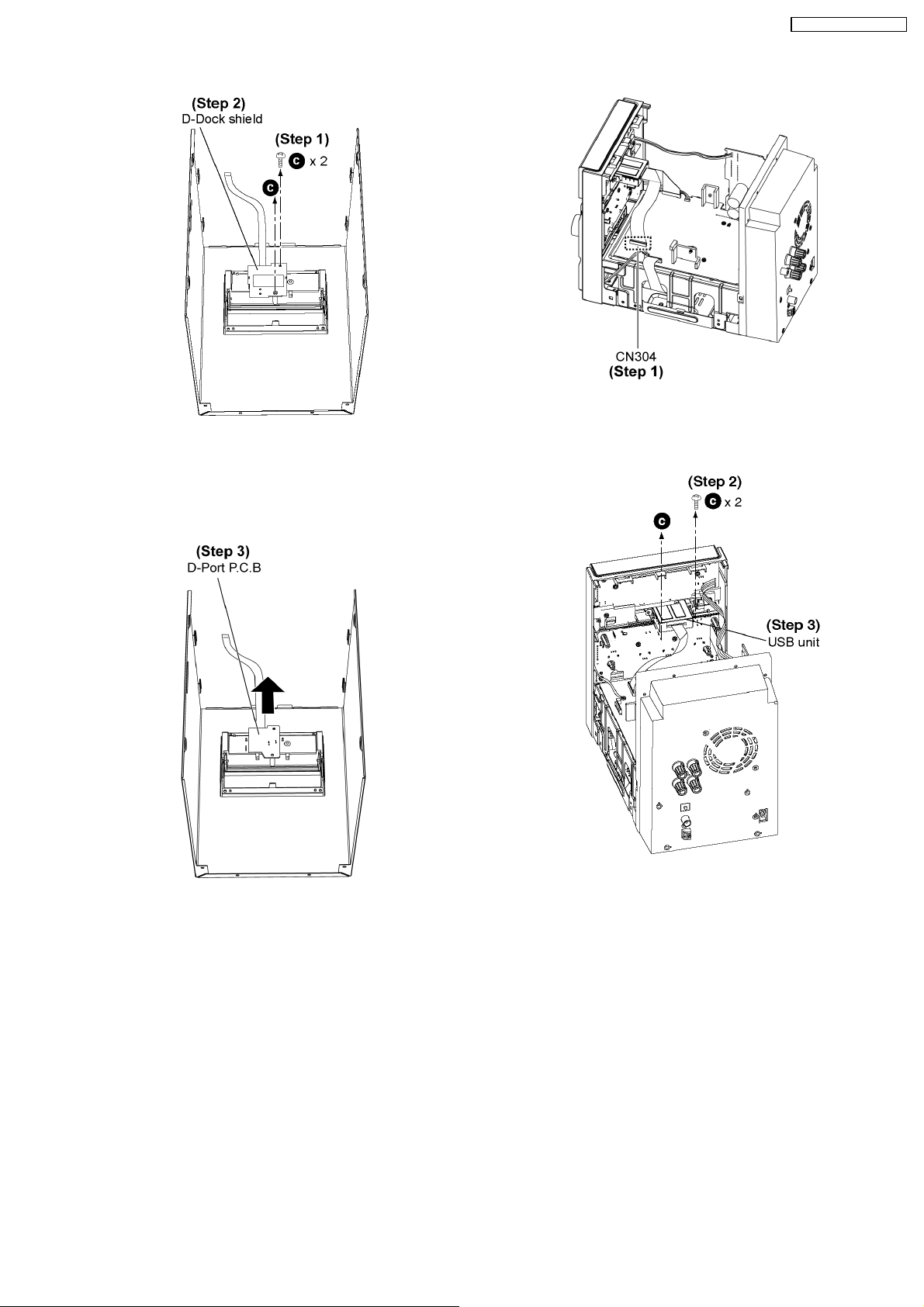
Step 1 : Remove 2 screws.
Step 2 : Remove D-Dock shield.
SA-PMX2E / SA-PMX2EG
Step 1 : Detach FFC cable (CN304) on Main P.C.B.
Step 3 : Remove D-Port P.C.B as arrow shown.
9.6. Disassembly of USB P.C.B
· Follow the (Step 1) - (Step 6) of Item 9.4.
Step 2 : Remove 2 screws.
Step 3 : Remove USB unit.
27
Page 28

SA-PMX2E / SA-PMX2EG
Step 4 : Remove USB bottom case as arrow shown.
Step 1 : Detach cable (CN304, CN600, CN801 and CN803) on
Main P.C.B & Transformer P.C.B.
Step 2 : Remove 1 screw from Chassis Ground wire altogether.
Step 5 : Unsolder 4 points.
Step 6 : Remove USB P.C.B.
9.7. Disassembly of Front Panel
· Follow the (Step 1) - (Step 6) of Item 9.4.
Step 3 : Release 2 catches at both L & R side.
Step 4 : Releas e the catch at the bottom cabine t and remove
the front panel as arrow shown.
28
Page 29

9.8. Disassembly of Music Port
P.C.B
· Follow the (Step 1) - (Step 6) of Item 9.4.
· Follow the (Step 1) - (Step 4) of Item 9.7.
SA-PMX2E / SA-PMX2EG
Step 1 : Remove 1 screw and release 1 catch.
Step 2 : Remove Music Port P.C.B.
9.9. Disassembly of FL, Switch &
Headphone P.C.B
· Follow the (Step 1) - (Step 5) of Item 9.4.
· Follow the (Step 1) - (Step 4) of Item 9.7.
· Disassembly of FL P.C.B
Step 2 : Remove 2 screws.
Step 3 : Remove the Cass Lid unit as arrow shown.
Step 4 : Remove 4 screws.
Step 5 : Remove FL P.C.B as arrow shown.
Step 1 : Flip down Cass Lid as arrow shown.
· Disassembly of Switch P.C.B
29
Page 30

SA-PMX2E / SA-PMX2EG
Step 6 : Remove all Knob and 2 Nuts.
Step 7 : Remove 4 screws and release 3 catches to remove
Switch P.C.B.
· Remove Headphone P.C.B
Step 1 : Detach cable (CN550) on Main P.C.B.
Step 2 : Remove 7 screws.
Step 3 : Remove Rear Cabinet as arrow shown.
Step 8 : Remove 2 screws and release 1 catch to remove
Headphone P.C.B.
9.10. Disassembly of Rear Cabinet
· Follow the (Step 1) - (Step 6) of Item 9.4.
9.11. Disassembly of Main P.C.B
· Follow the (Step 1) - (Step 6) of Item 9.4.
· Follow the (Step 1) - (Step 4) of Item 9.7.
· Follow the (Step 1) - (Step 3) of Item 9.10.
30
Page 31

SA-PMX2E / SA-PMX2EG
Step 1 : Detach cable (CN301, CN303, CN601) on Main P.C.B
& Transformer P.C.B.
Step 2 : Detach cable (CD open switch - S780).
Step 1 : Detach cable (CN301, CN303, CN601) and CD open
sw (S780).
Step 2 : Remove 5 screws.
Step 3 : Remove Main P.C.B. as arrow shown (Be careful of the
catch).
9.12. Disassembly of Inner Chassis
· Follow the (Step 1) - (Step 6) of Item 9.4.
· Follow the (Step 1) - (Step 4) of Item 9.7.
· Follow the (Step 1) - (Step 3) of Item 9.10.
Step 3 : Release 3 catches and remove the Inner Chassis as
arrow shown.
9.13. Disassembly of CD
Mechanism Unit
· Follow the (Step 1) - (Step 6) of Item 9.4.
· Follow the (Step 1) - (Step 4) of Item 9.7.
· Follow the (Step 1) - (Step 3) of Item 9.10.
· Follow the (Step 1) - (Step 3) of Item 9.12.
Step 1 : Remove 4 screws and CD Mechanism unit as arrow
31
Page 32

SA-PMX2E / SA-PMX2EG
shown.
9.14. Disassembly of Transformer
P.C.B.
· Follow the (Step 1) - (Step 6) of Item 9.4.
· Follow the (Step 1) - (Step 4) of Item 9.7.
· Follow the (Step 1) - (Step 3) of Item 9.10.
· Follow the (Step 1) - (Step 3) of Item 9.12.
Step 1 : Remove 1 screw.
Step 2 : Remove Tuner Extent P.C.B. as arrow shown (Be
careful of the catch).
Step 1 : Remove 4 screws.
Step 2 : Remove Transformer P.C.B. as arrow shown.
9.15. Disassembly of Tuner Extent
P.C.B.
· Follow the (Step 1) - (Step 6) of Item 9.4.
· Follow the (Step 1) - (Step 4) of Item 9.7.
· Follow the (Step 1) - (Step 3) of Item 9.10.
· Follow the (Step 1) - (Step 3) of Item 9.12.
9.16. Replacement of the Power IC
· Follow the (Step 1) - (Step 6) of Item 9.4.
· Follow the (Step 1) - (Step 4) of Item 9.7.
· Follow the (Step 1) - (Step 3) of Item 9.10.
· Follow the (Step 1) - (Step 3) of Item 9.11.
Step 1 : Remove 1 screws & Transistor Holder (For IC700).
Step 1 : Remove 1 screws (For IC500).
32
Page 33

Step 2 : Unsold er the terminal to replace the component.
Note: For replacement of regulator IC repeat step 1 & 2
9.17. Disassembly of Traverse Unit,
Driving Gear, and Cam Gear
SA-PMX2E / SA-PMX2EG
9.17.1. Disassembly of the Traverse Unit
· Follow the (Step 1) - (Step 6) of Item 9.4.
· Follow the (Step 1) - (Step 4) of Item 9.7.
· Follow the (Step 1) - (Step 3) of Item 9.10.
· Follow the (Step 1) - (Step 3) of Item 9.12 .
· Follow the (Step 1) of Item 9.13.
· Disasse mbly of gears drive
33
Page 34

SA-PMX2E / SA-PMX2EG
34
Page 35

SA-PMX2E / SA-PMX2EG
9.17.2. Disassembly of CD Servo P.C.B
· Follow the (Step 1) - (Step 6) of Item 9.4.
· Follow the (Step 1) - (Step 4) of Item 9.7.
· Follow the (Step 1) - (Step 3) of Item 9.10.
35
Page 36

SA-PMX2E / SA-PMX2EG
· Follow the (Step 1) - (Step 3) of Item 9.12 .
· Follow the (Step 1) of Item 9.13.
· Follow the (Step 1) - (Step 4) of Item 9.17.1.
9.17.3. Disassembly of Traverse Gear A
and Traverse Gear B
· Follow the (Step 1) - (Step 6) of Item 9.4.
· Follow the (Step 1) - (Step 4) of Item 9.7.
· Follow the (Step 1) - (Step 3) of Item 9.10.
· Follow the (Step 1) - (Step 3) of Item 9.12 .
· Follow the (Step 1) of Item 9.13.
· Follow the (Step 1) - (Step 4) of Item 9.17.1.
36
Page 37

10 Service Positions
Note: For description of the disassembly procedures, see the Section 9.
10.1. Check and Repair of Transformer P.C.B.
SA-PMX2E / SA-PMX2EG
37
Page 38

SA-PMX2E / SA-PMX2EG
10.2. Check and Repair of D-Port P.C.B.
38
Page 39

SA-PMX2E / SA-PMX2EG
10.3. Check and Repair of FL, Switch, Headphone and Music Port P.C.B.
39
Page 40

SA-PMX2E / SA-PMX2EG
10.4. Check and Repair of Main P.C.B.
40
Page 41

SA-PMX2E / SA-PMX2EG
10.5. Checking and Repairing of CD Servo P.C.B.
Note: Connect AC power cord and switch on the set. Eject tray loading, load in CD and switch off the set. Proceed with
checking
41
Page 42

SA-PMX2E / SA-PMX2EG
10.6. Check and Repair of USB P.C.B (Side B).
42
Page 43

CD SERVO P.C.B
Ref No. IC7001
MODE 1234567891011121314151617181920
CD PLAY 0000000000000000001.53.3
STANDBY 00000000000000000000.3
Ref No. IC7001
MODE 21 22 23 24 25 26 27 28 29 30 31 32 33 34 35 36 37 38 39 40
CD PLAY 1.6 0 1.5 1.5 1.7 0 3.3 3. 3 3. 2 0 0 1.6 1.6 1.6 0 0 0 1.7 1.8 1.8
STANDBY 0 0.1 0 0 0 0 0.2 0 0.2 0.2 0 0 0.2 0 0 0.2 0.2 0.2 0 0
Ref No. IC7001
MODE 41 42 43 44 45 46 47 48 49 50 51 52 53 54 55 56 57 58 59 60
CD PLAY 0.2 2.4 1.8 1.7 0 1.8 3.3 1.2 1.2 0 1.7 1.7 0.8 1.4 1.4 1.5 0 3 1.5 0
STANDBY 000.20.10.20.10.30.10.20.2000000.200.30.20
Ref No. IC7001
MODE 61 62 63 64 65 66 67 68 69 70 71 72 73 74 75 76 77 78 79 80
CD PLAY 3.3 0 0 0 0 0 0 2.8 2.8 2.7 0 2.6 0 1.6 0 1.5 3.3 0 3.3 1.7
STANDBY 0.1 0.1 0.1 0.1 0.1 0.1 0.1 0 0 0 0.2 0 0.2 0.2 0.2 0 0.3 0 0.3 0.2
Ref No. IC7001
MODE 81 82 83 84 85 86 87 88 89 90 91 92 93 94 95 96 97 98 99 100
CD PLAY 1.62.300 000000003.30000000
STANDBY0.30.200000000000.30000000
Ref No. IC7002
MODE 1234567891011121314151617181920
CD PLAY 1.601.60000007.44.23.43.53.42.94.13.73.47.40
STANDBY0.1000000000.30.10.10.10.10.10.100.100
Ref No. IC7002
MODE 21 22 23 24 25 26 27 28
CD PLAY 7.4 0 0 0 7.4 1. 6 1.6 1.6
STANDBY0.30000000
Ref No. Q7601
MODE E C B
CD PLAY 3.1 2 2.4
STANDBY 0.3 0.1 0.3
SA-PMX2E/EG CD SERVO P.C.B
SA-PMX2E / SA-PMX2EG
11 Voltage Measurement & Waveform Chart
Note:
· Indicated voltage values are the standard values for the unit measured by the DC electronic circuit tester (high-impedance)
with the chassis taken as standard.
Therefore, there may exist some errors in the voltage values, depending on the internal impedance of the DC circuit tester.
· Circuit voltage and waveform described herein shall be regarded as reference information when probing defect point
because it may differ from actual measuring value due to difference of Measuring instrument and its measuring condition
and product itself.
11.1. Voltage Measurement
11.1.1. CD SERVO P.C.B
43
Page 44

SA-PMX2E / SA-PMX2EG
11.1.2. MAIN P.C.B
Ref No. IC200
MODE 1 2 3 4 5 6 7 8 9 10 11 12 13 14 15 16 17 18 19 20
CD PLAY 4.3 4.3 4.3 4.3 4.3 4.3 4.3 4.3 4.3 4.3 4.3 4.3 0 4.3 4.3 4.3 4.3 4.3 4.3 4.3
STANDBY 0.3 0.3 0.3 0.3 0.3 0.3 0.3 0.3 0.3 0.3 0.3 0.3 0 0 0.3 0.3 0.3 0.3 0.3 0.3
Ref No. IC200
MODE 21 22 23 24 25 26 27 28 29 30 31 32 33 34 35 36 37 38 39 40
CD PLAY 4.3 4.3 4.3 4.3 4.3 4.3 4.3 0 0 4.3 4. 3 4.3 4.3 4.3 4.3 4.3 4.3 8.6 0 0
STANDBY 0.3 0.3 0.3 0.3 0.3 0.3 0.3 0 0 0 0.1 0.1 0.1 0.1 0.2 0.3 0.2 0 0 0
Ref No. IC200
MODE 41 42 43 44 45 46 47 48 49 50 51 52 53 54 55 56
CD PLAY 0 4.3 4.3 4.3 4.3 4.3 4.3 4.3 4.3 4.3 4.3 4.3 4.3 4.3 4.3 4.3
STANDBY 0 0.1 0.2 0.2 0.2 0 0.1 0.1 0.1 0.3 0.3 0.3 0.1 0.3 0 0.1
Ref No. IC201
MODE 1 2345678
CD PLAY -9 0 0 0 0 0 0 9
STANDBY 0 00-10000
Ref No. IC300
MODE 1 2 3 4 5 6 7 8 9 10 11 12 13 14 15 16
CD PLAY 0 1.4 1.6 1.6 3.3 0 1.6 1.6 0 0 0 3.3 1.6 1.7 0 1.6
STANDBY 0 0.3 0 0 0.3 0 0.2 0.1 0 0 0 0 0.2 0.1 0 0
Ref No. IC301
MODE 12345
CD PLAY 3.3 0 1.3 0 0
STANDBY 3.3 3.3 0 1.6 0
Ref No. IC302
MODE 1 2345678
CD PLAY 5.2 5.2 5.2 0 5.2 5.2 5.2 9.6
STANDBY 5.2 5.2 5.2 0 5.2 5.2 5.2 9.6
Ref No. IC500
MODE 12345
CD PLAY 7.5 16.1 0 9.6 16
STANDBY 7.5 16.2 0 9.5 16.2
Ref No. IC501
MODE 12345
CD PLAY 3.3 11 0 5.6 2.7
STANDBY 3.3 11 0 5.6 2.7
Ref No. IC502
MODE 1234
CD PLAY 11 0 0 0
STANDBY 1.1 0 0 0
Ref No. IC700
MODE 1 2 3 4 5 6 7 8 9 10 11 12 13 14 15 16 17 18 19 20
CD PLAY -26. 2 0 0 27.7 0 -28. 4 -20.8 28.1 10.8 -0.3 -28.7 -16.3 -28.8 -0.3 10.8 28.1 -28.4 -28.4 0 27.7
STANDBY 0.1 0 0 0.1 0 0.1 0.4 0.1 0.5 0.2 0.1 0.1 0.1 0.2 0 0.1 0.1 0.1 0 0.1
Ref No. IC700
MODE 21 22 23
CD PLAY 0 0 4.7
STANDBY 0 0 0.1
Ref No. IC800
MODE 1 2 3 4 5 6 7 8 9 10 11 12 13 14 15 16 17 18 19 20
CD PLAY 0 3.2 3.2 3.2 3.2 0 0 0 0 1.3 0. 7 3.2 1.6 0 1.5 3.2 3.2 3.2 0 1.8
STANDBY 0 0 0 0 0 0 0 0 0 0 0.7 3.3 1.7 0 1.6 3.3 3.3 3.2 0.1 1.9
Ref No. IC800
MODE 21 22 23 24 25 26 27 28 29 30 31 32 33 34 35 36 37 38 39 40
CD PLAY 0000.2000000000000003.23.2
STANDBY3.30000000000000000000
Ref No. IC800
MODE 41 42 43 44 45 46 47 48 49 50 51 52 53 54 55 56 57 58 59 60
CD PLAY 03.23.200003.23.100000001.51.603
STANDBY 000000000003.80.10000000
MAIN P.C.B
44
Page 45

PANEL P.C.B
Ref No. IC900
MODE 1234567891011121314151617181920
CD PLAY 0 0 0 0 1.9 3.3 2.2 2.8 2. 2 0.2 0.2 0 2.9 -23.6 -23.6 -23.6 -17.1 -23.6 -23.6 -19.1
STANDBY 0 0 0 0 0 0.3 0.1 0 0 0.2 0.2 0 0.3 0 0 0 0 0 0 0
Ref No. IC900
MODE 21 22 23 24 25 26 27 28 29 30 31 32 33 34 35 36 37 38 39 40
CD PLAY -25.8 -25.8 -23.6 -19.1 -25.8 -25.8 -25.8 -25.8 -19.2 -26.3 -17.1 -23.6 -23.6 -23.5 -23.5 -23.5 -23.5 -23.5 -23.5 -23.5
STANDBY 00000000000000000000
Ref No. IC900
MODE 41 42 43 44
CD PLAY -23.5 -23.5 3.3 0
STANDBY 0 0 0.3 0
SA-PMX2E/EG PANEL P.C.B
SA-PMX2E / SA-PMX2EG
Ref No. IC800
MODE 61 62 63 64 65 66 67 68 69 70 71 72 73 74 75 76 77 78 79 80
CD PLAY 03.20.1030000000000003.203.2
STANDBY 03.30.10000000.30.30000003.300
Ref No. IC800
MODE 81 82 83 84 85 86 87 88 89 90 91 92 93 94 95 96 97 98 99 100
CD PLAY 3.2 3. 2 0 0 0 0 1.4 1.8 3 3.2 3. 2 0 0 3.2 3.2 0 1.9 3.3 3.2 3.2
STANDBY 0.7 3.3 0 2.2 0 0 1.4 1.8 0 0 3.3 0 3.3 3.3 1.4 0 0 0 3.3 3.3
Ref No. IC801
MODE 1 2 3
CD PLAY 0 0 0
STANDBY 0 0 0
Ref No. IC802
MODE 1 2345678
CD PLAY 0 3.3 0 0 1.5 1.1 0 0
STANDBY 0 3.2 0 0 0 0 0 0
Ref No. Q200 Q201 Q202 Q203 Q204
MODE E C B E C B E C B E C B E C B
CD PLAY 0 0 -5.7 0 0 -5.7 0 0 -5.7 0 0 -5.7 0 0 -5.7
STANDBY 0 0 0.7 0 0 0.7 0 0 0.7 0 0 0.7 0 0 0.7
Ref No. Q210 Q211 Q330 Q331 Q332
MODE E C B E C B E C B E C B E C B
CD PLAY 0 -6.2 0 0 0 -5.7 3.2 0 3.1 0 3.2 0 0 1.2 0
STANDBY 2.2 2.3 0 0 0 0.7 3.2 0 3.1 0 3.2 0 0 0 0
Ref No. Q333 Q334 Q335 Q336 Q337
MODE E C B E C B E C B E C B E C B
CD PLAY 0 1.5 0 0 1 0 0 1.2 0 0 1.3 0 0 1.3 0
STANDBY 00.10 00.10 00.10 00.10 00.10
Ref No. Q500 Q501 Q502 Q503 Q504
MODE E C B E C B E C B E C B E C B
CD PLAY -0.6 -9 0 -8.5 -28. 1 -9 0 3.2 0 0 3.2 0 10 16.2 10.2
STANDBY 0.4 0.1 0 0 0.1 0.1 0 0 0.2 0.2 0.4 0 0.4 0.2 0.2
Ref No. Q505 Q506 Q550 Q551 Q552
MODE E C B E C B E C B E C B E C B
CD PLAY 0 3.2 -3.2 2.4 3.2 0 0 0.2 0.2 10 0 10 0 10 0
STANDBY 0 0.6 0.1 0 0.6 0 0 0 0 0.4 0 0.4 0 0.4 0
Ref No. Q553 Q700 Q701 Q702 Q703
MODE E C B E C B E C B E C B E C B
CD PLAY 0 3.2 0 3.3 3.3 0 -28.4 -28.4 -27.7 0 4.7 0 -28.6 -25.1 -28.2
STANDBY 0 0.6 0 0.3 -4.5 0 0.2 0.2 -3.9 0 0 3 0 0 0
Ref No. Q704 Q800 Q803
MODE E C B E C B E C B
CD PLAY 3.3 -27.7 3.2 0 0 0 3.2 -0.1 2.8
STANDBY 0.6 0 3.2 0 0 0 3.2 3.2 0.4
SA-PMX2E/EG MAIN P.C.B
11.1.3. PANEL P.C.B
45
Page 46

SA-PMX2E / SA-PMX2EG
11.1.4. USB P.C.B
Ref No. IC900
MODE 1234567891011121314151617181920
CD PLAY
STANDBY 0000000.600.60.60000000000
Ref No. IC900
MODE 21 22 23 24 25 26 27 28 29 30 31 32 33 34 35 36 37 38 39 40
CD PLAY
STANDBY 000000000000.100000000
Ref No. IC900
MODE 41 42 43 44 45 46 47 48 49 50 51 52 53 54 55 56 57 58 59 60
CD PLAY
STANDBY
Ref No. IC900
MODE 61 62 63 64
CD PLAY
STANDBY
Ref No. IC951
MODE 12345678
CD PLAY
STANDBY
USB P.C.B
1.3 3.2 3.2 0 0 0 3.2 3.2 3.2 1.8 0 1.5
3.3 3.3 3.3 1.4 1.4 1.3 1.3 1.3 1.3 1.3 1.3 1.3 1.3 1.3 1.3 1.3 1.3
1.4 1.2 1.8 0 1.4 3.2 3.2 0.1 3.2 0 0 1.2
000000000000
0 1.8 1.4 3.2
00.60 0
0 5 5 3.2 3.3 0.5 0.5 0.5
0000.60000
0000
0.1 0 1.4 3.1 3.1 3.1 0 1.3
00000000
SA-PMX2E/EG USB P.C.B
3.3 1.4 0
11.1.5. TRANSFORMER P.C.B
TRANSFORMER P.C.B
Ref No. Q600 Q601 Q602 Q603 Q604
MODE E C B E C B E C B E C B E C B
CD PLAY 0 11. 6 0 6.2 7. 7 6. 9 0 1.8 1.8 -26.3 -36.6 -26.9 -4.2 -23.1 -4.8
STANDBY 0 0 0.6 11.6 12.5 12.3 0 1.8 2.5 0 0 -0.4 -0.6 -0.1 0
Ref No. Q605 Q606 Q607 Q608
MODE E C B E C B E C B E C B
CD PLAY -48.9 -45.6 -48.2 13.2 31 13.1 -49 -28.5 -45.9 27.9 45.3 31.1
STANDBY -0.3 0 -0.3 2.8 0 0.2 -0.1 0.2 0 0.1 0.1 0
SA-PMX2E/EG TRANSFORMER P.C.B
11.1.6. SWITCH P.C.B
SWITCH P.C.B
Ref No. Q903
MODE E C B
CD PLAY 0 0 0.8
STANDBY 0 0 0
SA-PMX2E/EG
SWITCH P.C.B
46
Page 47

11.2. Waveform Chart
SA-PMX2E / SA-PMX2EG
CN301 PIN 2
CD PLAY
2.04Vp-p (50usec.div)
CN301 PIN 17
CD PLAY
3.44Vp-p (10msec.div)
CN304 PIN 11
CD PLAY
3.55Vp-p (10msec.div)
CN301 PIN 4
CD PLAY
2.06Vp-p (50usec.div)
CN301 PIN 18
CD PLAY
3.60Vp-p (10msec.div)
CN801 PIN 7
CD PLAY
3.48Vp-p (10msec.div)
CN301 PIN 15
CD PLAY
3.52Vp-p (5msec.div)
CN301 PIN 19
CD PLAY
3.64Vp-p (10msec.div)
CN801 PIN 8
CD PLAY
3.36Vp-p (10msec.div)
CN301 PIN 16
CD PLAY
3.76Vp-p (10msec.div)
CN304 PIN 10
CD PLAY
3.62Vp-p (10msec.div)
CN801 PIN 9
CD PLAY
3.48Vp-p (10msec.div)
IC800 PIN 10
CD PLAY
748mVp-p (50usec.div)
IC800 PIN 19
CD PLAY
3.48Vp-p (10msec.div)
IC800 PIN 11
CD PLAY
1.70Vp-p (10usec.div)
IC800 PIN 26
CD PLAY
3.44Vp-p (10msec.div)
IC800 PIN 13
CD PLAY
3.20Vp-p (50nsec.div)
IC800 PIN 58
CD PLAY
3.40Vp-p (2.5msec.div)
47
IC800 PIN 15
CD PLAY
2.32mVp-p (50nsec.div)
Page 48

SA-PMX2E / SA-PMX2EG
48
Page 49

12 Wiring Connection Diagram
B
TUNER EXTENT P.C.B
SA-PMX2E / SA-PMX2EG
22 . . . . . . . . . . . . 2
21 . . . . . . . . . . . . 1
22 . . . . . . . . . . . . 2
21 . . . . . . . . . . . . 1
CN304
CP300
12
CN301
CD OPEN SW
C
CN801
1 . . . . . . . . . . . . 23
2 . . . . . . . . . . 22
I
TRANSFORMER P.C.B
CN803
3 2 1
CN305
1
2
.
.
.
.
.
.
.
.
.
.
.
.
12
13
MAIN P.C.B
CN600
1
.
.
4
12
.
.
.
.
.
.
.
.
.
.
1
CN601
WH500
12 . . . . . . . . . . . 1
FAN UNIT
1 . . . . . . . .9
CN303
CN550
2
1
SOLDER SIDE
D
MUSIC PORT P.C.B
JK970
PbF
JK700
WH910B
SOLDER SIDE
PbF
3
.
1
MUSIC PORT
SPEAKER
WH901A
10
.
.
.
.
.
.
.
.
1
PbF
WH901B/JW901
10
.
.
.
.
.
.
1
WH911A/JW9
6
.
.
.
.
.
1
VR900
F
PANEL P.C.B
G
SWITCH P.C.B
VR902
SOLDER SIDE
VR901
SOLDER SIDE
Z900
SENSOR
VR903
TUNE_JOGBASSTREBLEVOLUME
WH900
CN900
1
.
.
4
23
PbF
9 . . . . . . . . 1
WH303
Z300
10 . . . . . . . . . 1
PbF
SOLDER SIDE
Tuner Pack
J
22
.
.
.
.
.
.
.
.
.
.
.
.
.
2
1
HEADPHONE P.C.B
SOLDER SIDE
WH911B
6
.
.
.
.
JK980
1
PbF
HEADPHONE
AC IN
230V 50Hz
(SUB-TRANSFORMER)
(POWER-TRANSFORMER)
JK600
T600
T601
CAUTION
RISK OF ELECTRIC SHOCK
AC VOLTAGE LINE.
PLEASE DO NOT TOUCH THIS P.C.B
SOLDER SIDE
PbF
13. . . . . . . . . . .1
CN806A
CN2401
24 . . . . . 2
23 . . . . . 1
PbF
SOLDER SIDE
OPTION V.1 (TO DOCK)
E
D-PORT P.C.B
H
USB P.C.B
P901
1
2
.
.
.
.
.
.
.
.
.
.
.
.
.
.
.
.
.
.
.
.
.
21
.
22
(SIDE B)
49
SOLDER SIDE
P903
6
4
.
.
.
.
1
5
PbF
USB
CN7002
22
21
.
.
.
.
.
.
.
.
.
.
.
.
.
.
.
.
.
.
.
.
.
.
2
1
A
CD SERVO P.C.B
SOLDER SIDE
PbF
.
16
CN7001
1
2
.
.
.
.
.
.
.
.
.
.
.
.
.
.
15
OPTICAL PICKUP
Page 50

SA-PMX2E / SA-PMX2EG
50
Page 51

13 Block Diagram
13.1. CD SERVO/ OPTICAL PICKUP UNIT
SA-PMX2E / SA-PMX2EG
X7201
OPTICAL PICKUP
PHOTO DETECTOR
EE EE
D C
A B
D C
EFEF
SEMICONDUCTOR
LASER
B
FOCUS
COIL
TRACKING
COIL
[81]X1
[80]X2
CP701
CP1902
3
CP701
CP1902
7
CP1902
CP701
9
CP701
CP1902
2
CP701
CP1902
11
CP701
CP1902
4
IC7002
BA5948FPE2
4CH DRIVE
10,19,25
PVCC1
PVCC2
VCC
26
VREF
CP701
CP701
CP701
CP701
CP1902
16
CP1902
15
CP1902
14
CP1902
13
D3-
15
[CH3]
D3+
16
D4-
17
[CH4]
18
D4+
LEVEL
SHIFT
LEVEL
SHIFT
28
IN3
27
IN4
F+
F-
T+
T-
<+7.5V>
<+VREF>
Q7601
SWITCH
B
<CD_3.3V>
B
B
<+VREF>
B
[35]E
[40]A
[39]C
[38]B
[37]D
[36]F
[41]PD
[42]LD
[34]VREF
[25]FOP
[24]TRP
IC7001
MN6627954MA
SERVO PROCESSOR/
DIGITAL SIGNAL PROCESSOR/
DIGITAL FILTER D/A CONVERTER
[20]PRAMVDD15
[27]IODD2
[47]AVDD2
[77]IODD1
[79]REGON
[82]NTEST
[59]OUTR
[56]OUTL
[64]EXT2
[63]EXT1
[62]EXT0
[67]MCLK
[68]MDATA
[69]MLD
[72]RST
[70]STAT
[71]BLKCK
B
<3.3V>
CD RIGHT CH
CD LEFT CH
S7201
RESET SWITCH
CN7002
CN7002
CN7002
CN7002
CN7002
CN7002
CN7002
CN7002
16,15
8,7,6,3
CN807
19
CN807
21
CN807
CN807
17
CN807
CN807
5,4
CN807
2
CN807
1
TO MAIN
BLOCK DIAGRAM 2/2
TO MAIN
BLOCK DIAGRAM 1/2
OPTICAL PICKUP P.C.B
M7301
TRAVERSE
MOTOR
M7302
SPINDLE
MOTOR
D2+
14
M
M
[CH2]
13
D2-
D1+
12
[CH1]
D1-
11
LEVEL
SHIFT
LEVEL
SHIFT
MUTE
[CH1]
MUTE
[CH2]
1
IN2
3
IN1
4
PC1
PC2
2
[23]TRVP
[21]SPOUT
[22]PC
CD SERVO P.C.B
SA-PMX2E/EG CD SERVO/ OPTICAL PICKUP UNIT BLOCK DIAGRAM
51
Page 52

SA-PMX2E / SA-PMX2EG
13.2. MAIN(1/2)/ TUNER EXTENT/ PANEL/ SWITCH/ HEADPHONE/ D-PORT
TO TRANSFORMER
BLOCK DIAGRAM
TO CD SERVO
BLOCK DIAGRAM
TO USB MODULE
BLOCK DIAGRAM
WH500
CN601
12
WH500
CN601
10
CN7002
CN301
15,16,17,208,7,6,3
CN7002
CN301
18,195,4
CN7002
CN301
1
CN7002
CN301
CN301
CN7002
CN301
CN7002
CD OPEN SWITCH
P901
CN304
8,10
P901
CN304
7
CN304
P901
5,6,12,15
P901
CN304
13
CN304
P901
4,17,18,20
CN304
P901
1,9,19
[49]PCONT
[20]HALT
[2]TU_TUNED
[3]TU_ST
[4]TU_CLK
[5]TU_SDA
4
1,2,3,5
WH303CN303
Z300
TUNER PACK
TUNER EXTENT P.C.B
Q800
+3.3V
<VREF>
4
2
22
212
617
7,816,15
CP300
1
3
4
<CD_STAT>
4
3
RESET
SWITCH
D805
D804
[12]/RESET
[42]CD_MDATA
[43]CD_MLD
[39]CD_MCLK
[80]CD-RST
[48]CD_STAT
[19]BLKCK
[92]OPEN_H
[91]CLOSE_L
[82]REST_SW
[78]CD_OPEN_SW
[38]USB_RST
[34]USB_REQ
[30]USB_DAT
[29]USB_CLK
[65]USB_MMOD
[55]VERR
[56]TERR
IC800
C2CBYY000422
MICROPROCESSOR
[52]D_NRST
[51]D_PON
[88]BASS_JOG
[84]TUNE_JOG
[46]FL_CLK
[47]FL_DATA
[59]RDS_CLK
[58]RDS_DATA
[37]DMPU_CLK
[36]DMPU_TX
[35]DMPU_RX
[53]D_MPUMOD
[45]D_PLLSDA
[44]D_PLLSCL
[54]D_MPUMOD
[50]D_NRFRESET
[1]F_HOP2
[7]F_HOP1
[81]DCDET
[28]DPORT_PCONT
[69]ASP_DATA
[68]ASP_CLK
[21]PCONT2
[40]MUTEA
[93]KEY1
[94]KEY2
[95]VOL_JOG
[87]TRE_JOG
[22]FL_RST
[23]FL_CS
[18]RMT
2
+3.3V
DPRT_PCONT
[5]Vdda
[12]Vddd
[2]RDDA
[16]RDCL
IC300
C1BB00001137
RDS IC
[6]Vssa
[11]Vssd
[14]XOUT
[13]XIN
4
2
4
X320
F_HOP1
F_HOP2
DC_DET
DOCK_RPB
DOCK_LPB
ASP_DATA
ASP_CLK
PCONT2
MUTEA
WH303 CN303
4
WH303
CN303
6
BLOCK DIAGRAM
TO MAIN(2/2)
CN900 CN801
9,10
16,17
CN900 CN801
11,12,13,14 12,13,14,15
CN900 CN801
1,2,3,12
CN900 CN801
10
CN302
16
CN302
18
CN302
6,7,8,9
CN302
3,4
CN302
1,2,5,11
CN300
CN300
CN300
CN300
CN300
S900-S909
KEY SW
+5.5V
<SYS5.5V>
VR900
VOLUME
JOG
4
D930
STANDBY LED
VR901
BASS
JOG
DAB EXTENT P.C.B
VR902
TREBLE
JOG
JK900W900
VR903
TUNE
JOG
WH901B WH901A
WH901B WH901A
EXTERNAL
ANT
DAB MODULE
24-23
GRID01~GRID11
4,5,6,7
10
TUNER_LEFT
TUNER_RIGHT
DAB_LEFT
DAB_RIGHT
FL900
FL DISPLAY
IC900
C0HBB0000057
FL DRIVER
[32]FL_DATA
[33]FL_CLK
[34]FL_CS
[35]FL_RESET
REMOTE SENSOR
92-41
SEG1~SEG17
[38]+VP
[37]CD3.3V
Z900
TO MAIN(2/2)
BLOCK DIAGRAM
FROM
TRANSFORMER
13
+VP
+3.3V
PANEL P.C.B
MAIN P.C.B
<Vref>
WH911A WH911B
WH911A
WH911A
+5.6V
SWITCH P.C.B
CN2401
8
CN2401
13
CN2401
CN2401
20
CN2401
12
CN2401
21
CN2401
17
CN2401
15
D-PORT P.C.B
2
WH911B
4
WH911B
1
CN307
D-PORT
RCH
HEADPHONE P.C.B
Q330
DETECT
SWITCH
DOCK
CN900 CN801
CN900 CN801
CN900
CN801
CN900
CN801
3.3V
<SYS3.3V>
3
1
4
22
Q331
DOCK
DETECT
SWITCH
Q930
LED
SWITCH
CN305 CN806A
13
CN305 CN806A
11
CN305 CN806A
222
CN305 CN806A
1
CN305 CN806A
4
CN305 CN306
3
CN305 CN806A
10
CN305 CN806A
5
3.3V
<SYS3.3V>
D933
TO MAIN(2/2)
BLOCK DIAGRAM
2
VCC
+B
GND
7
IC802
EEPROM
(NOT SUPPLIED)
[3]CS
[4]CLK
[6]DATA
[22]EE_CS/
[23]EE_CLK
1
[24]EE_DATA
[63]HP_SW
[60]KEY_LED
[57]ACK_IN
[25]IPOD_DET
[31]DPRT_RX
[32]DPRT_TX
4
3
OUT
GND
IC301
C0JBAB000884
LOGIC IC
VCC
IC302
DUAL OP-AMP
C0ABBB000297
5
+3.3V
<SYS3.3V>
1
INA
HP_LEFT
HP_RIGHT
Q332
REV
Q333
FWD
SWITCH
Q334
SWITCH
FSKIP
SWITCH
Q336
PAUSE
SWITCH
Q337
PLAY
SWITCH
Q335
RSKIP
SA-PMX2E/EG MAIN(1/2)/ TUNER EXTENT/ PANEL/ SWITCH/ HEADPHONE/ D-PORT BLOCK DIAGRAM
[10]Xcin
X801
[11]Xcout
[75]DPRT_REV
[74]DPRT_FWD
[73]DPRT_RSKIP
[72]DPRT_FSKIP
[71]DPRT_PAU
[70]DPRT_PLAY
Xout
Xin
]
]
31[
51[
X800
[66]D_LINKDET1
[67]D_LINKDET2
SWITCH
52
Page 53

13.3. MAIN(2/2)/ USB MODULE/ MUSIC PORT/ TRANSFORMER
TO MAIN(1/2)
BLOCK DIAGRAM
DAB_R
DAB_L
DAB RCH
DAB LCH
TO MAIN(1/2)
BLOCK DIAGRAM
F_HOP1
F_HOP2
SIGNAL LINES
: MAIN SIGNAL LINE
: FM/AM SIGNAL LINE
: USB SIGNAL LINE
:CD SIGNAL LINE
:CD DA SIGNAL LINE
SA-PMX2E / SA-PMX2EG
: AUX SIGNAL LINE
: IPOD SIGNAL LINE
TO MAIN(1/2)
BLOCK DIAGRAM
TO CD SERVO
BLOCK DIAGRAM
TO MAIN(1/2)
BLOCK DIAGRAM
P903
USB CONNECTOR
MAIN P.C.B
MUSIC PORT
[1]USB_VBUS
[2]D+
[3]D-
VSS
TUNER_LEFT
TUNER_RIGHT
DPRT_L
DPRT_R
CN7002
CN807
21
CN7002
CN807
19
ASP_DATA
ASP_CLK
JK970
HP_LEFT
HP_RIGHT
MUTEA
PCONT_2
DPRT_PCONT
2
4
IC951
C0DBZYE00002
VOLTAGE
REGULATOR
LCH
RCH
GND
1678
X900
WH910B
WH910B
MUSIC PORT P.C.B
2,3
VDD
[4]CTL
[5]FLAG
[50]VERR
[51]TERR
[15]MMOD0
[4]USBD[6]USBD+
[11]OSCI
CN803
1
CN803
3
<D5V>
USB CONTROLLER
[12]OSCO
IC900
MNZSFB5KJM1
CD SIGNAL LCH
CD SIGNAL RCH
Q204,
Q211
MUTING
SWITCH
3
[8]CD_NRST
[64]CD_MLD
[58]CD_DA
[55]CD_CLK
[57]CD_STAT
[48]I2C_DATA
[47]I2C_REQ
[46]I2C_CLK
[7]VDD
[9]VDD33
[17]VPP
[38]VDD33
[49]VDD5
[10]VDDI
[42]VDDI
[62]VDDI
[61]STIN
[58]TCLK
[54]STREQ
[14]NRST
Q202,
Q203
MUTING
SWITCH
P901
P901
B
<3.3V>
B
<D1.8V>
P901
2
P901
4
P901
P901
4
P901
USB MODULE P.C.B
<DPRT_5V>
1
4,14,22
16
13,15
8,11,17,18
10
3,5,6,19
+5V
+3.3V
+5.6V
CN802
CN802
BLOCK DIAGRAM
CN802
CN802
CN802
CN802
CN802
[5]IN_L3
[6]IN_R3
[9]IN_L5
[10]IN_R5
[11]IN_L6
[12]IN_R6
[39]CLOCK
[40]DATA
[1]IN_L1
[2]IN_R1
+3.3V
<SYS3.3V>
Q803
MUTING
SWITCH
IC502
4
Vctrl
C0DAZYY00017
5V
REGULATOR
2
Vout5V
GND
3
IC501
3.3V
1
C0DAZYY00005
VOLTAGE
REGULATOR
4
5.6V
CD_DGND
3
TO MAIN(1/2)
BLOCK DIAGRAM
TO MAIN(1/2)
TO MAIN(1/2)
BLOCK DIAGRAM
[7]IN_L4 [8]IN_R4
C1BB00001121
[37]R-OUT
Q210
SWITCH
Vin
1
Vctrl
1
2
VCC
<SUB+B2>
DC_DET
IC200
ASP
+B
[42]L-OUT
+9.6V
9V
Q502,Q503
DC DET
SWITCH
[38]VCC
C0AABB000125
DUAL OP-AMP
IC801
C0CAABC00007
5.5V
REGULATOR
32
TO MAIN(1/2)
BLOCK DIAGRAM
Q505,Q506
DC DET
SWITCH
Q500
SWITCH
Q501
-9V
REGULATOR
IC201
1
+9.6V
JK700
SPEAKERS
Q201 Q200
MUTE
SWITCH
D800
VREF
VDD
D801
<PCONT>
<VCC+>
<VCC->
Q700,704
HOP
SWITCH
+3.3V
WH500
WH500
WH500
WH500
WH500
WH500
B
B
Q701,Q703
SWITCH
MUTE
SWITCH
CN601
10
CN601
12
CN601
11
CN601
8
CN601
1,2
CN601
5,6
[11]V
[13]V
[8]VDDP1
[16]VDDP2
[1]OSC
FILTER
FILTER
<SUB+B>
SUB+B2
SUB+B
VCC-
-VP
VCC+
[14]OUT2
1
P
S
S
2
P
S
S
IC700
C1AA00000755
POWER AMP IC
[10]OUT1
[5]STBY[22]IN2+[2]IN1+
D553D551
<SYS5.5V>
B
VOLTAGE
Z600
Q552
FAN
SWITCH
Q553
DC
DETECT
+9V
<FAN9V>
Q602
HALT
SWITCH
D613~D616
Q702
MODE
SWITCH
TO MAIN(1/2)
BLOCK DIAGRAM
Q504
FAN 9 V
REGULATOR
IC500
VCC
2
C0DAZYY00006
5
CTL
VOLTAGE
REGULATOR
GND
3
Q600
PCONT
SWITCH
DISPLAY
Q604,
Q605,
Q607
D609(DB)
D609(EB/EG)
FP603
FP602
Q603
-VP
B
REGULATOR
D640~D643
B
D604~D607
B
Q606,
Q608
VOLTAGE
B
REGULATOR
VOLTAGE
B
REGULATOR
TO FL
FP601
FP604
FP600
D600~D603
V01
4
V02
1
+7.5V
+9.6V
T601
RL600
MAIN TRANSFORMER
DC_DET
Q601
REGULATOR
TRANSFORMER
F1
Q551
FAN
CONTROL
Q550
FAN
DETECT
SWITCH
D618
SUB
T600
LEFT CHANNEL
RIGHT CHANNEL
+9V
<FAN9V>
L600
TRANSFORMER P.C.B
CN550
CN550
2
1
SA-PMX2E/EG MAIN(2/2)/ USB MODULE/ MUSIC PORT/ TRANSFORMER BLOCK DIAGRAM
JK600
AC INLET
TO FAN
53
Page 54

SA-PMX2E / SA-PMX2EG
54
Page 55

14 Notes of Schematic Diagram
(All schematic diagrams may be modified at any time with
the development of new technology)
Notes:
S900: POWER switch (AC IN
S901: CD switch (CD
S902: USB switch (USB
S903: OPTION switch (OPTION
S904: FM/AM switch (FM /AM /MUSIC P.).
S905: STOP/-DEMO switch (
S906: REW switch (ALBUM→).
S907: FF switch (←ALBUM).
S908: H.BASS switch (H.BASS).
S909: CD OPEN switch (
S7201: REST switch.
VR900: VR VOLUME jog.
VR901: VR BASS jog.
VR902: VR TREBLE jog.
VR903: VR TUNE jog.
/ ).
).
/ ).
).
/ -DEMO).
).
SA-PMX2E / SA-PMX2EG
· Importance safety notice :
Components identified by
characteristics important for safety.
Furthermore, special parts which have purposes of fireretardant (resistors), high-quality sound (capacitors), lownoise (resistors), etc. are used.
When replacing any of components, be sure to use only
manufacturer´s specified parts shown in the parts list.
· Capacitor values are in microfarad(µF) unless specifi ed
otherwise, F=Farad, pF=Pico-Farad
Resistance values are in ohm(Ω), unless specified
otherwise, 1K=1,000Ω, 1M=1,000KΩ
· Voltage and Signal lines:
: +B Signal line
: -B Signal line
: CD-DA signal line
: CD signal line
: Main signal line
: AUX signal line
: FM/AM signal line
: IPOD signal line
: USB signal line
mark have special
55
Page 56

SA-PMX2E / SA-PMX2EG
56
Page 57

SA-PMX2E / SA-PMX2EG
15 Schematic Diagram
15.1. CD SERVO CIRCUIT
1234567891011121314
A
SCHEMATIC DIAGRAM - 1
OPTICAL PICKUP CIRCUIT
CD SERVO CIRCUIT
: + B SIGNAL LINE
: CD DA SIGNAL LINE
: CD SIGNAL LINE
A
(FOR REFERENCE ONLY)
R7601
C7601
4.7
LASER DIODE
6
B
C
8
NBOUT
GND
NAOUT
VREF
C
8
7
6
5
C
10
11
12
13
14
15
C
16
11
12
4
9
10
5
2
3
C
GND
1
2
VCC
C
3
BIN
4
AIN
1
2
3
4
5
6
7
8
9
CN7001
VCC
LD GND
GND
GND (GUARD)
VREF
LPD
GND (GUARD)
W7025
1
0
2
F
3
E
4
LD
5
6
7
A
8
9
B
10
11
12
13
T-
14
T+
15
F-
16
F+
R7650
Q7601
5.6
C7613
B1ADCF000001
LASER POWER DRIVE
6.3V33
W7023
0.1
Q7601
C7670
0.1
0
D
E
GND1
D4-
D4+
D1-
D1+
W7027
+
SPINDLE MOTOR
191817 2015 16
0
PVCC2
PVCC1
TP
36
PGND2
PGND1
NC
NC
GND
IC7002
BA5948FPE2
4 CH DRIVE IC
GND
TP
C7335
0.1
C7334
10V220
39
D3-
D2+
14 12 911 1 013
+
TRAVERSE MOTOR
D3+
D2-
TP
38
TP
37
F
G
TP
22 233021 282724 25 26
NCNCNC
NC
NC
W7022 0 W7020 0 W7019 0 W7018 0
C7626
0.1
W7017
0
C7614
6.3V100
W7026
0
TP
28
VREF
0
W7016
W7024
0
90
R7327
1k
TRV GAIN
R7336
10
VCC
VREF
NC
PC1
IN1
R7335
100
C7352
0.018
FO GAIN
IN3
IN4
IN2
PC2
2167298345
R7349
R7329
C7338
0.056
R7323
3.3k
R7325
330
0
W7021
18k
1k
R7339
R7217
1k
C7225
1000P
C7226
R7253
10
W7003
W7002
1000P
0
0
50
49
48
47
46
45
44
43
42
40
39
38
37
36
35
34
33
32
31
30
29
28
27
26
C7218
0.082
C7241
1000P
R7212
820
DSLF
ARFIN
ARFDC
AVD D2
RFIN
RFOUT
RFENV
CENV
LD
PD
A
C
B
D
F
E
VREF
CTRCRS
OSCIN
AVS S2
SRVMON1
SRVMON0
DVDD1
IODD2
TRP
FOP
25
IREF
TRVP
23 21 20224124
R7221
100
C7231
6.3V220
W7005
0
C7230
0.1
PLLF
OUTL
PLLF0
AVS S1
AVD D1
[50] ARFFB
[49] ARFOUT
DIGITAL SIGNAL PROCESSOR/
DIGITAL FILTER D/A CONVERTER
[26] DVSS1
PC
PRAMVDD15
PRAMVDD33
SPOUT
PRAMVSS33
19 17 15 141618
10u
C7164
10u
C7165
R7332
1k
EXT1
EXT2
EXT0
OUTR
DVSS3
NSRVMONON
IC7001
MN6627954MA
SERVO PROCESSOR/
A0
A2
A1
A10
BA1
BA0
13
87TP 86
TP
TP
24
FLAG
A3
10 8 7912 11
TX
NRAS
MCLK
MDATA
DVDD2 [76]
IODD1 [77]
SDRCK [100]
NCAS
NWE
MLD
A4
1k
R7218
C7263
0.1
7471 7267 685655585752515453 65 6661 6259 60 6463 7069 73 75
NRST
SMCK
DQSYTXT
DVSS2
REGON
X2
X1
NTEST
D2
D1
D0
D3
D4
D5
D6
D7
D15
D14
DRVDD
D13
D12
D11
D10
D9
D8
A9
PMCK
A11
76
77
78
79
80
81
82
83
84
85
86
87
88
89
90
91
92
93
94
95
96
97
98
99
100
STAT
BLKCK
A6A8A7
A5
465 213
W7011
0
C7234
0.1
C7235
6.3V10
W7011
0.1
C7264
TP
51
(RF)
W7014
0
C7217
0.1
R7211
82k
C7244
R7315
3.3k
R7111
10k
R7330
5.6K
0.015
C7216
680P
C7161
0.1
W7015
0
C7102
0.47
TP
50
C7107
0.022
TP
88
TP
89
0.1C7154
10k
C7223
W7012
6.3V4R7
0
C7203
6.3V220
C7204
0.1
C7142
3300P
0
W7013
C7155 0.1
R7328
1k
0.018
C7339
C7315
0.47
R7331
22k
C7233
TP
TP
TP
TP
W7001
0
W7004
0
0.1
8
9
31
4
TP
14
W7010
0
W7009
0
W7008
0
W7006
0
C7232
6.3V220
R7214
X7201
H2B169500005
TP
13
470
TP
R7254
C7166
0.01
MAZ80560ML
LB7263 0
LB7262 0
W7007
7
TP
1K
REST SW
R7220
D7650
C7228
50V1
LB7264 0
0
TP
3
S7201
1M
2
TP
TP
18
C7227
50V1
TP
17
19
B
16
TP
C
CN7002
22
AGND
21
LCH OUT
20
AGND
19
W7029
C7243
0.1
TP
11
RCH OUT
18
DGND
17
ST_IN
0
16
ST_CLK
15
ST_REQ
14
3.3V
13
DGND
12
LD SW
11
TX
10
7.5V
9
PGND
8
MCLK
7
MDATA
6
MLD
5
BLKCK
4
STAT
3
RST
2
RESET_SW
1
LOADING
TP
10
C7253
470P
12
W7028
0
TP
1
TP
2
31
1
TO
MAIN CIRCUIT
(CN301) IN
SCHEMATIC
DIAGRAM - 2
22
D
E
F
G
H
SA-PMX2E/EG CD SERVO CIRCUIT
H
1234567891011121314
57
Page 58

SA-PMX2E / SA-PMX2EG
15.2. MAIN CIRCUIT
1 2345678910111213
H
G
F
E
D
C
B
SCHEMATIC DIAGRAM - 2
MAIN CIRCUIT
CN303
1
CL
2
SDA
3
TUNED
4
STEREO
DET_OUT
AFGND
CN304
D5V
DGND
USB_SCL
VERR
USB_REQ
USB_SDA
DGND
CD_CLK
DGND
CD_STAT
CD_DATA
DGND
STCLK
TERR
STREQ
STIN
CD_MLD
CD_RST
USB_RST
DGND
D3.3V
MMOD
LCH
RCH
+9V
5
6
7
8
9
1
2
3
4
5
6
7
8
9
10
11
12
13
14
15
16
17
18
19
20
C312 1000P
21
22
W104 0
TO
TUNER EXTENT
CIRCUIT (WH303)
IN SCHEMATIC
DIAGRAM - 7
TO
USB CIRCUIT
(P901) ON
SCHEMATIC
DIAGRAM - 10
C311
W103
DET_OUT
W1 0
0
SDA
TUNED
TU_L
TU_R
TGND
1000P
: +B SIGNAL LINE
CL
ST
9V
R370
4.7K
R371
4.7K
R372
4.7K
: -B SIGNAL LINE
TO
CD SERVO
CIRCUIT (CN7002)
ON SCHEMATIC
DIAGRAM - 1
: MAIN SIGNAL LINE
CN301
AGND
CD_L
AGND
CD_R
CD_DGND
ST_IN
ST_CLK
ST_REQ
CD_3.3V
CD_DGND
LD_SW/CLDCK
TX
CD_7.5V
PGND
MCLK
MDATA
MLD
BLKCK
STAT US
CD_RST
REST_SW
LOADING
TO
D-PORT CIRCUIT
(CN806A) ON
SCHEMATIC
DIAGRAM - 7
1
2
C301
3
C302 1000P
4
5
6
7
8
9
10
11
12
13
14
15
16
17
18
19
20
21
22
: AUX/IPOD SIGNAL LINE
1000P
100R302
100
R303
100
R304
100
R305
100
R306
100
R316
CN305
DOCK_L
AGND
DOCK_R
DOCK_DET1
DOCK5VGND
DOCK5VGND
D_DOCK5V
D_DOCK5V
DOCK_DET2
UART_OUT
AD_CTRL
IPOD_DET
UART_IN
C303
1000P
C304
1000P
13
12
11
10
9
8
7
6
5
4
3
2
1
R344
L302
J0JKB0000020
3.3K
: CD SIGNAL LINE
Q338
2SD1819AOL
SWITCH
R345
33K
W109
0
: FM/AM SIGNAL LINE
DOCK_L
DPORTGND
DOCK_R
DOCK_DET1
GND
DPRT_5V
DOCK_DET2
AD_CTRL
IPOD_DET
TxD
RxD
SYS3.3V
CD_L
GND(AGND)
CD_R
3.3V
GND(CD_GND)
7.5V
GND(PGND)
CD_MCLK
CD_MDATA
CD_MLD
BLKCK
STAT
CD_RST
RESETSW
LOADING
AUX_L
AUX_R
TU_L
TU_R
DPRT_L
DPRT_R
CD_L
CD_R
R321
2.2K
R323
220
RDCL
RDS-ID
R324
1K
RST
RDDA
R322
R275
6.8K
R276
6.8K
R203
3.9K
R204
3.9K
R207
0
R208
0
X320
H0H433400002
XOUT
Vref
220
5.6K
R273
5.6K
R274
8.2K
R201
8.2K
R202
10K
R209
10K
R210
12K
R213
12K
R214
47P
47P
C326
C327
X320
XIN
IC300
C1BB00001137
RDS IC
MPXIN
470P
C321
C320
16V10
1K
R325
C281
C282
C201
C202
C205
C206
C207
C208
1000P
1000P
1000P
1000P
220P
220P
1000P
1000P
Vddd
Vdda
C324
1000P
C322
16V47
Vssd
Vssa
C325
16V47
1012141516 13 11
7561432
MODE
FLOUT
C323
560P
9
TEST
CIN
8
16V1
C27516V10
C27616V10
C211
C21216V1
C21516V1
C21616V1
C21716V10
C21816V10
B1
B2
B5
TO MAIN
SECTION (2/5)
1
GND
USB_VERR
USB_CLK
USB_RST
USB_DAT
BUSY
USB_5V
A
GND
USB_MMOD
USB_TERR
CD OPEN SW
(REF NO. 7)
CD_OPEN_SW
2
CD_OPEN_SW
RDS_CLK
RDS_RDY
W107
RDS_DATA
DET_OUT
3.3V
0
1
/
5
LB321
J0JBC0000015
GND
B6
SA-PMX2E/EG MAIN CIRCUIT
1 2345678910111213
58
Page 59

15 16 17 18 19 20 21 22 23 24 25 2614
SCHEMATIC DIAGRAM - 3
SA-PMX2E / SA-PMX2EG
MAIN CIRCUIT
1
C239
16V100
IN-L1
2
IN-R1
3
IN-L2
4
IN-R2
5
IN-L3
6
IN-R3
7
IN-L4
8
IN-R4
9
IN-L5
10
IN-R5
11
IN-L6
12
IN-R6
13
GND
14
REF-IN
15 16 17 1918
B1
B2
C240
16V100
B5
C219
50V1U
OP-OUT
IGVOUT-L
[15] REF_OUT
IGVOUT-R
REC-R
C220
50V1U
53 52 51 50 49 47 46 455556 54
REC-L
PREV-IN-R
PREV-IN-L
HBMIX-IN
C229
0.047
R223
100K
R271
0.047C235
SUR2
IC200
ASP IC
HBFLT-OUT
50V4.7uC230
C223
TRE-L
HARM-IN
D200
R224
R221 1.5K
SUR1
C1BB00001121
HBMIX-OUT
3.9K
2200P
MID-L1
MID-L2
[43] POSTV-IN-L[56] OP-IN
HARM-OUT
HBATT-IN
2420 2221 23 27 2825 26
C234
0.039
B0ACCK000005
18K
R225
5.6K
C225 0.022
BASS-L1
HBATT-OUT
C231
R219
1u
22KR226
: +B SIGNAL LINE
15K
C241
16V10
C227 0.022
4448 43
L-OUT
T-OUT-L
BASS-L2
NC
DATA
CLOCK
VCC
R-OUT
POSTV-IN-R
T-OUT-R
BASS-R2
BASS-R1
MID-R2
MID-R1
TRE-R
NC
HBLPF-IN1
HBLPF-OUT
NC
C232
50V0.47
100K
R227
: -B SIGNAL LINE
42
41
40
39
38
37
36
C242
16V10
35
C228
0.022
34
33
C226
0.022
32
31
C224
R272
2200P
30
29
0.1u
C233
3.9K
R220
15k
C236
0.1u
C200
16V100
4.7
R222
: MAIN SIGNAL LINE
C243
50V4.7
C238
220P
C237
220P
C244
50V4.7
R278
10K
: AUX/IPOD SIGNAL LINE
R267
560
R265
2.2k
C277
50V4.7
R268
560
C278
R266
50V4.7
2.2k
R277
10K
C283
4700P
C284
4700P
R263
C271
C272
R264
2.2K
0.39
0.39
2.2K
R297
R298
: CD SIGNAL LINE
R269
2.2k
100K
100K
R270
2.2k
C273
50V1
C274
50V1
: FM/AM SIGNAL LINE
C253
50V0.47
C251 1200P
R239 100K
C254
50V0.47
C252 1200P
R240 100K
C250
C255
0.01
0.01
R241
10K
C245
100P
675
C0AABB000125
OP-AMP IC
R242
10K
R279
180
R243
68K
C247
27P
IC201
C246
100P
C259
50V33u
USE_DGND
8
243
1
C248
27P
R244
68K
Q210
B1GDCFJJ0047
MUTING SWITCH
R228
100
R229
R230
27K
56K
C268
C257
16V10
C258
16V10
10V10
9V
Q200, Q201
B1ABGC000005
R245
MUTING SWITCH
4.7K
R251
R260
1K
R259
1K
100K
R249
100K
R250
Q203
Q204
4.7K
R252
4.7K
R247
R255
1.5K
R256
1.5K
1K
Q200
R248
1K
Q201
Q202, Q203, Q204, Q211
B1ABGC000005
HEADPHONE MUTING SWITCH
R257
22
Q202
Q211
R258
22
R295
47k
R296
47k
R246
4.7K
22
R254
22
R253
N
C269
3300P
C270
3300P
R261
R262
LEFT1
B7
RIGHT1
-9V
HP_L
3.3K
GND
3.3K
HP_R
TO MAIN
SECTION (1/5)
B6
W106
D204
DCDET
B0ACCK000005
9V
ASP_DATA
ASP_CLK
SYS3.3V
VREF-(GND)
DPRT_DET2
DPRT_DET1
Q332
DPRT_REV
R330
180K
R336
82K
R331
180K
Q333
DPRT_FWD
R332
220K
Q330
B1ADCE000012
DOCK_DET1
33K
Q334
DPRT_RSKP
R338
15K
DPRT_FSKP
Q335
R337
R334
220K
R339
10K
Q336
DPRT_PAU
R333
220K
R335
220K
Q331
B1ABEB000002
DOCK_DET2
R341
R340
5.6K
6.8K
Q337
DPRT_PLAY
R342
10K
ACK_IN
Q332-Q337
B1GBCFGN0016
SWITCH
IC301
INANC GND
IC301
LOGIC IC
45
312
VCC OUT
C0JBAB000884
R343
100
AD_CTRL
DOCK_DET2
IC302
C0ABBB000297
DUAL OP AMP IC
DPRT_L
DPRT_R
DOCK_DET1
C330
C333
0
C345
33P
R363
R364
C344
100P
33K
675
8
1
C346
10V100
C337
10
W114
1
IC302
243
1
C339
R355
100P
33K
0
C338
33p
2
/
5
R356
6.8K
R357
10K
R362
6.8K
6.8K
C343
10
C340
R360 10K
10
C341
10
R358
6.8K
SA-PMX2E/EG MAIN CIRCUIT
MUTE_A
R365
1K
DOCK_R
R366
1.2K
AGND(GND)
DPORTGND
DOCK_L
TO MAIN
SECTION (3/5)
9.6V
B8
15 16 17 18 19 20 21 22 23 24 25 2614
59
Page 60

SA-PMX2E / SA-PMX2EG
SCHEMATIC DIAGRAM - 4
MAIN CIRCUIT
B7
PCONT2
9.6V
3.3V
F_HOP1
F_HOP2
RIGHT1
VDD
28 29 30 31 32 33 34 35 36 37 38 3927
Q704
R721
120K
R705
10
L704
J0JKB0000020
Q700
R701
120K
R722
Q703
R704
4.7k
: -B SIGNAL LINE
: +B SIGNAL LINE : MAIN SIGNAL LINE
Q700, Q704
B1GDCFGG0026
SWITCH
R700
120k
C728
Q701
0.1
82k
R702
27k
C703
1000P
Q701, Q703
B1ABGC000005
SWITCH
IN1-
IN1+
OSC
1 2 3 4 5 6 7 8 9 1011121314151617181920212223
C700
R709
0.47
5.6k
C702
330P
C701
R710
0.47
5.6k
VDDA1
C704
C706
VSSA1
C707
220P
C708
PROT
VDDP1
C710
220P
0.1
0.1
C709
SGND1
C705
0.1
0.1
0.1
BOOT1
C711
0.015
R711
10
C733
220P
OUT1
C712
0.1
IC700
C1AA00000755
POWER AMPLIFIER IC
STABI
VSSP1
0.1
C713
VSSP2
C714
10K
R716
IN2-
IN2+
OUT2
BOOT2
C715
0.015
0.1
R712
10
C716
220P
C717
220P
VDDP2
C718
VSSD
VSSA2
C720
0.1
0.1
0.1
C719
SGND2
C721
0.1
C722
0.1
VDDA2
R713
C723
5.6k
0.47
C726
330P
C725
1000P
R714
C724
5.6k
0.47
MODE
R715
100
C727
1000P
C741
16V10
5.6k
R718
12K
R717
B1GBCFJJ0051
Q702
SWITCH
LEFT1
VSS
C735
C734
0.1
0.1
L703
J0JKB0000020
R706
10
C737
C738
35V470
35V470
R708
4.7k
HEATSINK
C744
330P
L702
G0C220Z00002
1
RIGHT
22
R720
C742
C743
1000P
0.015
C736
0.015
LEFT
JK700
1
RIGHT
2
RIGHT_GND
3
LEFT_GND
4
LEFT
5
GND
1
Z700
2
3
VDD
SPEAKERS
B9
TO MAIN
SECTION (4/5)
C729
0.68u
43
2
C730
0.68u
C732
C731
R719
0.1
0.1
22
TO MAIN
B8
SECTION (2/5)
3
/
5
SA-PMX2E/EG MAIN CIRCUIT
B10
28 29 30 31 32 33 34 35 36 37 38 3927
60
Page 61

41 42 43 44 45 46 47 48 49 50 51 5240
SCHEMATIC DIAGRAM - 5
MAIN CIRCUIT
DCDET
T_PCONT
DPRT_5V
9.6V
-9V
D512 D514
9.6V
D512
B0ACCK000005
USB_5V
D510, D511, D513
B0ACCK000005
D510
7.5V
5.6V
C519
0.1
3.3V
C515
10V22
PCONT
CD_GND
DAB_GND
VREF-
DGND
B9
VDD
SYS5.5V
HALT
PCONT
AGND
HP_GND
D514
B0ACCK000005
D503
B0JAME000025
D513
24
VCC
5.6V
IC501
GND3.3V
V_CTRL
135
C514
0.1
Vctrl
IC502
Vin
142
6.3V100
3
GND
Vout5V
C522
C521
6.3V100
C520
16V3300
: -B SIGNAL LINE
: +B SIGNAL LINE
IC502
C0DAZYY00017
5V REGULATOR
C507
50V3.3U
D511
FAN9V
W119
0
Q504
B1AAJC000019
9V REGULATOR
IC501
C0DAZYY00005
DUAL REGULATOR IC
24
VO2VCC
IC500
C0DAZYY00006
DUAL REGULATOR IC
V01 GND CTL
135
C505
16V22
Q504
C511
0.01
C512
50V33
D501
B0BC01000014
R511
220
C506
16V470
R512
2.2
C508
16V470
Q502
C504
16V10
R507
47K
C513
25V3300
GND
Q503
R506
47K
R502
R503
560
2.7K
R504
2.7K
C503
R505
0.01
3.3K
Q501
B1BCCG000023
FUNCTION
W113
0
Q502, Q503
B1ABCF000174
FUNCTION
Q500
B1ACCF000094
FUNCTION
C502
50V10
Q500
R50015R501
27
3
2
1
4
SA-PMX2E / SA-PMX2EG
R510
R509
150K
68K
R518
33K
R508
22K
Q506
C509
Q505, Q506
B1ABCF000174
C516
50V1
R516
27K
6.3V100
FUNCTION
W112
0
R517
33K
C510
1000P
R515
27K
Q505
C517
50V1
R513
8.2K
D553
W116
0
GND
Q553
DCDET
B1ABCF000174
R514
8.2K
D551, D553
B0ACCK000005
D551
C552
Q553
SWITCH
C554
10V220
50V2.2
R561 820K
B1ABCF000174
R554
820K
R560
10K
0.1
C550
R557 56K
Q552
SWITCH
Q552
R550
R551
5.6K
Q551
B1ACKD000006
SWTICH
4.7K
10K
R552
C553 16V33
D550
B0ADCJ000020
R553
10K
3
R559
100
Q550
B1ABCF000174
SWITCH
56K
R558
2
1
R556
56K
C551
6.3V100
R555
18
CN550
FAN2(-)
1
2
C500
35V1000
C501
35V1000
W117
0
7
5
6
9108
12
11
W118
0
FAN1(+)
TO FAN
TO MAIN
SECTION (5/5)
TO MAIN
SECTION (3/5)
B10
VCC+
WH500
VCC+
VCC-
AGND
AGND
TO
TRANSFORMER CIRCUIT
(CN601) ON SCHEMATIC
DIAGRAM - 11
SUB+B GND
SUB+B
SUB+B2
HALT
PCONT
SYS5.5V
4
/
SA-PMX2E/EG MAIN CIRCUIT
5
B11
VCC-
41 42 43 44 45 46 47 48 49 50 51 5240
61
Page 62

SA-PMX2E / SA-PMX2EG
54 55 56 57 58 59 60 61 62 63 64 6553
SCHEMATIC DIAGRAM - 6
MAIN CIRCUIT
CN803
AUX_L
AGND
AUX_R
CN801
DGND
SYS5.5V
LED_CTRL
SYS3.3V
FL_CLK&CE
FL_DATA
FL_CS
FL_RST
TUNE_JOG
VOL_JOG
BASS_JOG
TRE_JOG
VREF-
HP_SW
HP_GND
5.6V
3.3V
RMT
KEY1
KEY2
GND
HP_L
HP_R
1
2
3
TO
MUSIC PORT
CIRCUIT (WH910B)
IN SCHEMATIC
DIAGRAM - 7
TO
SWITCH CIRCUIT
(CN900) IN
SCHEMATIC
DIAGRAM - 9
TO MAIN
SECTION (4/5)
(23)
(1)
: -B SIGNAL LINE
: +B SIGNAL LINE : MAIN SIGNAL LINE
Z701
321
R876
47K
R877
47K
R863
10K
RESETSW
C826
C823
560P
TUNE_JOG
TRE_JOG
BASS_JOG
LOADING
KEY2
KEY1
VOL_JOG
1
2
3
4
5
6
7
8
9
10
11
12
13
14
15
16
17
18
19
20
21
22
23
SYS3.3V
560P
R850
100
R858 100
R859 100
D804 B0ACCK000005
D805 B0ACCK000005
R860 100
R862 100
R861 100
R864 10K
R865 10K
C829
6.3V100
560P
C821
C819 560P
C817 560P
R884
15K
R887
R855 100
R866 100
R867 100
C818 560P
15K
C816
0.1
DCDET
R885 10K
R886 10K
R800 15K
R801 15K
R802 15K
R803 15K
C828
56P
: AUX SIGNAL LINE
CD_RST
80
CD_RST
F_HOP2
1
CD_OPEN_SW
787677
79
NC
CD_OPEN_SW
TU_TUNED
1K
R804
R853
1K
NC
TUNE_JOG
NC
NC
TRE_JOG
87 868889 8284 83 818590
BASS_JOG
NC
NC
CLOSE_L
OPEN_H
KEY2
KEY1
VOL_JOG1
AVss
REG SETTING
Vref
98 9495 92 919397 96
AVDD
99
100
DPRT_REV
R869
10K
NC
NC
[81]DCDET
[82]/RESETSW
[100] DEMO SELECTOR
TU_SCK
TU_ST
TU_SDA
342
5
X801
H0A327200111
DPRT_FWD
75
74
DPRT_REV
DPRT_FWD
FHOP1
NC
768
330K
R805
X801
22P
C801
C802 18P
DPRT_FSKP
DPRT_RSKP
737172
DPRT_FSKP
DPRT_RSKP
CNVSS
BYTE
9
C800 50V1
DPRT_PAU
DPRT_PAU
Xcin
10
4.7K
R806
100P
C803
ASP_DATA
DPRT_PLAY
R849 1K
69
70
ASP_DATA
DPRT_PLAY
/RESET
Xcout
12
11
0
R808
H2B100500004
ASP_CLK
DPRT_DET2
DPRT_DET1
R848 1K
R846 100
R845 100
67
68
ASP_CLK
DPRT_DET2
IC800
C2CBYY000422
MICROPROCESSOR
Vss
Xout
13
2
31
X800
USB_MMOD
R851
656466
USB_MMOD
DPRT_DET1
VCC
Xin
161415
C805
10K
Vss
/NMI
17
16V100
HP_SW
R847 100
C815
0.1
63
HP_SW
RMT
18
C804 0.1
R809 100
62
Vcc
BLKCK
19
R811
LED_CTRL
NC
HALT
20
R812 1K
R810 1K
1K
RDS_CLK
605961
KEY_LED
RDS_CLK
PCONT2
EE_CS/
22
21
R813 1K
R883 22K
ACK_IN
RDS_DATA
58
RDS_DATA
EE_CLK
23
R814 1K
R815 1K
USB_TERR
USB_VERR
55
57
56
TERR
VERR
ACK_IN
D_NRFRESET [50]
[32] DPRT_TX/RXD
[31] DPRT_RX/TXD
FL_CS
IPOD_DET
EE_DATA
262827
24
25
R816 100
R807 10K
542952
53
D_MPUMOD
D_MPUMOD
BUSY/USB_REQ
DPRT_PCONT
/FL_RST
R817 100
R822 100
51
D_PON
D_NRST
PCONT
STATUS
FL_DATA
FL_CLK&CE
D_PLLSDA
D_PLLSCL
MLD
MDATA
EPM
MUTE_A
MCLK
USB_RST
D_MPUCLK
D_MPUTX
D_MPURX
SCLK
USB_CLK
USB_DATA
R826 100
R825 100
30
4945 474641 4442 43 48 50
3937353231 3433 36 38 40
C808 220P
C809 220P
R839 1K
R838 100
R819 100
R818 100
R835 1K
R834 1K
R870 1K
R833 1K
R827 1K
R828 1K
R872
6.8K
Q800
R820
47K
85
NC
7
GND
6
R871
4.7K
C824
220P
C806
220P
B1GDCFGG0026
D0
D1
C807
220P
Q803
SWITCH
C0CAABC00007
5.5V REGULATOR IC
B1GBCFNN0009
D800, D801, D802, D803
B0ACCK000005
BACKUP_3.3V
D802
C810
50V1
D803
IC802
EEPROM IC
(NOT SUPPLIED)
IC801
Q800
SWITCH
NC
VCC
CS
CLK
R823
4.7K
R821
120
C811
10V1000
4321
D800
D801
R874
22K
R873
22K
VOUT VIN
C813
6.3V100
C825
0.022
2
GND
IC801
1
C814 0.01
EE_DATA
G
EE_CS
EE_CLK
W115
0
PCONT
STAT
FL_DATA
FL_CLK&CE
CD_MLD
CD_MDATA
EPM
SYS3.3V
CD_MCLK
MUTE_A
D_PLLSDA
BUSY
SCLK
RXD
TXD
F
E
D
C
3
VREF-
SYS5.5V
C812
10V220
B
H
ST
TUNED
B11
F_HOP2
SDA
CL
F_HOP1
RESET
RMT
BLKCK
HALT
PCONT2
EE_CS
EE_CLK
EE_DATA
FL_CS
IPOD_DET
FL_RST
USB_CLK
DPRT_PCONT
USB_DATA
5
/
SA-PMX2E/EG MAIN CIRCUIT
5
A
54 55 56 57 58 59 60 61 62 63 64 6553
62
Page 63

SA-PMX2E / SA-PMX2EG
15.3. TUNER EXTENT CIRCUIT, D-PORT CIRCUIT, MUSIC PORT CIRCUIT and HEADPHONE CIRCUIT
1234567891011121314
A
B
C
D
SCHEMATIC DIAGRAM - 7
TUNER EXTENT CIRCUIT
PORTSEL
1
CL
2
SDA
3
TUNED
4
LCH
Z300
ENG07825QF
TUNER PACK
5
STEREO
6
RCH
7
DET
8
TUNER_9V
9
C650
10
TNR_GND
0.1
WH303
CL
1
2
SDA
TUNED
3
4
LCH
STEREO
5
6
RCH
7
DET
8
TUNER_9V
TNR_GND
9
TO
MAIN CIRCUIT
(CN303) IN
SCHEMATIC
DIAGRAM - 2
: -B SIGNAL LINE
: +B SIGNAL LINE
: AUX/IPOD SIGNAL LINE
: FM/AM SIGNAL LINE
: MAIN SIGNAL LINE
MUSIC PORT CIRCUIT
JK970
5
4
2
MUSIC PORT
3
6
7
1
C972
R931
1.8K
C971
R930
1.8K
470P
470P
C970
C973
1000P
1000P
TO
MAIN CIRCUIT
(CN803)
IN SCHEMATIC
DIAGRAM - 6
WH910B
L930
J0JBC0000019
AUX_L
AGND
213
AUX_R
A
B
C
D
E
D-PORT CIRCUIT
C3001
0.1u
R3002
R3001
330K
220K
F
CN806A
DOCK_L
1
AGND
2
DOCK_R
3
DOCK5V
DOCK5V
AD_CTRL
IPOD_DET
UART_IN
4
5
6
7
8
9
10
11
12
13
WA3004
0
WA3003
0
DOCK_DET1
TO
MAIN CIRCUIT
(CN305) IN
G
SCHEMATIC
DIAGRAM - 2
DOCK5VGND
DOCK5VGND
DOCK_DET2
DOCK_UOUT
WA3002
0
WA3001
0
H
CN2401
BATT_GND
1
GND
2
(MIC_L) (RF Det)
3
NC
4
D-
5
DOCK_LIN
6
A_GND
7
DOCK_LOUT
8
V_GND
9
D+
10
VIDEO
11
DO_UART_OUT
12
DOCK_R OUT
13
(MIC_GND) (ANT) (ID_SET)
14
DOCK_DET2
15
DOCK_R IN
16
DOCK_DET1
17
(MIC_VCC) (RF_MUTE)
18
BATT2
19
DO_UART_IN
20
(A/D CONT) (RF_SEL)
21
IPOD_DET
22
DOCK5V
23
VBUS
24
OPTION V.1
(TO DOCK)
HEADPHONE CIRCUIT
TO
SWITCH CIRCUIT
(WH911A/JW9)
IN SCHEMATIC
DIAGRAM - 9
S909
WH911B
HP_SW
1
HP_L
243
HP_R
HP_GND
VREF-
5
KEY2_2
6
CD OPEN
R978
L980-L982
J0JBC0000019
L980
3.3K
L981
L982
SA-PMX2E/EG TUNER EXTENT / MUSIC PORT / D-PORT / HEADPHONE CIRCUIT
C980 0.022
0.022C981
JK980
HP_GND
5
4
HP_R
3
HP_L
2
HP_GND
1
6
HP_GND
7
HEADPHONE
E
F
G
H
1234567891011121314
63
Page 64

SA-PMX2E / SA-PMX2EG
15.4. PANEL CIRCUIT
1234567891011121314
A
SCHEMATIC DIAGRAM - 8
PANEL CIRCUIT
: +B SIGNAL LINE
: -B SIGNAL LINE
B
FL900
A2BB00000166
FL DISPLAY
1000PC918
C905
0.01
61517
353740 3944 414243 38 36 34
R905
71
33
GRID10
GRID08
GRID07
GRID06
GRID05
GRID04
GRID03
GRID02
GRID01
VDD
VSS
1
R902 100K
1K
9141
31
32
SEG17
GRID11
[34]GRID09
NCNCNC
NC
2
3
R904
20
1
281019
29
28
30
-VP
SEG02
SEG01
IC900
C0HBB0000057
FL DRIVER IC
OSC
DOUT
5
6
4
R906
1K
R903
1K
0
2
2 5
27
26
25
SEG03
SEG05
SEG04
[23]SEG07
FL_DATA
FL_CS
FL_CLK
978
10K
220PC906
220PC908
220PC907
22
4
24
SEG06
NC
10
23
SED08
SED09
SED10
SED11
SED12
SED13
SED14
SED15
SED16
VDD
VSS
NC
11
2
5
23
7
22
21
19
16 17
C903
12 151413 18 20
0.01
92
82
3
23
C901
836582
50V22
3
R900
9
68
C910
0.1
R901
68
D900
B0BC6R70006
C909
50V22
C902
50V22
L900
G0C101JA0052
VPGND
FL1
FL2
-VP
WH900
-VP
1
VPgnd
2
FL2
3
FL1
4
TO
TRANSFORMER
CIRCUIT (CN600)
IN SCHEMATIC
DIAGRAM - 11
33
3
31362
4
1
C900
C
50V22
2111
1
3
D
Z900
B3RAD0000128
REMOTE SENSOR
1
32
C924
1000P
E
C923
6.3V47
C922
0.01
WA910
0
R907
47
1000PC914
1000P
C911
1000PC912
1000PC913
1000PC915
1000PC916
1000PC917
1000PC921
1000PC920
L901
G0C3R3JA0052
C904
10V22
1000PC919
A
B
C
D
E
F
32674519108
RMT
VREF-
FL_CS
FL_RST
SYS3.3V
WH901A
TO
SWITCH CIRCUIT (WH901B/JW901)
IN SCHEMATIC DIAGRAM - 9
DGND
FL_DATA
FL_CLK&CE
3.3V
CHASIS_GND
G
H
SA-PMX2E/EG PANEL CIRCUIT
F
G
H
1234567891011121314
64
Page 65

SA-PMX2E / SA-PMX2EG
15.5. SWITCH CIRCUIT
1234567891011121314
A
SCHEMATIC DIAGRAM - 9
SWITCH CIRCUIT
TO
PANEL CIRCUIT (WH901A)
IN SCHEMATIC DIAGRAM - 8
: +B SIGNAL LINE
: -B SIGNAL LINE
: MAIN SIGNAL LINE
B
CN900
5.6V
23
DGND
RMT
VREF-
SYS3.3V
FL_RST
FL_CS
FL_CLK&CE
FL_DATA
DGND
3.3V
WH901B/JW901
3
19108
26
5
RMT
VREF-
SYS3.3V
FL_RST
FL_CS
FL_CLK&CE
C
R971
S904
FM/AM
KEY2_1
3.3K
S908
H.BASS
SYS5.5V
330
R990
D
D930
B3AAA0000487
E
74
FL_DATA
DGND
3.3V
R972
2.2K
S903
OPTION
R976
R977
1.5K
2.2K
S907FFS906
CHASIS_GND
CHASIS_GND
R973
1.5K
USB
S902
REW
TO ORNAMENT
S901
R975
1.2K
R992
10K
5.6V
D933
B3AEA0000058
390
R995
Q930
B0BC8R100004
D932
820
R994
DGND
R974
1.2K
CD
S900
POWER
S905
STOP/-DEMO
JW960
KEY1
VREF-
CHASIS_GND
KEY2
100PC940
VR903
TUNE
31
C930
0.01
100PC941
R999
22K
R998
12K
TUNE_JOG
10K
R997
VOLUME
1
100PC931
AFGND
VR900
3
100PC932
R989
22K
R980
12K
VOL_JOG
R981
C933
VR902
TREBLE
1
10K
100P
31
HP_R
R985
22K
R986
12K
C936
5
VREF-
BASS_JOG
100P
KEY2_1
SYS3.3V
WA981
0
Q930
B1ABCF000176
LED CONTROL SWITCH
10K
R987
LED_CTRL
R991 1K
TRE_JOG
VR901
BASS
3
R982
22K
R983
12K
10K
R984
100P
C934
100P
C935
24316
HP_L
HP_SW
HP_GND
22
SYS5.5V
21
LED_CTRL
20
3.3V
19
SYS3.3V
18
FL_CLK&CE
17
FL_DATA
16
FL_CS
15
FL_RST
14
RMT
13
TUNE_JOG
12
VOL_JOG
11
BASS_JOG
10
TRE_JOG
9
KEY1
8
KEY2
7
VREF-
6
AFGND
5
HP_SW
4
HP_L
3
HP_GND
2
HP_R
1
(1)
TO
MAIN CIRCUIT
(CN801) IN
SCHEMATIC
DIAGRAM - 6
(23)
A
B
C
D
E
WH911A/JW9
TO
HEADPHONE CIRCUIT
(WH911B) IN SCHEMATIC
DIAGRAM - 7
F
G
H
SA-PMX2E/EG SWITCH CIRCUIT
F
G
H
1234567891011121314
65
Page 66

SA-PMX2E / SA-PMX2EG
15.6. USB CIRCUIT
1234567891011121314
A
B
C
D
E
SCHEMATIC DIAGRAM - 10
USB CIRCUIT
C911
0.1
C912
0.1
DGND
R906
D1.8V
0
P75/D7
33
P81/D8
34
P82/D9
35
P83/D10
36
P84/D11
37
VDD33
38
39
P85/D12
VSS
40
P86/D13
41
VDDI
42
P87/D14
43
P40/D15
44
45
P77/NRE
I2C_CLK/WR_END
46
I2C_REQ/WR_START
47
I2C_DATA/ERROR
48
P73/D5
USB_CTRL
: + B SIGNAL LINE : USB SIGNAL LINE
P00
IC900
P01
23
P04
P03
P02
303132
P72/D4
P71/D3
28 2526 242729
P70/D2
P66/D0
P67/D1
MNZSFB5KJM1
USB CONTROLLER IC
19 1820
OCD_SCL
USB_POWER
1722 21
OCD_SDA
R972 1K
R971 1K
C914
VPP
MMOD1
MMOD0
NRST
VSS
OSCO
OSCI
VDDI
VDD33
CD_NRST
AVDD
USBD+
VSS
USBD-
USBNPP
USBNOC
PD6/IRQ3
IC951
C0DBZYE00002
VOLTAGE REGULATOR
1
GND
D5V
C931
16V10
D3.3V
C902
0.1
R950
22K
R957
2.2K
DGND
0.1
DGND
R903 0
1KR902
L900
C904
16V10uF
NRST
DGND
1KR901
D1.8V
16V10uFC906
0R904
C908 22pF
X900
H0D120500009
C907 18pF
R914
0
G1C100K00019
0.1
0.1C901
16V47uFC915
C905
16
15
14
13
12
11
10
9
8
7
6
5
4
3
2
1
C952
0.1
R951 0
2
VDD OUT
3
VDD
4
CTRL
R954
15K
OUT
OUT
FLAG
R955
15K
8
7
6
5
C951
0.1
DGND
P903
USB CONNECTOR
5
VBUS
1
G
2
D-
D+
3
G
VSS
4
6
C953
DGND
100uF
VBUS
D-
D+
LB952
J0JHC0000045
R952 24
24R953
LB951
J0JHC0000045
CKA1
CKA2
CKA3
CKA4
A
B
C
D
E
P21/NCE0
VSS
VDD5
TERR
VERR
D3.3V
C913
F
0.1
DGND
STREQ
55 5650 5149 53 5452 57 62 6361
G
H
PD4/NCE2
CD_CLK
CD_STAT
CD _DATA
P91/SBIO
STCLK
58
59 60
D1.8V
STIN
VDDI
C903
PA7
CD_MLD
64
0.1
DGND
LB852
J0JHC0000045
DGND
LB930
J0JHC0000045
LB932J0JAC0000021
J0JAC0000021 LB933
J0JAC0000021 LB934
J0JAC0000021 LB935
J0JAC0000021 LB936
J0JAC0000021
J0JAC0000021 LB840
J0JAC0000021
J0JAC0000021 LB843
J0JAC0000021 LB845
J0JAC0000021 LB846
J0JAC0000021 LB848
LB938
LB841
LB850J0JHC0000045
P901
1
2
3
4
5
6
7
8
9
10
11
12
13
14
15
16
17
18
19
20
21
22
D5V
DGND
I2C_CLK
VERR
I2C_REQ
I2C_DATA
DGND
CD_CLK
DGND
CD_STAT
CD_DATA
DGND
STCLK
TERR
STREQ
STIN
CD_MLD
CD_NRST
M_NRST
DGND
D3.3V
MMOD
TO
MAIN CIRCUIT
(CN304) IN
SCHEMATIC
DIAGRAM - 2
SA-PMX2E/EG USB CIRCUIT
F
G
H
1234567891011121314
66
Page 67

SA-PMX2E / SA-PMX2EG
15.7. TRANSFORMER CIRCUIT
1234567891011121314
A
SCHEMATIC DIAGRAM - 11
TRANSFORMER CIRCUIT
: +B SIGNAL LINE
: -B SIGNAL LINE
TO
MAIN CIRCUIT
(WH500) IN
SCHEMATIC
DIAGRAM - 5
B
CN601
AGND
AGND
VCC-
VCC-
VCC+
VCC+
4
513
2
TO
PANEL CIRCUIT
(WH900) IN
SCHEMATIC
DIAGRAM - 8
C
D
E
FL1
FL2
VPgnd
VP
CN600
4
3
2
1
R625
47K
Q603
B1ACKD000006
VP REGULATOR
0.01
C610
C611
50V47
R610
4.7K
R608
4.7
D611
B0BA02600018
B0EAKM000117
C609
50V100
D610
D609
B0EAKM000117
C612
50V100
C607
25V100
W606
0
B0EAKM000117
D606
D607
D604,D605,
D606,D607
D604
0.1
C608
D605
Q607
B1DEGM000026
VOLTAGE REGULATOR
D612
B0EAKM000117
Q601
Q601
B1BABG000007
SYS5.5V REGULATOR
F
Q602
B1GBCFJJ0007
HALT SWITCH
C605
0.01
C604
25V47
R604
150
D617
B0BC6R100010
Q602
R603
820
C603
16V1000
D618
B0ACCK000005
C635
0.01
6
C633
35V1000
C634
R602 22
D615
C601
0.01
D614
R607
10K
9.6V
SUB+B2
SUB+B GND
7
9108
D623
B0BA01100004
12KR616
100P
12K
C628
R617
35V1000
C629
100P
D613
D613,D614,D615,D616
D616
10K
R606
HALT
SYS5.5V
PCONT
12
11
Q608
D623
Q606
D624
D619
B0BA02300017
R612
B0EAKM000117
FP601
1A
FP600
2A
0.1
C632
R613
Q607
47
R619
R611
1K
D620
B0BA01100004
2.2k
D621
B0BA4R600003
10K
D620
R601
4.7K
FP603
D624
B0BA01200008
220K
R614
560
R620
22K
R618
Q604
D621
R600
47K
2.2
R621
2.2
R622
7A
B0EAKM000122
C627
100V10
D625
0.1
C631
Q605
B1AACF000064
10K
R615
B1ADCE000012
Q608
B1DEGM000026
VOLTAGE REGULATOR
Q606
B1AACF000064
VOLTAGE
REGULATOR
D625,D626
D626
FP602
7A
C620
100V10
R624
R623
100K
Q605
SWITCH
Q604
REGULATOR
B0ACCK000005
Q600
B1ABGC000005
PCONT SWITCH
T600
G4CYAYY00137
SUB TRANSFORMER
6
7
100K
D608
239
C625
C626
63V470
63V470
C622C621
C623
C624
0.1
0.1
0.1
0.1
D600
C600
0.1
D602
RL600
K6B1ADA00011
3
4
D601
D600,D601,D602,D603
B0EAMM000038
D603
2
1
D640
C640
25V100
D642
D640 - D643
B0EAKL000090
ECQV1H104JL3
D641
D643
C641
C641
0.1
FP604
4A
F1
250V T1AL
FC600 FC601
Z600
ERZV10V511CS
L600
ELF15N035AN
4
1
T601
G4CYAYY00150
MAIN TRANSFORMER
NC
S1
10 89
S4
S3
16 1517 12 1114 13
S2
3
2
JK600
NC
NC
NC
TF
NC
AC IN
230V 50Hz
7
45213 6
A
B
C
D
E
F
G
H
SA-PMX2E/EG TRANSFORMER CIRCUIT
G
H
1234567891011121314
67
Page 68

SA-PMX2E / SA-PMX2EG
68
Page 69

H
G
F
E
D
16 Printed Circuit Board Diagrams
16.1. CD SERVO P.C.B and TUNER EXTENT P.C.B
A
CD SERVO P.C.B (REPV0111A)
TP51
W7014
40
10
C7338
R7327
C7204
C7102
TP86
R7349
C7352
R7329
15
C7142
35
TP87
R7339
C7339
(RF)
C7107
30
20
R7330
R7328
(VREF)
TP28
W7026
TP90
TP50
TP88
26
25
R7336
CN7001
TP89
C7155
C7164
C7613
16
W7016
C7154
14
20
TP16
TP14
C7253
W7028
W7029
C7243
TP31
TP1
TP18
CN7002
22
21
20
19
18
17
16
15
14
13
12
11
10
9
8
7
6
5
4
3
2
1
TP3
R7332
W7007
C7232
W7002
C7235
TP4
M7301
(TRV MOTOR)
TP19
TP17
C7233
W7004
W7003
TP13
C7231
W7001
M
C7227
C7228
LB7264
W7006
W7008
W7010
W7011
C7226
R7218
R7221
TP12
R7254
W7009
TP39
TP24
C7234
X7201
C7225
R7253
C7263
R7217
LB7263
C7166
123
C7218
W7005
75
76
R7220
R7214
C7217
C7241
R7212
C7230
LB7262
70
80
85
1
2
S7201
(REST SW)
TP37
65
TP2
R7211
90
C7264
C7244
C7223
55
60
95
1
2
(TRV MOTOR)
W7012
W7013
C7216
51
100
R7325
M7302
IC7001
C7165
R7315
R7335
C7203
C7315
50
1
W7015
C7161
45
5
R7331
R7323
28 153025
12
15
C7614
10
C7670
R7111
8
11
13
W7017
W7023
W7024
W7025
4
6
9
R7650
D7650
C7601
2
5
7
W7018
W7019
W7022
1
3
Q7601
B
R7601
W7020
W7021
C7626
C
E
B
TUNER EXTENT P.C.B (REPV0122A)
91
C650
WH303
2345678
(ENG07825QF
Z300
TUNER PACK)
10 1
98765432
PbF
0122A
0122A
SA-PMX2E / SA-PMX2EG
C
B
A
1
TP7 TP8
TP9
2
TP10
TP38
3
TP11
TP36
M
IC7002
1 5 29 10 14
4
5
PbF
C7334
W7027
0111A
0111A
C7335
6
7
8
9
SA-PMX2E/EG
CD SERVO/TUNER EXTENT P.C.B
10 11 12 13
69
Page 70

SA-PMX2E / SA-PMX2EG
16.2. MAIN P.C.B
C
MAIN P.C.B (REPV0121A)
Q331
Q337
Q336
Q335
Q334
Q333
E
C
R340
E
R849R848
W309
W343
E
C
E
B
W325
E
C
B
C
E
C
R869
R853
R876
B
B
C
R341
B
B
E
C
R863
R855
W322
R332
R333
R335
W329
R339
W333
W334
R338
R337
B
Q332
R877
C826
C823
C821
R858
R859
W316
W319
W301
R334
Q330
B
R331
1921
R845
R846
W335
W337
W338
R336
R850
R866
D804
D805
R860R865
W312
W315
C
W347
E
W354
W356
C312
W327
W103
IC301
80
81
85
R867
C819
C817
R864
W302
1
W104
W339
W340
R316
W341
W344
W346
W345
W349
W351
W353
1416182022 10
131517
11
CN304
R343
R342
R847
70
75
W105
W355
213
45
R851
65
C815
60
W102
W326
55
R371
3
51
R370
246812
1579
C311
R839
R819
R372
R838
50
IC800
90
95
100
C816
R884
R885
W324
C818
R862
R861
C829
W305
W304
W303
3 5 7 9 11 13 15 17 19 21 23
2 4 6 8 10 12 14 16 18 20 22
R887
R886
W310
R804
R800
R801
R802
W314
R803
W320
W307
W306
W308
CN801
1
5
W101
X801
R806
W311
W313
C828
10
R805
C801
W321
C803
W342
W328
45
15
R808
X800
C802
C800
R818
20
D803
C810
W330
R870
40
35
25
Q800
B
E
C
W317
R821
C811
Q203
W331
R835
C804
R261
W415
E
R834
R833
31
30
R820
W318
D801
W332
B
C
C805
W385
Q204
C
B
W348
W350
W352
R872
Q803
R826
R825
R822
R890
R817
R812
W323
R883
R811
W372
D802
D800
C813
B
R259
E
CN803
1921
R306
W398
W409
W411
W336
W379
C
E
R305
R304
W399
R889
C808
C809
R816
W393
W395
R809
R810
C825
C814
Q211
R262
R257
R268
R260
132
CN301
131517
11
C304C303
R303
R302
W401
W400
C807
C806
R823
W412
W413
C230
W392
R813
R814
R815
R871
IC802
R874
1234
R873
W388
123
IC801
E
C
W106
C242
W386
W362
B
L302
W419
W403
W110
C239
D200
C233
R226 C224
R224
R272
R220C228
5678
W387
C812
Q202
R256
R255
W363
3
W115
R227
W394
W374
C824
W380
C
B
2468121416182022 10
R214
C302
W417
W418
W404
R223
R225
C226
C236
C244
W381
W360
E
W364
1579
W405
R347
C229
W382
C270
C301
R213
W109
W406
C234
C231
C232
C269W365
W414
B
C220
28
29
30
W378
W359
W366
W416
W407
C
E
25
35
C200
W263
W410
Q339
R346
CN305
C208
C218
C240
15
20
40
42
C237
C238
W370
W383
W357
W408
10
12
IC200
C243
W373
W371
W397
1
2
3
4
5
6
7
8
9
11
13
C207
14
43
W368
W389
IC501
W396
C343
C341
C340
10
5
50
45
C227
C241
R222
W375
W390
C520
C519
42
C337
R356
C217
C216
C215
55
C223
C225
W369
W384
D513
W361
W120
R363
R362
1
56
D204
135
C522
R357
C339
IC302
R358
C344C345
R364
C212
C211
C219
R221
C235
R271
R219
W376
W377
C515
C514
R355
C338
R210
R274
W358
W423
W461
1234
8765
C330
C206
C202
C276
R273
W434
W107
W458
C306
IC502
3421
R365
C346
R360
W114
W402
W449
C333
R207
R208
W454
R209
C205
1
R21
R204
R202
R203
R201
C201
C282
C275
C281
R276
R275
W428
W427
Q704
B
E
C
D503
B
E
Q700
C
12 11 10 9 8 6 5 4 3 2 17
W420
W421 W112
Q505
W424
W459
W448
W426
B
W446
D514
C521
C
E
C259
W460
D514
W450
W451
D512
W440
W442
W443
W444
W430
WH500
C
B
Q506
C517
W425
R515
E
Q210
B
E
R228
C
R279
W447
R518
C516
C268
W453
W455
W456
W435
W438
W432
C253
C273
W445
W422
R267
R265
R297R263
R229
W439
C513
R517
R516
R269C251
R239
C283
C271
R230
C277
R277
R268
C278
R278
W452
W436
R506
W441
C504
Q501
Q701
W429
W431
W433
R264
R270
R266
R507
W407
C272C284
R298
W481
W466
C502
R501
E
C
R701
B
R241 R243
C247
C245
567 8
IC201
C250
C255
C254
C274
W475
W479
C508
W113
R503
R502
E
R504
Q500
C503
E
C
B
R505
R500
C728
R702
R700
R721
C248C246R240
R244R242C252
W468
C
W462
R722
W477
W470
B
C703
C
B
Q200
R249
R250
R296
1234
R254
W467
R704
Q703
E
B
E
C
R245
W473
C505
C507
Q702
C701
C700
R251
R295
C258
W474
C724
C725
R711
R252
R248
R708
C717
R712
C716
C733
C710
R710
R709
R247
R246
B
C506
R716
C
B
C723
R253
C
W476
R718
E
R714
C706
W486
Q201
E
R713
C722
W484
C257
R717
C726
C715
C711
C707
C702
C553
W499
Q551
R550
R559
R554
R560
C554
W116
C729
C735
E
D551
Z700
R552
C
W119
R558
C550
W497
C730
B
R567
198765432
C552
Q553
R561
E
C
2-R_GND
5-GND
W496
3
2
1
PbF
CN303
B
E
4-L
C743
W498
C736
R5
C511
C
C742
0121A
0121A
11
B
1-R
3-L_GND
W489
W490
C512
D501
Q504
JK700
SPEAKERS
W482
W483
D550
W485
R324
16 15
R323
R322
158
R325
D510
IC500
5
4
3
W465
2
1
C741
IC700
C727
R715
23
22
21
20
C721C720C713C705C704
19
18
17
15
13
11
9
7
5
3
1
C709
16
14
W463
C719
12
10
C712
C708
8
6
C718
4
R705
2
C327
X320
C320
C714
C321
IC300
W478
C744
W472
C738
W472
C737
C326
10
C322
Q502
E
W480
Q503
1
4
LB320
R321
C
B
B
C
L702
9
R706
CN550
(TO FAN)
E
L704
C745
W464
W118
C324
C323
LB321
D511
C509
W492
L703
R512
R509
2
3
C325
R556
Q552
2
1
C510
R508
C731
C732
C500
R553
R514
R510
W491
2
3
C734
W494
1
R551
B
W495
R555
C551
W117
D553
C501
C
E
R513
W488
R719
R720
70
SA-PMX2E/EG
MAIN P.C.B
Page 71

H
G
F
16.3. PANEL P.C.B, D-PORT P.C.B, SWITCH P.C.B, MUSIC PORT P.C.B and HEADPHONE P.C.B
ED
PANEL P.C.B (REPV0121A)
WH901A
10
9
8
7
6
5
4
3
2
1
W920
W919
L901
C904
W911
C900
1 5 10 15 20 30 3525 39
W912
C914
C911
W918
C912
C913
C915
C916
C917
C921
C920
C919
C918
FL900
W916
23
22
25
40
C905
IC900
44
20
15
C903
12
11
10
C907
C908
5
1
R902
R906
R904
R903
C906
R905
W913
W914
W915
C910
30
33
34
35
R907
Z900
123
C924 C922
WA910
C909
PbF
C923
C902
L900
D900
0121A
0121A
C901
R901
WH900
917
1
W
2
3
4
R900
SENSOR
D-PORT P.C.B (REPV0129A)
CN2401
24232
0129A
0129A
WA3003
WA3004
PbF
13 1
CN806A
C3001
1
SA-PMX2E / SA-PMX2EG
WA3002
WA3001
R3001
R3002
E
D
C
B
H
SWITCH P.C.B (REPV0122A)
D933
R995
R994
D932
B
WH901B/
JW901
10
9
8
7
WA987
6
5
4
3
2
1
WH911A/
JW9
6
5
4
3
2
1
W984
W980
E
C
Q930
W986
C931
W985
W983
S905
(STOP)
123
VR900
C932
R980
R981
R992
W963
W961
R989
W982
R991
W981
S908
(H.BASS)
S904
(FM/AM)
W999
R971
R977
VOLUME
S903
(OPTION)
VR902
R982
C934
C933
TREBLE
F
HEADPHONE P.C.B (REPV0122A)
WH911B
6
L980
R978
5
4
3
2
L982
L981
C981
C980
5
4
JK980
1
3
2
W998
9
W1000
7
0122A
PbF
0122A
HEADPHONE
MUSIC PORT P.C.B (REPV0122A)
0122A
PbF
0122A
L930
5
4
3
2
7
C970
6
W
132
1
R931
H910B
USIC PORT
M
1
R987
S901
(CD)
W972
W976
W970
R974
W975
WA981
R997
D930
S900
(POWER)
R999
R998
C940C941
123
VR903
R990
W979
W977
W978
CN900
W960
W973
23
21
19
17
15
13
11
W974
S909
(CD OPEN)
22
20
18
16
14
12
10
9
8
7
6
5
4
3
2
1
G
S902
(USB)
R972
R973
w968
w967
VR901
w966
R984
R983
123
C936
R985
C935
R986
123
JK970
S907
(FF)
W965
R976
BASS
S906
(REW)
W969
R975
PbF
0122A
0122A
TUNE
W991
W990
C930
C972
R930
C973
C971
A
1
2
3
4
5
6
7
71
8
9
SA-PMX2E/EG
PANEL/SWITCH/D-PORT/HEADPHONE/MUSIC PORT P.C.B
10 11 12 13
Page 72

SA-PMX2E / SA-PMX2EG
H
G
F
E
D
C
B
16.4. TRANSFORMER P.C.B and USB P.C.B
J I
TRANSFORMER P.C.B (REPV0122A)
CN600
1
2
C625
C624
R624
C626
D602
D600
D601
W653
D603
D605
W600
W675
D611
W670
W609
W608
C641
D604
C611
3
4
W602
FP601
1A
W652
D609
R625
R610
R608
CN601
W654
W610
W651
Q603
C610
R622
C629
W650
E
C
B
R621
12
11
10
9
8
7
6
5
4
3
2
1
CAUTION
RISK OF ELECTRIC SHOCK
AC VOLTAGE LINE.
PLEASE DO NOT TOUCH THIS P.C.B
AC IN
230V 50Hz
W618
W617
C605
B
Q601
43
1
C634
C633
C628
C
R601
B
E
D612
E
C
Q600
C620
C600
17
16
15
14
13
12
11
10
9
8
C632
R614
R600
R602
FP603
7A
C627
D625
W605
W614
W613
D626
W601
FC601 FC600
F1
250V T1AL
HEATSINK
D619
R618
C
Q604
Z600
L600
JK600
W623
W622
W621
W620
1
2
4
3
Q605
C
B
E
B
R620
R611
D621
R612
Q606
C
B
E
W619
D613
C601
D616
D614
W607
T600
(SUB-TRANSFORMER)
67 9
32
SECONDARY
1
2
3
4
5
6
7
R615
R619
D623
D615
D620
R617
D617
C603
Q607
Q608
R616
T601
B
C
E
B
C
E
R625
D618
R607
R625
C635
W612
Q602
B
E
R606
2
RL600
E
D624
(POWER TRANSFORMER)
W616
W615
C
D608
W606
C604
PRIMARY
W624
W604
FP600
FP604
C631
W603
2A
4A
D642
D640
D641
W680
R623
C622
D643
C640
C607
FP602
7A
C623
C621
W625
C608
D607
D606
USB P.C.B (REPV0101A)
0101A
0101A
PbF
(SIDE A)
49
50
55
60
R914
64
R906
15
C901
C904C931
C912
IC900
X900
C911
404548
10 1516
C905
C902
C907
R901
LB930
P901
13
17
19
(SIDE B)
LB852
C913
LB932
1
2
LB933
3
4
5
7
9
11
15
21
6
8
10
12
14
16
18
20
22
C915
LB935
LB938
LB841
LB845
LB846
LB850
L900
LB934
LB936
LB840
LB843
C903
LB848
R903
C906
C952
C908
3335
R904
1
IC951
4
R951
32
30
25
20
17
C914
R902
R971
R957
LB951
R955
R954
8
5
R953
R952
R950
R972
C951
C953
P903
LB952
PbF
6
4
3
2
1
5
0101A
0101A
USB
A
1
2
3
4
5
PbF
0122A
0122A
6
7
72
8
9
SA-PMX2E/EG
TRANSFOMRER/USB P.C.B
10 11 12 13
Page 73

17 Illustration of IC’s, Transistors and Diodes
SA-PMX2E / SA-PMX2EG
BA5948FPE2 (28P)
28
22
1
7
21
15
8
14
C0AABB000125
5
8
4
1
B1DEGM000026
G
D
S
B1BABG000007
B
C
E
C0ABBB000297 (8P)
1
4
5
C0JBAB000884
5
4
3
2
1
B1ABGC000005
B1ADCE000012
B1ABEB000002
B1GBCFJJ0007
B1GBCFJJ0051
B1ABCF000176
B1GDCFJJ0047
B1GBCFGN0016
B1ABCF000174
B0ADCJ000020
Anode
Cathode
Cathode
C0DBZYE00002 (8P)
C1BB00001137 (16P)
1
8
C0DAZYY00017
1
2
3
4
B1ADCF000001
B1GDCFGG0026
B1GBCFNN0009
B
E
B3AAA0000487
Anode
Cathode
A
MN6627954MA(100P)
C0HBB0000057(44P)
MNZSFB5KJM1(64P)
C1BB00001121(56P)
C2CBYY000422(100P)
B1ACCF000094
C
B
C
E
MAZ80560ML
B0BC6R700006
B0BC8R100004
B0BC01000014
B0BC6R100010
Ca
C0DAZYY00005
C0CAABC00007
C0DAZYY00006
1
5
1
1
C1AA00000755
2
1
1
22
23
B1ACKD000006
2
3
B1BCCG000023
B
C
E
B1AACF000064
B1AAJC000019
E
E
C
B
C
B
B0ACCK000005
Cathode
Ca
A
Anode
Cathode
Ca
Anode
A
B0EAKM000117
B0EAMM000038
B0JAME000114
B0EAKL000090
B0EAKM000122
B0BA01200008
B0BA02600018
B0BA02300017
B0BA01100004
B0BA4R600003
A
Anode
Ca
Cathode
B3AEA0000058
Anode
Cathode
A
Ca
73
Page 74

SA-PMX2E / SA-PMX2EG
18 Terminal Function of IC's
18.1. IC800 (C2CBYY000422) IC MICROPROCESSOR
Pin No. Mark I/O Function
1 FHOP2 O Frequency shifting 2 for digital
Amp
2 TU_TUNED I Tuner tuned signal
3 TU_ST I Tuner Stereo signal
4 TU_SCK O Tuner Serial Clock Input
5 TU_SDA O Tuner Serial Data Input
6 N.C. - No Connection
7 FHOP1 O Frequency Shifting for Digital
Amp
8 BYTE - External Data Bus Width Select
Input (Connect to Ground)
9 CNVSS - Flash Mode Terminal
(Connected To Ground)
10 XCIN - 32.768 kHz Sub Clock
11 XCOUT - 32.768 kHz Sub Clock
12 /RESET I Reset Input (ACTIVE L)
13 XOUT - 10 MHz Main Clock
14 VSS - Ground ( 0V )
15 XIN - 10 MHz Main Clock
16 VCC - Power Supply (+3.3V )
17 /NMI - Connect to Vcc (+3.3V)
18 RMT I Remote Control Input
19 BLKCK I CD Block Clock Input
20 HALT I AC Failure Detect Input
21 PCONT2 O Muting Digital Amp
22 EE_CS/ O EEPROM Chip Select
23 EE_CLK O EEPROM CLOCK
24 EE_DATA I/O EEPROM DATA
25 IPOD_DET I IPOD Detection
26 FL_CS O FL Driver Chip Select
27 /FL_RST O Reset Input (ACTIVE L)
28 DPRT_PCONT O D-Port Power Control
29 USB_CLK I/O USB Media Micon I2C Clock
Line
30 USB_DATA I/O USB Media Micon I2C Data Line
31 DPRT_RX/ RXD O D-Port UART Data Output/ Flash
RXD for on board writer
32 DPRT_TX/ TXD I D-Port UART Data Input/ Flash
TXD for on board writer
33 SCLK - Serial clock for software writer
34 USB_REQ/ BUSY I USB Media Micon Status/ Flash
busy flag on board writer
35 D_MPURX - No Connection
36 D_MPUTX - No Connection
37 D_MPUCLK - No Connection
38 USB_RST O Reset requast to USB media
micon
39 MCLK O CD Command CLK Output
40 MUTE_A O Audio Muting Control
41 EPM O EEPROM Chip Select
42 MDATA O CD Command Data Output
43 MLD O CD Command Load Output
44 D_PLLSCL - No Connection
45 D_PLLSDA - No Connection
46 FL_CLK O Serial clock to FL driver
47 FL_DATA O Serial data to FL driver
48 STATUS I CD Servo LSI Status Input
Pin No. Mark I/O Function
49 PCONT O Main Transformer Control
Output
50 D_NRFRESET - No Connection
51 D_PON - No Connection
52 D_NRST - No Connection
53 D_MPUMOD - No Connection
54 D_DDOWFIC - No Connection
55 VERR I Verify Error
56 TERR I Time Out Error
57 ACK_IN I D-PORT ack for busy (charging)
58 RDS_DAT I RDS Data Input
59 RDS_CLK I RDS Data Clock
60 KEY_LED O DIMMER ON = L, DIMMER= H
61 N.C. - No Connection
62 VCC - Power Supply ( +3.3V )
63 HP_SW I Headphone Detect SW Input
64 VSS - Ground ( 0V )
65 USB_MMOD O USB Normal/ Write Mode
66 DPRT_DET1 I Detect Connecting Unit
67 DPRT_DET2 I Detect Connecting Unit
68 ASP_CLK O ASP CLK
69 ASP_DAT O ASP DATA
70 DPRT_PLAY O Dport CNTL
71 DPRT_PAU O Dport CNTL
72 DPRT_FSKP O Dport CNTL
73 DPRT_RSKP O Dport CNTL
74 DPRT_FWD O Dport CNTL
75 DPRT_REV O Dport CNTL
76 N.C. - No Connection
77 N.C. - No Connection
78 CD_OPEN_SW I CD Open Switch Detection
79 N.C. - No Connection
80 CD_RST O CD Reset Output
81 DCDET I Power Detection Input
82 /RESTSW I CD Limit Switch Input for the
Most Inner Point ( Active Low)83 N.C. - No Connection
84 TUNE_JOG I/O Tune Jog
85 N.C. - No Connection
86 N.C. - No Connection
87 TRE_JOG I TREBLE JOG
88 BASS_JOG I BASS JOG
89 N.C. - No Connection
90 N.C. - No Connection
91 CLOSE_L O CD Tray Close
92 OPEN_H O CD Tray Open
93 KEY2 I KEY2 INPUT
94 KEY1 I KEY1 INPUT
95 VOL_JOG1 I Volume Jog 1
96 AVss - Analog Power Supply Input
(Connect to GND)
97 REG O Region Setting
98 VREF - Reference for A-D (3.3V)
99 AVDD - Analog Power Supply Input
100 Demo selector I (H = default demo on, L =
default demo off.)
18.2. IC7001 (MN6627954MA) IC SERVO PROCESSOR/DIGITAL SIGNAL
PROCESSOR/DIGITAL FILTER D/A CONVERTER
Pin No. Mark I/O Function
1 A11 O DRAM address signal O/P 11
Pin No. Mark I/O Function
2 A9 O DRAM address signal O/P 9
74
Page 75

SA-PMX2E / SA-PMX2EG
Pin No. Mark I/O Function
3 A8 O DRAM address signal O/P 8
4 A7 O DRAM address signal O/P 7
5 A6 O DRAM address signal O/P 6
6 A5 O DRAM address signal O/P 5
7 A4 O DRAM address signal O/P 4
8 NWE O Write Enable Signal (DRAM)
9 NCAS O DRAM CAS Control Signal
10 NRAS O DRAM ARS Control Signal
11 A3 O DRAM address Signal O/P 3
12 A2 O DRAM address Signal O/P 2
13 A1 O DRAM address Signal O/P 1
14 A0 O DRAM address Signal O/P 0
15 A10 O DRAM address Signal O/P 10
16 BA0 - Motor O/P (0);/Serial I/P
17 BA1 - Motor O/P (1);/Serial I/P
18 PRAMVSS33 - GND (DRAM)
19 PRAMVDD15 - Power Supply Voltage (DRAM)
20 PRAMVDD33 - Power Supply Voltage (+1.6V)
21 SPOUT O Spindle Drive O/P
22 PC I/O Spindle motor drive O/P signal
serial data/Monitoring I/P
23 TRVP O Traverse Drive O/P (+ve)
24 TRP O Tracking Drive O/P (+ve)
25 FOP O Focusing Drive O/P (+ve)
26 DVSS1 - GND
27 IOVDD2 - Digital Power Supply Voltage 2
(I/O)
28 DVDD1 - Digital Power Supply Voltage 1
(Built-In)
29 SRVMON0 - No Connection
30 SRVMON1 - No Connection
31 AVSS2 - GND
32 OSCIN I Oscillating Input
33 CTRCRS - Tracking Cross Comparato r
34 VREF - +Vref Supply Voltage
35 E I Tracking Input Signal 1
36 F I Tracking Input Signal 2
37 D I Focusing Input Signal 4
38 B I Focusing Input Signal 2
39 C I Focusing Input Signal 3
40 A I Focusing Input Signal 1
41 PD I APC Amp I/P
42 LD O Laser Drive Current O/P
43 CENV - Detection Capacitance
Connection terminal
44 RFENV O RF Envelope O/P
45 RFOUT O RF Summing Amp O/P
46 RFIN I SGC I/P
47 AVDD2 - Analog Power Supply voltage 2
(For DSL/PLL)
48 ARFDC - AGC Capacitive Connection
Terminal
49 ARFOUT O AGC Output
50 ARFFB I ARF Feedback Signal I/P
51 ARFIN I Audio RF Signal I/P
52 DSLF I Loop Filter Terminal (For DSL)
53 IREF I Reference I/P
Pin No. Mark I/O Function
54 PLLF - PLL Loop Filter Terminal (Phase
Compare)
55 PLLF0 - PLL Loop Filter Terminal (Speed
Compare)
56 OUTL\ O Audio O/P (LCH)
57 AVSS1 - GND
58 AVDD1 - Analog Power Supply Voltage 1
59 OUTR O Audio O/P (RCH)
60 DVSS3 - GND3 (Digital Circuit)
61 NSRVMONON I Servo Motor O/P Enabling
62 EXT0 - Expansion O/P Port 0
63 EXT1 - Expansion O/P Port 1
64 EXT2 - Expansion O/P Port 2
65 FLAG - Flag Signal O/P
66 TX - Digital Audio Interface O/P
signal
67 MCLK I Micro-Computer Command
Clock I/P
68 MDATA I Micro-Computer Data I/P
69 MLD I Micro-Computer Load I/P
70 STAT O Status Signal O/P
71 BLKCK O Subcode Blk Clock
72 NRST O LSI Reset Signal
73 DQSYTXT - Pack Signal O/P for CD-Text
data
74 SMCK - Micro-Computer Clock O/P
75 PMCK - IOCNT Serial data O/P
(Synchronous O/P)
76 DVDD2 - Digital Power Supply Voltage 2
(+1.5V)
77 IOVDD1 - Digital Power Supply Voltage 1
(For I/O)
78 DVSS2 - GND2 (For Digital Circuit)
79 NTEST2 I Test Mode Setting (ON:H)
80 X2 O Crystal Oscillating Circuit O/P
81 X1 I Crystal Oscillating Circuit I/P
82 NTEST I Test Mode Setting I/P (ON:H)
83 D2 O Data Sigmal O/P 2
84 D1 O Data Signal O/P 1
85 D0 O Data Signal O/P 0
86 D3 O Data Signal O/P 3
87 D4 O Data Signal O/P 4
88 D5 O Data Signal O/P 5
89 D6 O Data Signal O/P 6
90 D7 O Data Signal O/P 7
91 D15 O Data Signal O/P 15
92 D14 O Data Signal O/P 14
93 DRVDD - I/O Power Supply Voltage
(DRAM)
94 D13 O Data Signal O/P 13
95 D12 O Data Signal O/P 12
96 D11 O Data Signal O/P 11
97 D10 O Data Signal O/P 10
98 D9 O Data Signal O/P 9
99 D8 O Data Signal O/P 8
100 SDRCK O Clock Signal O/P
18.3. IC7002 (BA5948FPE2) IC 4CH Drive
Pin No. Mark I/O Function
1 IN2 I Motor Driver Input
2 PC2 I Turntable Motor Drive Signal
(“L”:ON)
3 IN1 I Motor Drive (1) Input
4 PC1 - Traverse Motor Drive Signal
(“L”): ON)
5-8 N.C. - No Connection
9 PGND1 - Ground Connection (1) for Drive
75
Pin No. Mark I/O Function
10 PVCC1 - Power Supply (1) for Drive
11 D1- O Motor Drive (1) reverse - action
output
12 D1+ O Motor Drive (1) forward - action
output
13 D2- O Motor Drive (2) reverse - action
output
Page 76

SA-PMX2E / SA-PMX2EG
Pin No. Mark I/O Function
14 D2+ O Motor Drive (2) forward - action
output
15 D3- O Motor Drive (3) reverse - action
output
16 D3+ O Motor Drive (3) forward - action
output
17 D4- O Motor Drive (4) reverse - action
output
18 D4+ O Motor Drive (4) forward - action
output
19 PVCC2 - Power Supply (2) for Driver
20 PGND2 - Ground Connection (2) for Driver
21-24 N.C. - No Connection
25 VCC I Power Supply terminal
26 VREF I Reference Voltage Input
27 IN4 I Motor Driver (4) Input
28 IN3 I Motor Driver (3) Input
76
Page 77

19 Exploded Views
19.1. Cabinet Parts Location
SA-PMX2E / SA-PMX2EG
77
Page 78

SA-PMX2E / SA-PMX2EG
19.2. CD Loading Mechanism Parts Location
78
Page 79

19.3. Packaging
SA-PMX2E / SA-PMX2EG
79
Page 80

SA-PMX2E / SA-PMX2EG
80
Page 81

SA-PMX2E / SA-PMX2EG
20 Replacement Parts List
Notes:
· Important safety notice:
Components identified by
Furthermore, special parts which have purposes of fire-retardent (resistors), high-quality sound (capacitors), low noise
(resistors), etc are used.
When replacing any of these components, be sure to use only manufacturer’s specified parts shown in the parts list.
· The parenthesized indications in the Remarks columns specify the areas or colour. (Refer to the cover page for area or colour)
Parts without these indications can be used for all areas.
· Warning: This product uses a laser diode. Refer to “Precaution of Laser Diode”.
ACTUNG:
Die Lasereinheit nicht zerlegen.
Die Lasereinheit darf nur gegen eine vom Hertsteller spezifizierte Einheit ausgetauscht werden.
· Capacitor values are in microfarads (µF) unless specifi ed otherwise, P= Pico-farads (pF), F= Farads.
· Resistance values are in ohms, unless specified otherwise, 1K=1,000 (OHM).
· The marking (RTL) indicates that the Retention Time is limited for this items. After the discontinuation of this assembly in
production, the item will continue to be available for a specific period of time. The retention period of a availability is dependent
on the type of assembly, and in accordance with the laws governing part and product retention. After the end of this period, the
assembly will no longer be available.
· [M] Indicates in the Remarks columns indicates parts supplied by PAVCSG.
· Reference for O/I book languages are as follows:
Ar: Arabic Du: Dutch It: Italian Sp: Spanish
Cf: Canadian French En: English Ko: Korean Sw: Swedish
Cz: Czech Fr: French Po: Polish Co: Traditional Chinese
Da: Danish Ge: German Ru: Russian Cn: Simplified Chinese
Pe: Persian Ur: Ukraine Pr: Portuguese
mark have special characteristics important for safety.
Ref.
No.
1 L6FALEFH0023 DC FAN [M]
2 REEV0165 22P FFC (USB-MN) [M]
3 REEV0173 13P FFC (DPORT-MAIN) [M]
4 REEV0176 22P FFC (CD/USB-MAIN) [M]
5 REEV0182 25P FFC (PWR-MN) [M]
6 REXV0072-1 12P WIRE (MN-TRNS) [M]
7 REXX0230-2 2P WIRE (CD-MN) [M]
8 REZ1372-1 EARTH WIRE [M]
9 RFKGAPMX2EGS FRONT PANEL ASS’Y [M]
10 RFKLAPMX2EGS USB LID ASS’Y [M]
11 RGKV0156-S1 VOLUME ORNAMENT [M]
12 RGKX0381-S D-DOCK LID [M]
13 RGLV0065-Q POWER LIGHTING TIP [M]
14 RGLV0066-Q FUNCTION LIGHTING TI [M]
15 RGLV0067-Q LED LIGHTING PANEL [M]
16 RGUV0161A-S FUNCTION BUTTON [M]
17 RGWV0040-S2 BASS TREBLE [M]
18 RGWV0046-S VOLUME KNOB UNIT [M]
19 RHD26046-L SCREW [M]
20 RHD30007-1SJ SCREW [M]
21 RHD30070 SCREW [M]
22 RHD30115-3 SCREW [M]
23 RHDV30002 SCREW [M]
24 RHN90001-1 M9 NUT [M]
25 RKA0072-KJ LEG CUSHION [M]
26 RKFV0060A-S CD LID [M]
27 RKMV0070A-S TOP CABINET [M]
28 RKMV0084-S DPORT TOP PANEL [M]
29 RKSV0036D-H1 REAR PANEL [M]
30 RMBV0049 CASS LID SPRING R [M]
31 RMBV0050-1 EARTH SPRING [M]
32 RMBV0051 CASS LID SPRING L [M]
33 RMBX0056 D-DOCK SPRING R [M]
Part No. Part Name & Description Remarks
CABINET AND CHASSIS
Ref.
No.
34 RMBX0057 D-DOCK SPRING L [M]
35 RMC0158-S2 TRANSISTOR HOLDER [M]
36 RMGX0044-1 D.AMP. INSULATOR [M]
37 RMKV0061 BOTTOM CHASSIS [M]
38 RMKV0062 INNER CHASSIS [M]
39 RMNV0072 LED HOLDER [M]
40 RMNV0073 LED COVER [M]
41 RMNV0074-1 CASS LID FIXTURE [M]
42 RMNV0077 FL HOLDER [M]
43 RMNV0078 PCB SUPPORT [M]
44 RMY0260 HEAT SINK (SMALL) [M]
45 RMY0355 HEATSINK SMALL [M]
46 RMYV0057-1 HEATSINK SMALL [M]
47 RMYV0062 HEAT SINK [M]
49 RSCV0086-1 USB CASSING BTM [M]
50 RSCV0087C-1 USB CASSING TOP [M]
51 RSCV0092 REAR SHIELD [M]
52 RSCX0147 D-DOCK SHIELD [M]
53 RWJ1103210QX 3P WIRE (MUS-MN) [M]
54 RWJ1104215QX 4P WIRE (PAN-TRNS) [M]
56 RWJ1109180QX 9P WIRE (TUN-MN) [M]
57 RMG0547-K HEAT SINK [M]
58 XTB3+10JFJ SCREW [M]
59 XTB3+8JFJ SCREW [M]
60 XTWS3+6TFJ SCREW [M]
301 RAE0165Z-V TRV UNIT (WITHOUT CD SERVO
302 RDG0460A CAM GEAR [M]
303 RDG0461A DRIVE GEAR [M]
304 RGQ0254-K2 TRAY [M]
305 RHD30083-1 CAM. GEAR SCREW [M]
306 RHM0001 MAGNET [M]
Part No. Part Name & Description Remarks
TRAVERSE DECK
P.C.B)
[M]
81
Page 82

SA-PMX2E / SA-PMX2EG
Ref.
No.
307 RMB0603-1 FLOATING SPRING [M]
308 RFKNANS55P-K CLAMPER HOLDER ASS’Y [M]
309 RME0288-1 CENTERING SPRING [M]
310 RMG0510-K FLOATING RUBBER (A) [M]
311 RMG0511-K FLOATING RUBBER (B) [M]
312 RMK0422A MECHA CHASSIS [M]
313 RMR1223-K1 CLAMP PLATE [M]
314 RMR1242-X3 FIXTURE [M]
315 XTN2+6GFJ SCREW [M]
316 K0F111E00093 OPEN SWITCH [M]
IC200 C1BB00001121 IC ASP [M]
IC201 C0AABB000125 IC OP-AMP [M]
IC300 C1BB00001137 IC RDS [M]
IC301 C0JBAB000884 IC LOGIC [M]
IC302 C0ABBB000297 IC DUAL OP AMP [M]
IC500 C0DAZYY00006 IC DUAL REGULATOR [M]
IC501 C0DAZYY00005 IC DUAL REGULATOR [M]
IC502 C0DAZYY00017 IC 5V REGULATOR [M]
IC700 C1AA00000755 IC POWER AMPLIFIER [M]
IC800 C2CBYY000422 IC MICROPROCESSOR [M]
IC801 C0CAABC00007 IC 5.5V REGULATOR [M]
IC900 C0HBB0000057 IC FL DRIVER [M]
IC900 MNZSFB5KJM1 IC USB CONTROLLER [M]
IC951 C0DBZYE00002 IC VOLTAGE REGULATOR [M]
IC7001 MN6627954MA IC SERVO PROCESSOR / DIGITAL
IC7002 BA5948FPE2 IC 4 CH DRIVE [M]
Q200 B1ABGC000005 TRANSISTOR [M]
Q201 B1ABGC000005 TRANSISTOR [M]
Q202 B1ABGC000005 TRANSISTOR [M]
Q203 B1ABGC000005 TRANSISTOR [M]
Q204 B1ABGC000005 TRANSISTOR [M]
Q210 B1GDCFJJ0047 TRANSISTOR [M]
Q211 B1ABGC000005 TRANSISTOR [M]
Q330 B1ADCE000012 TRANSISTOR [M]
Q331 B1ABEB000002 TRANSISTOR [M]
Q332 B1GBCFGN0016 TRANSISTOR [M]
Q333 B1GBCFGN0016 TRANSISTOR [M]
Q334 B1GBCFGN0016 TRANSISTOR [M]
Q335 B1GBCFGN0016 TRANSISTOR [M]
Q336 B1GBCFGN0016 TRANSISTOR [M]
Q337 B1GBCFGN0016 TRANSISTOR [M]
Q500 B1ACCF000094 TRANSISTOR [M]
Q501 B1BCCG000023 TRANSISTOR [M]
Q502 B1ABCF000174 TRANSISTOR [M]
Q503 B1ABCF000174 TRANSISTOR [M]
Q504 B1AAJC000019 TRANSISTOR [M]
Q505 B1ABCF000174 TRANSISTOR [M]
Q506 B1ABCF000174 TRANSISTOR [M]
Q550 B1ABCF000174 TRANSISTOR [M]
Q551 B1ACKD000006 TRANSISTOR [M]
Q552 B1ABCF000174 TRANSISTOR [M]
Q553 B1ABCF000174 TRANSISTOR [M]
Part No. Part Name & Description Remarks
PRINTED CIRCUIT BOARD
REPV0101A USB P.C.B [M]
REPV0111A CD SERVO P.C.B [M]
REPV0122A TRANSFORMER P.C.B / SWITCH
REPV0121A MAIN P.C.B / PANEL P.C.B [M]
REPV0129A D-PORT P.C.B [M]
P.C.B / MUSIC PORT P.C.B /
HEADPHONE P.C.B / TUNER
EXTENT P.C.B
INTEGRATED CIRCUITS
SIGNAL PROCESSOR / DIGITAL
FILTER D/A CONVERTER
TRANSISTORS
(RTL)
(RTL)
[M]
(RTL)
(RTL)
(RTL)
[M]
Ref.
No.
Q600 B1ABGC000005 TRANSISTOR [M]
Q601 B1BABG000007 TRANSISTOR [M]
Q602 B1GBCFJJ0007 TRANSISTOR [M]
Q603 B1ACKD000006 TRANSISTOR [M]
Q604 B1ADCE000012 TRANSISTOR [M]
Q605 B1AACF000064 TRANSISTOR [M]
Q606 B1AACF000064 TRANSISTOR [M]
Q607 B1DEGM000026 TRANSISTOR [M]
Q608 B1DEGM000026 TRANSISTOR [M]
Q700 B1GDCFGG0026 TRANSISTOR [M]
Q701 B1ABGC000005 TRANSISTOR [M]
Q702 B1GBCFJJ0051 TRANSISTOR [M]
Q703 B1ABGC000005 TRANSISTOR [M]
Q704 B1GDCFGG0026 TRANSISTOR [M]
Q800 B1GBCFNN0009 TRANSISTOR [M]
Q803 B1GDCFGG0026 TRANSISTOR [M]
Q930 B1ABCF000176 TRANSISTOR [M]
Q7601 B1ADCF000001 TRANSISTOR [M]
D200 B0ACCK000005 DIODE [M]
D204 B0ACCK000005 DIODE [M]
D501 B0BC01000014 DIODE [M]
D503 B0JAME000114 DIODE [M]
D510 B0ACCK000005 DIODE [M]
D511 B0ACCK000005 DIODE [M]
D512 B0ACCK000005 DIODE [M]
D513 B0ACCK000005 DIODE [M]
D514 B0ACCK000005 DIODE [M]
D550 B0ADCJ000020 DIODE [M]
D551 B0ACCK000005 DIODE [M]
D553 B0ACCK000005 DIODE [M]
D600 B0EAMM000038 DIODE [M]
D601 B0EAMM000038 DIODE [M]
D602 B0EAMM000038 DIODE [M]
D603 B0EAMM000038 DIODE [M]
D604 B0EAKM000117 DIODE [M]
D605 B0EAKM000117 DIODE [M]
D606 B0EAKM000117 DIODE [M]
D607 B0EAKM000117 DIODE [M]
D608 B0ACCK000005 DIODE [M]
D609 B0EAKM000117 DIODE [M]
D610 B0EAKM000117 DIODE [M]
D611 B0BA02600018 DIODE [M]
D612 B0EAKM000117 DIODE [M]
D613 B0EAKM000117 DIODE [M]
D614 B0EAKM000117 DIODE [M]
D615 B0EAKM000117 DIODE [M]
D616 B0EAKM000117 DIODE [M]
D617 B0BC6R100010 DIODE [M]
D618 B0ACCK000005 DIODE [M]
D619 B0BA02300017 DIODE [M]
D620 B0BA01100004 DIODE [M]
D621 B0BA4R600003 DIODE [M]
D623 B0BA01100004 DIODE [M]
D624 B0BA01200008 DIODE [M]
D625 B0EAKM000122 DIODE [M]
D626 B0EAKM000122 DIODE [M]
D640 B0EAKL000090 DIODE [M]
D641 B0EAKL000090 DIODE [M]
D642 B0EAKL000090 DIODE [M]
D643 B0EAKL000090 DIODE [M]
D800 B0ACCK000005 DIODE [M]
D801 B0ACCK000005 DIODE [M]
D802 B0ACCK000005 DIODE [M]
D803 B0ACCK000005 DIODE [M]
D804 B0ACCK000005 DIODE [M]
D805 B0ACCK000005 DIODE [M]
D900 B0BC6R700006 DIODE [M]
D930 B3AAA0000487 DIODE [M]
D932 B0BC8R100004 DIODE [M]
D933 B3AEA0000058 DIODE [M]
Part No. Part Name & Description Remarks
DIODES
82
Page 83

SA-PMX2E / SA-PMX2EG
Ref.
No.
D7650 MAZ80560ML DIODE [M]
VR900 EVEJ1LF3024B VR VOLUME [M]
VR901 K9AA012Y0002 VR BASS [M]
VR902 K9AA012Y0002 VR TREBLE [M]
VR903 EVEHD1F3024B VR TUNE [M]
S900 EVQ21405RJ SW POWER [M]
S901 EVQ21405RJ SW CD [M]
S902 EVQ21405RJ SW USB [M]
S903 EVQ21405RJ SW OPTION [M]
S904 EVQ21405RJ SW FM/AM [M]
S905 EVQ21405RJ SW STOP/-DEMO [M]
S906 EVQ21405RJ SW REW [M]
S907 EVQ21405RJ SW FF [M]
S908 EVQ21405RJ SW H.BASS [M]
S909 EVQ21405RJ SW CD OPEN [M]
S7201 RSH1A048-A SW REST [M]
CN301 K1MN22A00012 22P CONNECTOR [M]
CN303 K1MP09A00002 9P WIRE HOLDER [M]
CN304 K1MN22A00012 22P CONNECTOR [M]
CN305 K1KZ13A00001 13P CONNECTORS [M]
CN550 K1KA02AA0186 2P CONNECTOR (FAN) [M]
CN600 K1MP04A00003 4P CONNECTOR [M]
CN601 K1KA12AA0181 12P CONNECTOR [M]
CN801 K1MN25A00019 25P FFC CONNECTOR [M]
CN803 K1MP03A00004 3P CONNECTOR [M]
CN806A K1MN13BA0147 13P CONNECTOR [M]
CN900 K1MN25A00019 25P FFC CONNECTOR [M]
CN2401 K1FY124DA001 CONNECTOR [M]
CN7001 K1MN16B00154 16P FFC CONNECTOR [M]
CN7002 K1MN22BA0005 22P CONNECTOR [M]
P901 K1MN22BA0005 22P CONNECTOR [M]
P903 K1FY104B0011 USB CONNECTOR [M]
L302 J0JKB0000020 EMI BEAD CORE [M]
L600 ELF15N035AN LINE FILTER [M]
L702 ETQA13A220T COIL [M]
L703 J0JKB0000020 EMI BEAD CORE [M]
L704 J0JKB0000020 EMI BEAD CORE [M]
L900 G0C101JA0052 INDUCTOR [M]
L900 G1C100K00019 CHIP COIL [M]
L901 G0C3R3JA0052 COIL [M]
L930 J0JBC0000019 CHIP INDUCTOR [M]
L980 J0JBC0000019 CHIP INDUCTOR [M]
L981 J0JBC0000019 CHIP INDUCTOR [M]
L982 J0JBC0000019 CHIP INDUCTOR [M]
LB321 J0JBC0000015 CHIP INDUCTOR [M]
LB840 J0JAC0000021 CHIP INDUCTOR [M]
LB841 J0JAC0000021 CHIP INDUCTOR [M]
LB843 J0JAC0000021 CHIP INDUCTOR [M]
LB845 J0JAC0000021 CHIP INDUCTOR [M]
LB846 J0JAC0000021 CHIP INDUCTOR [M]
LB848 J0JAC0000021 CHIP INDUCTOR [M]
LB850 J0JHC0000045 CHIP INDUCTOR [M]
LB852 J0JHC0000045 CHIP INDUCTOR [M]
LB930 J0JHC0000045 CHIP INDUCTOR [M]
LB932 J0JAC0000021 CHIP INDUCTOR [M]
LB933 J0JAC0000021 CHIP INDUCTOR [M]
LB934 J0JAC0000021 CHIP INDUCTOR [M]
LB935 J0JAC0000021 CHIP INDUCTOR [M]
LB936 J0JAC0000021 CHIP INDUCTOR [M]
Part No. Part Name & Description Remarks
VARIABLE RESISTORS
SWITCHES
CONNECTORS
COILS & TRANSFORMERS
Ref.
No.
LB938 J0JAC0000021 CHIP INDUCTOR [M]
LB951 J0JHC0000045 CHIP INDUCTOR [M]
LB952 J0JHC0000045 CHIP INDUCTOR [M]
LB7262 D0GBR00JA008 CHIP JUMPER [M]
LB7263 D0GBR00JA008 CHIP JUMPER [M]
LB7264 D0GBR00JA008 CHIP JUMPER [M]
T600 G4CYAYY00137 SUB TRANSFORMER [M]
T601 G4CYAYY00150 TRANSFORMER [M]
Z300 ENG07825QF TUNER PACK [M]
Z600 ERZV10V511CS ZENER [M]
Z700 K9ZZ00001279 EARTH PLATE [M]
Z900 B3RAD0000128 REMOCON SENSOR [M]
RL600 K6B1ADA00011 RELAY [M]
X320 H0H433400002 CRYSTAL [M]
X800 H2B100500004 CERAMIC RESONATOR [M]
X801 H0A327200111 CRYSTAL [M]
X900 H0D120500009 CRYSTAL OSCILLATOR [M]
X7201 H2B169500005 CRYSTAL [M]
FL900 A2BB00000166 FL DISPLAY [M]
F1 K5D102BLA013 FUSE [M]
FC600 EYF52BCY FUSE CLIP [M]
FC601 EYF52BCY FUSE CLIP [M]
FP600 K5G202A00044 FUSE PROTECTOR [M]
FP601 K5G102A00039 FUSE PROTECTOR [M]
FP602 K5G702Z00004 FUSE PROTECTOR [M]
FP603 K5G702Z00004 FUSE PROTECTOR [M]
FP604 K5G402A00025 FUSE PROTECTOR [M]
JK600 K2AA2B000015 JK AC INLET [M]
JK700 K4AA04B00023 JK 4P [M]
JK970 K2HC1YYA0005 JK HP [M]
JK980 K2HC1YYA0009 JK HEADPHONE [M]
W101 ERJ6GEY0R00V CHIP JUMPER [M]
W102 D0GBR00JA008 CHIP JUMPER [M]
W103 ERJ3GEY0R00V CHIP JUMPER [M]
W104 ERJ3GEY0R00V CHIP JUMPER [M]
W105 ERJ8GEY0R00V CHIP JUMPER [M]
W106 ERJ3GEY0R00V CHIP JUMPER [M]
W107 ERJ6GEY0R00V CHIP JUMPER [M]
W109 ERJ6GEY0R00V CHIP JUMPER [M]
W112 ERJ3GEY0R00V CHIP JUMPER [M]
W113 ERJ6GEY0R00V CHIP JUMPER [M]
W114 ERJ6GEY0R00V CHIP JUMPER [M]
W115 ERJ3GEY0R00V CHIP JUMPER [M]
W116 ERJ6GEY0R00V CHIP JUMPER [M]
W117 ERJ6GEY0R00V CHIP JUMPER [M]
Part No. Part Name & Description Remarks
COMPONENT COMBINATION
RELAY
OSCILLATORS
DISPLAY TUBE
FUSE
FUSE HOLDERS
FUSE PROTECTORS
JACKS
CHIP JUMPERS
83
Page 84

SA-PMX2E / SA-PMX2EG
Ref.
No.
W118 ERJ6GEY0R00V CHIP JUMPER [M]
W119 ERJ8GEY0R00V CHIP JUMPER [M]
W606 ERJ3GEY0R00V CHIP JUMPER [M]
W7001 D0GDR00JA017 CHIP JUMPER [M]
W7002 D0GDR00JA017 CHIP JUMPER [M]
W7003 D0GDR00JA017 CHIP JUMPER [M]
W7004 D0GBR00JA008 CHIP JUMPER [M]
W7005 D0GBR00JA008 CHIP JUMPER [M]
W7006 ERJ8GEY0R00V CHIP JUMPER [M]
W7007 ERJ8GEY0R00V CHIP JUMPER [M]
W7008 D0GDR00JA017 CHIP JUMPER [M]
W7009 D0GBR00JA008 CHIP JUMPER [M]
W7010 D0GBR00JA008 CHIP JUMPER [M]
W7011 D0GBR00JA008 CHIP JUMPER [M]
W7012 D0GBR00JA008 CHIP JUMPER [M]
W7013 D0GBR00JA008 CHIP JUMPER [M]
W7014 D0GBR00JA008 CHIP JUMPER [M]
W7015 D0GBR00JA008 CHIP JUMPER [M]
W7016 D0GBR00JA008 CHIP JUMPER [M]
W7017 D0GBR00JA008 CHIP JUMPER [M]
W7018 D0GBR00JA008 CHIP JUMPER [M]
W7019 D0GBR00JA008 CHIP JUMPER [M]
W7020 D0GBR00JA008 CHIP JUMPER [M]
W7021 D0GBR00JA008 CHIP JUMPER [M]
W7022 D0GBR00JA008 CHIP JUMPER [M]
W7023 D0GBR00JA008 CHIP JUMPER [M]
W7024 D0GBR00JA008 CHIP JUMPER [M]
W7025 D0GBR00JA008 CHIP JUMPER [M]
W7026 D0GBR00JA008 CHIP JUMPER [M]
W7027 D0GBR00JA008 CHIP JUMPER [M]
W7028 D0GBR00JA008 CHIP JUMPER [M]
W7029 D0GBR00JA008 CHIP JUMPER [M]
WA910 ERJ6GEY0R00V CHIP JUMPER [M]
WA981 ERJ6GEY0R00V CHIP JUMPER [M]
WA987 ERJ8GEY0R00V CHIP JUMPER [M]
WA3001 ERJ8GEY0R00V CHIP JUMPER [M]
WA3002 ERJ8GEY0R00V CHIP JUMPER [M]
WA3003 ERJ8GEY0R00V CHIP JUMPER [M]
WA3004 ERJ8GEY0R00V CHIP JUMPER [M]
JW9 RWJ1106100XX 6P WIRE (SWITCH-HEADPHONE) [M]
JW901 RWJ1110180QX 10P WIRE (SWITCH-PANEL) [M]
WH303 RMR0318 9P WIRE HOLDER [M]
WH500 K1YF12000002 12P WIRE HOLDER [M]
WH900 RMR0313 4P WIRE HOLDER [M]
WH901A RMR0319 10P CABLE HOLDER [M]
WH901B RMR0319 10P CABLE HOLDER [M]
WH910B RMR0313 4P WIRE HOLDER [M]
WH911A RMR0315 6P WIRE HOLDER [M]
WH911B RMR0315 6P WIRE HOLDER [M]
P1 RPGV0400 PACKING CASE [M]EG
P1 RPGV0401 PACKING CASE [M]E
P2 RPNV0114-1 POLYFOAM [M]
P3 RPHV0001-1 MIRAMAT SHEET [M]
A1 N2QAYB000082 REMOTE CONTROL [M]
A1-1 RKK-HTR0051K R/C BATTERY COVER [M]
A2 K2CQ2CA00002 AC CORD [M]
A3 RQTV0213-D O/I (Ge/It/Fr) [M]EG
A3 RQTV0214-H O/I (Du/Da/Sw) [M]EG
A3 RQTV0215-E O/I (En/Sp/Po/Cz) [M]E
A3 RQTV0219-R O/I (Ru/Ur) [M]E
A4 N1DAAAA00002 AM LOOP ANTENNA [M]
A5 RSA0007-L1 FM ANTENNA WIRE [M]
Part No. Part Name & Description Remarks
WIRE HOLDERS
PACKING MATERIALS
ACCESSORIES
Ref.
No.
A6 REEX0501L SPEAKER WIRE (1.2M) [M]
R201 ERJ3GEYJ822V 8.2K 1/16W [M]
R202 ERJ3GEYJ822V 8.2K 1/16W [M]
R203 D0GB392JA007 3.9K 1/16W [M]
R204 D0GB392JA007 3.9K 1/16W [M]
R207 ERJ3GEY0R00V 0 1/16W [M]
R208 ERJ3GEY0R00V 0 1/16W [M]
R209 ERJ3GEYJ103V 10K 1/16W [M]
R210 ERJ3GEYJ103V 10K 1/16W [M]
R213 D0GB123JA007 12K 1/16W [M]
R214 D0GB123JA007 12K 1/16W [M]
R219 D0GB153JA007 15K 1/16W [M]
R220 D0GB153JA007 15K 1/16W [M]
R221 D0GB152JA007 1.5K 1/16W [M]
R222 ERD2FCVJ4R7T 4.7 1/4W [M]
R223 D0GB104JA007 100K 1/16W [M]
R224 D0GB562JA007 5.6K 1/16W [M]
R225 D0GB183JA007 18K 1/16W [M]
R226 D0GB223JA007 22K 1/16W [M]
R227 D0GB104JA007 100K 1/16W [M]
R228 D0GB101JA007 100 1/16W [M]
R229 D0GB563JA007 56K 1/16W [M]
R230 D0GB273JA007 27K 1/16W [M]
R239 D0GB104JA007 100K 1/16W [M]
R240 D0GB104JA007 100K 1/16W [M]
R241 ERJ3GEYJ103V 10K 1/16W [M]
R242 ERJ3GEYJ103V 10K 1/16W [M]
R243 D0GB104JA007 100K 1/16W [M]
R244 D0GB104JA007 100K 1/16W [M]
R245 D0GB472JA007 4.7K 1/16W [M]
R246 D0GB472JA007 4.7K 1/16W [M]
R247 ERJ3GEYJ102V 1K 1/16W [M]
R248 ERJ3GEYJ102V 1K 1/16W [M]
R249 D0GB104JA007 100K 1/16W [M]
R250 D0GB104JA007 100K 1/16W [M]
R251 D0GB472JA007 4.7K 1/16W [M]
R252 D0GB472JA007 4.7K 1/16W [M]
R253 D0GB220JA007 22 1/16W [M]
R254 D0GB220JA007 22 1/16W [M]
R255 ERJ3GEYJ102V 1K 1/16W [M]
R256 ERJ3GEYJ102V 1K 1/16W [M]
R257 D0GB220JA007 22 1/16W [M]
R258 D0GB220JA007 22 1/16W [M]
R259 ERJ3GEYJ102V 1K 1/16W [M]
R260 ERJ3GEYJ102V 1K 1/16W [M]
R261 D0GB332JA007 3.3K 1/16W [M]
R262 D0GB332JA007 3.3K 1/16W [M]
R263 D0GB222JA007 2.2K 1/16W [M]
R264 D0GB222JA007 2.2K 1/16W [M]
R265 D0GB222JA007 2.2K 1/16W [M]
R266 D0GB222JA007 2.2K 1/16W [M]
R267 D0GB561JA007 560 1/16W [M]
R268 D0GB561JA007 560 1/16W [M]
R269 D0GB222JA007 2.2K 1/16W [M]
R270 D0GB222JA007 2.2K 1/16W [M]
R271 D0GB392JA007 3.9K 1/16W [M]
R272 D0GB392JA007 3.9K 1/16W [M]
R273 D0GB562JA007 5.6K 1/16W [M]
R274 D0GB562JA007 5.6K 1/16W [M]
R275 ERJ3GEYJ682V 6.8K 1/16W [M]
R276 ERJ3GEYJ682V 6.8K 1/16W [M]
R277 ERJ3GEYJ103V 10K 1/16W [M]
R278 ERJ3GEYJ103V 10K 1/16W [M]
R279 D0GB181JA007 180 1/16W [M]
R295 D0GB473JA007 47K 1/16W [M]
R296 D0GB473JA007 47K 1/16W [M]
R297 D0GB104JA007 100K 1/16W [M]
R298 D0GB104JA007 100K 1/16W [M]
R302 ERJ6GEYJ101V 100 1/10W [M]
R303 ERJ6GEYJ101V 100 1/10W [M]
Part No. Part Name & Description Remarks
RESISTORS
84
Page 85

SA-PMX2E / SA-PMX2EG
Ref.
No.
R304 ERJ6GEYJ101V 100 1/10W [M]
R305 D0GB101JA007 100 1/16W [M]
R306 D0GB101JA007 100 1/16W [M]
R316 D0GB101JA007 100 1/16W [M]
R321 D0GB222JA007 2.2K 1/16W [M]
R322 D0GB221JA007 220 1/16W [M]
R323 D0GB221JA007 220 1/16W [M]
R324 ERJ3GEYJ102V 1K 1/16W [M]
R325 ERJ3GEYJ102V 1K 1/16W [M]
R330 D0GB125JA007 1.2M 1/16W [M]
R331 D0GB155JA007 1.5M 1/16W [M]
R332 D0GB224JA007 220K 1/16W [M]
R333 D0GB224JA007 220K 1/16W [M]
R334 D0GB224JA007 220K 1/16W [M]
R335 D0GB224JA007 220K 1/16W [M]
R336 D0GB823JA007 82K 1/16W [M]
R337 D0GB333JA007 33K 1/16W [M]
R338 D0GB153JA007 15K 1/16W [M]
R339 ERJ3GEYJ103V 10K 1/16W [M]
R340 ERJ3GEYJ682V 6.8K 1/16W [M]
R341 D0GB562JA007 5.6K 1/16W [M]
R342 ERJ3GEYJ103V 10K 1/16W [M]
R343 D0GB101JA007 100 1/16W [M]
R355 D0GB333JA007 33K 1/16W [M]
R356 ERJ6GEYJ682V 6.8K 1/10W [M]
R357 ERJ6GEYJ103V 10K 1/10W [M]
R358 ERJ6GEYJ682V 6.8K 1/10W [M]
R360 ERJ6GEYJ103V 10K 1/10W [M]
R362 ERJ6GEYJ682V 6.8K 1/10W [M]
R363 ERJ6GEYJ682V 6.8K 1/10W [M]
R364 D0GB333JA007 33K 1/16W [M]
R365 ERJ3GEYJ102V 1K 1/16W [M]
R366 ERJ6GEYJ122V 1.2K 1/10W [M]
R370 D0GB472JA007 4.7K 1/16W [M]
R371 D0GB472JA007 4.7K 1/16W [M]
R372 D0GB472JA007 4.7K 1/16W [M]
R500 D0AF150JA039 15 1/4W [M]
R501 D0AF270JA039 27 1/4W [M]
R502 D0GB561JA007 560 1/16W [M]
R503 D0GB272JA007 2.7K 1/16W [M]
R504 D0GB272JA007 2.7K 1/16W [M]
R505 D0AF332JA039 3.3K 1/4W [M]
R506 D0GB473JA007 47K 1/16W [M]
R507 D0GB473JA007 47K 1/16W [M]
R508 D0GB223JA007 22K 1/16W [M]
R509 D0GB683JA007 68K 1/16W [M]
R510 D0GB154JA007 150K 1/16W [M]
R511 D0AF221JA039 220 1/4W [M]
R512 D0AF2R2JA039 2.2 1/4W [M]
R513 ERJ3GEYJ822V 8.2K 1/16W [M]
R514 ERJ3GEYJ822V 8.2K 1/16W [M]
R515 D0GB273JA007 27K 1/16W [M]
R516 D0GB273JA007 27K 1/16W [M]
R517 D0GB333JA007 33K 1/16W [M]
R518 D0GB333JA007 33K 1/16W [M]
R550 D0GB472JA007 4.7K 1/16W [M]
R551 D0GB562JA007 5.6K 1/16W [M]
R552 ERJ3GEYJ103V 10K 1/16W [M]
R553 ERJ3GEYJ103V 10K 1/16W [M]
R554 ERJ3GEYJ103V 10K 1/16W [M]
R555 D0AF180JA039 18 1/4W [M]
R556 D0GB563JA007 56K 1/16W [M]
R557 D0GB563JA007 56K 1/16W [M]
R558 D0GB563JA007 56K 1/16W [M]
R559 D0GB101JA007 100 1/16W [M]
R560 ERJ3GEYJ824V 820K 1/16W [M]
R561 ERJ3GEYJ824V 820K 1/16W [M]
R600 D0GB473JA007 47K 1/16W [M]
R601 D0GB472JA007 4.7K 1/16W [M]
R602 D0GB220JA007 22 1/16W [M]
R603 D0GB821JA007 820 1/16W [M]
R604 D0GB151JA007 150 1/16W [M]
R606 ERJ3GEYJ103V 10K 1/16W [M]
Part No. Part Name & Description Remarks
Ref.
No.
R607 ERJ3GEYJ103V 10K 1/16W [M]
R608 ERD2FCVJ4R7T 4.7 1/4W [M]
R610 D0GB472JA007 4.7K 1/16W [M]
R611 ERJ3GEYJ102V 1K 1/16W [M]
R612 D0GB222JA007 2.2K 1/16W [M]
R613 D0C1103JA020 10K 1W [M]
R614 D0GB224JA007 220K 1/16W [M]
R615 ERJ3GEYJ103V 10K 1/16W [M]
R616 D0GB123JA007 12K 1/16W [M]
R617 D0GB123JA007 12K 1/16W [M]
R618 D0GB223JA007 22K 1/16W [M]
R619 D0GB470JA008 47 1/16W [M]
R620 D0GB561JA007 560 1/16W [M]
R621 D0AF2R2JA039 2.2 1/4W [M]
R622 D0AF2R2JA039 2.2 1/4W [M]
R623 D0GB104JA007 100K 1/16W [M]
R624 D0GB104JA007 100K 1/16W [M]
R625 D0GB473JA007 47K 1/16W [M]
R700 ERJ3GEYF124V 120K 1/16W [M]
R701 D0GB124JA007 120K 1/16W [M]
R702 ERJ3GEYF273V 27K 1/16W [M]
R704 D0GB472JA007 4.7K 1/16W [M]
R705 ERJ8GEYJ100V 10 1/8W [M]
R706 ERJ8GEYJ100V 10 1/8W [M]
R708 D0GB472JA007 4.7K 1/16W [M]
R709 D0GB562JA007 5.6K 1/16W [M]
R710 D0GB562JA007 5.6K 1/16W [M]
R711 ERJ8GEYJ100V 10 1/8W [M]
R712 ERJ8GEYJ100V 10 1/8W [M]
R713 D0GB562JA007 5.6K 1/16W [M]
R714 D0GB562JA007 5.6K 1/16W [M]
R715 D0GB101JA007 100 1/16W [M]
R716 ERJ6GEYJ103V 10K 1/10W [M]
R717 D0GB123JA007 12K 1/16W [M]
R718 D0GB562JA007 5.6K 1/16W [M]
R719 ERG1SJ220E 22 1W [M]
R720 ERG1SJ220E 22 1W [M]
R721 D0GB124JA007 120K 1/16W [M]
R722 ERJ3GEYF823V 82K 1/16W [M]
R800 D0GB153JA007 15K 1/16W [M]
R801 D0GB153JA007 15K 1/16W [M]
R802 D0GB153JA007 15K 1/16W [M]
R803 ERJ6GEYJ153V 15K 1/10W [M]
R804 ERJ3GEYJ102V 1K 1/16W [M]
R805 D0GB334JA007 330K 1/16W [M]
R806 D0GB472JA007 4.7K 1/16W [M]
R807 D0GD103JA017 10K 1/16W [M]
R808 ERJ3GEY0R00V 0 1/16W [M]
R809 D0GB101JA007 100 1/16W [M]
R810 ERJ3GEYJ102V 1K 1/16W [M]
R811 ERJ3GEYJ102V 1K 1/16W [M]
R812 ERJ3GEYJ102V 1K 1/16W [M]
R813 ERJ3GEYJ102V 1K 1/16W [M]
R814 ERJ3GEYJ102V 1K 1/16W [M]
R815 ERJ3GEYJ102V 1K 1/16W [M]
R816 D0GB101JA007 100 1/16W [M]
R817 D0GB101JA007 100 1/16W [M]
R818 D0GB101JA007 100 1/16W [M]
R819 D0GB101JA007 100 1/16W [M]
R820 D0GB473JA007 47K 1/16W [M]
R821 D0GB121JA007 120 1/16W [M]
R822 D0GB101JA007 100 1/16W [M]
R823 ERJ6GEYJ472V 4.7K 1/10W [M]
R825 D0GB101JA007 100 1/16W [M]
R826 D0GB101JA007 100 1/16W [M]
R833 ERJ3GEYJ102V 1K 1/16W [M]
R834 ERJ3GEYJ102V 1K 1/16W [M]
R835 ERJ3GEYJ102V 1K 1/16W [M]
R838 D0GB101JA007 100 1/16W [M]
R839 ERJ3GEYJ102V 1K 1/16W [M]
R845 D0GB101JA007 100 1/16W [M]
R846 D0GB101JA007 100 1/16W [M]
R847 D0GB101JA007 100 1/16W [M]
Part No. Part Name & Description Remarks
85
Page 86

SA-PMX2E / SA-PMX2EG
Ref.
No.
R848 ERJ3GEYJ102V 1K 1/16W [M]
R849 ERJ3GEYJ102V 1K 1/16W [M]
R850 D0GB101JA007 100 1/16W [M]
R851 ERJ3GEYJ103V 10K 1/16W [M]
R853 ERJ3GEYJ102V 1K 1/16W [M]
R855 D0GB101JA007 100 1/16W [M]
R858 D0GB101JA007 100 1/16W [M]
R859 D0GB101JA007 100 1/16W [M]
R860 D0GB101JA007 100 1/16W [M]
R861 D0GB101JA007 100 1/16W [M]
R862 D0GB101JA007 100 1/16W [M]
R863 ERJ3GEYJ103V 10K 1/16W [M]
R864 ERJ3GEYJ103V 10K 1/16W [M]
R865 ERJ3GEYJ103V 10K 1/16W [M]
R866 D0GB101JA007 100 1/16W [M]
R867 D0GB101JA007 100 1/16W [M]
R869 ERJ6GEYJ103V 10K 1/10W [M]
R870 ERJ3GEYJ102V 1K 1/16W [M]
R871 D0GB472JA007 4.7K 1/16W [M]
R872 ERJ3GEYJ682V 6.8K 1/16W [M]
R873 D0GB223JA007 22K 1/16W [M]
R874 D0GB223JA007 22K 1/16W [M]
R876 ERJ3GEYJ102V 1K 1/16W [M]
R877 D0GB473JA007 47K 1/16W [M]
R883 D0GB223JA007 22K 1/16W [M]
R884 D0GB153JA007 15K 1/16W [M]
R885 ERJ3GEYJ103V 10K 1/16W [M]
R887 ERJ3GEYJ103V 10K 1/16W [M]
R889 D0GD103JA017 10K 1/16W [M]
R900 D0GB680JA007 68 1/16W [M]
R901 D0GB680JA007 68 1/16W [M]
R901 ERJ2GEJ102X 1K 1/32W [M]
R902 D0GB104JA007 100K 1/16W [M]
R902 ERJ2GEJ102X 1K 1/32W [M]
R903 ERJ2GE0R00X 0 1/32W [M]
R903 ERJ3GEYJ102V 1K 1/16W [M]
R904 ERJ2GE0R00X 0 1/32W [M]
R904 ERJ3GEYJ102V 1K 1/16W [M]
R905 ERJ3GEYJ102V 1K 1/16W [M]
R906 ERJ2GE0R00X 0 1/32W [M]
R906 ERJ3GEYJ103V 10K 1/16W [M]
R907 D0GB470JA008 47 1/16W [M]
R914 ERJ2GE0R00X 0 1/32W [M]
R930 D0GB182JA007 1.8K 1/16W [M]
R931 D0GB182JA007 1.8K 1/16W [M]
R950 ERJ2GEJ223X 22K 1/32W [M]
R951 ERJ2GE0R00X 0 1/32W [M]
R952 ERJ2GEJ240X 24 1/32W [M]
R953 ERJ2GEJ240X 24 1/32W [M]
R954 ERJ2GEJ153X 15K 1/32W [M]
R955 ERJ2GEJ153X 15K 1/32W [M]
R957 ERJ2GEJ222X 2.2K 1/32W [M]
R971 D0GB332JA007 3.3K 1/16W [M]
R971 ERJ2GEJ102X 1K 1/32W [M]
R972 D0GB222JA007 2.2K 1/16W [M]
R972 ERJ2GEJ102X 1K 1/32W [M]
R973 D0GB152JA007 1.5K 1/16W [M]
R974 ERJ3GEYJ122V 1.2K 1/16W [M]
R975 ERJ3GEYJ122V 1.2K 1/16W [M]
R976 D0GB152JA007 1.5K 1/16W [M]
R977 D0GB222JA007 2.2K 1/16W [M]
R978 D0GB332JA007 3.3K 1/16W [M]
R980 D0GB123JA007 12K 1/16W [M]
R981 ERJ3GEYJ103V 10K 1/16W [M]
R982 D0GB223JA007 22K 1/16W [M]
R983 D0GB123JA007 12K 1/16W [M]
R984 ERJ3GEYJ103V 10K 1/16W [M]
R985 D0GB223JA007 22K 1/16W [M]
R986 D0GB123JA007 12K 1/16W [M]
R987 D0GD103JA017 10K 1/16W [M]
R989 D0GB223JA007 22K 1/16W [M]
R990 D0GB331JA007 330 1/16W [M]
R991 ERJ3GEYJ102V 1K 1/16W [M]
Part No. Part Name & Description Remarks
Ref.
No.
R992 ERJ6GEYJ103V 10K 1/10W [M]
R994 D0GB821JA007 820 1/16W [M]
R995 D0GB391JA041 390 1/16W [M]
R997 ERJ3GEYJ103V 10K 1/16W [M]
R998 D0GB123JA007 12K 1/16W [M]
R999 D0GB223JA007 22K 1/16W [M]
R3001 D0GB334JA007 330K 1/16W [M]
R3002 D0GB224JA007 220K 1/16W [M]
R7111 D0GB103JA008 10K 1/16W [M]
R7211 ERJ3GEYJ823V 82K 1/16W [M]
R7212 ERJ3GEYJ821V 820 1/16W [M]
R7214 ERJ3GEYJ471V 470 1/16W [M]
R7217 D0GB102JA008 1K 1/16W [M]
R7218 D0GB102JA008 1K 1/16W [M]
R7220 ERJ3GEYJ105V 1M 1/16W [M]
R7221 ERJ3GEYJ101V 100 1/16W [M]
R7253 ERJ3GEYJ100V 10 1/16W [M]
R7254 D0GB102JA008 1K 1/16W [M]
R7315 ERJ3GEYJ332V 3.3K 1/16W [M]
R7323 ERJ3GEYJ332V 3.3K 1/16W [M]
R7325 ERJ3GEYJ331V 330 1/16W [M]
R7327 D0GB102JA008 1K 1/16W [M]
R7328 D0GB103JA008 10K 1/16W [M]
R7329 D0GB102JA008 1K 1/16W [M]
R7330 ERJ3GEYJ562V 5.6K 1/16W [M]
R7331 D0GB223JA008 22K 1/16W [M]
R7332 D0GB102JA008 1K 1/16W [M]
R7335 ERJ3GEYJ101V 100 1/16W [M]
R7336 ERJ3GEYJ100V 10 1/16W [M]
R7339 D0GB102JA008 1K 1/16W [M]
R7349 ERJ3GEYJ183V 18K 1/16W [M]
R7601 ERJ3GEYJ4R7V 4.7 1/16W [M]
R7650 ERJ3GEYJ5R6V 5.6 1/16W [M]
C200 ECA1CPX101B 100 16V [M]
C201 F1H1H102A219 1000P 50V [M]
C202 F1H1H102A219 1000P 50V [M]
C205 F1H1H221A748 220P 50V [M]
C206 F1H1H221A748 220P 50V [M]
C207 F1H1H102A219 1000P 50V [M]
C208 F1H1H102A219 1000P 50V [M]
C211 ECJ1VB1C105K 1 16V [M]
C212 ECJ1VB1C105K 1 16V [M]
C215 ECJ1VB1C105K 1 16V [M]
C216 ECJ1VB1C105K 1 16V [M]
C217 ECA1CAK100XB 10 16V [M]
C218 ECA1CAK100XB 10 16V [M]
C219 ECA1HAK010XB 1 50V [M]
C220 ECA1HAK010XB 1 50V [M]
C223 F1H1H222A013 2200P 50V [M]
C224 F1H1H222A013 2200P 50V [M]
C225 F1H1C223A001 0.022 16V [M]
C226 F1H1C223A001 0.022 16V [M]
C227 F1H1C223A001 0.022 16V [M]
C228 F1H1C223A001 0.022 16V [M]
C229 F1H1H473A748 0.047 50V [M]
C230 ECA1HAK4R7XB 4.7 50V [M]
C231 ECJ2FB1A105K 1 10V [M]
C232 ECA1HAKR47XB 0.47 50V [M]
C233 F1H1C104A041 0.1 16V [M]
C234 ECJ1VB1C393K 0.039 16V [M]
C235 F1H1H473A748 0.047 50V [M]
C236 F1H1C104A041 0.1 16V [M]
C237 F1H1H221A748 220P 50V [M]
C238 F1H1H221A748 220P 50V [M]
C239 ECA1CAK101XB 100 16V [M]
C240 ECA1CAK101XB 100 16V [M]
C241 ECA1CAK100XB 10 16V [M]
C242 ECA1CAK100XB 10 16V [M]
C243 ECA1HAK4R7XB 4.7 50V [M]
C244 ECA1HAK4R7XB 4.7 50V [M]
Part No. Part Name & Description Remarks
CAPACITORS
86
Page 87

SA-PMX2E / SA-PMX2EG
Ref.
No.
C245 F1H1H101A230 100P 50V [M]
C246 F1H1H101A230 100P 50V [M]
C247 ECJ1VC1H270J 27P 50V [M]
C248 ECJ1VC1H270J 27P 50V [M]
C250 F1H1H103A219 0.01 50V [M]
C251 F1H1H101A230 100P 50V [M]
C252 F1H1H101A230 100P 50V [M]
C253 ECA1HAKR47XB 0.47 50V [M]
C254 ECA1HAKR47XB 0.47 50V [M]
C255 F1H1H103A219 0.01 50V [M]
C257 ECA1CAK100XB 10 16V [M]
C258 ECA1CAK100XB 10 16V [M]
C259 ECA1CAK470XB 47 16V [M]
C268 ECEA1AKN100B 10 10V [M]
C269 F1H1H332A013 3300P 50V [M]
C270 F1H1H332A013 3300P 50V [M]
C271 F1H1A394A036 0.39 10V [M]
C272 F1H1A394A036 0.39 10V [M]
C273 ECA1HAK010XB 1 50V [M]
C274 ECA1HAK010XB 1 50V [M]
C275 ECA1CAK100XB 10 16V [M]
C276 ECA1CAK100XB 10 16V [M]
C277 ECA1HAK4R7XB 4.7 50V [M]
C278 ECA1HAK4R7XB 4.7 50V [M]
C281 F1H1H102A219 1000P 50V [M]
C282 F1H1H102A219 1000P 50V [M]
C283 ECJ1VB1H472K 4700P 50V [M]
C284 ECJ1VB1H472K 4700P 50V [M]
C301 F1H1H102A219 1000P 50V [M]
C302 F1H1H102A219 1000P 50V [M]
C303 F1H1H102A219 1000P 50V [M]
C304 F1H1H102A219 1000P 50V [M]
C311 F1H1H102A219 1000P 50V [M]
C312 F1H1H102A219 1000P 50V [M]
C320 ECA1CAK100XB 10 16V [M]
C321 F1H1H471A219 470P 50V [M]
C322 ECA1CAK470XB 47 16V [M]
C323 ECJ1VB1H561K 560P 50V [M]
C324 ECJ1VC1H102J 1000P 50V [M]
C325 ECA1CAK470XB 47 16V [M]
C326 F1H1H470A230 47P 50V [M]
C327 F1H1H470A230 47P 50V [M]
C330 ECJ1VB1A105K 1 10V [M]
C333 ECJ1VB1A105K 1 10V [M]
C337 F1J0J106A014 10 6.3V [M]
C338 ECJ1VC1H330J 33P 50V [M]
C339 F1H1H101A230 100P 50V [M]
C340 F1J0J106A020 10 6.3V [M]
C341 F1J0J106A020 10 6.3V [M]
C343 F1J0J106A020 10 6.3V [M]
C344 F1H1H101A230 100P 50V [M]
C345 ECJ1VC1H330J 33P 50V [M]
C346 F2A1A101A206 100 10V [M]
C500 ECA1VAM102XE 1000 35V [M]
C501 ECA1VAM102XE 1000 35V [M]
C502 ECA1HAK100XB 10 50V [M]
C503 F1H1H103A219 0.01 50V [M]
C504 ECA1CAK100XB 10 16V [M]
C505 ECA1CAK220XB 22 16V [M]
C506 ECA1CAM471XB 470 16V [M]
C507 ECA1HAK3R3XB 3.3 50V [M]
C508 ECA1CAM471XB 470 16V [M]
C509 ECA0JAK101XB 100 6.3V [M]
C510 F1H1H102A219 1000P 50V [M]
C511 F1H1H103A219 0.01 50V [M]
C512 ECA1HM330B 33 50V [M]
C513 ECA1EAM332XB 3300 25V [M]
C514 F1H1H104A783 0.1 50V [M]
C515 ECA1AAK220XB 22 10V [M]
C516 ECEA1HKN010B 1 50V [M]
C517 ECEA1HKN010B 1 50V [M]
C519 F1H1H104A783 0.1 50V [M]
C520 F2A1C332A237 3300 16V [M]
Part No. Part Name & Description Remarks
Ref.
No.
C521 ECA0JAK101XB 100 6.3V [M]
C522 ECA0JAK101XB 100 6.3V [M]
C550 F1H1H104A783 0.1 50V [M]
C551 ECA0JAK101XB 100 6.3V [M]
C552 ECA1AAK221XB 220 10V [M]
C553 ECA1CAK330XB 33 16V [M]
C554 ECA1HAK2R2XB 2.2 50V [M]
C600 ECQE2104KF3 0.1 250V [M]
C601 F1H1H103A219 0.01 50V [M]
C603 ECA1CAM102XB 1000 16V [M]
C604 F1H1H103A219 0.01 50V [M]
C605 ECA1EM470B 47 25V [M]
C607 ECA1EAM101XB 100 25V [M]
C608 ECQV1H104JL3 0.1 50V [M]
C609 ECA2AM101B 100 100V [M]
C610 F1H1H103A730 0.01 50V [M]
C611 F2A1H470A147 47 50V [M]
C620 F2A2A100A057 10 100V [M]
C621 ECJ1VB1H104K 0.1 50V [M]
C622 ECJ1VB1H104K 0.1 50V [M]
C623 ECJ1VB1H104K 0.1 50V [M]
C624 ECJ1VB1H104K 0.1 50V [M]
C625 ECA1JM222B 2200 63V [M]
C626 ECA1JM222B 2200 63V [M]
C627 ECA2AM100B 10 100V [M]
C628 F1H1H101A230 100P 50V [M]
C629 F1H1H101A230 100P 50V [M]
C631 F1K2A1040007 0.1 100V [M]
C632 F1K2A1040007 0.1 100V [M]
C633 EEUPW1H102XE 1000P 50V [M]
C634 EEUPW1H102XE 1000P 50V [M]
C635 F1H1H103A219 0.01 50V [M]
C640 ECA1EAM101XB 100 25V [M]
C641 ECQV1H104JL3 0.1 50V [M]
C650 F1H1H104A783 0.1 50V [M]
C700 ECJ1VB1A474K 0.47 10V [M]
C701 ECJ1VB1A474K 0.47 10V [M]
C702 F1H1H331A013 330P 50V [M]
C703 F1H1H101A230 100P 50V [M]
C704 ECJ1VB1H104K 0.1 50V [M]
C705 ECJ1VB1H104K 0.1 50V [M]
C706 F1K2A1040007 0.1 100V [M]
C707 F1H2A221A009 220P 100V [M]
C708 F1K2A1040007 0.1 100V [M]
C709 ECJ1VB1H104K 0.1 50V [M]
C710 F1H2A221A009 220P 100V [M]
C711 ECJ1VB1H153K 0.015 50V [M]
C712 ECJ1VB1H104K 0.1 50V [M]
C713 ECJ1VB1H104K 0.1 50V [M]
C714 ECJ1VB1H104K 0.1 50V [M]
C715 ECJ1VB1H153K 0.015 50V [M]
C716 F1H2A221A009 220P 100V [M]
C717 F1H2A221A009 220P 100V [M]
C718 ECJ1VB1H104K 0.1 50V [M]
C719 F1K2A1040007 0.1 100V [M]
C720 ECJ1VB1H104K 0.1 50V [M]
C721 ECJ1VB1H104K 0.1 50V [M]
C722 F1K2A1040007 0.1 100V [M]
C723 ECJ1VB1A474K 0.47 10V [M]
C724 ECJ1VB1A474K 0.47 10V [M]
C725 F1H1H101A230 100P 50V [M]
C726 F1H1H331A013 330P 50V [M]
C727 F1H1H102A219 1000P 50V [M]
C728 F1K2A1040007 0.1 100V [M]
C729 ECQV1H684JL3 0.68 50V [M]
C730 ECQV1H684JL3 0.68 50V [M]
C731 ECJ1VB1H104K 0.1 50V [M]
C732 ECJ1VB1H104K 0.1 50V [M]
C733 F1H2A221A009 220P 100V [M]
C734 ECJ1VB1H104K 0.1 50V [M]
C735 ECJ1VB1H104K 0.1 50V [M]
C736 F1H1H102A219 1000P 50V [M]
C737 EEUFF1V471E 470P 35V [M]
Part No. Part Name & Description Remarks
87
Page 88

SA-PMX2E / SA-PMX2EG
Ref.
No.
C738 EEUFF1V471E 470P 35V [M]
C741 ECA1CAK100XB 10 16V [M]
C742 ECJ1VB1H153K 0.015 50V [M]
C743 ECJ1VB1H153K 0.015 50V [M]
C744 F1H1H331A013 330P 50V [M]
C800 ECA1HAK010XB 1 50V [M]
C801 ECJ1VC1H220J 22P 50V [M]
C802 ECJ1VC1H180J 18P 50V [M]
C803 F1H1H101A230 100P 50V [M]
C804 ECJ1VB1H104K 0.1 50V [M]
C805 ECA1CAK101XB 100 16V [M]
C806 F1H1H221A748 220P 50V [M]
C807 F1H1H221A748 220P 50V [M]
C808 F1H1H221A748 220P 50V [M]
C809 F1H1H221A748 220P 50V [M]
C810 ECA1HAK010XB 1 50V [M]
C811 F2A0J102A130 1000 6.3V [M]
C812 ECA1AAK221XB 220 10V [M]
C813 ECA0JAK101XB 100 6.3V [M]
C814 F1H1H103A219 0.01 50V [M]
C815 ECJ1VB1H104K 0.1 50V [M]
C816 ECJ1VB1H104K 0.1 50V [M]
C817 ECJ1VB1H561K 560P 50V [M]
C818 ECJ1VB1H561K 560P 50V [M]
C819 ECJ1VB1H561K 560P 50V [M]
C821 ECJ1VB1H561K 560P 50V [M]
C823 ECJ1VB1H561K 560P 50V [M]
C824 F1H1H221A748 220P 50V [M]
C825 F1H1E223A002 0.022 25V [M]
C826 ECJ1VB1H561K 560P 50V [M]
C828 ECJ1VC1H560J 56P 50V [M]
C829 ECA0JAK101XB 100 6.3V [M]
C900 ECA1HAK220XB 22 50V [M]
C901 ECA1HAK220XB 22 50V [M]
C901 F1G1C104A083 0.1 16V [M]
C902 ECA1HAK220XB 22 50V [M]
C902 F1G1C104A083 0.1 16V [M]
C903 F1G1C104A083 0.1 16V [M]
C903 F1H1H103A219 0.01 50V [M]
C904 ECA1AAK220XB 22 10V [M]
C904 F2A1C100A234 10 16V [M]
C905 F1G1C104A083 0.1 16V [M]
C905 F1H1H103A219 0.01 50V [M]
C906 F1H1H221A748 220P 50V [M]
C906 F2A1C100A234 10 16V [M]
C907 F1G1H180A565 18P 50V [M]
C907 F1H1H221A748 220P 50V [M]
C908 F1G1H220A565 22P 50V [M]
C908 F1H1H221A748 220P 50V [M]
C909 ECA1HAK220XB 22 50V [M]
C910 F1H1H104A783 0.1 50V [M]
C911 F1G1C104A083 0.1 16V [M]
C911 F1H1H102A219 1000P 50V [M]
C912 F1G1C104A083 0.1 16V [M]
C912 F1H1H102A219 1000P 50V [M]
C913 F1G1C104A083 0.1 16V [M]
C913 F1H1H102A219 1000P 50V [M]
C914 F1G1C104A083 0.1 16V [M]
C914 F1H1H102A219 1000P 50V [M]
C915 F1H1H102A219 1000P 50V [M]
C915 F2A1C470A234 47 16V [M]
C916 F1H1H102A219 1000P 50V [M]
C917 F1H1H102A219 1000P 50V [M]
C918 F1H1H102A219 1000P 50V [M]
C919 F1H1H102A219 1000P 50V [M]
C920 F1H1H102A219 1000P 50V [M]
C921 F1H1H102A219 1000P 50V [M]
C922 F1H1H103A219 0.01 50V [M]
C923 F2A0J470A013 47 6.3V [M]
C924 F1H1H102A219 1000P 50V [M]
C930 F1H1H103A219 0.01 50V [M]
C931 F1H1H101A230 100P 50V [M]
C931 F2A1C100A234 10 16V [M]
Part No. Part Name & Description Remarks
Ref.
No.
C932 F1H1H101A230 100P 50V [M]
C933 F1H1H101A230 100P 50V [M]
C934 F1H1H101A230 100P 50V [M]
C935 F1H1H101A230 100P 50V [M]
C936 F1H1H101A230 100P 50V [M]
C940 F1H1H101A230 100P 50V [M]
C941 F1H1H101A230 100P 50V [M]
C951 F1G1C104A083 0.1 16V [M]
C952 F1G1C104A083 0.1 16V [M]
C953 F2A0J101A245 100 6.3V [M]
C970 F1H1H102A219 1000P 50V [M]
C971 F1H1H471A219 470P 50V [M]
C972 F1H1H471A219 470P 50V [M]
C973 F1H1H102A219 1000P 50V [M]
C980 F1H1E223A002 0.022 25V [M]
C981 F1H1E223A002 0.022 25V [M]
C3001 ECJ1VB1H104K 0.1 50V [M]
C7102 F1H1A474A025 0.47 10V [M]
C7107 ECJ1VB1H223K 0.022 50V [M]
C7142 ECJ1VB1H332K 3300P 50V [M]
C7154 ECJ1VB1C104K 0.1 16V [M]
C7155 ECJ1VB1C104K 0.1 16V [M]
C7161 ECJ1VB1C104K 0.1 16V [M]
C7164 ECJ2FF1A106Z 10 10V [M]
C7165 ECJ2FF1A106Z 10 10V [M]
C7166 F1H1H103A219 0.01 50V [M]
C7203 F2A0J221A200 220 6.3V [M]
C7204 ECJ1VB1C104K 0.1 16V [M]
C7216 ECJ1VB1H681K 680P 50V [M]
C7217 ECJ1VB1C104K 0.1 16V [M]
C7218 ECJ1VB1C823K 0.082 16V [M]
C7223 F2A1H4R70037 4.7 50V [M]
C7225 F1H1H102A219 1000P 50V [M]
C7226 F1H1H102A219 1000P 50V [M]
C7227 ECA1HAK010XI 1 50V [M]
C7228 ECA1HAK010XI 1 50V [M]
C7230 ECJ1VB1C104K 0.1 16V [M]
C7231 F2A0J221A200 220 6.3V [M]
C7232 F2A0J221A200 220 6.3V [M]
C7233 F1H1C104A008 0.1 16V [M]
C7234 ECJ1VB1C104K 0.1 16V [M]
C7235 F2A1C100A133 10 16V [M]
C7241 F1H1H102A219 1000P 50V [M]
C7243 F1H1C104A008 0.1 16V [M]
C7244 ECJ1VB1C153K 0.015 16V [M]
C7253 F1H1H471A219 470P 50V [M]
C7263 ECJ1VB1C104K 0.1 16V [M]
C7264 ECJ1VB1C104K 0.1 16V [M]
C7315 F1H1A474A025 0.47 10V [M]
C7334 ECEA1AKA221I 220 10V [M]
C7335 F1H1C104A008 0.1 16V [M]
C7338 ECJ1VB1C563K 0.056 16V [M]
C7339 ECJ1VB1C183K 0.018 16V [M]
C7352 ECJ1VB1C183K 0.018 16V [M]
C7601 ECEA0JKA330I 33 6.3V [M]
C7613 ECJ1VB1C104K 0.1 16V [M]
C7614 F2A0J101A198 100 6.3V [M]
C7626 ECJ1VB1C104K 0.1 16V [M]
C7670 ECJ1VB1C104K 0.1 16V [M]
Part No. Part Name & Description Remarks
88
FLE0703
 Loading...