

Page 1

A
DVD Stereo System
SA-PM91DEE
Colour
(S) ... Silver Type
ORDER NO. MD0504152C3
Specification
n Amplifier Section
RMS Output Power Stereo mode (Both channel driven)
10% total harmonic distortion
1 kHz, (Low channel) 40 W per channel (6Ω )
8 kHz, (High channel) 40 W per channel (6Ω )
Total RMS Stereo mode power 160 W
DIN Output Power Stereo mode (Both channel driven)
10% total harmonic distortion
1 kHz, (Low channel) 35 W per channel (6Ω )
8 kHz, (High channel) 35 W per channel (6Ω )
Total RMS Stereo mode power 140 W per channel
Phone jack terminal Stereo, 3.5 mm jack
n Disc Section
Disc played [8cm or 12 cm]
1. DVD-RAM (DVD-VR compatible, JPEG formatted disc)
2. DVD-Audio
3. DVD-Video
4. DVD-R (DVD-Video compatible)
5. DVD-RW, +R, +RW
6. CD-Audio (CD-DA)
7. Video CD
8. SVCD (Conforming to IEC62107)
9. CD-R/CD-RW
(CD-DA, Video-CD, SVCD, MP3, WMA, JPEG formatted discs)
10. MP3/WMA*
· Compatible compression rates:
MP3: between 32 kbps and 320 kbps
WMA: between 48 kbps and 320 kbps
11. JPEG*
· Exif Ver 2.1 JPEG Baseline files
· Picture resolution:
between 320 x 240 and 6144 x 4096 pixels
(Sub sampling is 4:2:2 or 4:2:0)
12. HighMAT Level 2 (Audio and Image)
13. HDCD
* The total combined maximum number of recognizable audio and
picture contents and groups: 4000 audio and picture contents and
400 groups.
udio output
Number of channels 2
Digital audio output
Optical digital output Optical terminal
Pick up
Wavelength
DVD 662 nm
CD 785 nm
Laser power CLASS 2/CLASS 3a
n Video Section
Video system PAL625/50, PAL525/60, NTSC
© 2005 Matsushita Electric Industrial Co. Ltd.. All
rights reserved. Unauthorized copying and
distribution is a violation of law.
Page 2
A
SA-PM91DEE
Composite video output
Output level 1Vp-p(75Ω)
Terminal Pinjack(1system)
S-Video output
Y output level 1Vp-p(75Ω)
C output level 0.3 Vp-p (75Ω)(PAL)
0.286 Vp-p (75Ω )(NTSC)
Terminal S terminal (1 system)
RGB video output
R output level 0.7 Vp-p (75Ω)
G output level 0.7 Vp-p (75Ω)
B output level 0.7 Vp-p (75Ω)
Terminal SCART jack
n Cassette Deck Section
Track system 4-track, 2-channel
Heads
Record/playback Solid permalloy head
Erasure Double gap ferrite head
Motor DC servo motor
Recording system AC bias 100 kHz
AC erase 100 kHz
Tape speed 4.8 cm/sec
Overall frequency response (+3, -6 dB) at Deck Out
Normal 35 Hz - 14 kHz
S/N ratio 50 dB (A weighted)
Wow and flutter 0.18% (WRMS)
Fast forward and rewind time Approx. 120 seconds with C-60
cassette tape
n FM Tuner Section
Frequency range 87.50 - 108.00 MHz
(50 kHz step)
Sensitivity 1.6 µV (IHF)
S/N 26 dB 1.5 µV
ntenna terminals 75 Ω (unbalance)
Preset stations 15
n AM Tuner Section
Frequency range 522 - 1629 kHz (9 kHz steps)
Sensitivity
S/N 20 dB at 999 kHz 560 µV/m
Image rejection at 999 kHz 40 dB
Preset stations 15
n General
Power supply AC 230 V, 50 Hz
Power consumption 140 W
Dimensions (W x H x D) 175 mm x 248 mm x 388 mm
Mass 5.8 kg
Operating temperature range +5°C to + 35°C
Operating humidity range 5% to 90% RH (no
condensation)
Power consumption in standby mode 0.5 W
n System
n System: SC-PM91DEE-S
Notes :
1. Specifications are subject to change without notice.
Mass and dimensions are approximate.
2. Total harmonic distortion is measured by the digital spectrum
analyzer.
Music Center: SA-PM91DEE-S
Speaker: SB-PM91P-MJ
CONTENTS
Page Page
1 Safety Precautions 4
1.1. GENERAL GUIDELINES
2 Before Repair and Adjustment
3 Protection Circuitry
4 Prevention of Electro Static Discharge (ESD) to
Electrostatically Sensitive (ES) Devices
5 Handling the Lead-free Solder
5.1. About lead free solder (PbF)
6 Precaution of Laser Diode
7 Cautions to be taken when handling Optical Pickup
7.1. Handling Optical Pickup
7.2. Replacing Precautions for Optical Pickup Unit
7.3. Grounding for Preventing Electrostatic Destruction
8 Accessories
9 Operation Procedures
4
5
10 Disc Information
5
11 About HighMAT
11.1. What 痴 HighMAT?
5
6
6
7
8
8
8
8
11.2. Why take advantage of HighMAT?
11.3. Benefits of HighMAT?
12 Assembling and Disassembling.
12.1. Disassembly flow chart
12.2. Disassembly of Side Panel (L) & (R)
12.3. Disassembly of Top Cabinet Unit
12.4. Disassembly of Deck Mechanism and Tape Eject P.C.B
12.5. Disassembly of Front Panel Assembly
2
9
10
12
14
14
14
15
18
19
20
20
20
21
Page 3

SA-PM91DEE
12.6. Disassembly of Panel P.C.B 21
12.7. Disassembly of Switch P.C.B
12.8. Disassembly of Rear Cabinet
12.9. Disassembly of Tuner Pack
12.10. Disassembly of Harmonic Bass P.C.B
12.11. Disassembly of Scart Terminal P.C.B
12.12. Disassembly of Speaker P.C.B
12.13. Disassembly of Main P.C.B
12.14. Disassembly of Transforme r P.C.B
12.15. Disassembly of Power P.C.B
12.16. Disassembly of DVD Mechanism Unit
12.17. Checking Procedure for Each Major P.C.B.
12.18. Procedure for Replacing Deck Holder
12.19. Replacing for CD Lid
12.20. Procedure for Replacing Pinch Roller and Head Block
(Deck Mechanism Unit)
12.21. Procedure for Replacing Motor, Capstan Belt A, Capstan
Belt B, and Winding Belt (Deck Mechanism Unit)
12.22. Procedure for Replacing Parts on Deck Mechanism PCB
12.23. Procedure for removing CR16 mechanism (Precaution)
12.24. CR16 mechanism disassembly procedure
12.25. CR16 MECHANISM ASSEMBLY PROCEDURE
12.26. Disassembly of traverse mechanism
12.27. Handling of cassette tape jam
13 Service Positions
13.1. Checking procedure
13.2. Checking the major P.C.B.
14 Self-Diagnosis Function
14.1. Automatic Displayed Error Codes
14.2. Memorized Error Codes
14.3. Opecon Version and EEPROM Checksum Display
14.4. Service Mode Table 1
14.5. Self-Diagnosis Error Code Description
14.6. DVD/CD Self-Diagnosis Error Code Description
14.7. Service Mode Table 2
14.8. Tray Lock Function
14.9. Things to Do After Repair (Precaution)
14.10. Displaying Self-Diagnostic Results
14.11. Error detection for DVD/CD block
14.12. Error detection code for Cassette Mechanism Block
14.13. Changer Reliability Test 1
14.14. Changer Reliability Test 2
14.15. Changer Reliability Test 3
15 Cautions To Be Taken During Servicing
15.1. Recovery after the dvd player is repaired
15.2. DVD Player Firmware Version Upgrade Process
15.3. Firmware Version Upgrade Process by Using Disc and
Recovery Process
15.4. Using Recovery Disc
22
23
23
24
24
24
24
25
25
26
26
27
27
15.5. Total Usage Time Display
16 Procedure for Checking Operation of Individual Parts for
Deck Mechanism Unit
16.1. Operation Check with Cassette Tape
16.2. Operation Check without Cassette Tape
17 Measurement And Adjustments
17.1. Cassette Deck Section
18 Voltage Measurement and Waveform Chart
18.1. Voltage Measurement
18.2. Waveform
19 Block Diagram
19.1. DVD Module Block
19.2. Main Block
20 Notes of Schematic Diagram
28
21 Schematic Diagram
21.1. Optical Pickup Unit Circuit
29
21.2. DVD Module Circuit
21.3. Main Circuit
30
30
31
41
53
54
55
55
55
56
56
56
57
57
58
58
59
61
62
62
62
63
63
63
64
66
66
66
21.4. Panel Circuit, Harmonic Bass Circuit & Switch Circuit
21.5. Scart Terminal Circuit & Speaker Circuit
21.6. Transformer Circuit
21.7. Power Circuit
21.8. Deck Circuit, Tape Eject Circuit & Deck Mechanism Circuit
21.9. CD Loading Circuit
22 Printed Circuit Board
22.1. DVD Module P.C.B. (Side: A & B)
22.2. Main P.C.B.
22.3. Panel P.C.B.
22.4. Transformer P.C.B.
22.5. Power P.C.B.
22.6. Deck P.C.B. & Tape Eject P.C.B.
22.7. Deck Mechanism P.C.B. & CD Loading P.C.B.
22.8. Scart Terminal P.C.B. & Harmonic Bass P.C.B.
22.9. Switch P.C.B. & Speaker P.C.B.
23 Wiring Connection Diagram
24 Type Illustrations of ICs, Transistors & Diodes
25 Terminal Function of IC 痴
25.1. IC2801(C2CBJG000573) Microprocessor
26 Parts Location and Replacement Parts List
26.1. Deck Mechanism (RAA4110-S)
26.2. CD Loading Mechanism
26.3. Cabinet
26.4. Electrical Parts List
26.5. Packing Materials & Accessories Parts List
26.6. Packaging
66
67
67
68
68
68
70
70
72
72
78
79
79
82
88
89
89
90
97
102
104
105
106
108
110
111
111
113
115
116
118
119
120
121
122
123
125
126
126
127
128
130
133
137
148
148
3
Page 4

SA-PM91DEE
1 Safety Precautions
1.1. GENERAL GUIDELINES
1. When servicing, observe the original lead dress. If a short circuit is found, replace all parts which have been overheated or
damaged by the short circuit.
2. After servicing, ensure that all the protective devices such as insulation barriers, insulation papers shields are properly installed.
3. After servicing, check for leakage current checks to prevent from being exposed to shock hazards.
1.1.1. LEAKAGE CURRENT COLD CHECK
1. Unplug the AC cord and connect a jumper between the two prongs on the plug.
2. Using an ohmmeter measure the resistance value, between the jumpered AC plug and each exposed metallic cabine t part on
the equipment such as screwheads, connectors, control shafts, etc. When the expose d metallic part has a return path to the
chassis, the reading should be between 1MΩ and 5.2Ω .
When the exposed metal does not have a return path to the chassis, the reading must be
.
Fig. 1
1.1.2. LEAKAGE CURRENT HOT CHECK (See Figure 1.)
1. Plug the AC cord directly into the AC outlet. Do not use an isolation transformer for this check.
2. Connect a 1.5kΩ, 10 watts resistor, in parallel with a 0.15µF capacitors, between each exposed metallic part on the set and a
good earth ground such as a water pipe, as shown in Figure 1.
3. Use an AC voltmeter, with 1000 ohms/volt or more sensitivity, to measure the potential across the resistor.
4. Check each exposed metallic part, and measure the voltage at each point.
5. Reverse the AC plug in the AC outlet and repeat each of the above measurements.
6. The potential at any point should not exceed 0.75 volts RMS. A leakage current tester (Simpson Model 229 or equivalent) may
be used to make the hot checks, leakage current must not exceed 1/2 milliamp. should the measurement is outside of the limits
specified, there is a possibility of a shock hazard, and the equipment should be repaired and re-checked before it is returned
to the customer.
4
Page 5

SA-PM91DEE
2 Before Repair and Adjustment
Disconnect AC power, discharge Power Supply Capacitors C5802, C5803, C5804, C5912, C5902, C5901, C5916 , C5915 , C5905,
C5904, C2843 and C2824 through a 10 Ω, 1 W resistor to ground. DO NOT SHORT-CIRCUIT DIRECTLY (with a screwdriver
blade, for instance), as this may destroy solid state devices.
After repairs are completed, restore power gradually using a variac, to avoid overcurrent.
· Current consumption at AC 230 V, 50 Hz in NO SIGNAL mode (volume min) should be ~300 mA.
3 Protection Circuitry
The protection circuitry may have operated if either of the following conditions are noticed:
· No sound is heard when the power is turned on.
· Sound stops during a performance.
The function of this circuitry is to prevent circuitry damage if, for example, the positive and negative speaker connec tion wires are
“shorted”, or if speaker systems with an impedance less than the indicated rated impedance of the amplifier are used.
If this occurs, follow the procedure outlines below:
1. Turn off the power.
2. Determine the cause of the problem and correct it.
3. Turn on the power once again after one minute.
Note :
When the protection circuitry functions, the unit will not operate unless the power is first turned off and then on again.
4 Prevention of Electro Static Discharge (ESD) to
Electrostatically Sensitive (ES) Devices
Some semiconducto r (solid state) devices can be damaged easily by electricity. Such components commonly are called
Electrostatically Sensitive (ES) Devices. Examples of typical ES devices are integrated circuits and some field-effect transistors and
semiconductor “chip” components. The following techniques should be used to help reduce the incidence of component damage
caused by electro static discharge (ESD).
1. Immediately before handling any semiconductor component or semiconductor-equiped assembly, drain off any ESD on your
body by touchin g a known earth ground. Alternatively, obtain and wear a commercially available discharging ESD wrist strap,
which should be removed for potential shock reasons prior to applying power to the unit under test.
2. After removing an electrical assembly equiped with ES devices, place the assembly on a conductive surface such as aluminium
foil, to prevent electrostatic charge build up or exposure of the assembly.
3. Use only a grounded-tip soldering iron to solder or unsolder ES devices.
4. Use only an anti-static solder remover device. Some solder removal devices not classified as “anti-static (ESD protected)” can
generate electrical charge to damage ES devices.
5. Do not use freon-propelled chemicals. These can generate electrical charges sufficient to damage ES devices.
6. Do not remove a replacement ES device from its protective package until immediately before you are ready to install it. (Most
replacement ES devices are packaged with leads electrically shorted together by conductive foam, aluminium foil or
comparable conductive material).
7. Immediately before removing the protective material from the leads of a replacement ES device, touch the protective material
to the chassis or circuit assembly into which the device will be installed.
Caution
Be sure no power is applied to the chassis or circuit, and observe all other safety precautions.
8. Minimize body motions when handling unpackaged replacement ES devices. (Otherwise harmless motion such as the brushing
together of your clothes fabric or the lifting of your foot from a carpeted floor can generate static electricity (ESD) sufficient to
damage an ES device).
5
Page 6

SA-PM91DEE
5 Handling the Lead-free Solder
5.1. About lead free solder (PbF)
Distinction of PbF P.C.B.:
P.C.B.s (manufactured) using lead free solder will have a PbF stamp on the P.C.B.
Caution:
· Pb free solder has a higher melting point than standard solder; Typically the melting point is 50 - 70°F (30 - 40°C) higher. Please
use a high temperature soldering iron. In case of soldering iron with temperature control, please set it to 700 ± 20°F (370 ±
10°C).
· Pb free solder will tend to splash when heated too high (about 1100°F/600°C).
· W hen soldering or unsoldering, please completely remove all of the solder on the pins or solder area, and be sure to heat the
soldering points with the Pb free solder until it melts enough.
6
Page 7
SA-PM91DEE
6 Precaution of Laser Diode
CAUTION:
This unit utilizes a class 1 laser.
Invisible laser radiation is emitted from the optical pickup lens.
When the unit is turned on:
1. Do not look directly into the pick up lens.
2. Do not use optical instruments to look at the pick up lens.
3. Do not adjust the preset variable resistor on the pickup lens.
4. Do not disassemble the optical pick up unit.
5. If the optical pick up is replaced, use the manufacturer’s specified replacement pick up only.
6. Use of control or adjustments or performance of procedures other than those specified herein may result in hazardous radiation
exposure.
CAUTION!
THIS PRODUCT UTILIZES A LASER.
USE OF CONTROLS OR ADJUSTMENTS OR PERFORMANCE OF PROCEDURES OTHER THAN THOSE SPECIFIED HEREIN MAY RESULT
IN HAZARDOUS RADIATION EXPOSURE.
n Use of Caution Labels
7
Page 8
SA-PM91DEE
7 Cautions to be taken when handling Optical Pickup
The laser diode used inside optical pickup could be destroyed due to static electricity as a potential difference is caused by
electrostatic load discharged from clothes or human body. Handling the parts carefully to avoid electrostatic destruction during
repair.
7.1. Handling Optical Pickup
1. Do not impact on optical pickup as the unit structurally uses an extremely precise technology.
2. Short-circuit the flexible cable of optical pickup remove from the circuit board using a short-circuit pin or clip in order to prevent
laser diode from electrostatic destruction (Refer to Fig. 7.1 and Fig. 7.2)
3. Do not handle flexible cables forcibly as this may cause snapping. Handle the parts carefully (Refer to Fig. 7.1)
4. A new optical pickup is equipped with an anti-static flexible cable. After replacing and connecting to the flexible board, cut the
anti-static flexible cable. (Refer to Fig. 7.1)
Fig. 7.1
7.2. Replacing Precautions for Optical Pickup Unit
DVD/CD Optical Pickup
The optical pickup by which part supply was carried out attaches the short clip to the flexible board for laser diode electrostatic
discharge damage prevention. Please remove the short clip and be sure to check that the short land is open, before connecting.
(Please remove solder, when the short land short-circuits.)
7.3. Grounding for Preventing Electrostatic Destruction
1. Human body grounding
Use the anti-static wrist strap to discharge the static electricity accumulated in your body. (Refer to Fig. 7.2)
2. Work place grounding
Place a conductive material (conductive sheet) or ironboard where optical pickup is placed. (Refer to Fig. 7.2)
Note :
Keep your clothes away from optical pickup as wrist strap does not release the static electricity charged in clothes.
Fig. 7.2
8
Page 9
8 Accessories
Note : Refer to Packaging Materials & Accessories Part List (Section 26.5) for part number.
Remote
Control
AC Cord
SA-PM91DEE
FM Antenna
AM Loop Antenna
Video Cable
9
Page 10

SA-PM91DEE
9 Operation Procedures
10
Page 11
SA-PM91DEE
11
Page 12
SA-PM91DEE
10 Disc Information
12
Page 13
SA-PM91DEE
13
Page 14

SA-PM91DEE
11 About HighMAT
11.1. What’s HighMAT?
Consumers worldwide are using PCs to create their own collections of music, photos and even video by burning them onto CDs.
But how these collections can be experienced across different devices can be confusing to navigate, time consuming to access for
a DVD player, and be incomplete in terms of music information available to the customer.
HighMAT offers a solution to this growing consumer problem. HighMAT dramatically improves the digital media experience on
consumer electronic devices by delivering a simple, standardized approach that allows consumers who have created personal
collections of digital music, photography and video on their PC to:
· Create a HighMAT CD or DVD which can be easily played back on consum er electronics devices such as CD and DVD players,
and car stereos.
· Move digital media files (using recordable media such as CD-R and CD-RW) between the PC and various playback devices
such as CD and DVD players.
A new standard for creating personal media on consumer electronic devices, HighMAT enable easier and more seamless
interoperability between Windows PCs and devices designed for your living room, or the car.
11.2. Why take advantage of HighMAT?
A Problem Defined:Toda y, when consumers create their own digital audio, video or photo collections on CD-R or other physical
formats, there are numerous, inconsistent ways that devices read the data. For the consumer, the playba ck experience can be
confusing:
14
Page 15

SA-PM91DEE
A Solution Created: HighMAT delivers a better digital media access experience by creating a standard approach for PCs to
structure digital media on various physical formats and for playback devices to read the data.
11.3. Benefits of HighMAT?
Conventional HighMAT
Even though DVD player is CD-R/RW compatible, the inconsistent ways
that various DVD players can read the music or photos files often leads
to a confusing and inconsistant playback experince.
HighMAT compatible products play content back with consistent
interface. This includes products which are JPEG compatible products
without HighMAT support.
15
Page 16

SA-PM91DEE
16
Page 17

SA-PM91DEE
HighMAT is now available for CD Burning and in Leading DVD PlayersHighMAT is a new technology that is now available in leading
software and consumer electronic devices to dramatically improve the digital media experie nce when you create homemade
CDsHighMAT delivers a simple, standardized way for PC software and consumer electronics devices to talk to each other and work
better together.
When you create your homemade CDs with software that supports HighMAT CD burning, and then play them back on a DVD
player that supports HighMAT, you get better, easier navigation. You get folders you can access with a single click of your DVD
player´s remote control. You can view important information about your music like full song names, artist titles, album names and
genre. And you can get faster startup on your home entertainment device.
To enjoy the benefits of HighMAT, all you need is software that supports HighMAT for CD burning of music or photos, as well as
a home entertainment device like a DVD player that supports HighMAT for playback. Always look for the HighMAT logo on your
software or home entertainment device to ensure it supports the HighMAT experience.
17
Page 18

SA-PM91DEE
12 Assembling and Disassembling.
“ATTENTION SERVICER”
Some chassis components maybe have sharp edges. Be careful when disassembling and servicing.
1. This section describes procedures for checking the operation of the major printed circuit boards and replacing the main
components.
2. For reassembly after operation checks or replacement, reverse the respective procedures.
Special reassembly procedures are described only when required.
3. Select items from the following index when checks or replacement are required.
· Disassembly of Side Panel (L) & (R)
· Disassembly of Top Cabinet Unit
· Disassembly of Deck Mechanism and Tape Eject P.C.B
· Disassembly of Front Panel Assembly
· Disassembly of Panel P.C.B
· Disassembly of Switch P.C.B
· Disassembly of Rear Cabinet
· Disassembly of Tuner Pack
· Disassembly of Harmonic Bass P.C.B
· Disassembly of Scart Terminal P.C.B
· Disassembly of Speaker P.C.B
· Disassembly of Main P.C.B
· Disassembly of Transformer P.C.B
· Disassembly of Power P.C.B
· Disassembly of DVD Mechanism Unit
Warning:
This product uses a laser diode. Refer to “Precaution of Laser Diode”.
18
Page 19
SA-PM91DEE
12.1. Disassembly flow chart
The following chart is the procedure for disassembling the casing and inside parts for internal inspection when carrying out the
servicing.
To assemble the unit, reverse the steps shown in the chart below.
19
Page 20
SA-PM91DEE
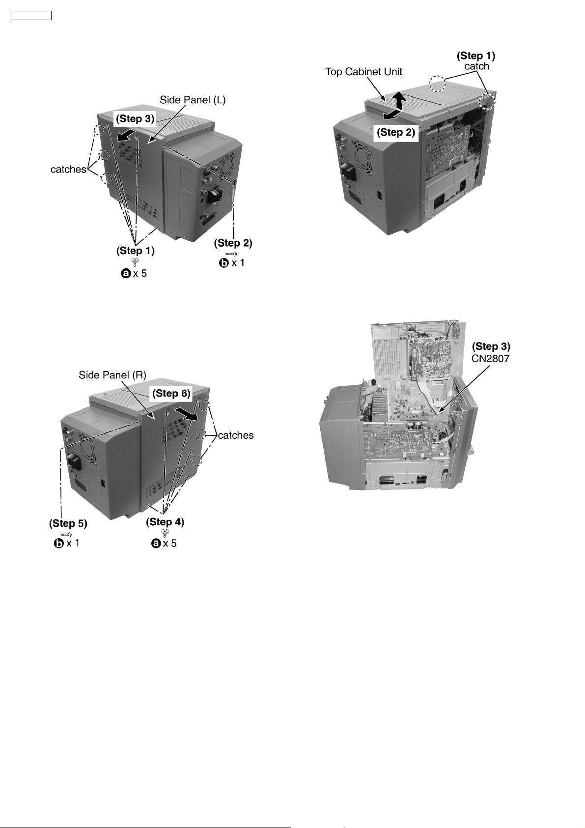
12.2. Disassembly of Side Panel (L)
& (R)
Step 1 : Remove 5 screws.
Step 2 : Remove 1 screw.
Step 3 : Remove the side panel (L) as arrow shown (Be careful
of the catches).
Step 1 : Releas e catches at both ends.
Step 2 : Lift up the top cabinet unit, push backward as arrow
shown and flip top cabinet unit sideway.
Step 4 : Remove 5 screws.
Step 5 : Remove 1 screw.
Step 6 : Remove the side panel (R) as arrow shown (Be careful
of the catches).
12.3. Disassembly of Top Cabinet
Unit
· Follow the (Step 1) - (Step 6) of Item 12.2.
Step 3 : Detach the FFC CN2807.
12.4. Disassembly of Deck
Mechanism and Tape Eject
P.C.B
· Follow the (Step 1) - (Step 6) of Item 12.2.
· Follow the (Step 1) - (Step 3) of Item 12.3.
20
Page 21
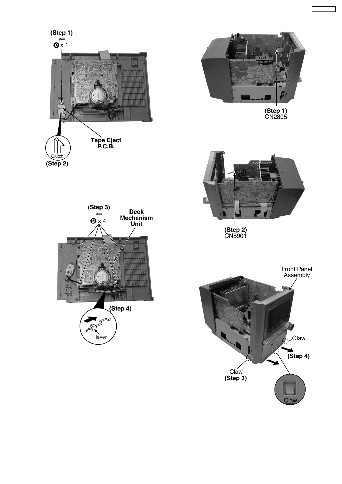
Step 1 : Detach the FFC CN2805.
SA-PM91DEE
Step 1 : Remove 1 screw.
Step 2 : Releas e the clutch.
Step 2 : Detach the connector CN5901.
Step 3 : Remove 4 screws.
Step 4 : Push the lever as arrow shown to open the cassette lid
and remove the deck mechanism unit.
12.5. Disassembly of Front Panel
Assembly
· Follow the (Step 1) - (Step 6) of Item 12.2.
· Follow the (Step 1) - (Step 3) of Item 12.3.
Step 3 : Releas e 3 claws.
Step 4 : Remove the front panel assembly as arrow shown.
12.6. Disassembly of Panel P.C.B
· Follow the (Step 1) - (Step 6) of Item 12.2.
21
Page 22
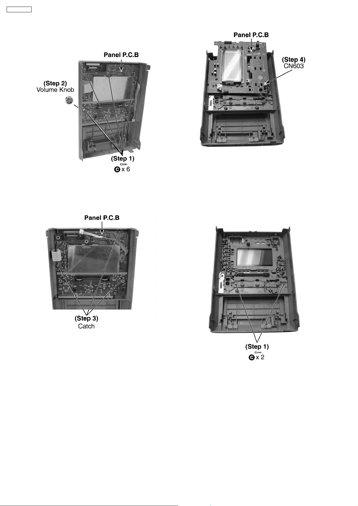
SA-PM91DEE
· Follow the (Step 1) - (Step 4) of Item 12.3.
· Follow the (Step 1) - (Step 4) of Item 12.5.
Step 4 : Detach the connector CN603.
Step 1 : Remove 6 screws.
Step 2 : Remove the volume knob.
Step 3 : Releas e 3 catches.
12.7. Disassembly of Switch P.C.B
· Follow the (Step 1) - (Step 6) of Item 12.2.
· Follow the (Step 1) - (Step 4) of Item 12.3.
· Follow the (Step 1) - (Step 4) of Item 12.5.
· Follow the (Step 1) - (Step 4) of Item 12.6.
Step 1 : Remove 2 screws.
22
Page 23

Step 2 : Releas e 6 catches.
SA-PM91DEE
12.8. Disassembly of Rear Cabinet
· Follow the (Step 1) - (Step 6) of Item 12.2.
· Follow the (Step 1) - (Step 4) of Item 12.3.
Step 3 : Remove the center stage unit as arrow shown.
Step 4 : Release 4 catches to remove the P.C.B support.
Step 1 : Remove 14 screws.
Step 2 : Detach the connector CN2808.
Step 3 : Releas e 2 catches.
Step 4 : Remove the rear cabinet as arrow shown.
12.9. Disassembly of Tuner Pack
· Follow the (Step 1) - (Step 6) of Item 12.2.
· Follow the (Step 1) - (Step 4) of Item 12.3.
· Follow the (Step 1) - (Step 4) of Item 12.8.
Step 5 : Remove the Switch P.C.B as arrow shown.
Step 1 : Detach the connector CN2804 and remove the tuner
pack as arrow shown.
23
Page 24

SA-PM91DEE
12.10. Disassembly of Harmonic
Bass P.C.B
· Follow the (Step 1) - (Step 6) of Item 12.2.
· Follow the (Step 1) - (Step 4) of Item 12.3.
Step 1 : Detach the connec tion CN2817 and remove the
Harmonic Bass P.C.B.
· Follow the (Step 1) - (Step 4) of Item 12.3.
· Follow the (Step 1) - (Step 4) of Item 12.8.
Step 1 : Detach the connection CN5805.
Step 2 : Remove 1 screw.
12.11. Disassembly of Scart Terminal
P.C.B
· Follow the (Step 1) - (Step 6) of Item 12.2.
· Follow the (Step 1) - (Step 4) of Item 12.3.
· Follow the (Step 1) - (Step 4) of Item 12.8.
Step 3 : Remove the Speaker P.C.B as arrow shown.
12.13. Disassembly of Main P.C.B
· Follow the (Step 1) - (Step 6) of Item 12.2.
· Follow the (Step 1) - (Step 4) of Item 12.3.
· Follow the (Step 1) - (Step 4) of Item 12.8.
Step 1 : Lift the Scart Terminal P.C.B slightly outward as arrow
shown.
Step 2 : Detach the connection CN2809 and remove the Scart
Terminal P.C.B.
12.12. Disassembly of Speaker P.C.B
· Follow the (Step 1) - (Step 6) of Item 12.2.
24
Page 25

Step 1 : Detach the FFC CN2806.
Step 2 : Detach the FFC CN2805 and connection CN2801,
CN2802.
SA-PM91DEE
Step 1 : Detach the connector CN5801, CN590 1.
Step 3 : Detach the FFC CN2803.
12.14. Disassembly of Transformer
P.C.B
· Follow the (Step 1) - (Step 6) of Item 12.2.
· Follow the (Step 1) - (Step 4) of Item 12.3.
· Follow the (Step 1) - (Step 4) of Item 12.8.
Step 2 : Remove 4 screws.
12.15. Disassembly of Power P.C.B
· Follow the (Step 1) - (Step 6) of Item 12.2.
· Follow the (Step 1) - (Step 4) of Item 12.3.
· Follow the (Step 1) - (Step 4) of Item 12.8.
· Follow the (Step 1) - (Step 3) of Item 12.13.
Step 1 : Remove 6 screws.
Step 2 : Detach the connector CN5805 & CN5801.
25
Page 26
SA-PM91DEE
Step 3 : Remove the Power P.C.B as arrow shown.
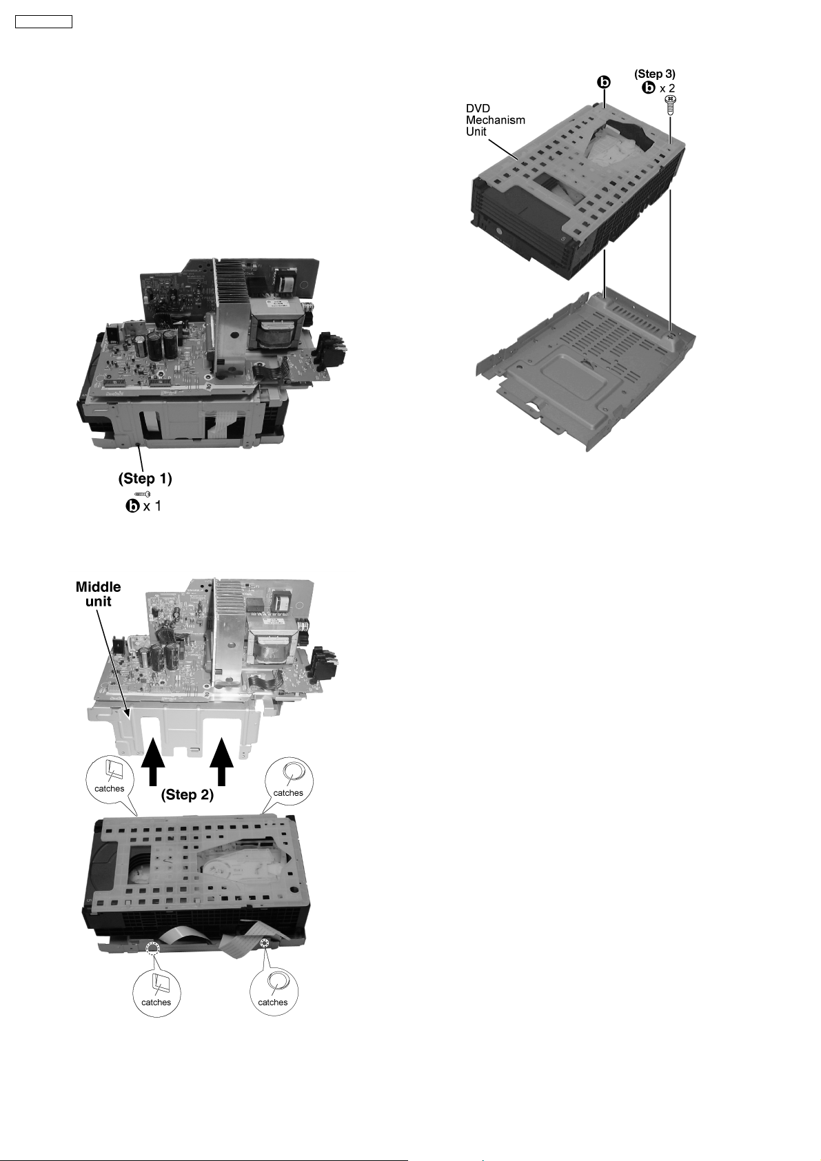
12.16. Disassembly of DVD
Mechanism Unit
· Follow the (Step 1) - (Step 6) of Item 12.2.
· Follow the (Step 1) - (Step 4) of Item 12.3.
· Follow the (Step 1) - (Step 4) of Item 12.5.
· Follow the (Step 1) - (Step 4) of Item 12.8.
· Follow the (Step 1) - (Step 3) of Item 12.13.
Step 1 : Remove 1 screw.
Step 3 : Remove 2 screws and lift up DVD Mechanism unit.
12.17. Checking Procedure for Each
Major P.C.B.
12.17.1. Replacement of the Power
Amplifier IC
· Replacement of the Power Amplifier IC
· Follow the (Step 1) - (Step 6) of Item 12.2.
· Follow the (Step 1) - (Step 4) of Item 12.3.
· Follow the (Step 1) - (Step 4) of Item 12.5.
· Follow the (Step 1) - (Step 4) of Item 12.8.
· Follow the (Step 1) - (Step 3) of Item 12.13.
· Follow the (Step 1) - (Step 2) of Item 12.16.
Step 2 : Release the catches and remove the middle unit as
arrow shown.
26
Page 27
Step 1 : Remove 1 screw and lift up dampe r gear.
Step 2 : Remove the cassette open spring.
SA-PM91DEE
Step 1 Remove 2 screws.
Step 2 Unsold er the terminals of Power Amp IC (IC500) and
replace the component.
12.18. Procedure for Replacing Deck
Holder
· Follow the (Step 1) - (Step 6) of Item 12.2.
· Follow the (Step 1) - (Step 4) of Item 12.3.
· Follow the (Step 1) - (Step 4) of Item 12.4.
Step 3 : Pull out the ribs of the cassette holder to the arrow
direction.
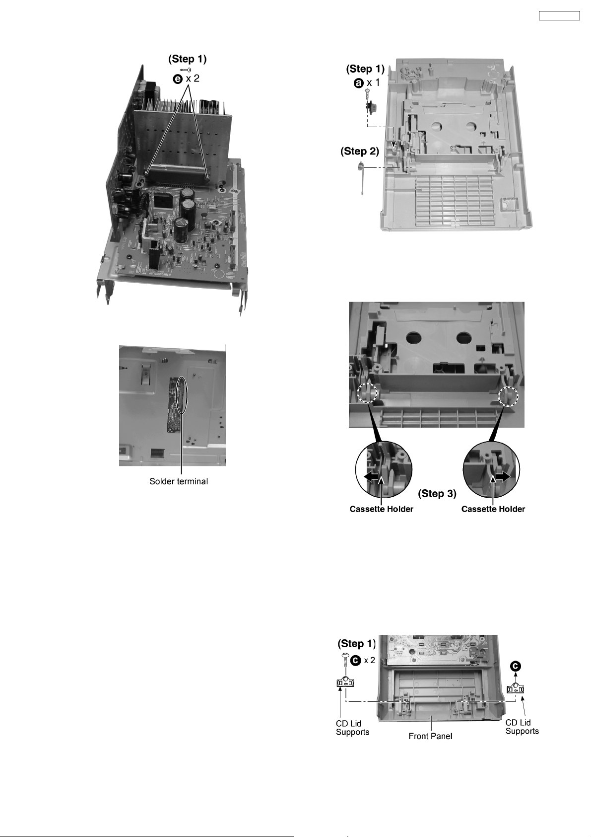
12.19. Replacing for CD Lid
· Follow the (Step 1) - (Step 6) of Item 12.2.
· Follow the (Step 1) - (Step 4) of Item 12.3.
· Follow the (Step 1) - (Step 4) of Item 12.5.
Step 1 : Remove 2 screws and 2 CD lid supports.
27
Page 28
SA-PM91DEE
Step 2 : Push the spring as arrow shown.
Step 3 : Remove the CD lid as arrow shown.
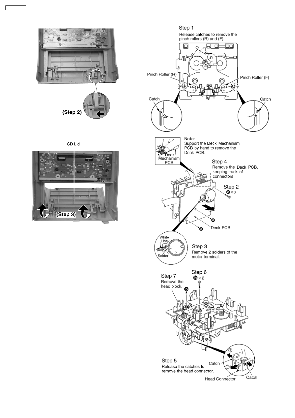
12.20. Procedure for Replacing Pinch
Roller and Head Block (Deck
Mechanism Unit)
· Follow the (Step 1) - (Step 6) of Item 12.2.
· Follow the (Step 1) - (Step 4) of Item 12.3.
· Follow the (Step 1) - (Step 4) of Item 12.4.
28
Page 29

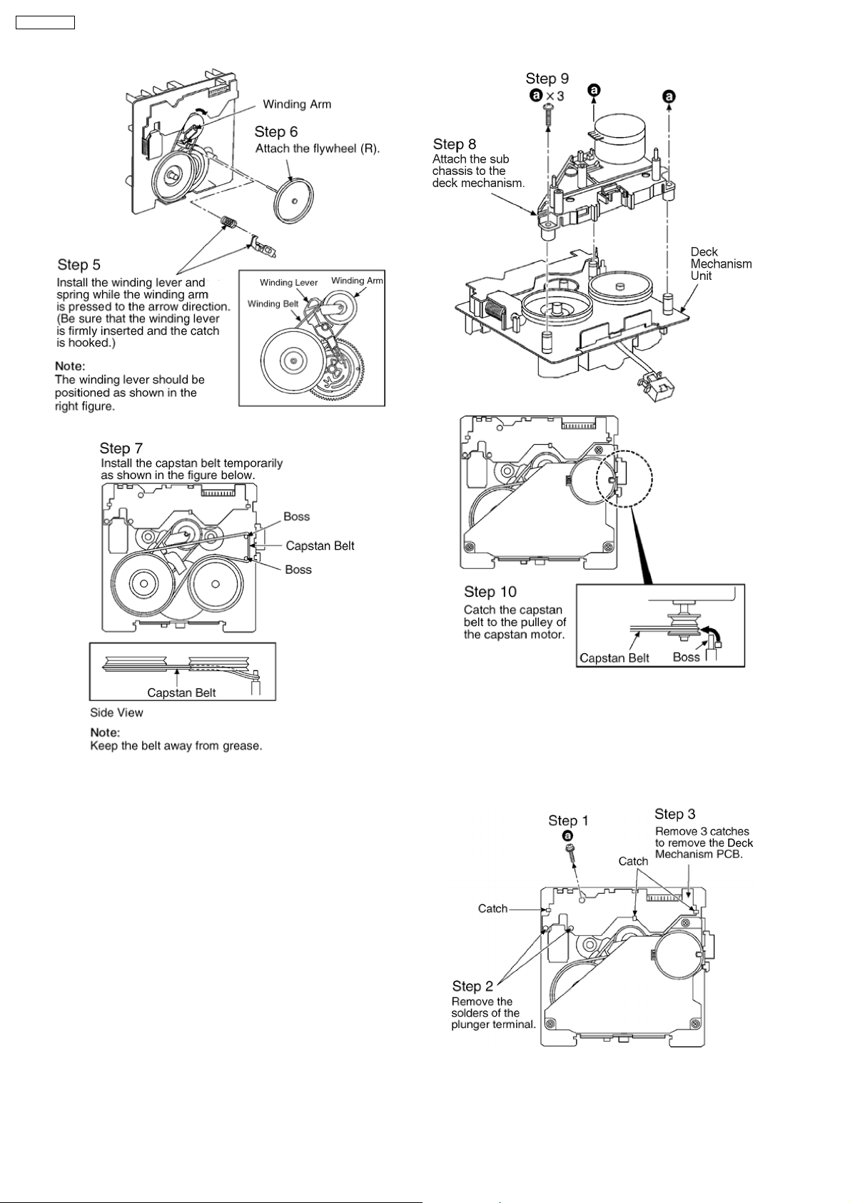
12.21. Procedure for Replacing
Motor, Capstan Belt A,
Capstan Belt B, and Winding
Belt (Deck Mechanism Unit)
· Follow the (Step 1) - (Step 6) of Item 12.2.
· Follow the (Step 1) - (Step 4) of Item 12.3.
· Follow the (Step 1) - (Step 4) of Item 12.4.
· Follow the (Step 1) - (Step 4) of Item 12.20.
SA-PM91DEE
29
Page 30
SA-PM91DEE
12.22. Procedure for Replacing Parts
on Deck Mechanism PCB
· Follow the (Step 1) - (Step 6) of Item 12.2.
· Follow the (Step 1) - (Step 4) of Item 12.3.
· Follow the (Step 1) - (Step 4) of Item 12.4.
12.23. Procedure for removing CR16 mechanism (Precaution)
1. Turn off by pressing power SW in the body.
30
Page 31

2. Unplug AC power cord after the indication of [BYE], then disassemble the body.
3. Disassemble the body, and take out CD loading mechanism.
4. Perform disassembly according to the following procedure for disassembly.
12.24. CR16 mechanism disassembly
procedure
12.24.1. Gear for servicing information
· This unit has a gear which used for chacking items
(open/close of disc tray, up/down operation of traverse unit
by manually) when servicing. (For gear information, that is
described on the items for disassembly procedures.)
· For preparation of gear (for servicing), perform the
procedures as follows.
· In case of re-servicing the same set, the “ gear for servicing”
may be took off becaus e it had been used. So, the “gear for
servicing” must be stored.
1. Remove the gear attached to top cover of CD loading
mechanism.
SA-PM91DEE
2. Insert the hexagonal wrench (2.5mm) into the gear.
12.24.2. Replacement of traverse deck
· Follow the (Step 1) - (Step 6) of Item 12.2.
· Follow the (Step 1) - (Step 4) of Item 12.3.
· Follow the (Step 1) - (Step 4) of Item 12.5.
· Follow the (Step 1) - (Step 4) of Item 12.8.
· Follow the (Step 1) - (Step 3) of Item 12.13.
· Follow the (Step 1) - (Step 4) of Item 12.16.
12.24.3. Replacement of optical pickup unit
· Follow the (Step 1) - (Step 6) of Item 12.2.
· Follow the (Step 1) - (Step 4) of Item 12.3.
· Follow the (Step 1) - (Step 4) of Item 12.5.
· Follow the (Step 1) - (Step 4) of Item 12.8.
· Follow the (Step 1) - (Step 3) of Item 12.13.
· Follow the (Step 1) - (Step 4) of Item 12.16.
· Follow the (Step 1) - (Step 2) of Item 12.24.2.
31
Page 32

SA-PM91DEE
32
Page 33

SA-PM91DEE
33
Page 34

SA-PM91DEE
12.24.4. Disassembly of Traverse Motor
(Unit) and Spindle Motor (Unit)
· Follow the (Step 1) - (Step 6) of Item 12.2.
· Follow the (Step 1) - (Step 4) of Item 12.3.
· Follow the (Step 1) - (Step 4) of Item 12.5.
· Follow the (Step 1) - (Step 4) of Item 12.8.
· Follow the (Step 1) - (Step 3) of Item 12.13.
· Follow the (Step 1) - (Step 4) of Item 12.16.
· Follow the (Step 1) - (Step 2) of Item 12.24.2.
· Follow the (Step 1) - (Step 13) of Item 12.24.3.
34
Page 35

SA-PM91DEE
12.24.5. Replacement for the disc tray
· Follow the (Step 1) - (Step 6) of Item 12.2.
· Follow the (Step 1) - (Step 4) of Item 12.3.
· Follow the (Step 1) - (Step 4) of Item 12.5.
· Follow the (Step 1) - (Step 4) of Item 12.8.
· Follow the (Step 1) - (Step 3) of Item 12.13.
· Follow the (Step 1) - (Step 4) of Item 12.16.
35
Page 36

SA-PM91DEE
36
Page 37

SA-PM91DEE
12.24.6. Replacement for the traverse deck
· Follow the (Step 1) - (Step 6) of Item 12.2.
· Follow the (Step 1) - (Step 4) of Item 12.3.
· Follow the (Step 1) - (Step 4) of Item 12.5.
· Follow the (Step 1) - (Step 4) of Item 12.8.
· Follow the (Step 1) - (Step 3) of Item 12.13.
· Follow the (Step 1) - (Step 4) of Item 12.16.
· Follow the (Step 1) - (Step 10) of Item 12.24.5.
37
Page 38

SA-PM91DEE
12.24.7. Disassembly for loading unit
· Follow the (Step 1) - (Step 6) of Item 12.2.
· Follow the (Step 1) - (Step 4) of Item 12.3.
· Follow the (Step 1) - (Step 4) of Item 12.5.
· Follow the (Step 1) - (Step 4) of Item 12.8.
· Follow the (Step 1) - (Step 3) of Item 12.13.
· Follow the (Step 1) - (Step 4) of Item 12.16.
· Follow the (Step 1) - (Step 10) of Item 12.24.5.
· Follow the (Step 1) - (Step 4) of Item 12.24.6.
38
Page 39

SA-PM91DEE
39
Page 40

SA-PM91DEE
40
Page 41

12.25. CR16 MECHANISM ASSEMBLY
PROCEDURE
The following specified greases and/or oil must be applied
when some specific parts are changed.
1. Floil grease (VFK1298) : The floil grease must be
applied to tray, tray (L) and tray (R).
2. Hanarl oil (VFK1700) : The hanarl oil must be applied to
any parts with grease other than the said parts.
· Follow the (Step 1) - (Step 6) of Item 12.2.
· Follow the (Step 1) - (Step 4) of Item 12.3.
· Follow the (Step 1) - (Step 4) of Item 12.5.
· Follow the (Step 1) - (Step 4) of Item 12.8.
· Follow the (Step 1) - (Step 3) of Item 12.13.
· Follow the (Step 1) - (Step 4) of Item 12.16.
· Follow the (Step 1) - (Step 10) of Item 12.24.5.
· Follow the (Step 1) - (Step 4) of Item 12.24.6.
· Follow the (Step 1) - (Step 22) of Item 12.24.7.
SA-PM91DEE
41
Page 42

SA-PM91DEE
42
Page 43

SA-PM91DEE
43
Page 44

SA-PM91DEE
44
Page 45

SA-PM91DEE
45
Page 46

SA-PM91DEE
46
Page 47

SA-PM91DEE
47
Page 48

SA-PM91DEE
48
Page 49

SA-PM91DEE
49
Page 50

SA-PM91DEE
50
Page 51

SA-PM91DEE
51
Page 52

SA-PM91DEE
52
Page 53

12.26. Disassembly of traverse
mechanism
· Follow the (Step 1) - (Step 6) of Item 12.2.
· Follow the (Step 1) - (Step 4) of Item 12.3.
· Follow the (Step 1) - (Step 4) of Item 12.5.
· Follow the (Step 1) - (Step 4) of Item 12.8.
· Follow the (Step 1) - (Step 3) of Item 12.13.
· Follow the (Step 1) - (Step 4) of Item 12.16.
SA-PM91DEE
53
Page 54

SA-PM91DEE
12.27. Handling of cassette tape jam
· Follow the (Step 1) - (Step 6) of Item 12.2.
54
Page 55

13 Service Positions
13.1. Checking procedure
Note:
For the disassembling procedure, see the section 12.
13.2. Checking the major P.C.B.
SA-PM91DEE
1. Disassembly of Side Panel L & R
2. Disassembly of Top Cabinet
3. Disassembly of Deck Mechanism and Tape Eject P.C.B.
4. Disassembly of Front Panel
5. Disassembly of Panel P.C.B.
6. Disassembly of Switch P.C.B.
7. Disassembly of Rear Cabinet
8. Disassembly of Tuner Pack
9. Disassembly of Harmonic Bass P.C.B.
10. Disass embly of Scart Terminal P.C.B.
11. Disass embly of Speaker P.C.B.
12. Disass embly of Main P.C.B.
13. Disassembly of Transf ormer P.C.B.
14. Disass embly of Power P.C.B.
15. Disass embly of DVD Mechanism
55
Page 56

SA-PM91DEE
14 Self-Diagnosis Function
This unit is equipped with the self-diagnosis function, which display s an error when it occurs, for use during servicing.
14.1. Automatic Displayed Error Codes
14.1.1. Automatic Display Function
For a power unit error, the code is automatically display ed.
F61: Automatically displayed on the LCD of the player.
Fig. 14-1
14.1.2. Re-Display
· For F61 Display
−
− When the code, F61 is displayed, the power is automatically turned off.
− −
−
− The code, F61 is displayed for three seconds, and then the current time appears.
− −
−
− To retrieve the code, turn on the power button so that the code F61 appears, however, is switched to time display after three
− −
seconds, and the power is automatically turned off.
· For F76 Display
−
− The abnormalities of an output or abnormalities in the power supply of POWER AMP IC.
− −
14.1.3. Description of Error Code
14.1.3.1. F61
· State, Condition
When the power is turned on, the unit is automatically turned off. The power does not turn on.
· Cause, Troubleshooting
Power circuit system failure and/or direct current flown to speaker terminal
Identify the cause and replace with new parts.
14.1.4. Setting of Self-Diagnostic (Test Mode)
a) Turn on power for unit.
b) Select DVD/CD Mode. Ensure no disc is inserted in the unit.
c) Press and hold [STOP] and [H.BASS] button for at least 2 seconds. It enters into test mode.
d) Press [POWER] button on the main unit or remote control to exit test mode.
14.2. Memorized Error Codes
14.2.1. Activating Self-Diagnosis Function and Displaying Method
1. Turn on the power.
2. Select DVD/CD function. With no DVD/CD inserted in the player, press and hold down the [STOP] button for at least two
seconds, and press the [0] button on the remote control for at least two seconds in order to display “DVD_xxx ”.
3. Press the [STOP] button. If a memorized error is detecte d, the result of self diagnosis is displayed. (Ex.: H15)
If several errors are detected, press the [STOP] button to display each.
56
Page 57

Fig. 14-2
14.2.2. Re-Display
· Press the power button to turn off the power, and then turn on the power.
· The details of self diagnosis are stored in the unit memory.
To retrieve them, follow the procedure described the above, “Activating Self-Diagnosis Function and Displaying Method”.
14.3. Opecon Version and EEPROM Checksum Display
· Display of Opecon Version and EEPROM checksum if EEPROM exists.
·
1. with EEPROM (verification OK)
SA-PM91DEE
2. No EEPRO M
3. with EEPROM (verification NG)
· During check sum display, if any valid remocon code is received, check sum display cancelled.
14.4. Service Mode Table 1
Following modes are available with combinations of the pressed button s on the player and on the remote controller unit.
Player Remote controller unit Usage
button
0 Error code display
5 Tilt adjustment
6 Region number and broadcasting system check
7 Built-in program version check
DISPLAY DVD laser drive current check
3 CD laser drive current check
PAUSE Writing of laser drive current value after replacement of optical pickup
(Do use this function only when optical pickup is replaced.)
Initialization of the player (factory setting is restored.)
Used after replacement of micro-computer and its peripherals and printed circuit board.
57
Page 58

SA-PM91DEE
14.5. Self-Diagnosis Error Code Description
Code Display Abnormal Item Detection Method
F61 Abnormal output or power supply When DCDET becomes L while operating, PCONT is set to L
H15 OPEN SW It is memorized if there is abnormal SW while operation, and is failH16 CLOSE SW
CD F28 The DISC loading is abnormal Memory when switch is not changed even if it exceeds it to time of
CD F29 The DISC unloading is abnormal
CD F27 DOWN SW is abnormal
CD F22 Mechanism is loading motor/abnormal
without usual POWER OFF processing, and F61 is displayed after
GOOD-BYE display. Occurrence of abnormality shall be
memorized and displayed in the abnormal detection display mode.
save operation, and an abnormal content is displayed by the selfdiagnostic mode usually.
Abnormal SW is detected in the abnormal detection mode.
fail safe time when horizontally operating toward PLAY position
doesn’t enter state of target.
When mechanism begins to operate next time, initialization is done.
Only when backup data is cleared clearly of this error No. when it
compels clearly or power supply start-up.
14.6. DVD/CD Self-Diagnosis Error Code Description
Abnormal display The error is detailed
U11 Focus servo failure
H01 Tray loading failure
H02 Spindle servo failure
H03 Traverse motor failure
H04 Tracking servo error
H05 Seek timeout failure
F010 A specified value is larger than the Parental value of a specified country.
F020 There is no TT_SRPT. (RLBN is 0.)
F021 The number of TT_SRP is 0.
F022 A specified value is larger than the number of TT_SRP.
F023 There is no SRP corresponding to VTSN or VTS_TTN.
F024 A specified value is larger than TT_SRP.P TT_Ns.
F030 The number of TTU_SRP is 0.
F031 A specified value is larger than the number of TTU_SRP.
F040 SRP1 or more is 0.
F041 The number of PGCI_SRP is 0.
F042 A specified value is larger than the number of PGCI_SRP.
F043 There is no PGCI_SRP corresponding to Menu ID.
F050 The number of TMAP_SRP is 0.
F051 A specified value is larger than the number of TMAP_SRP .
F052 Specification TMAP_SA is 0.
F053 The number of MAP_EN is 0.
F060 There is no PGMAP in PGC though C_POSIT exists.
F061 The number of PG in PGC is 0 though C_POSIT exists.
F062 A specified value is larger than the number of PG in PGC.
F063 There is no C_PBIT in PGC though C_POSIT exists.
F064 The number of PG in PGC is 0 though C_POSIT exists.
F065 Specification Cell number is 0.
F066 A specified value is larger than the number of Cell in PGC.
F067 It should be a block cell.
F070 It is not NV_PCK data.
F080 There is no Cell number under the retrieval.
F0E0 The PGC control file for the guide of the user ..DFD.. cannot be eliminated.
F0E1 There is no DFD interchangeable type with DFD main microcomputer. It is not possible to download it.
F0E2 DFD starting download PGC reproduction error
F0E3 DFD download completion waiting PGC reproduction error
F0E4 AVDEC when DFD is downloaded
F0E5 Farm file lead error when DFD is downloaded
F0E6 Falsification check error of firmware that reads DFD
F0F0 There is no farm file and it downloads it DFD unnecessary.
F0F1 There is no firmware corresponding to the DFD download condition and it is unnecessary.
F103 Illegal Highlight Position
F4FF There was no ACK though the compulsion initialization demand was done to Panecon.
F500 DSC Error
F501 DSC Not Ready Error
F502 DSC Time Out Error
F503 DSC Communication Failure
F504 The DSC data slice offset adjustment is abnormal.
F505 DSC Attention Error
58
Page 59

Abnormal display The error is detailed
F506 Media cannot distinguish. (It is invalid media.)
F600 Administrative information cannot be acquired by the recovery error.
F601 Irregular sector ID demand
F602 LEAD-IN information cannot be acquired by the recovery error.
F603 KEY_DET cannot be acquired by the recovery error.
F610 ODC loss of control
F611 CRCOK doesn´t go out during the fixed time. (CD system)
F612 CRCOK doesn´t go out during the fixed time. (DVD system)
F620 Laser protection"State of high temperature"
F621 Laser protection"State of circuit breakdown"
F700 MBX Overflow
F701 Message Command Not Complete Error
F702 Message Command Changed
F880 The task number is inapposite.
F890 It tried to transmit the message while transmitting to the AV task.
F891 The message to the AV task was not able to transmit. (mailbox overflow etc.)
F8A0 The message command is inapposite.
F893 Flash ROM is falsified.
F894 EEPROM, it is not normal.
F895 The language destination is abnormal.
F896 It is a model setting that doesn´t exist.
F897 Cannot it written and the following initialization been done.
F0BB DVD-R cannot reproduce.
F0BC DVD-RAM cannot reproduce.
F0BD CD-R cannot reproduce. Reservation..display.
F0BE CD-RW cannot reproduce. Reservation..display.
F0BF Because a physical layer cannot distinguish, it is not possible to reproduce.
F0C0 It is not DVD Video but it cannot be a reproduction.
F0C1 It prohibits it for the prohibition region code.
F0C2 Reproduction prohibition of PAL
F0C3 All title reproduction prohibition of Parental setting
F0C4 Because it is PHOTO CD format, it prohibits it.
F0C5 Because it is CDROM without VCD/CD:CD-DA, it prohibits it.
F0D0 Length error of retrieved file name
F0D1 Retrieved file or directory was not found.
F630 Non-response to KEY_DET inquiry (It is not CPPM-DISC.)
F631 Even the FILE terminal cannot have done CPPM_KEY_DET.
F632 CPPM_KEY_DET cannot have been done.
9312 ADR is not one.
9F20 OUT of PB AREA
9F30 DATA Track PLAY
9F40 Media type decision (It is data among the drive managers.)
SA-PM91DEE
14.7. Service Mode Table 2
Following modes are available with combinations of the pressed button s on the player and on the remote controller unit.
Item Operational Condition
Error code display While the player is
ADSC internal RAM
display
and Key Function
stopped and no disc is
inserted, press and
hold down the [STOP]
button on the player
and the number
button, “0” on the
remote controller unit.
While the player is
stopped and no disc is
inserted, press and
hold down the [STOP]
button on the player
and the number button
“1” or “2” on the remote
controller unit.
Error code display
Displays the latest error code stored in
EEPROM.
ADSC internal RAM display
Reads and displays the RAM value
inside ADSC. The address is renewed
when the CLEAR key is pressed so
that the values at eleven points appear.
Details Display To Exit Mode
[DVD_---]
*---: Error number
[xxx _DDDD_A]
A :ADSC internal RAM display
mode
xxx : Address
DDDD : RAM value at displayed
address
Values are shown in the
hexadecimal digit. The above
example indicates that ADSC value
at the address, xxx is DDDD.
Automatically exits
the mode after five
seconds.
Press the STOP.
59
Page 60

SA-PM91DEE
Item Operational Condition
and Key Function
Measurement of CD
laser current
electricity
While the player is
stopped and no disc is
inserted, press and
hold down the [STOP]
button on the player
and the number button
“3” on the remote
controller unit.
Display the device
name
While the player is
stopped and no disc is
inserted, press and
hold down the [STOP]
button on the player
and the number button
“4” on the remote
controller unit.
Jitter display While the player is
stopped and no disc is
inserted, press and
hold down the [STOP]
button on the player
and the number
button, “5” on the
remote controller unit.
Region display While the player is
stopped and no disc is
inserted, press and
hold down the [STOP]
button on the player
and the number
button, “6” on the
remote controller unit.
Firm version display While the player is
stopped and no disc is
inserted, press and
hold down the [STOP]
button on the player
and the number
button, “7” on the
remote controller unit.
Region and firm
display
While the player is
stopped and no disc is
inserted, press and
hold down the [STOP]
button on the player
and the number
button, “8” on the
remote controller unit.
User initialization While the player is
stopped and no disc is
inserted, press and
hold down the [STOP]
button on the player
and the number button
on the remote
controller unit.
DVD reset While the user
initialization, press and
hold down the [STOP]
button on the player
and the number button
“ENTER” on the
remote controller unit.
Details Display To Exit Mode
Measurement of CD laser current
electricity
Measures CD laser current electricity
and displays the result together with
the initialization value stored in
EEPROM. After measurement, CD
laser is lit till the power is turned off (or
goes off when the primary power is
[xxx_yyy_DC]
DC : CD laser current electricity
measurement mode
xxx : Current electricity initialization
value stored in EEPROM
yyy : Present value of current
electricity
Automatically exits
the mode after five
seconds.
turned off).
Values are shown in the decimal
digit. The above example indicates
the current electricity initialization
value is xxx mA and its present
value is yyy mA when laser is turned
on.
Display the device name [xxxxxxxxxx] Automatically exits
the mode after five
seconds.
Jitter display
[xxx_yyy_zz]
Press the STOP.
Measures and displays jitter.
Measurement is repeated every
second. Read error counter starts at 0
at the mode setting, and increased by
xxx : Jitter measurement value
yyy : Read error counter
zz : Focus driving value
one as data read fails at target block. A
small defect is allowed to correct by
retry. Any possibility is counted as one
increment. Repetitive errors after retry
increase by two levels or more.
Region display [u__w_xy_zzz]
Values are shown to one decimal
place in the decimal digit.Focus
driving value is displayed in the
hexadecimal digit.
Automatically exits
the mode after five
w : Region number
seconds.
u x : N noPAL P PAL
y: N NTSC 6 PAL60
zzz: Paneconjampa information
Firm version display [srrrxxyzzz]
Automatically exits
the mode after five
s : Model type of Panecon
seconds.
rrr : Release number of Panecon
xxx : Generation of Shiscon (26)
y : Model type of Shiscon
zzz : Release number of Shiscon
Region and firm version display [__r__xyzzz]
Automatically exits
the mode after five
r : Region number
seconds.
x : Generation of Shiscon
y : Model type of Shiscon
zzz : Release number of Shiscon
User initialization
The user setting recovers the factory
setting.
DVD reset
The user setting is returned in the state
of the factory shipment. It doesn´t
[_INITIALIZE_] Automatically exits
the mode after five
seconds.
[_DVD_RESET_ _] Automatically exits
the mode after five
seconds.
initialize it at the time of the laser and
the time of the spindle to develop a
model table initial value of the
corresponding number referring to
Paneconjampa.
60
Page 61

SA-PM91DEE
Item Operational Condition
Laser use time While the player is
Reset laser use time While the usage time 1
Spindle use time While the player is
Reset spindle use
time
Communication error
display
Measurement of
laser current
electricity initialization
value
Measurement of
DVD laser current
electricity
and Key Function
stopped and no disc is
inserted, press and
hold down the [STOP]
button on the player
and the
the remote controller
unit.
is displayed, press and
hold down the [STOP]
button on the player
and the
the remote controller
unit.
stopped and no disc is
inserted, press and
hold down the [STOP]
button on the player
and the
the remote controller
unit.
While the usage time 2
is displayed, press and
hold down the [STOP]
button on the player
and the
the remote controller
unit.
While the player is
stopped and no disc is
inserted, press and
hold down the [STOP]
button on the player
and the “MENU” button
on the remote
controller unit.
While the player is
stopped and no disc is
inserted, press and
hold down the [STOP]
button on the player
and the “PAUSE”
button on the remote
controller unit.
While the player is
stopped and no disc is
inserted, press and
hold down the [STOP]
button on the player
and the “DISPLAY”
button on the remote
controller unit.
button on
button on
button on
button on
Details Display To Exit Mode
Laser usage time
Measures each for DVD and CD
respectively.
Laser usage time reset
Resets both for DVD and CD at once.
Spindle motor usage time [_00_30__ERR]
Usage time 2 reset
Spindle motor usage time
Displays frequency of communication
errors between system computer firm
IC and mechanical computer IC during
DVD module.
Measurement of laser current
electricity initialization value
Memorizes each initialization value of
DVD and CD in EEPROM.
Measurement of DVD laser current
electricity
Measures DVD laser current electricity
and displays the result together with
the initialization value stored in
EEPROM. After measurement, DVD
laser is lit till the power is turned off (or
goes off when the primary power is
turned off).
[_1234_5678]
The numbers in the left show usage
time for DVD laser and those in the
right for CD laser. The four-digit
number is shown by the ten hours in
the decimal digit. The number after
0000 is 9999.
[_0000_0000] Automatically exits
The four-digit number is shown by
the ten hours in the decimal digit.
The number after 00_00 is 99_99.
[_00_00__ERR] Automatically exits
[_00_00__ERR] Automatically exits
[xxx_yyy_DO]
DO : Laser current electricity
measurement mode
xxx : DVD current electricity value
yyy : CD current electricity value
Values are shown in the decimal
digit. The above example indicates
that the current electricity
initialization value is xxx mA at DVD
laser and yyy mA at CD laser when
laser is turned on.
[xxx_yyy_DD]
DD: DVD laser current electricity
measurement mode
xxx: Current electricity initialization
value stored in EEPROM
yyy: Present value of current
electricity
Values are shown in the decimal
digit. The above example indicates
that the current electricity
initialization value is xxx mA and its
present value is yyy mA.
Automatically exits
the mode after five
seconds.
the mode after five
seconds.
Automatically exits
the mode after five
seconds.
the mode after five
seconds.
the mode after five
seconds.
Automatically exits
the mode after five
seconds.
Automatically exits
the mode after five
seconds.
14.8. Tray Lock Function
14.8.1. Setting
· Disc Lock Function
1. With the SELEC TOR on DVD/CD and POWER ON, hold down the [STOP] KEY on the main unit, and then press the
[POWER] KEY on the remote control for 3 seconds to enter to Lock mode A.[_ _ _LOCKED_] will be display ed for 3
seconds, and then current disc will begin playing .
2. In Lock mode A, the following key is disabled.
61
Page 62

SA-PM91DEE
[OPEN/CLOSE]
· Operation Lock Function
1. With the SELECTOR on DVD/CD and POWER ON, hold down the [DVD/CD] KEY on the main unit, and then press the
[POWER] KEY on the remote control for 3 seconds to enter Lock mode B.
[_ _ _ LOCKED_] will be displayed for 3 seconds, and the current disc will begin playing.
2. Lock mode B primarily controls the selector and disc operations, and disena bles for the following keys.
Note:
OPEN/CLOSE
button are invalid and the player displays “___LOCKED_” while the lock function mode is entered.
14.9. Things to Do After Repair (Precaution)
Follow the procedure described below after repair.
1. While the power is on, press the
button to close the tray.
2. Press the power button to turn off the power.
3. Unplug the power cable.
Note:
It is prohibited to unplug the power cable while the tray is opened and to close the tray manually.
This would cause the mechanism unit to be jammed.
14.10. Displaying Self-Diagnostic Results
(Cassette Deck Section) (H01, H02, H03, F01, F02)
1. Enter the self-diagnostic mode, following the instructions described in [14.1.4. Entering Self-Diagnostic Mode].
2. Insert a normal-positioned music tape with erase prevention niches on both Sides A and B. Press [TAPE
] button to activate
the TPS operation so that the tape automatically stops at an interval between music selections.
3. Press [STOP
] and [TAPE ] buttons together on the remote controller. (Recording does not start.)
4. Then, insert a Cr02-positioned blank cassette tape with an erase prevention niche of Side A or B set to the left side.
5. Press[
/FF/ ] button on the remote control. The tape will be forwarded and automatically stop after two seconds.
6. Remove the cassette tape, and set the other side.
7. Press [
8. Press [STOP
/ REW/ ] button on the remote control. The tape will be rewound and automatically stops after two seconds.
] button on the unit.
If an error is found, a self-diagnostic key appears on the display.
If several errors are found, the display shows these keys when [STOP
] button is pressed repeatedly. (Ex.:H01 -H02 - F01 -
H01)
14.11. Error detection for DVD/CD block
Error Code Abnormal Items Possible Cause
F15 CD REST SW abnormal CD traverse position intial setting operation failsfe counter (1000 ms)waiting for REST SW to
H15 The CD tray closes CD disc tray detect switch NG. (Check and replace.)
F26 CD servo LSI command signal
abnormal
F28 DISC LOAD abnormal While going to play position, iffailsafe counter is finished and switch to o change or switch
F29 DISC unload abnormal While going to play position, if failsafe counter is finished and switch no change or switch
F27 Slide operation abnormal During vertical operation, if faisafe timer is finished and switch no change or switch target
F17 Down SW abnormal During vertical operation going to the bottom position, if failsafe timer is finished and switch
F22 Loading Mode/ Mecha abnormal During mecha initialization, Loading mode mechanism abnormal, normal operation cannot be
Abnormal item Error Display Method of detection
turn on. Error No. shall be clear by force or during coldstart.
CD function DTMS command, after system setting, if SENSE = ‘L’ cannot be detected.
Memory shall contain F26 code. After Power on, CD function shall continue, error shall occur
“NO DISC”
Error No. shall be clear by force or coldstart.
target condition was not achieve, this error shall be memorized. Next time mechanism
operates, it shall do coldstart.
Error No. shall be clear by force or coldstart.
target condition was not achieve, this error shall be memorized. Next time mechanism
operates, it shall do coldstart.
Error No. shall be clear by force or coldstart.
condition was not achieve, this error shall be memorized. Next time mechanism operates, it
shall do coldstart. ErrorNo. shall be clear by force or coldstart.
no change or switch target condition was not achieve, this error shall be memorized. The Next
time mechanism operates, it shall do mechanism initialization. Error No. shall be clear by
force or coldstart.
achieve. The next time mechanism operates, it shall do mechanism initialization. Error No.
shall be clear by force or coldstart.
62
Page 63

SA-PM91DEE
Error Code Abnormal Items Possible Cause
F75 CD power abnormal under normal operation (self-diagnostic mode inclusive), check if CDRST is H for SELECTOR
at CD. If it is not H after 1 sec, it shall be memorised as an error.
14.12. Error detection code for Cassette Mechanism Block
Error Code Abnormal Items Possible Cause
H01 MODE SW abnormal Normal operation during mecha transition, MODE SW abnormal is memorised. The content
H02 REC INH SW abnormal
H03 HALF SW abnormal
F01 Reel pulse abnormal
F02 TPS abnormal
of abnormality can be confirmed in the abnormal detection mode explained in the later
section.
The content of abnormality can be confirmed in the abnormal detection mode explained in the
later section.
14.13. Changer Reliability Test 1
1. Enter into test mode. (Refer to section 14.1.4)
2. Press [1] button on the remote control. it enters into ageing mode.
· During this series of operation, the number of its operation shall be shown in the alphanumeric display repeatedly.
It shall start from [ _ _ 00001]
· It shall move up one counter when step 1~8 of the above operations end.
It shall display [ _ _ 00000 ] after [ _ _ 99999] has been reached.
· Press POWER key, tray return to PLAY position and then POWER is OFF.
During test mode, if mecha operation encounters abnormality or time over , retry operation shall be done but aging test mode shall
stop.
Ageing process:
Operation
Tray 1 CLOSE
Tray 1 OPEN
Tray 4 CLOSE
Tray 5 CLOSE
Tray 2 CLOSE
Tray 3 CLOSE
OPEN
CLOSE
READ
CLOSE
CHANGE
READ
CHANGE
READ
CHANGE
READ
CHANGE
READ
CHANGE
(Back to tray 1 and repeat)
Note: To exit ageing mode, press [POWER] button. The unit will power down. Do not unplug the power cord until FL display shows
“GOOD-BYE”. This is to avoid tray jam problem.
14.14. Changer Reliability Test 2
1. Enter into test mode. (Refer to section 14.1.4)
2. Press [2] button on the remote control. it enters into ageing mode.
· During this series of operation, the number of its operation shall be shown in the alphanumeric display repeatedly.
It shall start from [ _ _ 00001]
· It shall move up one counter when step 1~8 of the above operations end.
It shall display [ _ _ 00000 ] after [ _ _ 99999] has been reached.
· Press POWER key, tray return to PLAY position and then POWER is OFF.
During test mode, if mecha operation encounters abnormality or time over , retry operation shall be done but aging test mode shall
stop.
63
Page 64

SA-PM91DEE
Ageing process:
Operation
Tray 1 CLOSE
READ
OPEN
CLOSE
CHANGE
Tray 2 CLOSE
READ
OPEN
CLOSE
CHANGE
Tray 3 CLOSE
READ
OPEN
CLOSE
CHANGE
Tray 4 CLOSE
READ
OPEN
CLOSE
CHANGE
Tray 5 CLOSE
READ
OPEN
CLOSE
CHANGE
(Back to tray 1 and repeat)
Note: To exit ageing mode, press [POWER] button. The unit will power down. Do not unplug the power cord until FL display shows
“GOOD-BYE”. This is to avoid tray jam problem.
14.15. Changer Reliability Test 3
1. Enter into test mode. (Refer to section 14.1.4)
2. Press [3] button on the remote control. it enters into ageing mode.
· During this series of operation, the number of its operation shall be shown in the alphanumeric display repeatedly.
It shall start from [ _ _ 00001]
· It shall move up one counter when step 1~8 of the above operations end.
It shall display [ _ _ 00000 ] after [ _ _ 99999] has been reached.
· Press POWER key, tray return to PLAY position and then POWER is OFF.
During test mode, if mecha operation encounters abnormality or time over , retry operation shall be done but aging test mode shall
stop.
Ageing process:
Operation
Tray 1 OPEN
Tray 2 OPEN
Tray 3 OPEN
Tray 4 OPEN
Tray 5 OPEN
CLOSE
READ
CHANGE
CLOSE
READ
CHANGE
CLOSE
READ
CHANGE
CLOSE
READ
CHANGE
CLOSE
READ
CHANGE
DISC CHECK
(Back to tray 1 and repeat)
Note: To exit ageing mode, press [POWER] button. The unit will power down. Do not unplug the power cord until FL display shows
“GOOD-BYE”. This is to avoid tray jam problem.
64
Page 65

Display Example: [1OP000000] ...TRAY OPEN
[1CL000000] ...TRAY CLOSE
[1CH000000] ...TRAY CHANGING
SA-PM91DEE
65
Page 66

SA-PM91DEE
15 Cautions To Be Taken During Servicing
15.1. Recovery after the dvd player is repaired
· W hen Flash ROM or DVD Module P.C.B. is replaced, carry out the recovery processing to optimize the drive. Playback the
recovery disc to process the recovery automatically.
· Recovery disc (Product number=RFKZD03R005)
· Performing recovery
1. Load the recovery disc (Product number: RFKZD03R005) to the player and run it.
2. Recovery is performed automatically . When it is finished, a message appears on the screen.
3. Remove the recovery disc.
4. Turn off the power.
Note:
This unit requires no initialization process carried out after the traditional DVD players were repaired. When the recovery
measures are taken, the customer setting will return to the factory setting as same as the procedure described in item
“Initialization” is carried out. Write down the contents of the setting before recovery processing, and reset the player.
15.2. DVD Player Firmware Version Upgrade Process
Firmware of DVD player may upgrade to conform to improvement of its performance and quality including operational range,
playability of non-standardized discs, etc. The version upgrade disc contains the recovery function, and the recovery disc is not
necessary.
Note:
Version upgrade process cannot be complete if the AC power is cut off due to power failure and other occasions during the
process. If this occurs, replace FLASH ROM and restart version upgrade. Version upgrade disc number is informed when
ordered.
15.3. Firmware Version Upgrade Process by Using Disc and Recovery
Process
· Recovery process
· Firmware version upgrade process
Both of the above procedures automatically start when the recovery disc is replayed.General CD-R disc allows version upgrade
process and recovery process, making version upgrade through disc simple.
Recovery process: Optimization process of player after replacement of FLASH ROM, EEPROM, or module circuit board
Version upgrade process: Renewal of firmware for improvement of operational range and performance
66
Page 67

15.4. Using Recovery Disc
15.4.1. Recovery Process
1. Insert the recovery disc (RFKZD03R005) to the player to replay.
2. The recovery process automatically starts, and a message of completion prompts on the screen.
3. Remove the disc.
4. Turn off the power.
15.4.2. Version Upgrade Process
1. Insert the recovery disc to the player to replay.
2. The version of player is automatically checked and prompts if necessary.
3. Select version upgrade process using the cursor keys on the remote controller unit. (Select YES or NO)
4. a. If YES is selected, the process starts.
b. If NO is selected, only the recovery process is applied.
5. a. When the version upgrade process is complete, a message of completion appears on the screen. Remove the disc.
b. Follow the instruction appearing on the screen, and remove the disc.
6. Turn off the power.
15.5. Total Usage Time Display
SA-PM91DEE
1. Details of Operation/Display
Keys for Operation:
Laser usage time: While the player is stopped and no disc is inserted, press both the
on the remote controller unit.
Spindle motor usage time: While the player is stopped and no disc is inserted, press both the
button on the remote controller unit.
To reset the usage time, while the usage time is displayed:
Laser usage time: press both the
Spindle motor usage time: press both the
2. Purpose of Use
To obtain reference data of laser and spindle motor systems during failure diagnosis.
To check faulty parts during re-repair.
button on the player and the button on the remote controller unit.
button on the player and the button on the remote controller unit.
button on the player and the button
button on the player and the
67
Page 68

SA-PM91DEE
16 Procedure for Checking Operation of Individual Parts for
Deck Mechanism Unit
16.1. Operation Check with Cassette Tape
1. Pull up the EJECT lever using a rubber band. (Fig. 6)
2. Supply DC5V to MOTOR. (→ MOTOR rotates.) (Fig. 5)
3. Insert a cassette tape to the unit.
4. Supply DC9V to the plunger, and turn the power ON and OFF. (→ Power +PL, -PL) (Fig. 5)
a. FWD PLAY: Supply the plunger power in a flash. (ON: approx. 5msec)
b. FWD FF: Supply the plunger power in a flash at PLAY mode. (ON: approx. 5msec)
c. STOP: Supply the plunger power in a flash at FWD FF mode. (ON: approx. 5msec)
d. REV PLAY: Supply the plunger power in a normal timing at STOP mode. (ON: approx. 200msec)
e. REV REW: Supply the plunger power in a flash at REV PLAY mode. (ON: approx. 50msec)
f. STOP: Supply the plunger power in a flash at FF mode. (ON: approx. 50msec)
Repeat the operation (→ FWD PLAY)
(Note) Other operation may start if a timing of supply ing the plunger power is missed.
16.1.1. Connection Status between Mechanism and Power Supply (Motor, Plunger)
16.1.2. Operative Parts of Mechanism Unit (EJECT lever fitted with rubber band,
Plunger/Rib operation)
16.2. Operation Check without Cassette Tape
1. Pull up the EJECT lever using a rubber band. (Fig. 6)
2. Supply DC5V to MOTOR. (→ MOTOR rotates.)
3. Lift up the mechanism unit’s plunger/rib with the tip of a negative screwdriver, and operate the unit in the same timing as
supplying the power. (Fig. 7)
68
Page 69

SA-PM91DEE
69
Page 70

SA-PM91DEE
17 Measurement And Adjustments
17.1. Cassette Deck Section
17.1.1. Requirements
· Test tape (QZZCFM) (QZZCWAT)
· Normal blank cassette tape (QZZCRA)
· Digital frequency counter
· Oscilloscope
· Electrical voltmeter
· Headphone jack output jig (Fig. 8)
17.1.2. Setting of Unit
· VOLUME: MAX
17.1.3. Preparations
1. Apply under [12. Assembling and Disassembling].
2. Remove 4 screws from the mechanism unit to disassemble. under [12. Assembling and Disassembling].
3. Connect the headphone jack output jig (Fig. 8) to headphone jack.
Fig. 8
Fig. 9
17.1.4. Tape Speed Adjustment
· Normal speed adjustment (only during forward playba ck)
(Product reference value: 3,000±90Hz)
1. Connect a frequency indicator. (Fig. 12)
2. Playback the middle portion of the test tape (QZZCWAT).
3. Adjust the motor screw so that the following output level is produced. (Fig. 10)
Adjustment Range: 3,000 ± 90Hz (a constant speed)
70
Page 71

17.1.5. Bias Voltage Check
1. Connect an electrical voltmeter. (Fig. 12)
2. Set the function to “TAPE” position.
3. Insert a normal blank cassette tape (QZZCRA).
4. While pressing and holding down [
the buttons till the recording pause mode is activated.)
5. Check that the output level is within the standard range.
Standard Range: 14 ± 4mV
REC] button, press [TAPE ] button to pause the recording mode. (Repeat pressing
SA-PM91DEE
Fig. 10
Fig. 11
Fig. 12
17.1.6. Bias Frequency Check
1. Connect a digital frequency counter (Fig. 13).
2. Set the function to “TAPE” position.
3. Insert a normal blank cassette tape (QZZCRA) and press “REC” mode on main unit.
4. Check that the output frequency is within the standard range.
Standard Value: 98 ±8 kHz
Fig. 13
71
Page 72

SA-PM91DEE
18 Voltage Measurement and Waveform Chart
Note:
· Indicated voltage values are the standard values for the unit measured by the DC electronic circuit tester (high-impedance)
with the chassis taken as standard.
Therefore, there may exist some errors in the voltage values, depending on the internal impedance of the DC circuit tester.
· Circuit voltage and waveform described herein shall be regarded as reference information when probing defect point
because it may differ from actual measuring value due to difference of Measuring instrument and its measuring condition
and product itself.
· Measurement with shield ON.
18.1. Voltage Measurement
18.1.1. DVD Module P.C.B.
DVD MODULE P.C.B.
Ref No.
MODE 1234567891011121314151617181920
CD PLAY 3.1 3.0 0 3.0 3.2 3.3 2.9 3.0 0 3.0 3.0 3.3 2.8 3.1 2.8 0 2.8 2.9 3.3 0
STANDBY 00000000000000000000
Ref No.
MODE 21 22 23 24 25 26 27 28 29 30 31 32 33 34 35 36 37 38 39 40
CD PLAY 0 3.3 0 2.3 0 1.3 0 3.3 0 0.5 0 0 0 3.3 0 1.2 0.5 0.3 3.3 3.3
STANDBY 00000000000000000000
Ref No.
MODE 41 42 43 44 45 46 47 48 49 50 51 52 53 54 55 56 57 58 59 60
CD PLAY 2.5 2.9 2.0 1.3 1.8 0.8 0.8 3.3 0 2.5 2.7 2.5 3.3 0 0 2.9 3.3 1.4 0 3.3
STANDBY 00000000000000000000
Ref No.
MODE 61 62 63 64 65 66 67 68 69 70 71 72 73 74 75 76 77 78 79 80
CD PLAY 0 3.3 0 0 0 1.4 0 3.0 2.8 3.2 0 0 1.9 0 1.7 1.9 1.7 0 3.3 0
STANDBY 00000000000000000000
Ref No.
MODE 81 82 83 84 85 86 87 88 89 90 91 92 93 94 95 96 97 98 99 100
CD PLAY 3.3 3.3 3.3 3.3 00001.30000000000.80
STANDBY 00000000000000000000
Ref No.
MODE 101 102 103 104 105 106 107 108 109 110 111 112 113 114 115 116 117 118 119 120
CD PLAY 2.4 2.1 1.8 0.4 0 1.8 0 2.1 2.1 1.8 1.8 1.4 1.4 1.7 1.7 1.7 1.7 3.3 1.9 1.7
STANDBY 00000000000000000000
Ref No.
MODE 121 122 123 124 125 126 127 128 129 130 131 132 133 134 135 136 137 138 139 140
CD PLAY 1.4 0 0.5 0.1 0.2 1.1 2.2 1.7 2.6 2.6 2.6 2.6 2.6 2.6 2.6 2.6 2.6 2.6 1.7 1.7
STANDBY 00000000000000000000
Ref No.
MODE 141 142 143 144 145 146 147 148 149 150 151 152 153 154 155 156 157 158 159 160
CD PLAY 3.3 1.2 1.9 2.2 0 1.7 1.7 1.7 0.4 3.3 0.5 0.4 1.0 1.0 2.2 0.4 0000
STANDBY 00000000000000000000
Ref No.
MODE 161 162 163 164 165 166 167 168 169 170 171 172 173 174 175 176 177 178 179 180
CD PLAY 0 0 1.6 0 1.5 0 3.3 0.1 1.7 1.7 0.9 1.3 0 0 0 0.9 0 3.3 0 3.3
STANDBY 00000000000000000000
Ref No.
MODE 181 182 183 184 185 186 187 188 189 190 191 192 193 194 195 196 197 198 199 200
CD PLAY 0000000003.300.81.60.71.63.30.91.61.41.4
STANDBY 00000000000000000000
Ref No.
MODE 201 202 203 204 205 206 207 208 209 210 211 212 213 214 215 216 217 218 219 220
CD PLAY 0 3.3 1.0 1.6 0 1.6 1.7 1.9 3.3 0.9 2.2 0.8 0 2.6 2.6 3.3 2.0 0 1.3 1.6
STANDBY 00000000000000000000
Ref No.
MODE 221 222 223 224 225 226 227 228 229 230 231 232 233 234 235 236 237 238 239 240
CD PLAY 0.2 0 1.6 0.2 3.3 1.6 00000.201.60.23.31.701.600
STANDBY 00000000000000000000
Ref No.
MODE 241 242 243 244 245 246 247 248 249 250 251 252 253 254 255 256 257 258 259 260
CD PLAY 3.3 1.6 0 0 2.1 0 1.3 0 0 3.4 3.1 1.6 0 3.2 3.2 3.3 0 3.3 2.6 0
STANDBY 00000000000000000000
Ref No.
MODE 261 262 263 264 265 266
CD PLAY 2.6 2.8 0 2.8 3.3 2.9
STANDBY 000000
IC8001
IC8001
IC8001
IC8001
IC8001
IC8001
IC8001
IC8001
IC8001
IC8001
IC8001
IC8001
IC8001
IC8001
72
Page 73

SA-PM91DEE
Ref No.
MODE 1234567891011121314151617181920
CD PLAY 0 2.8 3.3 3.1 3.0 0 3.0 3.2 3.4 3.0 3.0 0 2.8 3.3 2.6 3.3 3.2 3.2 3.1 2.1
STANDBY 00000000000000000000
Ref No.
MODE 21 22 23 24 25 26 27 28 29 30 31 32 33 34 35 36 37 38 39 40
CD PLAY 1.6 0.1 0.1 0.2 0.2 2.0 3.3 0 1.6 1.6 1.7 1.6 0000002.60
STANDBY 00000000000000000000
Ref No.
MODE 41 42 43 44 45 46 47 48 49 50 51 52 53 54
CD PLAY 0 2.8 0 3.1 3.1 0 0 3.0 3.3 2.8 2.8 0 0 0
STANDBY 00000000000000
Ref No.
MODE 12345678
CD PLAY 3.3 0 0 2.0 4.6 0 0 4.9
STANDBY 00000000
Ref No.
MODE 1234567891011121314151617181920
CD PLAY 1.7 1.7 1.7 1.8 1.8 1.7 0 4.9 3.3 0 2.4 2.5 2.5 4.4 4.4 4.4 4.9 3.8 0 3.3
STANDBY 00000000000000000000
Ref No.
MODE 21 22 23 24 25 26 27 28
CD PLAY 9.2 9.1 1.7 1.7 1.7 1.7 3.3 3.1
STANDBY 00000000
Ref No.
MODE 12345678910111213141516
CD PLAY 0 3.3 2.9 3.3 1.7 0.8 1.7 1.7 0 0 5.50 0 2.5 2.4 2.4 4.9
STANDBY 0000000000000000
Ref No.
MODE 1 2 3
CD PLAY 0 3.1 3.3
STANDBY 0 0 0
Ref No.
MODE 12345
CD PLAY 0.6 1.3 0 0 1.2
STANDBY 00000
Ref No.
MODE 12345678
CD PLAY 00003.3003.3
STANDBY 00000000
Ref No.
MODE 1234567891011121314151617181920
CD PLAY 0.9 0.8 2.9 0.8 0.8 0.8 2.6 0.8 3.4 0 3.3 3.1 3.3 3.3 0.7 2.1 2.4 1.2 2.4 2.4
STANDBY 000000000000000.400000
Ref No.
MODE 21 22 23 24 25 26 27 28 29 30 31 32 33 34 35 36 37 38 39 40
CD PLAY 2.1 0 2.6 2.6 2.7 2.4 0 2.3 0.7 0.8 0.8 0.7 1.5 0 1.6 1.5 0 1.4 0.9 1.7
STANDBY 00000000000000000000
Ref No.
MODE 41 42 43 44 45 46 47 48
CD PLAY 1.7 1.6 2.0 1.8 2.2 0 3.3 0.5
STANDBY 00000000
Ref No.
MODE 12345
CD PLAY 3.0 3.0 0 0 4.9
STANDBY 00000
Ref No.
MODE 12345
CD PLAY 2.8 2.8 0 0 4.9
STANDBY 00000
Ref No.
MODE E C B E C B E C B E C B E C B
CD PLAY 0 0 1.3 0 4.5 0 0 4.2 0 5.0 4.9 4.2 0 4.9 0.1
STANDBY 0 0 0 0 0 0 0 0 0 0 0 0 0 0 0
Ref No.
MODE E C B E C B 1 2 3 E C B E C B
CD PLAY 4.9 0 4.9 0 0 0.7 0.5 3.7 1.1 4.3 2.3 3.7 3.4 3.3 0.1
STANDBY 0 0 0 0 0 0 0 0 0 0 0 0 0 -1.0 0
Ref No.
MODE E C B E C B
CD PLAY 0 0 0.6 0 3.1 0
STANDBY 0 0 0 0 0 0
QR8111 QR8112
Q8552 Q8560 Q8561 Q8562 QR8571
Q8606 Q8607
IC8051
IC8051
IC8051
IC8111
IC8251
IC8251
IC8420
IC8601
IC8606
IC8611
IC8651
IC8651
IC8651
IC8691
IC8695
QR8420 Q8550 Q8551
18.1.2. CD Loading P.C.B.
Ref No.
MODE 123456789
CD PLAY 7.5 0 0 0 7.5 7.5 4.8 0 4.8
STANDBY 1.7 0 0 0 1.7 1.7 2.7 0 2.8
Ref No.
MODE 123456789
CD PLAY 7.5 0 0 0 7.5 7.5 4.8 0 4.8
STANDBY 1.7 0 0 0 1.7 1.7 2.7 0 2.7
Ref No.
MODE 1234
CD PLAY 0.3 1.2 0 0
STANDBY 0000
Q1
CD LOADING P.C.B.
IC 11
IC 21
73
Page 74

SA-PM91DEE
18.1.3. Main P.C.B.
MAIN P.C.B.
Ref No.
MODE 1234567891011121314151617181920
CD PLAY 0 5.1 5.1 5.1 0.3 00000.60.75.02.50-5.15.14.93.65.1
STANDBY 0 5.0 5.0 0000000.70.75.12.502.45.25.15.13.55.0
Ref No.
MODE 21 22 23 24 25 26 27 28 29 30 31 32 33 34 35 36 37 38 39 40
CD PLAY 5.0 5.0 0 0 0 5.1 5.0 5.0 5.0 5.0 1.6 0 0 0 3.9 4.0 4.4 0 0 5.0
STANDBY 000005.03.43.65.15.10.900000.10.1000
Ref No.
MODE 41 42 43 44 45 46 47 48 49 50 51 52 53 54 55 56 57 58 59 60
CD PLAY 0 5.0 0 0 5.1 0000000002.500000
STANDBY 00005.10000000002.600000
Ref No.
MODE 61 62 63 64 65 66 67 68 69 70 71 72 73 74 75 76 77 78 79 80
CD PLAY 0 5.1 000005.105.003.200001.504.34.9
STANDBY 0 5.1 00000005.10000000000
Ref No.
MODE 81 82 83 84 85 86 87 88 89 90 91 92 93 94 95 96 97 98 99 100
CD PLAY 0 0 0 4.1 2.1 4.8 5.1 3.1 5.0 5.0 2.2 5.0 0.4 2.5 3.8 0 5.0 5.0 5.0 0
STANDBY 00000000002.35.10.42.53.805.05.05.00
Ref No.
MODE 12345678
CD PLAY 0 5.0 000000
STANDBY 0 5.2 000000
Ref No.
MODE 12345
CD PLAY 14.1 2.5 0 1.2 3.0
STANDBY 0.5 0000
Ref No.
MODE 12345
CD PLAY 14.1 6.0 0 1.2 4.9
STANDBY 0.5 0000
Ref No.
MODE 12345
CD PLAY 2.5 5.0 1.4 1.0 0
STANDBY 00000
Ref No.
MODE 12345
CD PLAY 5.9 5.9 5.0 0 0
STANDBY 00000
Ref No.
MODE 12345
CD PLAY 5.9 5.9 5.0 0 0
STANDBY 00000
IC2801
IC2801
IC2801
IC2801
IC2801
IC2802
IC2803
IC2804
IC2805
IC2806
IC2807
74
Page 75

SA-PM91DEE
Ref No.
MODE 1234567891011121314151617181920
CD PLAY 4.9 2.3 4.9 0 0 1.7 2.4 000004.92.34.92.302.22.20
STANDBY 00000000000000.14.90.20000
Ref No.
MODE 21 22 23 24 25 26 27 28 29 30 31 32 33 34
CD PLAY 2.2 2.3 0 2.2 2.2 0 1.8 1.8 0 1.7 1.7 0 2.2 4.9
STANDBY 00000000000000
Ref No.
MODE 123456
CD PLAY 0 2.5 5.0 2.5 0 2.5
STANDBY 00000-0.1
Ref No.
MODE 123456
CD PLAY 0 2.5 5.0 2.5 0 2.5
STANDBY 0 0 0 0.4 0 0.4
Ref No.
MODE 12345678910111213141516
CD PLAY 2.5 2.5 4.9 0 2.5 2.4 0 2.6 2.5 0 5.0 0 0 - 2.5 0
STANDBY 0.2 00000.20000000000
Ref No.
MODE 1234567891011121314151617181920
CD PLAY 4.3 4.3 4.3 4.3 0 4.3 4.3 4.3 4.3 4.3 4.3 4.3 4.3 4.3 4.3 4.3 4.3 0 0 0
STANDBY 0.3 0.3 0.3 0.3 0 0.4 0.4 0.4 0.4 0.3 0.3 0.3 0.3 0.3 0.3 0.3 0000
Ref No.
MODE 21 22 23 24 25 26 27 28 29 30 31 32 33 34 35 36 37 38 39 40
CD PLAY 8.6 0 4.3 4.3 4.3 4.3 4.3 4.3 4.3 4.3 4.3 4.3 4.3 4.3 4.3 4.3 4.3 4.3 4.3 4.3
STANDBY 0 0 0.1 0.1 0.1 0.1 0.1 0.1 0.2 0.2 0.1 0.1 0.1 0000000
Ref No.
MODE 12345678
CD PLAY 0 0 0 -9.1 0 0 0 9.0
STANDBY 00000000
Ref No.
MODE 12345678
CD PLAY 0 0 0 -9.1 0 0 0 9.0
STANDBY 00000000
Ref No.
MODE E C B E C B E C B E C B E C B
CD PLAY 0 0 0 0 0 -6.3 0 0 -6.3 0 0 0 0 0 -6.3
STANDBY 0 0 0 0 0 0 0 0 0 0 0 0 0 0 0
Ref No.
MODE E C B E C B 1 2 3 E C B E C B
CD PLAY 0 0 -6.3 0 0 -6.3 0 0 -6.3 0 5.0 0 0 4.2 0
STANDBY 0 0 0 0 0 0 0 0 0 0 5.0 0 0 0 0
Ref No.
MODE E C B E C B E C B E C B E C B
CD PLAY 10.0 0 10.0 0 0 0.2 0 3.1 0 0 10.0 0 0 -1.3 0
STANDBY 0.2 0 0.2 0 0 0 0 0 0 0 0.2 0 0 -3.2 0
Ref No.
MODE E C B E C B E C B E C B E C B
CD PLAY 0 -1.3 0 0 -6.2 0 0 0 3.7 5.0 5.0 4.3 5.0 4.9 4.3
STANDBY 0 -3.2 0 0 0 0 0 5.2 0 5.2 5.2 4.5 5.2 0 5.2
Ref No.
MODE E C B E C B E C B E C B E C B
CD PLAY 0 0 0 0 10.0 0 0 10.0 0 0 0 4.2 5.8 7.6 5.1
STANDBY 0 0 0 0 0.2 0 0 0.2 0 0 0 0 1.7 1.7 1.2
Q2101
Q2203
Q2806
Q2811 Q2812 Q2813 Q2814 Q2815
Q2102 Q2201Q2103
Q2204 Q2803 Q2805
Q2807
IC2808
IC2808
IC2809
IC2810
IC2811
IC2812
IC2812
IC2813
IC2814
Q2205
Q2808 Q2809
Q2826 Q2827Q2816 Q2817 Q2818
Q2202
Q2810
18.1.4. Harmonic Bass P.C.B.
Ref No.
HARMONIC BASS P.C.B.
MODE 12345678
CD PLAY 0 0 0 -9.2 0 0 0 9.1
STANDBY 0 0 0 -0.2 0000
Ref No.
MODE 12345678
CD PLAY 0 0 0 -9.2 0 0 0 9.1
STANDBY 0 0 0 -0.2 0000
Ref No.
MODE 12345678
CD PLAY 0 0 0 -9.2 0 0 0 9.1
STANDBY 0 0 0 -0.2 0000
Ref No.
MODE E C B E C B E C B E C B
CD PLAY 0 0 -0.9 0 0 -0.9 0 -0.7 0 0 -0.7 0
STANDBY 0 0 -2.1 0 0 -2.1 0 -2.1 0 0 -2.1 0
IC2816
IC2817
IC2818
Q3002 Q3003Q3000 Q3001
75
Page 76

SA-PM91DEE
18.1.5. Panel P.C.B.
PANEL P.C.B.
Ref No.
MODE 1234567891011121314151617181920
CD PLAY -29.5 -29.4 -29.4 -29.5 5.0 3.0 4.1 2.1 0 0 5.1 2.2 2.2 0 -27.5 -31.4 -23.4 -25.4 -23.4 -31.6
STANDBY 00000000000000000000
Ref No.
MODE 21 22 23 24 25 26 27 28 29 30 31 32 33 34 35 36 37 38 39 40
CD PLAY -25.4 -29.5 -27.5 -31.7 -25.5 -23.3 -23.4 -29.6 -25.4 -29.5 -21.3 -25.4 -25.4 -27.5 -23.4 -23.4 -25.3 -25.4
STANDBY 00000000000000000000
Ref No.
MODE 41 42 43 44 45 46 47 48 49 50 51 52 53 54 55 56 57 58 59 60
CD PLAY -25.4 -31.6 -21.3 -25.4 -25.4 -25.4 -31.7 -29.6 -29.5 -29.5 -29.5 -29.5 -29.5 -29.5 -29.5 -29.5 -29.5 -29.5 -29.5 -29.5
STANDBY 00000000000000000000
Ref No.
MODE 61 62 63 64
CD PLAY -29.5 -29.5 -29.5 -29.5
STANDBY 0000
Ref No.
MODE E C B E C B E C B E C B E C B
CD PLAY -33.0 5.0 -33.1 -33.0 5.0 -33.1 0 0 0.8 0 3.1 -0.4 0 3.6 0
STANDBY 0 0 0 0 0 0 0 0 0 0 0 0 0 3.8 0
Q601 Q602 Q603 Q611 Q680
IC601
IC601
-29.5 -27.5
IC601
IC601
18.1.6. Deck P.C.B.
Ref No.
DECK P.C.B.
MODE 12345
CD PLAY 6.1 0000
STANDBY 00000
Ref No.
MODE 1234567891011121314151617181920
CD PLAY 0 0.7 5.2 4.4 0 4.9 0 0 0 6.0 0 8.9 00003.80.24.45.1
STANDBY 0 0.3 0.3 0.3 000000000000000.30.3
Ref No.
MODE 21 22
CD PLAY 0.7 0
STANDBY 0.3 0
Ref No.
MODE E C B E C B E C B E C B E C B
CD PLAY 0 0 0.7 0 0 0.7 2.0 1.9 0 0 5.8 0 5.8 0 5.8
STANDBY 0 0 0 0 0 0 0 0 0 0 0 0 0 0 0
Ref No.
MODE E C B E C B E C B E C B E C B
CD PLAY 0 0 0.6 0 4.9 0 0 8.8 0 0 8.8 0 0 0 0
STANDBY 0 0 0 0 0 0 0 0 0 0 0 0 0 0 0
Ref No.
MODE E C B E C B E C B E C B
CD PLAY 10.0 -0.1 10.0 10.0 0 10.0 0 9.4 -0.2 0 0 0
STANDBY 0.2 -0.2 0.2 0.2 0 0.2 0 0 -0.2 0 0 0
Q1101 Q1201 Q1302 Q1303
Q1306 Q1307 Q1309 Q1310 Q1312
Q1314 Q1315 Q1316 Q1317
IC 1000
IC 1001
IC 1001
Q1304
18.1.7. Deck Mechanism P.C.B.
Ref No.
MODE 1234
CD PLAY 2.5 4.9 3.8 4.9
STANDBY 0000
DECK MECHANISM P.C.B.
IC971
18.1.8. Scart Terminal P.C.B.
Ref No.
MODE E C B E C B E C B E C B E C B
CD PLAY 6.3 6.3 0 0 0 5.0 0 5.0 0.1 6.9 12.5 6.4 0 0 4.2
STANDBY 0.5 0 0.5 0 0.4 0 0 0 0.6 0.7 0.7 0.6 0 0.5 0
Q2819 Q2820 Q2821 Q2822 Q2823
SCART TERMINAL P.C.B.
76
Page 77

18.1.9. Power P.C.B.
SA-PM91DEE
POWER P.C.B.
Ref No.
MODE 123456789101112131415161718
CD PLAY -34.5 34.2 0 34.2 -34.5 0 0 0.7 0 -15.1 00000034.2 -34.5
STANDBY -0.4 0.4 0 0.4 -0.4 0000-0.4 0000000.4-0.4
Ref No.
MODE E C B E C B E C B E C B E C B
CD PLAY -0.8 9.2 -0.1 -0.9 9.2 -0.2 -0.8 9.2 -0.1 -0.9 9.2 -0.2 9.2 32.9 9.8
STANDBY 0 0 0 0 0 0 0 0 0 0 0 0 0 0.3 0.3
Ref No.
MODE E C B E C B E C B E C B E C B
CD PLAY -9.3 -33.1 -9.8 9.3 15.7 9.9 16.3 10.1 15.7 16.5 15.6 16.4 12.4 33.8 13.0
STANDBY -0.1 -0.5 -0.5 0 0.1 0.5 0.5 0.2 0.4 0.5 0.4 0.5 0.5 0.4 0.4
Ref No.
MODE E C B E C B E C B E C B
CD PLAY 0 -9.8 -0.6 0 3.1 0 0 3.1 0 0 4.2 -0.2
STANDBY 0 -0.4 0 0 0 0 0 0 0 0 0 0.1
Q5101 Q5102 Q5201 Q5202
Q5802 Q5803 Q5804
IC500
Q5805
Q5801
Q5806
18.1.10. Transformer P.C.B.
Ref No.
TRANSFORMER P.C.B.
MODE E C B E C B E C B E C B
CD PLAY -32.4 -58.6 -33.0 0 0 0.6 0 3.6 -0.2 6.0 11.8 6.6
STANDBY 0.2 -0.1 0 0 6.0 0 0 3.6 -0.2 6.0 9.0 6.6
Q5904Q5901 Q5902 Q5903
Q5807 Q5808 Q5809 Q5810
77
Page 78

SA-PM91DEE
18.2. Waveform
CN2801 PIN 1
CD PLAY
1.18Vp-p (10msec.div)
CN2803 PIN 3
CD PLAY
5.24Vp-p (10msec.div)
CN2805 PIN 12
CD PLAY
5.44Vp-p (10msec.div)
CN2801 PIN 8
CD PLAY
5.28Vp-p (10msec.div)
CN2803 PIN 21
CD PLAY
4.24Vp-p (500nsec.div)
CN5901 PIN 2
CD PLAY
5.52Vp-p (10msec.div)
CN2803 PIN 1
CD PLAY
5.24Vp-p (10msec.div)
CN2805 PIN 10
CD PLAY
5.28Vp-p (10msec.div)
CN5901 PIN 3
CD PLAY
5.56Vp-p (10msec.div)
CN2803 PIN 2
CD PLAY
4.20Vp-p (10msec.div)
CN2805 PIN 11
CD PLAY
5.36Vp-p (10msec.div)
H5902 PIN 1
CD PLAY
72.4Vp-p (10msec.div)
H5902 PIN 2
CD PLAY
72.8Vp-p (10msec.div)
H5902 PIN 5
CD PLAY
72.8Vp-p (10msec.div)
H5902 PIN 8
CD PLAY
1.24Vp-p (10msec.div)
78
Page 79

19 Block Diagram
19.1. DVD Module Block
SA-PM91DEE
OPTICAL PICKUP
B
QR8571
HFM
VCC
HFM
SUPPLY
SWITCH
CONTROL
Q8552
Q8551
OUT
LDDVD
SWITCH
SWITCH
Q8562
Q8561
LDCD
SWITCH
SWITCH
LDU
17
LD(DVD)
16
LD(CD)
15
SW
8
SUBSEL
1M
PIN(CD)
PIN(DVD)
VREF
SUB2
SUB1
13
11RF9
14
SUB1
SUB2
VREF1
RF
VREF2 (RF-)
FE2
FE1
7
6
FE1(DVD/CD)
FE2(DVD/CD)
TC
4
TC(DVD)
5
TD(DVD)
TD
TB
TA
2
TB(DVD)
3
TA(DVD)
13
TRACKING COIL
T-
T+
14
11
V01-
V01+
VIN3
MUTE12
23
9
FOCUS COIL
F-
F+
12
V02-
MUTE4
20
V02+
IC8251
C0GBG0000048
MOTOR DRIVE
MUTE3
27
TRVM+
15
V04+
VIN1
28
2
16
LDCNT
SPM+
TRVM-
17
V04-
VIN2
3
SPINDLE MOTOR UNIT
SPM-
5
6
18
V03-
V03+
OPIN-
OPOUT
1
BIAS1
4
OPIN+
24
LDIN
25
BIAS2
26
TRIN
TRV_INNER_SW
R
143
124
78
DRV3
LPC01
126
AD0
LPC02
134
125
130
133
110
123
LPC2
LPC1
129
127
VIN9
VIN5
VIN6
VIN10
VREFH
82
DRV7
111
RFINN
132
RFINP
136
115
137
135
131
VIN8
VIN3
VIN7
VIN3RF
138
114
116
VIN2
VIN4
VIN2RF
VIN4RF
MN2DS0003APH
OSCO
OSCI
166
165
X8621
117
VIN1
IC8001
VIN1RF
DV2.1
76
83
DRV1
146
79
DRV8
DRV4
147
VCOF/AD4
PWM1
148
139
AD2
PWM0
75
DRV0
81
128
140
AD1
DRV6
VHALF
79
Page 80

SA-PM91DEE
D8550
Q8560
Q8550
SWITCH
SWITCH
B
IC8601
C0EBE0000384
RESET IC
DQ0
2,4,5,7,8,10,11,
13,42,44,45,47,
48,50,51,53
1,2,4,5,7,8,10,
11,13-15,17,18,
252,254,256
MDQ0
DQ15
MDQ15
A0
22-26,
29-35
217,220,221,223
224,226-228,230,
233,237,238
MA0
IC8051
C3ABPG000133
64 SDRAM
A11
20
234
MA11
IC8651
RFKWMH82H160
16M FLASH ROM
/WE
/RAS
/CS
UDQM
BA1
LDQM
BA0
39
21
15
38
19
232
BA0
243
249
251
240
BA1
DQM1
DQM0
NCSM
/CAS
CLK
MCK
16
17
18
244
245
248
241
NWE
MCKI
NCAS
NRAS
A16
9,10,16,17,48
21,30,31,43,45
EXADR16
A20
EXADR20
MN2DS0003APH
A0
1-8,18-25
23-25,27,32,
33,36,37,39-42,
46,47,50,51
EXADT0
IC8001
A15
EXADT15
DV2.1
DQ0
39-36, 38-45
192-195,197-200,
203,204,206-208
210-212
MDQ16
DQ15
11
22
MDQ31
XWE
NEXWE
26
38
XRESET
XCE
28
52
NEXCE
XOE
NEXOE
12
R
Q8607
SWITCH
Q8606
SWITCH
IC8606
C0EBA0000031
RESET IC
IC8611
C3EBGC000044
16M EEPROM IC
(NOT SUPPLIED)
VCC
B
SDA
SCL
5
6
73
59
60
P9
NRST
P8
80
Page 81

MIXL(R)
FL(R)
ZFLAG&AMUTE
CMD
IECOUT
SA-PM91DEE
A
QR8111
QR8112
SWITCH
SWITCH
B
DSPCLK
TO MAIN
BLOCK
STATUS
P2
5
IC8111
C0CBCBD00018
3.3V
REGULATOR
8
5
5
4
IC8691
C0JBAA000346
LOGIC IC
1
2
68
P3
10(9)
15(14)
VOUT3(4)
VOUTL(R)
IC8420
C0FBBK000049
AUDIO DAC
ZERO2
MS
MC
MD
LRCK
SCK5BCK7DATA16LRCK
163
170
ADOUT3
SRCK
57
DACCK
171
8
169
16
34
2
QR8420
MUTING
SWITCH
56
53
55
P11
P13
P12
P15
149
PY/Y/G
151
DAC1OUT
PB/CB/B
152
DAC2OUT
PR/CR/R
156
DAC3OUT
Y
158
DAC4OUT
C
DAC5OUT
B
TO MAIN
BLOCK
70
177
P1
IECOUT
4
IC8695
C0JBAA000346
LOGIC IC
2
1
69
MN2DS0003APH
IC8001
DV2.1
81
Page 82

SA-PM91DEE
19.2. Main Block
(DECK 2)
R/P HEAD
(DECK 2)
ERASE HEAD
LCH
LCH
IC1001
AN7326K
P/B REC AMP
22(1)
PB LIN(R)
IC1000
C1AA00000612
ANALOG SWITCH
2
4
FILTER
B
20(3)
PB L EQ(R)
Q1317
BEAT PROOF
LEVEL SWITCH
19(4)
MUTE
PB LOUT(R)
18
ALC LOW OUT
TPS
TPS OUT
6
21(2)
PB L NF(R)
3
5
17
TPS
GAIN ADJ
16(7)
REC
L1301
LIN(R)
15(8)
REC
L OUT(R)
REC AMP (L)
B
ALC
14
ALC
Q1309,
Q1310,
Q1312
BIAS
SWITCH
13
NOR/CRO SW
LOGIC
12
VCC
RIPPLE
REJECTION
SWITCH
9
10
RF
PB/REC SW
Q1101
(Q1201)
Q1302
MUTING
SWITCH
DECK
MUTING
CONT
IC971
CNB13030R2AU
PHOTO
INTERRUPTER
79
PHOTO
JOG_A
76
VR601
VOLUME JOG
D1301
S971
89
DECK_AD1
(MODE)
S972
(HALF)
S974
(RECINH_R)
S975
(RECINH_F)
KEY2
92
S607~S610,
S616~S621
KEY SW
B
S601~S606,
Q1304
Q1303
KEY1
97
S611~S615
KEY SW
SWITCH
(REC:H)
SWITCH
78
REC
80
DMT
Q1306
SWITCH
IC2802
C3EBEG000072
EEPROM
(NOT SUPPLIED)
4
3
25
E_CS
JOG_B
75
5
6
24
23
E_DA
E_CLK
C2CBJG000573
MICROPROCESSOR
IC2801
Q1307
SWITCH
90
DECK_AD2
82
Page 83

JK2805
SCART
TERMINAL
BLUEIN
SA-PM91DEE
7
22
CBOUT
2
CIN
C_OUT
GREENIN
REDIN_CIN
VOUT_YIN
FUNCSW
Q2821
SWITCH
RGB_CTRL
16
11
11
19
8
JK2802
VIDEO OUT
JK2802
S.VIDEO OUT
G Y
Q2819,Q2820,Q2822
D2813
IC2809
C1AB00001731
VIDEO BUFFER IC
IC2810
C1AB00001731
VIDEO BUFFER IC
CG
SWITCH
Q2823
SWITCH
B
Q603
SWITCH
D611,D612
D619,D620
21
25
24
33
19
18
31
30
28
27
Q2805
SWITCH
CBSAG
CYOUT
CYSAG
COUT
CROUT
CRSAG
VOUT
VSAG
YOUT
YSAG
IC2808
C9ZB00000431
VIDEO IC
CYIN
CBIN
MUTE2
CRIN
6
YIN
12
14
15
16
JK2803
OPTICAL
CB/PB/B
AUDIODIGITAL
OP_CPU-CLK
OP_CPU-STAT
OP_CPU-CMD
MIX_L(R)
Y_OUT
Y/PY/G
CR/PR/R
B
Q2826
SWITCH
ZFLAG
A
TO DVD
BLOCK
36
45
45
RGBH
POSITION
5
Q1
PHOTO COUPLER
86
LED_CONTROL
B
47
WIDE1
IC2801
C2CBJG000573
MICROPROCESSOR
44
DVD_MUTE
37
RGBH
OP_CPU_CLK
35
OP_CPU_CMD
OP_CPU_STAT
83
Page 84

SA-PM91DEE
B
B
Q601,
Q602
DRIVER
Q2827
REGULATOR
51,54
1G, 4G
FL
4,1
DIG00,DOG03
11,52
VCC1,2
/RESET
5
6
P35
P1
50~84
16~23,
25~51
SEG35
SEG00
/CS
SCK
SDATA
7
8
FL601
FL DISPLAY
IC601
C0HBB0000039
FL DRIVER
UP/DOWN MOTOR
RM11
52
2G
3
DIG01
3G
53
2
DIG02
XIN13XOUT
5G
16G6
55~66
53~64
DIG15
DIG04
12
LOADING MOTOR
RM21
FROM POWER
TRANSFORMER
IC2805,IC2806,IC2807
C0DBEFG00003
C0DBZHG00016
C0DBZHE00019
REGULATOR
M M
IC11
F_IN
2
OUT2
R_IN
9
4
OUT1
C0GAG0000007
UP/DOWN
MOTOR DRIVER
7
4
OUT1
C0GAG0000007
LOADING
MOTOR DRIVER
7
IC21
F_IN
2
OUT2
R_IN
9
IC2803,IC2804
C0DBAJG00002
REGULATOR
IC2811
C1BB00000715
RDS CIRCUIT
RDCL
RDDA
15
14
2
MPXIN
XOUT
XIN
8
9
X2803
D971
26
UP/DOWN F
D680
20
UP/DOWN R
B
IC2801
C2CBJG000573
MICROPROCESSOR
85
88
FL_CS
FL_RST
MOTOR
82
MOTOR
SWITCH
MOTOR
SUPPLY
SWITCH
M
Q1314,Q1316
84
FL_DA
FL_CLK
HB_LED
65
Q680
LED DRIVE
87
PLUNGER
83
Q2818
PLUNGER
SWITCH
Q1315
SWITCH
PL
Q2817
3
OP/CL_FWD
2
OP/CL_REV
S1
STOCK
1
ST_SW
68
DVDPCONT
PLAY
5
4
RDS_DAT
RDS_CLK
CHANGE_SW
OPEN_SW
S3
BOTTOM
22
BOTTOM_SW
S4
OPEN
4
CHANGE
21
S5
PLAY_SW
100
S2
84
Page 85

SA-PM91DEE
JK2801
AUX
TUNER PACK
ENG07808QF
4(3)
1(2)
C1(C2)
B1(B2)
8(9)
GOUT1(2)
IC2812
C1BB00000822
ASP IC
OUT1(2)
24(23)
6(7)
MIXL(R)
10(11)
FVN1(2)
12(13)
D1(D2)
CLK
DATA
20
19
FILTER
IC2817
C0ABBB000067
DUAL OP-AMP
3
2
5
6
FILTER
IC2818
C0ABBB000067
DUAL OP-AMP
2(6)
3(5)
FILTER
IC2816
C0ABBB000067
DUAL OP-AMP
3
2
5
6
IC2814
KIA4558FEL
DUAL OP-AMP
3
1
7
1(7)
Q2101
(Q2201)
AGC
1
7
Q3000
SWITCH
Q3001 Q3003
SWITCH SWITCH
Q3002
SWITCH
2
5
6
2(6)
3(5)
1
7
IC2813
C0AABB000085
DUAL OP-AMP
1(7)
FILTER
D2101
(D2201)
29
TU_SCL
30
27
TU_SDA
TU_SD
28
TU_ST/DO
48
49
ASP_CLK
ASP_DATA
XOUT
13
15
X2802
XIN
IC2801
C2CBJG000573
MICROPROCESSOR
XCIN
XCOUT
11
10
X2801
RMT
18
Z602
REMOTE SENSOR
Q2803
12
RESET
SWITCH
/RESET
38
40
HB_LVL
HB_MUTE
85
Page 86

SA-PM91DEE
Q2816
MUTE
SWITCH
Q2810
LEVEL
SWITCH
Q2811
LEVEL
SWITCH
JK2800
SUBWOOFER
OUT
Q2205
(Q2204)
LEVEL
SWITCH
Q2812
SWITCH
43
HP_MUTE
42
SUB_MUTE
Q2102
(Q2202)
SWITCH
Q2103(Q2203)
SWITCH
51
50
SW1
SW2
IC2801
C2CBJG000573
MICROPROCESSOR
TAPE EJECT
91
KEY3
RCH
S1901
JK2804
HEADPHONE
71
MUTE_H
MOTOR
M
FAN
DRIVER
SUPPLY
Q2806~
Q2809
Q611
DC DETECT
SWITCH
Q5809,Q5808
SWITCH
19
SYNC
72
DCDET
86
Page 87

IC500
RSN315H41-P
POWER HIC
SA-PM91DEE
Q5101
(Q5201)
Q5102
(Q5202)
B
AMPLIFIER
B
AMPLIFIER
D5819
16(15)
HI_L(R) IN
B
B
B
B
13(12)
LO_L(R) IN
Q5806
SWITCH
Q5801
SUB+B
REGULATOR
Q5807
SWITCH
Q5802
-9V
REGULATOR
Q5803~Q5805
SWITCH
FILTER
FILTER
FP5801
B
10
MUTE
D5818
Q5810
D5801
REGULATOR
AC_DET
6
SWITCH
Q5901
-VP
VOLTAGE
TO FL
DISPLAY
D5902
D5904~D5907
5(7)
LO_L(R) OUT
FP5902
FP5901
3
B
T5901
2
B
Q5903
SWITCH
Q5904
SWITCH
B
OUT+_L(R)
OUT+_L(R)
POWER TRANSFORMER
RL5901
1(4)
D5917
HI_L(R) OUT
D5909~D5912
Z5901
T5902
TRANSFORMER
F1
SUB
LCH
LCH
L5901
HI_L(R)
LO_L(R)
JK5901
AC INLET
JK1000,
JK1001
70
PCONT
SIGNAL LINES
: MAIN SIGNAL LINE
: FM/AM SIGNAL LINE
( ) Indicates Pin No. of Right Channel
Q2814
B
SWITCH
Q2813
SWITCH
: CD-DA SIGNAL LINE
: AUX SIGNAL LINE
Note : Signal Lines are applicable to the Left Channel only.
Q2815
SWITCH
B
Q5902
SWITCH
: TAPE PLAYBACK SIGNAL LINE
: TAPE RECORD SIGNAL LINE
87
B
E5802
: DVD (AUDIO) SIGNAL LINE
: DVD (VIDEO) SIGNAL LINE
Page 88

SA-PM91DEE
20 Notes of Schematic Diagram
(All schematic diagrams may be modified at any time with
the development of new technology)
Note :
S1 Stock switch
S2 Play switch
S3 Bottom switch
S4 Open switch
S5 Change switch
S601 Bass/Treble switch
S602 REW switch
S603 DVD/CD switch
S604 FWD switch
S605 Tape switch
S606 Stop switch
S607 Disc 5 switch
S608 Disc_Change switch
S609 Open/Close switch
S610 H. Bass switch
S611 Tuner/Aux switch
S612 Disc_Check switch
S613 ADV_Surround switch
S613 Down switch
S614 Up switch
S616 Power switch
S617 Rec switch
S618 Disc 1 switch
S619 Disc 2 switch
S620 Disc 3 switch
S621 Disc 4 switch
S971 Mode switch
S972 Half switch
S973 CR02 switch
S974 Recinh_r switch
S975 Recinh_f switch
S1901 Tape Eject switch
VR601 Volume
· The voltage value and waveforms are the reference voltage
of this unit measured by DC electronic voltmeter (high
impedance) and oscilloscope on the basis of chassis.
Accordingly, there may arise some error in voltage values
and waveforms depending upon the internal impedance of
the tester or the measuring unit.
· Importance safety notice :
Components identified by
characteristics important for safety. Furthermore, special
parts which have purposes of fire-retardant (resistors), highquality sound (capacitors), low-noise (resistors), etc. are
used. When replacing any of components, be sure to use
only manufacturer´s specified parts shown in the parts list.
Caution !
IC, LSI and VLSI are sensitive to static electricity.
Secondary trouble can be prevented by taking care during
repair.
· Cover the parts boxes made of plastics with aluminium foil.
· Put a conductive mat on the work table.
· Ground the soldering iron.
· Do not touch the pins of IC, LSI or VLSI with fingers directly .
mark have special
88
Page 89

21 Schematic Diagram
21.1. Optical Pickup Unit Circuit
SCHEMATIC DIAGRAM - 1
SA-PM91DEE
HFM
PCB
LDU
PCB
OPTICAL PICKUP UNIT CIRCUIT
GND
1
VCC
2
TO
GND
3
GND
4
OUT
5
GND
6
GND
1
TB
2
TA
3
TC
4
TD
5
FE1
6
FE2
7
IM
8
TO
RF
9
GND
10
VREF
11
VCC
12
SUB2
13
SUB1
14
SW
15
LD (CD)
16
LD (DVD)
17
LDGND
18
L4
J0JBC0000105
L3
J0JBC0000105
C8
0.1
R2
0
C1
0.1
C3
0.1
R1
R3
R5
R6
R7
6.8K
: +B SIGNAL LINE : CD-DA SIGNAL LINE
R4
C2
0
0.1
VR1
0
6.8K
0
0
0
VR2
6.8K
TO ACT
HFM
GND (IM)
VREF2(RF-)
PIN (DVD)
LD (CD)
LD GND
LD (DVD)
GND (OEIC)
VREF1
VCC
SUB2
SUB1
PIN(CD)
SUBSEL
GND (IM)
T+
26
F+
25
F-
24
T-
23
22
TA
21
TB
20
TD
19
TC
18
FE2
17
FE1
16
TO
15
DVD
RF
14
MODULE
13
CIRCUIT
12
(FP8501) ON
11
SCHEMATIC
10
DIAGRAM-2
9
8
7
6
5
4
3
2
1
C5
22PC622P
L2
J0JCC0000307
L1
J0JBC0000105
89
C7
0.1
C4
0.1
Page 90

SA-PM91DEE
21.2. DVD Module Circuit
SCHEMATIC DIAGRAM - 2
FP8201
TO
SPINDLE
MOTOR
DVD MODULE CIRCUIT
CKF2
CKF1
CKF3
CKF4
CKF5
CKF6
TRV_INNER_SW
1
DGND
2
TRVM+
3
TRVM-
4
SPM+
5
SPM-
6
6.3V220
C8254
0.1
C8251
R8261
R8263
82K
82K
R8264
4.7K
LB8512 ERJ3GEY0R00V
LB8513 ERJ3GEY0R00V
LB8511 ERJ3GEY0R00V
LB8514 ERJ3GEY0R00V
C8261
0.1
R8262
4.7K
IC8251
C0GBG0000048
DRIVE IC
C8257
0.1
: +B SIGNAL LINE : CD-DA SIGNAL LINE
R8265
C8262
0.1
IC8251
VCC(CH3.4)
GND(CH3.4)
LDCNT
MUTE3
TRIN
BIAS2
LDIN
VIN3
PREVCC
MUTE4
VO3-
VO3+
VO4-
VO4+
28
27
CL8242 CL8241
26
25
CL8244 CL8243
24
23
22
FIN
3029
21
20
19
18
17
16
15
C8256
0.1
C8241
0.1
C8242
0.1
R8241
R8242
7.5K
R8251
6.8
C8253
16V22
BIAS1
1
VIN1
2
VIN2
3
4
OPIN+
OPIN-
5
OPOUT
6
GND(PRE)
7
FIN
VCC(CH1.2)
8
MUTE12
9
GND(CH1.2)
10
VO2-
11
VO2+
12
VO1-
13
14
VO1+
0
22K
TL8201
C8255
0.1
R8201
2.2K
C8252
16V47
TRV-I-SW
D+5V
FODRV
TRDRV
AD1
VHALF
PNRST
MUTE3
DRV0
DRV1
M+9V
MUTE12
TO
OPTICAL
PICKUP
UNIT
CIRCUIT
ON
SCHEMATIC
DIAGRAM-1
FP8501
T+
26
F+
25
F-
24
T-
23
HFM
22
TA(DVD)
21
TB(DVD)
20
TD(DVD)
19
TC(DVD)
18
FE2(DVD/CD)
17
FE1(DVD/CD)
16
GND
15
RF
14
VREF2(RF-)
13
PIN(DVD)
12
LDCD
11
LDGND
10
LDDVD
9
GND(OEIC)
8
VREF1
7
VCC
6
SUB2
5
SUB1
4
PIN(CD)
3
SUBSEL
2
GND(VRCD)
1
CKE26
CKE25
CKE24
CKE23
CKE22
CKE21
CKE20
CKE19
CKE18
CKE17
CKE16
CKE14
CKE13
CKE12
CKE11
CKE9
CKE7
CKE6
CKE5
CKE4
CKE3
CKE2
CKE1
C8504 0.1
RX8502
(56 x 4)
RX8504
(56 x 2)
RX8501
(56 x 2)
LB8505 J0JCC0000119
LB8504 J0JCC0000119
LB8503 ERJ2GE0R00X
R8501 0
R8506 1.5K
R8505 2.2K
RX8503
(56 x 2)
C8505
220P
C8218 1
C8217 1
C8506
100P
CL8202
CL8201
VIN1
VIN2
VIN4
VIN3
VIN8
VIN7
RFINP
RFINN
LPC1
VREFH
VIN6
VIN5
LPC2
RAM_CD
90
Page 91

SCHEMATIC DIAGRAM - 3
SA-PM91DEE
DVD MODULE CIRCUIT
QR8571
B1GDCFEC0001
SUPPLY CONTROL SWITCH
D8571
MA2J72800L
LB8507
J0JCC0000119
LB8502
J0JHC0000045
C8502
C8501
0.1
10
C8561
0.1
C8112
1
CL8571
R8567
51
R8568
47K
TL8111
C8113
470P
TL8513
C8563
6.3V47
R8566
56
TL8522
R8565
2SB09700RL
B1ABDF000018
IC8111
C0CBCBD00018
3.3 REGULATOR IC
1
VO
2
NC
IC8111
3
GND
4
CN
R8563
1K
R8564
2.2
22
Q8562
SWITCH
Q8560
SWITCH
: +B SIGNAL LINE
8
VIN
7
NC
6
NC
5
Cont
Q8550
B1ADHG000003
SWITCH
16V10
C8562
C8564 1
R8562
B1ABDF000018
1K
C8 111
0.1
QR8112
UNR521400L
SWITCH
C8550
R8550
6.3V33
7.5K
R8560
1K
R8569
12K
Q8560
R8570
100K
R8561
0
Q8561
SWITCH
R8112
22K
D8550
MA2J11100L
CL8561
R8 111
22K
QR8111
UNR521400L
SWITCH
L8550
G1C100KA0055
D+3.3V
D+5V
D+1.2V
HFMON
A+5V
PNRST
LPCO2
C8503
0.1
C8551
0.1
R8559
15K
R8557
51
R8558
47K
Q8552
2SB09700RL
SWITCH
R8556
56
C8553
6.3V47
TL8512
R8555
2.2
B1ABDF000018
91
R8553
1K
R8554
Q8551
SWITCH
C8554 1
68
R8552
AD0
C8552
16V10
CL8551
R8551
0
1K
LPCO1
Page 92

SA-PM91DEE
SCHEMATIC DIAGRAM - 4
DVD MODULE CIRCUIT
: MAIN SIGNAL LINE
: +B SIGNAL LINE
: DVD VIDEO SIGNAL LINE
Y/PY/G
CB/PB/B
CR/PR/R
Y
C
STBDAC
SBT3
SBO3
ADAC-CLK
DMIXOUT
SRCK
LRCK
AMUT
AUDIODIGITAL
A+5V
D+1.2V
M+9V
D+5V
CPU-CLK
CL8421
CL8021
CL8025
1
ZERO1
MS
2
MC
3
4
MD
IC8420
5
SCK
6
DATA 1
BCK
7
8
LRCK
IC8420
C0FBBK000049
2-CH DAC IC
CL8023
CL8491
IC8691
C0JBAA000346
AND GATE LOGIC IC
2
GND
3
ZERO2
VOUTL
VOUTR
VCOM
AGND
VCC
VCC
VGND
VGND
VGND
VGND
VGND
MIX-L
MIX-R
CNT
A-REF
DGND
DGND
D+5V
DGND
D+5V
DGND
A+5V
AGND
A+5V
AGND
DGND
DGND
M+9V
MGND
M+9V
MGND
Y
C
FL
FR
SL
SR
SW
FP8101
1
2
3
4
5
6
7
8
9
10
11
12
13
14
15
16
17
18
19
20
21
22
23
24
25
26
27
28
29
30
31
32
33
34
35
36
37
38
39
40
41
42
43
44
45
46
47
48
49
50
TO
MAIN CIRCUIT
(CN2803) ON
SCHEMATIC
DIAGRAM-11
CKC4
CKC6
CKC8
CKC10
CKC11
CKC12
CKC14
CKC16
CKC18
CKC27
CKC28
CKC37
CKC41
K8106
CKC45
CKC48
CKC49
CKC50
CKC1
CKC15
CKC32
CKC36
CKC40
CKC44
CL8012
LB8303 CKC2
LB8304 J0JCC0000119
LB8305 J0JCC0000119
LB8301 J0JCC0000119
C8422
C8427
C8421
6.3V100
C8426
B1GBCFJJ0047
AUDIO MUTING SWITCH
LB8691
ERJ2GEJJ101X
0.1
0.1
0.1
QR8420
R8420
C8423
6.3V33
C8424
0.1
C8428
0.1
J0JCC0000091
C8691
0.1
2.2K
LB8690
16
15
14
13
12
11
NC
10
9
NC
51
4
LB8302
K8421
LB8421
LB8422
LB8425 ERJ2GE0R00X
LB8426 ERJ2GE0R00X
LB8423 ERJ2GE0R00X
LB8424
LB8491
J0JCC0000119
J0JCC0000119
ERJ2GE0R00X
ERJ2GE0R00X
ERJ2GE0R00X
ERJ2GE0R00X
FL8103
F1H0J1050022
FL8102
F1H0J1050022
FL8101
F1H0J1050022
FL8104
F1J1E1040022
ZFLAG&AMUTE
AUDIODIGITAL
OP_CPU-CLK
OP_CPU-CMD
OP_CPU-STAT
K8004
K8002
K8009
K8007
Y/PY/G
CB/PB/B
CR/PR/R
ADAC5V
ADAC5V
ADACGND
ADACGND
ADACGND
ADACGND
ADACGND
ADACGND
D+1.2V
D+1.2V
CL8004
CL8013
CL8010
CL8008
CPU-CMD
CPU-STAT
IC8695
C0JBAA000346
AND GATE LOGIC IC
VCC
2
3
GND
LB8693
ERJ2GEJJ101X
51
C8695
0.1
4
LB8692
ERJ2GEJJ101X
92
Page 93

SCHEMATIC DIAGRAM - 5
SA-PM91DEE
DVD MODULE CIRCUIT
IC8611
C3EBGC000044
16M EEPROM IC
(NOT SUPPLIED)
1
A0
2
A1
IC8611
3
A2
4
GND
VCC
SCL
SDA
8
RX8611
(4.7K x 2)
7
WP
6
5
R8611
100
R8021 10K
CL8024
RX8021
(10K x 2)
CL8031
CL8032
R8022 10K
CL8033
R8023 47K
C8611
0.1
CL8612
CL8611
: +B SIGNAL LINE
SCL
SDA
SBT3
CPU-CLK
CPU-STAT
CPU-CMD
TRV-I-SW
PNRST
EXADT15
EXADT14
EXADT13
EXADT12
EXADT11
EXADT10
EXADT9
EXADT8
EXADR19
EXADR20
NEXWE
EXADR18
EXADR17
EXADT7
EXADT6
EXADT5
EXADT4
EXADT3
EXADT2
EXADT1
IC8651
RFKWMH82H160
16M FLASH ROM IC
1
A15
2
3
4
5
6
7
8
9
10
11
12
13
14
15
16
17
18
19
20
21
22
23
24
A14
A13
A12
A11
A10
A9
A8
A19
A20
XWE
XRESET
NC
WP/ACC
RDY/XBSY
A18
A17
A7
A6
A5
A4
A3
A2
A1
XBYTE
DQ15/A-1
A16
VSS
DQ7
DQ14
DQ6
DQ13
DQ5
DQ12
DQ4
VDD
DQ11
DQ3
DQ10
DQ2
DQ9
DQ1
DQ8
DQ0
XOE
VSS
XCE
EXADR16
48
47
46
FDT15
45
FDT7
44
FDT14
43
FDT6
42
FDT13
41
FDT5
40
FDT12
39
FDT4
38
37
FDT11
C8651
36
FDT3
35
FDT10
34
FDT2
33
FDT9
32
FDT1
31
FDT8
30
FDT0
29
28
27
26
EXADT0
25
A0
C8652
0.1
0.1
93
Page 94

SA-PM91DEE
SCHEMATIC DIAGRAM - 6
DVD MODULE CIRCUIT
C8051
C8606
0.1
3
4
GND
NC
C8607
0.22
MDQ0
MDQ1
MDQ2
MDQ3
MDQ4
MDQ5
MDQ6
MDQ7
DQM0
NWE
NCAS
NRAS
NCSM
BA0
BA1
MA10
MA0
MA1
MA2
MA3
VDD
1
C8052
0.1
C8053
220P
C8054
1
C8055
1
R8606
100K
Q8606
B1ABDF000018
SWITCH
12
OUT
IC8606
C0EBA0000031
CD
5
RESET IC
1
VDD
2
DQ0
3
VDDQ
4
DQ1
5
DQ2
6
VSSQ
7
DQ3
8
DQ4
9
VDDQ
10
DQ5
11
DQ6
12
VSSQ
13
DQ7
14
VDD
15
LDQM
16
/WE
/CAS
17
18
/RAS
19
/CS
20
BA0
21
BA1
22
A10/AP
23
A0
24
A1
25
A2
26
A3
27
VDD
R8607
10K
B1ABDF000018
IC8051
Q8607
SWITCH
DQ15
VSSQ
DQ14
DQ13
VDDQ
DQ12
DQ11
VSSQ
DQ10
DQ9
VDDQ
DQ8
VSS
UDQM
CLK
CKE
VSS
VSS
A11
54
53
52
51
50
49
48
47
46
45
44
43
42
41
40
NC
39
38
37
36
NC
35
34
A9
33
A8
32
A7
31
A6
30
A5
29
A4
28
C8031
C8601
0.1
IC8601
C0EBE0000384
RESET IC
0.1
: +B SIGNAL LINE
MDQ15
MDQ14
MDQ13
C8057
2200P
MDQ12
MDQ11
MDQ10
MDQ9
C8056
0.1
MDQ8
DQM1
CLK
MA11
MA9
MA8
MA7
MA6
MA5
MA4
3
VDD
RESET
GND
1
IC8051
C3ABPG000133
64 SDRAM IC
R8601
1K
2
PNRST
C8028
1
MDQ5
MDQ10
MDQ4
MDQ11
MDQ3
MDQ12
MDQ2
MDQ13
MDQ1
MDQ14
MDQ0
MDQ15
EXADR20
NEXWE
EXADT0
EXADT4
EXADT8
EXADT12
EXADR16
EXADR18
EXADT14
EXADT10
EXADT6
EXADT2
EXADT1
EXADT5
EXADT9
EXADT13
EXADR17
EXADR19
EXADT15
EXADT11
EXADT7
EXADT3
STBDAC
AMUT
SBT3
SBO3
SCL
SDA
FG
C8027
0.1
RX8013
(82 x 4)
RX8012
(82 x 4)
RX8011
(82 x 4)
R8243 10K
C8026
2200P
C8024
1
C8025
0.1
C8003 2200P
C8004 0.1
C8006 0.1
C8009 0.1
C8012
0.1
C8023
C8022
0.1
C8005
0.1
C8007
0.1
C8008
0.1
C8010
0.1
CL8022
CL8026
CL8027
C8011
1
1
C8013
0.1
94
Page 95

SCHEMATIC DIAGRAM - 7
SA-PM91DEE
DVD MODULE CIRCUIT
MDQ9
MDQ6
RX8014
(82 x 4)
255
256
MDQ6
1
2
3
4
5
6
7
8
9
10
11
12
13
14
15
16
17
18
19
20
21
22
23
24
25
26
27
28
29
30
31
32
33
34
35
36
37
38
39
40
41
42
43
44
45
46
47
48
49
50
51
52
53
54
55
56
57
58
59
60
61
62
63
64
VDD33
MDQ9
MDQ5
VSS
MDQ10
MDQ4
VDD33
MDQ11
MDQ3
VSS
MDQ12
MDQ2
VDD33
MDQ13
MDQ1
MDQ14
VSS
MDQ0
MDQ15
VDD33
VSS
EXADR20
NEXWE
EXADT0
EXADT4
EXADT8
VDD12
EXADT12
VDD33
VSS
EXADR16
EXADR18
EXADT14
EXADT10
VDD33
VSS
EXADT6
EXADT2
NEXCE
EXADT1
EXADT5
EXADT9
EXADT13
EXADR17
VDD12
EXADR19
EXADT15
EXADT11
VDD33
VSS
EXADT7
EXADT3
NEXOE
P15
P14
P13
P12
P11
P10
P9
P8
P7
VDD33
MMOD
VSS
P6P5P4P3P2P1P0FGNRST
65 66 67 68 69 70 71 72 73
MDQ8
254
MDQ8
MDQ7
253
VSS
DQM1
MDQ7
DQM1
VSS
DQM0
DQM0
NWE
248249250251252
RX8015
(22 x 2)
247
NWE
74
VSS
VSS
246
75
NCAS
245
VDD33
DRV0
76
244
NCAS
DRV1
77
NRAS
NRAS
DRV2
24379242
MCK
DRV3
78
CLK
VSS
DRV4
R8011 22
24082239
241
MCKI
DRV5
80
81
NCSM
NCSM
DRV6
MA9
(82 x 4)
RX8016
238
MA9
VDD33
DRV7
DRV8
83
MA11
237
84
MA8
236
MA11
VDD33
85
MA10
235
VDD12
P16
86
BA0
2348823389232
BA0
VSS
P17
VSS
87
MA8
MONI7
: +B SIGNAL LINE
BA1
MA7
MA0
RX8017
(82 x 4)
231912309222993228942279522696225
BA1
VSS
MA7
MA10
VDD33
VDD12
MONI6
MONI5
MONI4
VSS
90
MA6
MA1
MA5
MA2
2249822399222
221
MA6
MONI2
MA1
VDD33
IC8001
MONI1
MONI0
97
MA5
DV2.1 IC
AVDDD
VSS
PLFIL1
100
MA0
MN2DS0003APH
MONI3
220
MA2
AVSSD
101
MA4
MA3
219
MA4
VREFH7
102
RX8018
(82 x 4)
218
217
VSS
VDD12
VREFM7
VREFL7
103
104
MA3
CCAPA
216
105
C8021
215
VDD33
AVSSC
106
0.1
214
DQM2
CD ATA
107
213
VSS
DQM3
AVDDC
ANAMONI1
108
FDT0
FDT15
212
211
MDQ16
MDQ31
ANAMONI2
RFINN
109
110
FDT1
210
111
209
MDQ17
RFINP
112
FDT2
FDT14
C8020 0.1
208
207
VDD33
MDQ30
VIN6RF
VIN5RF
113
114
FDT13
206
MDQ18
MDQ29
VIN4RF
VIN3RF
115
205
116
FDT3
204
VSS
MDQ19
VIN2RF
VIN1RF
117
FDT12
203
MDQ28
AVDDB
118
C8019 1
202
201
VSS
VDD33
VREFH5
VREFM5
119
120
FDT4
200
MDQ20
VREFL5
121
199
122
FDT11
MDQ27
AVSSB
FDT5
198
123
FDT10
197
MDQ21
MDQ26
LPC1
LPC01
124
FDT6
C8018 0.1
196
195
194
VDD33
MDQ22
LPC2
LPC02
125
126
127
FDT9
FDT7
193
MDQ25
MDQ23
MDQ24
VDD33
TRCST
TRCDATA3
TRCDATA2
TRCDATA1
TRCDATA0
TRCCLK
EXTRG1
SD ATA
EXTRG0
SCLOCK
VDD33
IECOUT
ADOUT0
ADOUT1
ADOUT2
VDD12
ADOUT3
SRCK
LRCK
EXTCK
VDD33
OSCO
DACCK
AVSSG
AVDDG
AVSSE
AVDDE
DAC5OUT
AVSSF
DAC4OUT
COMP
IREF1
VREF
DAC3OUT
DAC2OUT
AVDDF
DAC1OUT
PWM0
PWM1
VCOF/AD4
AVSSH
VREFH10
VREFL10
AVDDH
VIN10
VREFH
VHALF
128
VSS
VSS
VSS
OSCI
VSS
AD0
AD1
AD2
VIN1
VIN2
VIN3
VIN4
VIN5
VIN6
VIN7
VIN8
VIN9
192
191
190
189
188
187
186
185
184
183
182
181
180
179
178
177
176
175
174
173
172
171
170
169
168
167
166
165
164
163
162
161
160
159
158
157
156
155
154
153
152
151
150
149
148
147
146
145
144
143
142
141
140
139
138
137
136
135
134
133
132
131
130
129
CL8029
CL8028
CPU-CLK
KMODE
CPU-STAT
CL8030
CPU-CMD
FG
PNRST
TL8219
TL8218
TL8217
TL8216
TL8215
TL8214
TL8220
CL8002
CL8035
CL8036
RAM_CD
TRV-I-SW
MUTE3
HFMON
DRV1
DRV0
MUTE12
CL8003
C8207
0.1
TL8213
C8203 0.1
C8211 0.033
C8212 0.1
C8213 0.1
C8214 0.1
C8204 0.1
C8216 0.018
C8215 5600P
TL8211
TL8212
RFINN
RFINP
C8221 0.1
C8222 0.1
C8223 0.1
VIN2
VIN3
VIN4
C8224 0.1
C8205 0.1
C8225 0.1
VIN1
C8226 0.1
C8227 0.1
LPC1
LPC01
LPC2
LPC02
VHALF
VREFH
C8229
1
95
Page 96

SA-PM91DEE
SCHEMATIC DIAGRAM - 8
DVD MODULE CIRCUIT
FDT8
: CD-DA SIGNAL LINE
: +B SIGNAL LINE
: DVD VIDEO SIGNAL LINE
: DVD AUDIO SIGNAL LINE
CKA2
CKA7
CKA6
CKA5
CKA4
CKA3
CL8040
CKB4
CKB1
C8307 0.1
C8312 1
C8208 0.1
C8002
4V330
C8017
R8401
C8014
R8315 6.8
C8234 0.1
C8232 0.1
VIN1
VIN2
VIN3
VIN4
VIN5
VIN6
VIN7
VIN8
VIN5
VIN6
C8001
6.3V100
0.1
R8041
33
C8016 1
R8404 100
R8407 100
C8015 1
R8402 100
47K
0.1
LB8401
ERJ2GEJ151X
CKA1
C8308
15P
C8303 0.1
CL8233
C8233
4700P
J0JHC0000045
J0JHC0000045
CL8235
C8235
1000P
CL8236
C8237
1000P
CL8234
R8233
CL8231
CL8206
LB8001
LB8002
RX8401
(100 x 2)
15K
RX8031
(4.7K x 2)
CKB2
CKB6
RX8402
(100 x 2)
C8304 1
R8235
8.2K
R8236
8.2K
D8231
MA2J11100L
R8621
1M
C8236
1000P
C8238
820P
CKB9
R8622
H0J270500085
R8231
10K
270
X8621
R8312 1KR8313 24K R8314 0
R8311 2.4K
C8311 0.1
C8622 12P
C8621 12P
C8302
6.3V33
L8202
J0JCC0000079
L8201
G1C100K00020
J0JCC0000079
C8301
6.3V220
R8421
0
L8302
G1C100KA0055
L8301
CKB3
RX8032
(4.7K x 2)
R8325
160
R8326
0
R8341
82
CL8034
AUDIODIGITAL
R8321
160
R8322
10
R8335
82
R8331
160
R8332
10
D+3.3V
D+1.2V
KMODE
ADOUT0
ADOUT1
ADOUT2
DMIXOUT
SRCK
LRCK
ADAC-CLK
D+3.3V
CR/PR/R
CB/PB/B
Y/PY/G
TRDRV
FODRV
D+3.3V
C
Y
AD0
AD1
C8228
1
C8201
6.3V100
C8202
6.3V100
C8206
1
96
Page 97

21.3. Main Circuit
SA-PM91DEE
RIGHT CH
AUX
LEFT CH
SUB WOOFER
OUT
S.VIDEO_OUT
VIDEO_OUT
JK2802
TO TUNER
PACK T1
ENG07808QF
CN2804
SCHEMATIC DIAGRAM-9
MAIN CIRCUIT
JK2801
C2909
100P
JK2800
C2920
2SB0621AHA
FAN DRIVER SUPPLY
R2920
56K
R2919
10K
C2888
16V33
Q2806
0.047
C20041C2005
Q2806
Q2807
D2809
B0ACCK000005
B0ACCK000005
R2921
R2923
4.7K
R2925
R2922
10K
D2810
5.6K
100
TO
FAN
CN2808
2
4
G
C
Y
FAN-
1
FAN+
2
10
9
8
7
6
5
4
3
2
1
1
3
TU_FM_DET
TU_R
TU_ST_DO
TU_L
TU_SD
TU_SDA
TU_SCL
1
Q2807,Q2808,Q2809
B1ABCE000016
FAN DRIVER SUPPLY
6.3V100
R2926
Q2809
C2890
50V100P
C2891 16V47
C2895
1000P
C2892
R2927
56K
R2924
820K
C2889
L2817
100uH
C2914
270P
C2917
270P
27
0.1
C2896
100P
C2204
1000P
C2104
1000P
C2911
270P
R2203
15K
R2103
15K
C2910
22P
L2821
2.2uH
C2912
330P
C20041C2005
C2913
22P
L2822
2.2uH
C2915
330P
C2916
22P
L2823
2.2uH
C2918
330P
Q2808
C2893
10V220
R2928
56K
R2929
10K
R2930
820K
TU_FM_DET
C2897
50V4.7
: +B SIGNAL LINE
AUXR
R2204
22K
R2104
22K
1
SUB_W
DCDET
OP_LEV
D2811
B0ACCK000005
C2894
50V2.2
MO+10V
TU_ST_DO
TU_SD
TU_SDA
TU_SCL
AUXL
YOUT
COUT
VOUT
TU_R
TU_L
+9V
VREF+
TAPE_EJECT
HP_SW
BP1
MOTOR
PLUNGER
FLD_CLK
FLD_DA
LED_CTL
FLD_RST
FLD_CS
DECK_AD1
DECK_AD2
KEY2
KEY1
VREF+
PLAY_SW
STOCK_SW
OP_CL_REV
OP_CL_FWD
OPEN_SW
POSITION
DVREF+
SYS6V
VREF+
DVREF+
L2819
C2905
6.3V47
RDS_DAT
RDS_CLK
: DVD (VIDEO) SIGNAL LINE
: AUX SIGNAL LINE
: FM/AM SIGNAL LINE
R2900
12K
R2899
22K
R2020
0
C2817 100P
C2816 100P
C2818 100P
C2819 100P
D2801
D2801, D2802
B0ACCE000003
10V1000P
C2847
C2848
0.01
10V22
IC2811
C1BB00000715
RDS
C2906
1000P
R2247
0
C2904
47P
C2907
0.01
R2934
1K
R2933 1K
R2932
100K
100mH
KEY3
C2820 470P
D2802
C2843
C2846
50V2.2
9
10
11
12
13
14
15
16
C2814
470P
R2878 10K
R2879 10K
R2880 10K
R2881 10K
R2882 10K
R2883 10K
C2824
10V22
R2898
680
B0ACCK000005
X2803
H0H433400002
XIN
VSSD
VDDD
MODE
IC2811
RST
RDDA
RDCL
RDS-ID/READY
R2861 47K
R2860 10K
R2859 10K
C2815
470P
C2823 0.01
C2822 470P
C2829 100P
C2830 100P
C2828 100P
R2884 10K
R2886 10K
R2887 22K
L2801
3.3uH
C2842
0.1
B1GBCFLL0037
D2803
8
XOUT
7
TEST
6
CIN
5
FLOUT
4
VSSA
VDDA
3
MPXIN
2
VREF
1
R2050
C2811 100P
C2813 470P
C2812 100P
R2862 1K
R2863 100
R2864 100
R2869 100
R2870 100
R2002 100
R2867 100
R2868 100
R2865 100
R2866 100
R2871 100
R2872 100
R2873 820
R2874 10K
R2875 6.8K
R2876 100
C2821 0.01
C2826 100P
C2827 100P
C2825 100P
R2885 10K
C2841
6.3V100
Q2803
SWITCH
C2845
50V1
C2903
47P
C2902
560P
C2901
50V10
C2900
330P
C2899
50V10
82K
R2877
1K
C2844
100mH
R2897
47K
100P
L2818
R2931
1K
97
Page 98

SA-PM91DEE
SCHEMATIC DIAGRAM-10
81
82
83
84
85
86
87
88
89
90
91
92
93
94
95
96
97
98
99
100
R2858
1K
BP1
MOTOR
PLUNGER
FLD_CLK
FLD_DA
LED
FLD_RST
FLD_CS
DECK_AD1
DECK_AD2
KEY3
KEY2
DES3
DES2
DES1
AVSS
KEY1
Vref
AVcc
PLAY_SW
R2801
MAIN CIRCUIT
REC
DMT
JOG_A
JOG_B
PHOTO
R2857 1K
DMT
PHOTO
ST_SW
OP/CL_REV
2
1
1K
R2802 1K
R2854 100
R2856 1K
77
787980
76
REC
JOG_A
MIC_SW
OP/CL_FWD
OPEN_SW
POSITIONNCNC
4
3
5
R2803 1K
R2804 1K
R2805 1K
RDS_DATA
R2852 1K
R2853 100
75
74
JOG_B
RDS_DO
67
DCDET
MUTE_H
RDS_CLK
R2851 1K
R2850 1K
R2849 100
73
71
72
DCDET
MUTE_H
RDS_CLK
BYTE
CNVSS
Xcin
9
10
8
R2808 10K
PCONT
DVDPCONT
R2847 1K
R2848 1K
68
70
69
67
NC
NC
PCONT
DVD_PCONT
C2CBJG000573
Xcout
RESET
Xout
12
14
11
13
H2B100500004
R2895
330K
R2896
X2801
10M
32KHz
66
NC
IC2801
MICRO-P
Vss
Xin
15
IN OUT
65
16
X2802
HB_LED
C2998
0.1
R3003 1K
64
62
63
VssNCVcc
HB_LED
Vcc
NMI
RMT
19
18
17
R2809 1K
R2824
22K
GND
C2840
18P
C2839
22P
59
61
60
NCNCNCNCNC
SYNC
UP/DOWN R
CHANGE_SW
21
22
20
R2812 1K
R2813 1K
R2811 1K
R2810 10K
: +B SIGNAL LINE
VREF+
R2015
100K
R2016
100K
57
56
55
58
NC
BOTTOM_SW
EDA
E_CLK
E_CS
24
26
25
23
R2814 1K
R2058 0
R2815 1K
R2816 1K
R2817 1K
R2825 470
R2843
1K
54
53
52
DEMO
KA_LAT
KA_CLK
KA_DATA
PROGRESSIVE
UP/DOWN F
TU_TUNED
TU_ST/DO
TU_SCL
27
28
29
R2818 1K
W3004
W3005
C2832
220P
R2889
22K
R2888 22K
C2831 0.022
C2810
100P
51
NC
NC
50
49
ASP_CLK
48
ASP_DATA
WIDE1
47
46
VMIX_CTL
45
RGBH
44
DVD_MUTE
43
MUTE_A
42
SUB_MUTE
41
EPM
HB_MUTE
40
39
HB_LVL
38
DVD_CLK
37
36
DVD_STAT
35
DVD_CMD
34
NC
NC
33
NC
32
NC
31
TU_SDA
30
R2821 1K
R2008
R2012
R2822 10K
R2009 10K
R2823 10K
R2820 1K
R2819 1K
R2826
10K
R2890
4.7K
5
6
IC2802
C3EBEG000072
E-EPROM IC
(NOT SUPPLIED)
4
3
: DVD (VIDEO) SIGNAL LINE
C2805 100P
C2806 100P
C2804 100P
R2842 1K
R2841 1K
R2840 1K
R2839 1K
R2838 1K
R2837 1K
R2836 1K
R2835 1K
R2834 1K
R2833 330
R3002 1K
R3001 1K
R2831 1K
R2830 1K
R2829 1K
R2005 1K
R2006 1K
R2007 1K
R2828 1K
10K
0
R2827
4.7K
7
8
2
1
ASP_CLK
ASP_DATA
VMIX_CTL
DVD_MUTE
HP_MUTE
SUB_MUTE
HB_MUTE
OP_CPU_CLK
OP_CPU_STAT
OP_CPU_CMD
TU_CE (TxD)
C2803 100P
C2802 100P
C2801 100P
TU_ST_DO
UP_DOWN_F
BOTTOM_SW
CHANGE_SW
UP_DOWN_R
TU_SDA
TU_SCL
EE_CLK
DVREF+
WIDE1
RGBH
HB_LVL
BUSY
VREF+
TU_SD
EE_CS
EE_DA
RMT
SYNC
EE_DA
EE_CLK
EE_CS
VREF+
CLK
RxD
D+1.2V
D+5V
A+5V
C2864
DVDPCONT
SC_WIDE
WIDE1
A+5V
COUT
VOUT
YOUT
CY_G_OUT
CB_B_OUT
VMX_CTRL
CR_R_OUT
A+5V
V_Y_OUT
A+5V
C0DBZHE00019
5
0.1
UNR221200L
J0JBC0000015
J0JBC0000015
J0JBC0000015
J0JBC0000015
R2061
IC2807
REGULATOR IC
4321
C2861
C2863
0.1
16V470
R2912
2.2K
Q2805
SWITCH
L2810
L2811
L2812
L2813
J0JCC0000186
L2814
L2815
J0JBC0000015
C2886
0.1
J0JBC0000015
0
C2887
0.1
L2815
R2917
75
C2862
16V47
R2910
75
R2911
75
C2993
6.3V470
C2992
6.3V470
98
Page 99

SA-PM91DEE
SCHEMATIC DIAGRAM-11
MAIN CIRCUIT
IC2806
C0DBZHG00016
REGULATOR IC
4321
5
C2860
10V220
L2809
ELESN220JA
R2914
75
R2916
75
R2915
75
R2913
75
C2884
6.3V1000
IC2809
C1AB00001731
VIDEO BUFFER IC
SW
1
OUT
2
VCC
3
IC2810
C1AB00001731
VIDEO BUFFER IC
SW
1
2
OUT
3
VCC
C2879
6.3V22
C2881
6.3V1000
C2882
6.3V1000
C2883
6.3V1000
IN1
GND
IN2
IN1
GND
IN2
C2859
16V10
C2880
0.1
6
5
4
6
5
4
R2080
C2997
6.3V1000
6.3V1000
0
0.1
C2995
C2996
C2878
0.01
C0DBEFG00003
5
C2858
0.1
R2909
1K
R2901
100
IC2805
REGULATOR IC
4321
R2908
390
C2857
6.3V470
L2803
G0A200D00002
L2840
G0A200D00002
VCC2
34
33
COUT
GND2
32
31
VOUT
30
VSAG
29
GND2
28
YOUT
27
YSAG
GND2
26
CYOUT
25
24
CYSAG
23
GND2
22
CbOUT
CbSAG
21
GND2
20
C2885
6.3V1000
CrOUT
19
CrSAG
18
C9ZB00000431
C2856
16V47
R2904
33K
R2905
100K
IC2808
IC2808
VIDEO IC
: - B SIGNAL LINE
: +B SIGNAL LINE
L2807
G0A200D00002
C2853
0.1
C2854
1
C2850
0.1
1
VCC1
2
CIN
MUTE1
3
4
VIN
5
YC-MIX
6
YIN
7
BIAS
8
GND1
9
NC
10
GND1
NC
11
CYIN
12
13
CLP
14
CbIN
MUTE2
15
16
CrIN
17
GND2
C2852
C2849
6.3V820P
C2875
1
C2876
1
D2807
6.3V820P
B0BC7R500001
R2906
2.2K
R2907
2.2K
L2802
G0A101ZA0028
R2902
8.2K
D2805
B0BC7R500001
R2903
2.2K
C2871
0.01
C2873
6.3V22
C2994
L2911
ELJFCR39KF
C2874
1
L2806
G0A101ZA0028
D2806
D2804
C2872
0.1
22P
: DVD (VIDEO) SIGNAL LINE
: MAIN SIGNAL LINE
IC2803
C0DBAJG00002
REGULATOR IC
B0JCPC000004
5
IC2803
4
IC2804
C0DBAJG00002
REGULATOR IC
5
IC2804
B0JCPC000004
4
DVD_MUTE
R2003
0
R2001
10K
Q2826
RGBH
1
2
3
OP_CPU_STAT
OP_CPU_CMD
OP_CPU_CLK
MO+9V
D+1.2V
A+5V
D+5V
R2081
0
B1GBCFJJ0051
MUTING SWITCH
MIXR
MIXL
A+5V(ADAC5V)
G0A200D00002
1
2
C2855
25V330
3
C2851
25V330
C2865 1000P
G0C4R7JA0027
C2867
Q2826
C2869 100P
L2805
L2804
G0A200D00002
C2866 1000P
R2033
0
L2808
100P
C2868
100P
MUTE_H
OP_LEV
DCDET
PCONT
SYNC
TGND
MD_GND1
SYS6V
SUB+B
OPAMP_R
OPAMP_L
YGND
SGND
+9V
-9V
MO+10V
MO_GND
MO+9V
+7.5V
+12V
OP_CPU_STAT
OP_CPU_CMD
OP_CPU_CLK
MO_GND
MO+9V
MO_GND
M+9V
DGND
D+1.5V
DGND
D+1.5V
AGND
A+5V
AGND
A+5V
DGND
D+5V
DGND
D+5V
DGND
AUDIODIGITAL
DGND
ZFLAG_AMUTE
ADACGND
CNT
ADACGND
ADACGND
ADACGND
ADACGND
ADACGND
MIXR
ADAC5V(A+5V)
MIXL
ADAC5V
VGND
VGND
CR/PR/R
VGND
CB/PB/B
VGND
Y/PY/G
VGND
12
11
10
9
8
7
6
5
4
3
2
1
12
11
10
9
8
7
6
5
4
3
2
1
1
2
3
4
5
6
7
8
9
10
11
12
13
14
15
16
17
18
19
20
21
22
23
24
SW
25
26
27
28
SR
29
30
SL
31
32
FR
33
34
FL
35
36
37
38
39
40
C
41
42
Y
43
44
45
46
47
48
49
50
TO
POWER CIRCUIT
(CP5802) ON
SCHEMATIC
DIAGRAM-18
CN2801
TO
POWER CIRCUIT
(CP5803) ON
SCHEMATIC
DIAGRAM-18
CN2802
TO
DVD MODULE
CIRCUIT
(FP8101) ON
SCHEMATIC
DIAGRAM-4
CN2803
99
Page 100

SA-PM91DEE
SCHEMATIC DIAGRAM-12
PHONES
TO
CD LOADING
CIRCUIT
(CN1) ON
SCHEMATIC
DIAGRAM-22
CN2806
TO
PANEL
CIRCUIT
(CN602) ON
SCHEMATIC
DIAGRAM-14
CN2805
TO
HARMONIC BASS
CIRCUIT
(CN2816) ON
SCHEMATIC
DIAGRAM-15
CN2817
MAIN CIRCUIT
7
6
2
3
4
5
1
JK2804
PLAY SW
14
STOCK SW
13
LOAD R
12
LOAD F
11
OPEN SW
10
LED
9
POSITION SENS
8
BOTTON SW
7
UP/DOWN R
6
UP/DOWN F
5
DGND
4
CRIS SWITCH
3
PGND
2
+7.5V
1
HB_LED
1
KEY1
2
KEY2
3
JOG_A
4
JOG_B
5
6
RMT
7
PGND
8
FLD_RST
9
FLD_CS
10
FLD_CLK
11
FLD_DA
12
D+5V
13
VREF+
14
+7.5V
15
LED_CTL
16
DCDET
17
-9V
1
+9V
2
L_IN
3
SGND
4
R_IN
5
HB_LVL
6
HB_MUTE
7
L_OUT
8
R_OUT
9
C2201
0.047
R2935 220
C2237
C2101
0.047
Q2827
C2235
R2994
50V1
KTC32030YTA
L2101, L2201
J0JBC0000019
L2101
L2201
L2820
G0C470JA0052
R2035 100
R2246
R2992
0.01
150
B0BC5R600003
Q2827
REGULATOR
R3004
0
W3002
W3003
HP_SW
PLAY_SW
STOCK_SW
OP_CL_REV
OP_CL_FWD
OPEN_SW
DVREF+
POSITION
BOTTON_SW
UP_DOWN_R
UP_DOWN_F
CHANGE_SW
HB_LED
FLD_RST
FLD_CS
FLD_CLK
FLD_DA
LED_CTL
DCDET
0
82
D2815
HB_LVL
HB_MUTE
HP_L
HP_R
+7.5V
KEY1
KEY2
JOG_A
JOG_B
RMT
VREF+
+7.5V
-9V
+9V
L_OUT
R_OUT
REC_LIN
REC_RIN
MIXL
MIXR
TU_L
TU_R
AUXL
AUXR
PB_LOUT
PB_ROUT
ASP_DATA
ASP_CLK
R2108
1K
C2108
1000P
C2208
1000P
R2208
C2110
100P
C2210
100P
1K
R2111
C2112
C2212
R2211
: MAIN SIGNAL LINE
: - B SIGNAL LINE
: +B SIGNAL LINE
R2205
C2105
0
16V10
R2106
10K
C2106
220P
3.9K
R2107
C2206
220P
R2206
1.8K
100P
100P
1.8K
KTA1504GRTA
10K
R2109
R2209
Q2815
SWITCH
22K
22K
C2111
16V10
R2207
C2209
16V10
C2211
16V10
C2113
16V10
3.9K
R2112
C2926
25V100P
C2213
3.9K
R2212
16V10
C2928
47P
3.9K
C2109
16V10
C2207
16V10
R2105
C2205
16V10
C2107
16V10
0
C2925
R2961
0.1
470K
: TAPE PLAYBACK SIGNAL LINE
: TAPE RECORD SIGNAL LINE
: FM/AM SIGNAL LINE
: AUX SIGNAL LINE
IC2812
C1BB00000822
ASP IC
1
FVN1
2
FVN2
3
GOUT2
4
GOUT1
5
GND1
A1
6
7
A2
8
B1
IC2812
9
B2
10
C1
11
C2
12
D1
13
D2
14
E1
15
E2
16
MC
17
FL
18
GND2
19
DATA
20
CLK
C2927
47P
R2957
10K
R2960
4.7K
SUR2
SUR1
TRE1
TRE2
MD12
MD11
MD21
MD22
BASS22
BASS21
BASS11
BASS12
TOUT1
TOUT2
RVN2
RVN1
OUT1
OUT2
GND3
VCC
R2958
470K
40
39
38
37
36
35
34
33
32
31
30
29
28
27
26
25
24
23
22
21
Q2814
R2959
1K
C2220
16V10
C2214
0.022
R2113
4.7K
C2114
2200P
C2215
2200P
C2216
0.015
C2115
0.015
C2116
0.015
C2217
0.015
C2218
0.15
C2117
0.15
C2118
0.15
C2219
0.15
C2120
50V1
C2221
50V1
L_OUT
W3000
R2936
3.3K
R2937
3.3K
R2245
1K
R2242
R2938
3.9K
R2939
3.9K
C2119
16V10
Q2814
KTA1504GRTA
SWITCH
R_OUT
W3001
B1CABA000002
LEVEL SWITCH
B1CABA000002
1K
B1ABGC000005
R2114
12K
R2213
12K
Q2810
Q2811
LEVEL SWITCH
Q2204
R2243
1K
Q2205
R2244
1K
R2116
1.8K
R2115
47K
Q2204,Q2205
LEVEL SWITCH
R2988
27
C2930
C2929
0.1
16V10
Q2812
B1GCCFJJ0016
MUTE SWITCH
C2122
1000P
B1GBCFJJ0051
DVREF+
100
Q2813
SWITCH
PCONT
D2812
B0ACCE000003
VREF+
SYS6V
HP_MUTE
 Loading...