

Page 1

PSG0903005CE
CD Stereo System
Model No. SA-PM38DBEB
Product Color: (K)...Black Type
Notes: This model’s CD mechanism unit is DLS6C. Please refer to the Original Service Manual (Order No.
MD0803034CE) for this mechanism.
TABLE OF CONTENTS
PAGE PAGE
1 Safety Precautions----------------------------------------------- 3
1.1. General Guidelines---------------------------------------- 3
1.2. Caution for AC Cord -------------------------------------- 4
1.3. Before Repair and Adjustment------------------------- 5
1.4. Protection Circuitry ---------------------------------------- 5
1.5. Safety Part Information----------------------------------- 5
2 Warning-------------------------------------------------------------- 6
2.1. Prevention of Electro Static Discharge (ESD)
to Electrostatically Sensitive (ES) Devices---------- 6
2.2. Precaution of Laser Diode------------------------------- 7
2.3. Service caution based on Legal restrictions-------- 8
2.4. Handling Precaution for Traverse Unit --------------- 9
3 Service Navigation----------------------------------------------11
3.1. Service Information-------------------------------------- 11
4 Specifications ---------------------------------------------------- 12
5 Location of Controls and Components------------------ 13
5.1. Main Unit Key Button Operations -------------------- 13
5.2. Remote Control Key Button Operations------------ 14
6 Operating Instructions ---------------------------------------- 15
6.1. Disc Information ------------------------------------------ 15
7 Self diagnosis and special mode setting --------------- 16
7.1. Service Mode Summary Table------------------------ 16
7.2. Service Mode Table ------------------------------------- 17
7.3. Error Code Table ----------------------------------------- 20
8 Troubleshooting Guide --------------------------------------- 21
9 Service Fixture & Tools --------------------------------------- 22
© Panasonic Corporation 2009. All rights reserved.
Unauthorized copying and distribution is a violation of
law.
Page 2

10 Disassembly and Assembly Instructions---------------23
10.1. Disassembly flow chart --------------------------------- 24
10.2. Main Parts Location Diagram ------------------------- 25
10.3. Disassembly of Top Cabinet Assembly------------- 26
10.4. Disassembly of Headphone P.C.B. ------------------ 27
10.5. Disassembly of iPod P.C.B.---------------------------- 28
10.6. Disassembly of DAB Unit P.C.B. ---------------------28
10.7. Disassembly of Front Panel Assembly -------------31
10.8. Disassembly of USB P.C.B. --------------------------- 32
10.9. Disassembly of Panel P.C.B.-------------------------- 33
10.10. Disassembly of FL Window---------------------------- 34
10.11. Disassembly of Centre Ornament ------------------- 34
10.12. Disassembly of CD Lid----------------------------------35
10.13. Disassembly of CD Mechanism Unit (DLS6C) --- 36
10.14. Disassembly of Power P.C.B. ------------------------- 36
10.15. Replacement of Power Amp IC (IC5101) ---------- 37
10.16. Disassembly of Main P.C.B. --------------------------- 39
10.17. Disassembly of Fan Unit -------------------------------41
10.18. Disassembly of Transformer P.C.B. ----------------- 42
10.19. Replacement of Transistor (Q5901)-----------------43
10.20. Disassembly of CD Servo P.C.B.--------------------- 45
11 Disassembly and Assembly of Traverse Unit --------- 46
11.1. Disassembling Procedures ---------------------------- 46
11.2. Assembling Procedure---------------------------------- 47
12 Service Position ------------------------------------------------- 49
12.1. Checking & Repairing DAB Module P.C.B. --------49
12.2. Checking & Repairing USB P.C.B.------------------- 50
12.3. Checking & Repairing Panel P.C.B. ----------------- 52
12.4. Checking & Repairing CD Servo P.C.B.------------ 53
12.5. Checking & Repairing Power P.C.B. ---------------- 54
12.6. Checking & Repairing Transformer P.C.B.--------- 55
12.7. Checking & Repairing Main P.C.B. ------------------ 56
13 Voltage Measurement & Waveform Chart--------------- 57
13.1. USB P.C.B.-------------------------------------------------57
13.2. CD SERVO P.C.B. ---------------------------------------58
13.3. MAIN P.C.B. (1/2) ---------------------------------------- 59
13.4. MAIN P.C.B. (2/2) ---------------------------------------- 60
13.5. PANEL P.C.B. ---------------------------------------------61
13.6. POWER P.C.B. ------------------------------------------- 61
13.7. TRANSFORMER P.C.B.--------------------------------61
13.8. DAB MODULE P.C.B. ----------------------------------- 62
13.9. Waveform Chart ------------------------------------------ 63
14 Illustration of IC’s, Transistors and Diodes ------------ 64
15 Overall Simplified Block for PM38------------------------- 65
16 Block Diagram --------------------------------------------------- 66
16.1. CD SERVO BLOCK DIAGRAM ---------------------- 66
16.2. MAIN(1/2)/ PANEL/TRANSFORMER/DAB
EXTENT ---------------------------------------------------- 67
16.3. MAIN(2/2)/ HEADPHONE/ iPod/ USB BLOCK
DIAGRAM-------------------------------------------------- 68
16.4. DAB MODULE BLOCK DIAGRAM ------------------69
17 Wiring Connection Diagram --------------------------------- 70
18 Schematic Diagram Notes -----------------------------------71
19 Schematic Diagram---------------------------------------------72
19.1. CD SERVO CIRCUIT -----------------------------------72
19.2. MAIN CIRCUIT (1/4) ------------------------------------ 73
19.3. MAIN CIRCUIT (2/4) ------------------------------------ 74
19.4. MAIN CIRCUIT (3/4) ------------------------------------ 75
19.5. MAIN CIRCUIT (4/4) ------------------------------------ 76
19.6. PANEL CIRCUIT and HEADPHONE CIRCUIT---77
19.7. USB CIRCUIT--------------------------------------------- 78
19.8. iPod CIRCUIT, POWER CIRCUIT and DAB
EXTENT CIRCUIT--------------------------------------- 79
19.9. TRANSFORMER CIRCUIT --------------------------- 80
19.10. DAB MODULE CIRCUIT------------------------------- 81
20 Printed Circuit Board------------------------------------------ 82
20.1. CD SERVO P.C.B. and TRANSFORMER
P.C.B. ------------------------------------------------------- 82
20.2. MAIN P.C.B., DAB MODULE P.C.B. and DAB
EXTENT P.C.B. ------------------------------------------ 83
20.3. PANEL P.C.B., HEADPHONE P.C.B. and
POWER P.C.B. ------------------------------------------- 84
20.4. iPod P.C.B. and USB P.C.B. -------------------------- 85
21 Terminal Function of IC’s ------------------------------------ 86
21.1. IC7001 (MN6627954AMA) IC SERVO
PROCESSOR -------------------------------------------- 86
21.2. IC7002 (BA5948FPE2) IC 4CH Drive -------------- 87
21.3. IC800 (RFKWMPM38DB) IC MICROPROCESSOR -------------------------------------------- 87
22 Exploded View and Replacement Parts List----------- 89
22.1. Exploded View and Mechanical replacement
Parts List--------------------------------------------------- 89
22.2. Electrical Replacement Parts List ------------------- 93
2
Page 3
1 Safety Precautions
1.1. General Guidelines
1. When servicing, observe the original lead dress. If a short circuit is found, replace all parts which have been overheated or
damaged by the short circuit.
2. After servicing, see to it that all the protective devices such as insulation barriers, insulation papers shields are properly
installed.
3. After servicing, carry out the following leakage current checks to prevent the customer from being exposed to shock hazards.
1.1.1. Leakage Current Cold Check
1. Unplug the AC cord and connect a jumper between the two prongs on the plug.
2. measure the resistance value, with an ohmmeter between the jumpered AC plug and each exposed metallic cabinet part on
the equipment such as screwheads, connectors, control shafts, etc. When the exposed metallic part has a return path to the
chassis, the reading should be between 1MΩ and 5.2MΩ. When the exposed metal does not have a return path to the chas-
sis, the reading must be
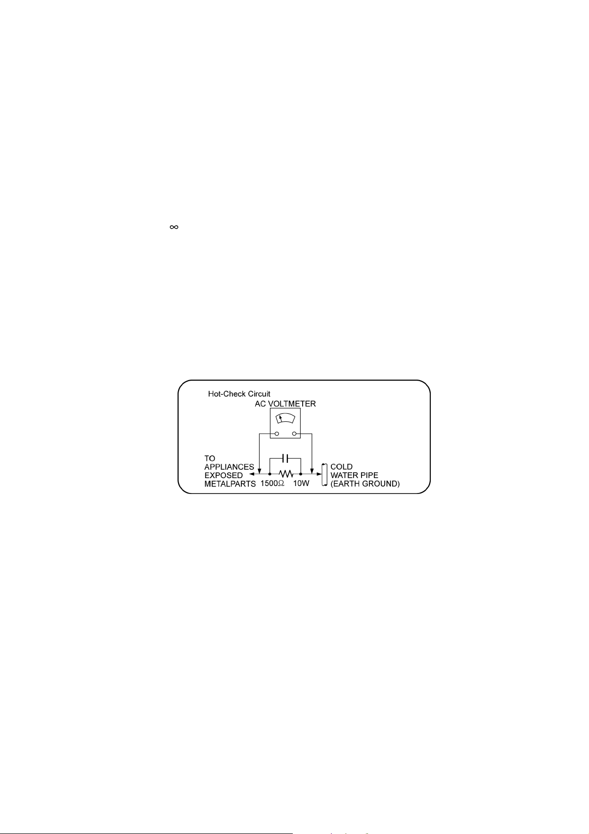
1.1.2. Leakage Current Hot Check
1. Plug the AC cord directly into the AC outlet. Do not use an isolation transformer for this check.
2. Connect a 1.5kΩ, 10 watts resistor, in parallel with a 0.15μF capacitors, between each exposed metallic part on the set and a
good earth ground such as a water pipe, as shown in Figure 1.
3. Use an AC voltmeter, with 1000 ohms/volt or more sensitivity, to measure the potential across the resistor.
4. Check each exposed metallic part, and measure the voltage at each point.
5. Reverse the AC plug in the AC outlet and repeat each of the above measurements.
6. The potential at any point should not exceed 0.75 volts RMS. A leakage current tester (Simpson Model 229 or equivalent)
may be used to make the hot checks, leakage current must not exceed 1/2 milliamp. In case a measurement is outside of the
limits specified, there is a possibility of a shock hazard, and the equipment should be repaired and rechecked before it is
returned to the customer.
Figure. 1
3
Page 4
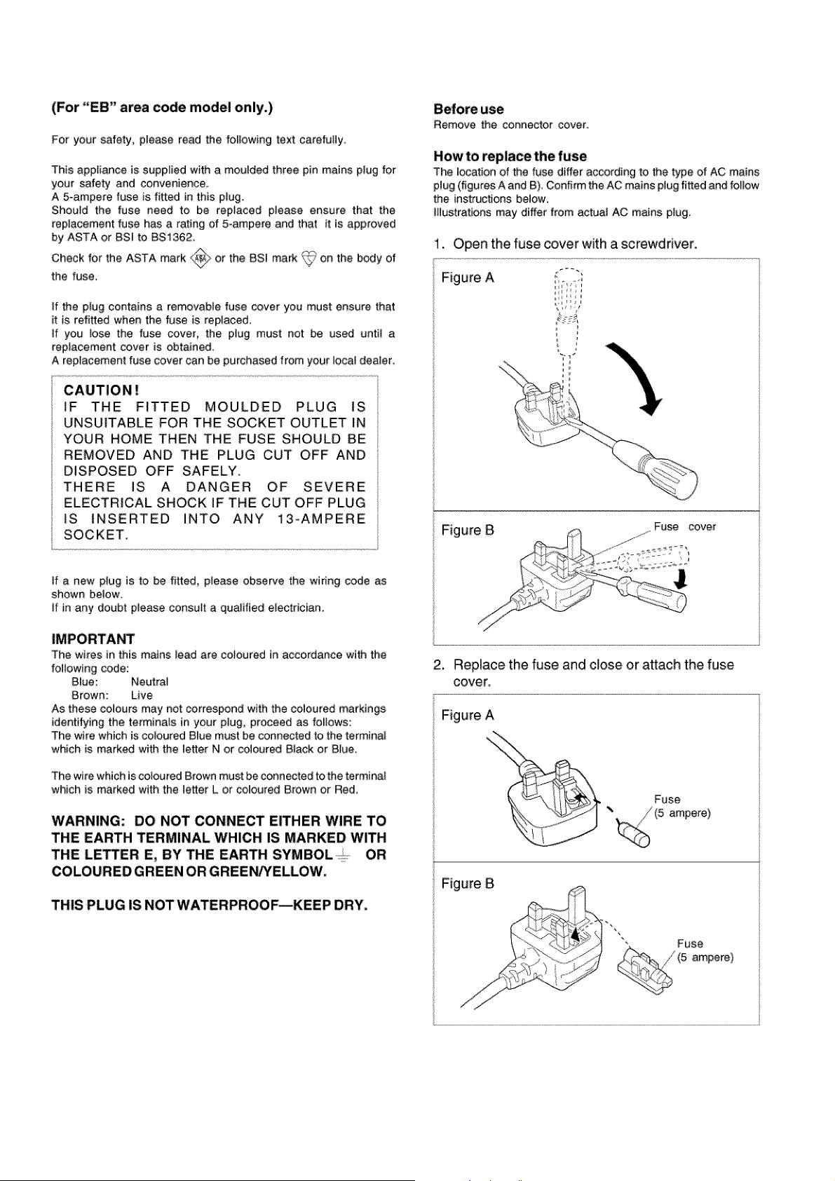
1.2. Caution for AC Cord
4
Page 5
1.3. Before Repair and Adjustment
Caution : DO NOT SHORT-CIRCUIT DIRECTLY (with a screwdriver blade, for instance), as this may destroy solid state devices.
After repairs are completed, restore power gradually using a variac, to avoid overcurrent.
• Current consumption at AC 220 - 240V, at 50Hz in NO SIGNAL mode (at volume min in FM Tuner mode) should be ~150 mA.
1.4. Protection Circuitry
The protection circuitry may have operated if either of the following conditions are noticed:
• No sound is heard when the power is turned on.
• Sound stops during a performance.
The function of this circuitry is to prevent circuitry damage if, for example, the positive and negative speaker connection wires are
"shorted", or if speaker systems with an impedance less than the indicated rated impedance of the amplifier are used.
If this occurs, follow the procedure outlines below:
1. Turn off the power.
2. Determine the cause of the problem and correct it.
3. Turn on the power once again after one minute.
Note:
When the protection circuitry functions, the unit will not operate unless the power is first turned off and then on again.
1.5. Safety Part Information
Safety Parts List:
There are special components used in this equipment which are important for safety.
These parts are marked by in the Schematic Diagrams, Exploded View & Replacement Parts List. It is essential that these
critical parts should be replaced with manufacturer’s specified parts to prevent shock, fire or other hazards. Do not modify the
original design without permission of manufacturer.
Table 1
Safety Ref. No. Part No. Part Name & Description Remarks
301 RAEX0190Z-V TRAVERSE UNIT ASS’Y (RTL)
A2 K2CZ3YY00005 AC CORD
A3 RQTX0190-B O/I BOOK (En/Sp)
A6 J0KG00000037 AC CLAMP FILTER
PCB7 REPX0708B TRANSFORMER P.C.B. (RTL)
L5901 ELF15N035AN LINE FILTER
T5901 G4CYBYY00022 TRANSFORMER
T5902 G4C2AAJ00005 SUB TRANSFORMER
Z5901 ERZVA5Z471 ZNR
RL5901 K6B1AEA00003 RELAY
F5901 K5D102BLA013 FUSE
FP5901 K5G502AA0002 FUSE PROTECTOR
JK5901 K2AA2B000011 AC INLET
5
Page 6

2Warning
2.1. Prevention of Electro Static Discharge (ESD) to Electrostatically Sensitive (ES) Devices
Some semiconductor (solid state) devices can be damaged easily by static electricity. Such components commonly are called Electrostatically Sensitive (ES) Devices. Examples of typical ES devices are integrated circuits and some field-effect transistors and
semiconductor “chip” components. The following techniques should be used to help reduce the incidence of component damage
caused by electrostatic discharge (ESD).
1. Immediately before handling any semiconductor component or semiconductor-equiped assembly, drain off any ESD on your
body by touching a known earth ground. Alternatively, obtain and wear a commercially available discharging ESD wrist strap,
which should be removed for potential shock reasons prior to applying power to the unit under test.
2. After removing an electrical assembly equiped with ES devices, place the assembly on a conductive surface such as aluminium foil, to prevent electrostatic charge build up or exposure of the assembly.
3. Use only a grounded-tip soldering iron to solder or unsolder ES devices.
4. Use only an anti-static solder remover device. Some solder removal devices not classified as “anti-static (ESD protected)” can
generate electrical charge sufficient to damage ES devices.
5. Do not use freon-propelled chemicals. These can generate electrical charges sufficient to damage ES devices.
6. Do not remove a replacement ES device from its protective package until immediately before you are ready to install it. (Most
replacement ES devices are packaged with leads electrically shorted together by conductive foam, aluminium foil or comparable conductive material).
7. Immediately before removing the protective material from the leads of a replacement ES device, touch the protective material
to the chassis or circuit assembly into which the device will be installed.
Caution :
Be sure no power is applied to the chassis or circuit, and observe all other safety precautions.
8. Minimize bodily motions when handling unpackaged replacement ES devices. (Otherwise harmless motion such as the
brushing together of your clothes fabric or the lifting of your foot from a carpeted floor can generate static electricity (ESD) suf-
ficient to damage an ES device).
6
Page 7
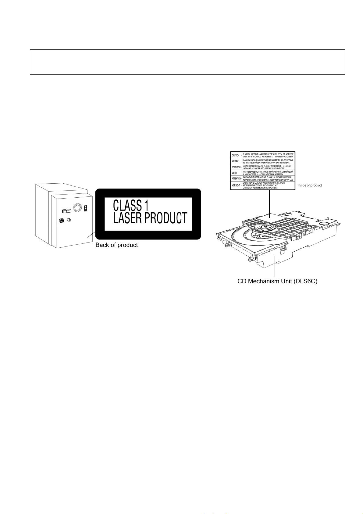
2.2. Precaution of Laser Diode
CAUTION!
THIS PRODUCT UTILIZES A LASER.
USE OF CONTROLS OR ADJUSTMENTS OR PERFORMANCE OF PROCEDURES OTHER THAN THOSE SPECIFIED HEREIN MAY RESULT
IN HAZARDOUS RADIATION EXPOSURE.
Caution:
This product utilizes a laser diode with the unit turned "on", invisible laser radiation is emitted from the pickup lens.
Wavelength: 785 nm (CD)
Maximum output radiation power from pickup: 100 μW/VDE
Laser radiation from the pickup unit is safety level, but be sure the followings:
1. Do not disassemble the pickup unit, since radiation from exposed laser diode is dangerous.
2. Do not adjust the variable resistor on the pickup unit. It was already adjusted.
3. Do not look at the focus lens using optical instruments.
4. Recommend not to look at pickup lens for a long time.
7
Page 8

2.3. Service caution based on Legal restrictions
2.3.1. General description about Lead Free Solder (PbF)
The lead free solder has been used in the mounting process of all electrical components on the printed circuit boards used for this
equipment in considering the globally environmental conservation.
The normal solder is the alloy of tin (Sn) and lead (Pb). On the other hand, the lead free solder is the alloy mainly consists of tin
(Sn), silver (Ag) and Copper (Cu), and the melting point of the lead free solder is higher approx.30 degrees C (86°F) more than that
of the normal solder.
Definition of PCB Lead Free Solder being used
The letter of “PbF” is printed either foil side or components side on the PCB using the lead free solder.
(See right figure)
Service caution for repair work using Lead Free Solder (PbF)
• The lead free solder has to be used when repairing the equipment for which the lead free solder is used.
(Definition: The letter of “PbF” is printed on the PCB using the lead free solder.)
• To put lead free solder, it should be well molten and mixed with the original lead free solder.
• Remove the remaining lead free solder on the PCB cleanly for soldering of the new IC.
• Since the melting point of the lead free solder is higher than that of the normal lead solder, it takes the longer time to melt the
lead free solder.
• Use the soldering iron (more than 70W) equipped with the temperature control after setting the temperature at 350±30 degrees
C (662±86°F).
Recommended Lead Free Solder (Service Parts Route.)
• The following 3 types of lead free solder are available through the service parts route.
RFKZ03D01K-----------(0.3mm 100g Reel)
RFKZ06D01K-----------(0.6mm 100g Reel)
RFKZ10D01K-----------(1.0mm 100g Reel)
Note
* Ingredient: Tin (Sn), 96.5%, Silver (Ag) 3.0%, Copper (Cu) 0.5%, Cobalt (Co) / Germanium (Ge) 0.1 to 0.3%
8
Page 9
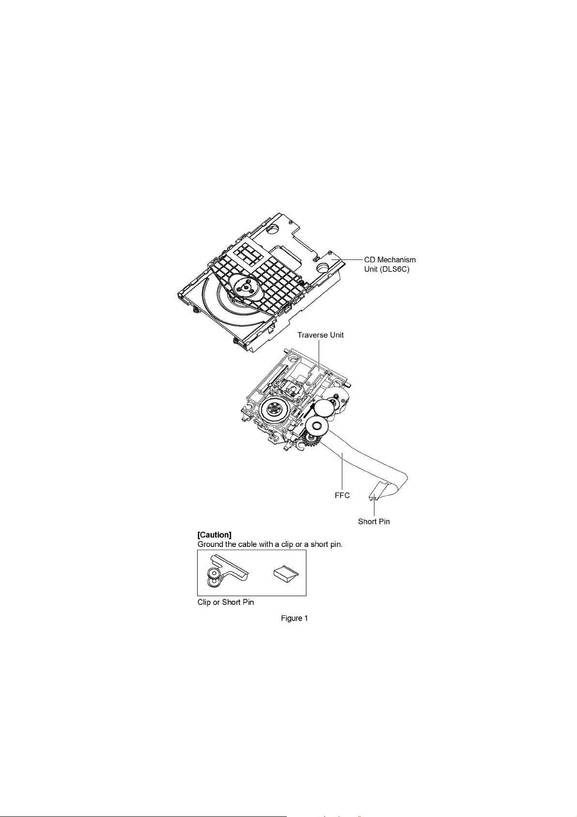
2.4. Handling Precaution for Traverse Unit
The laser diode in the optical pickup unit may break down due to static electricity of clothes or human body. Special care must be
taken avoid caution to electrostatic breakdown when servicing and handling the laser diode in the traverse unit.
2.4.1. Cautions to Be Taken in Handling the Optical Pickup Unit
The laser diode in the optical pickup unit may be damaged due to electrostatic discharge generating from clothes or human body.
Special care must be taken avoid caution to electrostatic discharge damage when servicing the laser diode.
1. Do not give a considerable shock to the optical pickup unit as it has an extremely high-precise structure.
2. To prevent the laser diode from the electrostatic discharge damage, the flexible cable of the optical pickup unit removed
should be short-circuited with a short pin or a clip.
3. The flexible cable may be cut off if an excessive force is applied to it. Use caution when handling the flexible cable.
4. The antistatic FPC is connected to the new optical pickup unit. After replacing the optical pickup unit and connecting the flexible cable, cut off the antistatic FPC.
2.4.2. Grounding for electrostatic breakdown prevention
Some devices such as the CD player use the optical pickup (laser diode) and the optical pickup will be damaged by static electricity
in the working environment. Proceed servicing works under the working environment where grounding works is completed.
2.4.2.1. Worktable grounding
1. Put a conductive material (sheet) or iron sheet on the area where the optical pickup is placed, and ground the sheet.
9
Page 10
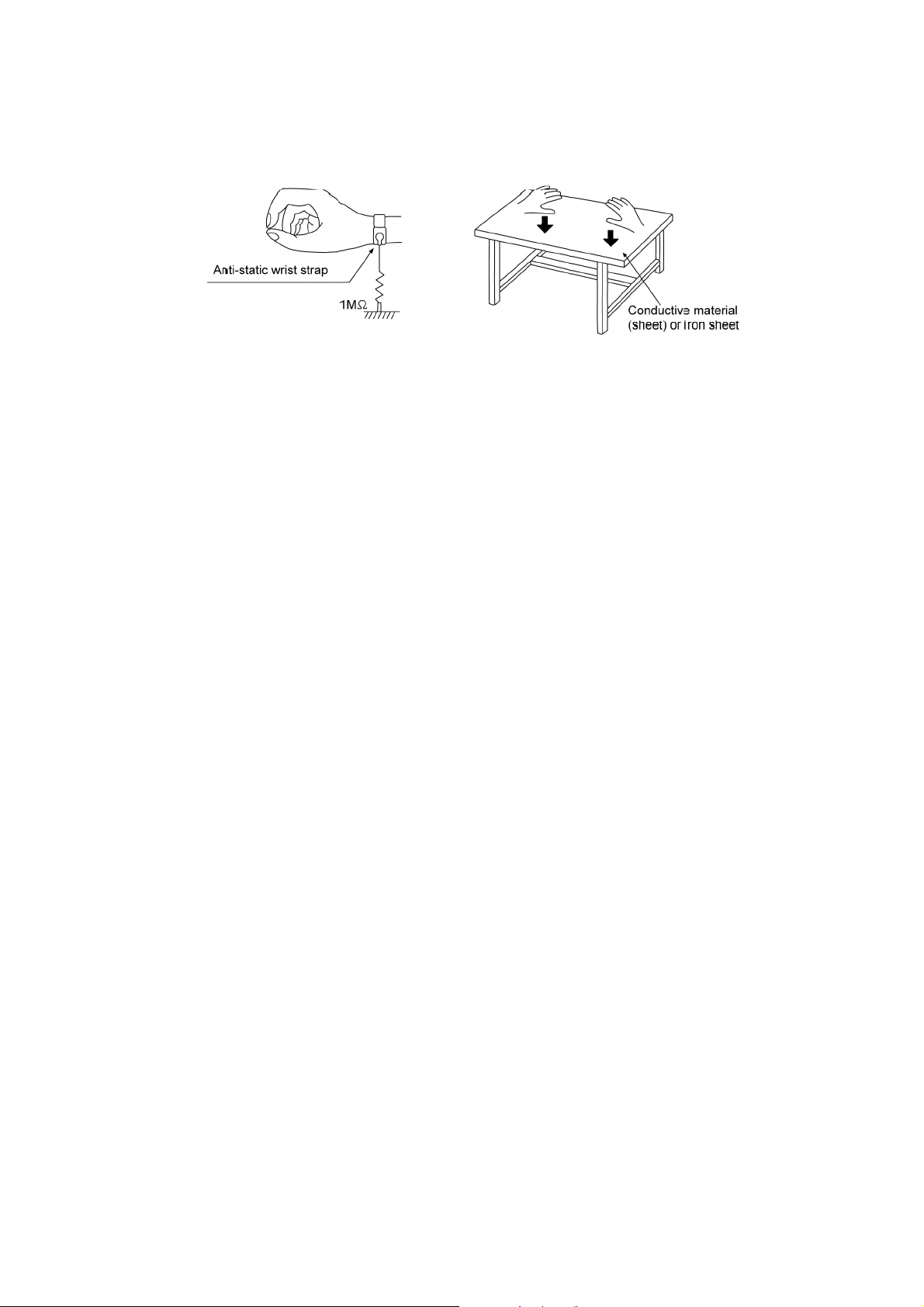
2.4.2.2. Human body grounding
1. Use the anti-static wrist strap to discharge the static electricity form your body (Figure 2).
Figure 2
10
Page 11

3 Service Navigation
3.1. Service Information
This service manual contains technical information which will allow service personnel’s to understand and service this model.
Please place orders using the parts list and not the drawing reference numbers.
If the circuit is changed or modified, this information will be followed by supplement service manual to be filed with original service
manual.
1. CD Mechanism Unit:
• This model uses CD Mechanism Unit (DLS6C).
• This service manual does not contain the following information on CD Mechanism Unit (DLS6C).
- CD Mechanism Unit P.C.B..
- Parts List for individual parts of CD Mechanism Unit (DLS6C).
- Exploded View and Part List for individual parts of CD Mechanism Unit (DLS6C).
Please refer to original service manual (Order No. MD0803034CE).
2. Micro-processor:
• Micro-processor IC, (IC800) is supplied as assembled part (RFKWMPM38DB).
11
Page 12

4 Specifications
Q Amplifier Section
RMS Output Power Stereo Mode
Front Ch (both ch driven) 20 W per channel (4 Ω),
Phone jack
Terminal Stereo, 3.5 mm
Q Tuner Section
Preset station FM 30 stations
Frequency Modulation (FM)
Frequency range 87.50 MHz to 108.00 MHz
Antenna terminals 75 Ω (unbalanced)
Q DAB Section
DAB memories 20 channels
Frequency Band (Wavelength)
Band III (UK Only) 11B to 12D
Band III (Europe) 5A to 13F
Intermediate Frequency 1st: 38.912 MHz, 2nd: 2.048 MHz
Sensitivity *BER 4x10
Max input power 0dBm
Min requirement -98dBm
Selectivity
Adjacent channel (Band III) 33dB
Far-Off channel (Band III) 45dB
DAB External Antenna
Terminal F - Connector (75 Ω)
Q CD Section
Disc played [8 cm or 12 cm]
(1) CD-Audio (CD-DA)
(2) CD-R/RW (CD-DA, MP3)
(3) MP3
Pickup
Wavelength 785 nm
Laser power CLASS I (CD)
Audio output (Disc)
Number of channels FL, FR, 2 channel
Q USB Section
Supported audio file format MP3 (*.mp3)
Maximum port power 500 mA
Q General
Power supply AC 220 to 240 V, 50 Hz
Power consumption 73 W
Dimensions (W x H x D) 153 mm x 226 mm x 292 mm
Mass 2.5 kg
Operating temperature range 0°C to +40°C
Operating humidity range 35% to 80 % RH (no condensa-
Power consumption in standby mode 0.6 W (approx)
Notes :
1. Specifications are subject to change without notices. Mass and
dimensions are approximate.
2. Total harmonic distortion is measured by the digital spectrum analyzer.
Q System : SC-PM38DBEB-K Music center: SA-PM38DBEB-K
-2
(218.640 MHz to 229.072 MHz)
(174.928 MHz to 239.200 MHz)
1 kHz, 10% THD
(50 kHz step)
tion)
Speaker: SB-PM48EG-K
12
Page 13
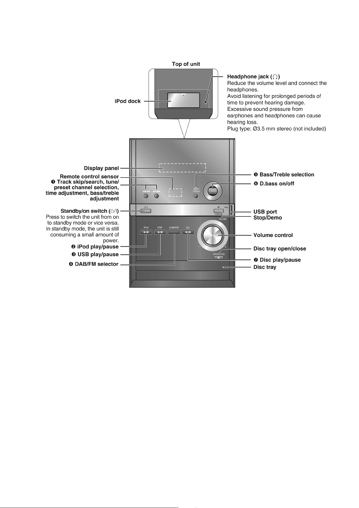
5 Location of Controls and Components
5.1. Main Unit Key Button Operations
13
Page 14
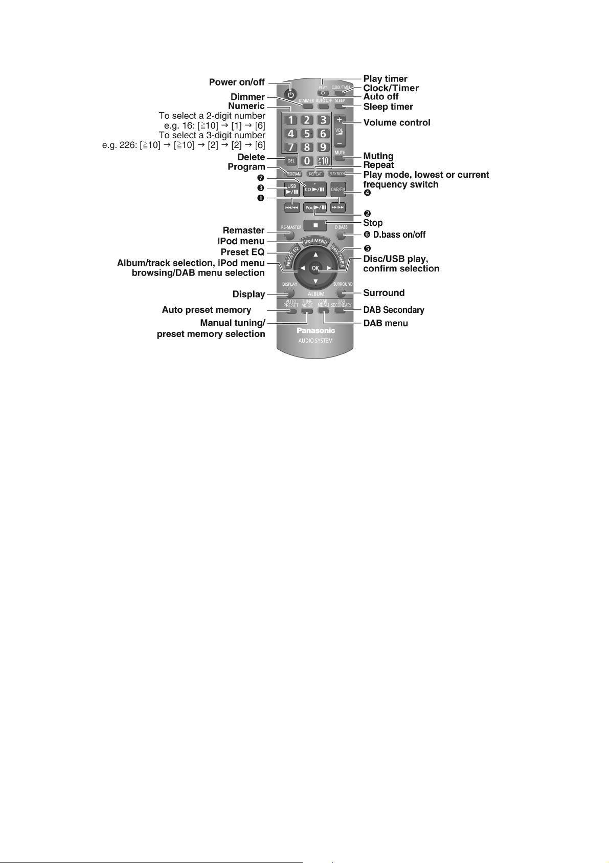
5.2. Remote Control Key Button Operations
14
Page 15

6 Operating Instructions
6.1. Disc Information
15
Page 16
7 Self diagnosis and special mode setting
This unit is equipped with features of self-diagnostic & special mode setting for checking the functions & reliability.
7.1. Service Mode Summary Table
The service modes can be activated by pressing various button combination on the main unit and remote control unit.
Below is the summary for the various modes for checking:
Player buttons Remote control unit buttons Application Note
[4], [7] To Enter into Doctor Mode for vari-
ous checking
Player buttons Remote control unit buttons Mode Name Note
Note : Applicable in Doctor Mode [DIMMER] FL Display Test (Refer to the section “7.2.2 service
[7] VOLUME setting (50dB) (Refer to the section “7.2.2 service
[8] VOLUME setting (29dB) (Refer to the section “7.2.2 service
[9] VOLUME setting (0dB) (Refer to the section “7.2.2 service
[ ], [1], [1]
[ ], [1], [2]
[ ], [1], [3]
[SLEEP] Cold Start (Refer to the section “7.2.2 service
[2] USB Test Mode (Refer to the section “7.2.2 service
CD Loading Test Mode (DLS6C) (Refer to the section “7.2.2 service
CD Traverse Unit Test Mode
(DLS6C)
CD Combination Test Mode
(DLS6C)
(Refer to the section “7.2.1 Service
Mode Table 1.)
mode Table 2 for more information.)
mode Table 2 for more information.)
mode Table 2 for more information.)
mode Table 2 for more information.)
mode Table 2 for more information.)
(Refer to the section “7.2.2 service
mode Table 2 for more information.)
(Refer to the section “7.2.2 service
mode Table 2 for more information.)
mode Table 2 for more information.)
mode Table 2 for more information.)
16
Page 17
7.2. Service Mode Table
Below is the various special modes for checking:-
7.2.1. Service Mode Table 1
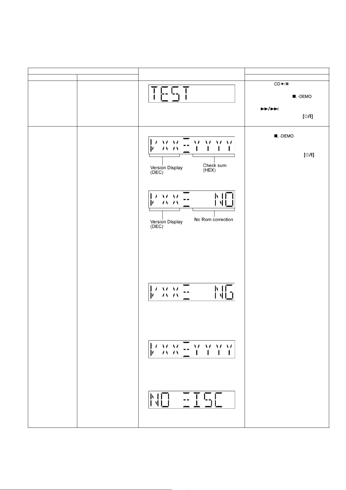
Item FL Display Key Operation
Mode Name Description Front Key
Self -Diagnostic Mode To enter into self diagnostic
checking for main unit.
Doctor Mode To enter into Doctor Mode
for checking of various
items and displaying
EEPROM and firmware version.
Note: The micro-processor
version as shown is an
example. It will be revise
when there is an updates.
FL Display sequence Display 1 → 2
(Display 1)
Checksum : (Condition 1)
1. Select [ ] for CD mode
(Ensure no CD inserted).
2. Press and hold [ ]button
for 2 seconds follow by
[].
To exit Doctor Mode, press button
on main unit or remote control.
In CD mode:
1. Press [ ] button on main
unit follow by [4] and [7] on
remote control.
To exit Doctor Mode, press button on main unit or remote control.
(a) If there is NO EEPROM header string
OR
(b) If there is no EEPROM ( no data is
received by micro-processor) [NO] is displayed.
Checksum : (Condition 2)
If the version of the EEPROM does not
match or not working properly [NG] is display.
Checksum : (Condition 3)
If the EEPROM version matches, checksum
[YYYY] is displayed.
(Display 2)
The Checksum of EEPROM and firmware
version will be display for 2 sec.
17
Page 18
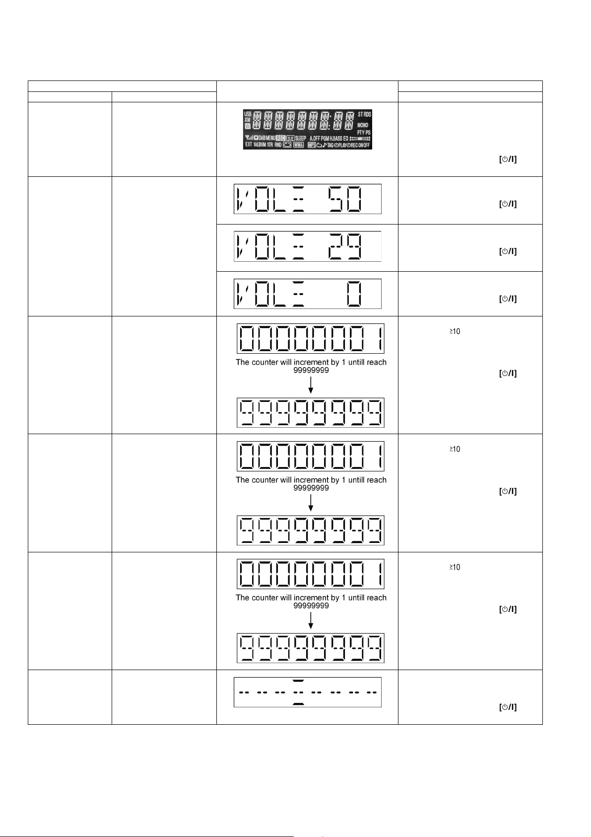
7.2.2. Service Mode Table 2
Item FL Display Key Operation
Mode Name Description Front Key
FL Display Test To check the FL segments
display (All segments will
light up)
Volume Setting To check for volume setting
CD Loading Test Mode
(DLS6C)
during this mode, Bass &
treble is set to 0dB & EQ is
switch off.
To determine the reliability of
CD Loading unit.
To check for the Open/Close
operation for the CD loading
unit. It fails when there is
abnormality in opening or
closing.
In Doctor Mode:
1. Press [DIMMER] button on
remote control.
To cancel, press [0] button on remote
control.
To exit Doctor Mode, press button on main unit or remote control.
In Doctor Mode:
1. Press [7] button on remote control.
To exit Doctor Mode, press button on main unit or remote control.
In Doctor Mode:
2. Press [8] button on remote control.
To exit Doctor Mode, press button on main unit or remote control.
In Doctor Mode:
3. Press [9] button on remote control.
To exit Doctor Mode, press button on main unit or remote control.
In Doctor Mode:
1. Press [ ], [1], [1] button on
remote control.
To cancel, press [0] button on remote
control.
To exit Doctor Mode, press button on main unit or remote control.
CD Traverse Unit Test
Mode (DLS6C)
CD Combination Test
Mode (DLS6C)
Cold Start To activate cold start upon
To check for the traverse unit
operation. In this mode, the
first & last track is access &
read. (TOC). It fails when
TOC is not completed by IOS
or the traverse is out of
focus.
A combination of CD loading
& traverse unit test.
next AC power up.
In Doctor Mode:
1. Press [ ], [1], [2] button on
remote control.
To cancel, press [0] button on remote
control.
To exit Doctor Mode, press button on main unit or remote control.
In Doctor Mode:
1. Press [ ], [1], [3] button on
remote control.
To cancel, press [0] button on remote
control.
To exit Doctor Mode, press button on main unit or remote control.
In Doctor Mode:
1. Press [SLEEP] button on remote
control.
To exit Doctor Mode, press button on main unit or remote control.
18
Page 19

Item FL Display Key Operation
Mode Name Description Front Key
USB Test Mode To Inspect USB Testing.
The display will appear after 3s,
In Doctor Mode:
1. Select to USB mode.
2. Press [2] button on remote control.
To exit Doctor Mode, press button
on main unit or remote control.
19
Page 20
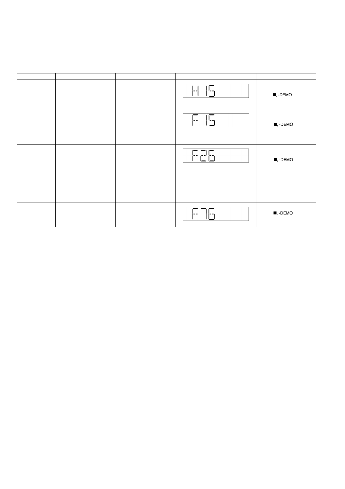
7.3. Error Code Table
Self-Diagnosis Function provides information on any problems occuring for the unit and its respective components by displaying
error codes. Thesed error code such as U**, H** and F** are stored in memory and held unless it is cleared.
The error code is automatically display after entering into self-diagnostic mode.
Error Code Diagnosis Contents Description of error Automatic FL Display Remarks
H15 CD Open SW Abnormal During normal operation
CD OPEN SW On fail to be
detected with 4 sec. Error
No. shall be clear by force
or during cold start.
F15 CD REST SW Abnormal CD traverse position intial
F26 Communication between
CD servo LSI and micro-p
abnormal.
F76 Power Amp IC output
abnormal
setting operation failsafe
counter (1000 ms) waiting
for REST SW to turn on.
Error No. shall be clear by
force or during cold start.
CD function DTMS command, after system setting, If SENSE = 'L' cannot
be detected. Memory shall
contain F26 code. After
Power on, CD function
shall continue, error disp l a y s h a l l b e " N O D I S C " .
Error No. shall be clear by
force or cold start.
DCDET1 = L (NG) For power.
For CD Mechanism Unit
(DLS6C).
Press [ ] on main
unit for next error.
For CD Mechanism Unit
(DLS6C).
Press [ ] on main
unit for next error.
For CD Mechanism Unit
(DLS6C).
Press [ ] on main
unit for next error.
Press [ ] on main
unit for next error.
20
Page 21
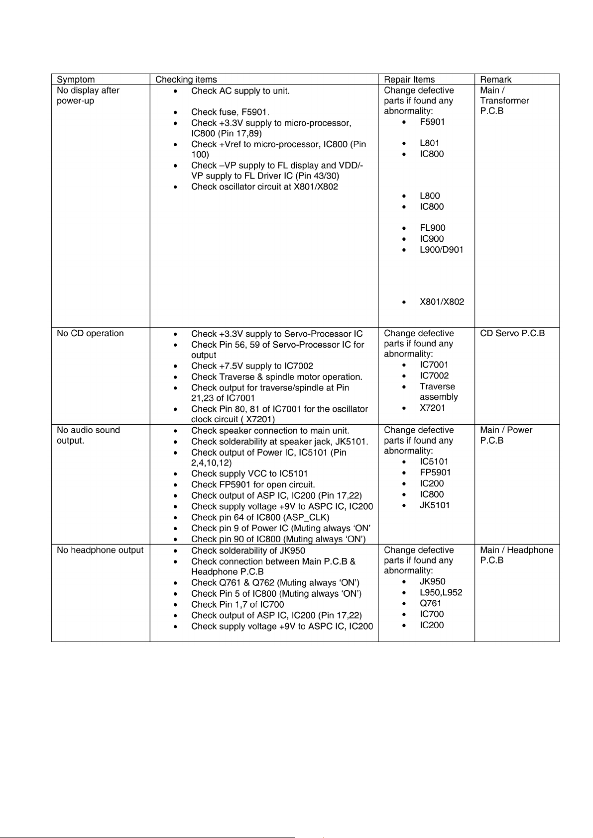
8 Troubleshooting Guide
21
Page 22

9 Service Fixture & Tools
Prepare service tools before process service position.
Service Tools Remarks
Main P.C.B. (CN901) - Panel P.C.B. (CN900) REEX1022 (11P FFC) (RTL)
22
Page 23
10 Disassembly and Assembly Instructions
“ATTENTION SERVICER”
Be careful when disassembling and servicing.
Some chassis components may have sharp edges
Special Note:
1. This section describes the disassembly procedures for all the major printed circuit boards and main components.
2. Before the disassembly process was carried out, do take special note that all safety precautions are to be carried out.
(Ensure that no AC power supply is connected during disassembling.)
3. For assembly after operation checks or replacement, reverse the respective procedures.
Special reassembly procedures are described only when required.
4. Do take note of the locators on each printed circuit board during reassembling procedures.
5. The Switch Regulator IC may have high temperature after prolonged use.
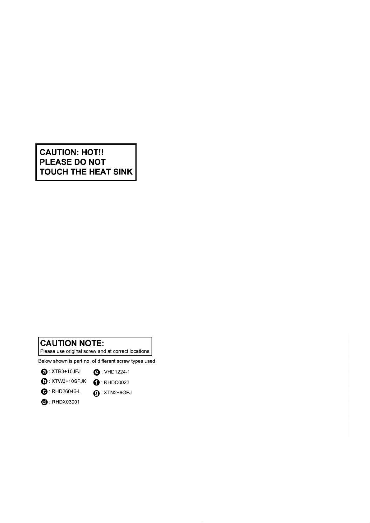
6. Use caution when removing the top cabinet and avoid touching heat sinks located in the unit.
7. Select items from the following index when checks or replacement are required.
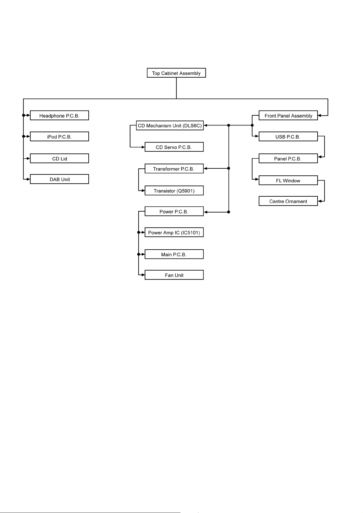
• Disassembly of Top Cabinet Assembly
• Disassembly of Headphone P.C.B.
• Disassembly of iPod P.C.B.
• Disassembly of DAB Unit P.C.B.
• Disassembly of Front Panel Assembly
• Disassembly of USB P.C.B.
• Disassembly of Panel P.C.B.
• Disassembly of FL Window
• Disassembly of Centre Ornament
• Disassembly of CD Lid
• Disassembly of CD Mechanism Unit (DLS6C)
• Disassembly of Power P.C.B.
• Replacement of Power Amp IC (IC5101)
• Disassembly of Main P.C.B.
• Disassembly of Fan Unit
• Disassembly of Transformer P.C.B.
• Replacement of Transistor (Q5901)
• Disassembly of CD Servo P.C.B.
23
Page 24
10.1. Disassembly flow chart
The following chart is the procedure for disassembling the casing and inside parts for internal inspection when carrying out the servicing.
To assemble the unit, reverse the steps shown in the chart below.
24
Page 25
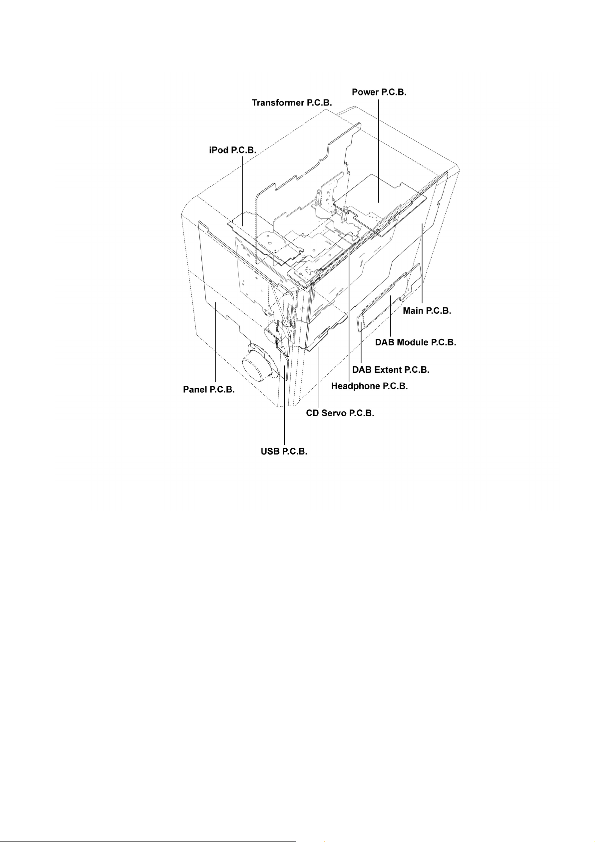
10.2. Main Parts Location Diagram
25
Page 26
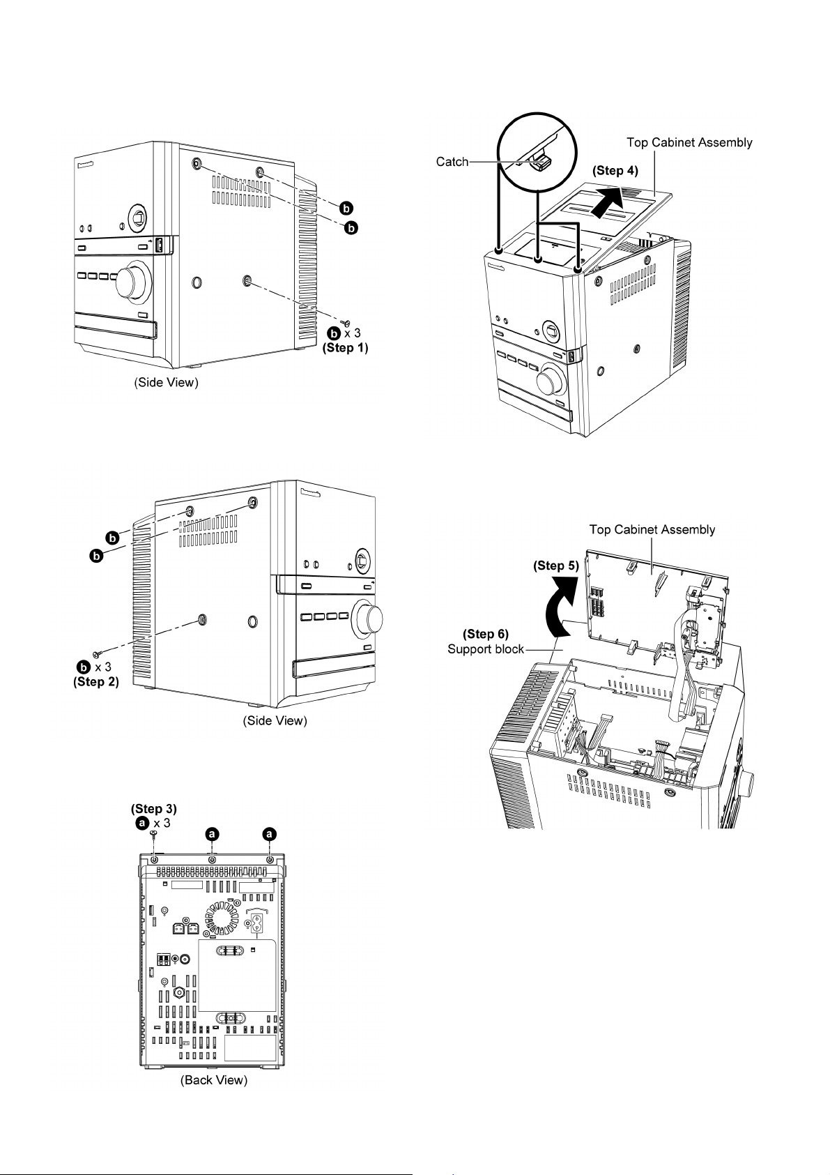
10.3. Disassembly of Top Cabinet Assembly
Step 1 : Remove 3 screws.
Step 3 : Remove 3 screws.
Step 4 : Lift the Top Cabinet Assembly as arrow shown to
release 3 catches.
Step 2 : Remove 3 screws.
Step 5 : Upset the Top Cabinet Assembly as arrow shown.
Step 6 : Place a support block underneath the Top Cabinet
Assembly.
26
Page 27
Step 7 : Detach 5P cable at connector (CN902) on Main P.C.B..
Step 8 : Detach 14P FFC at connector (CN350) on Main
P. C.B ..
Step 9 : Remove Top Cabinet Assembly.
10.4. Disassembly of Headphone P.C.B.
• Follow the (Step 1) - (Step 9) of item 10.3.
Step 1 : Remove 2 screws.
Step 2 : Release guide and remove Headphone P.C.B..
27
Page 28
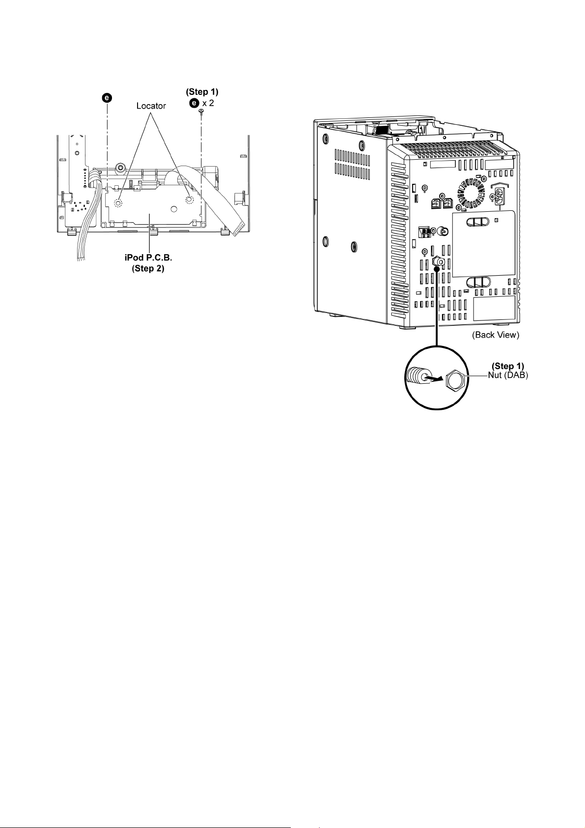
10.5. Disassembly of iPod P.C.B.
• Follow the (Step 1) - (Step 9) of item 10.3.
Step 1 : Remove 2 screws.
Step 2 : Remove iPod P.C.B..
Caution : Ensure the iPod P.C.B. is seated properly on the
locator after assembled.
10.6. Disassembly of DAB Unit P. C . B .
• Follow the (Step 1) - (Step 9) of item 10.3.
Step 1 : Remove the nut (DAB).
Caution : During reassembling, ensure Nut (DAB) is fully
tighen to the rear cabinet assembly.
28
Page 29
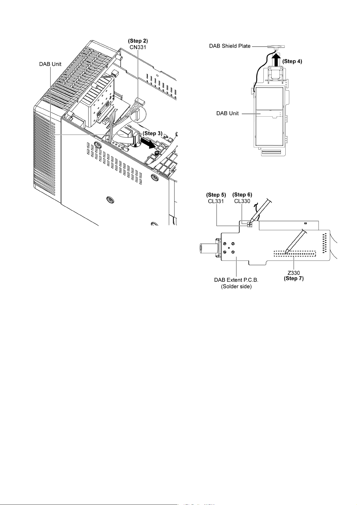
• Disassembly of DAB Extent P.C.B.
Step 4 : Remove DAB Shield Plate as arrow shown.
Step 2 : Detach 18P FFC at the connector (CN331) on Main
P. C.B ..
Step 3 : Remove DAB Unit as arrow shown.
Step 5 : Desolder point of (CL331).
Step 6 : Desolder point of (CL330).
Step 7 : Desolder points of (Z330).
29
Page 30
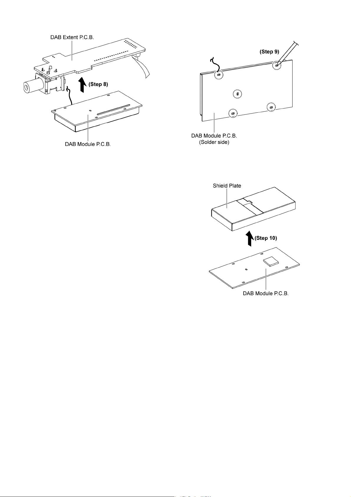
Step 8 : Remove DAB Extent P.C.B. as arrow shown.
• Disassembly of DAB Module P.C.B.
Step 9 : Desolder pins of Shield Plate.
Step 10 : Remove shield plate from DAB Module P.C.B. as
arrow shown.
30
Page 31

10.7. Disassembly of Front Panel Assembly
• Follow the (Step 1) - (Step 9) of item 10.3.
Step 1 : Detach 4P cable at connector (CN5902) on Transformer P.C.B..
Step 2 : Detach 11P FFC at connector (CN901) on Main
P. C.B ..
Step 3 : Detach 22P FFC at connector (CN380) on Main
P. C.B ..
Step 4 : Release both guides.
Step 5 : Release 3 Catches from the bottom.
Step 6 : Remove the Front Panel Assembly.
Caution : Do not attempt to exert strong force when
detaching the front panel assembly.
31
Page 32

10.8. Disassembly of USB P.C.B.
• Follow the (Step 1) - (Step 9) of item 10.3.
• Follow the (Step 1) - (Step 6) of item 10.7.
Step 1 : Remove 2 screws.
Caution : Ensure that the USB P.C.B. is firmly catched and
properly seated on the guides during assembly of the USB
P. C.B ..
Step 2 : Release both catches as arrows shown.
Step 3 : Detach the USB P.C.B as arrow shown to release from
both guides.
32
Page 33

10.9. Disassembly of Panel P.C.B.
• Follow the (Step 1) - (Step 9) of item 10.3.
• Follow the (Step 1) - (Step 6) of item 10.7.
• Follow the (Step 1) - (Step 3) of item 10.8.
Step 1 : Remove Volume Knob.
Step 3 : Release the catch
Step 4 : Remove the Panel P.C.B. as arrow shown.
Caution : During assembly ensure that Panel P.C.B. are
slot under the top guides. A ‘click’ sound will be heard
when fully catched.
Step 2 : Remove 4 screws.
33
Page 34

10.10. Disassembly of FL Window
• Follow the (Step 1) - (Step 9) of item 10.3.
• Follow the (Step 1) - (Step 6) of item 10.7.
• Follow the (Step 1) - (Step 3) of item 10.8.
• Follow the (Step 1) - (Step 4) of item 10.9.
10.11. Disassembly of Centre Ornament
• Follow the (Step 1) - (Step 9) of item 10.3.
• Follow the (Step 1) - (Step 6) of item 10.7.
• Follow the (Step 1) - (Step 3) of item 10.8.
• Follow the (Step 1) - (Step 4) of item 10.9.
• Follow the (Step 1) - (Step 2) of item 10.10.
Step 1 : Release all catches by pushing the edge of the
catches as arrows shown.
Caution : Do not apply strong force in releasing the
catches to avoid damage to the Front Panel Assembly & FL
Window.
Step 2 : Remove FL Window.
Step 1 : Release 4 catches as arrows shown.
Caution : During assembly ensure that centre ornament
are properly catched to the Front Panel Assembly.
Step 2 : Remove Centre Ornament.
34
Page 35

10.12. Disassembly of CD Lid
• Follow the (Step 1) - (Step 9) of item 10.3.
Step 2 : Move the shaft (L) of the CD Lid in the direction of
arrow shown.
Step 1 : Lift the spring out of the hook.
Caution : Keep the spring in a safe place and place it back
during assembling.
Step 3 : Move the shaft (R) of the CD Lid in the direction of
arrow shown.
Step 4 : Remove the CD Lid in the direction of arrow shown.
Caution : Do not excert strong force to the shafts during
removal and assembly of the CD Lid.
35
Page 36

10.13. Disassembly of CD Mechanism Unit (DLS6C)
• Follow the (Step 1) - (Step 9) of item 10.3.
• Follow the (Step 1) - (Step 6) of item 10.7.
Step 1 : Detach 22P FFC at connector (CN370) on Main
P. C . B . .
10.14. Disassembly of Power P.C.B.
• Follow the (Step 1) - (Step 9) of item 10.3.
• Follow the (Step 1) - (Step 6) of item 10.7.
Step 1 : Remove 1 screw.
Step 2 : Remove 2 screws.
Step 3 : Slightly tilt and remove the CD Mechanism Unit
(DLS6C) as arrow shown.
Step 2 : Detach 4P cable at connector (CN5101) on Power
P. C.B ..
Step 3 : Detach 6P cable at connector (CN200) on Main P.C.B..
36
Page 37

Step 4 : Remove 2 screws.
Step 5 : Remove Power P.C.B. as arrow shown.
10.15. Replacement of Power Amp IC (IC5101)
• Follow the (Step 1) - (Step 9) of item 10.3.
• Follow the (Step 1) - (Step 6) of item 10.7.
• Follow the (Step 1) - (Step 5) of item 10.14.
Caution : Handle the heatsink unit P.C.B. with caution due
to its high temperature after prolonged use. Touching it
may lead to injuries.
Caution 1 : Ensure the heatsink supports are seat properly.
Step 1 : Desolder pins of Power Amp IC (IC5101).
Step 2 : Remove 2 screws.
Caution 2 : Ensure the 4P wire is properly dressed into the
hook of Power P.C.B. and prevent touching the heatsink
unit.
37
Page 38

Step 3 : Remove Power Amp IC (IC5101).
• Assembly of Power Amp IC (IC5101)
Step 1 : Apply grease to the heatsink unit.
Step 2 : Install Power Amp IC onto Power P.C.B..
Caution : Ensure the pins are inserted & seated properly
on the Power P.C.B..
Step 3 : Fix the Power Amp IC (IC5101) onto the heatsink unit
with 2 screws.
Step 4 : Solder pins of the Power Amp IC (IC5101) on the solder side of Power P.C.B..
Caution : Check for solderability of the Power Amp IC.
38
Page 39

10.16. Disassembly of Main P.C.B.
• Follow the (Step 1) - (Step 9) of item 10.3.
• Follow the (Step 1) - (Step 6) of item 10.7.
• Follow the (Step 1) - (Step 5) of item 10.14.
Step 1 : Detach 2P cable at connector (CN100) on Main P.C.B..
Step 2 : Detach 22P FFC at connector (CN370) on Main
P. C.B ..
Step 3 : Detach 7P cable at connector (CN5903) on Transformer P.C.B..
Caution : Ensure the 22P FFC properly dressed into the
hook of Main P.C.B. during assembling.
Step 4 : Remove 1 screw.
39
Page 40

Step 5 : Use a paper clip to release the catch.
Step 6 : Remove Main P.C.B..
Caution : Ensure the Main P.C.B. fix onto the catches.
40
Page 41

10.17. Disassembly of Fan Unit
• Follow the (Step 1) - (Step 9) of item 10.3.
• Follow the (Step 1) - (Step 6) of item 10.7.
• Follow the (Step 1) - (Step 5) of item 10.14.
Step 1 : Remove 2 screws.
Step 3 : Release 2 catches.
Step 4 : Remove 2P cable from the holder.
Step 5 : Remove Fan Unit.
Caution : Ensure the Fan Unit is seated properly onto the
rear panel assembly.
Step 2 : Detach 2P cable at connector (CN100) on Main P.C.B..
Caution : Ensure the 2P wire is inserted into the Holder.
41
Page 42

10.18. Disassembly of Transformer P. C. B .
• Follow the (Step 1) - (Step 9) of item 10.3.
• Follow the (Step 1) - (Step 6) of item 10.7.
Step 1 : Detach 4P cable at connector (CN5101) on Power
P. C . B . .
Step 2 : Detach 7P cable at connector (CN5903) on Transformer P.C.B..
Step 4 : Place a support block to tilt the unit as shown.
Step 5 : Remove 4 screws.
Step 3 : Remove 1 screw.
Step 6 : Remove Transformer P.C.B..
Caution : Keep Transformer cover P.C.B. in safe place for
assembling use.
42
Page 43

Step 7 : Remove Transformer cover P.C.B. and Trans spacer.
Caution : Keep them in safe place for assembling use.
10.19. Replacement of Transistor (Q5901)
• Follow the (Step 1) - (Step 9) of item 10.3.
• Follow the (Step 1) - (Step 6) of item 10.7.
• Follow the (Step 1) - (Step 6) of item 10.18.
Caution : Handle the heatsink unit and P.C.B. with caution
due to its high temperature after prolonged use. Touching
it may lead to injuries .
Step 1 : Desolder pins of Transistor (Q5901).
Step 2 : Remove 1 screw.
43
Page 44

Step 3 : Remove Transistor (Q5901).
• Assembly of Transistor (Q5901)
Step 1 : Apply grease to the heatsink unit.
Step 2 : Install Transistor (Q5901) onto Transformer P.C.B..
Caution : Ensure the pins are inserted & seated properly
on Transformer P.C.B..
Step 3 : Fix the Transistor (Q5901) onto the heatsink unit with 1
screw.
Step 4 : Solder pin of the Transistor (Q5901) on the solder side
of Main P.C.B..
Caution : Check for solderability of the Transistor (Q5901).
44
Page 45

10.20. Disassembly of CD Servo P. C . B .
• Follow the (Step 1) - (Step 9) of item 10.3.
• Follow the (Step 1) - (Step 6) of item 10.7.
• Follow the (Step 1) - (Step 3) of item 10.13.
Step 5 : Detach 16P FPC at the connector (CN7001) on CD
Servo P.C.B.
Step 1 : Remove 3 screws.
Step 2 : Unsolder 4 points.
Step 3 : Move up the CD Servo P.C.B.
Step 4 : Flip the CD Servo P.C.B.
45
Page 46

11 Disassembly and Assembly of Traverse Unit
11.1. Disassembling Procedures
Step 1 : Release the guide.
Step 2 : Push the traverse slide plate (rib), ensure both grooves
are opened.
Step 3 : Slide out the traverse unit as arrow shown.
Caution : Ensure the OPU is face upwards, avoid touching
the surface of the traverse unit.
46
Page 47

11.2. Assembling Procedure
Caution : Removal of the short pin is necessary for
replacement of new traverse unit.
Step 1 : Release the guide.
Step 2 : Push the traverse slide plate (rib), ensure both grooves
are opened.
47
Page 48

Step 3 : Slot the traverse unit at approximately 45° into the
mecha chassis as arrow shown.
Caution : Ensure the bosses fix exactly onto the guides.
Step 4 : Release the guide.
Step 5 : Push the traverse slide plate (rib) to lock the traverse
unit in.
48
Page 49

12 Service Position
Note: For description of the disassembly procedures, see the Section 10
12.1. Checking & Repairing DAB Module P.C.B.
Step 1 : Remove Top Cabinet Assembly.
Step 2 : Remove DAB Unit.
Step 3 : Remove DAB Extent P.C.B..
Step 4 : Remove DAB Module P.C.B..
Step 5 : Connect DAB Module P.C.B to the DAB Extent P.C.B..
Step 9 : Connect 5P cable at connector (CN902) on Main
P. C . B . .
Step 10 : Connect 14P FFC at connector (CN350) on Main
P. C . B . .
Step 6 : Solder point of (CL331).
Step 7 : Solder point of (CL330).
Step 8 : Solder points of (Z330).
Step 11 : Lay an insulating material under the DAB unit.
49
Page 50

Step 12 : Connect 18P FFC at the connector (CN331) on Main
P. C . B . .
Step 13 : Check and repair DAB Module P.C.B. according to
the diagram shown.
12.2. Checking & Repairing USB P. C . B .
Step 1 : Remove Top Cabinet Assembly.
Step 2 : Detach 11P FFC at connector (CN901) on Main
P. C.B ..
Step 3 : Release both guides.
50
Page 51

Step 4 : Release 3 Catches.
Step 5 : Slightly remove Front Panel Assembly.
Step 6 : Remove 2 screws.
Step 10 : Connect 11P FFC at connector (CN901) on Main
P. C . B . .
Step 7 : Place a support block underneath the Top Cabinet
Assembly.
Step 8 : Connect 14P FFC at connector (CN350) on Main
P. C.B ..
Step 9 : Connect 5P cable at connector (CN902) on Main
P. C.B ..
Step 11 : Place a support block underneath the USB P.C.B..
Step 12 : Check & repair USB P.C.B. according to the diagram
shown.
51
Page 52

12.3. Checking & Repairing Panel P. C. B .
Step 1 : Remove Top Cabinet Assembly.
Step 2 : Remove Front Panel Assembly.
Step 3 : Remove USB P.C.B..
Step 4 : Remove Panel P.C.B..
Step 10 : Connect 4P cable at connector (CN5902) on Trans-
former P.C.B..
Step 11 : Connect 22P FFC at connector (CN380) on Main
P. C.B ..
Step 12 : Check & repair Panel P.C.B. according to the diagram
shown.
Step 5 : Place a support block underneath the Top Cabinet
Assembly.
Step 6 : Connect 14P FFC at connector (CN350) on Main
P. C . B . .
Step 7 : Connect 5P cable at connector (CN902) on Main
P. C . B . .
Step 8 : Lay an insulating material on Panel P.C.B..
Step 9 : Attach extension cable REEX1022 (11P FFC from
CN901 on Main P.C.B. to CN900 on Panel P.C.B.).
52
Page 53

12.4. Checking & Repairing CD Servo P.C.B.
Note : Insert CD before Checking CD Servo P.C.B.
Step 1 : Remove Top Cabinet Assembly.
Step 2 : Remove Front Panel Assembly.
Step 3 : Remove CD Mechanism Unit (DLS6C).
Step 9 : Connect 22P FFC at connector (CN370) on Main
P. C . B . .
Step 4 : Place a support block underneath the Top Cabinet
Assembly.
Step 5 : Connect 14P FFC at connector (CN350) on Main
P. C.B ..
Step 6 : Connect 5P cable at connector (CN902) on Main
P. C.B ..
Step 10 : Upset CD Mechanism Unit (DLS6C).
Step 11 : Check & repair CD Servo P.C.B. according to the dia-
gram shown.
Step 7 : Connect 11P FFC at connector (CN901) on Main
P. C.B ..
Step 8 : Connect 22P FFC at connector (CN380) on Main
P. C.B ..
53
Page 54

12.5. Checking & Repairing Power P. C. B .
Step 1 : Remove Top Cabinet Assembly.
Step 2 : Remove Front Panel Assembly.
Step 3 : Remove 1 screw.
Step 7 : Put insulating material under Power P.C.B..
Step 4 : Remove 2 screws.
Step 5 : Detach Power P.C.B..
Step 6 : Flip over Power P.C.B. as arrow shown.
Step 8 : Place a support block underneath the Top Cabinet
Assembly.
Step 9 : Connect 14P FFC at connector (CN350) on Main
P. C.B ..
Step 10 : Connect 5P cable at connector (CN902) on Main
P. C.B ..
54
Page 55

12.6. Checking & Repairing Transformer P.C.B.
Step 1 : Remove Top Cabinet Assembly.
Step 2 : Remove Front Panel Assembly.
Step 3 : Remove USB P.C.B..
Step 4 : Remove Panel P.C.B..
Step 5 : Remove Power P.C.B..
Step 6 : Remove Main P.C.B..
Step 7 : Remove Transformer P.C.B..
Step 8 : Remove CD Mechanism Unit (DLS6C).
Step 9 : Remove Fan Unit.
Step 11 : Connect 11P FFC at connector (CN901) on Main
P. C.B ..
Step 12 : Connect 22P FFC at connector (CN380) on USB
P. C.B ..
Step 13 : Connect 4P cable at connector (CN5902) on Transformer P.C.B..
Step 10 : Place a support block as diagram shown.
Step 11 : Connect 6P cable at connector (CN200) on Main
P. C . B . .
Step 12 : Connect 22P cable at connector (CN380) on Main
P. C . B . .
Step 13 : Connect 22P cable at connector (CN370) on Main
P. C . B . .
Step 14 : Check & repair Power P.C.B. according to the dia-
gram shown.
Step 14 : Connect 4P cable at connector (CN5101) on Power
P. C . B . .
55
Page 56

Step 15 : Connect 7P cable at connector (CN5903) on Transformer P.C.B..
12.7. Checking & Repairing Main P. C . B .
• Follow (Step 1 - Step 19) of item 12.6.
Step 16 : Place on insulating material under Panel P.C.B..
Step 17 : Connect 4P cable at connector (CN5902) on Trans-
former P.C.B..
Step 18 : Attach extension cable REEX1022 (11P FFC from
CN901 on Main P.C.B. to CN900 on Panel P.C.B.).
Step 1 : Flip over Fan Unit.
Step 2 : Check & repair Main P.C.B. according to the diagram
shown.
Step 19 : Connect 2P cable (Fan Unit) at connector (CN100)
on Main P.C.B..
Step 20 : Check & repair Transformer P.C.B. according to the
diagram shown.
56
Page 57

13 Voltage Measurement & Waveform Chart
Note:
• Indicated voltage values are the standard values for the unit measured by the DC electronic circuit tester (high-impedance) with
the chassis taken as standard.
Therefore, there may exist some errors in the voltage values, depending on the internal impedance of the DC circuit tester.
• Circuit voltage and waveform described herein shall be regarded as reference information when probing defect point because it
may differ from actual measuring value due to difference of Measuring instrument and its measuring condition and product itself.
13.1. USB P.C.B.
REF NO.
MODE 1234567891011121314151617181920
CD PLAY 0.7 0.7 0.7 0 0 0 3.3 3.3 3.3 1.8 1.6 1.6 00003.33.33.30.7
STANDBY 0.7 0.7 0.7 0 0 0 3.4 3.3 3.4 1.8 1.6 1.6 00003.43.43.40.7
REF NO.
MODE 21 22 23 24 25 26 27 28 29 30 31 32 33 34 35 36 37 38 39 40
CD PLAY 0.7 0.7 0.7 0.7 0.7 0.7 0.7 0.7 0.7 0.7 0.7 0.7 0.7 0.7 0.7 0.7 0.7 3.3 0.7 0
STANDBY 0.7 0.7 0.7 0.7 0.7 0.7 0.7 0.7 0.7 0.7 0.7 0.7 0.7 0.7 0.7 0.7 0.7 3.4 0.7 0
REF NO.
MODE 41 42 43 44 45 46 47 48 49 50 51 52 53 54 55 56 57 58 59 60
CD PLAY 0.7 1.8 0.7 0 0.7 3.3 0.3 3.3 3.3 0 3.3 0.7 0 0 0.7 3.0 1.0 1.0 0 0.7
STANDBY 0.7 1.8 0.7 0 0.7 3.3 0.3 3.3 3.4 0 3.4 0.7 0 0 0.7 3.3 0 0 0 0.7
REF NO.
MODE 61 62 63 64
CD PLAY 0 1.8 0.7 3.3
STANDBY 0 1.8 0.7 3.3
IC900
IC900
IC900
IC900
SA-PM38DBEB USB P.C.B.
57
Page 58

13.2. CD SERVO P.C.B.
Y
Y
Y
Y
Y
Y
Y
Y
Y
Y
Y
Y
Y
Y
Ref No.
MODE 1 2 3 4 567891011121314151617181920
CD PLA
STANDB
Ref No.
MODE 21 22 23 24 25 26 27 28 29 30 31 32 33 34 35 36 37 38 39 40
CD PLA
STANDB
Ref No.
MODE 41 42 43 44 45 46 47 48 49 50 51 52 53 54 55 56 57 58 59 60
CD PLA
STANDB
Ref No.
MODE 61 62 63 64 65 66 67 68 69 70 71 72 73 74 75 76 77 78 79 80
CD PLA
STANDB
Ref No.
MODE 81 82 83 84 85 86 87 88 89 90 91 92 93 94 95 96 97 98 99 100
CD PLA
STANDB
Ref No.
MODE 1 2 3 4 567891011121314151617181920
CD PLA
STANDB
Ref No.
MODE 21 22 23 24 25 26 27 28 29 30
CD PLA
STANDB
000 0 0000000000000003.2
000 0 0000000000000000
1.6 0 1.6 1.6 1.8 0 3.2 1.5 0 0 0 1.6 1.6 2 0 1.9 1.9 0 1.7 1.7
000 0 0000000000000000
0.2 2.4 1.7 1.9 0 0 3.2 1.2 0 1.2 1.6 1.6 0.9 1.4 1.5 1.5 0 3.2 0 0
000 0 0000000000000000
000 0 003332.903.20001.63.203.21.6
000 0 0000000000000000
1.61.60 0 000000003.20000000
000 0 0000000000000000
1.601.50 000007.51.73.23.23.22.83.83.23.27.50
000 0 0000000000000000
0 0 0 0 7.1 1.6 1.6 1.6 0 0
000 0 000000
IC7001
IC7001
IC7001
IC7001
IC7001
IC7002
IC7002
Ref No.
MODE E C B
CD PLAY 3.1 2 2.4
STANDBY 0 0.1 0
Q7601
SA-PM38DBEB CD SERVO P.C.B.
58
Page 59

13.3. MAIN P.C.B. (1/2)
REF NO.
MODE 1234567891011121314151617181920
CD PLAY 0 0 4.5 0 4.5 4.5 4.5 4.5 4.5 4.5 4.5 4.5 4.5 4.5 4.5 4.5 4.5 0 3.3 3.3
STANDBY 0 0 0.5 0 0.5 0.5 0.5 0.5 0 0 0 0.5 0 0.5 0.5 0.5 0.5 0 0 0
REF NO.
MODE 21 22 23 24 25 26 27 28 29 30 31 32 33 34 35 36 37 38 39 40
CD PLAY 9 4.5 4.5 4.5 0.9 4.5 4.5 4.5 4.5 4.5 4.5 4.5 4.5 4.5 4.5 0 4.5 0 0 4.5
STANDBY 0 0 0.5 0.5 0 0.5 0 0 0 0 0 0 0 0 0.5 0 0.5 0 0 0.5
REF NO.
MODE 41 42 43 44 45 46 47 48 49 50 51 52
CD PLAY 0 4.5 0 4.5 0 4.5 4.5 0 0 4.5 0 4.5
STANDBY 0 0.5 0 0.5 000000.500
REF NO.
MODE 12345
CD PLAY 7.5 7.5 0 5 1.25
STANDBY 0.5 0.5 0 0.7 1.25
REF NO.
MODE 12345
CD PLAY 5 0 1.2 3.3 5
STANDBY 0.7 0 0 0 0.7
REF NO.
MODE 12345678
CD PLAY 4.8 0 4.8 0 4.8 0 4.8 9
STANDBY 00000000
IC200
IC200
IC200
IC600
IC601
IC700
SA-PM38DBEB MAIN P.C.B.
59
Page 60

13.4. MAIN P.C.B. (2/2)
REF NO.
MODE 1234567891011121314151617181920
CD PLAY 3.3 3.3 1.2 0 3.3 0 3.3 0 3.3 0 0 1.5 1.5 0 1 1.6 3.3 1.8 3.3 3.3
STANDBY 0000003.300001.51.501.51.53.301.83.3
REF NO.
MODE 21 22 23 24 25 26 27 28 29 30 31 32 33 34 35 36 37 38 39 40
CD PLAY 0 3.2 0 0 3.3 10001.13.32.83.303.33.31.8003.3
STANDBY 0 1.2 2 0 3.3 2 1.5 0 0 0 0 0 0 0 0 1.2 1.8 0 0 3.3
REF NO.
MODE 41 42 43 44 45 46 47 48 49 50 51 52 53 54 55 56 57 58 59 60
CD PLAY 0 3.3 3.3 0 3.3 0 3.3 3.3 0 0 0 0 00000000
STANDBY 0 3.3 3.3 00003.3000000000000
REF NO.
MODE 61 62 63 64 65 66 67 68 69 70 71 72 73 74 75 76 77 78 79 80
CD PLAY 0 3.3 00000000001.60001000
STANDBY 0 3.3 00000000001.20001.2000
REF NO.
MODE 81 82 83 84 85 86 87 88 89 90 91 92 93 94 95 96 97 98 99 100
REC 000000003.33.303.33.3002.22003.3
STANDBY 000000003.33.303.33.3001.223.303.3
REF NO.
MODE 123456
REC 0 -1.4 0 0 -1.4 0
STANDBY 0 0.7 0 0 0.7 0
IC800
IC800
IC800
IC800
IC800
Q760
REF NO.
MODE 123456
REC 0 -1.1 0 0 -1.1 0
STANDBY
REF NO.
MODE
CD PLAY
STANDBY
REF NO.
MODE
CD PLAY
STANDBY
REF NO.
MODE
CD PLAY
STANDBY
REF NO.
MODE
CD PLAY
STANDBY
000000
Q100 Q101
ECB ECB ECB ECB ECB
0 2.3 0 0 0 0.5 0 3.3 0 5.4 5.4 4.6 0 1.3 0
0 0 0 0 0 0 0 3.3 0 0 1.3 1.3 0.5 0 0.5
Q600 Q602
ECB ECB ECB ECB ECB
13.6 9 13 5.3 7 5.7 8.8 13 9 5.3 5 0 3.3 -1 3.3
0 0 0 5.3 2.6 0 0 0 0.5 0 0 0 3.3 3.3 0
ECB ECB ECB ECB ECB
3.3 -1 3.3 0 3.3 0 0 0 3.2 3.3 3.3 0 0 1.3 0
3.3 3.3 0 0 3.3 0 0 1.3 0 0 1.7 1.3 0 0.5 0
QR600
ECB
005
000
Q761
Q350
Q603 Q604
Q375
Q382
Q761
QR384Q762 Q802 QR375 QR376
SA-PM38DBEB MAIN P.C.B.
60
Page 61

13.5. PANEL P.C.B.
REF NO.
MODE 1234567891011121314151617181920
CD PLAY 00001.801.20.81.20003.3-29-29-27-27-27-24.5 -24.5
STANDBY 00000.900000001.20.70.70.70.70.70.70.7
REF NO.
MODE 21 22 23 24 25 26 27 28 29 30 31 32 33 34 35 36 37 38 39 40
CD PLAY -29 -24.5 -27 -29.5 -29.5 -29.5 -29.5 -24.5 -20 -24.5 -24.5 -27.5 -24.5 -27 -27 -27 -27 -27 -27 -27
STANDBY 0.7 0.7 0 0.7 0.7 0.7 0.7 0.7 0 0.7 0.7 0.7 0.7 0.7 0.7 0.7 0.7 0.7 0.7 0.7
REF NO.
MODE 41 42 43 44
CD PLAY -27 -27 3.3 0
STANDBY 0.7 1.1 1.2 0
IC900
IC900
IC900
SA-PM38DBEB PANEL P.C.B.
13.6. POWER P.C.B.
REF NO.
MODE 123456789101112
CD PLAY 15.2 7.1 0 7 3.3 0 0 0 2.6 7.1 0 7.1
STANDBY 0.9 00000001.2000
IC5101
SA-PM38DBEB POWER P.C.B.
13.7. TRANSFORMER P.C.B.
REF NO.
MODE 12345
CD PLAY 6 0 1.5 3.3 6
STANDBY 6.5 0 1.2 0 6.5
REF NO.
MODE
CD PLAY
STANDBY
REF NO.
MODE
CD PLAY
STANDBY
Q5901 Q5902 Q5903 Q5904
ECB ECB ECB ECB ECB
14.5 7 12 6.8 6.8 7.2 0 0 0 0 1.8 1.8 0 0 0
0.5 0.2 0.2 0 0.2 0.5 0.6 0 0 0 1.8 2 0 6 0
Q5907
ECB
6 9.2 8
6 11 6.6
IC5901
Q5905
SA-PM38DBEB TRANSFORMER P.C.B.
61
Page 62

13.8. DAB MODULE P.C.B.
Ref No.
MODE 1 2 3 4 567891011121314151617181920
CD PLAY
STANDBY 0 0 0 0 0000000000000000
Ref No.
MODE 21 22 23 24 25 26 27 28 29 30 31 32 33 34 35 36 37 38 39 40
CD PLAY
STANDBY 0 0 0 0 0000000000000000
Ref No.
MODE 41 42 43 44 45 46 47 48 49 50 51 52 53 54 55 56 57 58 59 60
CD PLAY
STANDBY 0 0 0 0 0000000000000000
Ref No.
MODE 61 62 63 64 65 66 67 68 69 70 71 72 73 74 75 76 77 78 79 80
CD PLAY
STANDBY 0 0 0 0 0000000000000000
Ref No.
MODE 1 2 3 4 5
CD PLAY
STANDBY 0 0 0 0 0
Ref No.
MODE 1 2 3 4 5678910111213141516
CD PLAY
STANDBY
01.71.73.32.21.21.200000
000 0 0001.203.300
0 0 0 3.3 1.2 0 3.3 3.2 0 0 3.2 0
0 0 3.3 3.3 1.7 1.5 0 0 0 3.3 1.2 0
0 0 3.1 5 3.3
1.3 1.6 0 1.7 3.1 0 0 0 3.3 1.8 0 1.8 0 3.3 3.3 3.3
000 0 00000000
IC1
00000003.3
IC1
0 0 1.3 1.7 1.6 0 1.2 0
IC1
00000000
IC1
3.30000000
IC3
IC4
0000
Ref No.
MODE 1 2 3 4 567891011121314151617181920
CD PLAY
STANDBY
Ref No.
MODE 21 22 23 24 25 26 27 28 29 30 31 32 33 34 35 36 37 38 39 40
CD PLAY
STANDBY
Ref No.
MODE E C B E C B E C B E C B
CD PLAY 0 1.3 0 0 1.5 1
STANDBY 0 0 0 0 0 0
1.63.32.53.300001.50.60.60.6
000 0 00000000
3.2 1.6 1.6 1.8 1.7 1.2 1.7 1.7 3.1 2.3 3.3 0 1.5 0 0 0
000 0 00000000
Q1 Q2 Q201 Q202
IC201
IC201
3.3 3.3 0
000
0 3.3 0 3.3 0 0 3.2 2.4
00000000
3.1 0 1. 6 0
00000000
0 0 1.5
000
SA-PM38DBEB DAB MODULE P.C.B.
62
Page 63

13.9. Waveform Chart
WF No. IC200 - 5,35
(PLAY)
2.28Vp-p (100usec.div)
WF No. IC200 - 42,50
(PLAY)
588mVp-p (50nsec.div)
WF No. IC800 - 13
(PLAY)
WF No. IC200 - 17,22
(PLAY)
668mVp-p (50nsec.div)
WF No. IC700 - 1,7
(PLAY)
1.48Vp-p (250usec.div)
WF No. IC800 - 15
(PLAY)
WF No. IC200 - 20
(PLAY)
2Vp-p (100nsec.div)
WF No. IC800 - 6
(PLAY)
3.44Vp-p (5usec.div)
WF No. IC800 - 16
(PLAY)
WF No. IC200 - 40,52
(PLAY)
2.24Vp-p (10msec.div)
WF No. IC800 - 12
(PLAY)
700mVp-p (50usec.div)
WF No. IC800 - 51
(PLAY)
2.48Vp-p (100nsec.div)
WF No. IC900 - 8
(PLAY)
1.2Vp-p (500usec.div)
WF No. IC7001 - 81
(PLAY)
1.2Vp-p (25nsec.div)
3.52Vp-p (50nsec.div)
WF No. IC5101 - 2,12
(PLAY)
172mVp-p (5nsec.div)
1.72Vp-p (50nsec.div)
WF No. IC5101 - 6,8
(PLAY)
112mVp-p (5nsec.div)
2.2Vp-p (50nsec.div)
WF No. IC7001 - 80
(PLAY)
3.56Vp-p (25nsec.div)
63
Page 64

14 Illustration of IC’s, Transistors and Diodes
BA5948FPE2 (28P)
C0AABB000125
5
8
4
1
B1BCCG000023
MA2J11100L
MAZ80560ML
AN17831A
C0FBBK000066 (16P)
1
2SB0621AHA
B0EAKM000117
B0EAMM000038
C0HBB0000057 (44P)
C1AB00002719 (40P)
C1AB00003013 (52P)
MN6627954AMA
(100P)
MN66721 (80P)
MNZSFB5KJM2 (64P)
RFKWMPM38DB (100P)
C0CBCBC00208 (5P)
5
1
2
4
3
B1ABDF000026
B1ADCF000001
B1ADCE000012
B1GBCFGN0016
B1GBCFJN0009
1100L
UNR21
UNR221100L
UNR521400L
MAZ80680ML
1
B1GFGCAA0001
4
5
6
3
2
1
B0BC5R6A0266
B0BC6R8A0266
C0DBGYY00089
5
1
2
3
B1BABG000007
B1BACD000018
E
C
B
UNR9211J0L
UNR91
11J0L
4
C0DAEJG00001
1
3
5
B1BCCD000019
2SC4627J0L
B1ABCF000176
B1GBCFJJ0051
B0ADFJ000004MAZ80910MLB0BC02900004
64
Page 65

15 Overall Simplified Block for PM38
NIL_BAD::63
NIR_BAD:4
TUOL_PSA:22
TUOR_PSA:71
NIL_NUT:73
NIR_NUT:3
L_BSU/DC:04
R_BSU/DC:25
NIL_EPAT:24
NIR_EPAT:05
NIL_DOPI:44
NIR_DOPI:74
LTUO_LES:53
RTUO_LES:5
CIENOHP/H
007CI
L+_TUO:01
L-_TUO:21
R+_TUO:2
R-_TUO:4
ASP Gain
CD/USB:
TAPE:
TUNER:
DAB:
IPOD:
ASP IC200
C1AB00003013
C273 / C473
5.6K
C270 / C470
6.8K
C242 / C442
0.1u
Gain = +18.0dB
Gain = -7.0dB
Gain = +40.0dB
POWER AMP IC
IC5101
AN17831A
Gain = -25.57dBC220 / C420
0.56u
R216 R416
18k
R215 / R415
1k
R2303 / R2403
4.7k
From Selector
Source
C0AABB000125
65
Page 66

16 Block Diagram
: USB SIGNAL LINE
REST SWITCH
S7201
[68]MDATA
[70]STAT
[67]MCLK
[71]BLKCK
[72]RST
[69]MLD
167
5
18
12,1310,11
122
320
9,12,13,14
9,12,13,14
3
CP701
CP1902
7
CP701
CP1902
9
CP701
CP1902
2
CP701
CP1902
11
CP701
CP1902
4
CP701
CP1902
16
CP701
CP1902
15
CP701
CP1902
14
13
CP701
CP1902
CP701
CP1902
TO MAIN(2/2)
BLOCK DIAGRAM
TO MAIN(1/2)
BLOCK DIAGRAM
MUTE
[CH1]
LEVEL
SHIFT
[CH3]
LEVEL
SHIFT
[CH4]
LEVEL
SHIFT
[CH2]
LEVEL
SHIFT
[CH1]
MUTE
[CH2]
[41]PD
[42]LD
[25]FOP
IC7002
BA5948FPE2
4CH DRIVER
IN4
27
[24]TRP
IN3
28
IN2
1
[23]TRVP
[21]SPOUT
[22]PC
IN1
3
PC2
2
VREF
PVCC1
PVCC2
VCC
26
10,19,25
D4-
17
D4+
18
D3-
15
D3+
16
D2+
14
D2-
13
M7301*
TRAVERSE
MOTOR
D1+
12
D1-
11
M7302*
SPINDLE
MOTOR
OPTICAL PICKUP P.C.B
B
FOCUS
COIL
TRACKING
COIL
T+
OPTICAL PICKUP
PHOTO DETECTOR
SEMICONDUCTOR
LASER
F+
F-
T-
<LD_SW>
PC1
4
B
B
M
M
[34]VREF
<+VREF>
<+VREF>
<+7.5V>
B
<3.3V>
B
IC7001
Q7601
LASER POWER
DRIVE
MN6627954AMA
SERVO PROCESSOR
[39]C
EEEE
EFEF
DC
AB
DC
[38]B
[35]E
[40]A
[37]D
[36]F
[56]OUTL
[47]AVDD2
[27]IODD2
[20]PRAMVDD15
[77]IODD1
[79]REGON
[82]NTEST
CD SIGNAL LCH
X7201
[81]X1
[80]X2
CN7002
CN7002
[59]OUTR
CD SIGNAL RCH
CN807
CN807
CN807
CN807
CN807
CN807
CN7002
CN7002
CN7002
CN7002
CD OPEN
SWITCH
S7202
203
CN807
CN7002
SA-PM38DBEB CD SERVO BLOCK DIAGRAM
CD SERVO P.C.B
[63]EXT1
[64]EXT2
CN7002
CN807
7,816,15
: CD AUDIO INPUT SIGNAL LINE
16.1. CD SERVO BLOCK DIAGRAM
66
Page 67

16.2. MAIN(1/2)/ PANEL/TRANSFORMER/DAB EXTENT
: FM SIGNAL LINE
: USB SIGNAL LINE
RL5901
VOLUME JOG
KEY SW
-Vp
+3.3V
REMOTE SENSOR
S900-S904,
S906-S911
X802
32KHz
[16]XO
[9]FL_CS
[7]FL_DATA
[8]FL_CLK
FL900
FL DISPLAY
SEG1~SEG17
FROM
TRANSFORMER
MUTEA
GRID1~GRID11
14-29
32-42
31
[15]XI
5
<D3.3V>
<-Vp>
[13]VDD
[43]VDD
[30]-Vp
[19]NRST
[65]ASP_DATA
[64]ASP_CLK
ASP_DATA
TUNER_LEFT
TUNER_RIGHT
ASP_CLK
[90]AMP_MUTE
MUTE_HP
HP_SW
[5]MUTE_HP
[7]HP_SW
[98]VOL_JOG1
[93]KEY2
[92]KEY1
[25]RMT
[3]FL_CS
[4]FL_DATA
[6]FL_CLK
[1]PCONT_1
[96]DCDET
Q600
VOLTAGE
REGULATOR
Q602
VOLTAGE
REGULATOR
Q603
POWER
CONTROL
Q604
QR600
Q100,Q101
POWER
CONTROL
VOLTAGE
REGULATOR
D603
X801
8MHz
[12]OSC2
[13]OSC1
INVERTER
SWITCH
Q350
Q382
LEVEL
SHIFTER
QR384
F5901
L5901
D5905,D5907
D5909,D5911
D5901~D5904
D5921-D5924
TO FL
DISPLAY
Q5903
<-VP>
VOLTAGE
REGULATOR
Q5901,Q5902
VOLTAGE
REGULATOR
Q5907
VOLTAGE
REGULATOR
Q5905
PCONT
SWITCH
Q5904
VOLTAGE
REGULATOR
<SYS3.3V>
3.3V
<+VREF>
T5901
T5902
VR900
Z900
IC900
C0HBB0000057
MICROPROCESSOR
IC800
RFKWMPM38DB
J3CCBC000022
Z300*
JK5901
AC INLET
MAIN
TRANSFORMER
SUB
TRANSFORMER
FL DRIVER
TUNER PACK
2
3
5
OUT
IN
GND
IC5901
C0DBGYY00089
VOLTAGE
REGULATOR
3
[4]OUT
[1]CTL
[2]VCC
GND
IC600
C0DAEJG00001
VOLTAGE
REGULATOR
TO MAIN(2/2)
BLOCK DIAGRAM
TO
MAIN(2/2)
BLOCK
DIAGRAM
TO MAIN(2/2)
BLOCK DIAGRAM
<SYS3.3V>
11
B
B
6,7
CN900CN901
CN901
CN901
CN901
CN900
CN900
CN900
9,10
1,2,3
7
6
CN5903
CN5903
CN600 CN5903
2
CN600
CN600
CN600
CN5903
B
PANEL P.C.B
SA-PM38DBEB MAIN(1/2)/ PANEL/TRANSFORMER/DAB EXTENT BLOCK DIAGRAM
TRANSFORMER P.C.B
MAIN P.C.B
<CD_STAT>
P901
P901
P901
P901
P901
CN380
CN380
CN380
CN380
CN380
CN380
P901
13,15 8,10
7
16
CN7002
CN7002
CN7002
CN7002
CN7002
CN7002
CN370
CN370
CN370
CN370
CN370
CN370
[40]CLOSE_L
[43]REST_SW
[41]OPEN_H
[24]USB_RST
[34]USB_SDA
[20]USB_IRQ
[36]USB_SCL
[22]TERR
[23]VERR
[21]MMOD
3,5,6,19
4,14,22
10 13
D804
D805
4
2
4
4
3
3
617
7,816,15
19
4
8,11,17,18
TO CD SERVO
BLOCK DIAGRAM
TO USB
BLOCK DIAGRAM
TO iPod
BLOCK DIAGRAM
123
CN350CN1002
CN1002
CN350
132
CN1002
CN350
411
[31]CD_MDATA
[33]CD_MCLK
[45]CD-RST
[35]CD_MLD
8,7,6,3
10,11,12,15
13,145,4
[32]STAT
[29]BLKCK
5
18
RESET
Q802
<SYS6V>
B
<M+9V>
<AMP_VCC>
B
<A9V>
B
<DAB5V>
B
<IPOD5V>
B
<USB5V>
B
5
3
CD3.3V
[1]Vin
GND
IC601
C0DBGYY00089
VOLTAGE
REGULATOR
<3.3V>
B
[26]HALT
4,17,18,20
5,6,12,15
1,9,19
[56]IPOD_PCONT
[50]TU_SDA
[52] TU_TUNED
[51] TU_CLK
[49]TU_STEREO
[77]
[76]
UART_IN
UART_OUT
<+VREF>
B
<DOCK5V>
B
SWITCH SWITCH
Q375
QR375,
QR376
<USB5V>
B
<D3.3V>
B
[59]
IPOD_DET
DC DETECT
[72]D_MPURX
[73]D_MPUTX
[74]D_MPUCLK
[69]D_PLLSCL
[70]D_PLLSDA
[71]DAB_PON
[68]D_NRFRST
[67]D_NRST
[75]D_MPUMOD
16
CN330
CN330
CN330
CN330
CN330
CN331
CN331
CN331
CN331
CN331
18
16
18
6,7,8,9
6,7,8,9,10,11
3,4
1,2,5
3
1
13,12,11,10
16,15
18,17,14
JK330
EXTERNAL
ANT
TO DAB MODULE
BLOCK DIAGRAM
1,2,5
3,4
Z330P1
P1
P1
P1
P1
Z330
Z330
Z330
Z330
DAB_LEFT
DAB_RIGHT
DAB EXTENT P.C.B
67
Page 68

16.3. MAIN(2/2)/ HEADPHONE/ iPod/ USB BLOCK DIAGRAM
: FM SIGNAL LINE
: AUDIO OUTPUT SIGNAL LINE
: USB SIGNAL LINE
[3]TU-R
[52]CD-R
SPEAKERS
+9V
+VCC
[22]L_OUT[17]R_OUT
[19]SDA
[20]SCL
[21]VCC
Q762
Q761
MUTING
SWITCH
MUTING
CONTROL
AMP_MUTE
[37]TU-L
[9]MUTE
[2]OUT_R+
[12]OUT_L+
[8]IN_L
[6]IN_R
[4]OUT_R-
[10]OUT_L-
FILTER
FILTER
CN902
CN902
CN950
CN950
CN902CN950
<A9V>
5,7
5,7
4
[1]VCC
FP5901
<AMP_VCC>
TO CD SERVO
BLOCK DIAGRAM
TO iPod
BLOCK DIAGRAM
TO DECK
BLOCK DIAGRAM
315
[40]CD-L
HP_SW
HP_MUTE
117
ASP_DATA
ASP_CLK
TUNER_LCH
TUNER_RCH
RCH
LCH
IC200
C1AB00003013
IC700
C0AABB000125
+
-
+
-
JK950
HEADPHONE
IC5101
AN17831A
JK501
LEFT CHANNEL
RIGHT CHANNEL
AUDIO SIGNAL PROCESSOR
OP-AMP(HEADPHONE)
POWER AMPLIFIER
TO MAIN(1/2)
BLOCK DIAGRAM
[4]DAB_R
[36]DAB_L
DAB_LCH
DAB_RCH
TO MAIN(1/2)
BLOCK DIAGRAM
TO MAIN(1/2)
BLOCK DIAGRAM
TO MAIN(1/2)
BLOCK DIAGRAM
CN7002
CN7002
CN370
CN370
CD SIGNAL RCH
CD SIGNAL LCH
HEADPHONE P.C.B
POWER P.C.B
MAIN P.C.B
SA-PM38DBEB MAIN(2/2)/ HEADPHONE/ iPod/ USB BLOCK DIAGRAM
3
1
CN200
CN200
CN200
CN5102
CN5102
6
CN5102
USB P.C.B
TO MAIN 1/2
BLOCK DIAGRAM
TO MAIN 1/2
BLOCK DIAGRAM
P903
USB PORT
3,5,6,19 4,17,18,20
8,11,17,18 5,6,12,15
10
[58]CD_DATA
[61]STIN
[54]STREQ
[58]TCLK
[57]CD_STAT
[64]CD_MLD
[14]NRST
[48]I2C_DATA
[47]I2C_REQ
[46]I2C_CLK
[8]CD_NRST
[56]CD_CLK
4,14,22 1,9,19
3
4
4
3
P901
P901
P901
P901
7,8,10
CN380
CN380
CN380
CN380
CN380
[4]USBD[6]USBD+
[50]VERR
[51]TERR
[15]MMOD0
<3.3V>
B
<D1.8V>
B
IC900
MNZSFB5KJM2
USB CONTROLLER
[7]VDD
[9]VDD33
[17]VPP
[38]VDD33
[49]VDD5
[10]VDDI
[42]VDDI
[62]VDDI
12MHz
X900
[11]OSCI
[12]OSCO
P901
13,15,16
[2]D+
[3]D-
[1]USB_VBUS
VSS
[35]REC_L
[5]REC_R
[50]TAPE P/BACK-R
[42]TAPE P/BACK-L
[47]IPOD_RCH
[44]IPOD_LCH
78
CN350CN1002
510
CN350CN1002
CN1303
CN1303
CN360
CN360
CN360
CN360
CN1303
49
CN1303
58
85
76
TO MAIN 1/2
BLOCK DIAGRAM
TO MAIN 2/2
BLOCK DIAGRAM
78
CN350CN1002
510
CN350CN1002
123
TX
OUT_L
OUT_R
RX
IPOD_DET
CN350CN1002
CN1002
CN350
132
CN1002
CN350
411
DOCK
FOR iPod
CN1001
iPod P.C.B
: CD AUDIO INPUT SIGNAL LINE
: iPod AUDIO INPUT SIGNAL LINE
68
Page 69

16.4. DAB MODULE BLOCK DIAGRAM
: DAB SIGNAL LINE
[53]MPUMOD
[51]MPUCLK
[50]MPURX
[49]MPUTX
[48]NRST
<NRST>
[44]NIRQ
[43]DDOWFIC
[14]VCC_VHF
[4]VCC_LBAND
[16]VCC_MIX
[17]VCC_B8
[35]SDA
[36]SCL
[9]VHF_IN
[5]Vout
3
CE
4
Vin
[10]LOUT
[11]ROUT
[1]MCLK
[5]PDN
[2]BICK
[4]LRCK
[35]MCLK
[36]SLRCK
[37]SCLK
[38]SDAT1
[3]SDTI
DAB MODULE P.C.B
SA-PM38DBEB DAB MODULE BLOCK DIAGRAM
Q2
FILTER
SWITCH
Q201
SWITCH
Q202
+B
<VCC>
AVDD
EVDD0~EVDD4
4,14,30,47,64,74
+B
<VCC>
10
Z330P1
DAC
IC4
C0FBBK000066
Z330P1
6,7,8,9,10,11
Z330 P1
3,4
[21]STBY
Z330 P1
2
P201
1
ANT
X201
[33]XTAL[7]GND
[20]PDET [19]RF_AGC
[66]MCLK24
[30]Fref_OUT
GND
+B
<VCC>
Q1
SWITCH
[16]AGC_DET
[26]D8_AGC
[3]AIN_N
[24]B8_N
[23]B8_P
FILTER
FILTER
[2]AIN_P
1
+5V
<5V>
+B
<VCC>
2
DAB BASEBAND
PROCESSOR
IC1
MN66721
DAB IF TUNER
ADC
DRAM
(3Mb)
Synchronization and
OFDM Demodulation
Output Control
Audio Decoder
De-Interleaving
&
Viterbidecoding
IC201
C1AB00002719
VOLTAGE
REGULATOR
IC3
C0CBCBC00208
Z330P1
5
TO DAB EXTENT
BLOCK DIAGRAM
TO DAB EXTENT
BLOCK DIAGRAM
11
Z330P1
P1Z330
TO DAB EXTENT
BLOCK DIAGRAM
TO DAB EXTENT
BLOCK DIAGRAM
SWITCH
69
Page 70

17 Wiring Connection Diagram
DOCK FOR iPod
16
2
.
.
.
.
.
.
.
.
.
.
.
.
.
.
.
.
.
.
.
.
.
.
.
.
.
.
16
15
1
1
21
.
.
.
.
.
.
.
.
.
.
.
.
.
.
.
.
.
.
.
.
.
.
.
.
.
.
.
.
.
.
.
.
.
.
.
.
.
.
.
.
22
2
CD SERVO P.C.B.
M7301*
(TRV MOTOR)
M7302*
(SPL MOTOR)
CN7001
CN7002
CN905
CN900
VR900
JK950
CN950
CN5101
CN5102
JK5101
CN5903
CN5901
JK5901
SOLDER SIDE
SOLDER SIDE
SOLDER SIDE
SOLDER SIDE
SOLDER SIDE
SOLDER SIDE
SOLDER SIDE
SOLDER SIDE
CN5902
T5902
(SUB-TRANSFORMER)
CAUTION
RISK OF ELECTRIC SHOCK
AC VOLTAGE LINE.
PLEASE DO NOT TOUCH THIS P.C.B.
AC220 - 240V 50Hz
AC IN ~
VOLUME
HEADPHONE
Z300*
(TUNER PACK)
CN200
CN600
CN370
CN380
CN901
CN902
CN350
CN100
P903
P901
USB PORT
CN1001
CN1002
(SIDE B)
PANEL P.C.B.
HEADPHONE P.C.B.
POWER P.C.B.
MAIN P.C.B.
F
USB P.C.B.
1
4
.
.
.
.
.
1
11
2
10
.
.
.
.
.
.
.
1
4
....
.............
...........
16
1
4
1
1
4
.
.
.
.
.
.
.
.
7
..........
1
5
12
........
...............
...............
...............
......
........
........
17
1
2
21
22
1
5
1
13
2 14
1
21
2
22
.
.
.
.
.
.
.
.
.
.
.
.
.
.
.
.
.
.
.
.
.
.
.
.
.
.
.
.
.
.
.
.
1
11
2
10
1
1
30
.................
................
14
1
21
2
22
.
.
.
.
.
.
.
.
.
.
.
.
.
.
.
.
.
.
.
.
.
.
.
.
.
.
.
.
.
.
.
TRANSFORMER P.C.B.
H
G
SPEAKER
E
iPod P.C.B.
Z900
SENSOR
T5901
(MAIN TRANSFORMER)
SOLDER SIDE
SOLDER SIDE
P201
P1
1 . . . . . . . . . . . . .18
CN330
CL330*
CL331*
1
2
Z330*
17
.
.
.
.
.
.
.
.
.
.
.
.
.
1
18
.
.
.
.
.
.
.
.
.
.
.
.
.
2
1 . . . . . . . . . . . . .18
JK330
I
DAB MODULE P.C.B.
J
DAB EXTENT P.C.B.
DAB ANT
1
17
2
16
.
.
.
.
.
.
.
.
.
.
.
.
.
.
.
.
.
.
.
.
.
.
.
.
CN331
1
2
70
Page 71

18 Schematic Diagram Notes
(All schematic diagrams may be modified at any time with
the development of new technology)
Notes:
S900:
S901:
S902:
S903: FM/AM switch.
S904:
S906:
S907:
S908:
S909:
S910: BASS/TREBLE switch.
S911: D.BASS switch.
S7201: REST switch.
S7202: CD OPEN switch.
VR900: Volume jog.
• “ * ” REF IS FOR INDICATION ONLY.
• Importance safety notice :
Components identified by ( ) mark have special characteristics important for safety.
Furthermore, special parts which have purposes of fire-retardant (resistors), high-quality sound (capacitors), low-noise
(resistors), etc. are used.
When replacing any of components, be sure to use only
manufacturer's specified parts shown in the parts list.
-DEMO switch ( / -DEMO).
CD PLAY/PAUSE switch (CD / ).
USB switch (USB / ).
iPod switch (iPod / ).
CD EJECT switch (OPEN/CLOSE ).
POWER switch ( ).
REW switch ( ).
FWD switch ( ).
• Voltage and Signal lines:
: +B Signal Line
: -B Signal Line
: CD Audio Input Signal Line
: iPod Audio Input Signal Line
: Audio Output Signal Line
: DAB/FM Signal Line
: USB Signal Line
• Capacitor values are in microfarad(μF) unless specified otherwise, F=Farad, pF=Pico-Farad
Resistance values are in ohm(Ω), unless specified otherwise, 1K=1,000Ω, 1M=1,000KΩ
71
Page 72

19 Schematic Diagram
A
A
CD SERVO CIRCUIT
SCHEMATIC DIAGRAM - 1
SA-PM38DBEB CD SERVO CIRCUIT
B
TO
MAIN CIRCUIT
(CN370)
IN SCHEMATIC
DIAGRAM - 4
: CD AUDIO INPUT SIGNAL LINE: +B SIGNAL LINE
A
B
C
D
E
F
G
H
1 2 3 4 5 6 7 8 9 10 11 12 13 14
1 2 3 4 5 6 7 8 9 10 11 12 13 14
A
B
D
E
F
H
G
C
C7223
50V4.7
50V1
C7227
MAZ80560ML
D7650
50V1
C7228
1K
R7217
C7218
0.082
820
R7212
C7217
0.1
C7225
1000P
R7218
1K
C7226
1000P
100
R7221
C7230
0.1
C7231
6.3V220
82K
R7211
0.1C7263
LB7262 0
0
0LB7264
LB7263
C7241
1000P
C7216
680P
C7244
0.015
C7102 0.47
0.1C7204
6.3V10
C7235
C7161
0.1
C7234
0.1
C7203
6.3V220
C7315
0.47
88
C7339
0.018
10K
R7328
3.3K
R7315
R7330
5.6K
10K
R7111
C7142 3300P
C7221 15P
C7222
15P
10
C7164
10C7165
C7232
6.3V220
1KR7254
470P
C7253
C7166
0.01
0.1
C7233
10R7253
R7214
470
1M
R7220
H0H169500013
X7201
S7202
CD OPEN
0.1
C7243
6
5
8
9
11
12
10
18
15
17
16
20
19
13
14
7
2
1
4
3
22
22
1
21
CN7002
S7201
REST
0.022C7107
C7155 0.1
0.1C7154
C7264 0.1
79
77
76
78
49
47
48
50
7471 7267 685655 58575251 5453 65 6661 6259 60 6463 7069 73 75
10
879
12 11
99
100
95
94
96
97
90
91
89
93
92
98
465 213
81
82
80
86
87
88
84
83
85
45
19 17 15 141618
43
23 21 20224124
39
37
33
35
34
29
30
27
26
28
32
31
36
38
25
40
42
44
13
46
MN6627954AMA
IC7001
C7601
6.3V33
4.7
R7601
C7614
6.3V100
C7670
0.1
C7626
0.1
B1ADCF000001
Q7601
5.6R7650
LASER POWER DRIVE
+
M7302*
SPINDLE MOTOR
4CH DRIVER
39
+
M7301*
TRAVERSE MOTOR
C7334
10V220
C7335
0.1
C7613 0.1
6
5
8
9
10
12
11
7
2
1
4
3
14
13
16
15
CN7001
TO
OPTICAL
PICKUP UNIT
28 (VREF)
100
R7335
10
R7336
1K
R7332
27K
R7331
6.8K
R7323
330
R7325
1K
R7327
18K
R7349
1K
R7329
C7352
0.018
C7338
0.027
1K
R7339
GND1
191817 2015 16
14 12 9 811 1013
22 233021 282724 25 26
2167
29
345
IC7002
BA5948FPE2
A. GND
LCH OUT
TX
MCLK
RST
3.3V
STAT
7.5V
MLD
LD SW
P. GND
D. GND
BLKCK
MDATA
3.3V
REST SW
LOADING
CD OPEN SW
RCH OUT
SRDATA (ST_IN)
BCLK (ST_CLK)
LRCK (ST_REQ)
[51] ARFIN
IREF
OUTR
OUTL
TX
MLD
MCLK
NRST
STAT
FLAG
PLLF
DVDD2
AVSS1
DVSS3
BLKCK
MDATA
AVDD1
PLLF0
ARFFB
[52] DSLF
[74]
SMCK
[75] PMCK
[1] A9
[2] A11
[24] TRP
SERVO PROCESSOR
[25] FOP
RFIN X2
X1
NTEST2
A
B
F
E
D
C
PD
LD
D5
D7
D8
D9
D15
D13
D11
D10
D12
D14
D6
SDRCK
DRVDD
VREF
TRVP
BA1
A0
A2
A4
A6A8A7
A5
A3
A1
A10
NWE
BA0
PC
NRAS
NCAS
PRAMVDD33
PRAMVDD15
PRAMVSS33
SPOUT
NTEST
D1
D3
D4
D0
D2
CENV
AVDD2
RFENV
AVSS2
IODD2
DVSS1
DVDD1
OSCIN
RFOUT
IODD1
DVSS2
DQSYTXT
ARFDC
NSRVMONON
EXT1 / LRCK (ST_REQ)
EXT2 / BCLK (ST_CLK)
EXT0 / SRDATA (ST_IN)
F
A
B
E
GND
T-
F-
F+
T+
LPD
VREF
LD GND
GND (GUARD)
GND (GUARD)
LD
VCC
ARFOUT
PVCC1
D4+D1-
PVCC2
NC
NCNCNC
NC
NC
NC
IN2
NC
PC1
PC2
IN1
GND
PGND1
FO GAIN
GND
IN4
IN3
VCC
VREF
PGND2
D3+D2-
D3-D2+
D1+ D4-
CTRCRS
TRV GAIN
SRVMON0
SRVMON1
TP
90
TP
TP
38TP36
TP
37
TP
TP
50
TP
51 (ARF)
TP
24
TP
19
TP
16
TP
14
TP
18
TP
4
TP
3
TP
2
TP
1
TP
87
TP86TP
10
TP
11
TP
31
TP
13
TP
9
TP
8
TP
7
TP
12
TP
17
TP
89
TP
19.1. CD SERVO CIRCUIT
72
Page 73

19.2. MAIN CIRCUIT (1/4)
B
B
MAIN CIRCUIT
SCHEMATIC DIAGRAM - 2
SA-PM38DBEB MAIN CIRCUIT
2/4
4/4
1/4
3/4
TO MAIN
SECTION (2/4)
TO MAIN
SECTION (3/4)
: +B SIGNAL LINE
P1
P1
: AUDIO OUTPUT SIGNAL LINE: CD AUDIO INPUT SIGNAL LINE : DAB/FM SIGNAL LINE: iPod AUDIO INPUT SIGNAL LINE : USB SIGNAL LINE
A
B
C
D
E
F
G
H
1 2 3 4 5 6 7 8 9 10 11 12 13 14
R421 8.2K
GND
GND
C300
220P
C301
220P
TUNER_LCH
TU_TUNED
TUNER_RCH
TU_STEREO
TU_SDA
0.1
C302
A9V
L260
J0JBC0000015
C419 0.22
C224 0.039
C424 0.039
C221 3300P
0.022C222
0.22C220
C223 0.022
3300PC421
0.022C423
0.022C422
C219 0.22
R221 8.2K
R222 6.8K
22K
R403
TUNER_RCH
CD_LCH
220P
C207
CD_RCH
220P
C407
22K
R203
TUNER_LCH
1
C213
C212 1
C208 1
1
C214
R220 6.8K
C204 1
4
3
7
5
6
1
2
9
10
8
Z300*
TU_CLK
IPOD_RCH
IPOD_GND
IPOD_LCH
R420 6.8K
C420 0.22
1C404
C412 1
1C408
A9V
R422 6.8K
0.22C425
C236 0.015
R232
33K
C235
50V4.7
C225 0.22
C226 3300P
51
49
47
45
42
43
40
41
44
46
48
50
25
20
16
15
18
19
17
23
24
21
22
26
38 3536 3032 31 2729 2834 333739
61423 552897
11 1210 13
14
C1AB00003013
IC200
IC200
C234
0.039
47R260
C442 1
22KR233
16V470C260
C261 0.1
150K
R231
R234
33K
C233
0.039
C241
4.7
4.7
C441
C232 1
C242 1
C217 1
C218 0.1
R230 4.7K
ASP_CLK
ASP_DATA
AGND
(J3CCBC000022)
TUNER PACK
[13] SE_1
NC
[1] NC
SE_2
SCL
VCC
GND
SDA
REC_L
HP_LOUT
DAB_L
MID-L1
MID-L2
TRE-L
[28] BASS-L2
BASS-L1
SE_3
R_MAX
DBB_4
DBB_3
L-OUT
L-OUT
L_MAX
[27] DBB_1
DBB_2
R-OUT
R-OUT
REC_R
DAB_R
HP_ROUT
TRE-R
MID-R2
BASS-R1
[12] BASS-R2
MID-R1
CD-R
NC
TAPE P/BACK-R
CD-L
NC
VREF
IN1_COM-
IPOD_RCH
NC
[39] NC
AUDIO SIGNAL PROCESSOR
TU-L
NC
TAPE P/BACK-L
IPOD_LCH
NC
NC
TU-R
C202 1
DAB_LCH
DAB_RCH
1C402
73
Page 74

19.3. MAIN CIRCUIT (2/4)
B
MAIN CIRCUIT
SCHEMATIC DIAGRAM - 3
SA-PM38DBEB MAIN CIRCUIT
2/4
4/4
1/4
3/4
TO MAIN
SECTION (1/4)
TO MAIN
SECTION (4/4)
P1
P1
TO
iPod CIRCUIT
(CN1002)
IN SCHEMATIC
DIAGRAM - 8
14
1
: +B SIGNAL LINE : AUDIO OUTPUT SIGNAL LINE: CD AUDIO INPUT SIGNAL LINE : DAB/FM SIGNAL LINE: iPod AUDIO INPUT SIGNAL LINE : USB SIGNAL LINE
E
15 16 17 18 19 20 21 22 23 24 25 26 27 28
A
B
D
E
F
H
G
C
DAB_5V
R108
4.7K
0K103
10KR107
C105
16V220
C110 16V10
1
2
CN100
TO FAN
3
1
2
D108
B0ADFJ000004
R602
100
Q603
Q603
B1ABDF000026
820
R603
R604
820
A9V
Q600
B1BCCG000023
D602
MA2J11100L
16V10
C600
R601
1K
D601
MAZ80910ML
VCC
M9V
R600
1K
6.3V1000
C100
R103
100
DC DETECT
DC DETECT
10V100C102
56K
R10427R105
C106
10
B1ABCF000176
Q100
56K
R102
Q101
B1ABCF000176
DC_DET
D613
C606
0.1
DC_DET
USB5V
3
12
D603
B0ADFJ000004
4.7K
R607
B0EAKM000117
D610
B0EAKM000117
D609
R606
33K
16V22
C602
12K
R608
16V22
C603
VREF+
IPOD_PCONT
POWER CONTROL
POWER CONTROL
VOLTAGE REGULATOR VOLTAGE REGULATOR
VOLTAGE REGULATOR
C605 16V10
C604 10V100
R353
220K
8
9
11
12
10
2
5
6
3
4
1
7
14
13
CN350
R352
330K
47K
R351
UNR221100L
Q350
UART_OUT
DGND
R392
100K
UART_IN
R350
100K
IPOD_ACC3.3
R394
47K
Q382
B1ADCE000012
QR384
UNR221100L
4.7K
R393
L350 J0JHC0000034
IPOD_DET
IPOD_5V
IPOD_GND
IPOD_RCH
IPOD_LCH
B0EAKM000117
D612
B0EAKM000117
D611
B0EAKM000117
QR600
UNR521400L
R609
560
B1BCCD000019
Q604
D3.3V
IPOD_5V
312
45
C0DBGYY00089
IC601
CD7.5V
D605 B0EAKM000117
4235
IC600
C0DAEJG00001
B0EAKM000117
D606
B0EAKM000117
D608
DGND
PGND
GND
D607 B0EAKM000117
FAN+
FAN-
DOCK5V
VGND
IPOD DET
DOCK_R OUT
DPORT_AGND
VBUS_DET
IPOD_CNG1
IPOD_CNG2
DOCK_L OUT
DOCK5V_GND
DO_UART_IN/RX
DO_UART_OUT/TX
IPOD ACC 3.3V
DOCK5V_GND
VCCC OUT GND
VOLTAGE REGULATOR
CTL
VIN D3.3V
CTRL NBPGND
1
INVERTER
LEVEL SHIFTER
SWITCH
16V220
C608
B1BACD000018
Q602
VOLTAGE REGULATOR
R605
270
D604
B0BC5R6A0266
C601 16V10
0.1C607
MA2J11100L
D600
74
Page 75

19.4. MAIN CIRCUIT (3/4)
B
MAIN CIRCUIT
SCHEMATIC DIAGRAM - 4
SA-PM38DBEB MAIN CIRCUIT
2/4
4/4
1/4
3/4
TO MAIN
SECTION (4/4)
TO MAIN
SECTION (1/4)
P1
P1
A
TO
CD SERVO
CIRCUIT (CN7002)
IN SCHEMATIC
DIAGRAM - 1
1
22
TO
USB CIRCUIT
(P901)
IN SCHEMATIC
DIAGRAM - 7
22
1
: +B SIGNAL LINE : AUDIO OUTPUT SIGNAL LINE: CD AUDIO INPUT SIGNAL LINE : DAB/FM SIGNAL LINE: iPod AUDIO INPUT SIGNAL LINE : USB SIGNAL LINE
F
1 2 3 4 5 6 7 8 9 10 11 12 13 14
I
J
L
M
N
P
O
K
18
R744
R762
1K
R763
1K
R724
18
MUTE_HP
UNR211100L
Q762
VREF+
HP_R
MUTING CONTROL
231
546
B1GFGCAA0001
Q761
HP_L
MUTING
R764
6.8K
1K
R751
C750
0.01
C743 10
1K
R750
R272
0
C271
6800P
R742
68K
R722
68K
100P
C722
3.9K
R470
C752
16V100
3.9K
R270
18
R743
18
R723
C745
0.01
C725
0.01
5.6K
R273
5.6K
R473
0
R472C471
6800P
IN_R
10C723
IN_L
10KR721
R720 15K
1
C7201C740
10KR741
R740 15K
100P
C724
100P
C742
100P
C744
675
24381
IC700
C0AABB000125
K470
0
A9V
C371
1000P
C370
1000P
470R371
R370 470
1KR372
CD_MLD
CD_MDATA
CD_MCLK
BLKCK
STAT
L371
J0JKB0000020
C372
1000P
D3.3V
AGND
CD_RCH
CD_LCH
6
5
8
9
11
12
10
18
15
17
16
20
19
13
14
7
2
1
4
3
22
21
CN380
6
5
8
9
11
12
10
18
15
17
16
20
19
13
14
7
2
1
4
3
22
21
CN370
R380
4.7K
UNR211100L
QR376
4.7K
R382
R381
4.7K
QR375
UNR521400L
470
R385
470
R386
USB5V
B1BCCD000019
Q375
USB_SDA
C385
16V10
DGND
100R383
REST_SW
DGND
LOADING
USB_RST
CD7.5V
CD_OPEN_SW
USB_SCL
PGND
MMOD
D3.3V
VERR
TERR
USB_IRQ
3.3KR376
CD_RST
100R375
AGND
L-OUT
R-OUT
GND
+B
OP-AMP
(HEADPHONE)
CD_R
ST_CLK
CD_L
ST_IN
CD_AGND
CD_3.3V
CD_MLD
CD_MCLK
TX (NC)
CD_MDATA
ST_REQ
USB5V
DGND
DGND
DGND
CD_DATA
CD_CLK
DGND
MMOD
D3.3V
TERR
STIN
CD_MLD
STREQ
USB_RST
STCLK
VERR
USB_IRQ
DGND
CD_RST
USB_SCL
USB_SDA
CD_STAT
PGND
STAT
CD_3.3V
BLKCK
CD_DGND
CD_RST
LD_SW/CLDCK
CD_UNLOAD
LOADING
REST_SW
CD_7.5V
SWITCH
SWITCH
SWITCH
L470
J0JBC0000019
75
Page 76

19.5. MAIN CIRCUIT (4/4)
B
MAIN CIRCUIT
SCHEMATIC DIAGRAM - 5
SA-PM38DBEB MAIN CIRCUIT
2/4
4/4
1/4
3/4
TO MAIN
SECTION (3/4)
TO MAIN
SECTION (2/4)
P1
P1
1
C
TO
PANEL CIRCUIT
(CN900)
IN SCHEMATIC
DIAGRAM - 6
TO
TRANSFORMER
CIRCUIT (CN5903)
IN SCHEMATIC
DIAGRAM - 9
TO
POWER CIRCUIT
(CN5102)
IN SCHEMATIC
DIAGRAM - 8
D
TO
HEADPHONE
CIRCUIT (CN950)
IN SCHEMATIC
DIAGRAM - 6
11
: +B SIGNAL LINE : AUDIO OUTPUT SIGNAL LINE: CD AUDIO INPUT SIGNAL LINE : DAB/FM SIGNAL LINE: iPod AUDIO INPUT SIGNAL LINE : USB SIGNAL LINE
18
1
TO
DAB EXTENT
CIRCUIT (CN330)
IN SCHEMATIC
DIAGRAM - 8
15 16 17 18 19 20 21 22 23 24 25 26 27 28
I
J
L
M
N
P
O
K
R837 1K
R842
4.7K
R840
10K
15K
R848
HP_SW
HP_L
HP_R
2
3
1
5
4
CN902
FL_DATA
FL_CLK
FL_CS
VOL_JOG1
D3.3V
KEY1
RMT
KEY2
VREF-
6
8
9
7
2
1
4
5
3
10
11
CN901
SYS3.3V
CD_OPEN_SW
REST_SW
HALT
AGND
IN_L
AMP_MUTE
DC_DET
PCONT2
IN_R
2
4
3
1
6
5
CN200
L801
G0C3R3JA0027
L800
G0C3R3JA0027
R836 100
R828 100
47K
R830
10K
R847
USB_SCL
USB_SDA
STAT
TU_SDA
TU_STEREO
LOADING
R835 100
R846 100
R845 100
R826 1K
R832 100
6.3V1000
C806
VCC
M9V
4
5
1
3
2
7
6
CN600
10K
R859
R839
10K
100R889
CD_RST
UART_IN
UART_OUT
VREF-
C862
470P
IPOD_DET
R862
10K
470P
C863
IPOD_5V
IPOD_ACC3.3
R854 100
R855 100
220
220
R852 100
R861
R860
R866 15K
R865 10K
R856 12K
TU_CLK
TU_TUNED
IPOD_PCONT
4.7KR864
4.7KR863
R857 100
ASP_CLK
ASP_DATA
D851
MA2J11100L
470KR853
R858 100
16V10
C851
VREF-
100P
C808
50V1
C809
R881
10K
Q802
B1GBCFJN0009
HP_SW
R805 4.7K
0.01C810
MA2J11100L
RESET
D800
50V1
C811
47K
R806
2
4
3
1
6
5
CN800
FOR
SOFTWARE
FL_CLK
10K
R811
FL_DATA
100R808
100
R809
R802
220K
X801
X801
H4Z8004AA001
X802
X802
H0A327200097
100
R812
100R807
C802
0.1
MUTE_HP
FL_CS
PCONT2
4.7KR813
22PC814
22PC804
18PC801
18PC803
R815 100
VERR
USB_IRQ
MMOD
TERR
RMT
USB_RST
R884
6.8K
R888
1.8K
C882
4700P
C876
560P
C877
560P
C881
220P
A9V
VDD
R883
47K
C883
10V100
KEY1
KEY2
10KR885
4.7K470 R876
R878
VREF+
1KR891
VOL_JOG1
AMP_MUTE
DC_DET
4.7K
R810
0.1
C878
220P
C812
220P
C815
220P
C813
100P
C826
100R804
100P
C800
BLKCK
PCONT1
HALT
VREF-
GND
SYS3.3V
R890 10K
CD_MCLK
CD_MLD
CD_MDATA
D827 MA2J11100L
D826 MA2J11100L
79
77
76
78
49
47
48
50
74 7172 6768 56 5558 57 52 5154 536566 6162 596064 6370 697375
10879 1211
99
100
95
94
96
97
90
91
89
93
92
98
465213
81
82
80
86
87
88
84
83
85
45
19171514 16 18
43
232120 224124
39
37
33
35
34
29
30
27
26
28
32
31
36
38
25
40
42
44
13
46
IC800
RFKWMPM38DB
HP_L
HP_R
AGND
NC
3.3V
KEY1
RMT
HP_SW
TAPE_EJECT
VOL_JOG1
KEY2
FL_CS
FL_CLK
FL_DATA
STBY3.3V
VREF-
IN1_R
DC_DET
STBY
AMP_MUTE
AGND
IN2_L
PCONT
HALT
VCC
M+9V
M_GND
SYS3.3V
SYS_GND
[75] DAB_MODE
[74] DAB_CLK
VSS
OCD_SDA
STBY_3.3V
MMOD
OCD_SCL
MICONRST
VSS
OCD_SDA
VDD
OCD_SCL
MICONRST
VSS
OCD_SDA
OCD_SCL
MICONRST
CD_MLD
NC
1.8V
NC
NC
VSS
CD_RST
TU_SDA
OPEN_H
USB_SCL
RMT
VSS
STAT
BLKCK
NC
[26] HALT
CD_MCLK
NC
NC
NC
NC
AMP_MUTE
VDD
FAN_SW
DMT
[72] DAB_RX
DAB_PCONT
DAB_TU_SDA
DAB_TU_RST
DAB_TU_SCL
UART_IN
[73] DAB_TX
PL_H
REC_H
UART_OUT
PHOTO
MOTOR_H
NC
CLOSE_L
VSS
NC
NC
NC
NC
iPod_PDET
ASP_CLK
CRTIMER
iPod_DET
iPod_ACC3.3
DEMO_SETTING
REST_SW
CD_OPEN_SW
[52] TU_TUNED
[51] TU_CLK
TU_STEREO
[53] MODEL SELECT
MODEL_SELECT
iPod_PCONT
DAB_RST
ASP_DATA
NC
VERR
USB_RST
NC
VREF+
REGION
VOL_JOG
NRST
3.3V
OSC1(8MHz)
TAPE_EJECT
OSC2(8MHz)
MMOD
[3] FL_CS
[2] PCONT2
[1] PCONT1
MICROPROCESSOR
FL_DATA/OCD_SDA
MMOD0
TERR
HP_SWNCNC
VSS
XI(32kHz)
USB_IRQ
VDD1.8V
XO(32kHz)
FL_CLK/OCD_SCL
MUTE_HP
USB_SDA
GND
KEY2
KEY1
DCDET
MK-IN2
MK-IN1
[27] DAB_DDOWFIC
CD_MDATA
GND
DAB_5V
DAB_LCH
D_DDOWFIC
D_MPURX
D_MPUCLK
D_NRST
D_PLLSDA
D_NRFRST
DAB_PON
D_PLLSCL
D_MPUMOD
D_MPUTX
DAB_RCH
C350
47P
CN331
PLL_SDA
NRST
MPUMOD
DAB_PON
RF_RST
PLL_SCL
MPURX
MPUCLK
AGND
DAB_RCH
D5V
DGND
MPUTX
DDOWFIC
DGND
NIRQ
D5V
DAB_LCH
9
7
5
2
3
1
4
6
8
17
15
13
10
12
11
14
16
18
D_MPUTX
D_MPUMOD
D_MPUCLK
C854 47P
C853
C852 220P
100P
D_MPURX
D_NRST
D_PLLSCL
DAB_PON
D_PLLSDA
D_NRFRST
D_DDOWFIC
76
Page 77

19.6. PANEL CIRCUIT and HEADPHONE CIRCUIT
C
C
PANEL CIRCUIT
D
HEADPHONE CIRCUIT
SCHEMATIC DIAGRAM - 6
SA-PM38DBEB PANEL / HEADPHONE CIRCUIT
11
B
TO
MAIN CIRCUIT
(CN901)
IN SCHEMATIC
DIAGRAM - 5
TO
TRANSFORMER
CIRCUIT (CN5902)
IN SCHEMATIC
DIAGRAM - 9
B
TO
MAIN CIRCUIT
(CN902)
IN SCHEMATIC
DIAGRAM - 5
1
: +B SIGNAL LINE : -B SIGNAL LINE
: AUDIO OUTPUT SIGNAL LINE
A
B
C
D
E
F
G
H
1 2 3 4 5 6 7 8 9 10 11 12 13 14
1 2 3 4 5 6 7 8 9 10 11 12 13 14
A
B
D
E
F
H
G
C
100P
C906
FL1
R918 1.2
FL2
L950
L950 - L952
J0JBC0000019
100K
R950
L951
L952
2
3
1
5
4
CN950
HEADPHONE
0.01
C950
GND2
-VP
FL_CS
FL_CLK
KEY1
VOL_JOG1
6
8
9
7
2
1
4
5
3
10
11
CN900
RMT
FL_DATA
D3.3V
KEY2
SYS3.3V
1
7
6
4
2
3
5
JK950
100K
R951
0.01
C951
R930
12K
R931
22K
10K
R932
10KR928
10KR929
16V10
C908
VOL_JOG1
SYS3.3V
132
Z900
B3RAC0000017
REMOTE CONTROL SENSOR
RMT
35V22
C902
GND2
G0C101JA0027
L901
2
1
4
3
CN905
100P
C907
EVEKE2F2524B
VOLUME JOG
VR900
GND2
D3.3V
FL_CLK
G0C3R3JA0027
L900
R927
100K
1KR923
FL_DATA
1KR924
C903
0.1
C911 220P
C912 220P
GND2
C905
0.1
FL_CS
R925 1K
R926
100K
C909
35V22
C913
220P
D901
B0BC6R8A0266
68
R922
35V22
C900
FL1
16V22
C910
C901
35V22
68
R921
-VP
GND2
FL2
435612 8 3736 383231 343327 2825 26 3029 35 4039131211 15 1614910 232418 1917 21 22207 44
FL900
A2BB00000166
FL DISPLAY
S907
S908
1.2K
R908
S900
S901
1.2K
R901
2.2K
R903
4.7K
R905
3.3K
R904
5.6K
R906
S904
S903
S906
1.5K
R902
S902
SEG7
SEG7
SEG5
SEG4
SEG6
SEG6
SEG3
SEG9
SEG9
SEG8
SEG8
SEG13
SEG13
SEG16
SEG16
SEG14
SEG14
SEG15
SEG15
SEG11
SEG11
SEG10
SEG10
SEG12
SEG12
21
5
6
3
1
2
4
19
9
7
8
1617
11
10
1215 14 131820
35 37 42 44433938 414036
33
22
31
29
27
24
23
26
25
28
30
32
34
IC900
C0HBB0000057
S909
4.7K
R912
3.3K
R911
S910
S911
2.2K
R910
SEG2
SEG1
SEG17
GRID11
GRID11
GRID9
GRID9
GRID8
GRID10
GRID10
GRID7
GRID6
GRID5
GRID4
GRID3
GRID2
GRID1
1.5K
R909
CD PLAY/PAUSE
-DEMO POWER
GRID6
GRID5
[33] GRID10
GRID9
SEG5
[23] SEG7
SEG6
SEG1
-VP
SEG2
SEG3
[32] GRID11 [1] NC
SEG17
SEG17
SEG4
SEG5
SEG1
SEG2
SEG3
SEG4
GRID7
GRID8
FM/AM
FWDUSB
BASS/TREBLE
iPod D.BASS
SEG11
SEG12
SEG13
[22] SEG8 [12] VSS
SEG9
SEG10
GRID2
CD EJECT
SEG14
SEG15
GRID3
FL DRIVER
GRID4
REW
HP_L
HP_R
AGND
HP_SW
TAPE_EJECT
FL2
FL1
KEY2
3.3V
NC
VOL_JOG1
VREF-
VREF-
FL_DATA
RMT
FL_CS
-VP
GND2
FL_CLK
KEY1
VREF+
VDD
SEG16
NC
NC
FL_CLK
FL_CS
FLDATA
GRID1
GRID6
GRID5
GRID7
GRID8
GRID2
GRID3
GRID4
GRID1
NC
VSS
VDD
DOUT
OSC
NC
NC
123
77
Page 78

19.7. USB CIRCUIT
USB CIRCUIT
SCHEMATIC DIAGRAM - 7
SA-PM38DBEB USB CIRCUIT
: +B SIGNAL LINE
B
TO
MAIN CIRCUIT
(CN380)
IN SCHEMATIC
DIAGRAM - 4
: USB SIGNAL LINE
22
1
A
B
C
D
E
F
G
H
1 2 3 4 5 6 7 8 9 10 11 12 13 14
1 2 3 4 5 6 7 8 9 10 11 12 13 14
A
B
D
E
F
H
G
C
L900
G1C100K00019
C904
10
0.1
C902
0.1
C905
10
C906
0.1C901
47
C915
2.2K
R957
22K
R950
R971
1K
R972
1K
C914
0.1
C907 18P
R914
0
C908 22P
1K
R901
X900
H0A120500009
0
R904
1K
R902
15K
R955
LB951
0
C953
100
15K
R954
24R953
R952 24
2
5
G
1
4
6
G
3
P903
USB PORT
LB952
0
10
C931
0.1C952
R951
0
0.1
C951
C903
0.1
J0JBC0000033LB848
J0JBC0000033LB843
J0JBC0000033LB845
J0JBC0000033LB935
J0JBC0000033LB936
J0JBC0000033LB933
J0JBC0000033LB934
J0JBC0000033LB840
J0JBC0000033LB841
J0JBC0000033LB938
J0JBC0000033LB846
R958
100K
R903
0
LB850 0
LB852
0
6
5
8
9
11
12
10
18
15
17
16
20
19
13
14
7
2
1
4
3
22
21
P901
0
R907
LB930 0
LB932 J0JBC0000033
0
R906
0.1
C911
0.1
C912
23
58
45
44
47
48
46
303132
43
40
41
35
37
36
33
34
39
38
42
28 2526 242729
55 5650 5149 53 5452 57 62 6361
19 1820
3
2
5
4
6
8
7
1
64
15
16
9
13
10
12
11
14
1722 21
59 60
MNZSFB5KJM2
USB CONTROLLER
IC900
0.1
C913
D1.8V
DGND
NRST
P01
P04
P02
P03
P81/D8
P73/D5
P70/D2
P00
P66/D0
P72/D4
P71/D3
P75/D7
VSS
VDDI
VDD33
DGND
D1.8V
P82/D9
P77/NRE
I2C_CLK/WR_END
I2C_DATA/ERROR
I2C_REQ/WR_START
P85/D12
P86/D13
P83/D10
P84/D11
P40/D15
P87/D14
P67/D1
USB_CTRL
VPP
OCD_SDA
VDDI
OSCI
VSS
NRST
AVDD
VSS
VDD33
OSCO
MMOD0
USBNOC
USBNPP
USBD+
USBD-
PD6/IRQ3
CD_NRST
MMOD1
OCD_SCL
USB_POWER
D-
VOUT
VBUS
DGND
D5V
VBUS
D+
D-
D+
VSS
DGND
DGND
CTRL
D3.3V
VDDI
PA7
D1.8V
VSS
VERR
TERR
VDD5
STIN
D3.3V
DGND
CD_MLD
STREQ
P21/NCE0
STCLK
CD_DATA
CD_CLK
CD_STAT
PD4/NCE2
P91/SBIO
TERR
STREQ
CD_MLD
MMOD
DGND
D3.3V
M_NRST
CD_NRST
STIN
DGND
DGND
DGND
VERR
I2C_REQ
DGND
DGND
DGND
CD_STAT
STCLK
CD_DATA
CD_CLK
I2C_DATA
D5V
DGND
I2C_CLK
DGND
78
Page 79

19.8. iPod CIRCUIT, POWER CIRCUIT and DAB EXTENT CIRCUIT
iPod CIRCUIT
POWER CIRCUIT
SCHEMATIC DIAGRAM - 8
SA-PM38DBEB iPod / POWER / DAB EXTENT CIRCUIT
B
B
TO
MAIN CIRCUIT
(CN350)
IN SCHEMATIC
DIAGRAM - 3
1
14
B
TO
MAIN CIRCUIT
(CN200)
IN SCHEMATIC
DIAGRAM - 5
TO
TRANSFORMER
CIRCUIT (CN5901)
IN SCHEMATIC
DIAGRAM - 9
TO SPEAKERS
DOCK
FOR iPod
: iPod AUDIO INPUT SIGNAL LINE: +B SIGNAL LINE : DAB SIGNAL LINE: +B SIGNAL LINE
: +B SIGNAL LINE
: AUDIO OUTPUT SIGNAL LINE
DAB EXTENT CIRCUIT
TO
DAB MODULE
CIRCUIT (P1)
IN SCHEMATIC
DIAGRAM - 10
B
TO
MAIN CIRCUIT
(CN331)
IN SCHEMATIC
DIAGRAM - 5
TO
DAB MODULE
CIRCUIT (P201)
IN SCHEMATIC
DIAGRAM - 10
18
1
A
B
C
D
E
F
G
H
1 2 3 4 5 6 7 8 9 10 11 12 13 14
1 2 3 4 5 6 7 8 9 10 11 12 13 14
A
B
D
E
F
H
G
C
MA2J11100L
D5111
2
1
4
3
CN5101
C5120
1000P
FP5901
5A
R5128
10K
R5129
10K
2
4
3
1
6
5
CN5102
C5105
0.22
R5104
2.2
2.2
R5107
R5108
2.2
0.22
C5104
C5108
0.22
C5107
0.22
R5103
2.2
2
1
4
3
JK5101
R5105
100
R5101
100
MA2J11100LD5103
R5111
15K
MA2J11100L
D5102
R5112
1K
6.3V10
C5124
R5113
47K
10V3.3
C5111
C5102
1
C5106
1
1143678951 2 10 12
IC5101
C5109
470P
C5103
470P
C5113
470P
C5114
470P
R5102
22K
R5106
22K
STBY
VCC
POWER AMPLIFIER
GND_R
OUT-_R
OUT+_R
IN_R
VCC
GND
GND
AGND
IN1_R
DC_DET
IN2_L
STBY
VCC
AMP_MUTE
RCH_FULL-
LCH_FULL-
LCH_FULL+
RCH_FULL+
MUTE
GND_L
GND
IN_L
OUT_+L
AN17831A
OUT_-L
R1001 100
R1002 100
R1008
51K
R1007
51K
R1006
75K
RX
ACC_DET
TX
R1013 1K
R1009 1K
R1010 150
L1005
J0JHC0000107
J0JHC0000107
J0JHC0000107
L1007
J0JHC0000107
L1004
J0JHC0000107
L1011
ACC_ID
L1003
J0JHC0000107
USB_D-
USB_D+
0.1
C1004
USB_PWR_+5V
CHASSIS_GND
C1003
0.1
L1006
J0JHC0000107
L1010
J0JHC0000107
R1005
75K
R1004
100K
AUDIO_RETURN
L1008
IPOD_DET
L1009
6
7
5
9
25
24
26
21
20
22
17
18
13
10
12
11
16
14
15
19
23
28
27
8
1
3
4
2
29
30
CN1001
R1011
OUT_L
OUT_R
L1002
L1001
J0JHC0000107
J0JHC0000107
J0JHC0000107
PSW1
D4FB1R100009
PSW1
0.1
C1002
0.1
C1001
R1003
100K
VIDEO_COMP
R1012
0
8
9
11
12
10
2
5
6
3
4
1
7
14
13
CN1002
USB_GND
DGND
IN - R
IN - L
FW TPB+
ACC PWR
FW TPA+
FW GND
FW GND
FW TPB-
D GNDREM SENSE
RESERVED
S-VIDEO (C)
S-VIDEO (Y)
RESERVED
FW TPA -
FW PWR +12V
FW PWR +12V
DPORT_AGND
DOCK_R OUT
IPOD DET
ACC_PWR
DOCK5V_GND
DOCK5V_GND
DO_UART_IN/RX
DOCK5V
DOCK_L OUT
DO_UART_OUT/TX
IPOD ACC
VGND
VGND
VIDEO
C333
C343
9
7
5
2
3
1
4
6
8
17
15
13
10
12
11
14
16
18
CN330
CL331*
CL330*
C331
C332
C335
C334
C337
C340
C339
L347
J0JBC0000015
G0C2R2JA0027
C345
L346
4
5
132
JK330
9
7
5
2
3
1
4
6
8
17
15
13
10
12
11
14
16
18
Z330*
C347
D5V
D5V
DAB_LCH
MPURX
DGND
56P
NIRQ
330P
MPUTX
NIRQ
MPUTX
MPURX
DGND
DDOWFIC
NRST
MPUMOD
MPUCLK
RF_RST
NRST
RF_RST
MPUMOD
MPUCLK
PLL_SDA
PLL_SCL
DDOWFIC
PLL_SCL
PLL_SDA
D5V
330P
DGND
D5V
AGND
DAB_LCH
DAB_RCH
DAB_RCH
1000P
3P
0.01
DGND
1000P
AGND
330P
56P
100P
DAB_PONDAB_PON
100P
DAB ANT
2
1
RF_INPUT
RF_GND
79
Page 80

19.9. TRANSFORMER CIRCUIT
TRANSFORMER CIRCUIT
SCHEMATIC DIAGRAM - 9
SA-PM38DBEB TRANSFORMER CIRCUIT
: +B SIGNAL LINE : -B SIGNAL LINE
A
B
C
D
E
F
G
H
1 2 3 4 5 6 7 8 9 10 11 12 13 14
1 2 3 4 5 6 7 8 9 10 11 12 13 14
A
B
D
E
F
H
G
C
R5910
82
R5911
1.8K
MAZ80680ML
D5927
C5916
0.1
D5924
B0EAKM000117
B0EAKM000117
D5922
PCONT SWITCH
B0EAKM000117
D5921
22
R5915
B0EAKM000117
D5919
B0EAKM000117
D5923
16V1000
C5917
C5919
0.1
C5918
16V220
C5925
25V47
0.01
C5924
B1BABG000007
Q5907
0.1
C5910
25V1000
C5939
25V1000
C5909
-VP
100K
R5902
Q5901
0.01
VOLTAGE REGULATOR
VOLTAGE REGULATOR
VOLTAGE REGULATOR
VOLTAGE REGULATOR
C5912
2.2K
R5901
16V10
C5911
D5918
MAZ80910ML
B1ABCF000176
Q5902
820
R5903
C5923
0.01
10K
R5908
1KR5912
D5925
MA2J11100L 10K
R5909
4
5
1
3
2
7
6
CN5903
B1GBCFJJ0051
Q5904
C5922
0.01
C5920
0.1
820
R5904
D5917
MA2J11100L
3
1
2
4
5
IC5901
C0DBGYY00089
C5914
0.1
C5913
16V220
16V10
C5921
B0EAMM000038
D5901
0.1
C5928
B0EAMM000038
D5902
B0EAMM000038
D5903
B0EAMM000038
D5904
2
1
4
3
CN5901
C5901
35V3300
-VP
FL2
FL1
2
1
4
3
CN5902
0.1
C5902
B0EAKM000117
D5914
3
2
4
1
L5901
ELF15N035AN
Z5901
ERZVA5Z471
50V47
C5908
47K
R5907
SUB TRANSFORMER
4
31
2
K6B1AEA00003
RL5901
D5920
MA2J11100L
B1GBCFGN0016
Q5905
7
3
2
9
T5902
G4C2AAJ00005
B0BC02900004
D5915
12
R5905
VOLTAGE REGULATOR
B0EAKM000117
D5913
C5905
50V22
9
11
12
10
7
6
8
3
1
2
5
4
13
T5901
G4CYBYY00022
C5906
50V22
D5906
B0EAKM000117
B0EAKM000117
D5905
D5910
B0EAKM000117
D5909
B0EAKM000117
0.1
C5929
FL1
FL2
B0EAKM000117
D5908
D5907
B0EAKM000117
D5912
B0EAKM000117
B0EAKM000117
D5911
R5906
3.3K
0.01
C5907
2SB0621AHA
Q5903
B1BCCG000023
-VP
FL1
FL2
-VP(GND)
VCC
VCC
GND
GND
FL
S1
MAIN TRANSFORMER
-VP
S2
NBP
VOLTAGE REGULATOR
CRTL
OUT
IN
GND
PCONT
HALT
VCC
M+9V
M_GND
SYS3.3V
SYS_GND
220/100V
230/240V
6
TO
POWER CIRCUIT
(CN5101)
IN SCHEMATIC
DIAGRAM - 8
C
TO
PANEL CIRCUIT
(CN905)
IN SCHEMATIC
DIAGRAM - 6
B
TO
MAIN CIRCUIT
(CN600)
IN SCHEMATIC
DIAGRAM - 5
JK5901
FC5901FC5902
F5901
T1AL 250V
AC IN
220-240V
50HZ
TL
13
TL
12
TL
11
TL
10
TL
9
TL
8
TL
7
TL
5
TL
1
80
Page 81

19.10. DAB MODULE CIRCUIT
DAB MODULE CIRCUIT
SCHEMATIC DIAGRAM - 10
SA-PM38DBEB DAB MODULE CIRCUIT
: +B SIGNAL LINE : DAB SIGNAL LINE
TO
DAB EXTENT
CIRCUIT (Z330*)
IN SCHEMATIC
DIAGRAM - 8
TO
DAB EXTENT
CIRCUIT
(CL331*/CL330*)
IN SCHEMATIC
DIAGRAM - 8
A
B
C
D
E
F
G
H
1 2 3 4 5 6 7 8 9 10 11 12 13 14
1 2 3 4 5 6 7 8 9 10 11 12 13 14
A
B
D
E
F
H
G
C
TP
TP TP
TP
TP
TP
TP
TP
TP
TP
TP
TP
TP
TP
TP
TP
TP
TP
TP
TP
TP
TP
TP
TP
TP
TP
2
1
P201
RF_INPUT
C209
8P
L202
G1C18NGA0028
C2078PC206
1000P
C210
1000P
C212
1000P
C211
1000P
C214
0.1
C217
1000P
R202
10K
R215
33K
R216
10K
R201
27K
C232
0.1
Q201
UNR9111J0L
SWITCH
Q202
UNR9211J0L
SWITCH
Q1
UNR9211J0L
SWITCH
C213
1000P
C208
33P
C203 100P
C204
0.1
C231
6.3V47
C205 0.1
C202 1000P
L201
G1CR10GA0028
L203
G1CR10GA0028
RF_GND
17
34
27
26
29
30
28
25
22
23
21
24
19 2018
3132333839 37
1312 14
3
2
5
4
6
8
7
1
40
9
10
11 1615
3536
IC201
C1AB00002719
DAB IF TUNER IC
GND
AC_GND2
VCC_MIX SDA
GND
RF_AGC
VCC_B8
PDET
B8_N
0DCP
GND
XTAL
VCC_XTAL
SCL
1DCP
MUX
1DCN
REF_OUT
STBY
B8_P
D8_AGC
0DCN
CPOUT
GND
VCC_SYNTH
GND
IN02
AC_GND1
IND1
GND
NC
VDC_LDO
VHF_IN
LD0
LBAND_IN
VCC_LBAND
VTUNE
ADDR
GND
VCC_VHF
27
74
57
56
59
60
58
55
52
53
51
54
29 3028
7172737879 77
2322 24
3
2
5
4
6
8
7
1
80
9
10
21 2625
7576
IC1
IVDD1
DD0WMSC
DD0MN0
DD0MN1
DD0MN2
DD0MN3
DD0MN4
DD0MN5
SMCLK
DIAG4
DIAG5
VSS2
EVDD1
MMPUEN
VDD5
VSS7
IVDD4
VOUT
EVDD4
TSCA1
DIAG1
DIAG0
DIAG2
MPUCLK
MPUMOD
TSSYNC
TSCLK
TEST1
TEST2
DIAG6
DIAG7
VSS1
DD0DAT
DD0CLK
NADCPSC
IREF
VREFH
AINP
NADCPD
AINN
VREFL
AVDD
AVSS
ADC0YA
47
46
49
50
48
45
42
43
41
44
13
12
15
14
16
18
17
11
19
20
DAPIT
NIRQ
EVDD2
MPUTX
NRST
MPURX
SDAT2
DDOWFIC
VSS4
IVDD3
SDOCK
RDIOUT
FSY0
IVDD0
SDODT
VSS0
AGCDAT
EVDD0
NULMON
SD0WD
DDOERF
37
64
39 4038
6162636869 67
3332 34
70
31 3635
6566
SDAT1
SLRCK MCLK0
MCLK24
IVDD2
SCLK
VSS3
PWMVCXO
MCLKEN
DIAG3
EVDD3
RVSS
RVDD
VSS6
LON
C227 0.01
R208 100
R207 100
C228
0.1
C226
0.1
C225
0.1
R210
270
C224
8P
X201
X201
H0J245500084
L205 J0JBC0000019L207 J0JBC0000019
R209
27
R211
0
C223
0.1
L204
G1C91NGA0028
C233 10V10
C216 0.01
C215 0.01
C218
0.1
C219
0.1
C222
120P
C236
10P
C220
0.22
C221
0.22
C234
470P
C235
470P
C229
C2
0.1
C34
0.1
C3
0.1
C4
0.1
C5
0.1
C7
0.1
C18
100P
C19
33P
C6
0.1
C33
0.1
C25
1
R35
47K
R28
68K
R27
3.3K
C36 10V10
C38 10V10
C37 0.1
C35 0.1
R34
47K
R32
47K
R33
47K
R36
47K
C1
10V10
R205
27
R204
27
R203
1K
L208
G1CR33GA0028
L209
G1CR33GA0028
L1
J0JBC0000019L2J0JBC0000019
L210
G1CR33GA0028
R12 100
R11 100
R9 100
R1 100
R13 10K
R14 10K
R15 10K R16 10K
R17 10K
R19 1.8K
R20 1.8K
R22 8.2K
R21 8.2K
C20 1
C21 1
C23
6.3V47
R18
10
C32
330P
C24 0.1
C39 470P
C22
25V4.7
R2 100
R4 100
R23
100
R24
100
R25
100
C10 0.01
R3 100K
R5 0
R10 100
C8
0.1
C9
0.1
2
1
P1
DAB_PON
RF_RST
4
3
PLL_SCL
PLL_SDA
6
5
NRST
MPUMOD
8
7
MPUCLK
MPURX
10
9
MPUTX
NIRQ
12
11
D_DOWFIC
GND
14
13
GND
5V
16
15
5V
DAB_LCH
18
17
AGND
DAB_RCH
7
5
6
1
2
4
3
10
9
12
14
15
16
13
11
8
IC4
C0FBBK000066
DAC
Q2
2SC4627J0L
SWITCH
VSS
VDD
D1F1
VCOM
MCLK
PDN
BICK
LRCK
SDTI
TEST
DEM
DFSI
DFS0
D1F0
ROUT
LOUT
312
45
IC3
IC3
C0CBCBC00208
VOLTAGE REGULATOR
VIN
GND CE
VOUT
NC
C28
0.1
R26 100
C40 470P
C29 1
C27 1
C30 10V22
C26 6.3V47
R30
2.2K
R31
2.2K
C11
0.1
C16
1
C17
0.1
C31
0.01
C12
1000P
C13
0.01
R8
100
R6
39K
R7
1K
C15
1
C14
0.01
DAB BASEBAND PROCESSOR
MN66721
680P
81
Page 82

20 Printed Circuit Board
1
2
3
4
5
6
7
8
9
A
B
C
D
E
F
G
H
10 11 12 13
CD SERVO P.C.B. (REPX0636A)
A
SA-PM38DBEB
CD SERVO/ TRANSFORMER P.C.B.
TRANSFORMER P.C.B. (REPX0708B)
H
NOTE: " * " REF IS FOR INDICATION ONLY
0571A
0571A
B
C
E
M
M
PbF
x
x
x
x
x
x
x
x
x
x
x
x
x
x
x
x
x
x
x
x
x
x
x
x
x
x
x
x
x
x
B
C
E
B
C
E
B
C
E
B
C
E
B
C
E
B
C
E
PbF
13 12 11 10 9 8 7
53214
6
PRIMARY
SECONDARY
PRIMARY
CAUTION
RISK OF ELECTRIC SHOCK
AC VOLTAGE LINE.
PLEASE DO NOT TOUCH THIS P.C.B
AC IN
X
X
X
XXXX
X
X
C7204
C7226
R7218
C7230
R7217
R7221
C7225
R7111
R7601
C7613
C7335
R7328
R7327
R7323
R7336
R7331
R7335
IC7001
Q7601
R7211
C7218
R7212
W7001
W7013
R7349
R7650
W7006
R7325
R7339
R7329
C7339
C7338
W7024
C7352
C7217
R7332
C7243
D7650
C7253
C7315
W7008
W7012
W7011
W7004
W7005
W7007
W7010
R7253
R7254
R7220
R7214
C7222
C7221
C7166
W7021
C7154
W7002
W7003
C7107
W7025
TP2
TP18
TP19
TP16
TP13
TP1
TP9
TP4
TP10
TP37
TP39
TP36
TP14
TP3
TP38
TP28
TP90
TP50
S7201
C7241
TP31
C7142
C7216
C7233
TP11
R7330
TP8
TP87
C7155
C7102
C7161
C7244
W7009
TP12
TP17
C7234
C7626
C7264
R7315
TP24
TP88
IC7002
S7202
W7018
W7016
W7015
TP89
C7165
TP86
C7164
TP7
C7263
C7670
W7019
W7014
LB7262
LB7263
LB7264
W7017
W7026
W7020
M7301*
(TRV MOTOR)
(SPL MOTOR)
(REST SW)
C7334
C7614
C7223
C7203
C7235
C7227
CN7002
X7201
C7231
C7228
C7601
C7232
M7302*
(VREF)
(CD OPEN SW)
R5907
C5907
R5906
D5915
Q5904
C5923
R5909
R5908
R5910
R5911
C5924
D5927
C5928
C5902
C5929
C5910
D5920
IC5901
C5920C5919
C5922
C5916
Q5905
D5925
R5912
R5915
D5918
R5901
R5902
C5912
Q5902
R5903
D5917
R5904
C5914
TL5
TL1
TL7
TL8
TL9TL10
TL11
TL12
TL13
RL5901
FC5901
FC5902
L5901
Q5903
C5908
R5905
C5906
D5913
D5914
C5905
C5925
Q5907
Z5901
W5911
D5901
D5902
D5903
D5904
D5921
D5922
D5923
D5924
D5908
D5912
D5906
D5910
C5909
C5918
C5921
K5906
D5919
W5910
W5907
D5911
D5909
D5907
D5905
CN5902
CN5903
CN5901
C5901
C5917
C5913
Q5901
C5911
W5901
W5902
W5903
W5904
JK5901
W5915
W5914
W5913
W5912
W5920
W5921
W5922
W5923
W5917
W5916
W5918
W5919
W5924
K1006
0617AA-1
0617AA-1
F5901
T1AL 250V
220V - 240V
50Hz
T5902
(SUB-TRANSFORMER)
C5939
TP51
(ARF)
CN7001
(TO
OPTICAL
PICKUP
UNIT)
T5901
(MAIN TRANSFORMER)
14
50
26
30
35
40
45
76
100
95
90
85
80
25
1
5
10
15
20
51
75
70
65
60
55
1015
152029302528
22
20
21
11
22
1
2
12
18
19
16
17
14
15
12
13
10
11
8
9
6
7
4
5
2
3
1
1615
14
13
12
11
10
9
7
8
5
6
3
4
1
2
4
3
2
1
2
3
6
9
7
12
34
1
4
17
1
4
654 32
3
2
3
2
8
1
2
3
45
20.1. CD SERVO P.C.B. and TRANSFORMER P.C.B.
82
Page 83

20.2. MAIN P.C.B., DAB MODULE P.C.B. and DAB EXTENT P.C.B.
1
2
3
4
5
6
7
8
9
A
B
C
D
E
F
G
H
10 11 12 13
SA-PM38DBEB
MAIN/ DAB MODULE/ DAB EXTENT P.C.B.
MAIN P.C.B. (REPX0708B)
B
NOTE: " * " REF IS FOR INDICATION ONLY
DAB MODULE P.C.B. (RFKB4246A)
I
DAB EXTENT P.C.B. (REPX0708B)
J
3223A-1
3223A-1
B
C
E
B
C
E
B
C
E
B
C
E
B
C
E
2
3
1
B
C
E
B
C
E
1
3
2
B
C
E
B
C
E
B
C
E
B
C
E
B
C
E
B
C
E
PbF
B
C
E
PbF
PbF
B
C
E
0617AC-1
0617AC-1
IC600
C235
C260
R260
CN800
(FOR SOFTWARE)
X802
C809
C811
C806
L800
L801
C851
L371
J372
D605
D607
D608
D606
C602
C603
C604
D611
D612
C605
C600
Q600
D609
D610
D613
Q604
Z300*
(TUNER PACK)
W5699
W5697
W5674
R105
C105
C102
IC700
W5606
W5645
W5641
W5642
W5644
W5643
W5676
W5675
W5617
W5611
W5610
W5662
W5663
W5636
W5656
W5668
W5635
W5664
W5624
W5600
W5626
W5619
W5614
W5646
W5647
W5648
W5696
W5690
W5652
W5651
W5627
W5634
W5633
W5629
W5632
W5650
W5613
W5631
W5609
W5612
W5608
W5621
W5622
W5602
W5605
W5607
W5604
W5618
W5603
W5615
W5601
W5658
W5657
W5661
W5640
W5637
W5638
W5660
W5671
W5653
W5673
W5665
W5659
W5669
W5666
W5683
W5628
W5686
W5685
W5639
CN901
X801
W5625
W5620
W5688
W5623
W5689
W5680
W5691
W5684
W5694
W5682
W5692
W5693
W5701
W5672
W5677
W5678
W5679
W5616
W5630
W5654
W5681
W5700
W5695
W5687
CN370
CN380
W6025
W6026
W6027
W6028
W6029
W6030
W6031
W6032
W6033
W6034
W6035
W6036
W6037
C752
C883
CN200
CN350
CN600
CN902
C100
K270
J615
J614
K200
K300
K603
K605
K101
C110
C385
Q375
W6038
W6039
W6041
W6042
IC800
C204
C207
C208
C212
C213
C214
C217
C218
C219
C220
C221
C222
C223
C224
C225
C226
C232
C233
C234
C241
C242
C261
C404
C407
C408
C412
C419
C420
C421
C422
C423
C424
C425
C441
C442
IC200
R220
R221
R222
R230
R231
R232
R233
R420
R421
R422
C271
C471
R270
R272
R273
R470
R472
R473
C800
C801
C802
R802
R809
R812
R807
R808
R806
Q802
C808
D800
R805
R804
C815
C813
C812
C810
C804
C803
C814
R810
R811
R813
C826
R830
R837
R828
D827
D826
R840
R832
R842
R835
R836
R852
R856
R857
R858
R859
D851
R853
R854
R855
R860
R861
R889
R881
R891
C877
C876
R888
R876
R884
C878
C882
C881
R380
R381
R383
C370
C371
C372
R375
L350
Q382
QR384
R393
R394
R392
R350
R608
D603
IC601
R609
QR600
D602
Q603
R603
R602
R604
R600R601
W6018
C606
W6007
C743
C723
C302
C301
C300
R108
R107
R104R103
R102
Q101
Q100
D108
R764
R763
R762
R751
R750
R744
R743
R742
R740
R724
R723
R722
R721
R720
Q762
Q761
C750
C742
C722
R839
R885
W6006
W6010
W6008
R372
R376
D601
W6001
W6004
W6020
W6011
W6000
W6013
W6012
W6015
W6014
W6022
W6021
R370
R741
R862
C862
C863
R883
C720
C740
R371
R382
R815
R826
R845
R846
K103
R863
R864
Q350
R351
R352
R353
W6002
R203
R403
K470
R847
R848
R865
R866
R234
C236
QR375
R385
W6003
W6005
C724
C744
C745
C725
R890
W6040
R606
QR376
L260
C608
R386
R878
L470
C106
W6043
R607
CN100
(TO FAN)
R26
R30
R31
P1
R3
C10
R25
R5
R24
R23
R4
C9
C8
R2
R1
C40
C32
R22
R21
C12
R6
C31
Q2
R7
C11
IC1
C13
R8
C15
C14
C17
C16
C25
R27
R28
Q1
C33
R32
R36
L205
C2
C36
R33
R34
C34
R35
C35
C37
C38
C1
C3
C4
L1
L2
C26
C7
C18
C19
R11
R12
R10
R9
C6
C5
R18
R15
R14
R13
IC3
C28
C29
C30
C27
C23
C22
C39
R16
C20
C21
C24
R17
R20
R19
IC4
C231
L207
R210
C228
C227
R211
C226
R209
C225
R208
R207
X201
C224
C223
C236
C222
C221
L210
L209
C220
C219
C218
C217
R203
R205R204
C235
C229
C234
L208
C202C205
C204
C203
L201
C208
L202
L203
C207 C206
L204
C209
IC201
P201
C210
C211 C214
C212
C213
C233
C216
R216
R201
C232
R202
R215
C215
Q202
Q201
K1002
C202
0617A-1
0617A-1
JK330
CN330
Z330*
CL330*
CL331*
C347
L347
C331
C332
C333
C334
C335
C337
C339
C340
C343
L346
C345
DAB ANT
CN331
C350
C402
C601
C607
C852
C853
C854
D600
D604
Q602
R605
1
3
125
6
10987654321
12
14
58
2
1
10
11
2
121
22
2
1
21
22
16
2
113
14
17
51
1
1
1
2
3
45
64
31
234
3
4
4
3
6
5
8
7
8
11
121043658
79
4
3
6
5
8
7
9
19
20
17
18
15
16
13
14
11
12
10
5
10
15
20
25
26
30
35
40
45
50
51
55
60
65
70
75
76
80
85
90
95
100
6543 2
362
7
5
2
2
2345
5
10
13
14
15
20
25
26
27
30
35
3940
45
50
52
192017181516131411
12 436587910
4
1 2 3 4 5 6 7 8 9101112131415 161718
B
C
E
61
80
60 41
40
21
120
B
C
E
1523
4
1
8
16
9
12
43
1
10
11
20
21
30
3140
1
2
B
C
E
B
C
E
5
43
21
1
2
17
18
18 1
3
4
5
6
7
8
9
15
16
13
14
11
12
10
234567891017 16 15 14 13 12 11
1
2
17
18
15
16
13
14
11
12
3
4
5
6
7
8
9
10
1
2
83
Page 84

20.3. PANEL P.C.B., HEADPHONE P.C.B. and POWER P.C.B.
1
2
3
4
5
6
7
8
9
A
B
C
D
E
F
G
H
10 11 12 13
PANEL P.C.B. (REPX0708B)
C
HEADPHONE P.C.B. (REPX0708B)
D
SA-PM38DBEB
PANEL/ HEADPHONE/ POWER P.C.B.
POWER P.C.B. (REPX0708B)
G
PbF
PbF
PbF
R901
R902
R903
R904
R905
R906
R908
R909
R910
R911
R912
R918
R921
R922
R923
R924
R925
R926
R927
R928
R929
R930
R931
R932
C903
C905
C906
C907
C911
C912
C913
IC900
D901
W6201
W6200
C900
C901
C902
C908
C909
C910
CN905
FL900
L900
L901
VR900
Z900
W5502
W5500
W5501
CN900
W5504
W5503
W5505
W5506
W5507
S906
(OPEN/CLOSE)
S901
(CD PLAY/PAUSE)
S903
(FM/AM)
S902
(USB)
S904
(IPOD)
S907
(POWER)
S908
(REW)
S909
(FWD)
S900
(STOP/-DEMO)
S910
(BASS/TREBLE)
S911
(D.BASS)
0617AE-1
0617AE-1
JK950
CN950
C950
C951
L952
R951
L950
L951
R950
0617AF-1
0617AF-1
HEADPHONE
VOLUME
SENSOR
C5111
C5124
IC5101
K5102
FP5901
5A
CN5101
CN5102
W5801
K5101
K5107
W5802
K5104
JK5101
K5111K5112
K5109
K5110
R5101R5102R5105 R5106
R5111
R5112
C5103
C5104
C5105
C5107
C5108
C5109
C5113
C5114
D5102
R5103
R5104
R5107
R5108
R5128
R5129
D5111
R5113
D5103
C5106 C5102
C5120
HEATSINK
SPEAKERS
0617AB-1
0617AB-1
112
14
16
4-L-
3-L+
2-R-
1-R+
32
543 2
23456789 1110
1
4
110152025 53539 30
13
13
1
2
11
10
3
2
3
4
5
6
7
8
9
2
26789111213141617181921222324262728293132333438
1
5
10
11
12
15
20
22
23
25
30
33
34
35
40
44
2
7
6
5
4
3
2
1
15234
84
Page 85

20.4. iPod P.C.B. and USB P.C.B.
F
SA-PM38DBEB
IPOD/ USB P.C.B.
1
1
2
3
4
5
6
7
8
9 10 1 12 13
A
B
C
D
E
F
G
H
E
USB P.C.B. (REPX0720A)
iPod P.C.B. (REPX0631A)
(SIDE A) (SIDE B)
0622A
0622A
0566A-1
0566A-1
0566A-1
0566A-1
LB850
LB848
LB846
LB845
LB843
LB841
LB840
LB938
LB936
LB935
LB934
LB933
LB932
LB930
LB852
R903
LB951
R952
R953
R955
R954
C951
C952
R951
R950
R957
IC900
C903
C913
R906
C911
C912
R972
R971
C914
R902
R904
R901
C908
C907
C905
R914
C901
L900
C902
W18
W15
W19
W17
LB952
R958
W21
W22
R907
W23
P901
P903
USB
C953
C931
X900
C906
C915
C904
W12
W7
W8
W11
W10
W5
W13
W9
W4
W3
W6
R1008
R1005
R1007
R1006
L1003
L1004
L1005
C1004
L1006
L1007
L1010
R1011
L1009
L1008
R1002
R1012
R1004
R1001
R1003
R1009
L1011
R1010
L1002
C1001
L1001
C1002
C1003
R1013
PSW1
CN1001
DOCK FOR iPod
CN1002
PbF
PbF
PbF
1
2
3
4
5
6
7
8
9
10
11
12
13
14
15
16
17
18
19
20
22
21
4
3
2
1
5
6
64
49
54
59
48
33
38
44
32
17
22
27
16
1
5
10
1098765432111121314
30
25
2015
1051
85
Page 86

21 Terminal Function of IC’s
21.1. IC7001 (MN6627954AMA) IC SERVO PROCESSOR
Pin No. Mark I/O Function
Pin No. Mark I/O Function
1 A9 O DRAM address signal O/P 9
2 A11 O DRAM address signal O/P 11
3 A8 O DRAM address signal O/P 8
4 A7 O DRAM address signal O/P 7
5 A6 O DRAM address signal O/P 6
6 A5 O DRAM address signal O/P 5
7 A4 O DRAM address signal O/P 4
8 NWE O Write Enable Signal (DRAM)
9 NCAS O DRAM CAS Control Signal
10 NRAS O DRAM ARS Control Signal
11 A3 O DRAM address Signal O/P 3
12 A2 O DRAM address Signal O/P 2
13 A1 O DRAM address Signal O/P 1
14 A0 O DRAM address Signal O/P 0
15 A10 O DRAM address Signal O/P 10
16 BA0 - Motor O/P (0);/Serial I/P
17 BA1 - Motor O/P (1);/Serial I/P
18 PRAMVSS33 - GND (DRAM)
19 PRAMVDD33 - Power Supply Voltage (+1.6V)
20 PRAMVDD15 - Power Supply Voltage (DRAM)
21 SPOUT O Spindle Drive O/P
22 PC I/O Spindle motor drive O/P signal serial
data/Monitoring I/P
23 TRVP O Traverse Drive O/P (+ve)
24 TRP O Tracking Drive O/P (+ve)
25 FOP O Focusing Drive O/P (+ve)
26 DVSS1 - GND
27 IODD2 - Digital Power Supply Voltage 2
28 DVDD1 - Digital Power Supply Voltage 1
(Built-In)
29 SRVMON0 - No Connection
30 SRVMON1 - No Connection
31 AVSS2 - GND
32 OSCIN I Oscillating Input
33 CTRCRS - Tracking Cross Comparator
34 VREF - +Vref Supply Voltage
35 E I Tracking Input Signal 1
36 F I Tracking Input Signal 2
37 D I Focusing Input Signal 4
38 B I Focusing Input Signal 2
39 C I Focusing Input Signal 3
40 A I Focusing Input Signal 1
41 PD I APC Amp I/P
42 LD O Laser Drive Current O/P
43 CENV - Detection Capacitance Connection
terminal
44 RFENV O RF Envelope O/P
45 RFOUT O RF Summing Amp O/P
46 RFIN I SGC I/P
47 AVDD2 - Analog Power Supply voltage 2 (For
DSL/PLL)
48 ARFDC - AGC Capacitive Connection Termi-
nal
49 ARFOUT O AGC Output
50 ARFFB I ARF Feedback Signal I/P
51 ARFIN I Audio RF Signal I/P
52 DSLF I Loop Filter Terminal (For DSL)
53 IREF - Reference I/P
54 PLLF - PLL Loop Filter Terminal (Phase
Compare)
55 PLLF0 - PLL Loop Filter Terminal (Speed
Compare)
56 OUTL O Audio O/P (LCH)
57 AVSS1 - GND
58 AVDD1 - Analog Power Supply Voltage 1
59 OUTR O Audio O/P (RCH)
60 DVSS3 - GND3 (Digital Circuit)
61 NSRVMONON I Servo Motor O/P Enabling
62 EXT0 / SRDATA
(ST_IN)
63 EXT1 / LRCK
(ST_REQ)
64 EXT2 / BCLK
(ST_CLK)
65 FLAG - Flag Signal O/P
66 TX - Digital Audio Interface O/P signal
67 MCLK I Micro-Computer Command Clock I/
68 MDATA I Micro-Computer Data I/P
69 MLD I Micro-Computer Load I/P
70 STAT O Status Signal O/P
71 BLKCK O Subcode Blk Clock
72 NRST O LSI Reset Signal
73 DQSYTXT - Pack Signal O/P for CD-Text data
74 SMCK - Micro-Computer Clock O/P
75 PMCK - IOCNT Serial data O/P (Synchro-
76 DVDD2 - Digital Power Supply Voltage 2
77 IODD1 - Digital Power Supply Voltage 1 (For
78 DVSS2 - GND2 (For Digital Circuit)
79 NTEST2 I Test Mode Setting (ON:H)
80 X2 O Crystal Oscillating Circuit O/P
81 X1 I Crystal Oscillating Circuit I/P
82 NTEST I Test Mode Setting I/P (ON:H)
83 D2 O Data Sigmal O/P 2
84 D1 O Data Signal O/P 1
85 D0 O Data Signal O/P 0
86 D3 O Data Signal O/P 3
87 D4 O Data Signal O/P 4
88 D5 O Data Signal O/P 5
89 D6 O Data Signal O/P 6
90 D7 O Data Signal O/P 7
91 D15 O Data Signal O/P 15
92 D14 O Data Signal O/P 14
93 DRVDD - I/O Power Supply Voltage (DRAM)
94 D13 O Data Signal O/P 13
95 D12 O Data Signal O/P 12
96 D11 O Data Signal O/P 11
97 D10 O Data Signal O/P 10
98 D9 O Data Signal O/P 9
99 D8 O Data Signal O/P 8
100 SDRCK O Clock Signal O/P
- Expansion O/P Port 0
- Expansion O/P Port 1
- Expansion O/P Port 2
P
nous O/P)
(+1.5V)
I/O)
86
Page 87

21.2. IC7002 (BA5948FPE2) IC 4CH Drive
Pin No. Mark I/O Function
Pin No. Mark I/O Function
1 IN2 I Motor Driver Input
2 PC2 I Turntable Motor Drive Signal
(L:ON)
3 IN1 I Motor Drive (1) Input
4 PC1 - Traverse Motor Drive Signal (L):
ON)
5-8 N.C. - No Connection
9 PGND1 - Ground Connection (1) for Drive
10 PVCC1 - Power Supply (1) for Drive
11 D1- O Motor Drive (1) reverse - action
output
12 D1+ O Motor Drive (1) forward - action
output
13 D2- O Motor Drive (2) reverse - action
output
14 D2+ O Motor Drive (2) forward - action
15 D3- O Motor Drive (3) reverse - action
16 D3+ O Motor Drive (3) forward - action out-
17 D4- O Motor Drive (4) reverse - action
18 D4+ O Motor Drive (4) forward - action out-
19 PVCC2 - Power Supply (2) for Driver
20 PGND2 - Ground Connection (2) for Driver
21-24 N.C. - No Connection
25 VCC I Power Supply terminal
26 VREF I Reference Voltage Input
27 IN4 I Motor Driver (4) Input
28 IN3 I Motor Driver (3) Input
21.3. IC800 (RFKWMPM38DB) IC MICRO-PROCESSOR
Pin No. Mark I/O Function
Pin No. Mark I/O Function
1 PCONT1 O “Power Control Output 1(Pwr Sply,
2 PCONT2 O Power Control Output 2
3 FL_CS O Chip Select for FL Panel
4 FL_DATA /
OCD_SDA
5 MUTE_HP O Analog MUTE Output (L : MUTE
6 FL_CLK /
OCD_SCL
7 HP_SW I Headphone detect switch input
8 N.C. - No Connection
9 N.C. - No Connection
10 TAPE_EJECT - No Connection
11 MMOD I Memory mode selection
12 OSC2 (8MHz) O Main Oscillator output (8MHz)
13 OSC1 (8MHz) I Main Oscillator input (8MHz)
14 VSS - GND
15 XI (32kHz) I Oscillator input (32KHz)
16 XO (32KHz) O Oscillator output (32KHz)
17 3.3V - Voltage supply 3.3V
18 VDD1.8 - Connect to pin 37
19 NRST I MICOM RESET PIN (L: reset)
20 USB_IRQ I USB Interrupt Request
21 MMOD0 O Switching Mode
22 TERR I Time out error
23 VERR O Verify error
24 USB_RST O USB Reset Pin
25 RMT I Remote Control Input
26 HALT I AC Failure Detect Signal
27 DAB_
DDOWFIC
28 N.C. - No Connection
29 BLKCK I CD Subcode Block Clock Input
30 VSS - Micom GND
31 CD_MDATA O CD LSI Command Data
32 STAT I CD LSI Status Input
33 CD_MCLK O CD LSI Command Clock
34 USB_SDA I/O USB I2C Data Line
35 CD_MLD O CD LSI Command Load
36 USB_SCL I USB I2C Clock Line
37 1.8V - Power Supply (1.8V)
38 N.C. - No Connection
Active HIGH)”
O FL Data Output / On Chip Debugger
Data
ON)
O FL CLK Output / On Chip Debugger
Clock
- DAB LSI 24ms synchronization interrupt
39 VSS - GND
40 CLOSE_L O CD Tray Close Control (Active L)
41 OPEN_H O CD Tray Open Control (Active H)
42 CD_OPEN_SW I CD Open SW (H : Open; L : Close)
43 REST_SW I REST SW (L : Inner)
44 N.C. - No Connection
45 CD_RST O CD LSI Reset Ouput (L: reset)
46 N.C. - No Connection
47 DEMO_
SETTING
48 MODEL_
SELECT
49 TU_STEREO I/O Tuner Stereo Signal
50 TU_SDA O IIC Serial Data for Tuner (PLL
51 TU_CLK O IIC Serial Clock for Tuner (PLL
52 TU_TUNED I/O Tuner Tuned Signal
53 MODEL
SELECT
54 N.C. - No Connection
55 N.C. - No Connection
56 iPod_PCONT O iPod regulator control
57 iPod_PDET I iPod regulator detection
58 iPod_Acc3.3 I iPod Signal ready detection
59 iPod_DET I iPod detection (Output L if no iPod)
60 N.C. - No Connection
61 N.C. - No Connection
62 CRTIMER I/O CR TIMER
63 VSS - GND
64 ASP_CLK I/O ASP Sound Processor Serial Clock
65 ASP_DATA I/O ASP Sound Processor Serial Data
66 N.C. - No Connection
67 DAB_RST O DAB LSI reset
68 DAB_ TU_RST O DAB Tuner reset
69 DAB_ TU_SCL O DAB Tuner 12c clock
70 DAB_ TU_SDA O DAB Tuner 12c data
71 DAB_PCONT O DAB Module power central
72 DAB_RX O DAB LSI receive data
73 DAB_TX I DAB LSI transmit data
74 DAB_CLK O DAB LSI clock
75 DAB_MODE O DAB LSI communication mode
output
output
put
output
put
I Demo Mode Setting Input
- No Connection
Data I/O)
Clock Output)
- No Connection
Output
Output
87
Page 88

Pin No. Mark I/O Function
76 UART_IN O Serial UART Communication
77 UART_OUT I Serial UART Communication
78 PHOTO - No Connection
79 MOTOR_H - No Connection
80 N.C. - No Connection
81 PL_H - No Connection
82 REC_H - No Connection
83 DMT - No Connection
84 N.C. - No Connection
85 N.C. - No Connection
86 N.C. - No Connection
87 N.C. - No Connection
88 FAN_SW - No Connection
89 VDD - VDD +5V
90 AMP_MUTE - Amplifier mute output (H : MUTE
ON)
91 GND - Ground Connection
92 KEY1 I Key 1 Input
93 KEY2 I Key 2 Input
94 MK-IN1 - No Connection
95 MK-IN2 - No Connection
96 DCDET I DC Level Detection Input
97 REGION I Region Setting Input
98 VOL_JOG I Jog Input
99 N.C. - No Connection
100 VREF + - A/D Converter reference voltage
+3.3V
88
Page 89

22 Exploded View and Replacement Parts List
* (TRANS COVER 3 P.C.B.)
* (TRANS COVER
1 P.C.B.)
* (TRANS COVER
2 P.C.B.)
CD MECHANISM
UNIT (DLS6C)
(USB P.C.B.)
(TRANSFORMER P.C.B.)
(POWER
P.C.B.)
(PANEL P.C.B.)
(MAIN P.C.B.)
(iPod P.C.B.)
(HEADPHONE P.C.B.)
(DAB MODULE P.C.B.)
(DAB EXTENT P.C.B.)
(CD SERVO P.C.B.)
* HEATSINK UNIT
* HEATSINK UNIT
* LEAD CLAMPER
*Z330
*Z300
*CL331
*CL330
Z900
VR900
JK5901
JK5101
JK950
JK330
T5902
T5901
S7202
S7201
P903
P901
P201
P1
FL900
F5901
CN7002
CN7001
CN5903
CN5902
CN5901
CN5102
CN5101
CN1002
CN1001
CN950
CN905
CN902
CN901
CN900
CN800
CN600
CN380
CN370
CN350
CN331
CN330
CN200
CN100
310
310
310
301
61
60
59
58
57
56
55
53
53
52
47
42
41
40
39
39
38
38
38
38
38
38
37
37
37
37
37
37
37
37
37
37
37
37
37
37
37
36
35
34
33
32
31
30
29
28
28
27
26
24
24
24
23
22
21
20
20
20
20
19
19
18
18
18
18
17
17
17
17
17
17
17
17
17
16
15
14
13
12
11
10
9
8
7
6
5
4
3
2
1
a
a
b
l
l
m
m
n
o
o
n
b
c
c
h
h
d
d
e
e
f
f
i
i
g
j
j
k
k
g
1
2
3
4
5
6
7
8
9
A
B
C
D
E
F
G
H
10 11 12 13
SA-PM38DBEB-K
CABINET DRAWINGS
NOTE: " * " PART IS NOT SUPPLIED / REF IS FOR INDICATION ONLY.
22.1. Exploded View and Mechanical replacement Parts List
22.1.1. Cabinet Parts Location
89
Page 90

22.1.2. Packaging
SB-PM48EG
ACCESSORIES BAG
ACCESSORIES
BAG
P3
POLYFOAM (TOP; FRONT, REAR)
POLYFOAM (BOTTOM)
*P2
*P2
*P2
*P2
FRONT
P1
SA-PM38DBEB
DAB “T” ANTENNAA7
ANTENNA PLUG ADAPTORA5
FM INDOOR ANTENNAA4
A3 O/I BOOK
O/I
A2
A2
AC CORD
A6
A6
AC CLAMP FILTER
A1 REMOTE CONTROL
A1-1
R/C BATTERY COVER
1
2
3
4
5
6
7
8
9
A
B
C
D
E
F
G
H
10 11 12 13
SC-PM38DBEB-K
PACKAGING DRAWINGS
90
Page 91

22.1.3. Mechanical Replacement Parts List
Safety Ref. No. Part No. Part Name &
1 J3CBBC000002 TUNER PACK 1
2 REEX0945 22P FFC (CD-MN) 1
3 REEX0947 22P FFC (USB-MN) 1
4 RGBV0016-S PANASONIC BADGE 1
5 RGKX0513F-H FL WINDOW 1
6 RGKX0514-K CD LID 1
7 RGKX0515-S CENTER ORNAMENT 1
8 RGKX0523-S VOLUME RING 1
9 RGPX0370M-K FRONT PANEL 1
10 RGUX0800B-K FUNCTION BUTTON 1
11 RGUX0801-K CD EJECT BUTTON 1
12 RGUX0802-S POWER BUTTON 1
13 RGUX0808-K DBASS/BASS TRE-
14 RGUX0804-K FF/REW BUTTON 1
15 RGUX0805-S STOP BUTTON 1
16 RGWV0047-1S VOLUME KNOB 1
17 RHD26046-L SCREW 9
18 RHDC0023 SCREW 4
19 RHDX03001 SCREW 2
20 RKAX0042-K LEG CUSHION 4
21 RKMX0149A-K TOP CABINET 1
22 RFKHAPM38DBE REAR CABINET
23 RMBX0088 CD LID SPRING 1
24 RMG0547-K CUSHION 3
26 RMNX0304 USB HOLDER 1
27 RMNV0062A FL HOLDER 1
Description
CABINET AND
CHASSIS
BLE BUTTON
ASS’Y
Qty Remarks
1
1
Safety Ref. No. Part No. Part Name &
28 RMQX0353 HEATSINK SUPPORT 2
29 RMQX0354 TRANS PCB SUP-
30 RMQX0355 MAIN PCB SUPPORT 1
31 RMQX0359 TRANSFORMER
32 RWJ0204130XX 4P WIRE (TRANS-
33 RWJ1104135XX 4P WIRE (PANEL-
34 RWJ1106090XX 6P WIRE (POWER-
35 RWJ1107125XX 7P WIRE (MAIN-
36 RWJ1105145XX 5P WIRE (HEAD-
37 XTB3+10JFJ SCREW 15
38 XTW3+10SFJK SCREW 6
39 VHD1224-1 SCREW 2
40 L6FAYYYH0088 FAN UNIT 1
41 REEX0948 11P FFC (PANEL-
42 REEX0963 14P FFC (iPod-
47 RGKX0516-K iPod LID 1
52 RMB0823 SD LID SPRING 1
53 RMGX0033 CUSHION RUBBER 2
55 RMVX0125 iPod COVER LID 1
56 REEX0949 18P FFC WIRE
57 RSC0815 DAB SHIELD CASE 1
58 RSCV0093 DAB SHIELD PLATE 1
59 RHN95002 NUT (DAB) 1
60 RMAV0039 SUPPORT A 1
61 RMAV0040 SUPPORT B 1
Description
PORT
SPACER
FORMER-POWER)
TRANSFORMER)
MAIN)
TRANSFORMER)
PHONE-MAIN)
MAIN)
MAIN)
(DAB-MAIN)
Qty Remarks
1
1
1
1
1
1
1
1
1
1
91
Page 92

Safety Ref. No. Part No. Part Name &
Description
TRAVERSE DECK
Qty Remarks
301 RAEX0190Z-V TRAVERSE UNIT
310 XTN2+6GFJ SCREW 3
P1 RPGX2110 PACKING CASE 1
P2 RPNX0605 POLYFOAM 1
P3 RPHV0001-1 MIRAMAT SHEET 1
A1 N2QAYB000389 REMOTE CONTROL 1
A1-1 RKK-PT470EBK R/C BATTERY
A2 K2CZ3YY00005 AC CORD 1
A3 RQTX0190-B O/I BOOK (En) 1
A4 RSA0007-M FM INDOOR
A5 K1YZ02000013 ANTENNA PLUG
A6 J0KG00000037 AC CLAMP FILTER 1
A7 N1EADY000001 DAB “T” ANTENNA 1
ASS’Y
PACKING MATERIALS
ACCESSORIES
COVER
ANTENNA
ADAPTOR
1 (RTL)
1
1
1
92
Page 93

22.2. Electrical Replacement Parts List
Safety Ref. No. Part No. Part Name &
PCB1 REPX0631A iPod P.C.B. 1 (RTL)
PCB2 REPX0636A CD SERVO P.C.B. 1 (RTL)
PCB3 REPX0708B MAIN P.C.B. 1 (RTL)
PCB4 REPX0708B PANEL P.C.B. 1 (RTL)
PCB5 REPX0708B POWER P.C.B. 1 (RTL)
PCB6 REPX0720A USB P.C.B. 1 (RTL)
PCB7 REPX0708B TRANSFORMER
PCB8 REPX0708B HEADPHONE P.C.B. 1 (RTL)
PCB9 RFKB4246A DAB MODULE
PCB10 REPX0708B DAB EXTENT
IC1 MN66721 IC 1
IC3 C0CBCBC00208 IC 1
IC4 C0FBBK000066 IC 1
IC200 C1AB00003013 IC 1
IC201 C1AB00002719 IC 1
IC600 C0DAEJG00001 IC 1
IC601 C0DBGYY00089 IC 1
IC700 C0AABB000125 IC 1
IC800 RFKWMPM38DB IC 1
IC900 C0HBB0000057 IC 1
IC900 MNZSFB5KJM2 IC 1
IC5101 AN17831A IC 1
IC5901 C0DBGYY00089 IC 1
IC7001 MN6627954AMA IC 1
IC7002 BA5948FPE2 IC 1
Description
PRINTED CIRCUIT
BOARDS
P.C.B.
P.C.B.
P.C.B.
INTEGRATED CIRCUITS
TRANSISTORS
Qty Remarks
1 (RTL)
1 (RTL)
1 (RTL)
Safety Ref. No. Part No. Part Name &
Q1 UNR9211J0L TRANSISTOR 1
Q2 2SC4627J0L TRANSISTOR 1
Q100 B1ABCF000176 TRANSISTOR 1
Q101 B1ABCF000176 TRANSISTOR 1
Q201 UNR9111J0L TRANSISTOR 1
Q202 UNR9211J0L TRANSISTOR 1
Q350 UNR221100L TRANSISTOR 1
Q375 B1BCCD000019 TRANSISTOR 1
Q382 B1ADCE000012 TRANSISTOR 1
Q600 B1BCCG000023 TRANSISTOR 1
Q602 B1BACD000018 TRANSISTOR 1
Q603 B1ABDF000026 TRANSISTOR 1
Q604 B1BCCD000019 TRANSISTOR 1
Q761 B1GFGCAA0001 TRANSISTOR 1
Q762 UNR211100L TRANSISTOR 1
Q802 B1GBCFJN0009 TRANSISTOR 1
Q5901 B1BCCG000023 TRANSISTOR 1
Q5902 B1ABCF000176 TRANSISTOR 1
Q5903 2SB0621AHA TRANSISTOR 1
Q5904 B1GBCFJJ0051 TRANSISTOR 1
Q5905 B1GBCFGN0016 TRANSISTOR 1
Q5907 B1BABG000007 TRANSISTOR 1
Q7601 B1ADCF000001 TRANSISTOR 1
QR375 UNR521400L TRANSISTOR 1
QR376 UNR211100L TRANSISTOR 1
QR384 UNR221100L TRANSISTOR 1
QR600 UNR521400L TRANSISTOR 1
D108 B0ADFJ000004 DIODE 1
D600 MA2J11100L DIODE 1
D601 MAZ80910ML DIODE 1
D602 MA2J11100L DIODE 1
D603 B0ADFJ000004 DIODE 1
D604 B0BC5R6A0266 DIODE 1
D605 B0EAKM000117 DIODE 1
Description
DIODES
Qty Remarks
93
Page 94

Safety Ref. No. Part No. Part Name &
D606 B0EAKM000117 DIODE 1
D607 B0EAKM000117 DIODE 1
D608 B0EAKM000117 DIODE 1
D609 B0EAKM000117 DIODE 1
D610 B0EAKM000117 DIODE 1
D611 B0EAKM000117 DIODE 1
D612 B0EAKM000117 DIODE 1
D613 B0EAKM000117 DIODE 1
D800 MA2J11100L DIODE 1
D826 MA2J11100L DIODE 1
D827 MA2J11100L DIODE 1
D851 MA2J11100L DIODE 1
D901 B0BC6R8A0266 DIODE 1
D5102 MA2J11100L DIODE 1
D5103 MA2J11100L DIODE 1
D5111 MA2J11100L DIODE 1
D5901 B0EAMM000038 DIODE 1
D5902 B0EAMM000038 DIODE 1
D5903 B0EAMM000038 DIODE 1
D5904 B0EAMM000038 DIODE 1
D5905 B0EAKM000117 DIODE 1
D5906 B0EAKM000117 DIODE 1
D5907 B0EAKM000117 DIODE 1
D5908 B0EAKM000117 DIODE 1
D5909 B0EAKM000117 DIODE 1
D5910 B0EAKM000117 DIODE 1
D5911 B0EAKM000117 DIODE 1
D5912 B0EAKM000117 DIODE 1
D5913 B0EAKM000117 DIODE 1
D5914 B0EAKM000117 DIODE 1
D5915 B0BC02900004 DIODE 1
D5917 MA2J11100L DIODE 1
D5918 MAZ80910ML DIODE 1
D5919 B0EAKM000117 DIODE 1
D5920 MA2J11100L DIODE 1
D5921 B0EAKM000117 DIODE 1
D5922 B0EAKM000117 DIODE 1
D5923 B0EAKM000117 DIODE 1
D5924 B0EAKM000117 DIODE 1
D5925 MA2J11100L DIODE 1
D5927 MAZ80680ML DIODE 1
D7650 MAZ80560ML DIODE 1
VR900 EVEKE2F2524B VOLUME JOG 1
S900 EVQ21405RJ SW -DEMO 1
S901 EVQ21405RJ SW CD PLAY/PAUSE 1
S902 EVQ21405RJ SW USB 1
S903 EVQ21405RJ SW FM/AM 1
S904 EVQ21405RJ SW iPod 1
S906 EVQ21405RJ SW CD EJECT 1
S907 EVQ21405RJ SW POWER 1
S908 EVQ21405RJ SW REW 1
S909 EVQ21405RJ SW FWD 1
S910 EVQ21405RJ SW BASS/TREBLE 1
S911 EVQ21405RJ SW D.BASS 1
S7201 K0L1BA000133 SW REST 1
S7202 K0L1BA000133 SW CD OPEN 1
PSW1 D4FB1R100009 SW 1
CN100 K1KA02AA0186 2P CONNECTOR
CN200 K1MP06A00003 6P CONNECTOR 1
CN330 K1MY18AA0124 22P CONNECTOR 1
CN331 K1MY18AA0124 22P CONNECTOR 1
CN350 K1MN14AA0003 14P CONNECTOR 1
CN370 K1MN22AA0004 22P CONNECTOR 1
Description
VARIABLE RESISTOR
SWITCHES
CONNECTORS
(FAN)
Qty Remarks
1
Safety Ref. No. Part No. Part Name &
CN380 K1MN22AA0004 22P CONNECTOR 1
CN600 K1YZ07000001 7P WIRE HOLDER 1
CN800 K1MN06A00013 6P CONNECTOR 1
CN900 K1MN11BA0004 11P CONNECTOR 1
CN901 K1MN11AA0003 11P CONNECTOR 1
CN902 K1MP05A00004 5P CONNECTOR 1
CN905 K1YZ04000002 4P WIRE HOLDER 1
CN950 K1YZ05000005 5P WIRE HOLDER 1
CN1001 MFI514S0117 Ipod CONNECTOR 1
CN1002 K1MN14BA0141 14P CONNECTOR 1
CN5101 K1MP04A00003 4P CONNECTOR 1
CN5102 K1YZ06000002 6P WIRE HOLDER 1
CN5901 K1YZ04000002 4P WIRE HOLDER 1
CN5902 K1MP04A00003 4P CONNECTOR 1
CN5903 K1MP07A00011 7P CONNECTOR 1
CN7001 K1MN16B00154 16P CONNECTOR 1
CN7002 K1MN22BA0005 22P CONNECTOR 1
P901 K1MN22BA0005 22P CONNECTOR 1
P903 K1FY104B0011 USB CONNECTOR 1
L1 J0JBC0000019 INDUCTOR 1
L2 J0JBC0000019 INDUCTOR 1
L201 G1CR10GA0028 INDUCTOR 1
L202 G1C18NGA0028 INDUCTOR 1
L203 G1CR10GA0028 INDUCTOR 1
L204 G1C91NGA0028 INDUCTOR 1
L205 J0JBC0000019 INDUCTOR 1
L207 J0JBC0000019 INDUCTOR 1
L208 G1CR33GA0028 INDUCTOR 1
L209 G1CR33GA0028 INDUCTOR 1
L210 G1CR33GA0028 INDUCTOR 1
L260 J0JHC0000045 INDUCTOR 1
L346 G0C2R2JA0027 INDUCTOR 1
L347 J0JBC0000015 INDUCTOR 1
L350 J0JHC0000034 INDUCTOR 1
L371 J0JKB0000020 INDUCTOR 1
L470 J0JBC0000019 INDUCTOR 1
L800 G0C3R3JA0027 INDUCTOR 1
L801 G0C3R3JA0027 INDUCTOR 1
L900 G0C3R3JA0027 INDUCTOR 1
L900 G1C100K00019 INDUCTOR 1
L901 G0C101JA0027 INDUCTOR 1
L950 J0JBC0000019 INDUCTOR 1
L951 J0JBC0000019 INDUCTOR 1
L952 J0JBC0000019 INDUCTOR 1
L1001 J0JHC0000107 INDUCTOR 1
L1002 J0JHC0000107 INDUCTOR 1
L1003 J0JHC0000107 INDUCTOR 1
L1004 J0JHC0000107 INDUCTOR 1
L1005 J0JHC0000107 INDUCTOR 1
L1006 J0JHC0000107 INDUCTOR 1
L1007 J0JHC0000107 INDUCTOR 1
L1008 J0JHC0000107 INDUCTOR 1
L1009 J0JHC0000107 INDUCTOR 1
L1010 J0JHC0000107 INDUCTOR 1
L1011 J0JHC0000107 INDUCTOR 1
L5901 ELF15N035AN LINE FILTER 1
LB840 J0JBC0000033 INDUCTOR 1
LB841 J0JBC0000033 INDUCTOR 1
LB843 J0JBC0000033 INDUCTOR 1
LB845 J0JBC0000033 INDUCTOR 1
LB846 J0JBC0000033 INDUCTOR 1
LB848 J0JBC0000033 INDUCTOR 1
LB932 J0JBC0000033 INDUCTOR 1
LB933 J0JBC0000033 INDUCTOR 1
LB934 J0JBC0000033 INDUCTOR 1
LB935 J0JBC0000033 INDUCTOR 1
LB936 J0JBC0000033 INDUCTOR 1
LB938 J0JBC0000033 INDUCTOR 1
Description
COILS AND INDUCTORS
Qty Remarks
94
Page 95

Safety Ref. No. Part No. Part Name &
T5901 G4CYBYY00022 TRANSFORMER 1
T5902 G4C2AAJ00005 SUB TRANSFORMER 1
Z900 B3RAC0000017 REMOTE SENSOR 1
Z5901 ERZVA5Z471 ZNR 1
X201 H0J245500084 CRYSTAL OSCILLA-
X801 H4Z8004AA001 CRYSTAL OSCILLA-
X802 H0A327200097 CRYSTAL OSCILLA-
X900 H0A120500009 CRYSTAL OSCILLA-
X7201 H0H169500013 CRYSTAL OSCILLA-
RL5901 K6B1AEA00003 RELAY 1
FL900 A2BB00000166 LCD DISPLAY 1
F5901 K5D102BLA013 FUSE 1
FC5901 K3GE1ZZ00001 FUSE HOLDER
FC5902 K3GE1ZZ00001 FUSE HOLDER
FP5901 K5G502AA0002 FUSE PROTECTOR 1
JK330 K1QKB1BB0002 DAB CONNECTOR 1
JK950 K2HC103A0031 JK HEADPHONE 1
JK5101 K2HA1YYB0021 JK SPEAKER 1
JK5901 K2AA2B000011 AC INLET 1
P1 K4AD18A00001 18P CONNECTOR 1
P201 K4AD02A00001 2P CONNECTOR 1
LB850 D0GBR00JA008 0 1/16W 1
LB852 D0GBR00JA008 0 1/16W 1
LB930 D0GBR00JA008 0 1/16W 1
LB951 D0GBR00JA008 0 1/16W 1
LB952 D0GBR00JA008 0 1/16W 1
LB7262 D0GBR00JA008 0 1/16W 1
LB7263 D0GBR00JA008 0 1/16W 1
LB7264 D0GBR00JA008 0 1/16W 1
W15 D0GDR00JA017 0 1/10W 1
W17 D0GDR00JA017 0 1/10W 1
W18 D0GDR00JA017 0 1/10W 1
W19 D0GDR00JA017 0 1/10W 1
W21 D0GDR00JA017 0 1/10W 1
W22 D0GDR00JA017 0 1/10W 1
W23 D0GBR00JA008 0 1/16W 1
W6000 D0GBR00JA008 0 1/16W 1
W6001 D0GDR00JA017 0 1/10W 1
W6002 D0GDR00JA017 0 1/10W 1
Description
TRANSFORMERS
COMPONENT COMBINATION
OSCILLATORS
TOR
TOR
TOR
TOR
TOR
RELAY
FL DISPLAY
FUSE
FUSE HOLDERS
FUSE PROTECTOR
JACKS
CHIP JUMPERS
Qty Remarks
1
1
1
1
1
Safety Ref. No. Part No. Part Name &
W6003 D0GBR00JA008 0 1/16W 1
W6004 D0GBR00JA008 0 1/16W 1
W6005 D0GBR00JA008 0 1/16W 1
W6006 D0GBR00JA008 0 1/16W 1
W6007 D0GDR00JA017 0 1/10W 1
W6008 D0GDR00JA017 0 1/10W 1
W6010 D0GDR00JA017 0 1/10W 1
W6011 D0GBR00JA008 0 1/16W 1
W6012 D0GBR00JA008 0 1/16W 1
W6013 D0GBR00JA008 0 1/16W 1
W6014 D0GDR00JA017 0 1/10W 1
W6015 D0GDR00JA017 0 1/10W 1
W6018 D0GBR00JA008 0 1/16W 1
W6020 D0GBR00JA008 0 1/16W 1
W6021 D0GDR00JA017 0 1/10W 1
W6022 D0GDR00JA017 0 1/10W 1
W6200 D0GDR00JA017 0 1/10W 1
W6201 D0GBR00JA008 0 1/16W 1
W7001 D0GBR00JA008 0 1/16W 1
W7002 D0GBR00JA008 0 1/16W 1
W7003 D0GBR00JA008 0 1/16W 1
W7004 D0GBR00JA008 0 1/16W 1
W7005 D0GBR00JA008 0 1/16W 1
W7006 D0GBR00JA008 0 1/16W 1
W7007 D0GBR00JA008 0 1/16W 1
W7008 D0GBR00JA008 0 1/16W 1
W7009 D0GBR00JA008 0 1/16W 1
W7010 D0GBR00JA008 0 1/16W 1
W7011 D0GBR00JA008 0 1/16W 1
W7012 D0GBR00JA008 0 1/16W 1
W7013 D0GBR00JA008 0 1/16W 1
W7014 D0GBR00JA008 0 1/16W 1
W7015 D0GBR00JA008 0 1/16W 1
W7016 D0GBR00JA008 0 1/16W 1
W7017 D0GBR00JA008 0 1/16W 1
W7018 D0GBR00JA008 0 1/16W 1
W7019 D0GBR00JA008 0 1/16W 1
W7020 D0GBR00JA008 0 1/16W 1
W7021 D0GBR00JA008 0 1/16W 1
W7024 D0GBR00JA008 0 1/16W 1
W7025 D0GDR00JA017 0 1/10W 1
W7026 D0GDR00JA017 0 1/10W 1
R1 D0GA101JA023 100 1/16W 1
R2 D0GA101JA023 100 1/16W 1
R3 D0GA104JA023 100K 1/16W 1
R4 D0GA101JA023 100 1/16W 1
R5 ERJ2GE0R00X 0 1/16W 1
R6 D0GA393JA023 39K 1/16W 1
R7 D0GA102JA023 1K 1/16W 1
R8 D0GA101JA023 100 1/16W 1
R9 D0GA101JA023 100 1/16W 1
R10 D0GA101JA023 100 1/16W 1
R11 D0GA101JA023 100 1/16W 1
R12 D0GA101JA023 100 1/16W 1
R13 D0GA103JA023 10K 1/16W 1
R14 D0GA103JA023 10K 1/16W 1
R15 D0GA103JA023 10K 1/16W 1
R16 D0GA103JA023 10K 1/16W 1
R17 D0GA103JA023 10K 1/16W 1
R18 ERJ2GEJ100X 10 1/16W 1
R19 ERJ2GEJ182X 1.8K 1/16W 1
R20 ERJ2GEJ182X 1.8K 1/16W 1
R21 D0GA822JA023 8.2K 1/16W 1
R22 D0GA822JA023 8.2K 1/16W 1
R23 D0GA101JA023 100 1/16W 1
R24 D0GA101JA023 100 1/16W 1
R25 D0GA101JA023 100 1/16W 1
R26 D0GA101JA023 100 1/16W 1
R27 D0GA332JA023 3.3K 1/16W 1
R28 ERJ2GEJ683X 68K 1/16W 1
Description
RESISTORS
Qty Remarks
95
Page 96

Safety Ref. No. Part No. Part Name &
R30 D0GA222JA023 2.2K 1/16W 1
R31 D0GA222JA023 2.2K 1/16W 1
R32 ERJ2RHD473X 47K 1/32W 1
R33 ERJ2RHD473X 47K 1/32W 1
R34 ERJ2RHD473X 47K 1/32W 1
R35 D0GA473JA023 47K 1/16W 1
R36 ERJ2RHD473X 47K 1/32W 1
R102 D0GB824JA008 820K 1/16W 1
R103 D0GB101JA008 100 1/16W 1
R104 D0GB563JA008 56K 1/16W 1
R105 D0AF270JA039 27 1/2W 1
R107 D0GB222JA008 2.2K 1/16W 1
R108 D0GB472JA008 4.7K 1/16W 1
R201 D0GA273JA023 27K 1/16W 1
R202 D0GA103JA023 10K 1/16W 1
R203 D0GA102JA023 1K 1/16W 1
R203 D0GB223JA008 22K 1/16W 1
R204 ERJ2GEJ270X 27 1/16W 1
R205 ERJ2GEJ270X 27 1/16W 1
R207 D0GA101JA023 100 1/16W 1
R208 D0GA101JA023 100 1/16W 1
R209 ERJ2GEJ270X 27 1/16W 1
R210 ERJ2GEJ271X 270 1/16W 1
R211 ERJ2GE0R00X 0 1/16W 1
R215 D0GA333JA023 33K 1/16W 1
R216 D0GA103JA023 10K 1/16W 1
R220 D0GB682JA008 6.8K 1/16W 1
R221 D0GB822JA008 8.2K 1/16W 1
R222 D0GB682JA008 6.8K 1/16W 1
R230 D0GB472JA008 4.7K 1/16W 1
R231 D0GB154JA008 150K 1/16W 1
R232 D0GB333JA008 33K 1/16W 1
R233 D0GB223JA008 22K 1/16W 1
R234 D0GB333JA008 33K 1/16W 1
R260 ERD2FCVG470T 47 1/4W 1
R270 D0GB392JA008 3.9K 1/16W 1
R272 D0GBR00JA008 0 1/16W 1
R273 D0GB562JA008 5.6K 1/16W 1
R350 D0GB104JA008 100K 1/16W 1
R351 D0GB473JA008 47K 1/16W 1
R352 D0GB334JA008 330K 1/16W 1
R353 D0GB224JA008 220K 1/16W 1
R370 D0GB471JA008 470 1/16W 1
R371 D0GD471JA017 470 1/10W 1
R372 D0GB102JA008 1K 1/16W 1
R375 D0GB101JA008 100 1/16W 1
R376 D0GB332JA008 3.3K 1/16W 1
R380 D0GB472JA008 4.7K 1/16W 1
R381 D0GB472JA008 4.7K 1/16W 1
R382 D0GD472JA017 4.7K 1/10W 1
R383 D0GB101JA008 100 1/16W 1
R385 D0GB471JA008 470 1/16W 1
R386 D0GB471JA008 470 1/16W 1
R392 D0GB104JA008 100K 1/16W 1
R393 D0GB472JA008 4.7K 1/16W 1
R394 D0GB473JA008 47K 1/16W 1
R403 D0GB223JA008 22K 1/16W 1
R420 D0GB682JA008 6.8K 1/16W 1
R421 D0GB822JA008 8.2K 1/16W 1
R422 D0GB682JA008 6.8K 1/16W 1
R470 D0GB392JA008 3.9K 1/16W 1
R472 D0GBR00JA008 0 1/16W 1
R473 D0GB562JA008 5.6K 1/16W 1
R600 D0GB102JA008 1K 1/16W 1
R601 D0GB102JA008 1K 1/16W 1
R602 D0GB101JA008 100 1/16W 1
R603 D0GB821JA008 820 1/16W 1
R604 D0GB821JA008 820 1/16W 1
R605 D0GB271JA008 270 1/16W 1
R606 D0GB333JA008 33K 1/16W 1
R607 D0GB472JA008 4.7K 1/16W 1
R608 D0GB123JA008 12K 1/16W 1
R609 D0GB561JA008 560 1/16W 1
Description
Qty Remarks
Safety Ref. No. Part No. Part Name &
R720 D0GB153JA008 15K 1/16W 1
R721 D0GB103JA008 10K 1/16W 1
R722 D0GB683JA008 68K 1/16W 1
R723 D0GB180JA008 18 1/16W 1
R724 D0GB180JA008 18 1/16W 1
R740 D0GB153JA008 15K 1/16W 1
R741 D0GB103JA008 10K 1/16W 1
R742 D0GB683JA008 68K 1/16W 1
R743 D0GB180JA008 18 1/16W 1
R744 D0GB180JA008 18 1/16W 1
R750 D0GB102JA008 1K 1/16W 1
R751 D0GB102JA008 1K 1/16W 1
R762 D0GB102JA008 1K 1/16W 1
R763 D0GB102JA008 1K 1/16W 1
R764 D0GB682JA008 6.8K 1/16W 1
R802 D0GB224JA008 220K 1/16W 1
R804 D0GB101JA008 100 1/16W 1
R805 D0GB472JA008 4.7K 1/16W 1
R806 D0GB473JA008 47K 1/16W 1
R807 D0GB101JA008 100 1/16W 1
R808 D0GB101JA008 100 1/16W 1
R809 D0GB101JA008 100 1/16W 1
R810 D0GB472JA008 4.7K 1/16W 1
R811 D0GB103JA008 10K 1/16W 1
R812 D0GB101JA008 100 1/16W 1
R813 D0GB472JA008 4.7K 1/16W 1
R815 D0GD101JA017 100 1/10W 1
R826 D0GD102JA017 1K 1/10W 1
R828 D0GB101JA008 100 1/16W 1
R830 D0GB473JA008 47K 1/16W 1
R832 D0GB101JA008 100 1/16W 1
R835 D0GB101JA008 100 1/16W 1
R836 D0GB101JA008 100 1/16W 1
R837 D0GB102JA008 1K 1/16W 1
R839 D0GB103JA008 10K 1/16W 1
R840 D0GB103JA008 10K 1/16W 1
R842 D0GB472JA008 4.7K 1/16W 1
R845 D0GD101JA017 100 1/10W 1
R846 D0GD101JA017 100 1/10W 1
R847 D0GB103JA008 10K 1/16W 1
R848 D0GB153JA008 15K 1/16W 1
R852 D0GB101JA008 100 1/16W 1
R853 D0GB474JA008 470K 1/16W 1
R854 D0GB101JA008 100 1/16W 1
R855 D0GB101JA008 100 1/16W 1
R856 D0GB123JA008 12K 1/16W 1
R857 D0GB101JA008 100 1/16W 1
R858 D0GB101JA008 100 1/16W 1
R859 D0GB103JA008 10K 1/16W 1
R860 D0GB221JA008 220 1/16W 1
R861 D0GB221JA008 220 1/16W 1
R862 D0GB103JA008 10K 1/16W 1
R863 D0GB472JA008 4.7K 1/16W 1
R864 D0GB472JA008 4.7K 1/16W 1
R865 D0GB103JA008 10K 1/16W 1
R866 D0GB153JA008 15K 1/16W 1
R876 D0GB472JA008 4.7K 1/16W 1
R878 D0GB471JA008 470 1/16W 1
R881 D0GB103JA008 10K 1/16W 1
R883 D0GB473JA008 47K 1/16W 1
R884 D0GB682JA008 6.8K 1/16W 1
R885 D0GB103JA008 10K 1/16W 1
R888 D0GB182JA008 1.8K 1/16W 1
R889 D0GB101JA008 100 1/16W 1
R890 D0GB103JA008 10K 1/16W 1
R891 D0GB102JA008 1K 1/16W 1
R901 D0GB102JA008 1K 1/16W 1
R901 D0GB122JA008 1.2K 1/16W 1
R902 D0GB102JA008 1K 1/16W 1
R902 D0GB152JA008 1.5K 1/16W 1
R903 D0GB222JA008 2.2K 1/16W 1
R903 D0GBR00JA008 0 1/16W 1
R904 D0GB332JA008 3.3K 1/16W 1
Description
Qty Remarks
96
Page 97

Safety Ref. No. Part No. Part Name &
R904 D0GBR00JA008 0 1/16W 1
R905 D0GB472JA008 4.7K 1/16W 1
R906 D0GB562JA008 5.6K 1/16W 1
R906 D0GBR00JA008 0 1/16W 1
R907 D0GDR00JA017 0 1/10W 1
R908 D0GB122JA008 1.2K 1/16W 1
R909 D0GB152JA008 1.5K 1/16W 1
R910 D0GB222JA008 2.2K 1/16W 1
R911 D0GB332JA008 3.3K 1/16W 1
R912 D0GB472JA008 4.7K 1/16W 1
R914 D0GBR00JA008 0 1/16W 1
R918 D0GB1R2JA008 1.2 1/16W 1
R921 D0GB680JA008 68 1/16W 1
R922 D0GB680JA008 68 1/16W 1
R923 D0GB102JA008 1K 1/16W 1
R924 D0GB102JA008 1K 1/16W 1
R925 D0GB102JA008 1K 1/16W 1
R926 D0GB104JA008 100K 1/16W 1
R927 D0GB104JA008 100K 1/16W 1
R928 D0GB103JA008 10K 1/16W 1
R929 D0GB103JA008 10K 1/16W 1
R930 D0GB123JA008 12K 1/16W 1
R931 D0GB223JA008 22K 1/16W 1
R932 D0GB103JA008 10K 1/16W 1
R950 D0GB104JA008 100K 1/16W 1
R950 D0GB223JA008 22K 1/16W 1
R951 D0GB104JA008 100K 1/16W 1
R951 D0GBR00JA008 0 1/16W 1
R952 D0GB240JA008 24 1/16W 1
R953 D0GB240JA008 24 1/16W 1
R954 D0GB153JA008 15K 1/16W 1
R955 D0GB153JA008 15K 1/16W 1
R957 D0GB222JA008 2.2K 1/16W 1
R958 D0GB104JA008 100K 1/16W 1
R971 D0GB102JA008 1K 1/16W 1
R972 D0GB102JA008 1K 1/16W 1
R1001 D0GB101JA008 100 1/16W 1
R1002 D0GB101JA008 100 1/16W 1
R1003 D0GB104JA008 100K 1/16W 1
R1004 D0GB104JA008 100K 1/16W 1
R1005 ERJ3GEYF753V 75K 1/10W 1
R1006 ERJ3GEYF753V 75K 1/10W 1
R1007 ERJ3GEYF513V 51K 1/10W 1
R1008 ERJ3GEYF513V 51K 1/10W 1
R1009 D0GB151JA008 150 1/16W 1
R1010 D0GB151JA008 150 1/16W 1
R1011 D0GBR00JA008 0 1/16W 1
R1012 D0GBR00JA008 0 1/16W 1
R1013 D0GB102JA008 1K 1/16W 1
R5101 D0GB101JA008 100 1/16W 1
R5102 D0GB223JA008 22K 1/16W 1
R5103 D0GB2R2JA008 2.2 1/16W 1
R5104 D0GB2R2JA008 2.2 1/16W 1
R5105 D0GB101JA008 100 1/16W 1
R5106 D0GB223JA008 22K 1/16W 1
R5107 D0GB2R2JA008 2.2 1/16W 1
R5108 D0GB2R2JA008 2.2 1/16W 1
R5111 D0GB153JA008 15K 1/16W 1
R5112 D0GB102JA008 1K 1/16W 1
R5113 D0GB473JA008 47K 1/16W 1
R5128 D0GB103JA008 10K 1/16W 1
R5129 D0GB103JA008 10K 1/16W 1
R5901 D0GB222JA008 2.2K 1/16W 1
R5902 D0GB104JA008 100K 1/16W 1
R5903 D0GB821JA008 820 1/16W 1
R5904 D0GB821JA008 820 1/16W 1
R5905 ERD2FCVG120T 12 1/4W 1
R5906 D0GB332JA008 3.3K 1/16W 1
R5907 D0GB473JA008 47K 1/16W 1
R5908 D0GB103JA008 10K 1/16W 1
R5909 D0GB103JA008 10K 1/16W 1
R5910 D0GB820JA008 82 1/16W 1
R5911 D0GB182JA008 1.8K 1/16W 1
Description
Qty Remarks
Safety Ref. No. Part No. Part Name &
R5912 D0GB102JA008 1K 1/16W 1
R5915 D0GB220JA008 22 1/16W 1
R7111 D0GB103JA008 10K 1/16W 1
R7211 D0GB823JA008 82K 1/16W 1
R7212 D0GB821JA008 820 1/16W 1
R7214 D0GB471JA008 470 1/16W 1
R7217 D0GB102JA008 1K 1/16W 1
R7218 D0GB102JA008 1K 1/16W 1
R7220 D0GB105JA008 1M 1/16W 1
R7221 D0GB101JA008 100 1/16W 1
R7253 D0GB100JA008 10 1/16W 1
R7254 D0GB102JA008 1K 1/16W 1
R7315 D0GB332JA008 3.3K 1/16W 1
R7323 D0GB682JA008 6.8K 1/16W 1
R7325 D0GB331JA008 330 1/16W 1
R7327 D0GB102JA008 1K 1/16W 1
R7328 D0GB103JA008 10K 1/16W 1
R7329 D0GB102JA008 1K 1/16W 1
R7330 D0GB562JA008 5.6K 1/16W 1
R7331 D0GB273JA008 27K 1/16W 1
R7332 D0GB102JA008 1K 1/16W 1
R7335 D0GB101JA008 100 1/16W 1
R7336 D0GB100JA008 10 1/16W 1
R7339 D0GB102JA008 1K 1/16W 1
R7349 D0GB183JA008 18K 1/16W 1
R7601 D0GB4R7JA008 4.7 1/16W 1
R7650 D0GB5R6JA008 5.6 1/16W 1
K103 D0GBR00JA008 0 1/16W 1
K470 D0GDR00JA017 0 1/10W 1
C1 F3F1A106A026 10uF 10V 1
C2 F1G1A1040006 0.1uF 10V 1
C3 F1G1A1040006 0.1uF 10V 1
C4 F1G1A1040006 0.1uF 10V 1
C5 F1G1A1040006 0.1uF 10V 1
C6 F1G1A1040006 0.1uF 10V 1
C7 F1G1A1040006 0.1uF 10V 1
C8 F1G1A1040006 0.1uF 10V 1
C9 F1G1A1040006 0.1uF 10V 1
C10 F1G1C1030007 0.01uF 16V 1
C11 F1G1A1040006 0.1uF 10V 1
C12 F1G1E1020001 1000pF 25V 1
C13 F1G1C1030007 0.01uF 16V 1
C14 F1G1C1030007 0.01uF 16V 1
C15 F1H0J1050013 1uF 6.3V 1
C16 F1H0J1050013 1uF 6.3V 1
C17 F1G1A1040006 0.1uF 10V 1
C18 F1G1H101A566 100pF 50V 1
C19 F1G1H330A444 33pF 50V 1
C20 F1H0J1050013 1uF 6.3V 1
C21 F1H0J1050013 1uF 6.3V 1
C22 EEE1EA4R7SR 4.7uF 25V 1
C23 EEE0JA470WR 47uF 6.3V 1
C24 F1G1A1040006 0.1uF 10V 1
C25 F1H0J1050013 1uF 6.3V 1
C26 EEE0JA470WR 47uF 6.3V 1
C27 F1H0J1050013 1uF 6.3V 1
C28 F1G1A1040006 0.1uF 10V 1
C29 F1H0J1050013 1uF 6.3V 1
C30 EEE1AA220WR 22uF 10V 1
C31 F1G1C1030007 0.01uF 16V 1
C32 F1G1E3310001 330pF 25V 1
C33 F1G1A1040006 0.1uF 10V 1
C34 F1G1A1040006 0.1uF 10V 1
C35 F1G1A1040006 0.1uF 10V 1
C36 F3F1A106A026 10uF 10V 1
C37 F1G1A1040006 0.1uF 10V 1
C38 F3F1A106A026 10uF 10V 1
C39 F1G1E4710001 470pF 25V 1
C40 F1G1E4710001 470pF 25V 1
C100 F2A0J102A016 1000uF 6.3V 1
Description
CAPACITORS
Qty Remarks
97
Page 98

Safety Ref. No. Part No. Part Name &
C102 F2A1A101A159 100uF 10V 1
C105 F2A1C221A019 220uF 16V 1
C106 F1K1C106A062 10uF 16V 1
C110 F2A1C100A147 10uF 16V 1
C202 F1G1E1020001 1000pF 25V 1
C202 F1H1C105A097 1uF 16V 1
C203 F1G1H101A566 100pF 50V 1
C204 F1G1A1040006 0.1uF 10V 1
C204 F1H1C105A097 1uF 16V 1
C205 F1G1A1040006 0.1uF 10V 1
C206 F1G1E1020001 1000pF 25V 1
C207 F1G1H8R0A456 8.0pF 50V 1
C207 F1H1H221A219 220pF 50V 1
C208 F1G1H330A444 33pF 50V 1
C208 F1H1C105A097 1uF 16V 1
C209 F1G1H8R0A456 8.0pF 50V 1
C210 F1G1E1020001 1000pF 25V 1
C211 F1G1E1020001 1000pF 25V 1
C212 F1G1E1020001 1000pF 25V 1
C212 F1H1C105A097 1uF 16V 1
C213 F1G1E1020001 1000pF 25V 1
C213 F1H1A105A025 1uF 10V 1
C214 F1G1A1040006 0.1uF 10V 1
C214 F1H1A105A025 1uF 10V 1
C215 F1G1C1030007 0.01uF 16V 1
C216 F1G1C1030007 0.01uF 16V 1
C217 F1G1E1020001 1000pF 25V 1
C217 F1H1A105A025 1uF 10V 1
C218 F1G1A1040006 0.1uF 10V 1
C218 F1H1C104A041 0.1uF 16V 1
C219 F1G1A1040006 0.1uF 10V 1
C219 F1H1C224A068 0.22uF 16V 1
C220 F1G0J224A001 0.22uF 6.3V 1
C220 F1H1C224A068 0.22uF 16V 1
C221 F1G0J224A001 0.22uF 6.3V 1
C221 F1H1H332A013 3300pF 50V 1
C222 ECJ0EC1H121J 120pF 50V 1
C222 F1H1E223A002 0.022uF 25V 1
C223 F1G1A1040006 0.1uF 10V 1
C223 F1H1E223A002 0.022uF 25V 1
C224 F1G1H8R0A456 8.0pF 50V 1
C224 F1H1C393A001 0.039uF 16V 1
C225 F1G1A1040006 0.1uF 10V 1
C225 F1H1C224A068 0.22uF 16V 1
C226 F1G1A1040006 0.1uF 10V 1
C226 F1H1H332A013 3300pF 50V 1
C227 F1G1C1030007 0.01uF 16V 1
C228 F1G1A1040006 0.1uF 10V 1
C229 F1G1E6810001 680pF 25V 1
C231 EEE0JA470WR 47uF 6.3V 1
C232 F1G1A1040006 0.1uF 10V 1
C232 F1H1A105A025 1uF 10V 1
C233 F1H1C393A001 0.039uF 16V 1
C233 F3F1A106A026 10uF 10V 1
C234 F1G1E4710001 470pF 25V 1
C234 F1H1C393A001 0.039uF 16V 1
C235 F1G1E4710001 470pF 25V 1
C235 F2A1H4R7A234 4.7uF 50V 1
C236 F1G1H100A565 10pF 50V 1
C236 F1H1E1530002 0.015uF 25V 1
C241 F1J0J475A008 4.7uF 6.3V 1
C242 F1H1A105A025 1uF 10V 1
C260 F2A1C4710045 470uF 16V 1
C261 F1H1C104A041 0.1uF 16V 1
C271 F1H1H682A219 6800pF 50V 1
C300 F1H1H221A219 220pF 50V 1
C301 F1H1H221A219 220pF 50V 1
C302 F1H1C104A041 0.1uF 16V 1
C331 F1H1H102A219 1000pF 50V 1
C332 F1H1H102A219 1000pF 50V 1
C333 F1H1H331A013 330pF 50V 1
C334 F1H1H560A230 56pF 50V 1
C335 F1H1H331A013 330pF 50V 1
Description
Qty Remarks
Safety Ref. No. Part No. Part Name &
C337 F1H1H331A013 330pF 50V 1
C339 F1H1H560A230 56pF 50V 1
C340 F1H1H101A230 100pF 50V 1
C343 F1H1H101A230 100pF 50V 1
C345 ECJ1VC1H030C 3pF 50V 1
C347 F1H1H103A219 0.01uF 50V 1
C350 F1H1H470A004 47pF 50V 1
C370 F1H1H102A219 1000pF 50V 1
C371 F1H1H102A219 1000pF 50V 1
C372 F1H1H102A219 1000pF 50V 1
C385 F2A1C100A147 10uF 16V 1
C402 F1H1C105A097 1uF 16V 1
C404 F1H1C105A097 1uF 16V 1
C407 F1H1H221A219 220pF 50V 1
C408 F1H1C105A097 1uF 16V 1
C412 F1H1C105A097 1uF 16V 1
C419 F1H1C224A068 0.22uF 16V 1
C420 F1H1C224A068 0.22uF 16V 1
C421 F1H1H332A013 3300pF 50V 1
C422 F1H1E223A002 0.022uF 25V 1
C423 F1H1E223A002 0.022uF 25V 1
C424 F1H1C393A001 0.039uF 16V 1
C425 F1H1C224A068 0.22uF 16V 1
C441 F1J0J475A008 4.7uF 6.3V 1
C442 F1H1A105A025 1uF 10V 1
C471 F1H1H682A219 6800pF 50V 1
C600 F2A1C100A147 10uF 16V 1
C601 F2A1C100A147 10uF 16V 1
C602 F2A1C220A234 22uF 16V 1
C603 F2A1C220A234 22uF 16V 1
C604 F2A1A101A159 100uF 10V 1
C605 F2A1C100A147 10uF 16V 1
C606 F1H1C104A041 0.1uF 16V 1
C607 F1H1C104A041 0.1uF 16V 1
C608 F2A1C221A019 220uF 16V 1
C720 F1H1C105A097 1uF 16V 1
C722 F1H1H101A230 100pF 50V 1
C723 F1K1C106A062 10uF 16V 1
C724 ECJ1VB1H271K 270pF 50V 1
C725 F1H1H103A219 0.01uF 50V 1
C740 F1H1C105A097 1uF 16V 1
C742 F1H1H101A230 100pF 50V 1
C743 F1K1C106A062 10uF 16V 1
C744 ECJ1VB1H271K 270pF 50V 1
C745 F1H1H103A219 0.01uF 50V 1
C750 F1H1H103A219 0.01uF 50V 1
C752 F2A1A101A159 100uF 10V 1
C800 F1H1H101A230 100pF 50V 1
C801 F1H1H180A230 18pF 50V 1
C802 F1H1C104A041 0.1uF 16V 1
C803 F1H1H180A230 18pF 50V 1
C804 F1H1H220A004 22pF 50V 1
C806 F2A0J102A016 1000uF 6.3V 1
C808 F1H1H101A230 100pF 50V 1
C809 F2A1H1R0A145 1.0uF 50V 1
C810 F1H1H103A219 0.01uF 50V 1
C811 F2A1H1R0A145 1.0uF 50V 1
C812 F1H1H221A219 220pF 50V 1
C813 F1H1H221A219 220pF 50V 1
C814 F1H1H220A004 22pF 50V 1
C815 F1H1H221A219 220pF 50V 1
C826 F1H1H101A230 100pF 50V 1
C851 F2A1C100A147 10uF 16V 1
C852 F1H1H221A219 220pF 50V 1
C853 F1H1H101A230 100pF 50V 1
C854 F1H1H470A004 47pF 50V 1
C862 F1H1H471A219 470pF 50V 1
C863 F1H1H471A219 470pF 50V 1
C876 F1H1H561A013 560pF 50V 1
C877 F1H1H561A013 560pF 50V 1
C878 F1H1C104A041 0.1uF 16V 1
C881 F1H1H221A219 220pF 50V 1
C882 F1H1H472A970 4700pF 50V 1
Description
Qty Remarks
98
Page 99

Safety Ref. No. Part No. Part Name &
C883 F2A1A101A159 100uF 10V 1
C900 F2A1V220A184 22uF 35V 1
C901 F1H1C104A042 0.1uF 16V 1
C901 F2A1V220A184 22uF 35V 1
C902 F1H1C104A042 0.1uF 16V 1
C902 F2A1V220A184 22uF 35V 1
C903 F1H1C104A042 0.1uF 16V 1
C903 F1H1H104A013 0.1uF 50V 1
C904 F2A1C100A234 10uF 16V 1
C905 F1H1C104A041 0.1uF 16V 1
C905 F1H1C104A042 0.1uF 16V 1
C906 F1H1H101A230 100pF 50V 1
C906 F2A1C100A234 10uF 16V 1
C907 ECJ1VC1H180J 18pF 50V 1
C907 F1H1H101A230 100pF 50V 1
C908 F1H1H220A004 22pF 50V 1
C908 F2A1C100A147 10uF 16V 1
C909 F2A1V220A184 22uF 35V 1
C910 F2A1C220A234 22uF 16V 1
C911 F1H1C104A042 0.1uF 16V 1
C911 F1H1H221A219 220pF 50V 1
C912 F1H1C104A042 0.1uF 16V 1
C912 F1H1H221A219 220pF 50V 1
C913 F1H1C104A042 0.1uF 16V 1
C913 F1H1H221A219 220pF 50V 1
C914 F1H1C104A042 0.1uF 16V 1
C915 F2A1C470A234 47uF 16V 1
C931 F2A1C100A234 10uF 16V 1
C950 F1H1H103A219 0.01uF 50V 1
C951 F1H1C104A042 0.1uF 16V 1
C951 F1H1H103A219 0.01uF 50V 1
C952 F1H1C104A042 0.1uF 16V 1
C953 F2A0J101A245 100uF 6.3V 1
C1001 F1H1H104A013 0.1uF 50V 1
C1002 F1H1H104A013 0.1uF 50V 1
C1003 F1H1H104A013 0.1uF 50V 1
C1004 F1H1H104A013 0.1uF 50V 1
C5102 F1K1H105A138 1uF 50V 1
C5103 F1H1H471A219 470pF 50V 1
C5104 F1H1C224A068 0.22uF 16V 1
C5105 F1H1C224A068 0.22uF 16V 1
C5106 F1K1H105A138 1uF 50V 1
C5107 F1H1C224A068 0.22uF 16V 1
C5108 F1H1C224A068 0.22uF 16V 1
C5109 F1H1H471A219 470pF 50V 1
C5111 F2A1H3R3A213 3.3uF 50V 1
C5113 F1H1H471A219 470pF 50V 1
C5114 F1H1H471A219 470pF 50V 1
C5120 F1H1H102A219 1000pF 50V 1
C5124 F2A1C100A147 10uF 16V 1
C5901 F2A1V3320020 3300uF 35V 1
C5902 F1H1H104A013 0.1uF 50V 1
C5905 F2A1H220A182 22uF 50V 1
C5906 F2A1H220A182 22uF 50V 1
C5907 F1H1H103A219 0.01uF 50V 1
C5908 F2A1H470A147 47uF 50V 1
C5909 F2A1E102A151 1000uF 25V 1
C5910 F1H1H104A013 0.1uF 50V 1
C5911 F2A1C100A147 10uF 16V 1
C5912 F1H1H103A219 0.01uF 50V 1
C5913 F2A1C221A019 220uF 16V 1
C5914 F1H1H104A013 0.1uF 50V 1
C5916 F1H1E104A029 0.1uF 25V 1
C5917 F2A1C102A236 1000uF 16V 1
C5918 F2A1C221A019 220uF 16V 1
C5919 F1H1C104A041 0.1uF 16V 1
C5920 F1H1C104A041 0.1uF 16V 1
C5921 F2A1C100A147 10uF 16V 1
C5922 F1H1H103A219 0.01uF 50V 1
C5923 F1H1H103A219 0.01uF 50V 1
C5924 F1H1H103A219 0.01uF 50V 1
C5925 F2A1C100A147 10uF 16V 1
C5928 F1H1H104A013 0.1uF 50V 1
Description
Qty Remarks
Safety Ref. No. Part No. Part Name &
C5929 F1H1H104A013 0.1uF 50V 1
C5939 F2A1E102A151 1000uF 25V 1
C7102 F1H1A474A025 0.47uF 10V 1
C7107 F1H1H223A219 0.022uF 50V 1
C7142 F1H1H332A013 3300pF 50V 1
C7154 F1H1C104A042 0.1uF 16V 1
C7155 F1H1C104A042 0.1uF 16V 1
C7161 F1H1C104A042 0.1uF 16V 1
C7164 ECJ2FF1A106Z 10uF 10V 1
C7165 ECJ2FF1A106Z 10uF 10V 1
C7166 F1H1H103A219 0.01uF 50V 1
C7203 F2A0J221A200 220uF 6.3V 1
C7204 F1H1C104A042 0.1uF 16V 1
C7216 ECJ1VB1H681K 680pF 50V 1
C7217 F1H1C104A042 0.1uF 16V 1
C7218 ECJ1VB1C823K 0.082uF 16V 1
C7221 ECJ1VC1H150J 15pF 50V 1
C7222 ECJ1VC1H150J 15pF 50V 1
C7223 F2A1H4R70037 4.7uF 50V 1
C7225 F1H1H102A219 1000pF 50V 1
C7226 F1H1H102A219 1000pF 50V 1
C7227 ECA1HAK010XI 1uF 50V 1
C7228 ECA1HAK010XI 1uF 50V 1
C7230 F1H1C104A042 0.1uF 16V 1
C7231 F2A0J221A200 220uF 6.3V 1
C7232 F2A0J221A200 220uF 6.3V 1
C7233 F1H1C104A008 0.1uF 16V 1
C7234 F1H1C104A042 0.1uF 16V 1
C7235 F2A1C100A133 10uF 16V 1
C7241 F1H1H102A219 1000pF 50V 1
C7243 F1H1C104A008 0.1uF 16V 1
C7244 F1H1C153A001 0.015uF 16V 1
C7253 F1H1H471A219 470pF 50V 1
C7263 F1H1C104A042 0.1uF 16V 1
C7264 F1H1C104A042 0.1uF 16V 1
C7315 F1H1A474A025 0.47uF 10V 1
C7334 ECEA1AKA221I 220uF 10V 1
C7335 F1H1C104A008 0.1uF 16V 1
C7338 F1H1E2730002 0.027uF 25V 1
C7339 F1H1C183A001 0.018uF 16V 1
C7352 F1H1C183A001 0.018uF 16V 1
C7601 ECEA0JKA330I 33uF 6.3V 1
C7613 F1H1C104A042 0.1uF 16V 1
C7614 F2A0J101A198 100uF 6.3V 1
C7626 F1H1C104A042 0.1uF 16V 1
C7670 F1H1C104A042 0.1uF 16V 1
Description
Qty Remarks
99
 Loading...