

Page 1
A
4
A
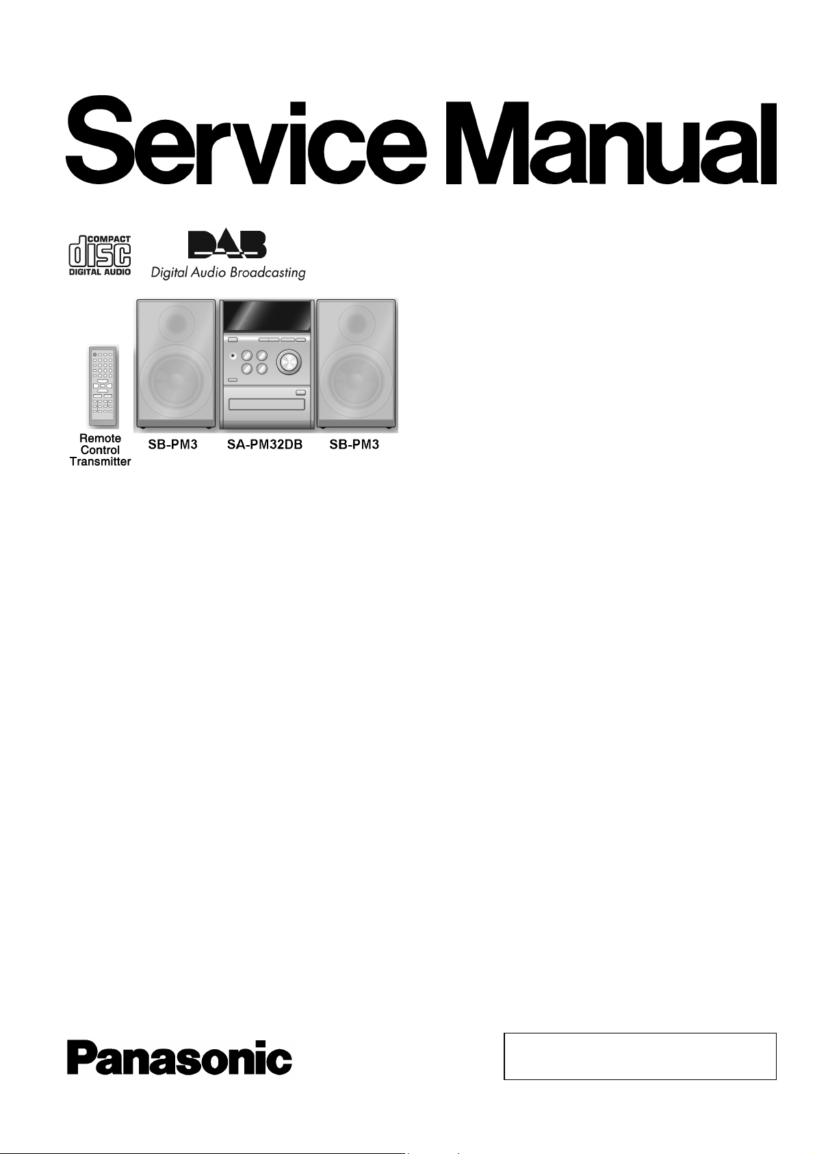
CD Stereo System
SA-PM32DBEB
Colour
(S)... Silver Type
ORDER NO. MD0603069C2
Specification
n Amplifier Section
RMS OUTPUT POWER both channel driven simultaneously
10% total harmonic distortion 5 W per channel (6 Ω)
Input impedance
MUSIC PORT 250 mV 12 kΩ
Output impedance
HEADPHONE 16 Ω to 32 Ω
Phone jack
Terminal Stereo, 3.5 mm
Music Port input jack
Terminal Stereo, 3.5 mm
DAB External antenna
Terminal F-Connector (75 Ω)
n FM Tuner Section
Frequency range 87.50 MHz to 108.00 MHz
(50 kHz step)
Sensitivity 3.2 µV (IHF)
S/N 26 dB 1.2 µV
ntenna terminals 75 Ω (unbalanced)
Preset station FM 15 stations
AM 15 stations
n AM Tuner Section
Frequency range 522 kHz to 1629 kHz
(9 kHz steps)
Sensitivity
S/N 20 dB (at 999 kHz) 1412 µV/m
n DAB Section
Frequency Band (Wavelength)
Band III (UK only) 11B ~ 12D (218.640 MHz ~
229.072 MHz)
Band III (Europe) 5A ~ 13F (174.928 MHz ~
239.200 MHz)
Intermediate frequency 1st : 38.912 MHz, 2nd : 2.048
MHz
Sensitivity *BER 4x10
MAX. Input Power 0dBm
Min Requirement -98 dBm
Selectivity
djacent Channel (Band III) 33 dB
Far-Off Channel (Band III) 45 dB
DAB memories 20 channels
n CD Section
Disc played [8 cm or 12 cm]
(1) CD-Audio (CD-DA)
(2) CD-R/RW (CD-DA, MP3 formatted disc)
(3) MP3
Sampling frequency
CD 44.1 kHz
-
© 2006 Matsushita Electric Industrial Co. Ltd.. All
rights reserved. Unauthorized copying and
distribution is a violation of law.
Page 2
A
SA-PM32DBEB
MP3 32 kHz, 44.1 kHz, 48 kHz
Bit rate
MP3 32 kbps to 384 kbps
Decoding 16/20/24 bit linear
Pickup
Beam source Semiconductor laser
Wavelength 785 nm
Laser power CLASS 1
udio output (Disc)
Number of channels 2 channel
Frequency response 20 Hz to 20 kHz (+1, -2dB)
Wow and flutter Below measurable limit
Digital filter 8fs
D/A converter MASH (1 bit DAC)
n General
Power supply AC 230 to 240 V, 50 Hz
Power consumption 25 W
Dimensions (W x H x D) 165 mm x 227 mm x 327 mm
Mass 2.8 kg
Operating temperature range +5°C to +35°C
Operation humidity range 5% to 90% RH (no condensation)
Power consumption in standby
mode
Notes :
1. Specifications are subject to change without notices. Mass and
dimensions are approximate.
2. Total harmonic distortion is measured by the digital spectrum
analyzer.
n System : SC-PM32DBEBS
Music center: SA-PM32DBEBS
Speaker: SB-PM3EG-M
0.8 W
CONTENTS
Page Page
1 Safety Precautions 4
1.1. General Guidelines
1.2. Caution for AC Cord
1.3. Before Repair and Adjustment
1.4. Protection Circuitry
2 Prevention of Electro Static Discharge (ESD) to
Electrostatically Sensitive (ES) Devices
3 Precaution of Laser Diode
4 Handling Precautions For Traverse Deck
5 Handling the Lead-free Solder
5.1. About lead free solder (PbF)
6 Accessories
7 Operating Instructions Procedures
7.1. Main Unit Operation
7.2. Remote Control Operation
7.3. Disc Information
8 Self diagnosis and special mode setting
8.1. Special Mode Table
8.2. Error Code Table
9 Assembling and Disassembling
9.1. Caution
9.2. Disassembly flow chart
9.3. Main Parts Location Diagram
9.4. Disassembly of Side Panel L & R
9.5. Disassembly of Top Cabinet Unit
9.6. Disassembly of Headphone P.C.B.
9.7. Disassembly of Front Panel
9.8. Disassembly of DAB Module unit
9.9. Disassembly of Panel P.C.B.
10
10
11
12
12
13
13
14
14
15
16
16
17
18
19
19
20
20
21
21
9.10. Disassembly of Rear Panel
4
5
6
6
7
8
9
9.11. Disassembly of Tuner Pack
9.12. Disassembly of Main P.C.B.
9.13. Disassembly of Power P.C.B.
9.14. Disassembly of Speaker Terminal P.C.B.
9.15. Disassembly of Transformer P.C.B.
9.16. Disassembly of CD Mechanism
9.17. Disassembly of Traverse Unit, Driving Gear, and Cam
Gear (CD Mechanism Unit)
9.18. Disassembly of Optical Pickup (CD Mechanism Unit)
9.19. Disassembly of Traverse Gear A and Traverse Gear B
(CD Mechanism Unit)
10 Service Fixture and Tools
11 Service Positions
11.1. Checking and Repairing Headphone P.C.B.
11.2. Checking and Repairing of DAB Module Unit and Panel
P.C.B.
11.3. Checking and Repairing of Transformer P.C.B.
11.4. Checking and Repairing of Main P.C.B.
11.5. Checking and Repairing of CD Servo P.C.B.
11.6. Checking and Repairing of Speaker Terminal P.C.B.
11.7. Checking and Repairing of Power P.C.B.
12 Voltage Measurement and Waveform Chart
12.1. Voltage Measurement
12.2. Waveform
13 Wiring Connection Diagram
14 Block Diagram
15 Notes of Schematic Diagram
16 Schematic Diagram
21
22
22
22
23
24
24
25
28
29
30
30
30
31
32
33
34
35
36
37
37
40
41
43
47
49
2
Page 3

SA-PM32DBEB
16.1. CD SERVO CIRCUIT 49
16.2. MAIN CIRCUIT and TUNER EXTENT CIRCUIT
16.3. PANEL CIRCUIT
16.4. POWER CIRCUIT
16.5. SPEAKER TERMINAL CIRCUIT, TRANSFORMER
CIRCUIT and HEADPHONE CIRCUIT
17 Printed Circuit Board
17.1. CD SERVO P.C.B
17.2. MAIN P.C.B and TUNER EXTENT P.C.B
17.3. PANEL P.C.B
17.4. POWER P.C.B and SPEAKER TERMINAL P.C.B
17.5. TRANSFORMER P.C.B and HEADPHONE P.C.B
18 Illustration of IC's, Transistors and Diodes
19 Terminal Function of IC's
50
52
53
19.1. IC7001 (MN6627954MA) IC SERVO
PROCESSOR/DIGITAL SIGNAL PROCESSOR/DIGITA L
FILTER D/A CONVERTER
19.2. IC7002 (BA5948FPE2) IC 4CH Drive
54
55
55
56
57
58
59
19.3. IC401 (C2CBYY000223) IC MICROPROCESSOR
20 Troubleshooting Flowchart (CD Section Circuit)
21 Exploded Views
21.1. Cabinet Parts Location
21.2. Traverse Deck Part Location
21.3. Packaging
22 Replacement Parts List
61
62
62
63
63
65
67
67
68
69
71
3
Page 4
SA-PM32DBEB
1 Safety Precautions
1.1. General Guidelines
1. When servicing, observe the original lead dress. If a short circuit is found, replace all parts which have been overheated or
damaged by the short circuit.
2. After servicing, ensure that all the protective devices such as insulation barriers, insulation papers shields are properly installed.
3. After servicing, check for leakage current checks to prevent from being exposed to shock hazards.
1.1.1. Leakage Current Cold Check
1. Unplug the AC cord and connect a jumper between the two prongs on the plug.
2. Using an ohmmeter measure the resistance value, between the jumpered AC plug and each expose d metallic cabine t part on
the equipment such as screwheads, connectors, control shafts, etc. When the exposed metallic part has a return path to the
chassis, the reading should be between 1MΩ and 5.2Ω.
When the exposed metal does not have a return path to the chassis, the reading must be
.
Figure 1
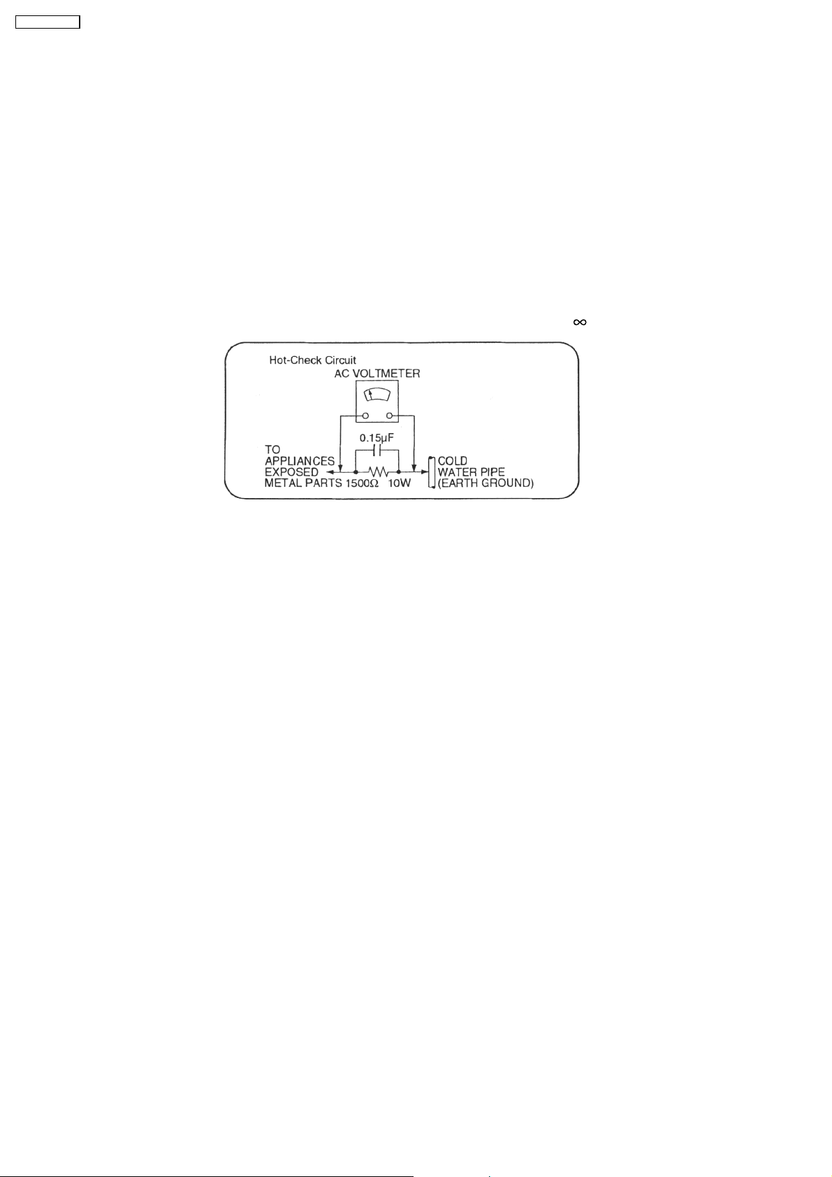
1.1.2. Leakage Current Hot Check (See Figure 1)
1. Plug the AC cord directly into the AC outlet. Do not use an isolation transformer for this check.
2. Connect a 1.5kΩ, 10 watts resistor, in parallel with a 0.15µF capacitors, between each exposed metallic part on the set and a
good earth ground such as a water pipe, as shown in Figure 1.
3. Use an AC voltmeter, with 1000 ohms/volt or more sensitivity, to measure the potential across the resistor.
4. Check each exposed metallic part, and measure the voltage at each point.
5. Reverse the AC plug in the AC outlet and repeat each of the above measurements.
6. The potential at any point should not exceed 0.75 volts RMS. A leakage current tester (Simpson Model 229 or equivalent) may
be used to make the hot checks, leakage current must not exceed 1/2 milliamp. should the measurement is outside of the limits
specified, there is a possibility of a shock hazard, and the equipment should be repaired and re-checked before it is returned
to the customer.
4
Page 5
1.2. Caution for AC Cord
SA-PM32DBEB
5
Page 6

SA-PM32DBEB
1.3. Before Repair and Adjustment
Disconnect AC power, discharge Power Supply Capacitors C501, C601, C807, C813, C814, C831, C839, C840, C909, C910,
C911, C923 & C966 through a 10Ω, 1W resistor to ground.
DO NOT SHORT-CIRCUIT DIRECTLY (with a screwdriver blade, for instance), as this may destroy solid state devices.
After repairs are completed, restore power gradually using a variac, to avoid overcurrent.
· Current consumption at AC 230-240 V, 50 Hz in NO SIGNAL mode at (volume minimal) should be ~160 mA.
1.4. Protection Circuitry
The protection circuitry may have operated if either of the following conditions are noticed:
· No sound is heard when the power is turned on.
· Sound stops during a performance.
The function of this circuitry is to prevent circuitry damage if, for example, the positive and negative speake r connection wires are
"shorted", or if speaker systems with an impedance less than the indicated rated impedance of the amplifier are used.
If this occurs, follow the procedure outlines below:
1. Turn off the power.
2. Determine the cause of the problem and correct it.
3. Turn on the power once again after one minute.
Note:
When the protection circuitry functions, the unit will not operate unless the power is first turned off and then on again.
6
Page 7
SA-PM32DBEB
2 Prevention of Electro Static Discharge (ESD) to
Electrostatically Sensitive (ES) Devices
Some semiconductor (solid state) devices can be damaged easily by electricity. Such components commonly are called
Electrostatically Sensitive (ES) Devices. Examples of typical ES devices are integrated circuits and some field-effect transistors and
semiconductor “chip” components. The following techniques should be used to help reduce the incidence of component damage
caused by electro static discharge (ESD).
1. Immediately before handlin g any semiconductor component or semiconductor-equiped assembly, drain off any ESD on your
body by touching a known earth ground. Alternatively, obtain and wear a commercially available discharging ESD wrist strap,
which should be removed for potential shock reasons prior to applyin g power to the unit under test.
2. After removing an electrical assembly equiped with ES devices, place the assembly on a conductive surface such as aluminium
foil, to prevent electrostatic charge build up or exposure of the assembly.
3. Use only a grounded-tip soldering iron to solder or unsolder ES devices.
4. Use only an anti-static solder remover device. Some solder removal devices not classified as “anti-static (ESD protected)” can
generate electrical charge to damage ES devices.
5. Do not use freon-propelled chemicals. These can generate electrical charges sufficient to damage ES devices.
6. Do not remove a replacement ES device from its protective package until immediately before you are ready to install it. (Most
replacement ES devices are packaged with leads electrically shorted together by conductive foam, aluminium foil or
comparable conductive material).
7. Immediately before removing the protective material from the leads of a replacement ES device, touch the protective material
to the chassis or circuit assembly into which the device will be installe d.
Caution
Be sure no power is applied to the chassis or circuit, and observe all other safety precautions.
8. Minimize body motions when handling unpackaged replacement ES devices. (Otherwise harmless motion such as the brushing
together of your clothes fabric or the lifting of your foot from a carpeted floor can generate static electricity (ESD) sufficient to
damage an ES device).
7
Page 8

SA-PM32DBEB
3 Precaution of Laser Diode
CAUTION:
This unit utilizes a class 1 laser.
Invisible laser radiation is emitted from the optical pickup lens.
When the unit is turned on:
1. Do not look directly into the pick up lens.
2. Do not use optical instruments to look at the pick up lens.
3. Do not adjust the preset variable resistor on the pickup lens.
4. Do not disassemble the optical pick up unit.
5. If the optical pick up is replaced, use the manufacturer’s specified replacement pick up only.
6. Use of control or adjustments or performance of procedures other than those specified herein may result in hazardous radiation
exposure.
CAUTION!
THIS PRODUCT UTILIZES A LASER.
USE OF CONTROLS OR ADJUSTMENTS OR PERFORMANCE OF PROCEDURES OTHER THAN THOSE SPECIFIED HEREIN MAY RESULT
IN HAZARDOUS RADIATION EXPOSURE.
8
Page 9
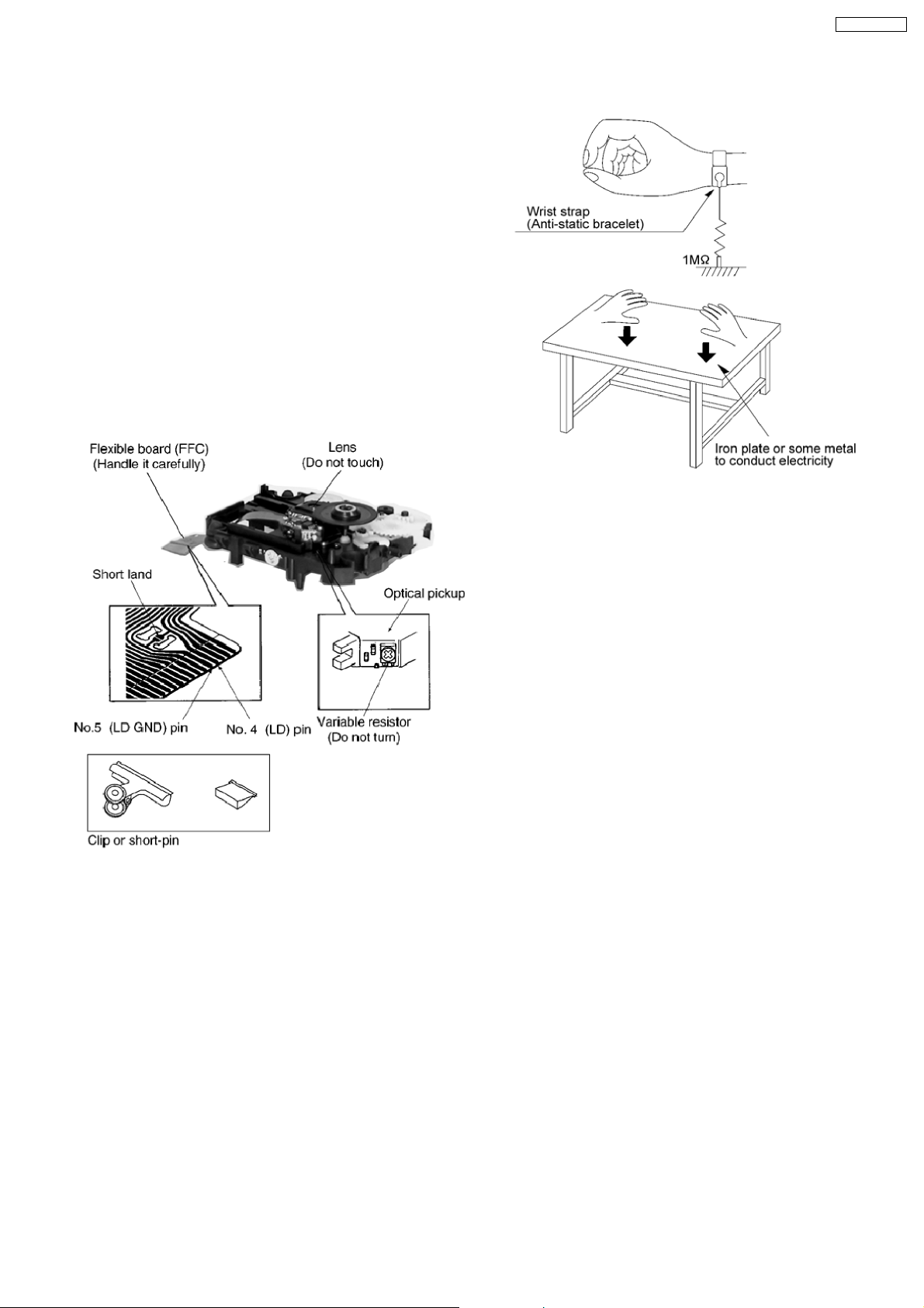
4 Handling Precautions For Traverse Deck
The laser diode in the traverse deck (optical pickup) may break
down due to potential difference caused by static electricity of
clothes or human body.
So, be careful of electrostatic breakdown during repair of the
traverse deck (optical pickup).
l Handling of CD traverse deck (optical pickup)
1. Do not subject the traverse deck (optical pickup) to
static electricity as it is extremely sensitive to electrical
shock.
2. The short land between the No.4 (LD) and No.5 (GND)
pins on the flexible board (FFC) is shorted with a solder
build-up to prevent damage to the laser diode.
3. Take care not to apply excessive stress to the flexible
board (FFC board) (Fig 4.1).
4. Do not turn the variable resistor (laser power
adjustment). It has already been adjusted.
SA-PM32DBEB
Fig 4.1
l Grounding for electrostatic breakdown prevention
1. Human body grounding (Fig 4.2)
Use the anti-static wrist strap to discharge the static
electricity from your body.
2. Work table grounding (Fig 4.2)
Put a conductive material (sheet) or steel sheet on the
area where the traverse deck (optical pickup) is placed,
and ground the sheet.
Caution :
The static electricity of your clothes will not be grounded
through the wrist strap. So, take care not to let your
clothes touch the traverse deck (optical pickup).
Fig 4.2
Caution when Replacing the Optical Pickup :
The traverse has a short point shorted with solder to protect
the laser diode against electrostatics breakdown. Be sure to
remove the solder from the short point before making
connections.
9
Page 10

SA-PM32DBEB
5 Handling the Lead-free Solder
5.1. About lead free solder (PbF)
Distinction of PbF P.C.B.:
P.C.B.s (manufactured) using lead free solder will have a PbF stamp on the P.C.B.
Caution:
· Pb free solder has a higher melting point than standard solder; Typically the melting point is 50 - 70°F (30 - 40°C) higher. Please
use a high temperature soldering iron. In case of soldering iron with temperature control, please set it to 700 ± 20°F (370 ±
10°C).
· Pb free solder will tend to splash when heated too high (about 1100°F/600°C).
· W hen soldering or unsoldering, please completely remove all of the solder on the pins or solder area, and be sure to heat the
soldering points with the Pb free solder until it melts enough.
10
Page 11
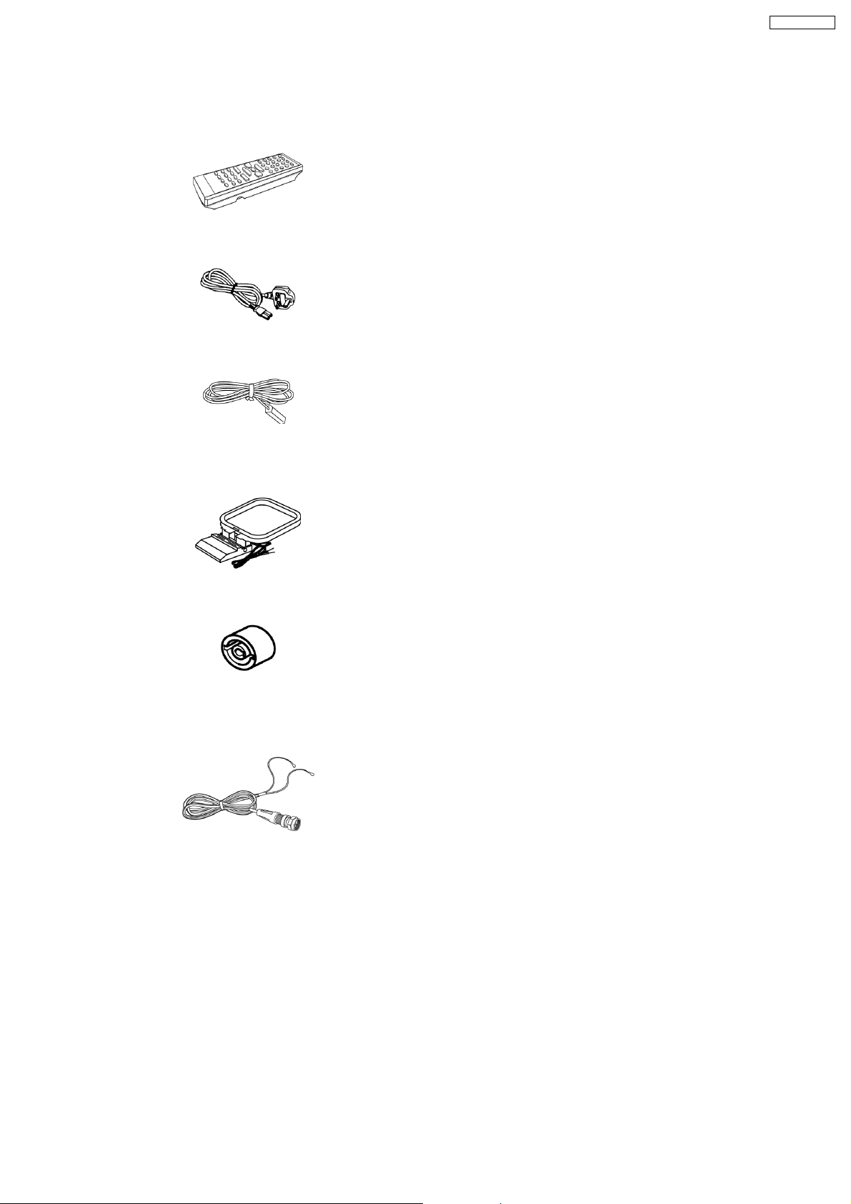
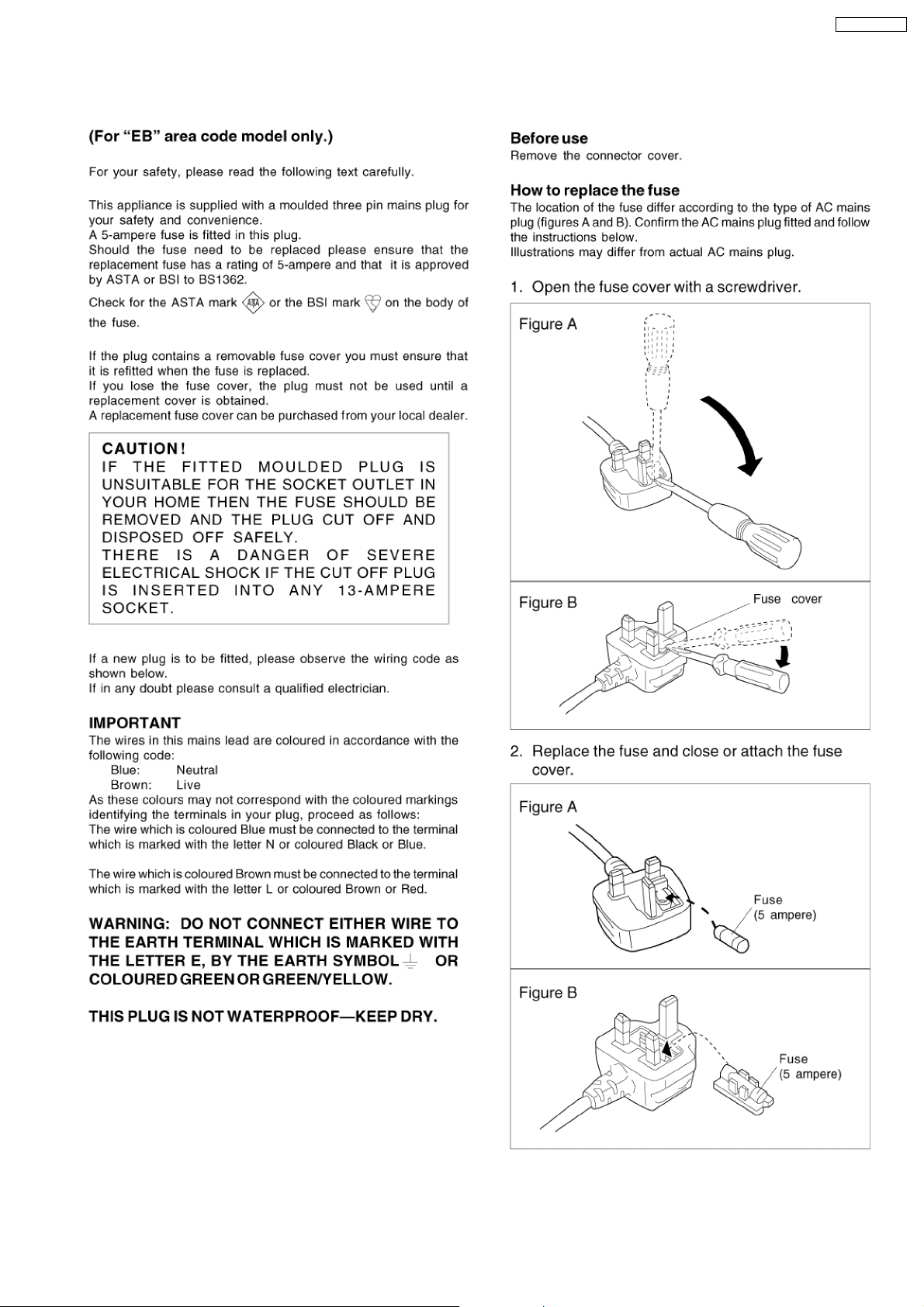
6 Accessories
Note : Refer to Packing Materials & Accessories (Section 22) for part number.
Remote control
AC cord
SA-PM32DBEB
FM indoor
antenna
AM loop antenna
Antenna
plug
adaptor
DAB antenna
11
Page 12
SA-PM32DBEB
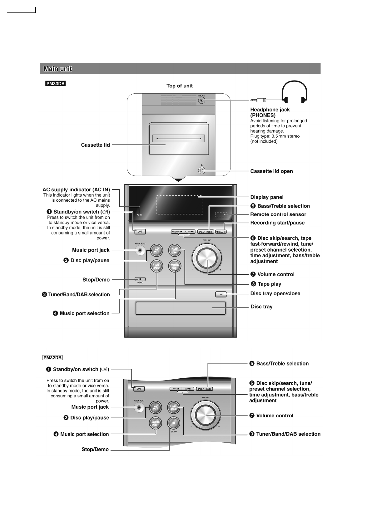
7 Operating Instructions Procedures
7.1. Main Unit Operation
12
Page 13

7.2. Remote Control Operation
SA-PM32DBEB
7.3. Disc Information
13
Page 14
SA-PM32DBEB
8 Self diagnosis and special mode setting
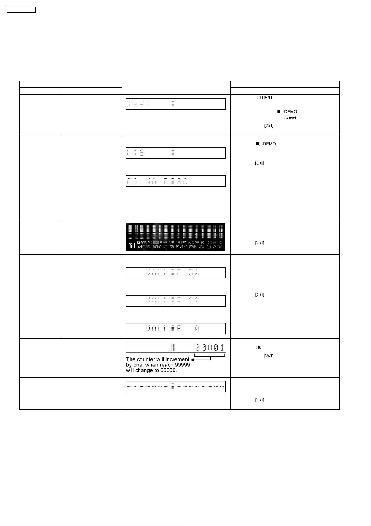
This unit is equipped with features of self-diagnostic & special mode setting for checking the functions & reliability.
8.1. Special Mode Table
Below is the various special modes for checking:-
Item FL Display Key Operation
Mode Name Description Front Key
Self -Diagnostic
Mode
Doctor Mode To enter into Doctor
FL Display Test To check the FL
Volume Setting To Forced Volume
To enter into self
diagnostic checking for
main unit.
Mode for checking of
various items and
displaying EEPROM and
firmware version.
(For more information,
refer to section 8.1.1)
Note: The microprocessor version as
shown is an example. It
will be revise when there
is an updates.
segments display (All
segments will light up)
Setting.
1.
2.
The Check Sum of EEPROM and firmware
version will be display for 1 sec.
* ROM correction
** Firmware version No:
1.
2.
1. Select [ ] for CD mode (Ensure no
tape or CD inserted).
2. Press and hold [
seconds follow by [
To exit, press
remote control.
In any mode:
1. Press [
by [4] and [7] on remote control.
To exit, press [ENTER] button on remote
control or
control.
In doctor mode:
1. Press [DIMMER] button on remote control.
To exit, press [ENTER] button on remote
control or
control.
In doctor mode:
1. Press [7] button on remote control.
2. Press [8] button on remote control.
3. Press [9] button on remote control.
To exit, press [ENTER] button on remote
control or
control.
button on main unit or
] button on main unit follow
button on main unit or remote
button on main unit or remote
button on main unit or remote
]button for 2
].
3.
Traverse Test To determine the
reliability of CD unit.
Cold Start To activate cold start ipon
next AC power up.
In doctor Mode:
1. Press [
To exit, press
remote control.
In doctor mode:
1. Press [SLEEP] button on remote control.
To exit, press [ENTER] button on remote
control or
control.
], [1], [2] button on remote control.
button on main unit or
button on main unit or remote
8.1.1. EEPROM Checksum (ROM correction)
Purpose : To check for micro-processor firmware version & EEPRO M check (ROM correction).
Below is the procedures for this mode.
Step 1: Enter into Doctor mode (For more information refer to section 8.1 on key operation to enter into this mode.
Step 2: Check for firmware version & EEPRO M checksum.
· W hen entering into DOCTOR MODE the firmware version & checksum of EEPROM (if applicable) will appear on FL display .
Below is information on the EEPROM IC (Rom correction) under 3 examples:
1. When EEPROM IC is detected and there is no ROM correction:
14
Page 15
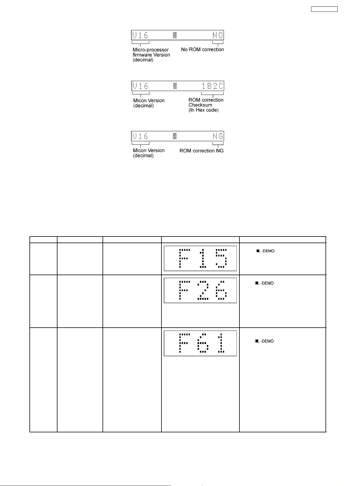
SA-PM32DBEB
2. When EEPROM IC is detected and has ROM correction:
3. When EEPROM IC is detected and has ROM correction but NG:
Note: Micro-processor firmware version refers to version No. (Eg.MS079_12) for micro-processor IC.
It is subject to change which would update accordingly.
· Rom correction checksum refers to the hex code that is display upon key buttons pressed if an EEPROM is loaded in the unit.
(Main P.C.B)
8.2. Error Code Table
Self-Diagnosis Function provides information on any problems occuring for the unit and its respective components by display ing
error codes. Thesed error code such as U**, H** and F** are stored in memory and held unless it is cleared.
The error code is automatically display after entering into self-diagnostic mode.
Error Code Diagnosis Contents Description of error Automatic FL Display Remarks
F15 CD REST SW
Abnormal
F26 Communication
between CD servo
LSI and micro-p
abnormal.
POWER
AMP output
abnormal
CD traverse position intial
setting operation failsafe
counter (1000 ms) waiting
for REST SW toturn on.
Error No. shall be clear by
force or during cold start.
CD function DTMS
command, after system
setting, If SENSE = ´L´
cannot be detected.
Memory shall contain F26
code. After Power on, CD
function shall continue,
error display shall be "NO
DISC". Error No. shall be
clear by force or cold start.
During normal operation, if
DCDET becomes "L",
normal POWER OFF
process shall not be
executed, PCONT shall be
switched to "L"
immediately. "GOODBYE"
shall not be display but the
error display F61 is
displayed instead. 2
seconds after the F61
displayed, ECONO shall be
set to "L" and FL display
shall be turned off. The
error content shall be
memorized when the
abnormality occurs and can
be display in the C-mecha
self-diagnostic mode
described later.
For CD unit (For Traverse).
Press [
error.
For CD unit (For Traverse).
Press [
error.
For Power Supply Related Error
Detection.
Press [
error.
] on main unit for next
] on main unit for next
] on main unit for next
15
Page 16

SA-PM32DBEB
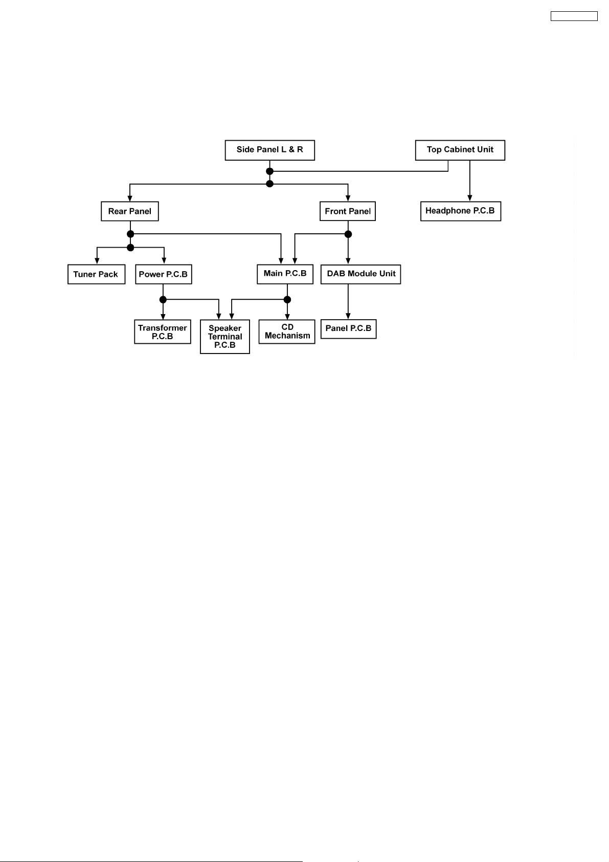
9 Assembling and Disassembling
9.1. Caution
“ATTENTION SERVICER”
Some chassis components may be have sharp edges. Be careful when disassembling and servicing.
1. This section describes procedures for checking the operation of the major printed circuit boards and replacing the main
components.
2. For reassembly after operation checks or replacement, reverse the respective procedures.
Special reassembly procedures are described only when required.
3. Select items from the following index when checks or replacement are required.
Warning:
This product uses a laser diode. Refer to “Precaution of Laser Diode”.
Below is the list of disassembly sections
· Disasse mbly of Side Panel L & R
· Disasse mbly of Top Cabinet Unit
· Disasse mbly of Headphone P.C.B.
· Disasse mbly of Front Panel
· Disasse mbly of DAB Module Unit
· Disasse mbly of Panel P.C.B.
· Disasse mbly of Rear Panel
· Disasse mbly of Tuner Pack
· Disasse mbly of Main P.C.B.
· Disasse mbly of Power P.C.B.
· Disasse mbly of Speaker Terminal P.C.B.
· Disasse mbly of Transformer P.C.B.
· Disasse mbly of CD Mechanism
· Disasse mbly of Traverse Unit, Driving Gear, and Cam Gear (CD Mechanism Unit)
· Disasse mbly of Optical Pickup (CD Mechanism Unit)
· Disasse mbly of Traverse Gear A and Traverse Gear B (CD Mechanism Unit)
16
Page 17
SA-PM32DBEB
9.2. Disassembly flow chart
The following chart is the procedure for disassembling the casing and inside parts for internal inspection when carrying out the
servicing.
To assemble the unit, reverse the steps shown in the chart below.
17
Page 18

SA-PM32DBEB
9.3. Main Parts Location Diagram
18
Page 19
SA-PM32DBEB
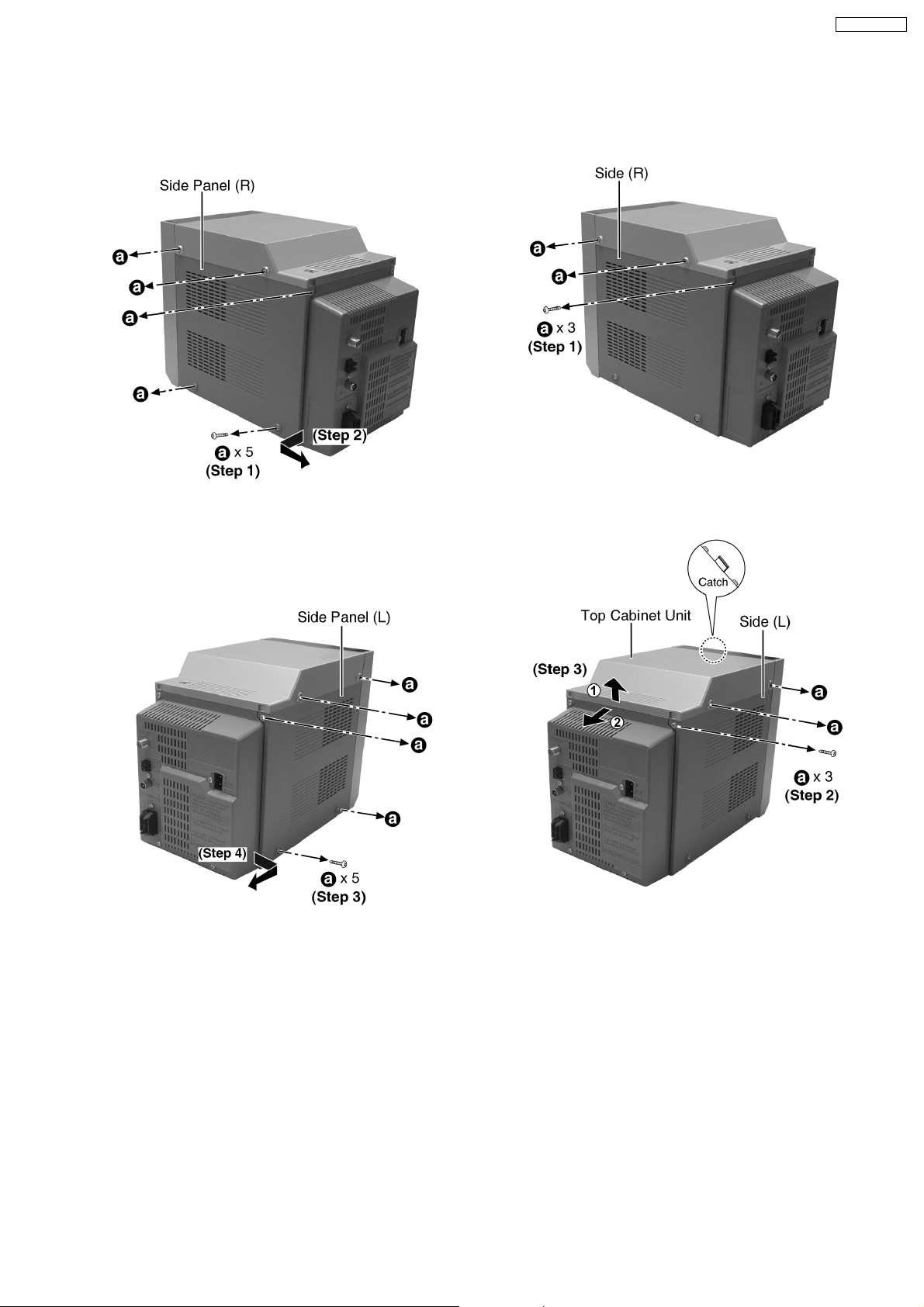
9.4. Disassembly of Side Panel L &
R
· Disasse mbly of Side Panel (R)
Step 1: Remove 5 screws.
Step 2: Remove the side panel (R) as arrow shown.
9.5. Disassembly of Top Cabinet
Unit
Step 1: Remove 3 screws.
· Disasse mbly of Side Panel (L)
Step 3: Remove 5 screws.
Step 4: Remove the side panel (L) as arrow shown.
Step 2: Remove 3 screws.
Step 3: Lift up the top cabinet unit, push backward
as arrow shown and flip top cabinet unit sideway.
(Be careful of the catch)
19
Page 20
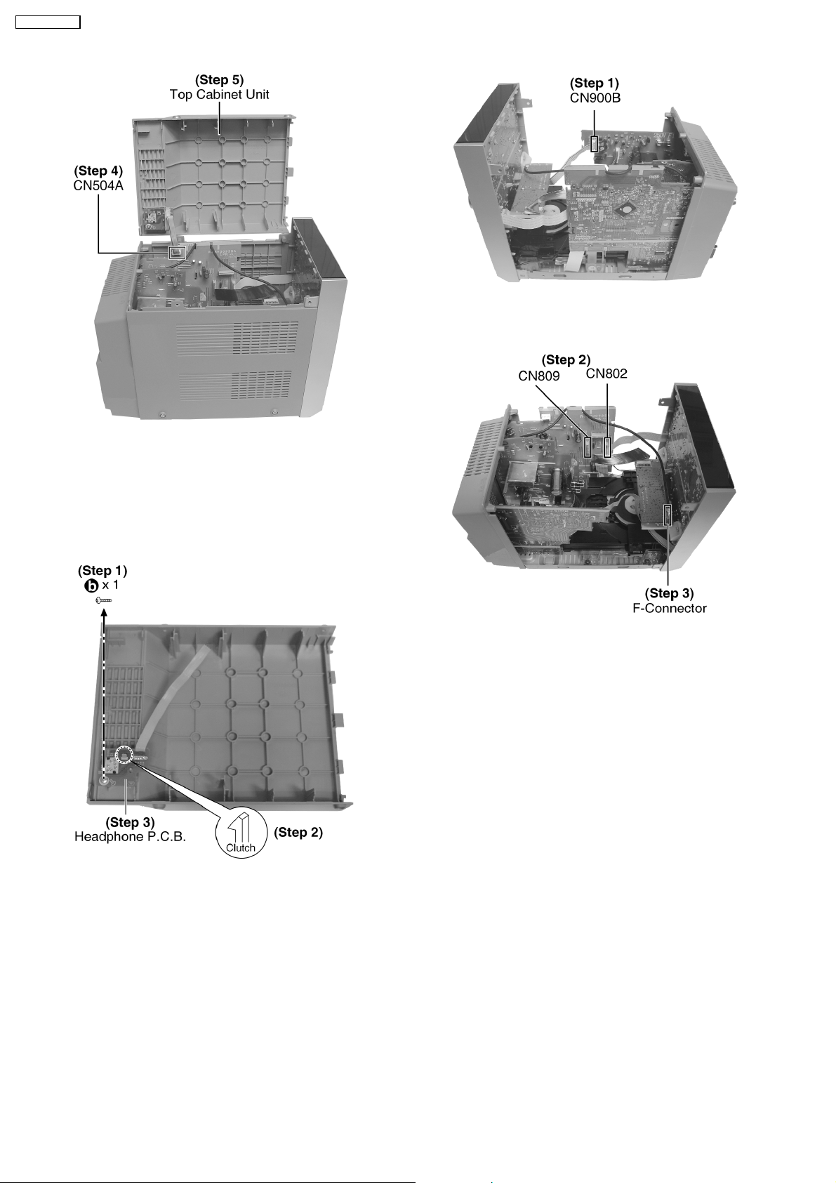
SA-PM32DBEB
Step 1: Detach connector (CN900B).
Step 4: Detach connector (CN504A).
Step 5: Remove top cabinet unit.
9.6. Disassembly of Headphone
P.C.B.
· Follow the (Step 1) - (Step 5) of Item 9.5.
Step 2: Disconnect FFC cable (CN802 and CN809).
Step 3: Disconnect F-Connector.
Step 1: Remove 1 screw.
Step 2: Release the clutch.
Step 3: Remove the Headphone P.C.B.
9.7. Disassembly of Front Panel
· Follow the (Step 1) - (Step 4) of Item 9.4.
· Follow the (Step 3) - (Step 5) of Item 9.5.
20
Page 21

Step 1: Remove 2 screws.
Step 2: Remove the DAB Module Unit
SA-PM32DBEB
Step 4: Release 3 claws.
Step 5: Remove the Front Panel as arrow shown.
9.8. Disassembly of DAB Module
unit
· Follow the (Step 1) - (Step 4) of Item 9.4.
· Follow the (Step 3) - (Step 5) of Item 9.5.
· Follow the (Step 1) - (Step 5) of Item 9.7.
9.9. Disassembly of Panel P.C.B.
· Follow the (Step 1) - (Step 4) of Item 9.4.
· Follow the (Step 3) - (Step 5) of Item 9.5.
· Follow the (Step 1) - (Step 5) of Item 9.7.
· Follow the (Step 1) - (Step 2) of Item 9.8.
Step 1: Remove 8 screws.
Step 2: Remove the Volume Knob.
Step 3: Release 2 catches.
Step 4: Remove the Panel P.C.B.
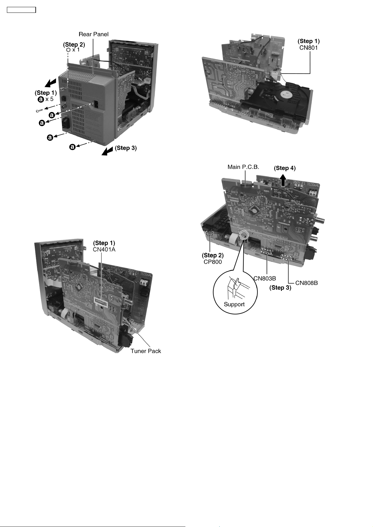
9.10. Disassembly of Rear Panel
· Follow the (Step 1) - (Step 4) of Item 9.4.
· Follow the (Step 3) - (Step 5) of Item 9.5.
21
Page 22
SA-PM32DBEB
Step 1: Detach the FFC CN801.
Step 1: Remove 5 screws.
Step 2: Remove 1 nut.
Step 3: Remove the Rear Panel as arrow shown.
9.11. Disassembly of Tuner Pack
· Follow the (Step 1) - (Step 4) of Item 9.4.
· Follow the (Step 3) - (Step 5) of Item 9.5.
· Follow the (Step 1) - (Step 3) of Item 9.10.
Step 1: Detach the connec tor CN401A and remove
the tuner pack as arrow shown.
9.12. Disassembly of Main P.C.B.
· Follow the (Step 1) - (Step 4) of Item 9.4.
· Follow the (Step 3) - (Step 5) of Item 9.5.
· Follow the (Step 1) - (step 5) of Item 9.7.
· Follow the (Step 1) - (step 3) of Item 9.10.
Step 2: Detach connector CP800.
Step 3: Detach connector CN803B and CN808B.
Step 4: Remove the Main P.C.B. as arrow shown.
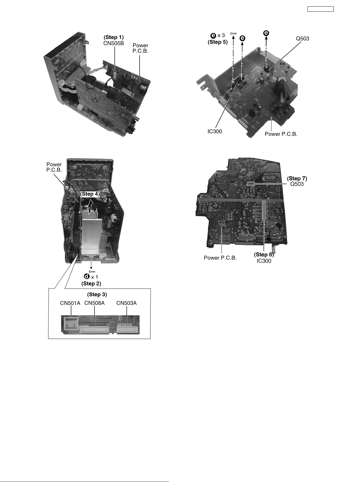
9.13. Disassembly of Power P.C.B.
· Follow the (Step 1) - (Step 4) of Item 9.4.
· Follow the (Step 3) - (Step 5) of Item 9.5.
· Follow the (Step 1) - (Step 3) of Item 9.10.
22
Page 23
SA-PM32DBEB
Step 1: Detach the connector CN505B.
Step 5: Remove 3 screws.
Step 6: Unsolder the terminal of Power Amp IC
(IC300) and replace the component.
Step 7: Unsolder the terminal of Transistor (Q503)
and replace the component.
9.14. Disassembly of Speaker
Terminal P.C.B.
Step 2: Remove 1 screw.
Step 3: Detach the connector CN501A, CN508A
and CN503A.
Step 4: Remove the Power P.C.B. as arrow shown.
· Replacement of Power Amplifier IC
· Follow the (Step 1) - (Step 4) of Item 9.4.
· Follow the (Step 3) - (Step 5) of Item 9.5.
· Follow the (Step 1) - (step 3) of Item 9.10.
· Follow the (Step 3) of Item 9.12.
· Follow the (Step 1) - (step 4) of Item 9.13.
23
Page 24

SA-PM32DBEB
Step 1: Remove 1 screw.
Step 2: Release the clutch.
Step 3: Remove the Speaker Terminal P.C.B. as
arrow shown.
9.15. Disassembly of Transformer
P.C.B.
· Follow the (Step 1) - (Step 4) of Item 9.4.
· Follow the (Step 3) - (Step 5) of Item 9.5.
· Follow the (Step 1) - (Step 3) of Item 9.10.
· Follow the (Step 1) - (Step 4) of Item 9.13.
Step 1: Detach the connector CN900B.
Step 2: Remove 4 screws.
Step 3: Remove the Transformer P.C.B. as arrow
shown.
9.16. Disassembly of CD
Mechanism
· Follow the (Step 1) - (Step 4) of Item 9.4.
· Follow the (Step 3) - (step 5) of Item 9.5.
· Follow the (Step 1) - (step 5) of Item 9.7.
· Follow the (Step 1) - (step 3) of Item 9.10.
· Follow the (Step 1) - (step 4) of Item 9.12.
24
Page 25

Step 1: Remove 4 screws.
Step 2: Remove the Main P.C.B. support.
Step 3: Remove CD Mechanism as arrow shown.
SA-PM32DBEB
9.17. Disassembly of Traverse Unit,
Driving Gear, and Cam Gear
(CD Mechanism Unit)
9.17.1. Disassembly of the Traverse Unit
· Follow the (Step 1) - (Step 4) of Item 9.4.
· Follow the (Step 3) - (Step 5) of Item 9.5.
· Follow the (Step 1) - (Step 5) of Item 9.7.
· Follow the (Step 1) - (Step 3) of Item 9.10 .
· Follow the (Step 1) - (Step 4) of Item 9.12.
· Follow the (Step 1) - (Step 3) of Item 9.16.
· Disasse mbly of gears drive
25
Page 26

SA-PM32DBEB
26
Page 27

SA-PM32DBEB
27
Page 28

SA-PM32DBEB
9.18. Disassembly of Optical Pickup
(CD Mechanism Unit)
· Follow the (Step 1) - (Step 4) of Item 9.4.
· Follow the (Step 3) - (Step 5) of Item 9.5.
· Follow the (Step 1) - (Step 5) of Item 9.7.
· Follow the (Step 1) - (Step 3) of Item 9.10 .
· Follow the (Step 1) - (Step 4) of Item 9.12.
· Follow the (Step 1) - (Step 3) of Item 9.16.
· Follow the (Step 1) - (Step 4) of Item 9.19.1.
28
Page 29

· Follow the (Step 1) - (Step 3) of Item 9.10 .
· Follow the (Step 1) - (Step 4) of Item 9.12.
· Follow the (Step 1) - (Step 3) of Item 9.16.
· Follow the (Step 1) - (Step 2) of Item 9.19.1.
SA-PM32DBEB
9.19. Disassembly of Traverse Gear
A and Traverse Gear B (CD
Mechanism Unit)
· Follow the (Step 1) - (Step 4) of Item 9.4.
· Follow the (Step 3) - (Step 5) of Item 9.5.
· Follow the (Step 1) - (Step 5) of Item 9.7.
29
Page 30

SA-PM32DBEB
10 Service Fixture and Tools
Service Tools
Extension P.C.B.
(A) Main P.C.B. - Speaker Terminal P.C.B. RFKZPM33E
11 Service Positions
Note: For description of the disassembly procedures, see the Section 9
11.1. Checking and Repairing Headphone P.C.B.
30
Page 31

11.2. Checking and Repairing of DAB Module Unit and Panel P.C.B.
SA-PM32DBEB
31
Page 32

SA-PM32DBEB
11.3. Checking and Repairing of Transformer P.C.B.
32
Page 33

11.4. Checking and Repairing of Main P.C.B.
SA-PM32DBEB
33
Page 34

SA-PM32DBEB
11.5. Checking and Repairing of CD Servo P.C.B.
34
Page 35

11.6. Checking and Repairing of Speaker Terminal P.C.B.
SA-PM32DBEB
35
Page 36

SA-PM32DBEB
11.7. Checking and Repairing of Power P.C.B.
36
Page 37

12 Voltage Measurement and Waveform Chart
Note:
· Indicated voltage values are the standard values for the unit measured by the DC electronic circuit tester (high-impedance)
with the chassis taken as standard.
Therefore, there may exist some errors in the voltage values, depending on the internal impedance of the DC circuit tester.
· Circuit voltage and waveform described herein shall be regarded as reference information when probing defect point
because it may differ from actual measuring value due to difference of Measuring instrument and its measuring condition
and product itself.
12.1. Voltage Measurement
12.1.1. CD SERVO P.C.B
SA-PM32DBEB
Ref No.
MODE 1 234567891011121314151617181920
CD PLAY 0 00 0000000000000001.33.3
STANDBY 00 0 0000000000000.20.2000.3
Ref No.
MODE 21 22 23 24 25 26 27 28 29 30 31 32 33 34 35 36 37 38 39 40
CD PLAY 1.6 0 1.6 0 1.8 0 3.3 1.5 3.3 3.3 0 0 1.6 1.6 1.6 2 2 1.4 1.8 1.8
STANDBY 0 0 0 0 0 0 0.4 0 0.2 0.2 0 0 0.2 0 0 0 0.2 0.2 0.2 0.2
Ref No.
MODE 41 42 43 44 45 46 47 48 49 50 51 52 53 54 55 56 57 58 59 60
CD PLAY 0.2 2.4 0 1.8 1.2 1.8 3.3 1.2 1.2 1.2 1.7 1.9 0.8 1.5 1.4 0 0 3 1.5 0
STANDBY 0 0.3 0 0 0.2 0.1 0.3 0.4 0.2 0.2 0.1 0.1 0.3 0 0 0 0 0.4 0 0
Ref No.
MODE 61 62 63 64 65 66 67 68 69 70 71 72 73 74 75 76 77 78 79 80
CD PLAY 3.3 0 0 0 0 0 3.1 3.1 3.1 2.5 0 3.1 0 1.6 0 1.5 3.3 0 3.3 1.6
STANDBY 0.2 0.2 0.2 0.2 0.2 0.2 0 0 0 0 0 0 0.2 0.3 0.3 0 0.2 0 0.2 0.1
Ref No.
MODE 81 82 83 84 85 86 87 88 89 90 91 92 93 94 95 96 97 98 99 100
CD PLAY 1.62.300000000 0 03.30000000
STANDBY 0.10.200000000 0 00.3000000 0
Ref No.
MODE 1 234567891011121314151617181920
CD PLAY 1.601.60000007.54.23.53.53.503.303.87.50
STANDBY 00 0 00000000000000000
Ref No.
MODE 21 22 23 24 25 26 27 28
CD PLAY 0 7.5 0 0 7.5 0 1.6 0
STANDBY 00 0 00000
Ref No.
MODE E C B
CD PLAY 3.3 2.4 2.4
STANDBY 0.3 0 0.3
Q7601
IC7001
IC7001
IC7001
IC7001
IC7001
IC7002
IC7002
CD SERVO P.C.B
37
Page 38

SA-PM32DBEB
12.1.2. MAIN P.C.B
Ref No.
MODE 1 234567891011121314151617181920
CD PLAY 0 0 0 0 0 0 3.1 0 0 1.3 0.7 3.1 1.5 0 1.4 3.1 3.1 3.1 0 1.8
STANDBY 0 0 0 0 0 0 3.1 0 0 0.4 0.7 3.1 1.5 0 1.4 0 3.1 3.1 0 1.8
Ref No.
MODE 21 22 23 24 25 26 27 28 29 30 31 32 33 34 35 36 37 38 39 40
CD PLAY 3.100000.83.12.200.5000000002.92
STANDBY 0 0 0 00000000000000000
Ref No.
MODE 41 42 43 44 45 46 47 48 49 50 51 52 53 54 55 56 57 58 59 60
CD PLAY 0 0 3.1 0 0 0 0 1.8 3.1 0 0.1 1.3 0 0 0 1.4 3.1 0 0 0
STANDBY 0 0 0 0000000 02.10 000.10000
Ref No.
MODE 61 62 63 64 65 66 67 68 69 70 71 72 73 74 75 76 77 78 79 80
CD PLAY 1.43.10000003.13.103.100000003.1
STANDBY 0.13.10000000000000000.100
Ref No.
MODE 81 82 83 84 85 86 87 88 89 90 91 92 93 94 95 96 97 98 99 100
CD PLAY 0 0 0 0 1.4 0 0 0 3.1 0 0 3.1 3.1 3.1 0 0 3.1 3.1 3.1 1.5
STANDBY 00.10.100000003.13.13.13.12.503.13.13.11.6
Ref No.
MODE 1 2345678
CD PLAY 4.8 4.8 4.6 0 4.5 4.8 4.8 9
STANDBY 0 0 0 00000
Ref No.
MODE 1 234567891011121314151617181920
CD PLAY 4.5 4.5 4.5 4.5 4.5 4.5 4.5 4.5 4.5 4.5 4.5 4.5 4.5 4.5 4.5 0 0 0 8.8 8.8
STANDBY 0.4 0.4 0.3 0 0.3 0.3 0.3 0.3 0.3 0.3 0.3 0.3 0.3 0.3 0 0 0 0 0.3 0.3
Ref No.
MODE 21 22 23 24 25 26 27 28 29 30 31 32
CD PLAY 4.5 4.5 4.5 4.5 4.5 4.5 4.5 4.5 4.5 4.5 4.5 4.5
STANDBY 0.3 0.3 0.3 0.3 0.3 0.3 0.3 0.3 0.3 0.3 0.3 0.3
Ref No.
MODE 1 2 3
CD PLAY 5.7 0 3.9
STANDBY 5.8 0 3.9
Ref No.
MODE 1 2345
CD PLAY 0 0 4.8 0 3.3
STANDBY 0 0 0 0 0.2
Ref No.
MODE 1 2345678
CD PLAY 03.10 00000
STANDBY 03.10 00000
Ref No.
MODE E C B E C B E C B E C B E C B
CD PLAY 0 0 0.3 0 0 0.3 0 0 0.3 0 0 0.3 9.6 0.3 9.7
STANDBY 0 0 0 000 00 0 000 000
Ref No.
MODE E C B E C B E C B E C B E C B
CD PLAY 0 9.7 0 0 3.1 0 0 4.8 0 4.8 0 4.8 0 0 3.1
STANDBY 0 00 03.10 000 000 000
Ref No.
MODE E C B E C B
CD PLAY 0 2.1 0 0 2.1 0
STANDBY 0 0 0 0 0 0
MAIN P.C.B
IC401
IC401
IC401
IC401
IC401
IC700
IC800
IC800
IC801
IC802
IC804
Q221 Q222 Q421 Q422 Q750
Q751 Q800 Q801 Q802
Q807 Q808
Q803
38
Page 39

12.1.3. PANEL P.C.B
Ref No.
MODE 1 2345
CD PLAY 4.8 0 4.8 0 3.3
STANDBY 0.1 0 0.1 0 0.2
12.1.4. POWER P.C.B
Ref No.
MODE 1 23456789101112
CD PLAY 12.45.703.830004.25.705.7
STANDBY 00.200.2000000.200.2
Ref No.
MODE E C B E C B E C B E C B E C B
CD PLAY 12.4 11.4 12.4 4.6 11.6 5.6 12.3 9.7 11.6 5 9.1 5.6 4.8 7.5 5.5
STANDBY 2.8 2.4 2.8 2.4 2.5 3.2 2.9 0.2 2.5 2.4 0 0 0 0 0
Ref No.
MODE E C B E C B
CD PLAY 7.5 9.7 8.2 8.8 9.1 9.5
STANDBY 0 0.1 0.1 0 0 0
Q500 Q501 Q503 Q504
Q507 Q530
SA-PM32DBEB
PANEL P.C.B
IC900
POWER P.C.B
IC300
Q505
12.1.5. TRANSFORMER P.C.B
Ref No.
MODE E C B E C B E C B E C B
CD PLAY 0 0.2 0.8 5.7 13.8 6.4 0 1.7 2.8 31.2 32.2 31.8
STANDBY 0 5.7 0 5.7 13.8 6.4 0 1.7 2.6 0 0.4 0.4
Q600 Q601 Q602 Q603
TRANSFORMER P.C.B
39
Page 40

SA-PM32DBEB
12.2. Waveform
CN801 PIN 7
CD PLAY
3.52Vp-p (25msec.div)
CN802 PIN 15
CD PLAY
3.28Vp-p (10msec.div)
IC401 PIN 19
CD PLAY
3.36Vp-p (10msec.div)
CN801 PIN 8
CD PLAY
3.4Vp-p (10msec.div)
CN803B PIN 5
CD PLAY
3.2Vp-p (10msec.div)
IC401 PIN 26
CD PLAY
3.24Vp-p (10msec.div)
CN801 PIN 15
CD PLAY
448mVp-p (1msec.div)
IC401 PIN 13
CD PLAY
3.52Vp-p (50nsec.div)
IC401 PIN 28
CD PLAY
3.44Vp-p (5usec.div)
CN801 PIN 17
CD PLAY
364mVp-p (1msec.div)
IC401 PIN 15
CD PLAY
2.28Vp-p (100nsec.div)
IC401 PIN 30
CD PLAY
3.48Vp-p (10msec.div)
IC401 PIN 39
CD PLAY
3.84Vp-p (10msec.div)
IC401 PIN 42
CD PLAY
3.4Vp-p (25msec.div)
IC401 PIN 43
CD PLAY
3.52Vp-p (10msec.div)
40
IC401 PIN 48
CD PLAY
3.6Vp-p (25msec.div)
Page 41

13 Wiring Connection Diagram
SA-PM32DBEB
H
HEADPHONE P.C.B.
SOLDER SIDE
AC IN
230V-240V
50Hz
JK600
SOLDER SIDE
CAUTION
RISK OF ELECTRIC SHOCK
AC VOLTAGE LINE.
PLEASE DO NOT TOUCH THIS P.C.B
G
TRANSFORMER P.C.B.
T600
(Back Up Transformer)
T601
(Power Transformer)
PbF
CN505B
SOLDER SIDE
CN900B
5
.
.
.
1
.
.
.
.
.
.
.
.
8
1
CN802
15
.
14
.
.
.
.
.
.
.
.
.
.
.
.
.
2
1
2 1
CN801
2 . . . . . . . . 16
1 . . . . . . . . . . 17
CP800
CN809
18
.
17
.
.
.
.
.
.
.
.
.
.
.
.
.
.
.
.
1
DAB MODULE UNIT
.
.
.
2
CD OPEN SW
1..4
CN504A
B
MAIN P.C.B.
To DAB Module unit
CN401A
1 . . . . . . . . . . 10
CN505B
1
.
.
.
.
3
JK809
DAB ANT
JK900
PbF
HEADPHONE
4 . . 1
WH504
Tuner Pack
1 . . . . . . . . . . 10
CN10
Z401
1 . . . . . . . . . . 10
CN803B
9 . . . . . . . . . . . 1
CN808B
13 . . . . . . . . . . . . . . . . 1
PbF
SOLDER SIDE
PbF
C
TUNER EXTENT P.C.B.
SENSOR
VOLUME
Z901
CN901A
15
.
14
.
.
.
.
.
.
.
.
.
.
.
.
2
1
SOLDER SIDE
VR900
FL900
D
PANEL P.C.B.
PbF
JK303
SOLDER SIDE
WH505A
1
.
.
.
.
.
.
.
.
MUSIC
PORT
8
E
POWER P.C.B.
CN501B
4 . . 1
CN503B
9 . . . . . . . . . 1
W
H
9
0
0
5
.
.
.
1
CN508B
13 . . . . . . . . . . . . . . 1
PbF
CN7002
17
.
16
.
.
.
.
.
.
.
.
.
.
.
2
1
A
CD SERVO P.C.B.
SOLDER SIDE
CN
.
.
.
.
.
.
.
15
16
OPTICAL PICKUP
7001
1
.
2
.
.
.
.
.
.
.
.
.
.
.
.
.
.
PbF
9 . . . . . . . . . 1
CN803A
F
SPEAKER TERMINAL P.C.B.
CN503A
9 . . . . . . . . . 1
CN508A
13 . . . . . . . . . . . . . . 1
13 . . . . . . . . . . . . . . 1
CN808A
CN501A
4 . . 1
0
K
5
J
SOLDER SIDE
PbF
1
SPEAKERS
41
Page 42

SA-PM32DBEB
42
Page 43

14 Block Diagram
OPTICAL PICKUP
SA-PM32DBEB
PHOTO DETECTOR
EE EE
D C
A B
D C
EFEF
SEMICONDUCTOR
LASER
B
FOCUS
COIL
TRACKING
COIL
35
E
40
A
39
C
38
B
37
D
36
Q7601
SWITCH
LD_SW
F
41
PD
42
LD
OUTL
OUTR
56
59
CD SIGNAL
RCH
TO MAIN BLOCK
A
IC7002
BA5948FPE2
4CH DRIVE
26
VREF
F+
F-
T+
T-
D3-
15
[CH3]
D3+
16
D4-
17
[CH4]
18
D4+
LEVEL
SHIFT
LEVEL
SHIFT
IN3
28
27
IN4
B
FOP
TRP
BLKCK
TX
NRST
MLD
MCLK
MDATA
STAT
71
BLKCK
66
TX
72
NRST
69
MLD
67
MCLK
68
MDATA
70
STAT
IC7001
MN6627954MA
LSI IC
SPOUT
TRVP
TRP
FOP
21
22
PC
23
24
25
SPOUT
PC
TRVP
TRP
FOP
M7301
TRAVERSE
MOTOR
M7302
SPINDLE
MOTOR
D2+14
M
M
[CH2]
13
D2-
D1+
12
[CH1]
D1-
11
LEVEL
SHIFT
LEVEL
SHIFT
MUTE
[CH1]
MUTE
[CH2]
IN2
1
3
IN1
PC1
4
PC2
2
TRVP
LOADING
SPOUT
X1
X2
81 80
X7201
PC
S7201
RESET SWITCH
RESTSW
43
Page 44

SA-PM32DBEB
JK303
AUX INPUT JACK
IC800
A1(A2)
5(6)
LEFT(RIGHT)18S1
C1(C2)
22(21)
9(10)
C1BB00000732
ASP
SC
17
IC700
C0ABBB000297
FILTER
FILTER
OP AMP
Q221,Q222
(Q421,Q422)
MUTING
SWITCH
D1(D2)
B1(B2)
11(12)
7(8)
CD SIGNAL
DAB SIGNAL
HEADPHONE
RCH
JK900
TO
DAB MODULE
DAB SIGNAL
DAB_LCH
(DAB_RCH)
D
VOL_JOG
95
VR900
VOLUME JOG
E_DATA
24
5
6
D0
D1
IC804
EEPROM
( NOT SUPPLIED )
D_NRST
Z401
TUNER PACK
71ST71
IC401
C2CBYY000223
MICROPROCESSOR
E_CLK
E_CS
23
22
4
E_CLK
3
E_CS
S900~S910
KEY194KEY2
93
KEY SW
TUNED
70CL69
SDA
27
FL DISPLAY
26
/FL_RESET
B
FL900
FL_CS
30
FL_DATA
D906
STANDBY LED
FROM
TRANSFORMER
28
FL_CLK
67
68
ASP_DATA
ASP_CLK
XCIN10XCOUT
11
X801
32.678KHz
1,3,5
IC900
C0DBZGC00067
3.3V REGULATOR
2
XOUT
XIN
15
13
X800
10MHz
IC401
C2CBYY000223
MICROPROCESSOR
B
D_DOWFIC
D_MPUMOD
52
53
54
D_DOWFIC
D_MPUMOD
RMT
18
Z901
REMOTE SENSOR
51
D_NRST
D_LOCKDET
D_NRFRESET
50
D_LOCKDET
B
D_PLLSDA
45
D_PLLSDA
D_NRFRESET
/RESET
12
Q800
RESET
SWITCH
D_PLLSCL
44
DMPU_CLK
37
D_PLLSCL
DMPU_TX
36
DMPU_CLK
35
DMPU_TX
55
Q801
SWITCH
DMPU_RX
DMPU_RX
D_PON
Q802
SWITCH
B
44
Page 45

SIGNAL LINES
: MAIN SIGNAL LINE
: FM/AM SIGNAL LINE
( ) Indicates Pin No. of Right Channel
: CD SIGNAL LINE
: DAB SIGNAL LINE
Note : Signal Lines are applicable to the Left Channel only.
IC300
AN17831A
POWER AMP IC
SA-PM32DBEB
IC401
C2CBYY000223
MICROPROCESSOR
TO CD
BLOCK
A
VCC
1
B
FP352
Q803
MUTING
SWITCH
IN_L(IN_R)
8(6)
Q751
SWITCH
STBY
5
OUT_L-(OUT_R-)
10(4)
Q750
SWITCH
OUT_L+(OUT_R+)
12(2)
D751
D750
B
1,3
B
IC801
C0CAABC00007
REGULATOR
2
STAT
MDATA
MCLK
REST_SW
D804 D805
REST_SW
BLKCK
S730
NRST
MLD
LD_SW/CLDCK
B
5
IC802
C0DBZGC00067
3.3V REGULATOR
2
B
B
Q507
REGULATOR
Q505
REGULATOR
B
Q530
REGULATOR
MUTE
9
JK501
SPEAKER L(R)
D382
(D383)
Q600
PCONT
SWITCH
TO FL
DISPLAY
Q603
SWITCH
B
Q503
STABALIZER
Q501
SWITCH
B
Q500
CURRENT
LIMITTING
D609
D504,D505
D521,D522
T601
POWER
TRANSFORMER
RY600
B
CD OPEN SW
42
48
39
78
STATUS
CD_MDATA
CD_MCLK
CD_OPEN_SW
91
92
CD_CLOSE
CD_OPEN
82
REST_SW
19
80
BLKCK
CD-RST
43
CD_MLD
IC401
C2CBYY000223
MICROPROCESSOR
86(85)
VOL_DETL
(VOL_DETR)
57
MUTEA
HALT
20
21
PCONT_2
49
PCONT_1
Q602
SWITCH
Q504
SWITCH
B
T600
B
Q601
REGULATOR
SYS6V
D603~D606
Z600
SUB
ZJ01
JK600
L600
F1
AC INLET
TRANSFORMER
D608
45
Page 46

SA-PM32DBEB
46
Page 47

15 Notes of Schematic Diagram
(All schematic diagrams may be modified at any time with
the development of new technology)
Note :
S780 CD Open switch
S900 Stop/-Demo switch
S901 CD_Play switch
S903 Tuner/Band switch
S904 UP/FF switch
S905 DOWN/REW switch
S906 Power switch
S907 CD Open/Close switch
S908 Bass/Treble switch
S910 Music Port switch
S7201 Reset switch
VR900 VR Volume Jog
· The voltage value and waveforms are the reference voltage
of this unit measured by DC electronic voltmeter (high
impedance) and oscilloscope on the basis of chassis.
Accordingly, there may arise some error in voltage values
and waveforms depending upon the internal impedance of
the tester or the measuring unit.
· Importance safety notice :
Components identified by
characteristics important for safety. Furthermore, special
parts which have purposes of fire-retardant (resistors), highquality sound (capacitors), low-noise (resistors), etc. are
used. When replacing any of components, be sure to use
only manufacturer´s specified parts shown in the parts list.
Caution !
IC, LSI and VLSI are sensitive to static electricity.
Secondary trouble can be prevented by taking care during
repair.
· Cover the parts boxes made of plastics with aluminium foil.
· Put a conductive mat on the work table.
· Ground the soldering iron.
· Do not touch the pins of IC, LSI or VLSI with fingers directly.
mark have special
SA-PM32DBEB
47
Page 48

SA-PM32DBEB
48
Page 49

16 Schematic Diagram
16.1. CD SERVO CIRCUIT
OPTICAL
PICKUP CIRCUIT
LASER DIODE
6
8
11
12
4
9
10
5
2
3
C
C
GND
1
NBOUT
8
2
VCC
C
3
BIN
4
AIN
GND
NAOUT
VREF
7
6
5
C
C
CP701
1
2
3
4
5
6
7
8
9
10
11
12
13
14
15
16
CN7001
SCHEMATIC DIAGRAM - 1
CD SERVO CIRCUIT
10
11
12
13
14
15
16
1
2
3
4
5
6
7
8
9
VCC
F
E
LD
LD GND
GND
A
GND
B
VREF
LPD
GND
T-
T+
F-
F+
C7335
0.1
C7334
10V220
W7023 0
W7027
0
39
37
14
D3-
D2+
W7026 0
W7024 0
1615
17
D3+
D2-
1
13
M
M
C7613 0.1
D4-
D1+
2
C7614
6.3V100
18
D4+
D1-
11
W7025
20
19
PVCC2
PVCC1
10
9
38
M7301
TRV
MOTOR
36
M7302
SRL MOTOR
0
PGND2
PGND1
21
GND
NC
IC7002
BA5948FPE2
4 CH DRIVE
GND
NC
8
: +B SIGNAL LINE : CD SIGNAL LINE
R7601
C7601
4.7
6.3V33
R7650
5.6
Q7601
Q7601
B1ADCF000001
LASER POWER DRIVE
22
NCNCNC
NC
7
23
NC
R7335
25 26 27 28
24
VCC
NC
PC1
100
3456
VREF
IN1
: CD-DA SIGNAL LINE
C7670
0.1
R7329 1K
IN3
IN4
PC2
IN2
12
C7338
0.056
R7323
3.3K
R7325 330
C7626
0.1
R7327
1K
R7336
10
C7352
0.018
C7315
0.47
R7331
22K
W7020 0W7022 0
W7017 0
W7021 0
R7328 10K
R7349
18K
C7339
0.018
R7339
1K
R7315
3.3K
W7016
0
R7330
16
6.3V220
C7223 50V4.7
C7204 0.1
5.6K
C7203
50
W7012 0
W7019
0
W7018
0
C7218
0.082
C7241
1000P
R7211
C7244 0.015
C7217 0.1
51(RF)
C7216
680P
W7014
0
C7161
W7015 0
C7102
C7142
C7107
R7111 10K
W7013 0
C7154
C7155
82K
SA-PM32DBEB
14
0
0
0
W7010
1
W7007
0
C7232
6.3V220
0
C7263
S7201
RESET SW
11
8
0.1
13
LCH OUT
RCH OUT
REST SW
LOADING
W7004
0
W7002
0
W7003
0
W7001
0
18
7
9
31
A.GND
+3.3V
D.GND
LD SW
TX
+7.5V
PGND
MCLK
MDATA
MLD
BLKCK
STAT
/RST
3
4
210
17
16
15
14
13
12
11
10
TO
9
MAIN CIRCUIT
(CN801) ON SCHEMATIC
8
DIAGRAM-2
7
6
5
4
3
2
1
CN7002
470
C7253
470P
1917
W7011
0
R7028
0
10
1K
0.01
C7233
W7006
0.1
W7008
W7009
C7243
0.1
C7225
1000P
C7226
1000P
75
SMCK
DQSYTXT
A11
1
234
PMCK
IOVDD1
NTEST2
DVDD2
DVSS2
NTEST
D15
D14
DRVDD
D13
D12
D11
D10
SDRCK
C7227
50V1
C7228
50V1
X2
X1
D2
D1
D0
D3
D4
D5
D6
D7
D9
D8
D7650
MAZ80560ML
76
77
78
79
80
81
82
83
84
85
86
87
88
89
90
91
92
93
94
95
96
97
98
99
100
X7201
H2B169500005
C7264
0.1
C7234 0.1
C7235
16V10
R7332
1K
R7253
R7254
C7166
R7220
1M
R7214
R7217
1K
R7218
1K
R7212
820
R7221 100
54
53
51
IREF
DSLF
ARFFB
ARFOUT
ARFDC
AVD D2
RFIN
RFOUT
RFENV
CENV
LD
PD
A
C
B
D
F
E
VREF
CTRCRS
OSCIN
AVSS2
SRVMON1
SRVMON0
DVDD1
IOVDD2
DVSS1
ARFIN
FOP
TRVP
TRP
245225
23
0.1
50
49
48
47
0.47
46
45
3300P
44
0.022
43
42
41
40
39
38
37
36
35
34
33
32
31
30
29
0.1
28
0.1
27
26
58
57
55
56
PLLF
OUTL
PLLF0
AVS S1
AVD D1
DIGITAL SIGNAL PROCESSOR/
DIGITAL FILTER D/A CONVERTER
PRAMVDD15
PRAMVDD33
PC
SPOUT
21
20
19
10
C716510C7164
PRAMVSS33
18
22
59
17
OUTR
BA1
C7230 0.1
C7231 6.3V220
W7005
0
24
60
61
62
63
65
EXT2
EXT1
EXT0
DVSS3
NSRVMONON
IC7001
MN6627954MA
SERVO PROCESSOR/
BA0
A10
A3
A1A0A2
15
14
126413
16
11
66
FLAG
10
676869
TX
NRAS
NCAS
MCLK
70
MLD
MDATA
NWEA8A7A9A5
A4
789
STAT
71
56
BLKCK
A6
727374
NRST
49
SA-PM32DBEB CD SERVO CIRCUIT
Page 50

SA-PM32DBEB
16.2. MAIN CIRCUIT and TUNER EXTENT CIRCUIT
SCHEMATIC DIAGRAM - 2
: AUX SIGNAL LINE
TUNER EXTENT CIRCUIT
MAIN CIRCUIT
: +B SIGNAL LINE : TAPE PLAYBACK SIGNAL LINE
: CD SIGNAL LINE
: TUNER SIGNAL LINE
: TAPE RECORDING SIGNAL LINE
: DAB SIGNAL LINE
: MAIN SIGNAL LINE
TO TUNER PACK
Z401
(ENG07811QF)
TO DAB MODULE
Z402
RAL0044
TO
CD SERVO
CIRCUIT
(CN7002) ON
SCHEMATIC
DIAGRAM-1
DAB
ANT
JK809
CN801
PORTSEL
1
CL
2
SDA
3
TUNED
4
TUNER_LCH
5
STEREO
6
TUNER_RCH
7
DET
8
TUNER_9V
9
TNR_GND
10
1
2
3
1
2
3
4
5
C101
1000P
CD_L
17
A_GND
16
CD_R
15
CD_3.3V
14
CD_DGND
13
LD_SW/CLOCK
12
TX
11
CD_7.5V
10
PWR_GND
9
MCLK
8
MDATA
7
MLD
6
BLKCK
5
STATUS
4
RST
3
REST_SW
2
LOADING
1
TUNER_LCH
TUNER_RCH
TUNER_9V
L204
G1C2R2MA0060
WA5
0
L812 J0JKB0000020
S780
CD OPEN
PORTSEL
SDA
TUNED
STEREO
DET
TNR_GND
C825
1
CL
2
3
4
5
6
7
8
9
10
C824
1000P
R875 100
R876 100
R877 100
R878 100
R879 100
R891 100
CP800
CN401ACN10
C216
1000P
L801 J0JKB0000020
C416
1000P
L803 J0JKB0000020
L802 J0JKB0000020
1000P
GND
1
CD_OPEN_SW
2
PORTSEL
1
CL
2
SDA
3
TUNED
4
TUNER_LCH
5
STEREO
6
TUNER_RCH
7
DET
8
TUNER_9V
9
TNR_GND
10
L903 G0A200D00002
IC802
C0DBZGC00067
3.3V REGULATOR IC
VIN
GND
STBYNCVOUT
2345
1
C830
16V22
R881 10K
R880 10K
C829
0.1
PORTSEL
SDA
TUNED
TUNER_LCH
STEREO
TUNER_RCH
DET
TUNER_9V
TNR_GND
D5V
CD_LCH
CD_RCH
CD_7.5V
CD_DGND
PGND
CD_MCLK
CD_MDATA
CD_MLD
BLKCK
STAT
CD_RST
REST_SW
LOADING
CD_OPEN_SW
CL
A9V
REST_SW
VOL_DET1
VOL_DET2
LOADING
KEY2
KEY1
VOL_JOG
R870
10K
R853
12K
R854
10K
R871
D804, D805
B0ACCK000005
10K
10K
R869
R872
10K
C832
0.1
R868
10K
C818
560P
D804
D805
C819
R857
2.2K
560P
STYBY_3.3V
C815
220P
R855
1.5K
R856
3.3K
R858 100
R859 1K
R860 1K
R863 100
R864 100
R865 100
R866 100
R867 100
560P
C820
81
82
83
84
85
86
87
88
89
90
91
92
93
94
95
96
97
98
99
100
C821 0.01C823 1000P
C822 10V22
H0A327200111
PWRDET
/RESTSW
DAB_PDET
NC
VOL_DETR
VOL_DETL
MOTOR_H
PLUNGER
DECK_AD1
DECK_AD2
CD_CLOSE
CD_OPEN
KEY2
KEY1
VOL_JOG1
AVSS
REG
VREF
AVD D
DEMO SELECTOR
X801
X801
C801 22P
WA9
0
CD_RST
CD_OPEN_SW
R851 100K
R852 1K
77
787980
CD_RST
CD_OPEN_SW
TAPE_SELECT
NCNCNCNCNC
2
3
1
R805
390K
C802 18P
C800
100P
R803 15K
R802 15K
R801 15K
R800 15K
R892 10K
75
74
76
NCNCNCNCNC
MBP1
4
67
5
R806
73
MBP2
4.7K
8
72
BYTE
TUNED
STEREO
R804 1K
71
ST
TUNED
CNVSS
XCIN
9
10
H2B100500004
CL
70
CL
XCOUT
11
1
SDA
DMT
ASP_CLK
ASP_DAT
TAPE_EJECT
R848 1K
R849 1K
R893 1K
68
64
65
69
66
67
SDA
DMT
ASP_CLK
ASP_DAT
TAPE_EJECT
IC401
C2CBYY000223
MICROPROCESSOR
/RESET
XOUT(10MHZ)
VSS
XIN(10MHZ)
14
13
R807 0
R808
10M
2
3
15
VDD
16
17
R809 10K
C804
100P
C805
1000P
C806
0.1
C807
50V100
R812
22K
12
X800
62
63
NC
VSS
VDD
/NM1
RMT
BLKCK
19
18
R810 100
RMT
BLKCK
MUTEA
59
61
60
NC
PHOTO
HALT
PCONT2
21
22
20
R811 1K
R815 1K
R814 1K
R813 1K
HALT
PCONT2
E_CS
DAB_5V
Q802
R845
470
57
58
NC
REC
MUTEA
EE_CS
EE_CLK
EE_DATNCFL_CS
24
23
R817 1K
R816 1K
E_CLK
E_DATA
D5V
Q801
56
55
NC
26
25
R818 470
FL_CS
D_NRST
D_DOWFIC
D_MPUMIOD
R844 47K
R840 1K
R841 1K
54
53
52
D_PON
D_DOWFIC
D_MPUMIOD
/FL_RESET
FL_CLKNCFL_DATA
27
28
29
R820 470
R819 220
FL_RESET
FL_CLK
DAB_DGND
D_LOCKDET
B1ACND000003
B1GBCFJN0009
51
D_NRST
D_NRFRESET
D_LOCKDET
PCONT
STATUS
D_PLLSDA
D_PLLSCL
CD_MLD
CD_MDATA
CD_MCLK
D_MPUCLK
D_MPUTX
D_MPURX
30
R821 470
R894 4.7K
C808 220P
C809 220P
C810 220P
C811 220P
FL_DATA
Q802
SWITCH
Q801
SWITCH
R839 1K
50
R838 1K
49
R837 100
48
NC
47
CE
46
R836 1K
45
R835 220
44
R834 1K
43
R833 1K
42
EPM
41
NC
40
R832 1K
39
NC
38
R831 220
37
R830 220
36
R829 220
35
BUSY
34
SCLK
33
TXD
32
RXD
31
B1GBCFNN0009
R828 47K
R826
47K
C831
50V1
Q800
SWITCH
Q800
D_NRFRESET
PCONT1
STAT
D_PLLSDA
D_PLLSCL
CD_MLD
CD_MDATA
CD_MCLK
D_MPUCLK
D_MPUTX
D_MPURX
D802
C812
50V2.2
D803
D802, D803
B0ACCK000005
E_CS
E_CLK
E_DATA
WA8
0
D800, D801
B0ACCK000005
L804, L805
G0C3R3JA0027
L804
L805
R827
120
C813
6.3V0.22
SYS6V
C1002
D800
D801
0.01
C833
6V100
87216
NC
(NOT SUPPLIED)
NC
R1000 22K
2
GND
VOUT VIN
13
C834
0.001
D0
GND
IC804
EEPROM
VCCCSCLK
354
R1001 22K
R1002 100K
IC801
C0CAABC00007
REGULATOR IC
C814
16V470
WA15
0
R1003
4.7K
D1
C1000 100P
50
1
/
SA-PM32DBEB MAIN/TUNER EXTENT CIRCUIT
2
Page 51

SCHEMATIC DIAGRAM - 3
MAIN CIRCUIT
TUNER_LCH
TUNER_RCH
DAB_LCH
DAB_RCH
AUX_LCH
AUX_RCH
CD_LCH
CD_RCH
R201
5.6K
R401
5.6K
R209
2.7K
R409
2.7K
R207
4.7K
R407
4.7K
R203
2.7K
R403
2.7K
R202
5.6K
R402
5.6K
R210
3.9K
R410
3.9K
R208
8.2K
R408
8.2K
R204
6.8K
R404
6.8K
C201
680P
C401
680P
C209
220P
C409
220P
C207
220P
C407
220P
C203
220P
C403
220P
: AUX SIGNAL LINE
: +B SIGNAL LINE : TAPE PLAYBACK SIGNAL LINE
WA3
0
WA1
0
: CD SIGNAL LINE
C461
0.039
: TUNER SIGNAL LINE
: TAPE RECORDING SIGNAL LINE
C1BB00000732
C455
0.056
1
VIN1
SEL1OUT
C456
0.056
AGND
DAB_D5V
DAB_LCH
2
VIN2
3
4
SEL2OUT
A1
5
6
A2
B1
7
B2
8
C1
9
C2
10
D1
11
12
D2
13
E1
14
E2
FILTER
15
16
GND
D_DOWFIC
DAB_DGND
C462
0.039
C206 50V2.2
C406 50V2.2
C210 50V2.2
C410 50V2.2
C202 50V2.2
C402 50V2.2
C208 50V2.2
C408 50V2.2
C447
25V47
AGND
DAB_RCH
R446
27K
R447
27K
IC800
ASP IC
IC800
D_MPUTX
REC1
REC2
MNF1
MOUT1
MNF2
MOUT2
BNF1
BOUT1
BNF2
BOUT2
LEFT
RIGHT
D_MPURX
D_MPUCLK
32
31
30
29
28
27
26
25
24
23
22
21
20
CAP
VCC
19
18
S1
17
SC
D_NRST
D_PLLSDA
D_MPUMOD
C440 0.015
C449 0.015
C441 0.015
C442 0.015
C443 50V0.1
C444 0.068
C445 50V0.1
C446 0.068
C233 50V1
C433 50V1
C448 16V0.33
C463
C465
47P
C464
47P
D_PLLSCL
D_LOCKDET
D_NRFRESET
: DAB SIGNAL LINE
: MAIN SIGNAL LINE
B1GDCFGG0026
R443
3.3K
R444
3.3K
R442
6.8K
R445
6.8K
AGND
R441
33
16V100
AGND
ASP_CLK
ASP_DATA
MUTEA
Q750
SWITCH
B1GBCFJJ0044
A9V
FL_CS
FL_CLK
FL_RESET
Q750
R750
4.7K
Q751
Q803
Q803
MUTING SWITCH
C466
680P
AGND
RIGHT
RMT
VREF-
FL_DATA
VOL_JOG
D750
B1GBCFJJ0044
SWITCH
C266
680P
LEFT
D5V
KEY1
KEY2
TNR_GND
R7511KR752
B0ACCK000005
50V1
C750
Q751
WA4
0
WA2
0
AUX_LCH
AUX_RCH
2.2K
D751
B0ACCK000005
MUTEB
R753
10
R756 4.7K R755 4.7K
AGND
C220
50V1
C752 0.01
C751 6.3V47
C420
50V1
C221 330P
R220 100K
C421 330P
R420 100K
R221
12K
GND
AGND
5
C222
100P
R222
C223
100P
IC700
364
R421
12K
68K
C422
100P
WA14
78
+B
12
C423
100P
R422
68K
0
C224
6.3V47
R224 1K
C754 16V220
C753 0.01
AGND
R424 1K
C424
6.3V47
IC700
C0ABBB000297
OP-AMP
R223
C225
C425
R423
47
0.01
0.01
47
R225
39
Q221 Q222
R226
3.9K
Q421 Q422
R426
3.9K
R425
39
Q221, Q222
B1ABGC000005
SWITCH
Q421, Q422
B1ABGC000005
SWITCH
LEFT
RIGHT
TUNER_9V
TNR_GND
A9V
MUTEB
PCONT2
VOL_DET1
VOL_DET2
D5V
CD_DGND
DAB_DGND
HALT
PCONT1
SYS6V
CD_7.5V
PGND
WA13
0
R227
3.9K
R427
3.9K
AGND
C1
1000P
HP_GND
HP_SW
AGND
AGND
TUNER_9V
TUNER_GND
MUTEB
MOTOR_GND
MOTOR_9V
PCONT2
VOL_DET1
VOL_DET2
9V_GND
VREF-
CD_DGND
DAB_GND
PCONT1
SYS6V
CD_7.5V
PGND
HP_R
HP_L
IN_L
IN_R
A9V
D5V
HALT
SA-PM32DBEB
CN504A
TO
1
HEADPHONE
2
CIRCUIT (WH504)
3
ON SCHEMATIC
4
DIAGRAM-6
CN808B
1
2
3
4
5
TO
6
SPEAKER TERMINAL
CIRCUIT (CN808A)
7
ON SCHEMATIC
8
DIAGRAM-6
9
10
11
12
13
CN803B
1
2
3
TO
4
SPEAKER TERMINAL
CIRCUIT (CN803A)
5
ON SCHEMATIC
6
DIAGRAM-6
7
8
9
DAB_RCH
AGND
18
17
C826
1000P
DAB_LCH
D5V
16
15
D5V
DGND
14
13
R882 100
R884 100
DGND
DDOWFIC
NIRQ
MPUTX
MPURX
11
12
10
9
TO DAB MODULE
Z402
RAL0044
R885 100
R886 100
R887 100
MPUCLK
MPUMOD
NRST
8
6
5
7
R889 100
R888 100
PLL_SDA
PLL_SCL
RF_RST
4
3
2
R890 100
LOCK_DET
1
FL_CS
FL_RESET
FL_CLK
FL_DATA
RMT
STDBY_3.3V
VREF-
VOL_JOG
KEY1
KEY2
D5V
TNR_GND
AUX_LCH
AGND
AUX_RCH
14
15
CN802CN809
TO
PANEL CIRCUIT (CN901A)
ON SCHEMATIC DIAGRAM-4
9
13
12
11
10
4
8
6
7
1
5
2
3
2
/
SA-PM32DBEB MAIN CIRCUIT
2
51
Page 52

SA-PM32DBEB
16.3. PANEL CIRCUIT
SCHEMATIC DIAGRAM - 4
PANEL CIRCUIT
FL_DATA
FL_CLK
FL_CS
FL_RESET
D5V
: +B SIGNAL LINE : AUXILLARY SIGNAL LINE
F1
56
1
C911
50V22
C0DBZGC00067
VIN
1
2
IC900
3.3V REGULATOR IC
GND
2345
89101112 13 14 15 16 17 18 19 20 21 22 23 24 25 26 27 28 29 30 31 32 33 34 35 36 37 38 39 40 43 44
7
STBYNCVOUT
C925
C926
0.1
10V22
C952 220P
C953 220P
C954 220P
FL900
A2BC00000071
FL DISPLAY
C913
0.01
C955 220P
R928 100
R929 100
R930 100
R931 100
10V22
C924
C914
0.1
FL_DATA
FL_CLK
FL_CS
FL_RESET
OSD
R920 47K
WA25
0
VDDVHPGND
R91810R919
C915
0.1
C912
0.1
LGND
C910
50V22
R932 12K
R933 12K
R934 12K
10
C923
50V22
C966
50V22
F2
R917
68
D900
B0BC6R700006
L902
ERJ3GEY0R00V
R916
68
C909
50V22
R924
SYS6V
22
SYS6V
FL1
FL2
GND2
WH900
1
2
3
VP
4
5
TO
TRANSFORMER
CIRCUIT
(CN900B) ON
SCHEMATIC
DIAGRAM-6
CN901A
TO
MAIN CIRCUIT
(CN802) ON
SCHEMATIC
DIAGRAM-3
FL_CS
15
FL_RESET
14
FL_CLK
13
FL_DATA
12
RMT
11
STDBY_3.3V
10
VREF-
9
VOL_JOG
8
KEY1
7
KEY2
6
D5V
5
TNR_GND
4
AUX_LCH
3
AGND
2
AUX_RCH
1
FL_CS
FL_RESET
FL_CLK
FL_DATA
RMT
STDBY_3.3V
VOL_JOG
KEY1
KEY2
D5V
TNR_GND
AUX_LCH
AGND
AUX_RCH
KEY1
KEY2
O
RMT
VOL_JOG
STDBY_3.3V
SYS6V
VDD
G
321
Z901
B3RAD0000128
REMOTE SENSOR
C922
6.3V47
WA22
0
WA23
R911
R912
R913
R910
1.5K
1.2K
VR900
EVEJ1CF3024B
VOLUME JOG
ACOMB
1
23
R926
12K
R925
0
R915
1K
22K
C921
100P
D906
B3AAA0000489
STANDBY LED
C920
100P
WA24
0
S906
POWER
S900
STOP/-DEMO
R901
1.2K
S908
BASS/TREBLE
R902
S901
CD_PLAY
2.2K
1.5K
3.3K
R903
2.2K
S910
MUSIC PORT
S903
TUNER/BAND
R914
4.7K
S907
CD_OPEN/CLOSE
R904
3.3K
S904
UP/FF
R905
4.7K
S905
DOWN/REW
R921
1.8K
C959
470P
C958
1000P
AUX_RCH
TNR_GND
L203
J0JBC0000019
C962
0.01
L900
G0C3R3JA0027
AGND
C961
470P
C960
1000P
R922
1.8K
AUX_LCH
3
2
1
MUSIC PORT
JK303
SA-PM32DBEB PANEL CIRCUIT
52
Page 53

16.4. POWER CIRCUIT
SCHEMATIC DIAGRAM - 5
SA-PM32DBEB
TO
SPEAKER TERMINAL
CIRCUIT(CN501A)
ON SCHEMATIC
DIAGRAM-6
TO
SPEAKER TERMINAL
CIRCUIT(CN508A)
ON SCHEMATIC
DIAGRAM-6
TO
SPEAKER TERMINAL
CIRCUIT(CN503A)
ON SCHEMATIC
DIAGRAM-6
CN501B
CN508B
CN503B
POWER CIRCUIT
R+
1
R-
2
L-
3
L+
4
IN_L
1
AGND
2
IN_R
3
TUNER_9V
4
TUNER_GND
5
A9V
6
MUTEB
7
MOTOR_GND
8
MOTOR_9V
9
PCONT2
10
11
12
9V_GND
13
VREF-
1
D5V
2
CD_GND
3
DAB_GND
4
HALT
5
PCONT_1
6
SYS6V
7
CD_7.5V
8
PGND
9
IN_L
IN_R
MUTEB
: +B SIGNAL LINE
R495
R485
10K
8.2K
C497
1200P
R491
R492
6.8K
6.8K
C493
R295
10K
C297
1200P
R291
6.8K
C293
0.0270.027
R251
820
R451
820
R285
R292
: MAIN SIGNAL LINE
8.2K
C254
50V1
C454
50V1
6.8K
R380
2.2K
FP352
5A
IC300
AN17831A
POWER AMP IC
IC300
VCC
OUT_R+
OUT_GND
OUT_R-
STBY
IN_R
IN_GND
IN_L
MUTE
OUT_L-
OUT_GND
2
45
3
1
C374
50V10
6 7 8 9 10 11 12
C373
C351
470P
470P
C372
C352
1000P
1000P
R456
R256
56K
56K
C586
50V10
R586
47K
R381
10K
C368
16V22
OUT_L+
C365
470P
R616
C370
470P
R614
2.2
C376
470P
R615
2.2
C364
470P
R617
2.2
2.2
D5V
Q505
B1BACG000048
REGULATOR
L+
L-
R-
R+
C512
0.1
C542
25V10
C521
0.01
C522
0.01
C515
0.01
CD_7.5V
D501, D502, D504, D505
D0EAMM000038
D502
D501
B1AAJC000019
REGULATOR
R518
1K
D508
B0BA5R600016
D504
D505
Q507
C540
16V22
B1AACF000063
C502
25V10
C523
0.01
C524
0.01
C514
0.01
D506
Q501, Q504
SWITCH
R520
470
B0BA8R200005
R514
2.2K
R511
220
R506
2.7K
R504
220
TUNER_9V
Q530
2SD0592ARA
REGULATOR
C541
16V22
D512
B0BA9R600002
Q504
Q503
B1BCCG000002
STABILIZER
Q501
Q500
Q500
B1GCCFGA0006
CURRENT LIMITING
R517
470
MOTOR_9V
C516
0.01
R515
1.5K
C510
25V10
C507
0.01
R505
100K
R501 1.2
C501
35V6800
Q503
R502 1.2
R503 1.2
VCC
SYS6V
VCC
PCONT2
53
AMP_VCC1
AMP_VCC2
AMP_VCC2
AMP_VCC1
MOTOR_9V
PCONT_1
8
5
6
WH505A
7
TO
TRANSFORMER CIRCUIT
(CN505B) ON SCHEMATIC
DIAGRAM-6
SYS6V
GND1
4
GND2
HALT
1
2
3
SA-PM32DBEB POWER CIRCUIT
Page 54

SA-PM32DBEB
16.5. SPEAKER TERMINAL CIRCUIT, TRANSFORMER CIRCUIT and HEADPHONE CIRCUIT
TO
MAIN CIRCUIT
(CN504A) ON
SCHEMATIC
DIAGRAM-3
SCHEMATIC DIAGRAM - 6
HEADPHONE CIRCUIT
WH504
1
2
3
4
HP_R
HP_GND
HP_L
HP_SW
R430
100K
R230
100K
SPEAKER
TERMINAL
CIRCUIT
CN803A CN808A
CN503A
C430
0.01
C230
0.01
TO
MAIN CIRCUIT
(CN803B) ON
SCHEMATIC
DIAGRAM-3
9
8
6
7
PGND
SYS6V
PCONT1
CD_7.5V
PGND
CD_7.5V
SYS6V
PCONT1
9
8
6
7
TO
POWER CIRCUIT
(CN503B) ON
SCHEMATIC
DIAGRAM-5
4
5
HALT
DAB_DGND
HALT
DAB_DGND
4
5
2
3
D5V
CD_GND
CD_GND
D5V
2
3
1
VREF-
VREF-
1
CN508A
JK900
1
7
6
3
2
4
5
12
13
9V_GND
VOL_DET2
9V_GND
VOL_DET2
12
13
11
VOL_DET1
VOL_DET1
11
: +B SIGNAL LINE: -B SIGNAL LINE
HEADPHONE
TO
MAIN CIRCUIT
(CN808B) ON
SCHEMATIC
DIAGRAM-3
10
9
8
6
5
7
A9V
MUTEB
PCONT2
MOTOR_9V
TUNER_GND
MOTOR_GND
PCONT2
MOTOR_9V
MOTOR_GND
MUTEB
A9V
10
TO
POWER CIRCUIT
(CN508B) ON
SCHEMATIC
DIAGRAM-5
TUNER_GND
9
8
6
5
7
3
4
IN_R
AGND
TUNER_9V
TUNER_9V
IN_R
AGND
4
3
TO
POWER CIRCUIT (WH505A)
: MAIN SIGNAL LINE
TO
PANEL CIRCUIT
(WH900) ON
SCHEMATIC
DIAGRAM-4
2
1
IN_L
C371
0.1
IN_L
1
2
ZJ01
TO
POWER CIRCUIT
(CN501B) ON
SCHEMATIC
DIAGRAM-5
LEFT+
4
LEFT-
3
L300
L301
L302
L303
G0AR76Y00002
RIGHT-
RIGHT+
1
2
L300~303
CN501A
C363
47P
C362
47P
RIGHT+
RIGHT-
LEFT-
LEFT+
JK501
4
3
SPEAKERS
2
1
CN900B
TRANSFORMER CIRCUIT
SYS6V
1
FL2
2
FL1
3
VP
4
GND2
5
Q603
B1BABL000017
VOLTAGE REGULATOR
C610
0.01
C611
50V100
50V220
C613
B0BA01900005
B0BA02300017
Q601
C605
25V47
B0AACK000004
Q602
KRC102MTA
HALT SWITCH
D612
D610
C604
0.01
D608
R608
12
R611
680
R612
470
C609
50V100
R601
Q601
2SC3940ARA
VOLTAGE REGULATOR
R603
820
R605
150
C603
D607
B0BA6R800007
R607
10K
22
D606
16V1000
D605
D609
B0EAKM000117
B0EAKM000117
B0EAKM000117
R606
10K
ON SCHEMATIC DIAGRAM-5
CN505B
1
HALT
C612
50V220
D602
B0EAKM000117
D611
B0EAKM000117
D604
C601
0.01
B0EAKM000117
D603
B0EAKM000117
2
GND2
3
GND1
4
5
6
7
SYS6V
PCONT_1
AMP_VCC1
MOTOR_9V
B1AACF000063
PCONT SWITCH
R604
4.7K
R600
47K
8
AMP_VCC2
Q600
6
7
T600
RTP1H3E002
329
16
15
14
12
11
10
G4CYAYY00079
4
3
D600
B0AACK000004
FC600 FC601
Z600
ERZV10V511CS
T601
1
2
F1
250V 630mA
2
3
5
6
RL600
K6B1ADA00011
321
L600
G0B371HA0005
4
JK600
AC IN
230-240V 50Hz
54
SA-PM32DBEB HEADPHONE/SPEAKER TERMINAL/TRANSFORMER CIRCUIT
Page 55

17 Printed Circuit Board
17.1. CD SERVO P.C.B
SA-PM32DBEB
1
2
3
4
5
6
7
ABCDEFG
A
CD SERVO P.C.B (REPV0082A)
TP51
W7014
C7204
C7102
40
10
R7349
C7352
R7329
25
C7142
35
15
R7339
C7339
(RF)
30
20
R7330
R7328
IC7002
TP50
C7107
26
25
W7026
R7336
W7016
C7155
C7164
C7613
14
16
CN7001
20 15
10 1451
C7670
C7154
10
12
15
C7614
R7111
W7024
8
11
13
W7017
W7023
W7025
4
6
7
9
D7650
2
5
R7650
PbF
7601
C
W7018
W7019
W7022
C7626
1
3
Q7601
C
B
C7334
W7027
0082A-1
0082A-1
R7601
W7020
W7021
E
C7335
TP16
TP14
R7028
C7243
CN7002
17
15
13
11
9
7
5
3
1
TP31
TP1
C7253
TP18
16
14
12
10
8
6
4
2
TP3
R7332
TP19
C7226
TP17
R7221
TP13
C7233
C7232
W7004
W7002
W7001
W7003
C7235
M7301
(TRV MOTOR)
M
TP7 TP8
TP9
C7231
W7006
C7227
C7228
W7008
W7011
C7225
W7007
R7254
W7009
W7010
R7218
X7201
C7218
C7241
R7217
W7005
TP24
C7166
R7253
2
75
76
C7263
R7220
R7214
TP38
TP4
C7234
31
TP39
TP10
R7211
C7217
R7212
C7230
65
70
80
85
C7264
TP2
S7201
(RESET SW)
TP37
C7244
60
90
95
TP11
W7012
C7223
W7013
C7216
51 50
55
IC7001
100 1
R7325
R7335
M7302
(SPL MOTOR)
TP36
C7165
R7315
M
C7203
C7315
W7015
C7161
45
5
R7331
R7323
C7338
R7327
28
HI J KL MNO P
8
9
55
Page 56

SA-PM32DBEB
17.2. MAIN P.C.B and TUNER EXTENT P.C.B
1
2
3
4
5
6
7
8
9
ABCDEFG
B
MAIN P.C.B (REPV0093B)
CN504A
C815
W207
W457
R859
R853
R854
C832
R852
R802
W460
W402
L804
W350
R860
R803
W155
W458
R800
W459
W59
L805
C813
R801
R892
W8
W304
203
R
4321
R827
R851
W7
W403
W461
W253
321
IC801
W208
W60
W462
C203
R204
W302
W303
123456789
C834
C800
W463
D801
C833
R855
W6
R441
C814
W159
W160
W161
W162
W163
W10
W111
D800
W157
W158
W156
R856
R857
C447
C463
WA15
R407
R408
C408
C448
C464
W62
W63
C407
C208
W254
W114
W115
CN401A
R208
C207
IC800
C465
C466
C433
C233
C266
IC700
C209
R207
R210
C402
R752
32252017 30
C445
C423
C750
D751
R209
151016
C446
R222
14
C422
R422
Q803
B
E
B
E
C
Q750
L903
R410
R409
C409
C202
C410
C455
R447
C440
C449
C441
C442
443
C
CN808B
C222C223
R220
C221
R221
58
C
R750
E
C
R751
D750
98765432110
C753
R421
B
R420
C421
WA14
Q751
W20
W352
C420
C220
W22
W112
W113
Q421
C406
C206
C210
C462
C456
C461
W19
W164
W165
R446
R443
R444
R442
R445
C444
C1
W15
W16
W17
W351
R753
R756
C752
C401
C201
W116
W18
R755
C751
TO
(DAB MODULE)
W21
Q422
C
R425
WA13
E
C
B
C425
R423
R424
R402
R401
R201
R202
W121
W117
W118
W119
W120
12345678910111213
1
2
3
E
B
C225
W65
W66
R224
C424
C754
Z402
Q222
C
R427
R225
C
R426
W11
W14
W3
W4
W5
W102
W103
W104
CN802
15
14
13
12
11
10
9
8
7
6
5
4
3
2
1
CP800
(TO CD OPEN SW)
CN801
R877
R891
R881
R878
R875
R876
R879
W500
12
C825
L802
W109
W53
W54
W501
W201
W1
C824
WA5
W202
W2
W203
W108
W101
C416
L803
161412
1715131011896745231
W204
W107
W200
W152
R844
R845
W151
W110
Q802
E
C
B
Q801
WA2
(NOT SUPPLIED)
R1003
W205
R1002
C1000
R813
W105
W106
17
15
13
11
C826
9
R882
7
5
C
3
R887
1
E
B
WA3
WA4
W150
C216
L801
W50
W100
IC804
85
14
R1001
R1000
W51
W52
R816
R817
R894
C810
C809
18
16
C808
14
12
CN809
10
8
6
4
2
R888
R889
R890
WA1
W58
R815
W55
C1002
W153
B
C807
R814
R818
R819
R820
C811
R821
W401
Q800
C
E
R812
R811
R828
R884
R885
W400
W56
WA8
C806
C804
R810
R830
R829
R831
R832
R886
R880
C829
C831
C805
30
31
35
W250
25
C830
C822
D803
X800
R808
20
R809
40
R833
W451
IC802
13452
C812
R826
C801
1
2
3
15
45
R834
L812
D802
10
R835
W452
C820
C818
C802
X801
R805
R807
5
IC401
50 51
R836
R837
W453
R838
W454
C819
R806
1100
R839
R871
55
R840
W154
W206
W251
WA9
R872
C823
R868
C821
60
R841
D804
95
65
W450
D805
W252
R870
R869
W300
R864
R867
90
70
R893
R848
85
75
W57
W455
W9
R866
81
80
R804
R849
W456
865
W301
R
R863
R858
C403
R404
R403
CN803B
HI J KL MNO P
C
TUNER EXTENT P.C.B (REPV0094B)
C224
JK809
21
C101
L204
E
B
R227
Q221
E
B
R226
R223
W12
W13
0093B-1
PbF
0093B-1
CN10
TO
Z401
TUNER PACK(ENG07811QF)
5
43
DAB ANT
98765432110
98765432110
0094B-1
PbF
0094B-1
56
Page 57

17.3. PANEL P.C.B
SA-PM32DBEB
1
2
3
4
5
6
ABCDEFG
D
PANEL P.C.B (REPV0093B)
SENSOR
VOLUME
C911
C922
C926
CN901A
15
13
11
9
7
5
3
1
FL900
123
WA23
W76
W75
W74
10 15
W73
R913
W71
S904
(UP/FF)
W31
W30
W29
W28
W72
C912
R905
R904
918
R
C915
S905
(DOWN/REW)
WA24
(STOP/-DEMO)
15
Z901
W32
123
C924
C925
4
5
W33
14
12
10
8
6
4
2
L900
W79
C962
1
W78
IC900
3
R912
W125
W34
W35
S908
(BASS/TREBLE)
VR900
R925
R926
C920
R911
W77
C921
30 35 40 44
929
C954
R930
R
R931
C955
S903
R920
WA25
C913
W166
C966
R903
R928
C952
C953
W124
R919
R902
(TUNER/BAND)
S900
R934
R933
C914
R932
C923
(CD_PLAY)
(MUSIC PORT)
C960
S901
S910
C958
L203
L902
R901
W209
W122
W123
R924
W67
W69
W25
910
R
JK303
R917
R921
D900
R916
D906
S906
(POWER)
1
3
2
R922
C910
C909
W26
W24
R915
W68
C959
C961
W27
HI J KL MNO P
USIC
M
PORT
7
8
9
R914
S907
(CD OPEN/CLOSE)
W23
WA22
W70
PbF
WH900
5
4
3
2
1
0093B-1
0093B-1
57
Page 58

SA-PM32DBEB
17.4. POWER P.C.B and SPEAKER TERMINAL P.C.B
1
2
3
4
5
ABCDEFG
E
POWER P.C.B (REPV0094B)
W168
R515
R514
W250
W248
W249
BCE
Q504
HEAT SINK
C541
W254
W332
R586
C586
BCE
W333
W255
Q503
Q530
W146
C510
C507
B
C
E
C368
W150
R381
R505
R517
C516
R380
BCE
Q500
W152
W158
B
C
E
W149
W160
W159
R501
R502
R503
W412
R612
W257
C521
D502
WH505A
Q501
J510
R511
R504
C502
R506
W410
W720
1
2
W610
3
4
5
6
7
8
C512
C501
W821
W334
HI J KL MNO P
F
SPEAKER TERMINAL P.C.B (REPV0094B)
ZJ01
CN808A
C371
12345678910111213
W405
CN501A
12345678910111213
C362
L303
JK501
1-L-
C363
2-L+
3-R-
4-R+
SPEAKERS
L302
L301
L300
W400
W402
1234
0094B-1
PbF
0094B-1
CN803A
CN503A
123456789
123456789
CN508A
6
7
8
9
D501
D504
C522
D505
W140
W330
W245
C524
C523
D508
D506
W820
CN503B
C542
R518
Q505
C540
W142
C297
W253
R295
W853
W247
R520
C514
BCE
Q507
R485
W611
W251
W147
W910
W851
C497
W144
BCE
C515
W246
123456789
W145
W331
R285
W852
W612
W510
W911
R495
W252
12345678910111213
W411
R292
R492
R291
R491
C376
C293
R251
C493
R451
FP352
5A
R614
R615
C370
CN501B
C254
C454
IC300
R256
R456
C374
W155
1234
C351 C352
C373
C372
W151
R616
W258
W256
R617
C365
PbF
W261
W262
W259
C364
W260
0094B-1
0094B-1
12
11
10
9
8
7
6
5
4
3
2
1
CN508B
58
Page 59

17.5. TRANSFORMER P.C.B and HEADPHONE P.C.B
SA-PM32DBEB
1
2
3
4
ABCDEFG
G
TRANSFORMER P.C.B (REPV0094B)
AC IN
230-240V
50Hz
F1
250V 630mA
L6
00
JK600
166
165
163
164
3
4
Z600
FC600FC601
T600
(BACK UP TRANSFORMER)
3
2
2
1
W
W
W
W
Q601
B
C
E
D600
RL600
1
6
7
C605
42
3
W167
W162
C604
W342
C601
R605
C603
R603
D604
D606
D603
D605
D607
R600
R601
W266
Q600
D611
R607
BCE
R604
CN505B
R606
D608
Q602
1
2
3
4
5
6
7
8
BCE
R608
W265
HI J KL MNO P
H
HEADPHONE P.C.B (REPV0093B)
D610
D609
R611
C611
C
D612
609
C612
R612
C613
D602
C610
Q603
C430
R430
5
4
3
2
CN900B
5
4
3
2
1
BCE
R230
C230
6
7
JK900
1
HEADPHONE
PbF
W
H504
0093B-1
0093B-1
1234
5
6
7
8
W340
W420
(POWER TRANSFORMER)
2
PRIMARY
Y
R
A
D
N
O
C
E
S
16 15
9
T601
14 12
5 63
11 10
PbF
0094B-1
0094B-1
CAUTION
RISK OF ELECTRIC SHOCK
AC VOLTAGE LINE.
PLEASE DO NOT TOUCH THIS P.C.B
9
59
Page 60

SA-PM32DBEB
60
Page 61

18 Illustration of IC's, Transistors and Diodes
SA-PM32DBEB
BA5948FPE2 (28P)
1
C0CAABC00007
1
2
3
B1AACF000063
B
C
E
B0ACCK000005
B0ACCE000003
Cathode
Ca
Anode
A
C0ABBB000297 (8P)
1
4
5
B1BCCG000002
B1BACG000048
B
C
E
2SD0592ARA
B1AAJC000019
E
C
B
B0EAKM000117
B0EAMM000038
C1BB00000732 (32P)
1
8
KRC102MTA
B1GCCFGA0006
B
C
E
B1GDCFGG0026
E
B
B3AAA0000489
Anode
Cathode
A
MN6627954MA(100P)
C2CBYY000223(100P)
2SC3940ARA
B1BABL000017
B1ACND000003
C
B
C
B0AACK000004
Ca
C0DBZGC00067
5
4
1
2
1
3
AN17831A
1
12
B1ABGC000005
B1GBCFNN0009
B1GBCFJN0009
B1GBCFGJ0016
B1GBCFJJ0044
C
B1ADCF000001
B
E
B0BA6R800007
B0BA02300017
B0BA01900005
B0BA5R600016
B0BA9R600002
B0BA8R200005
A
Anode
Ca
Cathode
E
MAZ80560ML
B0BC6R700006
Cathode
Ca
Anode
A
61
Page 62

SA-PM32DBEB
19 Terminal Function of IC's
19.1. IC7001 (MN6627954MA) IC SERVO PROCESSOR/DIGITAL SIGNAL
PROCESSOR/DIGITAL FILTER D/A CONVERTER
Pin No. Mark I/O Function
1 A11 O DRAM address signal O/P 11
2 A9 O DRAM address signal O/P 9
3 A8 O DRAM address signal O/P 8
4 A7 O DRAM address signal O/P 7
5 A6 O DRAM address signal O/P 6
6 A5 O DRAM address signal O/P 5
7 A4 O DRAM address signal O/P 4
8 NWE O Write Enable Signal (DRAM)
9 NCAS O DRAM CAS Control Signal
10 NRAS O DRAM ARS Control Signal
11 A3 O DRAM address Signal O/P 3
12 A2 O DRAM address Signal O/P 2
13 A1 O DRAM address Signal O/P 1
14 A0 O DRAM address Signal O/P 0
15 A10 O DRAM address Signal O/P 10
16 BA0 N.C. Motor O/P (0);/Serial I/P
17 BA1 N.C. Motor O/P (1);/Serial I/P
18 PRAMVSS33 - GND (DRAM)
19 PRAMVDD15 - Power Supply Voltage (DRAM)
20 PRAMVDD33 - Power Supply Voltage (+1.6V)
21 SPOUT O Spindle Drive O/P
22 PC I/O Spindle motor drive O/P signal
serial data/Monitoring I/P
23 TRVP O Traverse Drive O/P (+ve)
24 TRP O Tracking Drive O/P (+ve)
25 FOP O Focusing Drive O/P (+ve)
26 DVSS1 I GND
27 IOVDD2 I Digital Power Supply Voltage 2
(I/O)
28 DVDD1 - Digital Power Supply Voltage 1
(Built-In)
29 SRVMON0 N.C. Servo Monitor (0) O/P
30 SRVMON1 N.C. Servo Monitor (1) O/P
31 AVSS2 - GND
32 OSCIN I Oscillating Input
33 CTRCRS N.C. Tracking Cross Comparator
34 VREF - +Vref Supply Voltage
35 E I Tracking Input Signal 1
36 F I Tracking Input Signal 2
37 D I Focusing Input Signal 4
38 B I Focusing Input Signal 2
39 C I Focusing Input Signal 3
40 A I Focusing Input Signal 1
41 PD I APC Amp I/P
42 LD O Laser Drive Current O/P
43 CENV I Detection Capacitance
Connection terminal
44 RFENV O RF Envelope O/P
45 RFOUT O RF Summing Amp O/P
46 RFIN I SGC I/P
47 AVDD2 I Analog Power Supply voltage 2
(For DSL/PLL)
48 ARFDC O AGC Capacitive Connection
Terminal
49 ARFOUT O AGC Output
50 ARFFB I ARF Feedback Signal I/P
51 ARFIN I Audio RF Signal I/P
52 DSLF I Loop Filter Terminal (For DSL)
Pin No. Mark I/O Function
53 IREF I Reference I/P
54 PLLF I PLL Loop Filter Terminal (Phase
Compare)
55 PLLF0 O PLL Loop Filter Terminal (Speed
Compare)
56 OUTL O Audio O/P (LCH)
57 AVSS1 I GND
58 AVDD1 I Analog Power Supply Voltage 1
59 OUTR O Audio O/P (RCH)
60 DVSS3 I GND3 (Digital Circuit)
61 NSRVMONON I Servo Motor O/P Enabling
62 EXT0 N.C. Expansion O/P Port 0
63 EXT1 N.C. Expansion O/P Port 1
64 EXT2 N.C. Expansion O/P Port 2
65 FLAG N.C. Flag Signal O/P
66 TX N.C. Digital Audio Interface O/P
signal
67 MCLK I Micro-Computer Command
Clock I/P
68 MDATA I Micro-Computer Data I/P
69 MLD I Micro-Computer Load I/P
70 STAT O Status Signal O/P
71 BLKCK O Subcode Blk Clock
72 NRST O LSI Reset Signal
73 DQSYTXT N.C. Pack Signal O/P for CD-Text
data
74 SMCK N.C. Micro-Computer Clock O/P
75 PMCK N.C. IOCNT Serial data O/P
(Synchronous O/P)
76 DVDD2 - Digital Power Supply Voltage 2
(+1.5V)
77 IOVDD1 - Digital Power Supply Voltage 1
(For I/O)
78 DVSS2 - GND2 (For Digital Circuit)
79 NTEST2 I Test Mode Setting (ON:H)
80 X2 O Crystal Oscillating Circuit O/P
81 X1 I Crystal Oscillating Circuit I/P
82 NTEST I Test Mode Setting I/P (ON:H)
83 D2 I/O Data Sigmal O/P 2
84 D1 I/O Data Signal O/P 1
85 D0 I/O Data Signal O/P 0
86 D3 I/O Data Signal O/P 3
87 D4 I/O Data Signal O/P 4
88 D5 I/O Data Signal O/P 5
89 D6 I/O Data Signal O/P 6
90 D7 I/O Data Signal O/P 7
91 D15 I/O Data Signal O/P 15
92 D14 I/O Data Signal O/P 14
93 DRVDD I I/O Power Supply Voltage
(DRAM)
94 D13 I/O Data Signal O/P 13
95 D12 I/O Data Signal O/P 12
96 D11 I/O Data Signal O/P 11
97 D10 I/O Data Signal O/P 10
98 D9 I/O Data Signal O/P 9
99 D8 I/O Data Signal O/P 8
100 SDRCK O Clock Signal O/P
62
Page 63

19.2. IC7002 (BA5948FPE2) IC 4CH Drive
SA-PM32DBEB
Pin No. Mark I/O Function
1 IN2 I Motor Driver 92 Input
2 PC2 I Turntable Motor Drive Signal
(“L”:ON)
3 IN1 I Motor Drive (1) Input
4 PC1 - Traverse Motor Drive Signal (“L”:
ON)
5-8 N.C. - No Connection
9 PGND1 - Ground Connection (1) for Drive
10 PVCC1 I Power Supply (1) for Drive
11 D1- O Motor Drive (1) reverse - action
output
12 D1+ O Motor Drive (1) forward - action
output
13 D2- O Motor Drive (2) reverse - action
output
14 D2+ O Motor Drive (2) forward - action
output
Pin No. Mark I/O Function
15 D3- O Motor Drive (3) reverse - action
16 D3+ O Motor Drive (3) forward - action
17 D4- O Motor Drive (4) reverse - action
18 D4+ O Motor Drive (4) forward - action
19 PVCC2 - Power Supply (2) for Driver
20 PGND2 - Ground Connection (2) for Driver
21-24 N.C. O No Connection
25 VCC I Power Supply terminal
26 VREF I Reference Voltage Input
27 IN4 I Motor Driver (4) Input
28 IN3 I Motor Driver (3) Input
19.3. IC401 (C2CBYY000223) IC MICROPROCESSOR
Pin No. Mark I/O Function
1 N.C. - No Connection
2 N.C. - No Connection
3 N.C. - No Connection
4 N.C. - No Connection
5 N.C. - No Connection
6 MBP1 O Microcomputer Beat Proof
Output 1 (CONTROL)
7 MBP2 O Microcomputer Beat Proof
Output 2 (CONTROL)
8 BYTE - External Data Bus Width Select
Input (connected to Ground)
9 CNVSS - Flash Mode Terminal (connect to
Ground)
10 XCIN - 32.768 kHz Sub Clock
11 XCOUT - 32.768 kHz Sub Clock
12 /RESET - Reset Input (ACTIVE L)
13 XOUT - 10 MHz Main Clock
14 VSS - Ground ( 0V )
15 XIN - 10 MHz Main Clock
16 VDD - Power Supply (+5V )
17 /NMI - Connect to Vcc (+5V)
18 RMT I Remote Control Input
19 BLKCK I CD Block Clock Input ( Inverted )
20 HALT I AC Failure Detect Input
21 PCONT2 O Power Supply Control
22 EE_CS O EEPROM Chip Select
23 EE_CLK O EEPROM CLOCK
24 EE_DAT I/O EEPROM DATA
25 N.C. - No Connection
26 FL_CS O FL Driver Chip Select
27 /FL_RESET O Reset Input (ACTIVE L)
28 FL_CLK O Serial Clock to FL Driver
29 N.C. - No Connection
30 FL_DATA O Serial Data To FL Driver
31 RXD - No Connection
32 TXD - No Connection
33 SCLK - Synchronisation Clock (Pull down
resistor)
34 BUSY - No Connection
35 D_MPURX O DAB LSI Serial Data Output
36 D_MPUTX I DAB LSI Serial Data Input
37 D_MPUCLK O DAB LSI Serial Clock
38 N.C. - No Connection
39 CD_MCLK O CD Command CLK Output
40 N.C. - No Connection
41 EPM - No Connection
Pin No. Mark I/O Function
42 CD_MDATA O CD Command Data Output
43 CD_MLD O CD Command Load Output
44 D_PLLSCL O DAB Serial Clock
45 D_PLLSDA I/O DAB Serial Data
46 CE - No Connection
47 N.C. - No Connection
48 STATUS I CD Servo LSI Status Input
49 PCONT O Main Transformer Control Output
50 D_NRFRESET O DAB Tuner LSI Reset
51 D_LOCKDET I DAB Tuner LSI Lock Detection
52 D_NRST O DAB Decoder LSI Reset
53 D_MPUMOD O DAB LSI Serial Communication
54 D_DOWFIC I Edge Detector
55 D_PON O DAB Module Power Control
56 N.C. - No Connection
57 MUTE_A O Audio Mute
58 N.C. - No Connection
59 REC O when record circuit is operating
60 N.C. - No Connection
61 PHOTO - PHOTO (SG Mechanism only)
62 VDD - Power Supply ( +5V )
63 N.C. - No Connection
64 VSS - Ground ( 0V )
65 DMT O Deck Mute at mecha transition
66 TAPE_EJECT - Tape Eject
67 ASP_CLK O ASP CLK
68 ASP_DAT O ASP DATA
69 SDA - Serial Data Output Pin
70 CL - Clock Signal
71 ST - Tuner Stereo Signal
72 TUNED - Tuner Tuned Signal
73 N.C. - No Connection
74 N.C. - No Connection
75 N.C. - No Connection
76 N.C. - No Connection
77 N.C. - No Connection
78 CD_OPEN_SW - CD Open Switch
79 TAPE_SELECT I (H = default setting with TAPE; L
80 CD_RST O CD Reset Output
81 DCDET O Power Detection Input
output
output
output
output
(Inverted)
Mode
DURING RECORDING = H
L=mute OFF
= default setting without TAPE)
63
Page 64

SA-PM32DBEB
Pin No. Mark I/O Function
82 /RESTSW I CD Limit Switch Input for the
Most Inner Point ( Active Low)83 DAB_PDET O DAB Module Power Detection
84 N.C. - No Connection
85 VOL_DETR I Volume Detect Right Input
86 VOL_DETL I Volume Detect Left Input
87 MOTOR O MOTOR Control Output L=OFF
88 PLUNGER O Deck PLUNGER Control Output
L=OFF
89 DECK_AD1 I DECK AD Input 1
90 DECK_AD2 I DECK AD Input 2
91 CD_CLOSE I/O CD Tray Close
92 CD_OPEN I/O CD Tray Open
93 KEY2 I KEY2 INPUT
94 KEY1 I KEY1 INPUT
95 VOL_JOG1 I Volume Jog 1
96 AVSS - Analog Power Supply Input
(Connect to GND)
97 REG I Region Setting
98 VREF - Reference for A-D (5V)
99 AVCC - Analog Power Supply Input
100 DEMO SELECTOR I (H = default demo on, L = default
demo off)
64
Page 65

20 Troubleshooting Flowchart (CD Section Circuit)
SA-PM32DBEB
65
Page 66

SA-PM32DBEB
66
Page 67

21 Exploded Views
21.1. Cabinet Parts Location
SA-PM32DBEB
67
Page 68

SA-PM32DBEB
21.2. Traverse Deck Part Location
68
Page 69

21.3. Packaging
SA-PM32DBEB
69
Page 70

SA-PM32DBEB
70
Page 71

SA-PM32DBEB
22 Replacement Parts List
Notes:
· Important safety notice:
Components identified by
Furthermore, special parts which have purposes of fire-retardent (resistors), high-quality sound (capacitors), low noise
(resistors), etc are used.
When replacing any of these components, be sure to use only manufacturer’s specified parts shown in the parts list.
· The parenthesized indications in the Remarks columns specify the areas or colour. (Refer to the cover page for area or colour)
Parts without these indications can be used for all areas.
· Warning: This product uses a laser diode. Refer to “Precaution of Laser Diode”.
· Capacitor values are in microfarads (µF) unless specified otherwise, P= Pico-farads (pF), F= Farads.
· Resistance values are in ohms, unless specified otherwise, 1K=1,000 (OHM).
· The marking (RTL) indicates that the Retention Time is limited for this items. After the discontinuatio n of this assembly in
production, the item will continu e to be available for a specific period of time. The retention period of a availability is depen dent
on the type of assembly, and in accordance with the laws governing part and product retention. After the end of this period, the
assembly will no longer be available.
· [M] Indicates in the Remarks columns indicates parts supplied by PAVCSG.
· Reference for O/I book languages are as follows:
Ar: Arabic Du: Dutch It: Italian Sp: Spanish
Cf: Canadian French En: English Ko: Korean Sw: Swedish
Cz: Czech Fr: French Po: Polish Co: Traditional Chinese
Da: Danish Ge: German Ru: Russian Cn: Simplified Chinese
Pe: Persian Ur: Ukraine
mark have special characteristics important for safety.
Ref.
No.
1 REEV0113 15P FFC [M]
2 REEV0114 17P FFC (CD-MAIN) [M]
3 REEV0120 18P FFC (DAB-MAIN) [M]
4 REXV0062 WIRE 8P (PWR-TRANS) [M]
5 REXV0070 F-CONNECTOR (DAB) [M]
6 RGKV0149A-S VOLUME ORNAMENT [M]
7 RGLV0061-Q LIGHTING TIP [M]
8 RFKHAPM32DBE REAR CABINET ASS’Y [M]
9 RFKGAPM32DBE FRONT PANEL ASS’Y [M]
10 RGUV0134B-S FUNCTION BUTTON [M]
12 RGUV0156-S POWER BUTTON [M]
13 RGUV0158-S CD EJECT BUTTON [M]
14 RGUV0159A-S CONTROL BUTTON [M]
15 RGWV0039-1S VOLUME KNOB [M]
16 RHD26046-L SCREW [M]
17 RHD26050 SCREW [M]
19 RHD30102-1 SCREW [M]
20 RHD30111-3 SCREW [M]
21 RHGV0008 LEG CUSHION [M]
22 RHN95002 NUT (DAB) [M]
23 RKFV0059-S CD LID [M]
24 RKMV0064-H SIDE PANEL (L) [M]
25 RKMV0065-H SIDE PANEL (R) [M]
26 RKMV0067-S TOP CABINET [M]
27 RMAV0001 MAIN PCB SUPPORT [M]
28 RMAV0039 F-CONNECTOR SUPPORT [M]
29 RMAV0040 F-CONNECTOR SUPPORT [M]
30 RMNV0066 FL HOLDER [M]
31 RMNV0070 DAB HOLDER L [M]
32 RMNV0071 DAB HOLDER R [M]
33 RMYV0053 HEAT SINK [M]
34 RSCV0073 REAR SHIELD [M]
35 SHE187-4J POWER PCB SUPPORT [M]
37 XTB3+20JFJK SCREW [M]
38 XTB3+8FFJ SCREW [M]
39 XTN2+6JFJ DAB TUNER SCREW [M]
40 XTV3+8FFJ SCREW [M]
Part No. Part Name & Description Remarks
CABINET AND CHASSIS
Ref.
No.
42 RMKV0051 BOTTOM CHASSIS [M]
43 XTB3+10JFJ SCREW [M]
45 RWJ1104150QX 4P WIRE [M]
301 RAE0157Z-V TRAVERSE W/O PCB [M]
302 RDG0455 TRAVERSE GEAR (A) [M]
303 RDG0456-1 TRAVERSE GEAR (B) [M]
304 RFKNCT100 TRAVERSE BASE ASS’Y [M]
304-1 RDG0457 LOAD GEAR (A) [M]
304-10 RXQ0632 TRAVERSE MOTOR UNIT [M]
304-2 RDG0458 LOAD GEAR (B) [M]
304-3 RDG0459 LOAD GEAR (C) [M]
304-4 RME0369 PRESS SPRING [M]
304-5 RME0291 LOCK SPRING [M]
304-6 RML0551 TRIGGER LEVER [M]
304-7 RML0552 LOCK LEVER [M]
304-8 RMM0219 STOPPER [M]
304-9 XQN17+C28FJ SCREW [M]
305 RDG0460-2 CAM GEAR [M]
306 RDG0461 DRIVE GEAR [M]
307 RGQ0254-K2 TRAY [M]
308 RHM0001 MAGNET [M]
309 RMB0603 FLOATING SPRING [M]
310 RME0288 CENTERING SPRING [M]
311 RFKNXED50-S CLAMPER HOLDER ASS’Y [M]
312 RMG0510-K FLOATING RUBBER (A) [M]
313 RMG0511-K FLOATING RUBBER (B) [M]
314 RMK0422-6 MECHA CHASSIS [M]
315 RMM0218-1 TRAVERSE DRIVE RACK [M]
316 RHD30083-1 CAM. GEAR SCREW [M]
317 RMR1223-K1 CLAMP PLATE [M]
318 RMR1242-X2 FIXTURE [M]
319 XTN2+6GFJ SCREW [M]
320 RXQ0999 OPU UNIT [M]
321 SNSD38-1 SCREW [M]
Part No. Part Name & Description Remarks
TRAVERSE DECK
Printed Circuit Board
71
Page 72

SA-PM32DBEB
Ref.
No.
IC300 AN17831A IC POWER AMP [M]
IC401 C2CBYY000223 IC MICROPROCESSOR [M]
IC700 C0ABBB000297 IC OP-AMP [M]
IC800 C1BB00000732 IC ASP [M]
IC801 C0CAABC00007 IC REGULATOR [M]
IC802 C0DBZGC00067 IC 3.3V REGULATOR [M]
IC900 C0DBZGC00067 IC 3.3V REGULATOR [M]
IC7001 MN6627954MA IC SERVO PROCESSOR/DIGITAL
IC7002 BA5948FPE2 IC 4 CH DRIVE [M]
Q221 B1ABGC000005 TRANSISTOR [M]
Q222 B1ABGC000005 TRANSISTOR [M]
Q421 B1ABGC000005 TRANSISTOR [M]
Q422 B1ABGC000005 TRANSISTOR [M]
Q500 B1GCCFGA0006 TRANSISTOR [M]
Q501 B1AACF000063 TRANSISTOR [M]
Q503 B1BCCG000002 TRANSISTOR [M]
Q504 B1AACF000063 TRANSISTOR [M]
Q505 B1BACG000048 TRANSISTOR [M]
Q507 B1AAJC000019 TRANSISTOR [M]
Q530 2SD0592ARA TRANSISTOR [M]
Q600 B1AACF000063 TRANSISTOR [M]
Q601 2SC3940ARA TRANSISTOR [M]
Q602 KRC102MTA TRANSISTOR [M]
Q603 B1BABL000017 TRANSISTOR [M]
Q750 B1GDCFGG0026 TRANSISTOR [M]
Q751 B1GBCFJJ0044 TRANSISTOR [M]
Q800 B1GBCFNN0009 TRANSISTOR [M]
Q801 B1GBCFJN0009 TRANSISTOR [M]
Q802 B1ACND000003 TRANSISTOR [M]
Q803 B1GBCFJJ0044 TRANSISTOR [M]
Q7601 B1ADCF000001 TRANSISTOR [M]
Part No. Part Name & Description Remarks
REPV0082A CD SERVO P.C.B [M] RTL
REPV0093B MAIN P.C.B / PANEL P.C.B. /
REPV0094B POWER P.C.B / SPEAKER
HEADPHONE P.C.B.
TERMINAL P.C.B. / TRANSFORMER
P.C.B. / TUNER EXTENT P.C.B
INTEGRATED CIRCUITS
SIGNAL PROCESSOR/DIGITAL
FILTER D/A CONVERTER
TRANSISTORS
DIODES
[M] RTL
[M] RTL
[M]
Ref.
No.
D804 B0ACCK000005 DIODE [M]
D805 B0ACCK000005 DIODE [M]
D900 B0BC6R700006 DIODE [M]
D906 B3AAA0000489 DIODE [M]
D7650 MAZ80560ML DIODE [M]
VR900 EVEJ1CF3024B VR VOLUME ENCORDER [M]
S780 K0F111E00093 SW OPEN [M]
S900 EVQ21405RJ SW STOP/-DEMO [M]
S901 EVQ21405RJ SW CD_PLAY [M]
S903 EVQ21405RJ SW TUNER/BAND [M]
S904 EVQ21405RJ SW FF [M]
S905 EVQ21405RJ SW REW [M]
S906 EVQ21405RJ SW POWER [M]
S907 EVQ21405RJ SW CD_OPEN/CLOSE [M]
S908 EVQ21405RJ SW BASS/TREBLE [M]
S910 EVQ21405RJ SW MUSIC PORT [M]
S7201 RSH1A048-A SW RESET [M]
CN10 K1KB10B00042 10P CONNECTOR [M]
CN401A K1KA10AA0031 10P CONNECTOR [M]
CN501A K1KB04A00035 4P B/B CONNECTOR [M]
CN501B K1KA04BA0125 4P CONNECTOR [M]
CN503A K1KA09AA0031 9P CONNECTOR [M]
CN503B K1KB09B00013 9P CONNECTOR [M]
CN504A K1MP04A00003 4P CONNECTOR [M]
CN505B K1KA08AA0319 8P CONNECTOR [M]
CN508A K1KA13AA0031 13P BTB CONNECTOR [M]
CN508B K1KB13B00017 13P BTB CONNECTOR [M]
CN801 K1MN17AA0004 17P CONNECTOR [M]
CN802 K1MN15A00049 15P P1 FFC CONNECTOR [M]
CN803A K1KA09AA0031 9P CONNECTOR [M]
CN803B K1KB09B00013 9P CONNECTOR [M]
CN808A K1KA13AA0031 13P BTB CONNECTOR [M]
CN808B K1KB13B00017 13P B2B CONNECTOR [M]
CN809 K1MN18A00046 18P CONNECTOR [M]
CN900B K1MP05A00004 5P CONNECTOR [M]
CN901A K1MN15A00049 15P CONNECTOR [M]
CN7001 K1MN16B00154 16P CONNECTOR [M]
CN7002 K1MN17B00032 17P CONNECTOR [M]
Part No. Part Name & Description Remarks
VARIABLE RESISTORS
SWITCHES
CONNECTORS
D501 B0EAMM000038 DIODE [M]
D502 B0EAMM000038 DIODE [M]
D504 B0EAMM000038 DIODE [M]
D505 B0EAMM000038 DIODE [M]
D506 B0BA8R200005 DIODE [M]
D508 B0BA5R600016 DIODE [M]
D512 B0BA9R600002 DIODE [M]
D600 B0AACK000004 DIODE [M]
D602 B0EAKM000117 DIODE [M]
D603 B0EAKM000117 DIODE [M]
D604 B0EAKM000117 DIODE [M]
D605 B0EAKM000117 DIODE [M]
D606 B0EAKM000117 DIODE [M]
D607 B0BA6R800007 DIODE [M]
D608 B0AACK000004 DIODE [M]
D609 B0EAKM000117 DIODE [M]
D610 B0BA02300017 DIODE [M]
D611 B0EAKM000117 DIODE [M]
D612 B0BA01900005 DIODE [M]
D750 B0ACCK000005 DIODE [M]
D751 B0ACCK000005 DIODE [M]
D800 B0ACCE000003 DIODE [M]
D801 B0ACCE000003 DIODE [M]
D802 B0ACCK000005 DIODE [M]
D803 B0ACCK000005 DIODE [M]
CP800 REXX0230-2 2P MAIN-CR120 [M]
COILS & TRANSFORMERS
L203 J0JBC0000019 CHIP INDUCTOR [M]
L204 G1C2R2MA0060 CHIP INDUCTOR [M]
L300 G0AR76Y00002 CHOKE COIL [M]
L301 G0AR76Y00002 CHOKE COIL [M]
L302 G0AR76Y00002 CHOKE COIL [M]
L303 G0AR76Y00002 CHOKE COIL [M]
L600 G0B371HA0005 LINE FILTER [M]
L801 J0JKB0000020 EMI BEAD CORE [M]
L802 J0JKB0000020 EMI BEAD CORE [M]
L803 J0JKB0000020 EMI BEAD CORE [M]
L804 G0C3R3JA0027 COIL [M]
L805 G0C3R3JA0027 COIL [M]
L812 J0JKB0000020 EMI BEAD CORE [M]
L900 G0C3R3JA0027 COIL [M]
L902 ERJ3GEY0R00V CHIP JUMPER [M]
L903 G0A200D00002 RF CHOKE COIL [M]
T600 RTP1H3E002 BACK-UP TRANSFORMER [M]
T601 G4CYAYY00079 MAIN TRANSFORMER [M]
COMPONENT COMBINATION
72
Page 73

SA-PM32DBEB
Ref.
No.
Z401 ENG07811QF TUNER PACK [M]
Z402 RAL0044 DAB MODULE [M]
Z600 ERZV10V511CS ZENER [M]
Z901 B3RAD0000128 REMOCON SENSOR [M]
RL600 K6B1ADA00011 RELAY [M]
X800 H2B100500004 CERAMIC RESONATOR [M]
X801 H0A327200111 CRYSTAL [M]
X7201 H2B169500005 CRYSTAL [M]
FL900 A2BC00000071 FL DISPLAY [M]
F1 K5D631BLA012 FUSE [M]
FC600 EYF52BCY FUSE CLIP [M]
FC601 EYF52BCY FUSE CLIP [M]
Part No. Part Name & Description Remarks
RELAY
OSCILLATORS
DISPLAY TUBE
FUSE
FUSE HOLDERS
Ref.
No.
W7027 ERJ3GEY0R00V CHIP JUMPER [M]
WA1 ERJ3GEY0R00V CHIP JUMPER [M]
WA2 ERJ3GEY0R00V CHIP JUMPER [M]
WA3 ERJ3GEY0R00V CHIP JUMPER [M]
WA4 ERJ3GEY0R00V CHIP JUMPER [M]
WA5 ERJ3GEY0R00V CHIP JUMPER [M]
WA8 ERJ3GEY0R00V CHIP JUMPER [M]
WA9 ERJ3GEY0R00V CHIP JUMPER [M]
WA13 ERJ6GEY0R00V CHIP JUMPER [M]
WA14 ERJ6GEY0R00V CHIP JUMPER [M]
WA15 ERJ3GEY0R00V CHIP JUMPER [M]
WA22 ERJ3GEY0R00V CHIP JUMPER [M]
WA23 ERJ3GEY0R00V CHIP JUMPER [M]
WA24 ERJ3GEY0R00V CHIP JUMPER [M]
WA25 ERJ3GEY0R00V CHIP JUMPER [M]
WH504 RMR0313 CABLE HOLDER [M]
WH505A K1YF08000003 8P WIRE HOLDER [M]
WH900 RMR0314 CABLE HOLDER [M]
P1 RPGV0293 PACKING CASE [M]
P2 RPNV0100 POLYFOAM [M]
P3 RPHV0001-1 MIRAMAT SHEET [M]
Part No. Part Name & Description Remarks
PACKING MATERIALS
ACCESSORIES
FUSE PROTECTOR
FP352 K5G502A00039 FUSE PROTECTOR [M]
JACKS
JK303 K2HC1YYA0003 JK AUX [M]
JK501 K4BC04B00086 JK RED/BLACK SPEAKER [M]
JK600 K2AA2B000015 JK AC INLET [M]
JK809 K1QKB1BB0002 JK F-CONNECTOR [M]
JK900 K2HC103A0024 JK HP [M]
EARTH TERMINAL
ZJ01 SNE1004-3 EARTH TERMINAL [M]
CHIP JUMPERS
W7001 ERJ6GEY0R00V CHIP JUMPER [M]
W7002 ERJ6GEY0R00V CHIP JUMPER [M]
W7003 ERJ6GEY0R00V CHIP JUMPER [M]
W7004 ERJ3GEY0R00V CHIP JUMPER [M]
W7005 ERJ3GEY0R00V CHIP JUMPER [M]
W7006 ERJ6GEY0R00V CHIP JUMPER [M]
W7007 ERJ6GEY0R00V CHIP JUMPER [M]
W7008 ERJ6GEY0R00V CHIP JUMPER [M]
W7009 ERJ3GEY0R00V CHIP JUMPER [M]
W7010 ERJ3GEY0R00V CHIP JUMPER [M]
W7011 ERJ3GEY0R00V CHIP JUMPER [M]
W7012 ERJ3GEY0R00V CHIP JUMPER [M]
W7013 ERJ3GEY0R00V CHIP JUMPER [M]
W7014 ERJ3GEY0R00V CHIP JUMPER [M]
W7015 ERJ3GEY0R00V CHIP JUMPER [M]
W7016 ERJ3GEY0R00V CHIP JUMPER [M]
W7017 ERJ3GEY0R00V CHIP JUMPER [M]
W7018 ERJ3GEY0R00V CHIP JUMPER [M]
W7019 ERJ3GEY0R00V CHIP JUMPER [M]
W7020 ERJ3GEY0R00V CHIP JUMPER [M]
W7021 ERJ3GEY0R00V CHIP JUMPER [M]
W7022 ERJ3GEY0R00V CHIP JUMPER [M]
W7023 ERJ3GEY0R00V CHIP JUMPER [M]
W7024 ERJ3GEY0R00V CHIP JUMPER [M]
W7025 ERJ3GEY0R00V CHIP JUMPER [M]
W7026 ERJ3GEY0R00V CHIP JUMPER [M]
A1 N2QAYB000004 REMOTE CONTROL [M]
A1-1 RKK-HTR0283 R/C BATTERY COVER [M]
A2 K2CT3CA00004 AC CORD [M]
A3 RQTV0123-B O/I BOOK (En) [M]
A4 RSA0007-L FM ANTENNA WIRE [M]
A5 K1YZ02000013 ANT ADAPTER [M]
A6 N1DAAAA00001 AM LOOP ANTENNA [M]
A7 N1EADY000001 DAB ANTENNA [M]
RESISTORS
R201 ERJ3GEYJ682V 6.8K 1/16W [M]
R202 D0GB472JA041 4.7K 1/16W [M]
R203 D0GB272JA007 2.7K 1/16W [M]
R204 ERJ3GEYJ682V 6.8K 1/16W [M]
R207 D0GB472JA041 4.7K 1/16W [M]
R208 ERJ3GEYJ822V 8.2K 1/16W [M]
R209 D0GB272JA007 2.7K 1/16W [M]
R210 D0GB392JA007 3.9K 1/16W [M]
R220 D0GB104JA007 100K 1/16W [M]
R221 D0GB153JA007 15K 1/16W [M]
R222 D0GB683JA007 68K 1/16W [M]
R223 ERJ6GEYJ470V 47 1/10W [M]
R224 ERJ3GEYJ102V 1K 1/16W [M]
R225 D0GB390JA041 39 1/16W [M]
R226 D0GB392JA007 3.9K 1/16W [M]
R227 D0GB392JA007 3.9K 1/16W [M]
R230 D0GB104JA007 100K 1/16W [M]
R251 ERDS2TJ821T 820 1/4W [M]
R256 D0AE563JA048 56K 1/4W [M]
R285 ERDS2TJ822T 8.2K 1/4W [M]
R291 ERDS2TJ682T 6.8K 1/4W [M]
R292 ERDS2TJ682T 6.8K 1/4W [M]
R295 D0AE103JA048 10K 1/4W [M]
R380 D0AE222JA048 2.2K 1/4W [M]
R381 D0AE103JA048 10K 1/4W [M]
R401 ERJ3GEYJ682V 6.8K 1/16W [M]
R402 D0GB472JA041 4.7K 1/16W [M]
R403 D0GB272JA007 2.7K 1/16W [M]
R404 ERJ3GEYJ682V 6.8K 1/16W [M]
R407 D0GB472JA041 4.7K 1/16W [M]
R408 ERJ3GEYJ822V 8.2K 1/16W [M]
R409 D0GB272JA007 2.7K 1/16W [M]
R410 D0GB392JA007 3.9K 1/16W [M]
73
Page 74

SA-PM32DBEB
Ref.
No.
R420 D0GB104JA007 100K 1/16W [M]
R421 D0GB153JA007 15K 1/16W [M]
R422 D0GB683JA007 68K 1/16W [M]
R423 ERJ6GEYJ470V 47 1/10W [M]
R424 ERJ3GEYJ102V 1K 1/16W [M]
R425 D0GB390JA041 39 1/16W [M]
R426 D0GB392JA007 3.9K 1/16W [M]
R427 D0GB392JA007 3.9K 1/16W [M]
R430 D0GB104JA007 100K 1/16W [M]
R441 ERD2FCVG330T 33 1/4W [M]
R442 ERJ3GEYJ682V 6.8K 1/16W [M]
R443 D0GB332JA007 3.3K 1/16W [M]
R444 D0GB332JA007 3.3K 1/16W [M]
R445 ERJ3GEYJ682V 6.8K 1/16W [M]
R446 D0GB273JA007 27K 1/16W [M]
R447 D0GB273JA007 27K 1/16W [M]
R451 ERDS2TJ821T 820 1/4W [M]
R456 D0AE563JA048 56K 1/4W [M]
R485 ERDS2TJ822T 8.2K 1/4W [M]
R491 ERDS2TJ682T 6.8K 1/4W [M]
R492 ERDS2TJ682T 6.8K 1/4W [M]
R495 D0AE103JA048 10K 1/4W [M]
R501 ERDS2TJ1R2T 1.2 1/4W [M]
R502 ERDS2TJ1R2T 1.2 1/4W [M]
R503 ERDS2TJ1R2T 1.2 1/4W [M]
R504 D0AE221JA048 220 1/4W [M]
R505 D0AE104JA048 100K 1/4W [M]
R506 D0AE272JA048 2.7K 1/4W [M]
R511 D0AE221JA048 220 1/4W [M]
R514 D0AE222JA048 2.2K 1/4W [M]
R515 D0AE152JA048 1.5K 1/4W [M]
R517 D0AE471JA048 470 1/4W [M]
R518 D0AE102JA048 1K 1/4W [M]
R520 D0AE471JA048 470 1/4W [M]
R586 D0AE473JA048 47K 1/4W [M]
R600 D0AE473JA048 47K 1/4W [M]
R601 D0AE220JA048 22 1/4W [M]
R603 ERDS2TJ821T 820 1/4W [M]
R604 D0AE472JA048 4.7K 1/4W [M]
R605 D0AE151JA048 150 1/4W [M]
R606 D0AE103JA048 10K 1/4W [M]
R607 D0AE103JA048 10K 1/4W [M]
R608 ERD2FCVG220T 22 1/4W [M]
R611 ERDS2TJ681T 680 1/4W [M]
R612 D0AE471JA048 470 1/4W [M]
R614 D0AE2R2JA048 2.2 1/4W [M]
R615 D0AE2R2JA048 2.2 1/4W [M]
R616 D0AE2R2JA048 2.2 1/4W [M]
R617 D0AE2R2JA048 2.2 1/4W [M]
R750 D0GB472JA041 4.7K 1/16W [M]
R751 ERJ3GEYJ102V 1K 1/16W [M]
R752 D0GB222JA041 2.2K 1/16W [M]
R753 D0AF100JA039 10 1/4W [M]
R755 D0GB472JA041 4.7K 1/16W [M]
R756 D0GB472JA041 4.7K 1/16W [M]
R800 D0GB153JA007 15K 1/16W [M]
R801 D0GB153JA007 15K 1/16W [M]
R802 D0GB153JA007 15K 1/16W [M]
R803 D0GB153JA007 15K 1/16W [M]
R804 D0GB102JA007 1K 1/16W [M]
R805 D0GB334JA007 330K 1/16W [M]
R806 D0GB472JA041 4.7K 1/16W [M]
R807 ERJ3GEY0R00V 0 1/16W [M]
R808 D0GB106JA007 10M 1/16W [M]
R809 ERJ3GEYJ103V 10K 1/16W [M]
R810 D0GB101JA007 100 1/16W [M]
R811 ERJ3GEYJ102V 1K 1/16W [M]
R812 D0GB223JA041 22K 1/16W [M]
R813 ERJ3GEYJ102V 1K 1/16W [M]
R814 ERJ3GEYJ102V 1K 1/16W [M]
R815 ERJ3GEYJ102V 1K 1/16W [M]
R816 ERJ3GEYJ102V 1K 1/16W [M]
R817 ERJ3GEYJ102V 1K 1/16W [M]
Part No. Part Name & Description Remarks
Ref.
No.
R818 D0GB471JA041 470 1/16W [M]
R819 D0GB221JA041 220 1/16W [M]
R820 D0GB471JA041 470 1/16W [M]
R821 D0GB471JA041 470 1/16W [M]
R826 D0GB473JA041 47K 1/16W [M]
R827 D0GB121JA007 120 1/16W [M]
R828 D0GB473JA041 47K 1/16W [M]
R829 D0GB221JA041 220 1/16W [M]
R830 D0GB221JA041 220 1/16W [M]
R831 D0GB221JA041 220 1/16W [M]
R832 ERJ3GEYJ102V 1K 1/16W [M]
R833 ERJ3GEYJ102V 1K 1/16W [M]
R834 ERJ3GEYJ102V 1K 1/16W [M]
R835 D0GB221JA041 220 1/16W [M]
R836 ERJ3GEYJ102V 1K 1/16W [M]
R837 D0GB101JA007 100 1/16W [M]
R838 ERJ3GEYJ102V 1K 1/16W [M]
R839 ERJ3GEYJ102V 1K 1/16W [M]
R840 D0GB102JA007 1K 1/16W [M]
R841 D0GB102JA007 1K 1/16W [M]
R844 D0GB473JA041 47K 1/16W [M]
R845 D0GB471JA041 470 1/16W [M]
R848 ERJ3GEYJ102V 1K 1/16W [M]
R849 ERJ3GEYJ102V 1K 1/16W [M]
R851 D0GB104JA007 100K 1/16W [M]
R852 ERJ3GEYJ102V 1K 1/16W [M]
R853 D0GB123JA007 12K 1/16W [M]
R854 ERJ3GEYJ103V 10K 1/16W [M]
R855 D0GB182JA007 1.8K 1/16W [M]
R856 D0GB332JA007 3.3K 1/16W [M]
R857 D0GB222JA041 2.2K 1/16W [M]
R858 D0GB101JA007 100 1/16W [M]
R859 ERJ3GEYJ102V 1K 1/16W [M]
R860 ERJ3GEYJ102V 1K 1/16W [M]
R863 D0GB101JA007 100 1/16W [M]
R864 D0GB101JA007 100 1/16W [M]
R865 D0GB101JA007 100 1/16W [M]
R866 D0GB101JA007 100 1/16W [M]
R867 D0GB101JA007 100 1/16W [M]
R868 D0GB104JA007 100K 1/16W [M]
R869 ERJ3GEYJ103V 10K 1/16W [M]
R870 ERJ3GEYJ103V 10K 1/16W [M]
R871 ERJ3GEYJ103V 10K 1/16W [M]
R872 ERJ3GEYJ103V 10K 1/16W [M]
R875 D0GB101JA007 100 1/16W [M]
R876 D0GB101JA007 100 1/16W [M]
R877 D0GB101JA007 100 1/16W [M]
R878 D0GB101JA007 100 1/16W [M]
R879 D0GB101JA007 100 1/16W [M]
R880 ERJ3GEYJ103V 10K 1/16W [M]
R881 ERJ3GEYJ103V 10K 1/16W [M]
R882 D0GB101JA007 100 1/16W [M]
R884 D0GB101JA007 100 1/16W [M]
R885 D0GB101JA007 100 1/16W [M]
R886 D0GB101JA007 100 1/16W [M]
R887 D0GB101JA007 100 1/16W [M]
R888 D0GB101JA007 100 1/16W [M]
R889 D0GB101JA007 100 1/16W [M]
R890 D0GB101JA007 100 1/16W [M]
R891 D0GB101JA007 100 1/16W [M]
R892 ERJ3GEYJ103V 10K 1/16W [M]
R893 ERJ3GEYJ102V 1K 1/16W [M]
R894 D0GB472JA041 4.7K 1/16W [M]
R901 ERJ3GEYJ122V 1.2K 1/16W [M]
R902 D0GB152JA007 1.5K 1/16W [M]
R903 D0GB222JA041 2.2K 1/16W [M]
R904 D0GB332JA007 3.3K 1/16W [M]
R905 D0GB472JA041 4.7K 1/16W [M]
R910 ERJ3GEYJ122V 1.2K 1/16W [M]
R911 D0GB152JA007 1.5K 1/16W [M]
R912 D0GB222JA041 2.2K 1/16W [M]
R913 D0GB332JA007 3.3K 1/16W [M]
R914 D0GB472JA041 4.7K 1/16W [M]
Part No. Part Name & Description Remarks
74
Page 75

SA-PM32DBEB
Ref.
No.
R915 ERJ3GEYJ102V 1K 1/16W [M]
R916 D0GB680JA007 68 1/16W [M]
R917 D0GB680JA007 68 1/16W [M]
R918 D0GB100JA007 10 1/16W [M]
R919 D0GB100JA007 10 1/16W [M]
R920 D0GB473JA041 47K 1/16W [M]
R921 D0GB182JA007 1.8K 1/16W [M]
R922 D0GB182JA007 1.8K 1/16W [M]
R924 D0GB220JA007 22 1/16W [M]
R925 D0GB123JA007 12K 1/16W [M]
R926 D0GB223JA041 22K 1/16W [M]
R928 D0GB101JA007 100 1/16W [M]
R929 D0GB101JA007 100 1/16W [M]
R930 D0GB101JA007 100 1/16W [M]
R931 D0GB101JA007 100 1/16W [M]
R932 D0GB123JA007 12K 1/16W [M]
R933 D0GB123JA007 12K 1/16W [M]
R934 D0GB123JA007 12K 1/16W [M]
R1000 D0GB223JA041 22K 1/16W [M]
R1001 D0GB223JA041 22K 1/16W [M]
R1002 D0GB104JA007 100K 1/16W [M]
R1003 D0GB472JA041 4.7K 1/16W [M]
R7028 ERJ3GEY0R00V 0 1/16W [M]
R7111 ERJ3GEYJ103V 10K 1/16W [M]
R7211 D0GB823JA007 82K 1/16W [M]
R7212 D0GB821JA007 820 1/16W [M]
R7214 D0GB471JA041 470 1/16W [M]
R7217 ERJ3GEYJ102V 1K 1/16W [M]
R7218 ERJ3GEYJ102V 1K 1/16W [M]
R7220 D0GB105JA007 1M 1/16W [M]
R7221 D0GB101JA007 100 1/16W [M]
R7253 D0GB100JA007 10 1/16W [M]
R7254 ERJ3GEYJ102V 1K 1/16W [M]
R7315 D0GB332JA007 3.3K 1/16W [M]
R7323 D0GB332JA007 3.3K 1/16W [M]
R7325 D0GB331JA007 330 1/16W [M]
R7327 ERJ3GEYJ102V 1K 1/16W [M]
R7328 ERJ3GEYJ103V 10K 1/16W [M]
R7329 ERJ3GEYJ102V 1K 1/16W [M]
R7330 D0GB562JA007 5.6K 1/16W [M]
R7331 D0GB223JA041 22K 1/16W [M]
R7332 ERJ3GEYJ102V 1K 1/16W [M]
R7335 D0GB101JA007 100 1/16W [M]
R7336 D0GB100JA007 10 1/16W [M]
R7339 ERJ3GEYJ102V 1K 1/16W [M]
R7349 D0GB183JA007 18K 1/16W [M]
R7601 D0GB4R7JA007 4.7 1/16W [M]
R7650 D0GB5R6JA007 5.6 1/16W [M]
C1 F1H1H102A219 1000P 50V [M]
C101 F1H1H102A219 1000P 50V [M]
C201 ECJ1VB1H681K 680P 50V [M]
C202 ECA1HAK2R2XB 2.2 50V [M]
C203 F1H1H221A748 220P 50V [M]
C206 ECA1HAK2R2XB 2.2 50V [M]
C207 F1H1H221A748 220P 50V [M]
C208 ECA1HAK2R2XB 2.2 50V [M]
C209 F1H1H221A748 220P 50V [M]
C210 ECA1HAK2R2XB 2.2 50V [M]
C216 F1H1H102A219 1000P 50V [M]
C220 ECA1HAK010XB 1 50V [M]
C221 F1H1H331A013 330P 50V [M]
C222 F1H1H101A230 100P 50V [M]
C223 F1H1H101A230 100P 50V [M]
C224 ECA0JAK470XB 47 6.3V [M]
C225 F1H1E103A029 0.01 25V [M]
C230 F1H1H103A219 0.01 50V [M]
C233 ECA1HAK010XB 1 50V [M]
C254 ECA1HAK010XB 1 50V [M]
C266 ECJ1VB1H681K 680P 50V [M]
C293 ECQB1H273JF3 0.027 50V [M]
Part No. Part Name & Description Remarks
CAPACITORS
Ref.
No.
C297 F1D1C122A010 1200P 16V [M]
C351 F1D1H471A012 470P 50V [M]
C352 F1D1H102A012 1000P 50V [M]
C362 F1D1H470A006 47P 50V [M]
C363 F1D1H470A006 47P 50V [M]
C364 ECQV1H224JL3 0.22 50V [M]
C365 ECQV1H224JL3 0.22 50V [M]
C368 ECA1CAK220XB 22 16V [M]
C370 ECQV1H224JL3 0.22 50V [M]
C371 F1D1H1040002 0.1 50V [M]
C372 F1D1H102A012 1000P 50V [M]
C373 F1D1H471A012 470P 50V [M]
C374 ECA1HAK100XB 10 50V [M]
C376 ECQV1H224JL3 0.22 50V [M]
C401 ECJ1VB1H681K 680P 50V [M]
C402 ECA1HAK2R2XB 2.2 50V [M]
C403 F1H1H221A748 220P 50V [M]
C406 ECA1HAK2R2XB 2.2 50V [M]
C407 F1H1H221A748 220P 50V [M]
C408 ECA1HAK2R2XB 2.2 50V [M]
C409 F1H1H221A748 220P 50V [M]
C410 ECA1HAK2R2XB 2.2 50V [M]
C416 F1H1H102A219 1000P 50V [M]
C420 ECA1HAK010XB 1 50V [M]
C421 F1H1H331A013 330P 50V [M]
C422 F1H1H101A230 100P 50V [M]
C423 F1H1H101A230 100P 50V [M]
C424 ECA0JAK470XB 47 6.3V [M]
C425 F1H1E103A029 0.01 25V [M]
C430 F1H1H103A219 0.01 50V [M]
C433 ECA1HAK010XB 1 50V [M]
C440 F1H1E1530002 0.015 25V [M]
C441 F1H1E1530002 0.015 25V [M]
C442 F1H1E1530002 0.015 25V [M]
C443 ECA1HAK0R1XB 0.1 50V [M]
C444 ECJ1VB1C683K 0.068 16V [M]
C445 ECA1HAK0R1XB 0.1 50V [M]
C446 ECJ1VB1C683K 0.068 16V [M]
C447 ECA1EPX470B 47 25V [M]
C448 ECA1HAKR33XB 0.33 50V [M]
C449 F1H1E1530002 0.015 25V [M]
C454 ECA1HAK010XB 1 50V [M]
C455 ECJ1VB1C563K 0.056 16V [M]
C456 ECJ1VB1C563K 0.056 16V [M]
C461 ECJ1VB1C393K 0.039 16V [M]
C462 ECJ1VB1C393K 0.039 16V [M]
C463 ECA1CAK101XB 100 16V [M]
C464 F1H1H470A230 47P 50V [M]
C465 F1H1H470A230 47P 50V [M]
C466 ECJ1VB1H681K 680P 50V [M]
C493 ECQB1H273JF3 0.027 50V [M]
C497 F1D1C122A010 1200P 16V [M]
C501 ECA1VAM682XE 6800 35V [M]
C502 ECA1EAK100XB 10 25V [M]
C507 F1E1H1030001 0.01 50V [M]
C510 ECA1EAK100XB 10 25V [M]
C512 ECQE2104KF3 0.1 250V [M]
C514 F1E1H1030001 0.01 50V [M]
C515 F1E1H1030001 0.01 50V [M]
C516 F1E1H1030001 0.01 50V [M]
C521 ECQB1H103JF3 0.01 50V [M]
C522 ECQB1H103JF3 0.01 50V [M]
C523 ECQB1H103JF3 0.01 50V [M]
C524 ECQB1H103JF3 0.01 50V [M]
C540 ECA1CAK220XB 22 16V [M]
C541 ECA1CAK220XB 22 16V [M]
C542 ECA1EAK220XB 22 25V [M]
C586 ECA1CAM471XB 470 16V [M]
C601 F1B1H103A007 0.01 50V [M]
C603 ECA1CAM102XB 1000 16V [M]
C604 F1E1H1030001 0.01 50V [M]
C605 ECA1EM470B 47 25V [M]
C609 ECA1HM101B 100 50V [M]
Part No. Part Name & Description Remarks
75
Page 76

SA-PM32DBEB
Ref.
No.
C610 F1E1H1030001 0.01 50V [M]
C611 ECA1HM101B 100 50V [M]
C612 ECA1HM221B 220 50V [M]
C613 ECA1HM101B 100 50V [M]
C750 ECA1HAK010XB 1 50V [M]
C751 ECA0JAK470XB 47 6.3V [M]
C752 F1H1E103A029 0.01 25V [M]
C753 F1H1E103A029 0.01 25V [M]
C754 ECA1CAM221XB 220 16V [M]
C800 ECJ1VC1H101K 100P 50V [M]
C801 ECJ1VC1H220J 22P 50V [M]
C802 ECJ1VC1H180J 18P 50V [M]
C804 ECJ1VC1H101K 100P 50V [M]
C805 ECJ1VC1H102K 1000P 50V [M]
C806 ECJ1VB1H104K 0.1 50V [M]
C807 ECA1HAM101XB 100 50V [M]
C808 ECJ1VC1H221J 220P 50V [M]
C809 ECJ1VC1H221J 220P 50V [M]
C810 ECJ1VC1H221J 220P 50V [M]
C811 ECJ1VC1H221J 220P 50V [M]
C812 ECA1HAK2R2XB 2.2 50V [M]
C813 F4D55334A008 CAPACITOR [M]
C814 ECA1CAM471XB 470 16V [M]
C815 F1H1H221A748 220P 50V [M]
C818 ECJ1VB1H561K 560P 50V [M]
C819 ECJ1VB1H561K 560P 50V [M]
C820 ECJ1VB1H561K 560P 50V [M]
C821 F1H1H103A219 0.01 50V [M]
C822 ECA0JAK101XB 100 6.3V [M]
C823 F1H1H102A219 1000P 50V [M]
C824 F1H1H102A219 1000P 50V [M]
C825 F1H1H102A219 1000P 50V [M]
C826 ECJ1VC1H102J 1000P 50V [M]
C829 F1H1H104A783 0.1 50V [M]
C830 ECA1CAK220XB 22 16V [M]
C831 ECA1HAK010XB 1 50V [M]
C832 ECJ1VB1H104K 0.1 50V [M]
C833 ECA0JAK101XB 100 6.3V [M]
C834 F1H1E102A049 1000P 25V [M]
C909 ECA1HAK220XB 22 50V [M]
C910 ECA1HAK220XB 22 50V [M]
C911 ECA1HAK220XB 22 50V [M]
C912 ECJ1VB1H104K 0.1 50V [M]
C913 F1H1H103A219 0.01 50V [M]
C914 ECJ1VB1H104K 0.1 50V [M]
C915 ECJ1VB1H104K 0.1 50V [M]
C920 F1H1H101A230 100P 50V [M]
C921 F1H1H101A230 100P 50V [M]
C922 F2A0J470A013 47P 6.3V [M]
C923 ECA1HAK220XB 22 50V [M]
C924 ECA1AAK220XB 22 10V [M]
C925 ECJ1VB1H104K 0.1 50V [M]
C926 ECA1CAK220XB 22 16V [M]
C952 F1H1H221A748 220P 50V [M]
C953 F1H1H221A748 220P 50V [M]
C954 F1H1H221A748 220P 50V [M]
C955 F1H1H221A748 220P 50V [M]
C958 F1H1H102A219 1000P 50V [M]
C959 F1H1H471A219 470P 50V [M]
C960 F1H1H102A219 1000P 50V [M]
C961 F1H1H471A219 470P 50V [M]
C962 F1H1H103A219 0.01 50V [M]
C966 ECA1HAK220XB 22 50V [M]
C1000 F1H1H101A230 100P 50V [M]
C1002 F1H1E103A029 0.01 25V [M]
C7102 ECJ1VB1A474K 0.47 10V [M]
C7107 ECJ1VB1H223K 0.022 50V [M]
C7142 F1H1H332A013 3300P 50V [M]
C7154 F1H1C104A041 0.1 16V [M]
C7155 F1H1C104A041 0.1 16V [M]
C7161 F1H1C104A041 0.1 16V [M]
C7164 ECJ2FF1A106Z 10 10V [M]
C7165 ECJ2FF1A106Z 10 10V [M]
Part No. Part Name & Description Remarks
Ref.
No.
C7166 F1H1H103A219 0.01 50V [M]
C7203 F2A0J221A200 220P 6.3V [M]
C7204 F1H1C104A041 0.1 16V [M]
C7216 ECJ1VB1H681K 680P 50V [M]
C7217 F1H1C104A041 0.1 16V [M]
C7218 ECJ1VB1C823K 0.082 16V [M]
C7223 ECEA1HKA4R7I 4.7 50V [M]
C7225 F1H1H102A219 1000P 50V [M]
C7226 F1H1H102A219 1000P 50V [M]
C7227 ECA1HAK010XI 1 50V [M]
C7228 ECA1HAK010XI 1 50V [M]
C7230 F1H1C104A041 0.1 16V [M]
C7231 F2A0J221A200 220P 6.3V [M]
C7232 F2A0J221A200 220P 6.3V [M]
C7233 F1H1C104A008 0.1 16V [M]
C7234 F1H1C104A041 0.1 16V [M]
C7235 ECEA1CKA100I 10 16V [M]
C7241 F1H1H102A219 1000P 50V [M]
C7243 F1H1C104A008 0.1 16V [M]
C7244 ECJ1VB1C153K 0.015 16V [M]
C7253 F1H1H471A219 470P 50V [M]
C7263 F1H1C104A041 0.1 16V [M]
C7264 F1H1C104A041 0.1 16V [M]
C7315 ECJ1VB1A474K 0.47 10V [M]
C7334 ECEA1AKA221I 220 10V [M]
C7335 F1H1C104A008 0.1 16V [M]
C7338 ECJ1VB1C563K 0.056 16V [M]
C7339 ECJ1VB1C183K 0.018 16V [M]
C7352 ECJ1VB1C183K 0.018 16V [M]
C7601 ECEA0JKA330I 33 6.3V [M]
C7613 F1H1C104A041 0.1 16V [M]
C7614 F2A0J101A198 100P 6.3V [M]
C7626 F1H1C104A041 0.1 16V [M]
C7670 F1H1C104A041 0.1 16V [M]
Part No. Part Name & Description Remarks
76
FLE0603A/J/M/S/P
 Loading...