

Page 1
A
r
r
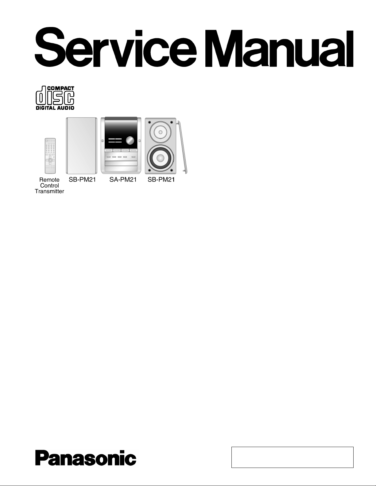
CD Stereo System
SA-PM21PC
Colour
(S)... Silver Type
ORDER NO. MD0501013C1
A6
Specification
n Amplifier Section
FTC Output Power both channel driven
10% total harmonic distortion
20 Hz - 3.5 kHz (Low channel) 15 W per channel (6 Ω)
3.5 kHz - 20 kHz (High channel) 5 W per channel (6 Ω)
RMS Output Power both channel driven
10% total harmonic distortion
1 kHz (Low channel) 15 W per channel (6 Ω)
8 kHz (High channel) 5 W per channel (6 Ω)
Total Bi-Amp power 20 W per channel
Output impedance
Headphone 16 Ω -32Ω
n FM Tuner Section
Frequency range 87.5 MHz -108.0 MHz
(100 kHz step)
87.9 MHz - 107.9 MHz
(200 kHz step)
Sensitivity 1.5 µV (IHF)
S/N 26 dB 1.25 µV
ntenna terminals 75 Ω (unbalanced)
n AM Tuner Section
Frequency range 520 kHz - 1710 kHz (10 kHz step)
Sensitivity
S/N 20 dB (at 1000 kHz) 500 µV/m
n Cassette Deck Section
Track system 4 track, 2 channel
Heads
Record/playback Solid permalloy head
Erasure AC erase head
Motor DC servo moto
Recording system AC bias 100 kHz
Erase system AC erase 100 kHz
Tape speed 4.8cm/s(17/8ips)
Overall frequency response (+3 dB, -6 dB) at DECK OUT
NORMAL 35 Hz - 14 kHz
S/N RATIO 50 dB (A weighted)
Wow and flutter 0.08% (WRMS)
Fast forward and rewind time Approx. 120 seconds with C-60
cassette tape
n CD Section
Disc played
CD/MP3/CD-R/RW 8cm/12cm (3 3/20”/4 73/100”)
Bit rate
MP3 32kbps - 320kbps
Sampling frequency
CD 44.1 kHz
MP3 32 kHz, 44.1 kHz, 48 kHz
Decoding 16 bit linea
© 2005 Matsushita Electric Industrial Co. Ltd.. All
rights reserved. Unauthorized copyin g and
distribution is a violation of law.
Page 2
SA-PM21PC
Pickup
Beam source / wavelength Semiconductor laser / 780nm
Number of channels Stereo
Wow and flutter Below measurable limit
Digital filter 8fs
D/A converter MASH (1 bit DAC)
Frequency response 20Hz - 20 kHz (+1dB, -2dB)
n General
Power supply AC 120 V, 60 Hz
Power consumption 57 W
Dimensions (W x H x D) 165 x 228 x 315.6 mm
(6 1/2” x 9” x 12 7/16”)
Mass 3.6kg(7.9Ibs)
Power consumption in standby
mode
Notes :
1. Specifications are subject to change without notices. Mass and
dimensions are approximate.
2. Total harmonic distortion is measured by the digital spectrum
analyzer.
n System : SC-PM21PC-S Music center: SA-PM21PC-S
Speaker: SB-PM21E-MJ
CONTENTS
Page Page
1 Safety Precautions
1.1. GENERAL GUIDELINES
2 Before Repair and Adjustment
3 Protection Circuitry
4 Handling the Lead-free Solder
4.1. About lead free solder (PbF)
5 Precaution of Laser Diode
6 Handling Precautions For Traverse Deck
7 Accessories
8 Operation Procedures
9 Information on CD & MP3
10 Assembling and Disassembling
10.1. Disassembly flow chart
10.2. Disassembly of Side Panel L & R
10.3. Disassembly of Top Cabinet Unit
10.4. Disassembly of Deck Mechanism and Tape Eject P.C.B
10.5. Disassembly of Headphone P.C.B
10.6. Disassembly of Front Panel Assembly
10.7. Disassembly of Panel P.C.B
10.8. Disassembly of Rear Cabinet
10.9. Disassembly of Tuner Pack
10.10. Disassembly of Main P.C.B
10.11. Disassembly of Powe r P.C.B
10.12. Disassembly of Speak er Termi nal P.C.B
10.13. Disassembly of Trans forme r P.C.B
10.14. Disassembly of CD Mechanism
10.15. Checking Procedure for Each Major P.C.B.
10.16. Procedures of Repla cing Trave rse Base (Unit), Driving
Gear, and Cam Gear (CD Mechanism Unit)
10.17. Procedures for Repla cing Optica l Pickup (CD Mechanism
Unit)
10.18. Procedures for Repla ceme nt Traverse Gear A and
Traverse Gear B (CD Mechanism Unit)
4
4
6
6
6
6
7
8
9
10
11
12
12
13
13
13
14
14
15
15
15
16
16
17
17
18
19
19
22
23
10.19. Procedure for Repla cing Casse tte Holde r
10.20. Procedure for Repla cing Pinch Roller and Head Block
(Deck Mechanism Unit)
10.21. Procedure for Repla cing Motor , Capstan Belt A, Capst an
Belt B, and Winding Belt (Deck Mechanism Unit)
10.22. Procedure for Repla cing Parts on Deck Mechanism PCB
10.23. Handling of casse tte tape jam
11 Service Positions
11.1. Checking procedure
11.2. Checking the major P.C.B.
12 Self Diagnostic Function
12.1. Self-diagnosis Function
12.2. Clearing all error code
12.3. Cancelling the Self-Diagnostic mode
12.4. Setting of doctor mode
13 Procedure for Checking Operation of Individual Parts of Deck
Mechanism Unit
13.1. Operation Check with Cassette Tape
13.2. Operation Check without Cassette Tape
14 Measurement And Adjustments
14.1. Cassette Deck Section
15 Voltage Measurement and Waveform Chart
15.1. Voltage Measureme nt
15.2. Waveform
16 Block Diagram
16.1. CD Servo Block
16.2. Main Block
17 Notes of Schematic Diagram
18 Schematic Diagram
18.1. CD Servo Circuit
18.2. Main Circuit and Tuner Extent Circuit
18.3. Panel Circuit
0.5 W
24
24
25
27
27
29
29
29
30
30
32
32
32
37
37
37
39
39
41
41
43
44
44
46
50
51
51
53
57
2
Page 3
18.4. Deck Circuit, Deck Mechanism Circuit and Tape Eject
Circuit
18.5. Power Circuit
18.6. Transformer Circuit, Headphone Circuit and Speaker
Terminal Circuit
19 Printed Circuit Board
19.1. CD Servo P.C.B.
19.2. Main P.C.B.
19.3. Tuner Extent P.C.B, Headphone P.C.B and Speaker
Terminal P.C.B.
19.4. Panel P.C.B.
19.5. Deck P.C.B and Deck Mechanism P.C.B.
19.6. Power P.C.B.
19.7. Transformer P.C.B and Tape Eject P.C.B.
20 Wiring Connection Diagram
21 Illustration of IC 痴, Transistors and Diodes
22 Terminal Function of ICエs
58
60
22.1. IC702 (MN662795 3HB) Servo processor/ Digital signal
processor/ Digital filter/ D/A converter
61
62
62
63
22.2. IC703 (BA5948FPE2) IC 4CH DRIVE
22.3. IC803 (MN101C49GHA) MICRO PROCESSOR
23 Troubleshooting Flowchart (CD Section Circuit)
24 Parts Location and Replaceme nt Parts List
24.1. Deck Mechanism
65
66
67
68
69
24.2. CD Loading Mechanism
24.3. Cabinet
24.4. Electrical Part List
24.5. Packaging Materials & Accessories Parts List
24.6. Packaging
70
SA-PM21PC
72
73
73
74
75
76
78
79
81
83
86
92
92
3
Page 4
SA-PM21PC
1 Safety Precautions
1.1. GENERAL GUIDELINES
1. When servicing, observe the original lead dress. If a short circuit is found, replace all parts which have been overheated or
damaged by the short circuit.
2. After servicing, ensure that all the protective devices such as insulation barriers, insulation papers shields are properly installed.
3. After servicing, check for leakage current checks to prevent from being exposed to shock hazards.
(This “Safety Precaution” is applied only in U.S.A.)
1. Before servicing, unplug the power cord to prevent an electric shock.
2. When replacing parts, use only manufacturer’s recommended components for safety.
3. Check the condition of the power cord. Replace if wear or damage is evident.
4. After servicing, be sure to restore the lead dress, insulation barriers, insulation papers, shields, etc.
5. Before returning the serviced equipment to the customer, be sure to make the following insulation resistance test to prevent the
customer from being exposed to a shock hazard.
1.1.1. LEAKAGE CURRENT COLD CHECK
1. Unplug the AC cord and connect a jumper between the two prongs on the plug.
2. Using an ohmmeter measure the resistance value, between the jumpered AC plug and each exposed metallic cabinet part on
the equipment such as screwheads, connectors, control shafts, etc. When the exposed metallic part has a return path to the
chassis, the reading should be between 1MΩ and 5.2Ω.
When the exposed metal does not have a return path to the chassis, the reading must be
.
Fig. 1
1.1.2. LEAKAGE CURRENT HOT CHECK (See Figure 1.)
1. Plug the AC cord directly into the AC outlet. Do not use an isolation transformer for this check.
2. Connect a 1.5kΩ, 10 watts resistor, in parallel with a 0.15µF capacitors, between each exposed metallic part on the set and a
good earth ground such as a water pipe, as shown in Figure 1.
3. Use an AC voltmeter, with 1000 ohms/volt or more sensitivity, to measure the potential across the resistor.
4. Check each exposed metallic part, and measure the voltage at each point.
5. Reverse the AC plug in the AC outlet and repeat each of the above measurements.
6. The potential at any point should not exceed 0.75 volts RMS. A leakage current tester (Simpson Model 229 or equivalent) may
be used to make the hot checks, leakage current must not exceed 1/2 milliamp. should the measurement is outside of the limits
specified, there is a possibility of a shock hazard, and the equipment should be repaired and re-checked before it is returned
to the customer.
4
Page 5

1.1.3. Caution for fuse replacement
SA-PM21PC
5
Page 6

SA-PM21PC
2 Before Repair and Adjustment
Disconnect AC power, discharge Power Supply Capacitors C839 & C840 through a 10Ω, 1W resistor to ground.
DO NOT SHORT-CIRCUIT DIRECTLY (with a screwdriver blade, for instance), as this may destroy solid state devices.
After repairs are completed, restore power gradually using a variac, to avoid overcurrent.
· Current consumption at AC 120 V, 60 Hz in NO SIGNAL mode should be ~200 mA.
3 Protection Circuitry
The protection circuitry may have operated if either of the following conditions are noticed:
· No sound is heard when the power is turned on.
· Sound stops during a performance.
The function of this circuitry is to prevent circuitry damage if, for example, the positive and negative speaker connection wires are
"shorted", or if speaker systems with an impedance less than the indicated rated impedance of the amplifier are used.
If this occurs, follow the procedure outlines below:
1. Turn off the power.
2. Determine the cause of the problem and correct it.
3. Turn on the power once again after one minute.
Note:
When the protection circuitry functions, the unit will not operate unless the power is first turned off and then on again.
4 Handling the Lead-free Solder
4.1. About lead free solder (PbF)
Distinction of PbF P.C.B.:
P.C.B.s (manufactured) using lead free solder will have a PbF stamp on the P.C.B.
Caution:
· Pb free solder has a higher melting point than standard solder; Typically the melting point is 50 - 70°F (30 - 40°C) higher. Please
use a high temperature soldering iron. In case of soldering iron with temperature control, please set it to 700 ± 20°F (370 ±
10°C).
· Pb free solder will tend to splash when heated too high (about 1100°F/600°C).
· When soldering or unsoldering, please completely remove all of the solder on the pins or solder area, and be sure to heat the
soldering points with the Pb free solder until it melts enough.
6
Page 7
SA-PM21PC
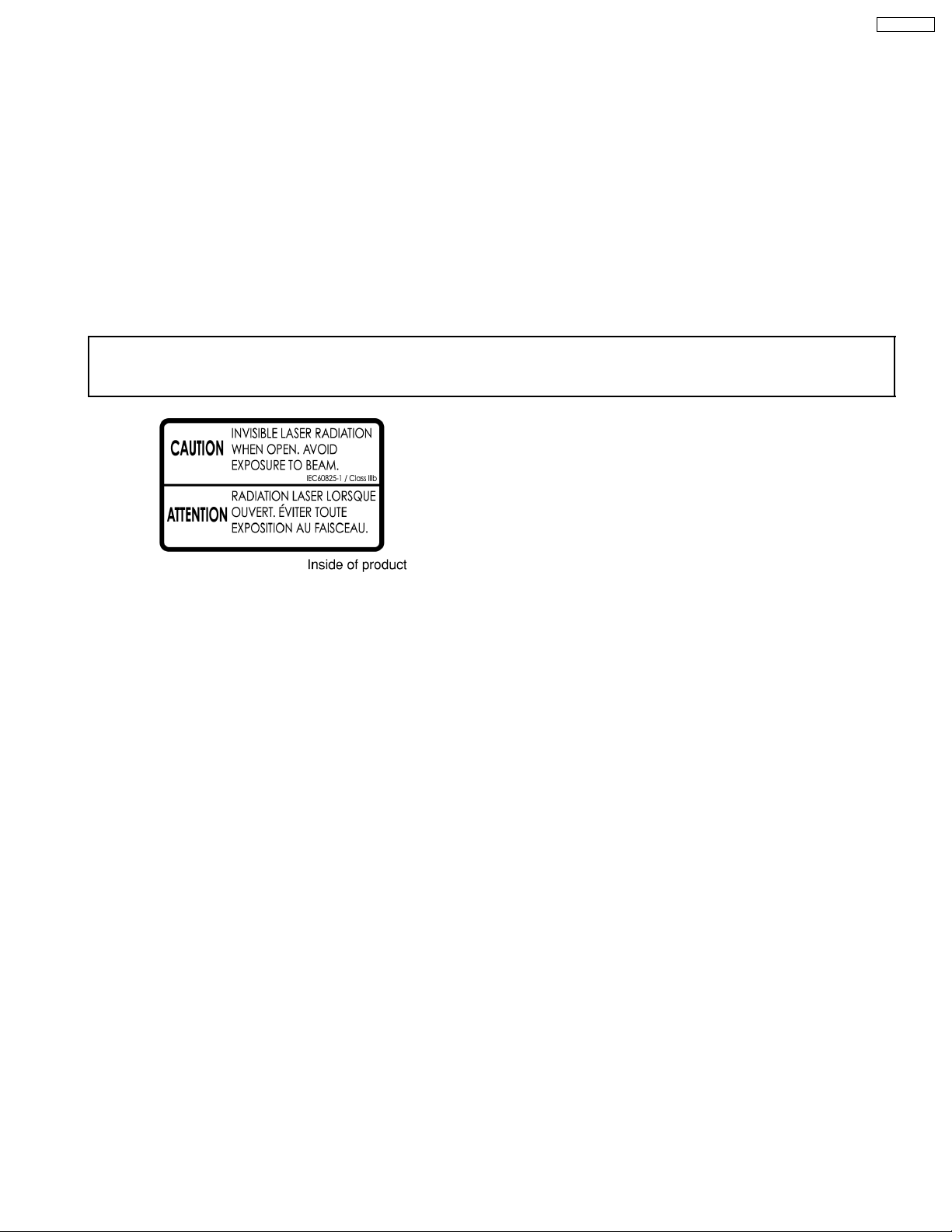
5 Precaution of Laser Diode
CAUTION:
This unit utilizes a class 1 laser.
Invisible laser radiation is emitted from the optical pickup lens.
When the unit is turned on:
1. Do not look directly into the pick up lens.
2. Do not use optical instruments to look at the pick up lens.
3. Do not adjust the preset variable resistor on the pickup lens.
4. Do not disassemble the optical pick up unit.
5. If the optical pick up is replaced, use the manufacturer’s specified replacement pick up only.
6. Use of control or adjustments or performance of procedures other than those specified herein may result in hazardous radiation
exposure.
CAUTION!
THIS PRODUCT UTILIZES A LASER.
USE OF CONTROLS OR ADJUSTMENTS OR PERFORMANCE OF PROCEDURES OTHER THAN THOSE SPECIFIED HEREIN MAY RESULT
IN HAZARDOUS RADIATION EXPOSURE.
7
Page 8
SA-PM21PC
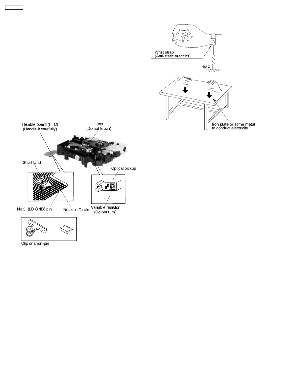
6 Handling Precautions For Traverse Deck
The laser diode in the traverse deck (optical pickup) may break
down due to potential difference caused by static electricity of
clothes or human body.
So, be careful of electrostatic breakdown during repair of the
traverse deck (optical pickup).
l Handling of CD traverse deck (optical pickup)
1. Do not subject the traverse deck (optical pickup) to
static electricity as it is extremely sensitive to electrical
shock.
2. The short land between the No.4 (LD) and No.5 (GND)
pins on the flexible board (FFC) is shorted with a solder
build-up to prevent damage to the laser diode.
3. Take care not to apply excessive stress to the flexible
board (FFC board) (Fig 6.1).
4. Do not turn the variable resistor (laser power
adjustment). It has already been adjusted.
Fig 6.2
Fig 6.1
l Grounding for electrostatic breakdown prevention
1. Human body grounding (Fig 6.2)
Use the anti-static wrist strap to discharge the static
electricity from your body.
2. Work table grounding (Fig 6.2)
Put a conductive material (sheet) or steel sheet on the
area where the traverse deck (optical pickup) is placed,
and ground the sheet.
Caution :
The static electricity of your clothes will not be grounded
through the wrist strap. So, take care not to let your
clothes touch the traverse deck (optical pickup).
Caution when Replacing the Optical Pickup :
The traverse has a short point shorted with solder to protect
the laser diode against electrostatics breakdown. Be sure to
remove the solder from the short point before making
connections.
8
Page 9

7 Accessories
Note : Refer to Packing Materials & Accessories (Section 24.5) for part number.
Remote control
AC cord
FM indoor
antenna
SA-PM21PC
AM loop antenna
9
Page 10
SA-PM21PC
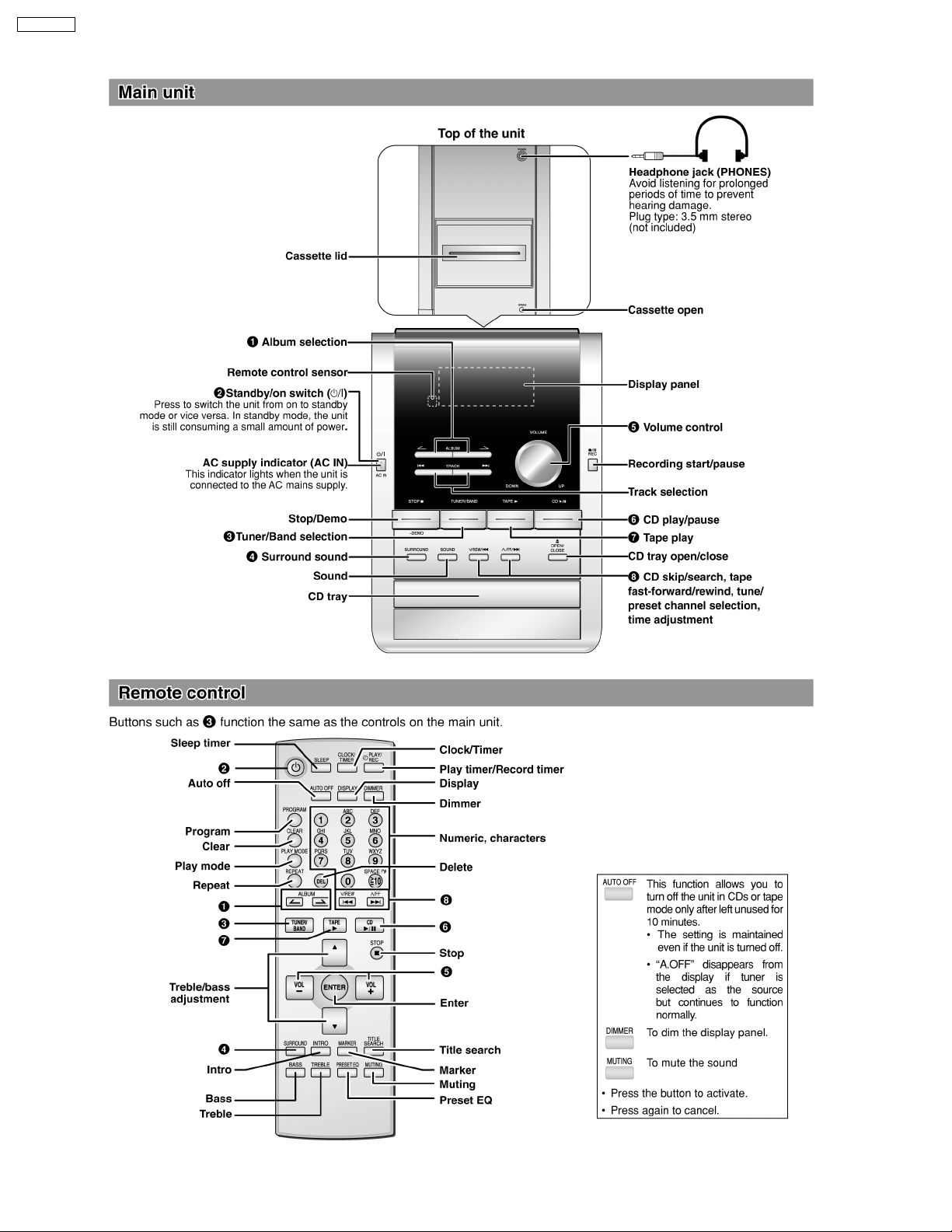
8 Operation Procedures
10
Page 11
9 Information on CD & MP3
SA-PM21PC
11
Page 12
SA-PM21PC
10 Assembling and Disassembling
“ATTENTION SERVICER”
Some chassis components may be have sharp edges. Be careful when disassembling and servicing.
1. This section describes procedures for checking the operation of the major printed circuit boards and replacing the main
components.
2. For reassembly after operation checks or replacement, reverse the respective procedures.
Special reassembly procedures are described only when required.
3. Select items from the following index when checks or replacement are required.
Warning:
This product uses a laser diode. Refer to “Precaution of Laser Diode”.
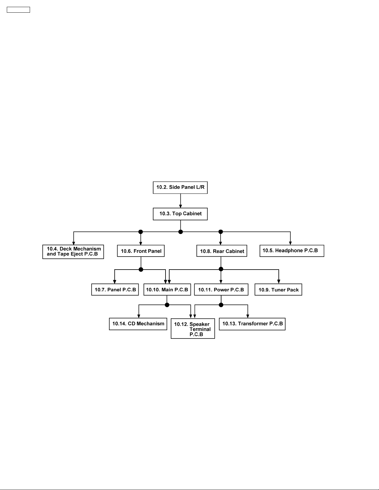
10.1. Disassembly flow chart
The following chart is the procedure for disassembling the casing and inside parts for internal inspection when carrying out the
servicing.
To assemble the unit, reverse the steps shown in the chart below.
12
Page 13

10.2. Disassembly of Side Panel L &
R
Step 1 : Remove 4 screws.
Step 2 : Remove 1 screw.
Step 3 : Remove the side panel (R) as arrow shown (Be careful
of the catches).
SA-PM21PC
Step 1 : Remove 1 screw.
Step 2 : Release catches at both ends.
Step 3 : Lift up the top cabinet unit, push backward as arrow
shown and flip top cabinet unit sideway.
Step 4 : Remove 4 screws.
Step 5 : Remove 1 screw.
Step 6 : Remove the side panel (L) as arrow shown (Be careful
of the catches).
10.3. Disassembly of Top Cabinet
Unit
· Follow the (Step 1) - (Step 6) of Item 10.2.
Step 4 : Detach the connectors CN504A and FFC CN804.
10.4. Disassembly of Deck
Mechanism and Tape Eject
P.C.B
· Follow the (Step 1) - (Step 6) of Item 10.2.
· Follow the (Step 1) - (Step 4) of Item 10.3.
13
Page 14
SA-PM21PC
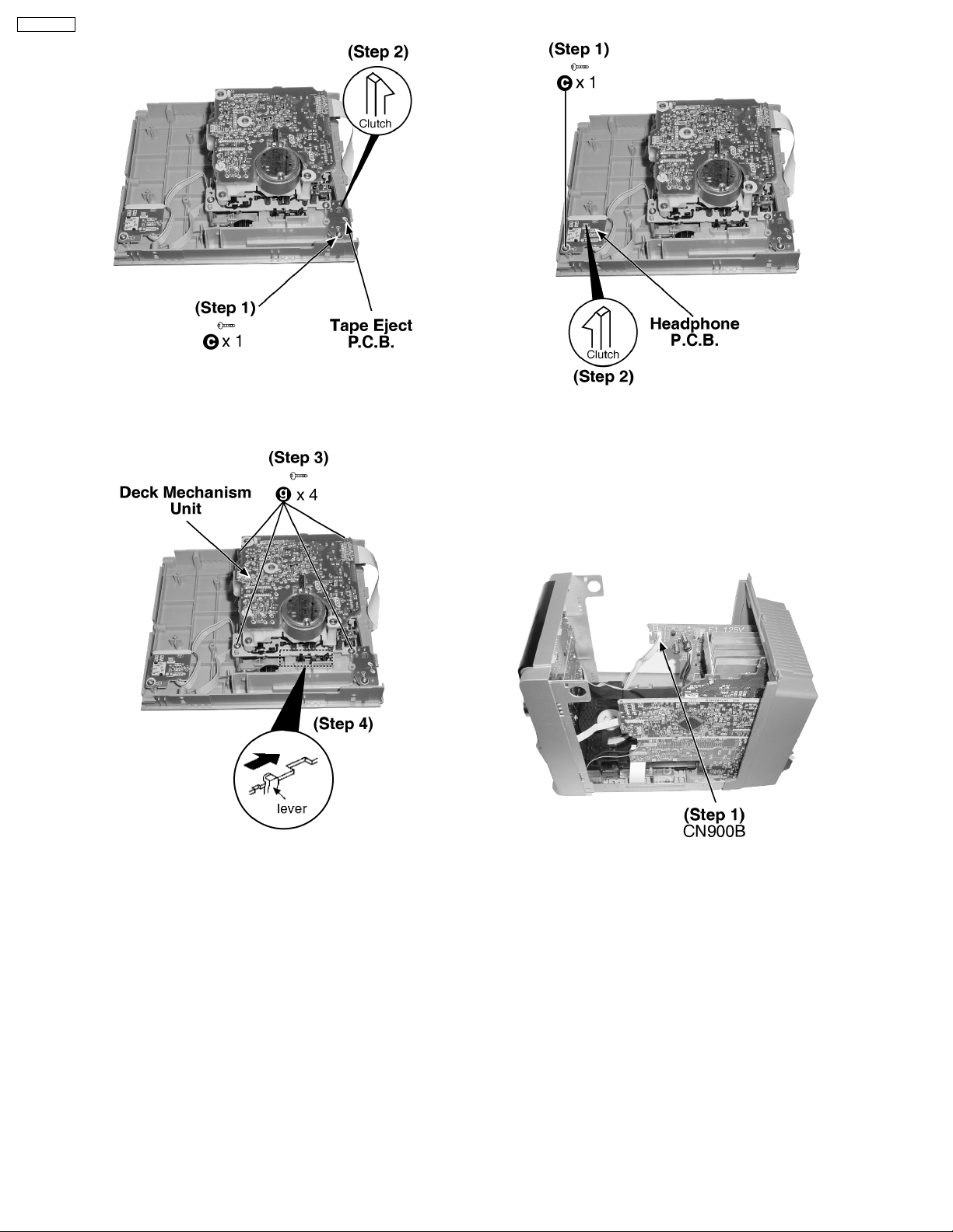
Step 1 : Remove 1 screw.
Step 2 : Release the clutch.
Step 1 : Remove 1 screw.
Step 2 : Release the clutch.
10.6. Disassembly of Front Panel
Assembly
Step 3 : Remove 4 screws.
Step 4 : Push the lever as arrow shown to open the cassette lid
and remove the deck mechanism unit.
10.5. Disassembly of Headphone
P.C.B
· Follow the (Step 1) - (Step 6) of Item 10.2.
· Follow the (Step 1) - (Step 4) of Item 10.3.
Step 1 : Detach the connector CN900B .
· Follow the (Step 1) - (Step 6) of Item 10.2.
· Follow the (Step 1) - (Step 4) of Item 10.3.
14
Page 15
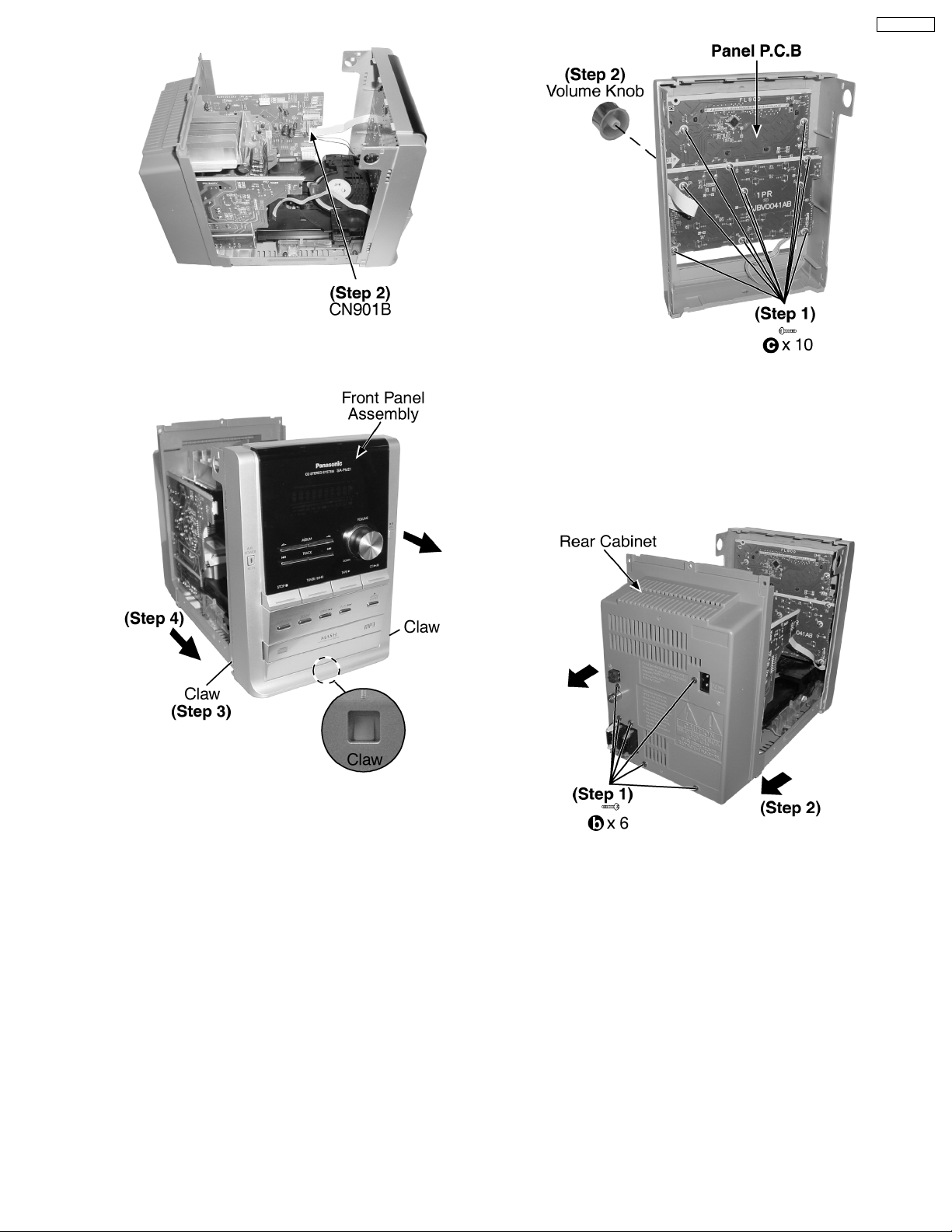
Step 2 : Detach the FFC CN901B.
SA-PM21PC
Step 1 : Remove 10 screws.
Step 2 : Remove the Volume Knob.
10.8. Disassembly of Rear Cabinet
· Follow the (Step 1) - (Step 6) of Item 10.2.
· Follow the (Step 1) - (Step 4) of Item 10.3.
Step 3 : Release 3 Claws.
Step 4 : Remove the front panel assembly as arrow shown.
10.7. Disassembly of Panel P.C.B
· Follow the (Step 1) - (Step 6) of Item 10.2.
· Follow the (Step 1) - (Step 4) of Item 10.3.
· Follow the (Step 1) - (Step 4) of Item 10.6.
Step 1 : Remove 6 screws.
Step 2 : Remove the rear cabinet as arrow shown.
10.9. Disassembly of Tuner Pack
· Follow the (Step 1) - (Step 6) of Item 10.2.
· Follow the (Step 1) - (Step 4) of Item 10.3.
· Follow the (Step 1) - (Step 2) of Item 10.8.
15
Page 16
SA-PM21PC
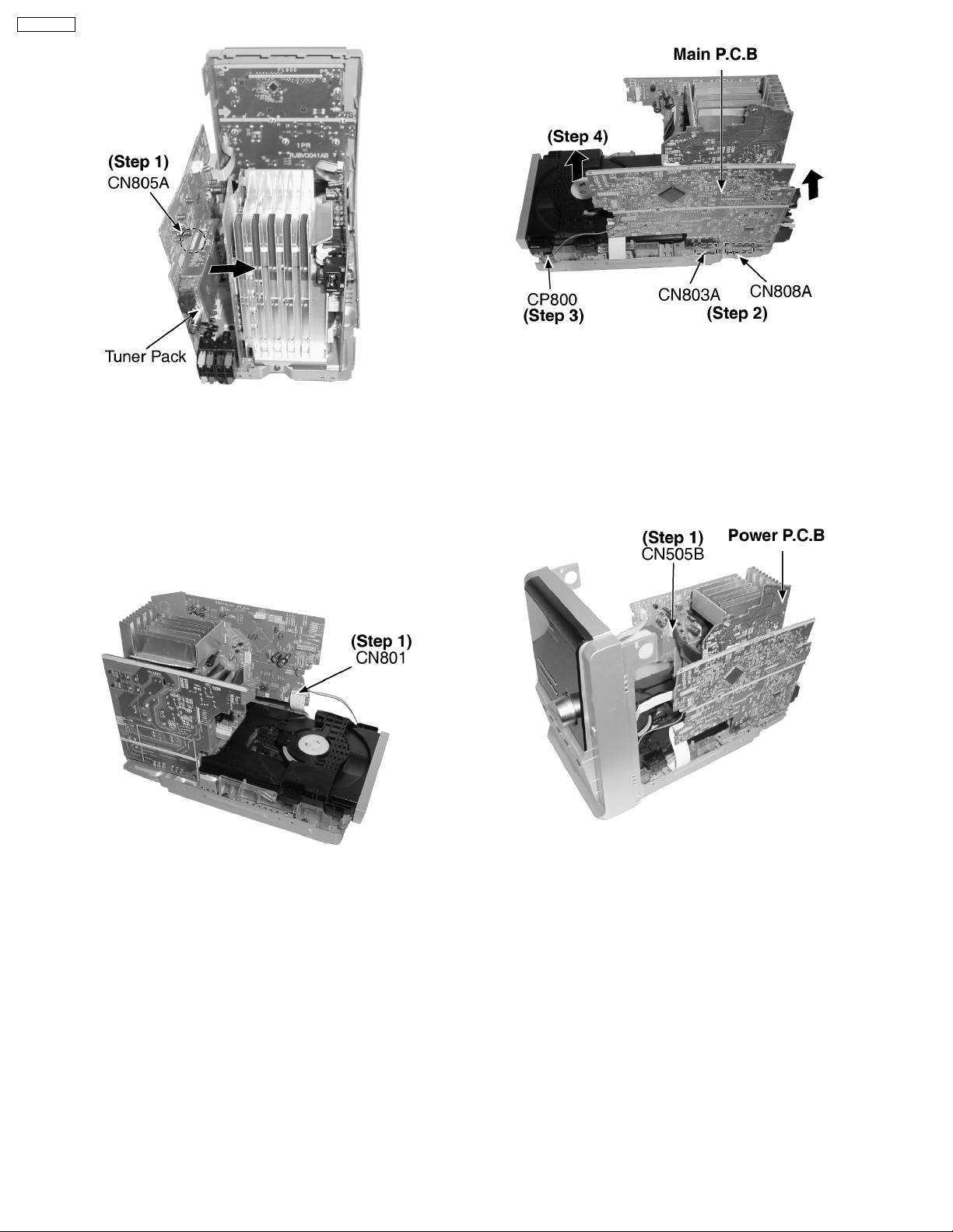
Step 1 : Detach the connector CN805A and remove the tuner
pack as arrow shown.
10.10. Disassembly of Main P.C.B
· Follow the (Step 1) - (Step 6) of Item 10.2.
· Follow the (Step 1) - (Step 4) of Item 10.3.
· Follow the (Step 1) - (Step 4) of Item 10.6.
· Follow the (Step 1) - (Step 2) of Item 10.8.
Step 2 : Detach the connector CN803A, CN808A.
Step 3 : Detach the connector CP800.
Step 4 : Remove the Main P.C.B as arrow shown.
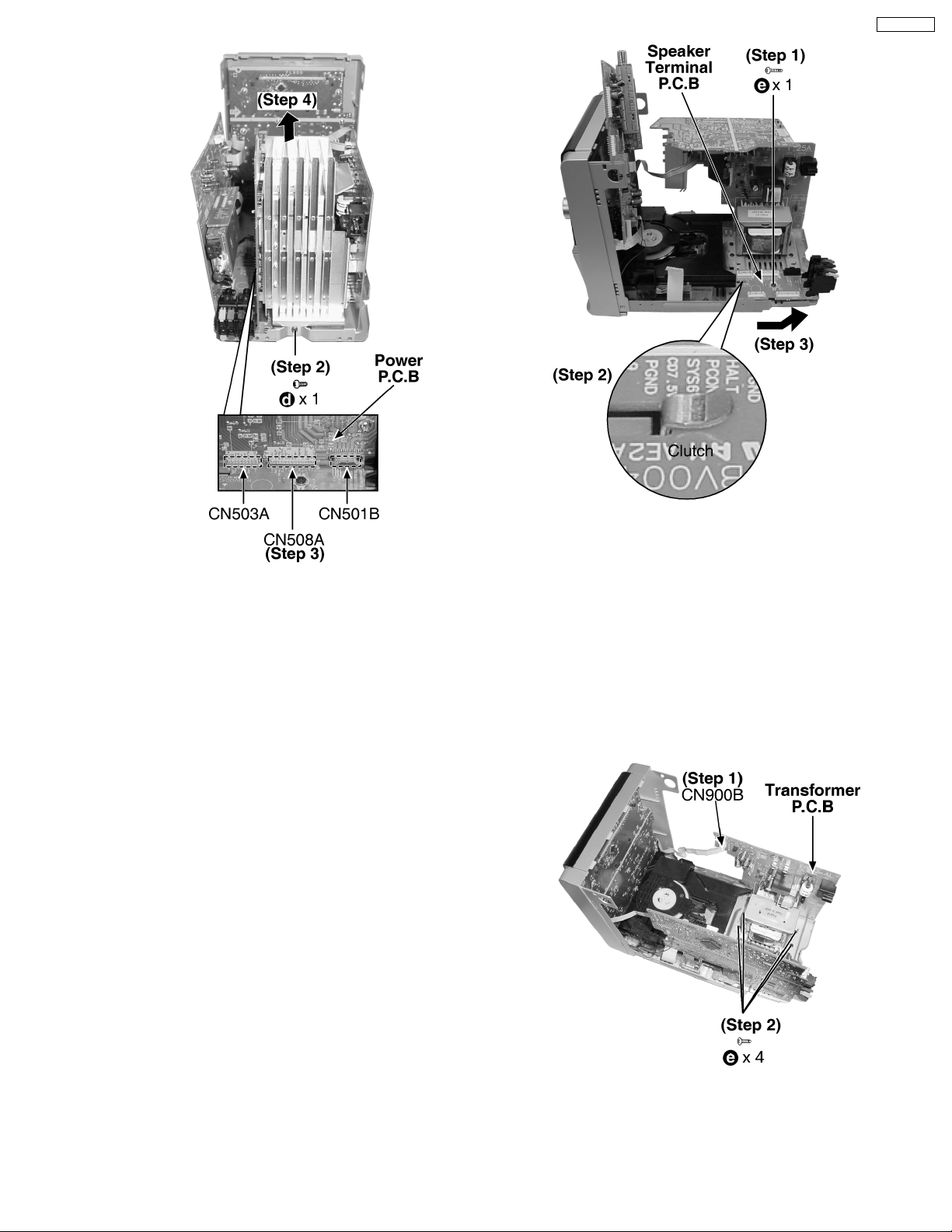
10.11. Disassembly of Power P.C.B
· Follow the (Step 1) - (Step 6) of Item 10.2.
· Follow the (Step 1) - (Step 4) of Item 10.3.
· Follow the (Step 1) - (Step 2) of Item 10.8.
Step 1 : Detach the FFC CN801.
Step 1 : Detach the connector CN505B.
16
Page 17
SA-PM21PC
Step 2 : Remove 1 screw.
Step 3 : Detach the connector CN503A, CN508A, CN501B.
Step 4 : Remove the Power P.C.B as arrow shown.
10.12. Disassembly of Speaker
Terminal P.C.B
· Follow the (Step 1) - (Step 6) of Item 10.2.
· Follow the (Step 1) - (Step 4) of Item 10.3.
· Follow the (Step 1) - (Step 2) of Item 10.8.
· Follow the (Step 1) - (Step 2) of Item 10.10.
· Follow the (Step 2) - (Step 4) of Item 10.11.
Step 1 : Remove 1 screw.
Step 2 : Release the clutch.
Step 3 : Remove the Speaker Terminal P.C.B as arrow shown.
10.13. Disassembly of Transformer
P.C.B
· Follow the (Step 1) - (Step 6) of Item 10.2.
· Follow the (Step 1) - (Step 4) of Item 10.3.
· Follow the (Step 1) - (Step 2) of Item 10.8.
· Follow the (Step 1) - (Step 4) of Item 10.11.
Step 1 : Detach the connector CN900B.
Step 2 : Remove 4 screws.
17
Page 18
SA-PM21PC
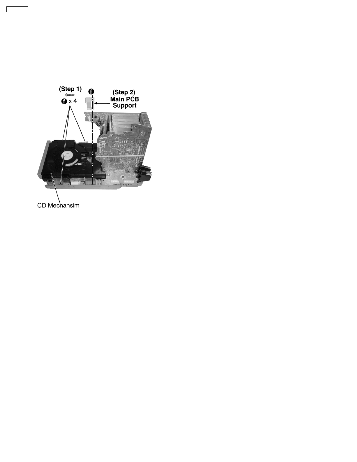
10.14. Disassembly of CD
Mechanism
· Follow the (Step 1) - (Step 6) of Item 10.2.
· Follow the (Step 1) - (Step 4) of Item 10.3.
· Follow the (Step 1) - (Step 4) of Item 10.6.
· Follow the (Step 1) - (Step 2) of Item 10.8.
· Follow the (Step 1) - (Step 4) of Item 10.10.
Step 1 : Remove 4 screws.
Step 2 : Remove the Main P.C.B Support.
18
Page 19
10.15. Checking Procedure for Each
Major P.C.B.
10.15.1. Replacement of the Power
Amplifier IC
· Replacement of the Power Amplifier IC
· Follow the (Step 1) - (Step 6) of Item 10.2.
· Follow the (Step 1) - (Step 4) of Item 10.3.
· Follow the (Step 1) - (Step 2) of Item 10.8.
· Follow the (Step 1) - (Step 4) of Item 10.11.
SA-PM21PC
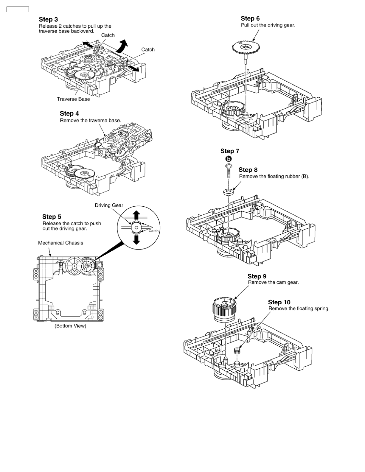
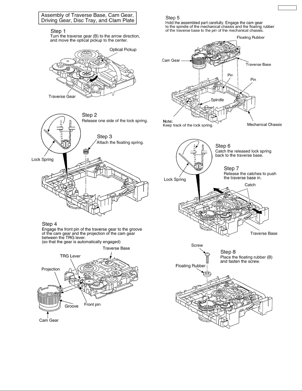
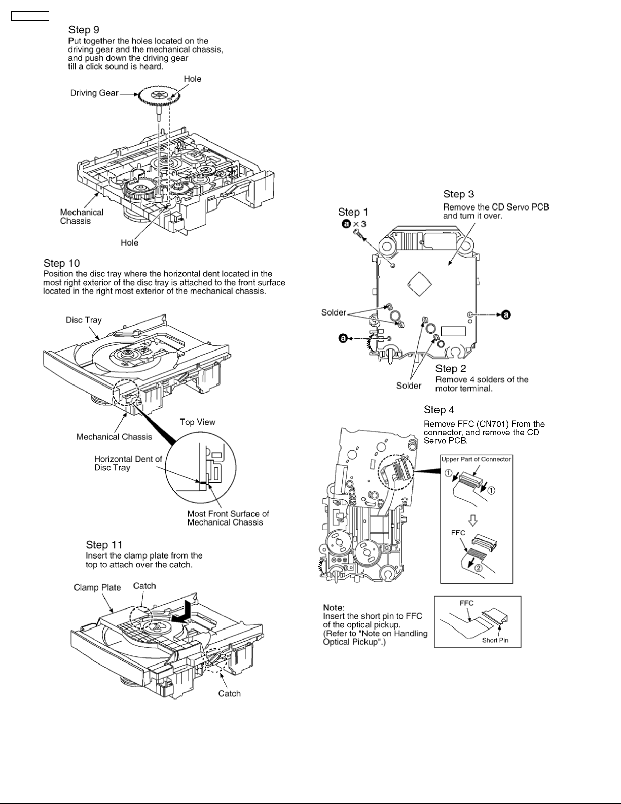
10.16. Procedures of Replacing
Traverse Base (Unit), Driving
Gear, and Cam Gear (CD
Mechanism Unit)
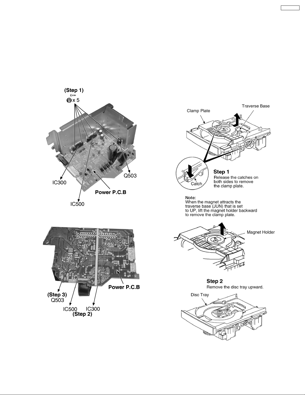
10.16.1. Disassembly of the Disc Tray.
· Follow the (Step 1) - (Step 6) of Item 10.2.
· Follow the (Step 1) - (Step 4) of Item 10.3.
· Follow the (Step 1) - (Step 4) of Item 10.6.
· Follow the (Step 1) - (Step 2) of Item 10.8 .
· Follow the (Step 1) - (Step 4) of Item 10.10.
· Follow the (Step 1) - (Step 2) of Item 10.14.
Step 1 Remove 5 screws.
Step 2 Unsolder the terminals of Power Amp IC (IC300, IC500)
and replace the component.
Step 3 Unsolder the terminals of Transistor (Q503) and replace
the component.
19
Page 20
SA-PM21PC
20
Page 21
SA-PM21PC
21
Page 22
SA-PM21PC
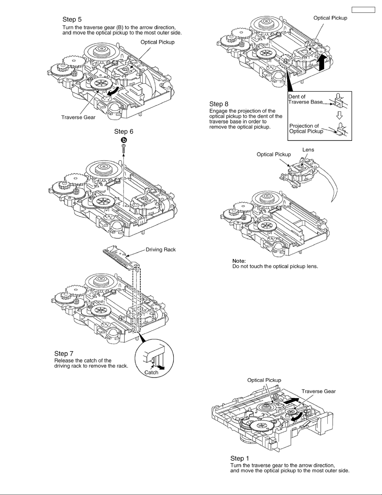
10.17. Procedures for Replacing
Optical Pickup (CD Mechanism
Unit)
· Follow the (Step 1) - (Step 6) of Item 10.2.
· Follow the (Step 1) - (Step 4) of Item 10.3.
· Follow the (Step 1) - (Step 4) of Item 10.6.
· Follow the (Step 1) - (Step 2) of Item 10.8.
· Follow the (Step 1) - (Step 4) of Item 10.10.
· Follow the (Step 1) - (Step 2) of Item 10.14.
· Follow the (Step 1) - (Step 4) of Item 10.16.1.
22
Page 23
SA-PM21PC
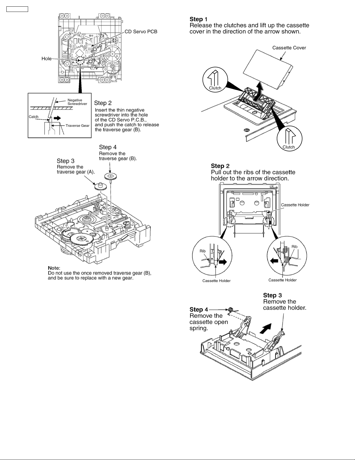
10.18. Procedures for Replacement
Traverse Gear A and Traverse
Gear B (CD Mechanism Unit)
· Follow the (Step 1) - (Step 6) of Item 10.2.
· Follow the (Step 1) - (Step 4) of Item 10.3.
· Follow the (Step 1) - (Step 4) of Item 10.6.
· Follow the (Step 1) - (Step 2) of Item 10.8.
· Follow the (Step 1) - (Step 4) of Item 10.10.
· Follow the (Step 1) - (Step 2) of Item 10.14.
· Follow the (Step 1) - (Step 2) of Item 10.16.1.
23
Page 24
SA-PM21PC
10.19. Procedure for Replacing
Cassette Holder
· Follow the (Step 1) - (Step 6) of Item 10.2.
· Follow the (Step 1) - (Step 4) of Item 10.3.
· Follow the (Step 1) - (Step 4) of Item 10.4.
10.20. Procedure for Replacing Pinch
Roller and Head Block (Deck
Mechanism Unit)
· Follow the (Step 1) - (Step 6) of Item 10.2.
· Follow the (Step 1) - (Step 4) of Item 10.3.
24
Page 25
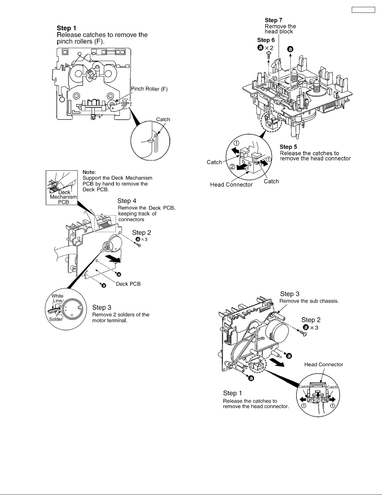
· Follow the (Step 1) - (Step 4) of Item 10.4.
SA-PM21PC
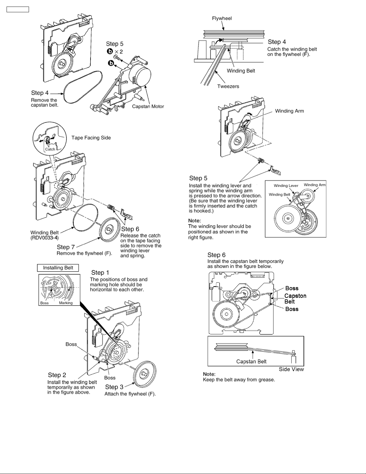
10.21. Procedure for Replacing
Motor, Capstan Belt A,
Capstan Belt B, and Winding
Belt (Deck Mechanism Unit)
· Follow the (Step 1) - (Step 6) of Item 10.2.
· Follow the (Step 1) - (Step 4) of Item 10.3.
· Follow the (Step 1) - (Step 4) of Item 10.4.
· Follow the (Step 1) - (Step 4) of Item 10.20.
25
Page 26
SA-PM21PC
26
Page 27
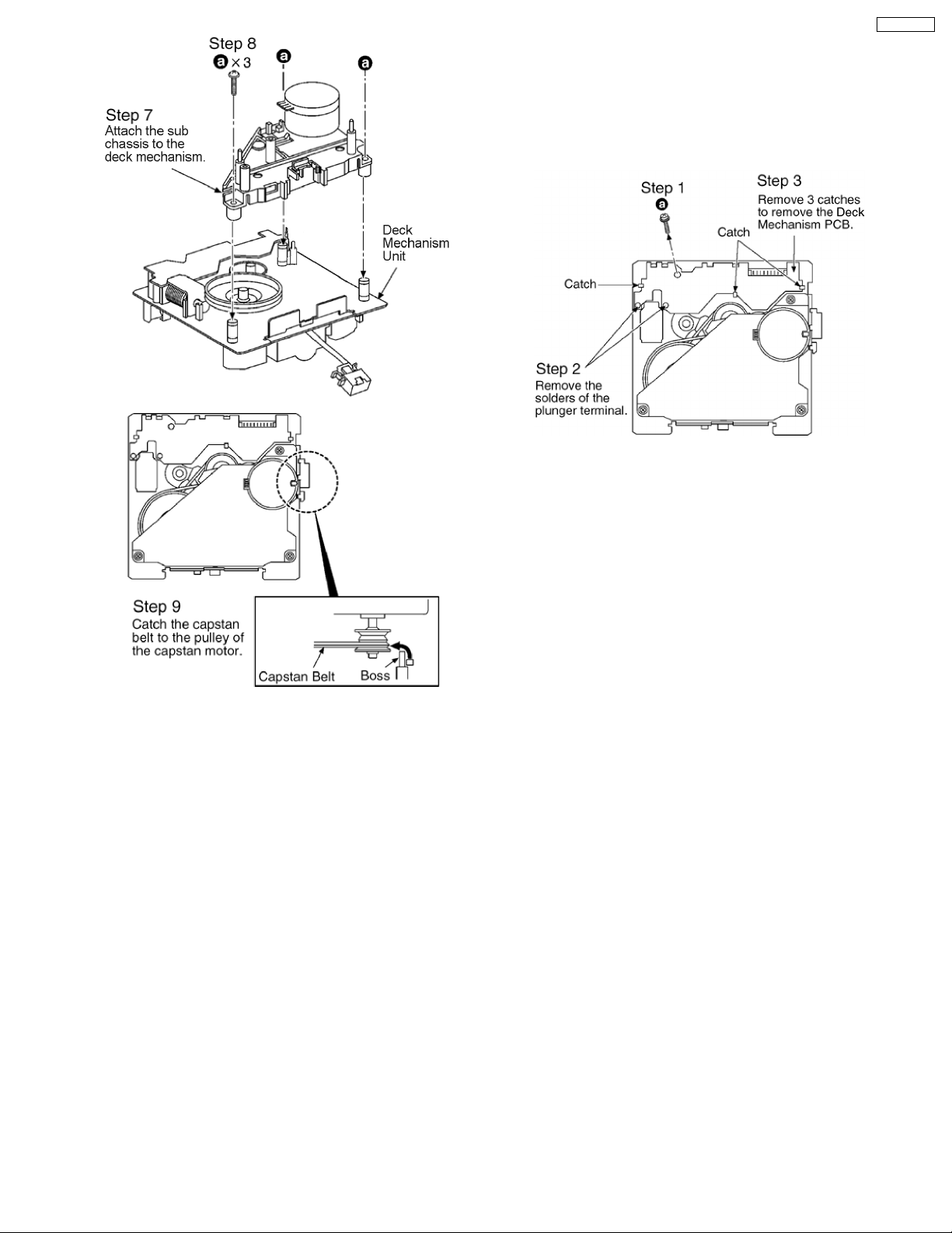
10.22. Procedure for Replacing Parts
on Deck Mechanism PCB
· Follow the (Step 1) - (Step 6) of Item 10.2.
· Follow the (Step 1) - (Step 4) of Item 10.3.
· Follow the (Step 1) - (Step 4) of Item 10.4.
SA-PM21PC
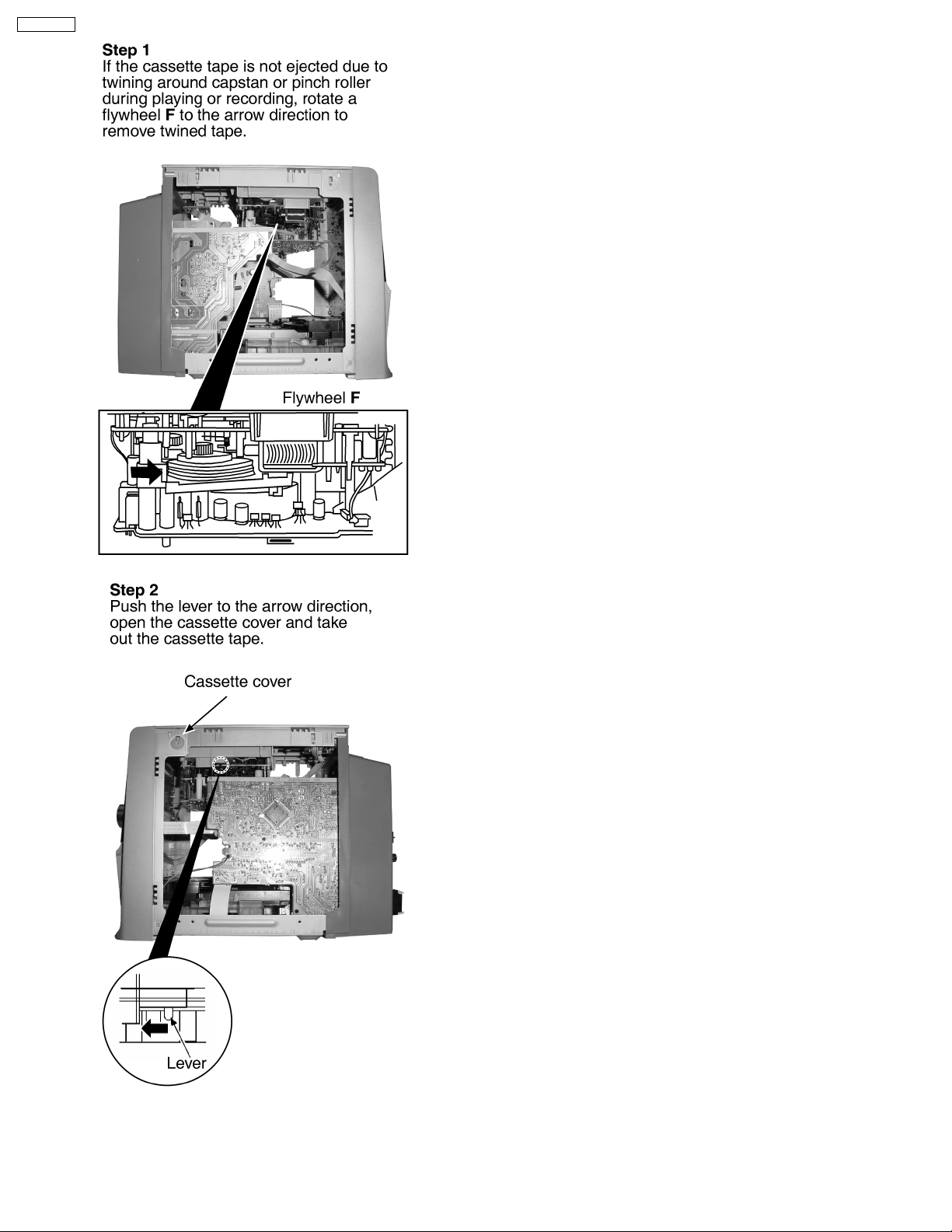
10.23. Handling of cassette tape jam
· Follow the (Step 1) - (Step 6) of Item 10.2.
27
Page 28
SA-PM21PC
28
Page 29

11 Service Positions
11.1. Checking procedure
Note:
For the disassembling procedure, see the section 10.
11.2. Checking the major P.C.B.
SA-PM21PC
1. Disassembly of Side Panel L & R
2. Disassembly of Top Cabinet
3. Disassembly of Deck Mechanism P.C.B and Tape Eject
P.C.B.
4. Disassembly of Headphone P.C.B.
5. Disassembly of Front Panel
6. Disassembly of Panel P.C.B.
7. Disassembly of Rear Cabinet
8. Disassembly of Tuner Pack
9. Disassembly of Main P.C.B.
10. Disassembly of Power P.C.B.
11. Disassembly of Speaker Terminal P.C.B.
12. Disassembly of Transformer P.C.B.
13. Disassembly of CD Mechanism
Service tools
Extension cable
(Main P.C.B. and Speaker
Terminal P.C.B.)
RFKPM21
29
Page 30

SA-PM21PC
12 Self Diagnostic Function
12.1. Self-diagnosis Function
12.1.1. Entering into self-diagnosis mode
1. Turn the power on.
2. Switch to CD
3. Press and hold the [STOPn] key of the main set for more than 2 seconds. While pressing this key, press the FF key on the main
set for another 2 seconds to enter into the self-diagnosis mode. The FL will display : [TEST_ _xxx]
Note:
Even if [STOPn] key of the main set is pressed while the self diagnosis mode is on, function will not be switched. Instead,
confirmation of error numbers will begin.
12.1.2. Display Location
mode with no CD or cassette loaded.
Figure 12-1
12.1.3. Error Code Display
· At the self-diagnosis mode, error codes will be displayed when [STOPn] key at the main unit is pressed.
Note:
Error numbers display is due to error symptom encountered during normal operation of unit. These error codes will be
“remembered” and stored.
· Example: [TEST_ _H01] (the display shall be retained)
· To exit from the self-diagnosis mode, execute power OFF operation.
· Even at power OFF operation, this error numbers shall not be cleared (the number can be cleared only at the start up of micro-
p after reset).
· If repeating self-diagnosis, add the newly detected errors only without deleting errors which have been detected before.
12.1.4. Self-diagnosis mode Deck Mechanism
· Activate the Self Diagnosis mode for the Deck and the following Self Diagnosis will be conducted.
Error Code Description
H01: If MODE SW abnormal is detected during normal operation, it will be memorized. The detection and memory
H02: REC INH SW abnormal.
H03: HALF SW abnormal.
F01: Reel pulse abnormal.
F02: TPS abnormal.
· Operating Procedures
1. Activate the self diagnosis mode with the deck unloaded.
2. The test mode displayed will be made and detection shall be executed to check RECINH SW, HALF SW are in the OFF state.
3. Slot a cassette tape (with recording preventive tab present) into the deck and loading the cassette (HALF SW = ON).
4. After this instant with the cassette loaded in, RECINH SW, HALF SW will be checked and confirmed at this stage by the
software. Press FF key to proceed the self-diagnosis. The FF operation will stop automatically after 3 seconds. If abnormal
operation is detected, the tape will stop automatically after 1 second. During the FF operation, the Reel Pulse will be checked
shall be done for Deck.
30
Page 31

SA-PM21PC
by the software.
5. After the tape stops, the Error codes will be displayed by toggling the STOPn key. For more detail explanation, refer to the
(Figure 12-2).
Figure 12-2
No. Operation Procedures Micon operation & processing
1 C-mecha Abnormal Detection shall be
executed for DECK 1 only.
2 [ ] key is pressed, after loading in a
NORMAL type cassette with the recording tab
on the left side removed.
Check that all DECK mechanism leaf SW are in OFF state.
FF shall be executed for 2 sec, afterwhich STOP.
Check the following.
{ F.REC INH SW } is OFF
{ HALF SW } is ON
Reel pulse toggles between H & L.
31
Page 32

SA-PM21PC
No. Operation Procedures Micon operation & processing
3 [ ] key is pressed, after loading a NORMAL,
CrO2, METAL type cassette with the recording
tab on the right side removed.
4 [TAPE ] Key is pressed, after loading in a
NORMAL, CrO2, METAL type cassette (
cassette for TPS checking purposes and with
both recording tabs intact ).
5 [REC] key is pressed, after loading in a
NORMAL type cassette ( with both recording
tabs intact )
6 Self-diagnostic mode is stopped by pressing
the [STOPn] Key.
7 To clear all the abnormalities in the memory,
press the [STOPn] Key for more than 5 Sec
while the self-diagnostic mode is stopped.
8 To cancel the self-diagnostic mode press the
[POWER] Key.
REW shall be executed for 2 sec, afterwhich STOP.
Check the following.
{ F.REC INH SW } is ON
{ HALF SW } is ON
Reel pulse toggles between H & L.
TPS operation is executed. Check the following.
{ F.REC INH SW } is ON
{ HALF SW } is ON
TPS signal changes.
After checking TPS, it shall STOP.
If TPS checking is completed at TAPE END, it is considered as TPS
abnormal.
REC operation shall not be executed.
Check the following.
{ F.REC INH SW } is ON
{ HALF SW } is ON
LCD shall display the abnormality item code, when the STOP key is pressed,
it shall display the abnor mality item code in the following sequence.
[ TEST H 0 1 ] [ TEST H 0 2 ] [ TEST H 0 3 ]
At this time, all the abnormalities item in the memory is cleared and is
displayed on the LCD.[ C L E A R ] display for 1 Sec. then,[ TEST ] is
displayed.
POWER is OFF.At the next POWER ON, normal operation shall be executed.
· As HALF SW solder point and RECINH SW solder point are located close to each other, it’s necessary to check the shorting
between the adjacent points. For this purpose, operation has to be executed twice using two kind of cassettes, i.e. a cassette
with recording preventive tabs for both Sides A/B and a cassette with a recording preventive tab for only either one side of Side
A/B.
12.1.5. Error Code for CD Mechanism
Error code Possible symptom Possible cause
H01 DECK opera tion
abnormal (reel motor,
solenoid, and MODE
SW)
F15 CD REST_SW
abnormal
H15 CD OPEN_SW
abnormal
F26 Communication
between CD servo LSI
and microp abnormal
· During normal operation, if mechanism error process is executed once by mode switch against the
same deck operation, it is judged as mechanism abnormality and this is memorized as an error.
· Conditions for judging mechanism error:
− Mode switch ON is not detected 800 ms after plunger activation for PLAY / REC process.
− Mode switch ON is not detected 800 ms after plunger activation for FF / REW process. Or, Mode
switch OFF is not detected 800 ms after plunger activation after detecting Mode SW ON. Or,
Mode Switch ON is not detected 800 ms after detecting Mode switch OFF.
− If Mode switch comes ON at STOP / PAUSE state (normal condition), this is judged as an Error:
1. Main purpose for this Self Diagnosis is to diagnose a partial short of the deck.
2. Mechanical error process caused by EJECT operation will not be counted.
3. This error number can be cleared only at the start up of micro-p reset.
· At initial setting of CD traverse position, if REST SW ON is not detected even though the fail safe
timer time is over (10 sec), this is memorized as an error and the error number can be cleared only
at the start up of micro-p after reset.
· During normal operation, if CD OPEN SW ON is not detected within 4 sec, then H15 will be
memorized in memory. The error code can be cleared only at the start up of micro-p after reset.
· At the time of switching to CD function, SENSE = H will be detected using DTMS system setting
command. If the error is memorized when SENSE = L is not detected within fail safe timer time (20
sec), [F26] will be displayed simultaneously. This display will be retained if the power is ON and at
CD function. If this error occurs, CD operation afterward cannot be executed as in the case of
[NO.DISC.].
· This error number can be cleared only at the start up of micro-p after reset.
12.2. Clearing all error code
1. Press and hold STOP button for 5 seconds.
2. FL indicator shows “CLEAR” for 1 second and change to “TEST”.
12.3. Cancelling the Self-Diagnostic mode
1. Press the “Power” button to turn off the system. Press the “Power” button again to turn on the system.
12.4. Setting of doctor mode
1. At any more (CD, TAPE, TUNER).
32
Page 33

SA-PM21PC
2. Press and hold [STOPn] button for at least 2 seconds, follow by [4] and [7] from the remote control.
3. When the Doctor Mode is activated the FL display will show the
symbol at the 5thdigit. At the same time, the micro-p’s
version number (base 10) and EEPROM’s checksum (base 16) will be displayed for 1 sec. After displaying the EEPROM
information for 1 sec, the display will return to the normal Doctor mode display
4. However, if the EEPROM was not detected, it will not display the EEPROM’s checksum information . The FL will display microp’s version for 1 sec and return to normal Doctor Mode display.
Note:
Within the Doctor Mode display, at any of the test modes, if input [4] and [7] from the remote control while press [STOPn]of
main set, the micro-p’s version number and EEPROM information will be displayed for 1 sec and then returned to the normal
doctor mode display.
12.4.1. Inspection item list
Test Number Test Item Operation keys (Remote Controller Keys)
1 CD Unit Loading Test [ 10], [1], [1]
2 CD Unit Traverse Test [ 10], [1], [2]
3 CD Unit Combination Test [ 10], [1], [2]
4 EEPROM Checksum Check [DOCTOR MODE] (C2DF) ; [4] + [7]
5 Cold Start Setting [SLEEP]
Note:
· If entering Doctor Mode by numeric buttons, PRESET EQ and SURROUND will be set to OFF.
· In case of error, all the segments of FL will blink (0.5 sec ON/OFF) and Doctor Mode shall be retained.
· The operation key used for the test follows closely with the test items as far as possible to facilitate quick testing to be
carried out.
· The [STOPn] key on the remote controller when used in any test mode will end the current test operations.
· All keys mentioned to initiate Doctor Mode’s test items refer to remote controller keys, unless otherwise mentioned.
· When plugging out from Doctor Mode and then plugging in back. It will reset start.
· The test cancellation special key [0] will end the current test operations but it will remain in Doctor Mode. When used, the
display shows the word [CANCEL] for 2sec, and then returns to Doctor Mode display.
12.4.2. CD Unit Loading Test (Reliability test 1)
· Putpose : To test CD Unit Loading (OPEN / CLOSE aging test) function.
− The following operation will be carried out.
· Procedures :
1. Enter into doctor mode (Refer to section 12.4)
2. Press [
10] followed by [1] & [1] on the remote control.
33
Page 34

SA-PM21PC
3. After a few times, the FL shall display as below:
Special Note:
Due to certain reasons, when the following conditions occur, the aging will stop but the count value shall be maintained:
· During OPEN operation, after a certain timing, the CD does not open in the Open position. (After REST SW is OFF, the CD
OPEN SW did not turn ON after 4s.)
— Do the CLOSE operation, stop the aging test at CLOSE condition.
· During CLOSE operation, after a certain timing, the CD does not close in the CLOSE position. (After CLOSE operation, REST
SW was not turned off in 4s.)
— Do the OPEN operation, stop the aging test at OPEN condition
12.4.3. CD Unit Traverse Test (Reliability test 2)
· Purpose : (Access Inner Outer Disc aging test) To test CD Unit traverse reliability.
− The following operation will be carried out.
· Procedures :
1. Enter into doctor mode (Refer to section 12.4)
2. Press [
10] followed by [1] & [2] on the remote control.
34
Page 35

SA-PM21PC
3. After a few times, the FL will display as shown below:
Special Note :
Due to certain reasons, when the following conditions occur, the aging will stop but the count value shall be maintained:
· After 10s, the Disc Access has not yet complete.
· Out of Focus for more than 2s.
12.4.4. CD Unit Combination Test (Reliability test 3)
· Purpose : This test is the combination of the CD OPEN/CLOSE operation and the Inner and Outer Disc Access operation aging
test. (Mainly used for CD unit reliability test)
− Operation : During Doctor Mode, when the keys [
the following operation will be carried out.
· Procedures
1. Enter into doctor mode (Refer to section 12.4)
2. Press [
10] followed by [1] & [3] on the remote control key, the following operation will be carried out:
10] followed by [1] & [3] are being pressed using the remote control key,
3. After a few times, the FL will display as shown below:
Special Note :
Due to certain reason, when the following conditions occur, the aging will stop but the count value shall be maintained:
· During OPEN operation, after a certain timing, the CD does not open in the OPEN position. (After REST SW is OFF, the CD
OPEN SW did not turn ON after 4s.)
· During CLOSE operation, after a certain timing, the CD does not close in the CLOSE position. (After CLOSE operation, REST
35
Page 36

SA-PM21PC
SW was not turned off in 4s.)
· After 10s, the Disc Access has not yet complete.
· Out of Focus for more than 2s.
12.4.5. Cold start setting
(Note) In the case that you unplug from AC outlet after this mode was set, then plug to AC again, a cold start shall begin.
And“---------”isdisplayed in the FL for 2 seconds.
36
Page 37

13 Procedure for Checking Operation of Individual Parts of
Deck Mechanism Unit
13.1. Operation Check with Cassette Tape
1. Pull up the EJECT lever using a rubber band. (Fig. 6)
2. Supply DC5V to MOTOR. (→ MOTOR rotates.) (Fig. 5)
3. Insert a cassette tape to the unit.
4. Supply DC9V to the plunger, and turn the power ON and OFF. (→ Power +PL, -PL) (Fig. 5)
a. FWD PLAY: Supply the plunger power in a flash. (ON: approx. 5msec)
b. FWD FF: Supply the plunger power in a flash at PLAY mode. (ON: approx. 5msec)
c. STOP: Supply the plunger power in a flash at FWD FF mode. (ON: approx. 5msec)
d. REV PLAY: Supply the plunger power in a normal timing at STOP mode. (ON: approx. 200msec)
e. REV REW: Supply the plunger power in a flash at REV PLAY mode. (ON: approx. 50msec)
f. STOP: Supply the plunger power in a flash at FF mode. (ON: approx. 50msec)
Repeat the operation (→ FWD PLAY)
(Note) Other operation may start if a timing of supplying the plunger power is missed.
SA-PM21PC
13.1.1. Connection Status between Mechanism and Power Supply (Motor, Plunger)
13.1.2. Operative Parts of Deck Mechanism Unit (EJECT lever fitted with rubber band,
Plunger/Rib operation)
Fig. 6
13.2. Operation Check without Cassette Tape
1. Pull up the EJECT lever using a rubber band. (Fig. 6)
2. Supply DC5V to MOTOR. (→ MOTOR rotates.)
3. Lift up the mechanism unit’s plunger/rib with the tip of a negative screwdriver, and operate the unit in the same timing as
supplying the power. (Fig. 7)
37
Page 38

SA-PM21PC
Fig. 7
38
Page 39

14 Measurement And Adjustments
14.1. Cassette Deck Section
14.1.1. Requirements
· Test tape (QZZCFM) (QZZCWA T)
· Normal blank cassette tape (QZZCRA)
· Digital frequency counter
· Oscilloscope
· Electrical voltmeter
· Headphone jack output jig (Fig. 8)
14.1.2. Setting of Unit
· VOLUME: MAX
14.1.3. Preparations
1. Apply under [10. Assembling and Disassembling].
2. Remove 4 screws from the mechanism unit to disassemble. under [10. Assembling and Disassembling].
3. Connect the headphone jack output jig (Fig. 8) to headphone jack.
SA-PM21PC
Fig. 8
Fig. 9
14.1.4. Tape Speed Adjustment
· Normal speed adjustment (only during forward playback)
(Product reference value: 3,000±90Hz)
1. Connect a frequency indicator. (Fig. 12)
2. Playback the middle portion of the test tape (QZZCWA T).
3. Adjust the motor screw so that the following output level is produced. (Fig. 10)
Adjustment Range: 3,000 ± 90Hz (a constant speed)
39
Page 40

SA-PM21PC
14.1.5. Bias Voltage Check
1. Connect an electrical voltmeter. (Fig. 9) (Fig. 12)
2. Set the function to “TAPE” position.
3. Insert a normal blank cassette tape (QZZCRA).
4. While pressing and holding down [REC (
pressing the buttons till the recording pause mode is activated.)
5. Check that the output level is within the standard range.
Standard Range: 16 ± 3mV
Fig. 10
Fig. 11
/ )] button, press [TAPE ( )] button to pause the recording mode. (Repeat
Fig. 12
14.1.6. Bias Frequency Check
1. Connect a digital frequency counter (Fig. 13).
2. Set the function to “TAPE” position.
3. Insert a normal blank cassette tape (QZZCRA) and press “REC” mode on main unit.
4. Check that the output frequency is within the standard range.
Standard Value : 98 ±8 kHz
Fig. 13
40
Page 41

15 Voltage Measurement and Waveform Chart
Note:
· Indicated voltage values are the standard values for the unit measured by the DC electronic circuit tester (high-impedance)
with the chassis taken as standard.
Therefore, there may exist some errors in the voltage values, depending on the internal impedance of the DC circuit tester.
· Circuit voltage and waveform described herein shall be regarded as reference information when probing defect point
because it may differ from actual measuring value due to difference of Measuring instrument and its measuring condition
and product itself.
15.1. Voltage Measurement
SA-PM21PC
CD SERVO P.C.B.
Ref No.
MODE 1234567891011121314151617181920
CD PLAY 1.6 1.6 1.6 3.3 1.6 0 1.6 0 1.6 0 1.6 0 1.8 0 3.3 1.5 0 1.6 1.8 1.7
STANDBY 00000000000000000000
Ref No.
MODE 21 22 23 24 25 26 27 28 29 30 31 32 33 34 35 36 37 38 39 40
CD PLAY 1.6 1.6 1.7 1.7 1.7 1.9 1.7 0.2 2.4 2.0 2.0 1.8 1.8 1.8 1.8 1.6 3.3 0 0.8 2.1
STANDBY 00000000-0.3 00000000000
Ref No.
MODE 41 42 43 44 45 46 47 48 49 50 51 52 53 54 55 56 57 58 59 60
CD PLAY 1.6 1.3 0 1.6 1.6 0.8 1.4 1.4 3.3 1.5 0 1.5 3.0 1.5 0 3.3 1.5 3.3 0 3.3
STANDBY 00000000000000000000
Ref No.
MODE 61 62 63 64 65 66 67 68 69 70 71 72 73 74 75 76 77 78 79 80
CD PLAY 0 0 3.1 3.1 3.1 2.6 0 3.2 0 1.6 - 3.3 - 0 0 1.7 1.6 1.6 3.3 3.3
STANDBY 00000000000000000000
Ref No.
MODE 1234567891011121314151617181920
CD PLAY 1.6 0 1.6 0000007.54.33.53.53.53.13.93.63.57.60
STANDBY 00000000000000000000
Ref No.
MODE 21 22 23 24 25 26 27 28
CD PLAY 7.6 0 0 0 7.6 1.7 1.7 1.7
STANDBY 00000000
IC702
IC702
IC702
IC702
IC 703
IC 703
MAIN P.C.B.
Ref No.
MODE 12345678
CD PLAY 4.5 4.4 4.4 0 4.4 4.4 4.5 8.8
STANDBY 00000000
Ref No.
MODE 1234567891011121314151617181920
CD PLAY 4.4 4.4 4.4 4.4 4.4 4.4 4.4 4.4 4.4 4.4 4.4 0 0 0 8.9 4.4 4.4 4.4 4.4 4.4
STANDBY 00000000000000000000
Ref No.
MODE 21 22 23 24
CD PLAY 4.4 4.4 4.4 0.8
STANDBY 0 0 0 0.3
Ref No.
MODE 12345
CD PLAY 4.8 0 4.8 0 3.3
STANDBY 00000
Ref No.
MODE 1234567891011121314151617181920
CD PLAY 0 4.8 4.8 4.8 4.8 2.9 1.0 2.0 2.0 4.8 4.8 2.5 2.5 0 1.8 2.5 0000
STANDBY 0 4.8 4.8 3.6 4.8 0 1.0 1.0 1.0 4.8 4.8 000000000
Ref No.
MODE 21 22 23 24 25 26 27 28 29 30 31 32 33 34 35 36 37 38 39 40
CD PLAY 0 0.1 0 0 0 4.8 2.9 0 0 0 1.4 1.4 4.8 0000000
STANDBY 000004.82.90001.01.04.80000000
Ref No.
MODE 41 42 43 44 45 46 47 48 49 50 51 52 53 54 55 56 57 58 59 60
CD PLAY 0000000002.401.300000000
STANDBY 0000000002.402.000000000
Ref No.
MODE 61 62 63 64 65 66 67 68 69 70 71 72 73 74 75 76 77 78 79 80
CD PLAY 00000000000004.80.4004.500
STANDBY 00000000000004.84.1004.500
Ref No.
MODE 81 82 83 84 85 86 87 88 89 90 91 92 93 94 95 96 97 98 99 100
CD PLAY 000000000004.81.9004.804.804.8
STANDBY 000000000004.82.0004.804.804.8
IC700
IC800
IC800
IC802
IC803
IC803
IC803
IC803
IC803
41
Page 42

SA-PM21PC
PANEL P.C.B.
Ref No.
MODE 1234567891011121314151617181920
CD PLAY -24.9 -24.9 0 0 0 0.1 0000-24.8 -24.8 -24.7 -24.7 -24.6 -24.6 -24.6 -24.5 -24.5 -24.5
STANDBY -25.3 -25.3 0 0 0 0.2 0.2 0 0 0 -25.3 -25.3 -25.3 -25.3 -25.2 -25.2 -25.2 -25.2 -25.1 -25.1
Ref No.
MODE 21 22 23 24 25 26 27 28 29 30 31 32 33 34 35 36 37 38 39 40
CD PLAY -24.5 -24.4 -24.4 -24.4 -24.4 -24.3 -24.3 -24.3 -24.3 -24.2 -24.2 -24.2 -24.2 -24.1 -24.1 -24.1 -24.0 -24.0
STANDBY -25.1 -25.1 -25.0 -25.0 -25.0 -25.0 -25.0 -24.9 -24.9 -24.9 -24.8 -24.8 -24.8 -24.8 -24.8 -24.7 -24.7 -24.7 -24.7 -24.7
IC900
IC900
-24.0 -24.0
DECK P.C.B.
Ref No.
MODE 12345
CD PLAY 6.0 0000
STANDBY 00000
Ref No.
MODE 1234567891011121314151617181920
CD PLAY 0 0.7 4.6 3.8 0 4.8 0 0.1 0.1 5.6 0 8.1 0 0 0.1 0 3.2 0.2 3.8 4.6
STANDBY 0 0.4 0.4 0.3 0 0.8 0 0.1 00000000000.20.3
Ref No.
MODE 21 22
CD PLAY 0.7 0
STANDBY 0.4 0
IC 1000
IC 1001
IC 1001
DECK MECHANISM P.C.B.
Ref No.
MODE 1234
CD PLAY 0.5 4.8 3.7 4.8
STANDBY 0.5 4.8 3.7 4.8
IC 971
POWER P.C.B.
Ref No.
MODE 123456789101112
CD PLAY 18.7 8.9 0 8.9 3.7 00008.908.9
STANDBY 3.4 0 0 0.1 000000.100.1
Ref No.
MODE 123456789101112
CD PLAY 0 0 17.2 0 0 0 8.4 0 0 18.7 3.7 8.5
STANDBY 0 0 0.5 0000003.400
IC300
IC500
MAIN P.C.B.
Ref No.
MODE ECB ECB ECB ECB ECB
CD PLAY 0 0 0 0 0 0
STANDBY 0 0 0 0 0 0
Ref No.
MODE ECB ECB 1 2 3 ECB ECB
CD PLAY 0 0 0 4.5 8.3 5.2 3.3 8.2 3.9 0 4.8 0 0 1.0 1.2
STANDBY 0 0 0 0 0 0 0 0 0 0 0.2 0 0 0.3 0
Ref No.
MODE ECB ECB ECB ECB
CD PLAY 0 0 4.6 0 4.7 0 0 9.7 0 0 9.7 0
STANDBY 0 0 0 0 4.8 0 0 0.5 0 0 0.5 0
Q221
Q422
Q803
Q222
4.5 8.3 5.2
Q480 Q801 Q802
Q804
000
Q490
Q807 Q808
Q290Q280
3.3 8.2 3.9 0 0 0
000 000
Q421
DECK P.C.B.
Ref No.
MODE ECB ECB ECB ECB ECB
CD PLAY 0 0 0.7 0 0 0.7 1.9 1.8 0 0 6.0 0 6.0 0.1 6.0
STANDBY 0 0 0.7 0 0 0.7 1.9 1.8 0 0 0 0 0 0 0
Ref No.
MODE ECB ECB ECB ECB ECB
CD PLAY 0 8.8 0.1 0 8.8 0.1 0 0 0 9.7 -0.3 9.7 9.7 0 9.6
STANDBY 0 0 0 0 0 0 0 0 0 0 -1.9 0 0 0 0
Ref No.
MODE E C B E C B
CD PLAY 0 9.1 -0.3 0 0 0.1
STANDBY 0 0 -1.9 0 0 0
Q1101
Q1309 Q1310 Q1312 Q1314 Q1315
Q1316 Q1317
Q1201 Q1302
Q1303
Q1304
TRANSFORMER P.C.B.
Ref No.
MODE ECB ECB ECB ECB
CD PLAY 0 5.7 0 5.7 7.0 6.3 0 2.8 1.5 -25.3 -25.7 -25.7
STANDBY 0 5.7 0 5.7 7.0 6.3 0 2.8 1.5 -25.3 -25.6 -25.6
Q600
Q601 Q602
Q603
POWER P.C.B.
Ref No.
MODE ECB ECB ECB ECB ECB
CD PLAY 3.3 3.0 3.4 3.0 3.0 3.8 3.3 0 3.0 3.0 0 0 4.8 7.6 5.5
STANDBY 3.2 3.0 3.2 3.0 3.0 3.8 3.3 0 3.0 3.0 0 0 0 0.1 0.1
Ref No.
MODE E C B E C B
CD PLAY 7.6 9.7 8.3 0 0 0
STANDBY 0 0 0.3 0 0 0
Q506 Q530
Q505Q500 Q501 Q503 Q504
42
Page 43

15.2. Waveform
SA-PM21PC
CN505B PIN 7
CD PLAY
20.6Vp-p (25msec.div)
CN801 PIN 6
CD PLAY
3.28Vp-p (5msec.div)
CN900B PIN 3
CD PLAY
4.28Vp-p (25msec.div)
CN505B PIN 8
CD PLAY
21.4Vp-p (25msec.div)
CN801 PIN 7
CD PLAY
3.48Vp-p (5msec.div)
CN900B PIN 4
CD PLAY
4.32Vp-p (25msec.div)
CN801 PIN 4
CD PLAY
3.64Vp-p (5msec.div)
CN801 PIN 8
CD PLAY
3.12Vp-p (5msec.div)
CN901B PIN 9
CD PLAY
5.64Vp-p (25msec.div)
CN801 PIN 5
CD PLAY
3.36Vp-p (5msec.div)
CN803B PIN 5
CD PLAY
5.76Vp-p (25msec.div)
CN901B PIN 11
CD PLAY
5.36Vp-p (25msec.div)
CN901B PIN 12
CD PLAY
5.80Vp-p (25msec.div)
43
Page 44

SA-PM21PC
16 Block Diagram
16.1. CD Servo Block
OPTICAL PICKUP
SEMICONDUCTOR
LASER
LPD
B
PHOTO DETECTOR
EE EE
D C
A B
D C
EFEF
FOCUS
COIL
TRACKING
COIL
Q701
LASER POWER
DRIVE
F+
F-
T+
T-
M701
MOTOR
M
TRAVERSE
LD
E
A
C
B
D
IC703
F
BA5948FPE2
4CH DRIVE
D3-
15
D3+
16
D4-
17
18
D4+
D2+
14
13
D2-
[CH3]
[CH4]
[CH2]
LEVEL
SHIFT
LEVEL
SHIFT
LEVEL
SHIFT
VREF
26
IN3
28
27
IN4
IN2
1
B
FOP
TRP
TRVP
M702
SPINDLE
MOTOR
3
D1+
12
M
[CH1]
D1-
11
LEVEL
SHIFT
MUTE
[CH1]
MUTE
[CH2]
IN1
PC1
4
PC2
2
SPOUT
SPPOL
44
Page 45

TO MAIN BLOCK
A
SA-PM21PC
BLK CK
NRST
STAT
MLD
MDATA
MCLK
A
C
B
D
F
E
67
BLK CK
68
NRST
66
STAT
65
MLD
64
MDATA
63
MCLK
35
A
34
C
33
B
32
D
31
F
30
E
IC702
MN6627953HB
SERVO PROCESSOR
DIGITAL SIGNAL PROCESSOR/
DIGITAL FILTER/
D/A CONVERTER
X2
X1
70 71
X701
OUTL
OUTR
SPOUT
SPPOL (PC)
TRVP
50
54
5
6
7
11
TRP
13
FOP
28
LD
29
PD
CD SIGNAL
RCH
SPOUT
SPPOL
TRVP
TRP
FOP
LD
PD
45
Page 46

SA-PM21PC
16.2. Main Block
(DECK 2)
R/P HEAD
(DECK 2)
ERASE HEAD
LCH
IC1001
AN7326K
P/B REC AMP
C1AA00000612
ANALOG SWITCH
2
IC1000
22(1)
PB LIN(R)
4
FILTER
B
VCC
REJECTION
RIPPLE
SWITCH
10
RF
PB/REC SW
9
Q1101
(Q1201)
MUTING
SWITCH
Q1302
DECK
MUTING
CONT
13
12
NOR/CRO SW
LOGIC
REC
B
L OUT(R)
ALC
14
ALC
Q1309,
Q1310,
Q1312
BIAS
SWITCH
20(3)
PB L EQ(R)
Q1317
BEAT PROOF
LEVEL SWITCH
19(4)
PB LOUT(R)
MUTE
18
ALC LOW OUT
TPS
TPS OUT
6
17
TPS
GAIN ADJ
21(2)
PB L NF(R)
3
16(7)
REC
L1301
15(8)
LIN(R)
REC AMP (L)
IC971
CNB13030R2AU
PHOTO
INTERRUPTER
75
PHOTO
VOL_JOG197VOL_JOG2
96
VR900
VOLUME JOG
74
TAPE_EJECT
S1000
TAPE EJECT
4
AN6
E_DATA
E_CLK
61
62
63
4
5
E_CLK
E_DATA
IC804
C3EBCG000031
EEPROM
( NOT SUPPLIED )
5
AN7
E_CS
3
E_CS
D1301
S971
(MODE)
S972
(HALF)
#S974
(RECIN_H)
IC803
MN101C49GHA
MICROPROCESSOR
B
KEY1
2
3
S900~S915
KEY SW
KEY2
Q1303
Q1304
SWITCH
(REC:H)
SWITCH
76
REC_H
78
DMT
46
Page 47

SA-PM21PC
4(3)
A1IN(2)
5(6)
17(16)
1(2)
SEL1OUT(2)
OUT1(2)14S1
9(10)
VIN1(2)
C1BB00000757
IC700
C0ABBB000297
IC800
ASP
13
C1IN(2)
SC
Q290 (Q490)
LOW PASS
FILTER
B1IN(2)
7(8)
CD SIGNAL
Q280 (Q480)
HI PASS
FILTER
RCH
JK900
HEADPHONE
FILTER
FILTER
OP AMP
Q221,Q222
(Q421,Q422)
AMPLIFIER
Q1314,Q1316
M
SWITCH
(MOTOR
SUPPLY)
MOTOR
SWITCH
70
MOTOR_H
Q1315
SWITCH
Q808Q807
PLUNGER
SWITCH
71
PL_H
D951
IC803
MN101C49GHA
MICROPROCESSOR
66
TUN_STEREO
OSC212OSC1
X801
TUNER PACK
65
TUN_TUNED
13
47
45
TUN_CL
TUN_SDA
XI15XO
16
X802
RMT
26
Z901
REMOTE SENSOR
NRST
33
Q804
RESET
B
SWITCH
57
56
ASP_DATA
ASP_CLK
47
Page 48

SA-PM21PC
1,2
GRID1~GRID10
RST
8
40
41
FL_RST
FL900
FL DISPLAY
33~40
12~14,16~20
SEG1~SEG20
IC900
C0HBB0000044
FL DISPLAY
CS
3
10
42
FL_CS
DATA9CLK
44
FL_DATA
33~40
TO CD
BLOCK
FL_CLK
IC803
MN101C49GHA
MICROPROCESSOR
FROM
TRANSFORMER
C
21
MDATA
STAT
Q802
SWITCH
22
CD_MDATA
MCLK
S701
23
STAT
CD_MCLK
CD_OPEN SW
28
CD_OPENSW
S701
REST SW
29
REST_SW
Q801
SWITCH
30
BLKCK
35
BLKCK
NRST
CD-RST
MLD
36
98
CD_MLD
CLOSE_L
D804D803
LOADING
99
OPEN_H
LD_SW/CLDCK
IC802
C0DBZGC00067
3.3V
REGULATOR
48
Page 49

SIGNAL LINES
: MAIN SIGNAL LINE
: FM/AM SIGNAL LINE
( ) Indicates Pin No. of Right Channel
CD SIGNAL LINE
: TAPE PLAYBACK SIGNAL LINE
: TAPE RECORD SIGNAL LINE
Note : Signal Lines are applicable to the Left Channel only.
SA-PM21PC
IC300
AN17831A
POWER AMP IC
IN_L(IN_R)
8(6)
Q803
MUTING
SWITCH
5
B
STBY
Q750,Q751
10(4)
SWITCH
B
B
Q506
REGULATOR
Q505
REGULATOR
LOW L-(LOW R-)
D513
Q530
REGULATOR
B
12(2)
D751
D750
LOW L+(LOW R+)
B
MUTE
9
STABALIZER
Q501
D380
Q503
SWITCH
IC500
AN17808B
POWER HIC
STBY
11
Q600
PCONT
SWITCH
Q603
SWITCH
B
Q500
CURRENT
LIMITTING
TO FL
DISPLAY
D501,D502,
D504,D505
D609
MUTE
8
D580
5(2)
IN_L(IN_R)
9
RLY600
OUT GND
15(2)
HI_L(HI_R)
JK502
HIGH CHANNEL
SPEAKER L(R)
JK501
LOW CHANNEL
SPEAKER L(R)
B
T601
POWER
TRANSFORMER
53
IC803
MN101C49GHA
MICROPROCESSOR
MUTE_A
27
49
PCONT_2
HALT
25
PCONT_1
Q602
SWITCH
Q504
SWITCH
B
T600
B
Q601
REGULATOR
SYS6V
D603~D606
Z600
SUB
E301
JK600
L600
F1
AC INLET
TRANSFORMER
D608
49
Page 50

SA-PM21PC
17 Notes of Schematic Diagram
(All schematic diagrams may be modified at any time with
the development of new technology)
Note :
S701 Reset switch
S780 Open switch
S900 CD switch
S901 Tape switch
S902 Tuner/Band switch
S903 FF switch
S904 Stop switch
S905 REW switch
S906 Album_FF switch
S907 Album_REW switch
S908 AC In switch
S909 Open/Close switch
S911 Surround switch
S912 Sound switch
S913 Rec switch
S914 Track_Up switch
S915 Track_Down switch
S971 Mode switch
S972 Half switch
S973 CR02 switch
S975 Recinh_F switch
S1000 Tape Eject switch
VR900 Volume VR
· The voltage value and waveforms are the reference voltage
of this unit measured by DC electronic voltmeter (high
impedance) and oscilloscope on the basis of chassis.
Accordingly, there may arise some error in voltage values
and waveforms depending upon the internal impedance of
the tester or the measuring unit.
· Importance safety notice :
Components identified by
characteristics important for safety. Furthermore, special
parts which have purposes of fire-retardant (resistors), highquality sound (capacitors), low-noise (resistors), etc. are
used. When replacing any of components, be sure to use
only manufacturer´s specified parts shown in the parts list.
Caution !
IC, LSI and VLSI are sensitive to static electricity.
Secondary trouble can be prevented by taking care during
repair.
· Cover the parts boxes made of plastics with aluminium foil.
· Put a conductive mat on the work table.
· Ground the soldering iron.
· Do not touch the pins of IC, LSI or VLSI with fingers directly.
mark have special
50
Page 51

18 Schematic Diagram
18.1. CD Servo Circuit
SCHEMATIC DIAGRAM - 1
SA-PM21PC
OPTICAL PICKUP UNIT
GND
C9 0.22
VR1
E
Vref
A
HUL7213
NC
LPD
GND
F
Vcc
B
LD
LDG
TRACKING COIL
FOCUS COIL
C2 0.22
0.47
C1
VCC
LD GND
GND
GND
VREF
LPD
GND
CD SERVO CIRCUIT
R701
4.7
Q701
CN701
VCC
1
1
F
E
LD
A
B
T-
T+
F-
F+
F
2
2
E
3
3
LD
4
4
LD GND
5
5
GND
6
6
A
7
7
GND
8
8
B
9
9
VREF
10
10
LPD
11
11
GND
12
12
T-
13
13
T+
14
14
F-
15
15
F+
16
16
B1ADCF000001
LASER POWER DRIVE
R754
5.6
87
C713
0.1
60
93
94
95
84
: +B SIGNAL LINE : CD-DA SIGNAL LINE
C701
6.3V33
828389
C735
0.1
C734
10V220
39
D3-
D3+
D2+
D2-
M
M701
TRV MOTOR
29
R729
1K
R727
1K
C752
C739
0.018
0.018
IN4
PC2
R732
1K
2827
IN3
IN2
C714
6.3V100
48
C738
0.056
R723
3.3K
90
1910181117
20 21
D4-
D4+
PVCC2
PGND2
D1+
D1-
PVCC1
1216131514
38
PGND1
9
36
30
NC
GND
IC703
BA5948FPE2
IC 4CH DRIVE
NC
GND
29
8
37
NC
NC
R736
100
25424523
NC
NC
26
VCC
VREF
PC1
IN1
321
35
NC
NC
6227
R728 10K
R749
18K
R725
330
C715
0.47
R766
5.6K
R735
100
R731
22K
49
R715
3.3K
R739
1K
52
55
M
M702
SP MOTOR
51
Page 52

SA-PM21PC
SCHEMATIC DIAGRAM - 2
CD SERVO CIRCUIT
C723
C724
6.3V220
0.1
50
C702
0.47
27
C706
0.1
C710
470P
R702
4.7K
R705
C747
390P
R744
47K
39K
C742
0.022
C707
0.022
34
23
40
39
38
37
36
35
34
33
32
31
30
29
28
27
26
25
24
23
22
21
C704
0.1
C705
0.1
RFIN
RFOUT
RESERVE
RFVDD
DCDET
A
C
B
D
F
E
LD
PD
VREF
TEOUT
TEN
FEN
FEOUT
RFENV
CEA
41
R711
82K
R712
820
CAGC
FEIN
: +B SIGNAL LINE : CD SIGNAL LINE
C703
6.3V100
51
C716
680P
43
42
ARFOUT
TEIN
181920
C718 0.082
C741 1000P
C717 0.1
C744 0.015
444546
48
49
47
IREF
PLLF
DSLF
PLFF0
ARFIN
AVSS2
MN6627953HB
SERVO PROCESSOR
DIGITAL SIGNAL PROCESSOR/
DIGITAL FILTER/
D/A CONVERTER
FOP
FOM
IOVDD3
DVDD1
DVSS1
ADPVCC
14
1213
15
16
17
72
50
OUTL
AVDD2
IC702
TRP
TRM
11
71
C755
0.1
C762
0.1
5
53
52
55
54
51
NC
OUTR
AVSS1
AVDD1
TRVP
TRVM
TRVP2
TRVM2
10
8
9
7
69
68
70
: CD-DA SIGNAL LINE
R717
1K
R718
1K
C731
6.3V220
59
60
56
57
58
DVSS2
SPPOL
6
5
DVDD2
IOVDD1
PWMSEL
SPOUT
4
REGON
EXT2
3
61
IOMODE
EXT1
2
1
62
NTEST
EXT0
63
C725
1000P
C726
1000P
C730
0.1
C733
0.1
C729
16V10
FLAG
MCLK
MDATA
MLD
STAT
BLKCK
NRST
DVSS3
IOVDD2
DQSY
TXTD
TXTCK
GIO0
GIO1
GIO2
GOUT0
GOUT1
C759
16V10
TX
X2
X1
13
14
17
19
C727
50V1
C728
50V1
R721
100
16
18
C753
470P
12
7
R760
100
61
62
24
63
64
65
66
67
68
69
70
71
72
73
73
74
74
75
75
76
76
77
77
78
78
79
80
8 9 31 4
R753
10
53
C740
0.1
22
RSXC16M9S04
R714
R720 1M
10
R764
1K
C745
0.01
C722
22P
X701
21
470
C721
18P
D750
MAZ80560ML
LCH OUT
17
A.GND
16
RCH OUT
15
+3.3V
14
LD SW
13
D.GND
12
+7.5V
11
TO
TX
10
MCLK
MLD
STAT
/RST
MAIN
CIRCUIT
9
(CN801) ON
8
SCHEMATIC
7
DIAGRAM-5
6
5
4
3
2
1
CN702
P.GND
C743
0.1
MDATA
BLKCK
REST SW
LOADING
3
C749
3900P
28
33
32
R7061KR704
C760
0.1
1K
C746
0.1
64
S701
REST SW
2
1
11
52
Page 53

18.2. Main Circuit and Tuner Extent Circuit
SA-PM21PC
SCHEMATIC DIAGRAM-3
TUNER EXTENT
CIRCUIT
CN806
PORTSEL
1
CL
2
SDA
3
TUNED
4
TO TUNER PACK
Z401
ENG06810QF
TO
DECK CIRCUIT
(CN1303) ON
SCHEMATIC
DIAGRAM-9
LCH
5
SETERO
6
RCH
7
DET
8
TUNER_9V
9
TUNER_GND
10
CN804
19
18
17
16
15
14
13
12
11
10
9
8
7
6
5
4
3
2
1
C102
0.018
9VGND
RECH
9V(D9V)
DMT
PHOTO
REC_RIN
TAPE_EJECT
REC_LIN
VREF-
AGND
VREF+
PB_ROUT
AN7
PB_LOUT
AN6
MOTOR_10V
PL_L
MOTOR_GND
MOTOR_L
C101
0.018
1
2
3
4
5
6
7
8
9
10
CN805B
CN805A
REC_H
A9V
DMT
PHOTO
REC_RCH
TAPE_EJECT
REC_LCH
VREF+
PB_RCH
AN7
PB_LCH
AN6
MOTOR_10V
PL_L
MOTOR_L
PORTSEL
1
CL
2
SDA
3
TUNED
4
TUNER_LCH
5
STEREO
6
TUNER_RCH
7
DET
8
TUNER_9V
9
TUNER_GND
10
MAIN CIRCUIT
TUNER_LCH
TUNER_RCH
CD_LCH
CD_RCH
PB_LCH
PB_RCH
REC_LCH
REC_RCH
R203
2.7K
R403
2.7K
R201
6.8K
R401
6.8K
R204
6.8K
R404
6.8K
: +B SIGNAL LINE
R202
2.7K
R402
2.7K
C203
220P
C403
220P
R206
15K
R406
15K
C205
220P
C405
220P
C201
220P
C401
220P
: TAPE PLAYBACK SIGNAL LINE
: TAPE RECORD SIGNAL LINE
: CD SIGNAL LINE
: FM/AM SIGNAL LINE
C202
50V2.2
C402
50V2.2
C204
50V2.2
C404
50V2.2
C206
50V2.2
C406
50V2.2
R209
18K
C409
0.001
C209
0.001
R410
R210
1K
R409
18K
C207
16V10
1K
C407
16V10
TO
PANEL CIRCUIT
(CN901A) ON
SCHEMATIC
DIAGRAM-7
CN901B
1
2
3
4
5
6
7
8
9
10
11
12
VREF-
D5V
KEY2
KEY1
VREF+
VOL_JOG2
VOL_JOG1
RMT
FL_CLK
FL_RST
FL_DAT
FL_CS
D5V
KEY2
KEY1
VREF+
VOL_JOG2
VOL_JOG1
RMT
FL_CLK
FL_RST
FL_DATA
FL_CS
53
Page 54

SA-PM21PC
SCHEMATIC DIAGRAM-4
MAIN CIRCUIT
IC800
C1BB00000757
ASP IC
DS2
INF1
INF2
BNF2
BOUT2
BNF1
BOUT1
LEFT
RIGHT
VCC
24
23
22
21
20
19
18
17
16
15
14
S1
13
SC
C801
25V47
1
VIN1
2
VIN2
3
SEL2OUT
4
SEL1OUT
5
A1IN
6
A2IN
7
B1IN
8
B2IN
9
C1IN
10
C2IN
11
FILTER
12
GND
R411
390K
R211
390K
C880
50V2.2
C410
1000P
50V0.22
C803
47P
C800
47P
C413
C210
1000P
C411
0.22
C211
0.22
C802
16V47
C412
0.22
C212
0.22
R412
3.9K
R212
3.9K
C213
50V0.22
R800
4.7
: +B SIGNAL LINE
R266
12K
R466
12K
2200P
2200P
R267
120K
R467
120K
C281
C481
: MAIN SIGNAL LINE
: TAPE PLAYBACK SIGNAL LINE
: TAPE RECORD SIGNAL LINE
: CD SIGNAL LINE
: FM/AM SIGNAL LINE
R285
R283
47K
R295
68K
C293
1500P
R495
68K
C493
1500P
C298
470P
C498
470P
R483
47K
C297
470P
C497
470P
27K
R485
27K
R291
4.7K
R491
4.7K
C282
1000P
R282
5.6K
C482
1000P
R482
5.6K
R292
4.7K
C292
27000P
R492
4.7K
C492
27000P
Q290
R294
4.7K
Q490
50V0.22
R494
4.7K
Q280
R284
47K
Q480
R484
47K
C496
C890
Q280,Q480
AMPLIFIER
Q290,Q490
AMPLIFIER
C296
50V0.22
16V100
C283
50V 0.1
B1ABCE000016
C483
0.1
B1ABCE000016
R801
180
R750
4.7K
KRA101STA
Q751
Q803
MUTE A
Q750
SWITCH
R751
1K
C750
50V1
#D750
B0ACCK000005
B1GBCFJJ0044
B1GBCFJJ0044
MUTING SWITCH
D751
B0ACCK000005
Q751
SWITCH
Q803
R752
2.2K
ASP_CLK
ASP_DATA
R755
4.7K
R756
4.7K
R753
10
C751
63V47
C420
50V1
C220
50V1
C752
0.01
R220
100K
R420
100K
R221
12K
C221
330P
C421
330P
R421
12K
R222
68K
C222
C223
100P
100P
6785
IC700
C0ABBB000297
OP AMP
C422
C423
100
100
R422
68K
Q221,Q222,Q421,Q422
B1ABGC000005
C754
16V220
C224
6.3V 47
0.01
C753
1234
C424
6V47
R224
1K
R424
AMPLIFIER
R223
R225
47
47
R226
3.9K
0.01
C225
Q221
Q421
R425
39
R426
3.9K
1K
C425
0.01
R423
47
R227
3.9K
Q222
R427
3.9K
Q422
54
Page 55

SA-PM21PC
SCHEMATIC DIAGRAM-5
MAIN CIRCUIT
CN808B
HI_LEFT
1
AGND
2
HI_RIGHT
3
TUNER_9V
4
TNR_GND
5
6
7
8
9
10
11
12
13
TO
SPEAKER
TERMINAL
CIRCUIT
(CN808A) ON
SCHEMATIC
DIAGRAM-11
LOW_L
AGND
LOW_R
A 9V
MUTEB
MOTOR_GND
MOTOR_10V
PCONT_2
TO
CD SERVO
CIRCUIT
(CN702) ON
SCHEMATIC
DIAGRAM-2
CN801
: +B SIGNAL LINE
CD_L
17
A_GND
16
CD_R
15
CD_3.3V
14
LD_SW/CLDCK
13
D_GND
12
CD_7.5V
11
TX
10
PWR_GND
9
MCLK
8
MDATA
7
MLD
6
BLKCK
5
STATUS
4
RST
3
REST_SW
2
LOADING
1
C216
0.001
C416
0.001
L812
J0JKB0000020
R812
R813
100
100
: MAIN SIGNAL LINE
: CD SIGNAL LINE
L801
J0JKB0000020
L803 J0JKB0000020
C810
L802 J0JKB0000020
0.001
R809
R810
R811
R815
R816
R817
100
100
100
10K
10K
100
C0DBZGC00067
C805
16V22
Q801,Q802
KRC101STA
SWITCH
IC802
3.3V REGULATOR IC
Q801
15
24 3
C804
0.1
CD_LCH
CD_RCH
CD_7.5V
CD_MCLK
CD_MDATA
CD_MLD
BLKCK
LOADING
CD_RST
D5V
VREF-
D5V
CD_DGND
9V GND
HALT
PCONT_1
SYS 6V
CD_7.5V
PGND
HP_SW
HP_L
HP_GND
HP_R
CN803B
1
2
3
TO
4
SPEAKER TERMINAL
5
CIRCUIT
6
(CN803A) ON
7
SCHEMATIC
8
DIAGRAM-11
9
CN504A
1
TO
2
HEADPHONE
CIRCUIT
3
(WH504B/JW504B) ON
4
SCHEMATIC
DIAGRAM-11
S780
CD OPEN SW
2
1
CP800
REST_SW
CD_OPEN_SW
R803 4.7K
E_DATA
STAT
D5V
E_CLK
E_CS
VREF+
Q802
2
1
R805 10K
R806 10K
C852
100P
R879 100K
R878 22K
R877 22K
364
IC804
C3EBCG000031
EEPROM
(NOT SUPPLIED)
78
5
R880
4.7K
C851
12
0.01
R804 4.7K
55
Page 56

SA-PM21PC
SCHEMATIC DIAGRAM-6
MAIN CIRCUIT
PL_L
PLUNGER SWITCH
REC_H
DMT
C816
16V10
VOL_JOG1
VOL_JOG2
LOADING
VREF+
R823 100
R824 100
D803 B0ACCE000003
D804 B0ACCE000003
MOTOR_L
Q808
KRC119STA
R819
1K
R820
1K
D802
B0ACCK000005
R821
470K
C817
4700P
Q807
KRC119STA
MOTOR SWITCH
R822
10K
R825 1K
R826 1K
C818
4700P
C819
0.1
76
77
78
79
80
81
82
83
84
85
86
87
88
89
90
91
92
93
94
95
96
97
98
99
100
REC_H
NC
DMT
NC
NC
NC
NC
NC
NC
NC
NC
NC
NC
NC
NC
NC
CRTIMER
NC
S/W RST
VREF-
JOG1
JOG2
CLOSE_L
OPEN_H
VREF+
PHOTO
TAPE_EJECT
75
TAPE_EJ
PHOTO_1
VREF-
KEY1
2
1
R876
100K
R875
1K
3
727374
NC
KEY2
VREF+
NC
MK_IN1
4
R891
15K
71
5
PL_H
MK_IN2
: +B SIGNAL LINE
STEREO
R890
15K
1K
676869
70
66
NCNCNC
MOTOR_H
MN101C49GHA
PDET
DES
NC
NC
6
10
789
E_CS
E_CLK
TUNED
E_DATA
1K
R8661KR867 1K
R868
R8701KR871
61
62
63
65
NC
E_CS
TU_ST
E_CLK
E_DATA
TU_TUNED
IC803
MICROPROCESSOR
VREF+
VDD
OSC2(8MHZ)
OSC1(8MHZ)
VSS
XI (32KHZ)
15
14
126413
11
59
60
NCNCNC
XO (32KHZ)
GNDNCRDS_DATA
17
16
MUTE A
ASP_CLK
ASP_DATA
1K
1K
R864
R865
57
54
51
55
56
ASP_DATA
19
ASP_CLK
RDS_CLK
20
21
NC
CD_MDATA
53
NC
NC
MUTEA
HP_SW
DEMO SETTING
TUN_SDA
CD_RESET
MICOM RST
REST_SW
CD_STATNCPCONT1
CD_MCLK
22
245225
23
PCONT2
TUN_CL
FL_CLK
FL_DATA
FL_CS
FL_RST
CD_MLD
BLKCK
CD_OPS
HALT
RMIN
50
49
48
NC
47
46
NC
45
44
43
NC
42
41
40
39
NC
NC
38
NC
37
36
35
NC
34
33
NC
32
NC
31
30
29
28
27
26
58
18
VREF+
PCONT_2
R869 1K
R883 100K
R872 1K
R873 1K
R863 100
R862 100
R861 100
R860 4.7K
R859 4.7K
R858 4.7K
R856 100
R855 1K
R854 1K
R853 1K
R807 4.7K
R808 4.7K
C847
1000P
R852 10K
R884
100K
C848
1000P
R851 10K
R882
1K
C845 0.01
R857
SDA
FL_CLK
FL_DATA
FL_CS
FL_RST
C850
C849
1000P
1000P
CD_MLD
CD_RST
BLKCK
REST_SW
CD_OPEN_SW
HALT
47K
C846
50V1
CL
RMT
D5V
CD_7.5V
D889
B0ADCJ000020
C820
4700P
C821
4700P
C822
4700P
C823
4700P
C824
4700P
4700P
C825
R827 2.7K
R828 820
R829 10K
R830 10K
R831 10K
100
R832
KEY1
100
R833
KEY2
100
R834
AN6
100
R835
R837 3.3K
R836 2.2K
AN7
A 9V
2.2K
R838
RSXZ8M00D01T
2.2K
R839
R840
1M
R889
100
X801
C834
18P
C833
18P
56
R842
330K
X802
C835
18P
C836
22P
H0A327200100
R844
10K
C831 0.1
C829 47P
C832 0.1
RDS_DATA
R846 4.7K
RDS_CLK
CD_MDATA
R847 100
STAT
R848 4.7K
PCONT_1
CD_MCLK
C843 100P
C844 50V1
Q804
D807
Q804
R850
22K
D805
D806
B0ACCE000005
VDD
SYS6V
VREF+
KRC104STA
C853
100P
L804
3.3uH
C839
6.3V1000
L805
3.3H
C837
6.3V100
RESET SWITCH
B0ACCE000003
C840
6.3V1000
1SS380TE-17
C838
6.3V100
R849 1K
R841
10K
Page 57

18.3. Panel Circuit
SCHEMATIC DIAGRAM-7
PANEL CIRCUIT
SA-PM21PC
: -B SIGNAL LINE
: +B SIGNAL LINE
C911 50V22
23456
1
TO
MAIN CIRCUIT
(CN901B) ON
SCHEMATIC DIAGRAM-3
CN901A
A2BB00000138
FL DISPLAY
8 9 10 11 12 13 14 15 16 17 18 19 20 21 22 23 24 25 26 27 28 29 30 31 32 33 34 35 36 37 38 39 40 41 42 43 44
7
SEG02
31
SEG01
32
33
GRID10
34
GRID9
GRID8
35
GRID7
36
GRID6
37
GRID5
38
GRID4
39
GRID3
40
3
2
4
1
D5V
KEY2
KEY1
VREF-
FL900
29
27
28
26
30
SEG03
SEG04
SEG05
SEG06
SEG07
IC900
C0HBB0000044
FL DRIVER IC
CS
XIN
GND
GRID1
GRID2
4
567
3
12
5
6
VREF+
VOL_JOG2
24
25
SEG08
XOUT
SEG09
VCC
9
8
7
RMT
FL_CLK
VOL_JOG1
22
23
21
SEG10
SEG11
RST
SCK
9
8
10
10
FL_RST
SEG12
SEG13
SEG14
SEG15
SEG16
SEG17
SEG18
SEG19
SEG20
DATA
11
12
FL_CS
FL_DATA
20
19
18
17
16
15
-YP
14
13
12
11
TO
TRANSFORMER
CIRCUIT (CN900B) ON
SCHEMATIC DIAGRAM-11
WH900A/
JW900A
C903
50V22
1
GND2
L905
100uH
R922 68
C910 50V22
3
2
-VP
FL1
B0BC6R700006
R923 68
C912
0.1
4
FL2
D900
C909
50V22
FL1
FL2
-VP
-VP
KEY1
KEY2
RMT
VOL_JOG1
VOL_JOG2
VREF-(GND)
VREF+
Z901
B3RAB0000040
O
G
VDD
321
R908
100K
R924
100K
C902 6.3V47
R915
680
R916
100K
R925
100K
VR900
EVEJ1CF3024B
VOLUME JOG
123
C901
100P
D906
B3AAA0000487
(STANDBY LED)
C914
47P
C900
100P
C907
220P
1K
R920
FL_CS
R921 27K
L901
3.3uH
D5V
GND2
R909
1K
S908
AC IN
R900
1K
CD
S900
1K
1K
R919
R918
FL_CLK
FL_RST
C908 220P
C906 220P
C905 220P
1K
R917
FL_DATA
R910
1K
S909
OPEN/CLOSE
R901
1K
S901
TAPE
R911
1.2K
S911
SURROUND
R902
1.2K
S902
BAND
TUNER/
C904
10V22
S912
S903
R912
1.8K
SOUND
R903
1.8K
FF
C913
0.01
S913
S904
R913
2.2K
REC
R904
2.2K
STOP
R914
2.7K
S914
TRACK_UP
R905
2.7K
REW
S905
S915
TRACK_DOWN
R906
4.7K
S906
ALBUM_FF
S907
ALBUM_REW
57
Page 58

SA-PM21PC
18.4. Deck Circuit, Deck Mechanism Circuit and Tape Eject Circuit
SCHEMATIC DIAGRAM-8
: TAPE PLAYBACK SIGNAL LINE
: TAPE RECORD SIGNAL LINE
270P
C1123
4.7M
R1303
C1304
C1108
REC AMP (L)
REC AMP (R)
C1208
50V4.7
16V10
14
15
REC
ALC
Lout
Rec
PB
PB
Rec
PB
NOR/Chro
LOGIC
ALC
REC/PB
Rec
LOGIC
PB/REC
REC
SW
Rout
911
8
270P
C1223
16V10
C1305
16V33
R1304 22K
10K
R1305
RECH1
13
Nor/Cro
SW
RIPPLE
REJECTION
RF
10
C1308
16V22
C1307
10V220
12
Vcc
R1307
GND
22
R1308
22
R1103
C1104
0.027
R1102
1.5K
2122
PB
L NF
PB
R NF
2
16V100
27
18K
R1202
C1204
: +B SIGNAL LINE
C1122
0.01
R1104
C1106
50V2.2
C1107
1500P
19
20
PB
PB
L out
L EQ
Mute
TPS
Mute
PB
PB
Rout
R EQ
4
3
C1207
1500P
C1301
50V0.1
1.5K
C1206
50V2.2
10K
R1204
16V 0.027
R1203 18K
C1205
470P
10K
C1302
ALC
LOW
OUT
IC1001
TPS
5
0.033
C1303
0.033
1718
C1222
6
0.01
TPS
GAIN
ADJ
TPS
Out
330
R1302
C1371
16
REC
Lin
REC
Rin
7
0.01
DECK CIRCUIT
C1105 470P
R1101
C1102
CP1301
5
4
3
2
1
5
PBLIN
4
3
PBRIN
2
1
470P
IC1001
AN7326K
P/B REC AMP IC
IC1000
C1AA00000612
ANALOG SWITCH IC
H=OFF
VCC
12 435
C1101
50V1
C1202
470P
27
C1103
16V100
C1121
0.001
PB
Lin
+
PB
PB AMP (L)
Rec
Rec
PB AMP (R)
+
PB
-
PB
Rin
1
C1221
0.001
50V1
C1201
C1203
R1201
L1302
RLQ8470JTD-D
C1323
50V1
R1338
4700P
C1321
C1324
16V47
4.7K
Q1317
B1ABGC000005
BEAT PROOF LEVEL SWITCH
Q1317
R1337
B0ACCK000005
10K
D1301
L1301
7L1A62N
6
5
4
R1335
1.5K
C1320
50V1
R1334
22K
1
2
3
R1332
10K
R1333
4.7
C1318
0.047
C1319
16V100
R1331
7.5K
Q1309
R1330
4.7
Q1312
C1316
0.001
Q1310
C1317
0.001
C1314
0.0022
C1315
0.0022
R1329
4.7K
R1327
4.7K
C1311
16V47
C1312
0.0033
RECH1
R1328
15K
Q1309, Q1310
B1AAGC000006
BIAS SWITCH
Q1312
B1ABCF000011
SWITCH
58
Page 59

SA-PM21PC
SCHEMATIC DIAGRAM-9
DECK CIRCUIT
Q1101,Q1201
B1ABGC000005
MUTING SWITCH
R1105
2.2K
Q1101
Q1201
C1109
50V3.3
C1209
50V3.3
0.0068
R1205
2.2K
C1210
0.0068
C1110
R1106
100K
R1206
100K
R1107
1K
R1207
1K
R1309
470
R1109
1K
R1209
1K
: +B SIGNAL LINE
C1310
R1313
50V0.1
10K
Q1302
B1GDCFJJ0002
DECK MUTING SWITCH
: TAPE PLAYBACK SIGNAL LINE
: TAPE RECORD SIGNAL LINE
MODE
PL
D971
S971
MA2C16500E
R972
820
IC971
CNB13030R2AU
PHOTO INTERUPTOR
HALF
S972
(MODE)
R1401
R1404
PLVCC
PL
R973
12K
22K
R1405
10K
GND2
PL_GND
(HALF)
39K
R1318
10K
PHOTO
PHOTO_T
R1371
22K
VREF-
VREF+
VREF-
VREF+
RECINH_F
S975
(REC.INH.F)
R1403
10K
R1402
270K
987654321
CP1902
CS971
987654321
CR02
S973
(CRO2)
IC971
B1GDCFGH0002
SWITCH (REC:H)
RECH1
AN6
VREF+
AN7
VREF-
PHOTO
Q1304
PLVCC
Q1316
R1341
R1374
470
470
Q1316
2SD09650RA
21
21
JW1903
SWITCH
DECK MECHANISM
CIRCUIT
R1110
33K
R1210
33K
Q1303
B1GBCFGH0001
SWITCH
Q1314
B1GDCFGH0002
MOTOR SUPPLY SWITCH
Q1314
R1342
47K
R1314
1K
Q1315
R1343
3.3K
R1345
1K
RECH
R1344
27K
KTA12710YTA
C1326
Q1315
SWITCH
16V10
RECH
PHOTO
VREF-
VREF+
AN7
AN6
CN1303
9VGND
19
RECH
18
9V
17
DMT
16
PHOTO
15
REC_RIN
REC_LIN
VREF-
AGND
VREF+
PB_ROUT
AN7
PB_LOUT
AN6
MOTOR_9V
PL_L
MOTOR_L
2
JW308B
JW308A
2
14
13
12
11
10
9
8
7
6
5
4
3
2
1
TAPE_EJECT
MOTOR_GND
1
1
S1000
TAPE EJECT
TAPE EJECT
CIRCUIT
TO
MAIN CIRCUIT
(CN804) ON
SCHEMATIC
DIAGRAM-3
59
Page 60

SA-PM21PC
18.5. Power Circuit
SCHEMATIC DIAGRAM-10
POWER CIRCUIT
: -B SIGNAL LINE
: +B SIGNAL LINE
: MAIN SIGNAL LINE
CN501A
TO
SPEAKER
TERMINAL
CIRCUIT
(CN501B) ON
SCHEMATIC
DIAGRAM-11
CN508B
TO
SPEAKER
TERMINAL
CIRCUIT
(CN508A) ON
SCHEMATIC
DIAGRAM-11
CN503B
TO
SPEAKER
TERMINAL
CIRCUIT
(CN503A) ON
SCHEMATIC
DIAGRAM-11
LOW L+
8
LOW L-
7
LOW R-
6
LOW R+
5
HI_R
4
GND1(HI-R GND)
3
HI_L
2
GND1(HI-L GND)
1
HI_LEFT
1
AGND
2
HI_RIGHT
3
A 9V
4
TNR_GND
5
LOW_L
6
AGND
7
LOW_R
8
A 9V
9
MUTEB
10
MOTOR_GND
11
MOTOR_10V
12
PCONT_2
13
VREF-
1
D5V
2
CD_DGND
3
9V_GND
4
HALT
5
PCONT_1
6
SYS6V
7
CD_7.5V
8
PGND
9
R350 2.2K
R370 2.2K
MOTOR_10V
SYS6V
PCONT_1
HALT
R371 10K
C370 0.18
R551
1K
R571
1K
C542
16V22
R372 1.5K
B0AACK000004
B0AACK000004
R351 10K
R352 1.5K
C350 0.18
FP352 5A
K5G502A00039
R380
2.2K
D380
D580
R580
5.6K
R550
3.3K
C550
470P
R570
3.3K
C570
470P
Q505,Q506
KTC32030YTA
REGULATOR
C515
0.01
R518 820
D507
B0BA5R000004
VCC
1
NC
1
C551
50V1
C571
50V1
B0AACK000004
C541
16V22
LOW-R+
2
3
C374
50V100
IC500
AN17808B
POWER AMP IC
IN-RRFIN-GND
2
3
C580
35V100
R552
10K
D582
Q506Q505
C514
0.01
OUT-GND
LOW-R-
45
C372 1000P
45
R572
10K
R582
R517 470
D506
B0BA5R200005
STBY
IN_R
IN-GND
C373
470P
Q530
SWITCH
IN-L
C351
470P
C352 1000P
MUTE
R581
22K
B0EAKW000117
6 7 8 9 10 11 12
IN-LNCHI-L
6 7 8 9 10 11 12
C581
16V470
1K
2SD0592ARA
Q530
C530
0.01
R530 1K
C540
D512
16V330
B0BA5R200005
Q501,Q504
B1AACF000063
SWITCH
MUTE
OUT GND
C582
50V1
16V10
D513
R576
C586
LOW-L-
VCC
2.2K
R515
1.5K
R514
1.5K
R577
C512
0.1
OUT-GND
STBY
2.2K
C510
25V10
Q504
C368
16V22
LOW-L+
HI-R
C521
C522
IC300
AN17831A
POWER AMP IC
R381
47K
2.2K
R566
C572
120
16V470
R578
R586
47K
Q503
B1BCCG000002
STABILIZER
C507
0.01
Q501
R511
220
R510
220
0.1
0.1
D502
D501
R567
2.2K
R579
FP552 2A
K5G202A00025
C552
120
R568
R505
100K
R506
1.8K
D504
D505
16V470
120
120
R569
Q500
KRA110MTA
CURRENT LIMITTING
R503
R502
R501
Q500
R504
180
C502
25V10
C523
0.1
C524
25V6800
0.1
1.2
1.2
1.2
C501
LOW R+
LOW R-
LOW L-
LOW L+
VCC
HI_R
HI_L
VCC
WH505A/
JW505A
60
HALT
GND2
GND1
SYS6V
PCONT-1
3
2
4
1
5
TO
TRANSFORMER
CIRCUIT (CN505B)
ON SCHEMATIC
DIAGRAM-11
MOTOR 10V
6
AMP-VCC
AMP_VCC
8
7
D501 D502 D504 D505
B0EAMM000038
Page 61

18.6. Transformer Circuit, Headphone Circuit and Speaker Terminal Circuit
SCHEMATIC DIAGRAM-11
: - B SIGNAL LINE
TO
PANEL CIRCUIT
(WH900A/
JW900A) ON
SCHEMATIC
DIAGRAM-7
CN900B
TRANSFORMER CIRCUIT
Q603
2SB0621AHA
-VP VOLTAGE REGULATOR
GND2
1
-VP
2
FL1
3
FL2
4
C604
0.01
R611
3.3K
R608
2SC3940ARA
REGULATOR SYS6V
C611
100V10
Q603
C610
0.01
Q601
C605
25V47
Q602
Q602
KRC102MTA
SWITCH
12
B0EAKM000117
50V100
D610
R601
B0BA02600017
22
Q601
R603
820
R605
150
D607
D608
B0AACK000004
D609
C609
D611
B0EAKM000122
C603
16V1000
B0BA6R800007
TO
POWER CIRCUIT
(WH505A/JW505A) ON
SCHEMATIC DIAGRAM-10
3
2
4
1
5
HALT
GND1
GND2
SYS6V
PCONT
C612
50V100
D602
B0EAKM000117
D603,D604,D605,D606
B0EAKM000117
D606
C601
0.01
D605
R607
10K
R606
10K
: +B SIGNAL LINE
8
6
7
AMP_VCC
AMP_VCC
MOTOR 10V
B1AACF000063
R604
4.7K
R600
47K
D604
D603
CN505B
Q600
PCONT SWITCH
Q600
D600
G4C2AAD00004
T601
G4C6ADD00006
16
15
14
12
11
10
4
3
B0AACK000004
T600
: MAIN SIGNAL LINE
2
3
5
1
RL600
K6B1ADA00011
2
F1
125V 1.6A
FC601 FC600
Z600
ERZVA5Z471
R609
3.3M
4
1
L600
G0B371HA0005
JK600
3
2
AC IN
120V / 60 Hz
SA-PM21PC
TO
MAIN CIRCUIT
(CN803B) ON
SCHEMATIC
DIAGRAM-5
CN803A CN808A
9
PGND
PGND
9
CN503A
TO
POWER CIRCUIT
(CN503B) ON
SCHEMATIC
DIAGRAM-10
8
7
SYS6V
CD_7.5V
CD_7.5V
SYS6V
8
7
5
6
HALT
PCONT_1
PCONT_1
HALT
5
6
4
9VGND
9VGND
4
1
2
3
D5V
VREF-
CD_DNGD
CD_DNGD
D5V
VREF-
1
2
3
12
13
PCONT_2
MOTOR_10V
PCONT_2
MOTOR_10V
12
13
11
MOTOR_GND
MOTOR_GND
11
TO
MAIN CIRCUIT
(CN808B) ON
SCHEMATIC
DIAGRAM-5
10
9
8
6
5
7
A 9V
AGND
LOW_L
MUTEB
LOW_R
TUNER_GND
MUTEB
A 9V
LOW_R
AGND
LOW_L
10
TO
POWER CIRCUIT
(CN508B) ON
SCHEMATIC
DIAGRAM-10
TUNER_GND
9
8
6
5
7
4
A9V
A9V
4
61
3
AGND
HI_RIGHT
HI_RIGHT
AGND
3
TO
MAIN CIRCUIT
(CN504A) ON
SCHEMATIC
DIAGRAM-5
1
2
HI_LEFT
C371
0.1
E301
HI_LEFT
1
2
CN501BCN508A
WH504B/
JW504B
HP_SW
1
HP_L
2
HP_GND
3
HP_R
4
HI_LGND
HI_L
HI_RGND
HI_R
LO_R+
1234 6 875
TO
POWER CIRCUIT
(CN501A) ON
SCHEMATIC
DIAGRAM-10
LO_R-
HEADPHONE CIRCUIT
R230
C230
100K
0.01
R430
C430
100K
0.01
JK502
+
Lch
-
HIGH CH SPEAKER
+
Rch
-
-
Lch
+
LOW CH SPEAKER
-
Rch
+
LO_L-
LO_L+
JK501
JK900
1
7
6
3
2
4
5
SPEAKER
TERMINAL
CIRCUIT
HEADPHONE
Page 62

SA-PM21PC
19 Printed Circuit Board
19.1. CD Servo P.C.B.
ABCDEFG
1
A
CD SERVO P.C.B (REPV0039A)
2
3
4
5
6
7
TP14
TP11
X
X
TP16
D750
CN702
17
15
13
11
9
7
5
3
1
J734
C755
C727
TP19
X
C725
C762
C759
R760
TP24
X
R753
C745
M701
TRV MOTOR
TP7
TP9
X
TP17
TP53
X
X
C722
TP31
TP8
XX
C726
R721
X
C731
TP21
C721
C728
C733
J715
X701
XX
R714
C740
X
C753
X
TP18
TP13
X
16
14
J703
TP12
12
X
C743
10
8
6
R764
4
2
J733
R718
61
TP22
R720
60
TP4
J723
TP74
TP76
X
C730
X
TP39
TP10
X
TP75
X
X
TP5
X
X
R717
TP73
TP1
X
C718
X
TP77
X
X
TP38
C741
R712
TP78
X
TP3
J732
J705
41
80
X
IC702
R723
R732
C744
C705
40
S701
REST SW
TP2
X
TP37
X
C717
R711
C716
1
X
TP63
R731
J712
J722
C702
C729
TP69
TP64
X
SP MOTOR
J724
J711
X
TP62
J739
J713
C738
TP35
M702
TP36
TP70
X
TP55
X
C703
C704
J726
C723
C724
C706
X
TP27
C742
21
C707
20
C746
TP32
X
TP61
X
X
X
R735
C760
TP71
TP33
X
TP68
X
X
J716
TP49
R715
X
R725
R739
C715
TP52
C752
X
28 22 21 15
J702
R749
R727
TP51
X
TP23
X
TP50
X
J706
J707
J708
J709
C710
R705
R702
C747
R704
TP72
R766
X
R728
R729
J744
TP28
TP29
X
C739
X
R744
C749
J728
R736
X
TP48
X
TP90
30
TP34
X
R706
X
IC703
29
J710
TP60
16
81471
J720
C713
X
14
J717
J721
12
10
15
C714
J718
J731
J736
TP82
X
8
13
J740
6
11
J727
J719
4
9
J741
TP83
X
2
7
R754
C701
J725
5
TP94
J735
J738
3
J743
J701
1
Q701
B
X
C734
J714
R701
TP87
X
J742
J737
CN701
TP89
X
C
E
TP84
X
X
TP95
C735
TP93
X
8
9
PbF
62
Page 63

19.2. Main P.C.B.
4
C
N
6
ABCDEFG
1
B
MAIN P.C.B (REPV0041B)
W409
2
3
W410
W411
W412
W413
W414
W415
W416
CN804
17161514131211109876345
19
18
WA11
4
W400
WA10
W760
CN901B
11
9
7
5
3
1
W208
12
10
8
6
4
2
W209
1
2
CP800
21
W417
W730
W203
W418
R828
C825
L805
R829
W210
R836
C838
R837
W431
WA17
R835
C823
R827
W420
W434
C824
C840
W218
R831
L804
R823
R824
WA16
D806
W419
D803
R839
R838
C820
R832
C821
R833
R834
C822
R830
D805
C817
C818
D804
C839
Q808
SA-PM21PC
CN504A
Q807
C
C
EB
EB
R825
C816
R826
C837
W731
C819
W732
C831
C833
X801
C834
C829
C835
R889
R821
R822
R840
D802
100
R842
1
X802
C832
C836
R844
4
3
2
1
R846
R848
R841
R820
76 75
IC803
25 26
R819
R876
R875
C853
R853
W711
W423
R854
R856
R850
R890
R891
R855
W737
R871
WA08
R859
R870
51
50
W215
R858
R868
Q803
R851
R852
R865
R864
R867
R857
R878
R866
R883
R884
R877
R879
C
EB
R869
Q804
EB
C
C845
C843
WA07
58
R880
W772
R808
R807
R872
R873
R861
R860
C850
C849
D807
C844
C851
14
IC804
(NOT SUPPLIED)
C852
R862
R863
C848
C847
C846
W213
W201
W435
W436
W771
W439
R752
W217
W214
R222
R750
C750
EB
I
Q751
C
Q750
EB
R751
C423
D751
C
W406
R
D750
W403
W404
W440
1
CN805A
W220
234
TO TU
5
6
7
8
9
1234567891011121314151617
CN801
R804
R805
R803
Q801
R817
C
EB
R815
WA80
R812
Q802
R811
C
R813
R810
EB
WA04
R816
W402
W421
W200
R809
WA83
W401
W701
W437
W422
W702
WA03
W800
CA CA
W253
D889
W805
W704
W256
W405
W705
W768
W769
W770
W202
W425
W426
W706
W709
W708
W707
W2
C
R204
R203
C203
R404
R403
W260
C403
R206
C205
C405
R406
W429
23456789
1
W700
W801
C416
W761
R847
L803
W762
R882
R849
W763
C216
L801
WA15
C805
C804
W424
W802
W803
W259
W766
W767
W804
W221
W427
W428
W764
W765
IC802
45
3
2
1
W408
L802
L812
W257
W258
W733
W703
R806
A
W250
W251
C810
CN803B
63
Page 64

C848
3
2
4
4
SA-PM21PC
C851
1
IC804
(NOT SUPPLIED)
8
C852
R862
R863
C847
C846
W213
W201
GHI J K L M
C222
C223
R222
58
IC700
Q751
14
C423
C422
R422
W216
1
W220
2345678910
1
TO TUNER PACK
Z401
R221
C221
C421
R420
C753
R421
WA21
(ENG06810QF)
R220
C420
C220
C752
R756
R755
W207
C751
R753
R224
R223
C754
R423
R424
C225
C425
C424
Q421
R426
Q221
R226
C224
C
C
W433
W432
Q422
C
R425
EB
R427
Q222
C
R225
EB
R227
W261
W262
EB
EB
W435
W436
W771
W439
R752
D751
W440
W217
C750
Q750
EB
W406
W403
W404
W214
R750
EB
C
R751
C
D750
CN805A
W805
27
28
W704
CN803B
W256
W405
W705
W768
W769
W770
W202
W706
W425
W426
W260
W709
W708
W707
R203
R403
R206
23456789
1
C205
R204
C203
R404
C403
R406
W263
C402
C405
W429
R401
R201
C202
C404
WA02
R402
C401
C201
R202
W205
R210
R409
R209
C209
R410
C409
Q480
C498
R485
C482
R482
C481
C212
R212
R412
C206
R483
R211
R411
C211
C410
C210
C412
C411
C880
C407
C207
C204
C406
12 11 10 9 8 7 6 5 4 3 2 1
13
CN808B
Q490
C
C497
R491
R495
C
R492
EB
C492
R494
C493
R467
R484
R466
C413
IC800
112
C801
W407
R801
W206
C890
W880
Q290
C
C802
R295
R267
R266
C296
C293
C297
R294
C281
WA81
EB
Q280
C
WA82
EB
C298
R285
R283
C282
R282
R284
W219
W734
W735
W736
C496
C483
W211
W430
W710
EB
R291
R292
C292
C213
C800
C803
1324
W438
R800
C283
PbF
64
Page 65

19.3. Tuner Extent P.C.B, Headphone P.C.B and Speaker Terminal P.C.B.
ABCDEFG
1
J
HEADPHONE P.C.B
(REPV0042C)
C
TUNER EXTENT P.C.B
(REPV0041B)
SA-PM21PC
2
3
4
5
6
7
8
WH504B
/JW504B
4
R430
3
C430
2
1
JK900
1-G
3-R
5-G
4-G
R230
C230
K
SPEAKER TERMINAL P.C.B (REPV0042C)
6-SW
7-G
2-L
HEADPHONE
CN503A
PbF
CN803A
123456789
C371
123456789
CN508A
CN808A
E301
12345678910111213
CN501B
W311
W310
12345678910111213
W351
W350
CN805B
10
CN806
10
W370
W360
12345678
12
345
6789
TO
Z401
TUNER PACK (ENG06810QF)
12
345
6789
C101
C102
JK502
1-L+
3-R+
2-GND L-
4-GND R-
1-L-
3-R-
2-L+
4-R+
JK501
PbF
PbF
HIGH CH
SPEAKER
LOW CH
SPEAKER
9
65
Page 66

SA-PM21PC
19.4. Panel P.C.B.
ABCDEFG
1
D
PANEL P.C.B (REPV0041B)
2
3
4
5
6
7
S913
REC
12
11
10
9
8
7
6
5
4
3
2
1
CN901A
W960
W940
W900
R909
R922
R923
L905
S904
S911
SURROUND
STOP
W921
C909
3
C910
Z901
21
W943
C902
R915
WH900A
/JW900A
1
2
3
4
S908
AC IN
SENSOR
D906
W902
1
5 6 7 8 9 1011121314151617181920 212223242526272829303132333435 3637383940 44
C914
C908
R917
40
R921
31
IC900
1
10
C906
C905
C911
R920
C907
C913
R919
R918
C904
L901
W961
C903
VR900
R924
R925
32
1
C901
C900
W922
R908
S900
CD
S909
OPEN/CLOSE
W901
R910
R916
R900
S901
TAPE
S903
FF
FL900
30
21
20
11
W920
C912
R901
R902
R903
R913
R905
R904
S905
REW
S906
ALBUM FF
S914
TRACK UP
S902
TUNER/BAND
R912
R906
R914
S912
SOUND
W946
W941
W945
W942
W962
S907
ALBUM REW
S915
TRACK DOWN
R911
D900
PbF
VOLUME
8
9
66
Page 67

19.5. Deck P.C.B and Deck Mechanism P.C.B.
ABCDEFG
SA-PM21PC
1
2
3
4
5
6
E
DECK P.C.B (REPV0016A)
CP1301
R/P HEAD
2
4
C1102
Q1310
E
C1317
L1301
123
C1318
R1333
456
R1335
R1337
E
C
B
C1321
C1323
1
3
W1021
5
C1201
C1221
C1101
IC1000
Q1317
W1019
C1202
WA1061
R1201
111
22
R1101
W1020
C1207
C1203
W1018
IC1001
C1121
C1105
R1103
C1107
C1103
W1017
R1203
C1204
R1302
C1303
C1104
5
4
3
2
1
R1202
C1208
C1108
C1122
C1304
R1102
C1205
W1016
C1223
C1302
C1106
C
C1222
C1123
B
R1330
12
W1306
W1015
C1319
R1327
C1314
D1301
R1334
W1013
C1301
W1014
R1303
R1104
C1109
Q1309
E
C1316
C1371
R1371
C1308
C
C1312
W1012
C1320
C1305
B
R1329
R1332
R1338
C1206
C1209
W1011
C1307
C1315
R1331
C1311
Q1312
R1328
L1302
C1324
R1205
R1304
W1009
C
EB
Q1201
E
B
C1210
R1210
R1204
W1048
W1053
W1010
Q1101
C
C
R1106
C1110
R1206
W1034
W1035
Q1304
C
R1309
W1008
R1305
E
R1207
B
R1107
R1105
R1307
2+
JW1903
TO MOTOR
E
B
C1310
R1109
R1110
1-
Q1303
EB
C
C
R1313
R1209
R1308
R1314
E
B
Q1302
W1007
Q1316
W1375
E
C
B
R1341
W1005
W1033
W1006
R1374
W1042
W1031
Q1314
C1326
Q1315
W1051
R1345
R1342
W1032
R1344
C
PbF
W1036
E
B
W1004
E
C
B
R1401
W1043
W1003
W1002
R1318
CN1303
W1001
W1041
R1343
R1402
19
18
17
16
15
14
13
12
11
10
9
8
7
6
5
4
3
2
1
R1403
2
1
JW308B
1
2
3
4
5
6
7
8
9
CP1902
R1404
R1405
7
8
9
F
DECK MECHANISM P.C.B (REPX0321H)
S973
PL+
J150
SOLENOID
CR02
J6
J13
J2
D971
J4
PL-
J30
IC971
4
32
S972
R973
1
HALF
J5
9
J140
8765432
CS971
J8
J16
J10
R972
J12
J1
J11
S971
MODE
PbF
67
1
S975
J9
J7
RECINH_F
Page 68

SA-PM21PC
19.6. Power P.C.B.
ABCDEFG
1
H
2
3
4
5
C512
6
C522
7
8
9
POWER P.C.B (REPV0042C)
R514
Q504
ECB
R510
R511
WH505A
/JW505A
1
2
3
4
5
6
7
8
C521
Q501
ECB
R504
W554
C524
R506
W553
C523
C510
W543
W500
R515
C502
W590
D501
W540
W522
D504
D505
D502
W520
CN503B
D506
W577
W503
C501
D507
ECB
Q505
D513
C541
W504
W527
Q503
ECB
C540
D512
W580
R517
C514
ECB
Q506
R518
C515
C542
W545
W526
C507
Q530
B
C
E
W528
FP352
5A
W525
CN508B
R505
W555
D582
Q500
R530
C530
W585
R582
W502
W578
B
C
E
W506
R586
W501
9
C586
C368
D380
8765432110111213987654321
R501
R502
R503
W556
R380
W581
W542
D580
R381
W576
R550
W563
W560
W571
FP552
2A
C581
R580
C570
W552
C550
R551
W521
W524
R581
R571
W308
R579
R570
W505
R578
C582
C571
C551
R352
R350
R370
W306
W307
CN501A
R568
R569
C552
R566
C572
R567
W550
W551
R576
R572
R552
IC500
R577
W541
C580
IC300
C350
R351
R371
C370
R372
W570
C374
W305
W507
87654321
12
11
10
9
8
7
6
5
4
3
2
1
12
11
10
9
8
7
6
5
4
3
2
1
W508
C352
C351
C373
C372
W561
W562
W572
PbF
68
Page 69

19.7. Transformer P.C.B and Tape Eject P.C.B.
ABCDEFG
1
I
TRANSFORMER P.C.B (REPV0042C)
SA-PM21PC
2
3
4
5
AC IN
120V 60Hz
W604
W603
W602
W601
JK600
W615
R609
21
Z600
W620
L600
43
T600
(SUB TRANSFORMER)
1
2
F1
125V 1.6A
FC600
RL600
2
1
3
4
5
T601
(TRANSFORMER)
23 56
4
3
D600
W605
W600
FC601
Q601
B
C
E
C603
C605
C601
D605
C604
W617
D603
R605
W610
D604
D606
D607
R603
Q600
ECB
R600
R601
W301
R606
R607
D608
Q602
ECB
R604
D611
Q603
R608
CN505B
D610
R611
1
2
3
4
5
6
7
8
C609
D609
C611
ECB
C610
D602
C612
PbF
CAUTION
RISK OF ELECTRIC SHOCK
AC VOLTAGE LINE.
PLEASE DO NOT TOUCH THIS P.C.B
CN900B
1
2
3
4
6
7
8
9
16 15 14 12 11 10
G
TAPE EJECT P.C.B (REPV0016A)
JW308A
2
1
S1000
TAPE EJECT
PbF
69
Page 70

SA-PM21PC
20 Wiring Connection Diagram
D
PANEL P.C.B.
VR900
1
CN901A
12
11
.
.
.
.
.
.
.
.
2
1
32
SOLDER SIDE
PbF
SENSORVOLUME
CN702
17
.
Z901
321
WH900A
/JW900A
16
.
.
.
.
.
.
.
.
.
.
.
2
1
1
.
.
4
A
CD SERVO P.C.B.
SOLDER SIDE
OPTICAL PICKUP
CN701
1
.
2
.
.
.
.
.
.
.
.
.
.
.
.
.
.
.
.
.
.
.
.
.
15
16
PbF
AC IN
120V 60Hz
JK600
PbF
I
TRANSFORMER P.C.B.
SOLDER SIDE
T600
(SUB TRANSFORMER)
T601 (TRANSFORMER)
CP1301
1
2
3
4
5
CN505B
1
.
.
.
.
.
.
.
.
.
.
.
8
E
DECK P.C.B.
SOLDER SIDE
MOTOR
JW1903
2
+
+
1
-
-
1
.
.
4
CN900B
PbF
CN1303
19
18
.
.
.
.
.
.
.
2
JW308B
CP1902
1
.
.
.
.
.
.
.
.
9
.
.
.
.
.
.
.
.
1
G
TAPE EJECT P.C.B.
SOLDER SIDE
JW308A
PL+
2
1
SOLDER SIDE
PL-
PbF
9 . . . . . . . . . .1
CS971
PbF
2
1
SOLENOID
F
DECK MECHANISM P.C.B.
70
Page 71

CN804
19 . . . . . . . . . . .1
18 . . . . . . . . . 2
11
1
CN801
2 . . . . . . . . .16
1 . . . . . . . . . .17
.
.
.
.
.
.
12
.
.
.
.
.
.
2
CP800
CN901B
2 1
CN504A
4
.
.
1
S780
CD OPEN SW
B
MAIN P.C.B.
CN805A
1. . . . . . . . . . . .10
SOLDER SIDE
J
HEADPHONE P.C.B.
SOLDER SIDE
PbF
WH504B
/JW504B
JK900
HEADPHONE
Z401
Tuner Pack
PbF
CN805B
1
.
.
.
.
.
.
.
.
10
10
CN806
1
.
.
.
.
.
.
.
.
(ENG06810QF)
C
TUNER
EXTENT
P.C.B.
SOLDER SIDE
SA-PM21PC
4
.
.
1
WH505A
/JW505A
1
.
.
.
.
.
.
.
8
H
POWER P.C.B.
SOLDER SIDE
CN803B
9 . . . . . . . . . . .1
CN808B
13 . . . . . . . . . . . . . . . . .1
PbF
CN503A
9 . . . . . . . . . . .1
PbF
9 . . . . . . . . . . .1
CN803A
K
SPEAKER TERMINAL P.C.B.
SOLDER SIDE
CN508A
13 . . . . . . . . . . . . . . . . .1
13 . . . . . . . . . . . . . . . . .1
CN808A
CN501B
8 . . . . . . . . . .1
JK502
JK501
HIGH CH
SPEAKER
LOW CH
SPEAKER
CN503B
9 . . . . . . . . . . .1
CN508B
13 . . . . . . . . . . . . . . .1
CN501A
8 . . . . . . . . . .1
PbF
71
Page 72

A
Ca
Anode
Cathode
A
Ca
Anode
Cathode
SA-PM21PC
21 Illustration of IC’s, Transistors and Diodes
BA5948FPE2 (28P)
AN7326K (22P)
1
C1AA00000612
1
5
B1AACF000063
B0AACK000004
MA2C16500E
C0ABBB000297 (8P)
1
4
5
AN17831A
AN17808B
1
12
B1AAGC000006
B
C
E
B0EAKM000117
B0EAMM000038
B0EAKM000122
C1BB00000757 (24P)
1
8
KRC102MTA
KRA110MTA
B
C
E
2SD0592ARA
2SD09650RA
KTA12710YTA
KTC32030YTA
E
C
B
MN6627953HB(80P)
MN101C49GHA(100P)
C0HBB0000044(40P)
1
B1BCCG000002
B
C
E
KRC119STA
C
E
B
B0BA6R800007
B0BA02600017
Ca
Cathode
A
Anode
C0DBZGC00067
5
1
2
3
B1ABGC000005
B1GBCFGH0001
B1GDCFGH0002
B1ABCF000011
B1GDCFJJ0002
KRA101STA
KRC101STA
KRC104STA
2SB0621AHA
E
C
B
MAZ80560ML
4
B1GBCFJJ0044
B1ABCE000016
B1ADCF000001
CNB13030R2AU
3
1
4
2
1
3
4
2
2SC3940ARA
B0ACCK000005
B0ACCE000003
B0BC6R700006
Cathode
Anode
A
B0BA5R600016
B0BA9R600002
B0BA8R200005
Ca
B3AAA0000487 B0ADCJ000020
Anode
Anode
Cathode
A
Ca
Cathode
Cathode
A
Ca
Ca
72
Page 73

22 Terminal Function of IC´s
SA-PM21PC
22.1. IC702 (MN6627953HB) Servo
processor/ Digital signal
processor/ Digital filter/ D/A
converter
Pin No. Mark I/O Function
1 EXT0 I/O Extend input/output port 0
2 EXT1 I/O Extend input/output port 1
3 EXT2 I/O Extend input/output port 2
4 PWMSEL I PWM output selection input
(L: Direct; H: Tri-State
5 SPOUT O Spindle driver output signal
6 SPPOL O Spindle driver output signal
7 TRVP O Spindle driver output signal
8 TRVM O Spindle driver outpu t signal
9 TRVP2 O Traverse driver output signal
2 (+)
10 TRVM2 O Traverse driver output signal
2 (-)
11 TRP O Traverse driver output signal
(+)
12 TRM O Traverse driver output signal
(-)
13 FOP O Traverse driver output signal
(+)
14 FOM O Traverse driver output signal
(-)
15 IOVDD3 - I/O power supply 3
16 DVDD1 - Power supply 1 for digital
circuit
17 DVSS1 - Digital circuit GND 1
18 ADPVCC I Power voltage monitor.
Power voltage input
19 TEIN I DSP traverse error signal
input
20 FEIN I DSP focus error signal input
21 CEA I/O HPF-Amp capacitance
connection terminal
22 RFENV O RF envelope signal monitor
23 FEOUT O FE Amp output
24 FEN I FE Amp reversal input
25 TEN I TE Amp reversal input
26 TEOUT O TE Amp output
27 VREF O VREF output
28 PD I APC Amp input
29 LD O APC Amp output
30 E I Tracking input signal 1
31 F I Tracking input signal 2
32 D I Tracking input signal 4
33 B I Tracking input signal 2
34 C I Tracking input signal 3
35 A I Focus input signal 1
36 DCDET I Detection HPF capacitance
terminal
37 RFVDD - RF Amp power supply
38 RESERVE - AVSS2
Pin No. Mark I/O Function
39 RFOUT O RF Amp output
40 RFIN I AGC input
41 CAGC I/O AGC control terminal
42 ARFOUT O AGC output (Audio RF)
43 AVSS2 - Analog circuit GND 2
44 ARFIN I RF signal input
45 DSLF O DSL loop filter
46 IREF I I (current), Reference input
47 PLLF O PLL loop filter
48 PLLF0 O PLL loop filter
49 AVDD2 - Analog circuit power supply 2
50 OUTL O LCH output signal
51 AVSS1 - Audio output circuit GND 1
52 N.C. - No Connection
53 AVDD1 - Power supply 1 for analog
circuit
54 OUTR O RCH outpu t signal
55 DVSS2 - Digital circuit GND 2
56 IOVDD1 - I/O power supply 1
57 DVDD2 - Power supply 2 for Digital
circuit
58 REGON I Laser diode control (H: ON)
59 IOMODE I I/O switching setting input
60 NTEST I Test mode setting input (H:
ON)
61 TX O Digital audio interface output
62 FLAG O Flag signal output
63 MCLK I Micro-P serial command CLK
64 MDATA I Micro-P serial command
DATA
65 MLD I Micro-P serial command
LOAD
66 STAT O Status signal output
67 BLKCK O Subcode block clock
68 NRST I LSI reset input (L: RESET)
69 DVSS3 - Digital circuit GND 3
70 X2 O Crystal oscillator circuit
output
71 X1 I Crystal oscillator circuit input
72 IOVDD2 I I/O power supply 2
73 DQSY O Pack signal output for CD-
Text data
74 TXTD O CD Text signal output
75 TXTCK I External clock signal input for
CD-Text register
76 GIO0 I/O General purpose input/output
Terminal 0
77 GIO1 I/O General purpose input/output
Terminal 1
78 GIO2 I/O General purpose input/output
Terminal 2
79 GOUT0 O General purpose outpu t
Terminal 0
80 GOUT1 O General purpose outpu t
Terminal 1
73
Page 74

SA-PM21PC
22.2. IC703 (BA5948FPE2) IC 4CH DRIVE
Pin No. Mark I/O Function
1 IN2 I Motor Driver Input
2 PC2 I Turntable Motor Drive Signal
(“L”: ON)
3 IN1 I Motor Driver (1) Input
4 PC1 - Traverse Motor Drive Signal
(“L”:ON)
5 N.C. - No Connection
6 N.C. - No Connection
7 N.C. - No Connection
8 N.C. - No Connection
9 PGND1 - Ground Connection (1) for Driver
10 PVCC1 I Power Supply (1) for Driver
11 D1- O Motor Driver (1) reverse - action
output
12 D1+ O Motor Driver (1) forward - action
output
13 D2- O Motor Driver (2) reverse - action
output
14 D2+ O Motor Driver (2) forward - action
output
Pin No. Mark I/O Function
15 D3- O Motor Driver (3) reverse - action
output
16 D3+ O Motor Driver (3) forward - action
output
17 D4- O Motor Driver (4) reverse - action
output
18 D4+ O Motor Driver (4) forward - action
output
19 PVCC2 - Power Supply (2) for Driver
20 PGND2 - Ground Connection (2) for Driver
21 N.C. - No Connection
22 N.C. - No Connection
23 N.C. - No Connection
24 N.C. - No Connection
25 VCC I Power Supply Terminal
26 VREF I Reference Voltage Input
27 IN4 I Motor Driver (4) Input
28 IN3 I Motor Driver (3) Input
74
Page 75

22.3. IC803 (MN101C49GHA) MICRO PROCESSOR
SA-PM21PC
Pin No. Mark I/O Function
1 VREF- - A/D Converter Reference GND
2 KEY 1 I Key 1 Input
3 KEY 2 I Key 2 Input
4 MK_IN1 I Mech Condition Input1 (Mode
5 MK_IN2 I Mech Condition Input2 (Half and
6 PDET I Power Detect
7 DES I Destination Setting
8 N.C. - No Connection
9 N.C. - No Connection
10 VREF + - A/D Converter Reference Volt
11 VDD - Power Input Pin
12 OSC 2 O Main Oscillator Output
13 OSC 1 I Main Oscillator Input
14 VSS - GND
15 XI I Suboscillator Input
16 XO O Suboscillator Output
17 GND - Memory Mode Selection
18 N.C. - No Connection
19 RDS_DATA I/O RDS IC CTRL
20 RDS_CLK I/O RDS CLK In
21 CD_MDATA I/O CD LSI Command Data
22 CD_STAT I/O CD Status Input
23 CD_MCLK I/O CD LSI Command Clock
24 N.C. - No Connection
25 PCONT1 I/O Power Control Output1 (PWR
26 RM IN I Remocon Input
27 HALT I AC Failure Detect Signal
28 CD_OPS I CD Open (L: Open, P: Close)
29 RESTSW I CD Tranverse Limit SW
30 BLKCK I CD Subcode Block Clock Input
31 N.C. - No Connection
32 N.C. - No Connection
33 MICOM RST I Micom Reset (L: Reset)
34 N.C. - No Connection
35 CD RESET I/O CD Reset Output
36 CD_MLD I/O CD LSI Command Load
37 N.C. - No Connection
38 N.C. - No Connection
39 N.C. - No Connection
40 FL_RST I/O FL Reset Output
41 FL_CS I/O FL CS Output
42 FL_DATA I/O FL Data Output
43 N.C. - No Connection
44 FL_CLK I/O FL Clock Output
45 TU_SDA I/O IIC Data Line For Tuner
46 N.C. - No Connection
47 TU_CL I/O IIC Clock Signal For Tuner
48 N.C. - No Connection
49 PCONT2 I/O Power Control Output2 (PWR
50 DEMO
SETTING
51 N.C. - No Connection
52 HP_SW I/O Headphone Detect SW Input
53 MUTE A I/O Audio Mute O/P (L: Mute On)
54 N.C. - No Connection
55 N.C. - No Connection
56 ASP_CLK I/O ASP CLK O/P
57 ASP_DAT I/O ASP Data O/P
58 N.C. - No Connection
59 N.C. - No Connection
60 N.C. - No Connection
61 EDATA I/O Eeprom Data In/Out
and TPS)
RECINF)
SPLY, Active High)
AMP, active H)
I/O Demo Mode Setting (H: OFF, L:
ON)
Pin No. Mark I/O Function
62 ECLK I/O Eeprom Clock Output
63 ECS I/O Eeprom CS Output
64 N.C. - No Connection
65 TU_TUNED I/O Tuner Tuned Signal
66 TU_ST I/O Tuner Stereo Signal
67 N.C. - No Connection
68 N.C. - No Connection
69 N.C. - No Connection
70 MOTOR_H I/O Deck Motor Control Out (H: ON)
71 PL_H I/O Deck Plunger Control Out (H:
On)
72 N.C. - No Connection
73 N.C. - No Connection
74 TAPE_EJ I/O Tape Eject SW I/P (L: SW On)
75 PHOTO_1 I/O Deck Photo SW Input
76 RECH I/O Deck Rec Control Output
(Active High)
77 N.C. - No Connection
78 DMT I/O Deck Mute Output (L: Mute On)
79 N.C. - No Connection
80 N.C. - No Connection
81 N.C. - No Connection
82 N.C. - No Connection
83 N.C. - No Connection
84 N.C. - No Connection
85 N.C. - No Connection
86 N.C. - No Connection
87 N.C. - No Connection
88 N.C. - No Connection
89 N.C. - No Connection
90 N.C. - No Connection
91 N.C. - No Connection
92 CRTIMER I/O CR Timer
93 N.C. - No Connection
94 S/W RST I/O Test Mode On/Off (H: On)
95 VREF - - D/A Converter Reference GND
96 JOG 1 I Jog Input 1
97 JOG 2 I Jog Input 2
98 CLOSE_L I/O Cd Tray Close Control (Avtive L)
99 OPEN_H I/O CD Tray Open Control (Active
H)
100 VREF + - D/A Converter Reference
Voltage
75
Page 76

SA-PM21PC
23 Troubleshooting Flowchart (CD Section Circuit)
76
Page 77

SA-PM21PC
77
Page 78

SA-PM21PC
24 Parts Location and Replacement Parts List
Notes:
· Important safety notice:
Components identified by
Furthermore, special parts which have purposes of fire-retardent (resistors), high-quality sound (capacitors), low noise
(resistors), etc are used.
When replacing any of these components, be sure to use only manufacturer’s specified parts shown in the parts list.
· The parenthesized indications in the Remarks columns specify the areas or colour. (Refer to the cover page for area or colour)
Parts without these indications can be used for all areas.
· Warning: This product uses a laser diode. Refer to Precaution of Laser Diode.
· Capacitor values are in microfarads (µF) unless specified otherwise, P= Pico-farads (pF), F= Farads.
· Resistance values are in ohms, unless specified otherwise, 1K=1,000 (OHM).
· The marking (RTL) indicates that the Retention Time is limited for this items. After the discontinuation of this assembly in
production, the item will continue to be available for a specific period of time. The retention period of a availability is dependent
on the type of assembly, and in accordance with the laws governing part and product retention. After the end of this period, the
assembly will no longer be available.
· [M] Indicates in the Remarks columns indicates parts supplied by PAVCSG.
· Reference for O/I book languages are as follows:
Ar: Arabic Du: Dutch It: Italian Sp: Spanish
Cf: Canadian French En: English Ko: Korean Sw: Swedish
Cz: Czech Fr: French Po: Polish Co: Traditional Chinese
Da: Danish Ge: German Ru: Russian Cn: Simplified Chinese
Pe: Persian Ur: Ukraine
mark have special characteristics important for safety.
78
Page 79

24.1. Deck Mechanism
24.1.1. Deck Mechanism Parts Location (RAA4402-S)
SA-PM21PC
79
Page 80

SA-PM21PC
24.1.2. Deck Mechanism Parts List
Ref. No. Part No. Part Name & Description Remarks
101 RED0067 R/P HEAD BLOCK UNIT [M]
103 RDG0300 REEL BASE GEAR [M]
104 RDG0301 WINDING RELAY GEAR [M]
105 RDK0026 MAIN GEAR [M]
107 RDV0033-4 WINDING BELT [M]
108 RDV0064 CAPSTAN BELT [M]
110 RMB0312 TRIGGER LEVER SPRING [M]
111 RMB0400 REEL SPRING [M]
112 RMB0403 HEAD PANEL SPRING [M]
113 RMB0404 BRAKE ROD SPRING [M]
114 RMB0406 FR LEVER SPRING [M]
115 RMB0408 THRUST SPRING [M]
116 RML0370 TRIGGER LEVER [M]
117 RML0371 FR LEVER [M]
118 RML0372 WINDING LEVER [M]
119 RML0374 EJECT LEVER [M]
120 RMM0131 BRAKE ROD [M]
121 RMM0133 EJECT ROD [M]
122 RMQ0519 REEL HUB [M]
123 RMS0398-1 MOVING CORE [M]
124 RXQ0470 PLUNGER [M]
125 RMC0061 PACK SPRING [M]
126 RXF0061 FLYWHEEL F ASS’Y [M]
128 RXG0040 FF RELAY GEAR ASS’Y [M]
129 RMK0283A-J SUB-CHASSIS [M]
130 RXL0124 PINCH ROLLER F ASS’Y [M]
130-1 RMB0401 PINCH ARM SPRING F [M]
132 RXL0126 WINDING ARM ASS’Y [M]
133 RXQ0412 HEAD PANEL ASS’Y [M]
133-1 RMB0405 FR ROD SPRING [M]
133-2 RMM0132 FR ROD [M]
134 REM0120 CAP MOTOR ASS’Y [M]
135 RHD26022 MOTOR SCREW [M]
136 XTW2+5L HEAD BLOCK UNIT SCREW [M]
137 XTW26+10S SUB-CHASSIS SCREW [M]
138 XYC2+JF17 PCB EARTH SCREW [M]
139 RFKJSTR280PP CHASSIS ASS’Y [M]
CASSETTE DECK
80
Page 81

24.2. CD Loading Mechanism
24.2.1. CD Loading Mechanism Parts Location
SA-PM21PC
81
Page 82

SA-PM21PC
24.2.2. CD Loading Mechanism Parts List
Ref. No. Part No. Part Name & Description Remarks
301 RAE0157Z-V CT 130MP TRV [M]
302 RDG0455 TRAVERSE GEAR (A) [M]
303 RDG0456 TRAVERSE GEAR (B) [M]
304 RFKNCT100 TRAVERSE BASE ASS’Y [M]
304-1 RDG0457 LOAD GEAR (A) [M]
304-2 RDG0458 LOAD GEAR (B) [M]
304-3 RDG0459 LOAD GEAR (C) [M]
304-4 RME0369 PRESS SPRING [M]
304-5 RME0291 LOCK SPRING [M]
304-6 RML0551 TRG LEVER [M]
304-7 RML0552 LOCK LEVER [M]
304-8 RMM0219 STOPPER [M]
304-9 XQN17+C28FJ SCREW [M]
304-10 RXQ0632 TRAVERSE MOTOR UNIT [M]
305 RDG0460-2 CAM GEAR [M]
306 RDG0461 DRIVE GEAR [M]
307 RGQ0254-K2 TRAY [M]
308 RHM0001 MAGNET [M]
309 RMB0603 FLOATING SPRING [M]
310 RME0288 CENTERING SPRING [M]
311 RFKNXED50-S CLAMPER HOLDER ASS’Y [M]
312 RMG0510-K FLOATING RUBBER (A) [M]
313 RMG0511-K FLOATING RUBBER (B) [M]
314 RMK0422-6 MECHA CHASSIS [M]
315 RMM0218 TRV DRIVE RACK [M]
316 RHD30083 CAM. GEAR SCREW [M]
317 RMR1223-K1 CLAMP PLATE [M]
318 RMR1242-X1 FIXTURE [M]
320 XTN2+6GFJ SCREW [M]
321 RXQ0999 OPU UNIT [M]
TRAVERSE DECK
82
Page 83

24.3. Cabinet
24.3.1. Cabinet Parts Location
SA-PM21PC
83
Page 84

SA-PM21PC
84
Page 85

24.3.2. Cabinet Parts List
SA-PM21PC
Ref. No. Part No. Part Name & Description Remarks
1 RDG0357 DAMPER GEAR [M]
2 REEV0033 12P FFC (PANEL-MAIN) [M]
3 REEV0034 17P FFC (MAIN-CR120) [M]
4 REEV0035 19P (DECK-MAIN) [M]
5 RGKV0087-S CD LID [M]
6 RGLV0045-Q LIGHTING TIP [M]
7 RGUV0102-S MP3 CTRL BUTTON [M]
8 RGUV0103-S SUB CTRL BUTTON [M]
9 RGUV0105-S MAIN FUNCTION BUTTON [M]
10 RGUV0106-S POWER BUTTON [M]
11 RGUV0107-S RECORD BUTTON [M]
12 RGUV0108-S CASS EJECT BUTTON [M]
13 RGWV0004-S VOLUME KNOB [M]
14 RHD26046-L SCREW [M]
15 RHD30007-1SJ SCREW [M]
16 RHGV0008 LEG CUSHION [M]
17 RKF0479-1H1 CASS HOLDER [M]
18 RKFV0001A-S CASS LID [M]
19 RKM0445A-1S SIDE PANEL (L) [M]
20 RKM0446A-1S SIDE PANEL (R) [M]
21 RKMV0003A-S TOP CABINET [M]
22 RKMV0043A-S1 FRONT PANEL [M]
23 RFKHAPM21PCS REAR CABINET ASS’Y [M]
24 RKWV0044A-R1 FL WINDOW [M]
25 RMAV0001 MAIN PCB SUPPORT [M]
26 RMB0617 CASS OPEN SPRING [M]
27 RMK0498A BOTTOM CHASSIS [M]
28 RMNV0017 FL HOLDER [M]
29 RSCV0051 REAR SHIELD [M]
30 RUS757ZAA CASS HALF SPRING [M]
31 RXXV0036 HEAT SINK UNIT [M]
32 SHE187-4J POWER PCB SUPPORT [M]
33 XTB3+10JFJK SCREW [M]
34 XTB3+20JFJK SCREW [M]
35 XTB3+8JFJK SCREW [M]
36 XTB3+8JFJ SCREW [M]
37 XTV3+10GFJ-M SCREW [M]
38 XTV3+8FFJ SCREW [M]
CABINET AND CHASSIS
85
Page 86

SA-PM21PC
24.4. Electrical Part List
Ref. No. Part No. Part Name & Description Remarks
REPV0016A DECK P.C.B. / TAPE EJECT
REPV0041B MAIN P.C.B. / PANEL P.C.B. /
REPV0042C POWER P.C.B. / TRANSFORMER
REPX0321H DECK MECHANISM P.C.B. [M]
REPV0039A CD SERVO P.C.B. [M]
IC300 AN17831A IC POWER AMP [M]
IC500 AN17808B IC POWER [M]
IC700 C0ABBB000297 IC DUAL OP-AMP [M]
IC702 MN6627953HB IC LSI [M]
IC703 BA5948FPE2 IC 4 CH DRIVE [M]
IC800 C1BB00000757 IC ASP [M]
IC802 C0DBZGC00067 IC 3.3V REGULATOR [M]
IC803 MN101C49GHA IC MICRO P [M]
IC900 C0HBB0000044 IC FL DRIVER [M]
IC971 CNB13030R2AU IC PHOTO INTERUPTOR [M]
IC1000 C1AA00000612 IC ANALOG SW [M]
IC1001 AN7326K IC DECK R/P [M]
Q221 B1ABGC000005 TRANSISTOR [M]
Q222 B1ABGC000005 TRANSISTOR [M]
Q280 B1ABCE000016 TRANSISTOR [M]
Q290 B1ABCE000016 TRANSISTOR [M]
Q421 B1ABGC000005 TRANSISTOR [M]
Q422 B1ABGC000005 TRANSISTOR [M]
Q480 B1ABCE000016 TRANSISTOR [M]
Q490 B1ABCE000016 TRANSISTOR [M]
Q500 KRA110MTA TRANSISTOR [M]
Q501 B1AACF000063 TRANSISTOR [M]
Q503 B1BCCG000002 TRANSISTOR [M]
Q504 B1AACF000063 TRANSISTOR [M]
Q505 KTC32030YTA TRANSISTOR [M]
Q506 KTC32030YTA TRANSISTOR [M]
Q530 2SD0592ARA TRANSISTOR [M]
Q600 B1AACF000063 TRANSISTOR [M]
Q601 2SC3940ARA TRANSISTOR [M]
Q602 KRC102MTA TRANSISTOR [M]
Q603 2SB0621AHA TRANSISTOR [M]
Q701 B1ADCF000001 TRANSISTOR [M]
Q750 KRA101STA TRANSISTOR [M]
Q751 B1GBCFJJ0044 TRANSISTOR [M]
Q801 KRC101STA TRANSISTOR [M]
Q802 KRC101STA TRANSISTOR [M]
Q803 B1GBCFJJ0044 TRANSISTOR [M]
Q804 KRC104STA TRANSISTOR [M]
Q807 KRC119STA TRANSISTOR [M]
Q808 KRC119STA TRANSISTOR [M]
Q1101 B1ABGC000005 TRANSISTOR [M]
Q1201 B1ABGC000005 TRANSISTOR [M]
Q1302 B1GDCFJJ0002 TRANSISTOR [M]
Q1303 B1GBCFGH0001 TRANSISTOR [M]
Q1304 B1GDCFGH0002 TRANSISTOR [M]
Q1309 B1AAGC000006 TRANSISTOR [M]
Q1310 B1AAGC000006 TRANSISTOR [M]
Q1312 B1ABCF000011 TRANSISTOR [M]
Q1314 B1GDCFGH0002 TRANSISTOR [M]
Q1315 KTA12710YTA TRANSISTOR [M]
Q1316 2SD09650RA TRANSISTOR [M]
Q1317 B1ABGC000005 TRANSISTOR [M]
PRINTED CIRCUIT BOARD
P.C.B.
TUNER EXTENT P.C.B.
P.C.B. / HEADPHONE P.C.B. /
SPEAKER TERMINAL P.C.B.
INTEGRATED CIRCUITS
TRANSISTORS
DIODES
[M]
(RTL)
[M]
(RTL)
[M]
(RTL)
(RTL)
(RTL)
Ref. No. Part No. Part Name & Description Remarks
D380 B0AACK000004 DIODE [M]
D501 B0EAMM000038 DIODE [M]
D502 B0EAMM000038 DIODE [M]
D504 B0EAMM000038 DIODE [M]
D505 B0EAMM000038 DIODE [M]
D506 B0BA8R200005 DIODE [M]
D507 B0BA5R600016 DIODE [M]
D512 B0BA9R600002 DIODE [M]
D513 B0EAKM000117 DIODE [M]
D580 B0AACK000004 DIODE [M]
D582 B0AACK000004 DIODE [M]
D600 B0AACK000004 DIODE [M]
D602 B0EAKM000117 DIODE [M]
D603 B0EAKM000117 DIODE [M]
D604 B0EAKM000117 DIODE [M]
D605 B0EAKM000117 DIODE [M]
D606 B0EAKM000117 DIODE [M]
D607 B0BA6R800007 DIODE [M]
D608 B0AACK000004 DIODE [M]
D609 B0EAKM000117 DIODE [M]
D610 B0BA02600017 DIODE [M]
D611 B0EAKM000122 DIODE [M]
D750 B0ACCK000005 DIODE [M]
D750 MAZ80560ML DIODE [M]
D751 B0ACCK000005 DIODE [M]
D802 B0ACCK000005 DIODE [M]
D803 B0ACCE000003 DIODE [M]
D804 B0ACCE000003 DIODE [M]
D805 B0ACCE000003 DIODE [M]
D806 B0ACCE000003 DIODE [M]
D807 B0ACCK000005 DIODE [M]
D889 B0ADCJ000020 DIODE [M]
D900 B0BC6R700006 DIODE [M]
D906 B3AAA0000487 DIODE [M]
D971 MA2C16500E DIODE [M]
D1301 B0ACCK000005 DIODE [M]
VARIABLE RESISTOR
VR900 EVEJ1CF3024B VOLUME ENCORDER [M]
SWITCHES
S701 RSH1A048-A SW RESET [M]
S780 K0F111E00093 SW OPEN [M]
S900 EVQ21405RJ SW CD [M]
S901 EVQ21405RJ SW TAPE [M]
S902 EVQ21405RJ SW TUNER/BAND [M]
S903 EVQ21405RJ SW FF [M]
S904 EVQ21405RJ SW STOP [M]
S905 EVQ21405RJ SW REW [M]
S906 EVQ21405RJ SW ALBUM_FF [M]
S907 EVQ21405RJ SW ALBUM_REW [M]
S908 EVQ21405RJ SW AC IN [M]
S909 EVQ21405RJ SW OPEN/CLOSE [M]
S911 EVQ21405RJ SW SURROUND [M]
S912 EVQ21405RJ SW SOUND [M]
S913 EVQ21405RJ SW REC [M]
S914 EVQ21405RJ SW TRACK_UP [M]
S915 EVQ21405RJ SW TRACK_DOWN [M]
S971 RSH1A018-3U SW MODE [M]
S972 RSH1A019-2U SW HALF [M]
S973 RSH1A019-2U SW CR02 [M]
S975 RSH1A019-2U SW RECINH_F [M]
S1000 EVQ21405RJ SW TAPE EJECT [M]
CONNECTORS
CN501A K1KA08B00255 8P CONNECTOR [M]
CN501B K1KB08A00100 8P CONNECTOR [M]
CN503A K1KA09AA0031 9P CONNECTOR [M]
86
Page 87

Ref. No. Part No. Part Name & Description Remarks
CN503B K1KB09B00013 9P CONNECTOR [M]
CN504A K1MP04A00003 4P CONNECTOR [M]
CN505B RJT119W08V 8P CONNECTOR [M]
CN508A K1KA13AA0031 13P CONNECTOR [M]
CN508B K1KB13B00017 13P CONNECTOR [M]
CN701 RJS2A8616 16P FPC CONNECTOR [M]
CN702 RJS2A7717 17P FFC CONNECTOR [M]
CN801 K1MN17A00040 17P FFC CONNECTOR [M]
CN803A K1KA09AA0031 9P CONNECTOR [M]
CN803B K1KB09B00013 9P CONNECTOR [M]
CN804 K1MN19A00036 19P FFC CONNECTOR [M]
CN805A K1KA10AA0031 10P CONNECTOR [M]
CN805B K1KB10B00042 10P CONNECTOR [M]
CN806 K1KA10AA0031 10P CONNECTOR [M]
CN808A K1KA13AA0031 13P CONNECTOR [M]
CN808B K1KB13B00017 13P CONNECTOR [M]
CN900B K1MP04A00003 4P CONNECTOR [M]
CN901A K1MN12A00049 12P FFC CONNECTOR [M]
CN901B K1MN12A00049 12P FFC CONNECTOR [M]
CN1303 K1MN19B00072 19P FFC CONNECTOR [M]
CP800 REXX0230-1 2P CONNECTOR [M]
CP1301 K1MN05A00019 5P CONNECTOR [M]
CP1902 K1KA09B00058 9P CONNECTOR [M]
CS971 RJU071H09M1 9P CONNECTOR [M]
COILS & TRANSFORMERS
L600 G0B371HA0005 LINE FILTER [M]
L801 J0JKB0000020 EMI BEAD CORE [M]
L802 J0JKB0000020 EMI BEAD CORE [M]
L803 J0JKB0000020 EMI BEAD CORE [M]
L804 G0C3R3JA0027 COIL [M]
L805 G0C3R3JA0027 COIL [M]
L812 J0JKB0000020 EMI BEAD CORE [M]
L901 G0C3R3JA0027 COIL [M]
L905 G0C101JA0027 COIL [M]
L1301 7L1A62N BIAS OCS COIL [M]
L1302 G0C470JA0052 RF CHOKE COIL [M]
T600 G4C2AAD00004 SUB TRANSFORMER [M]
T601 G4C6ADD00006 TRANSFORMER [M]
COMPONENT COMBINATIONS
Z401 ENG06810QF TUNER [M]
Z600 ERZVA5Z471 ZENER [M]
Z901 B3RAB0000040 REMOTE SENSOR [M]
RELAY
RL600 K6B1ADA00011 RELAY [M]
OSCILLATORS
X701 H0H169500013 CRYSTAL [M]
X801 RSXZ8M00D01T CERAMIC RESONATOR [M]
X802 H0A327200100 CRYSTAL [M]
DISPLAY TUBE
FL900 A2BB00000138 FL DISPLAY [M]
FUSE
F1 K5D162APA008 FUSE [M]
FUSE HOLDERS
FC600 EYF52BCY FUSE CLIP [M]
FC601 EYF52BCY FUSE CLIP [M]
FUSE PROTECTORS
SA-PM21PC
Ref. No. Part No. Part Name & Description Remarks
FP352 K5G502A00039 FUSE PROTECTOR [M]
FP552 K5G202A00025 FUSE PROTECTOR [M]
JACKS
JK501 K4BC04B00060 JK SPEAKER [M]
JK502 K4BC04B00059 JK SPEAKER [M]
JK600 K2AB2B000008 JK AC INLET [M]
JK900 K2HC103A0024 JK HP [M]
EARTH TERMINAL
E301 SNE1004-2 EARTH TERMINAL [M]
RESISTORS
R201 ERJ3GEYJ682V 6.8K 1/16W [M]
R202 D0GB272JA041 2.7K 1/16W [M]
R203 D0GB272JA041 2.7K 1/16W [M]
R204 ERJ3GEYJ682V 6.8K 1/16W [M]
R206 D0GB153JA007 15K 1/16W [M]
R209 D0GB183JA007 18K 1/16W [M]
R210 ERJ3GEYJ102V 1K 1/16W [M]
R211 ERJ6GEYJ394V 390K 1/10W [M]
R212 ERJ6GEYJ392V 3.9K 1/10W [M]
R220 D0GB104JA007 100K 1/16W [M]
R221 ERJ3GEYJ123V 12K 1/16W [M]
R222 ERJ3GEYJ683V 68K 1/16W [M]
R223 ERJ6GEYJ470V 47 1/10W [M]
R224 ERJ3GEYJ102V 1K 1/16W [M]
R225 ERJ6GEYJ470V 47 1/10W [M]
R226 D0GB392JA041 3.9K 1/16W [M]
R227 D0GB392JA041 3.9K 1/16W [M]
R230 ERDS2TJ104T 100K 1/4W [M]
R266 ERJ6GEYJ123V 12K 1/10W [M]
R267 ERJ6GEYJ124V 120K 1/10W [M]
R282 ERJ6GEYJ562V 5.6K 1/10W [M]
R283 ERJ6GEYJ473V 47K 1/10W [M]
R284 ERJ6GEYJ472V 4.7K 1/10W [M]
R285 ERJ6GEYJ273V 27K 1/10W [M]
R291 ERJ6GEYJ472V 4.7K 1/10W [M]
R292 ERJ6GEYJ472V 4.7K 1/10W [M]
R294 ERJ6GEYJ472V 4.7K 1/10W [M]
R295 ERJ6GEYJ683V 68K 1/10W [M]
R350 ERDS2TJ222T 2.2K 1/4W [M]
R351 D0AE103JA048 10K 1/4W [M]
R352 ERDS2TJ152T 1.5K 1/4W [M]
R370 ERDS2TJ222T 2.2K 1/4W [M]
R371 D0AE103JA048 10K 1/4W [M]
R372 ERDS2TJ152T 1.5K 1/4W [M]
R380 ERDS2TJ222T 2.2K 1/4W [M]
R381 D0AE473JA048 47K 1/4W [M]
R401 ERJ3GEYJ682V 6.8K 1/16W [M]
R402 D0GB272JA041 2.7K 1/16W [M]
R403 D0GB272JA041 2.7K 1/16W [M]
R404 ERJ3GEYJ682V 6.8K 1/16W [M]
R406 D0GB153JA007 15K 1/16W [M]
R409 D0GB183JA007 18K 1/16W [M]
R410 ERJ3GEYJ102V 1K 1/16W [M]
R411 ERJ6GEYJ394V 390K 1/10W [M]
R412 ERJ6GEYJ392V 3.9K 1/10W [M]
R420 D0GB104JA007 100K 1/16W [M]
R421 ERJ3GEYJ123V 12K 1/16W [M]
R422 ERJ3GEYJ683V 68K 1/16W [M]
R423 ERJ6GEYJ470V 47 1/10W [M]
R424 ERJ3GEYJ102V 1K 1/16W [M]
R425 ERJ6GEYJ470V 47 1/10W [M]
R426 D0GB392JA041 3.9K 1/16W [M]
R427 D0GB392JA041 3.9K 1/16W [M]
R430 ERDS2TJ104T 100K 1/4W [M]
R466 ERJ6GEYJ123V 12K 1/10W [M]
R467 ERJ6GEYJ124V 120K 1/10W [M]
R482 ERJ6GEYJ562V 5.6K 1/10W [M]
87
Page 88

SA-PM21PC
Ref. No. Part No. Part Name & Description Remarks
R483 ERJ6GEYJ473V 47K 1/10W [M]
R484 ERJ6GEYJ472V 4.7K 1/10W [M]
R485 ERJ6GEYJ273V 27K 1/10W [M]
R491 ERJ6GEYJ472V 4.7K 1/10W [M]
R492 ERJ6GEYJ472V 4.7K 1/10W [M]
R494 ERJ6GEYJ472V 4.7K 1/10W [M]
R495 ERJ6GEYJ683V 68K 1/10W [M]
R501 ERDS2TJ1R2T 1.2 1/4W [M]
R502 ERDS2TJ1R2T 1.2 1/4W [M]
R503 ERDS2TJ1R2T 1.2 1/4W [M]
R504 ERDS2TJ221T 220 1/4W [M]
R505 ERDS2TJ104T 100K 1/4W [M]
R506 ERDS2TJ272T 2.7K 1/4W [M]
R510 D0AE221JA048 220 1/4W [M]
R511 D0AE221JA048 220 1/4W [M]
R514 ERDS2TG152T 1.5K 1/4W [M]
R515 ERDS2TG152T 1.5K 1/4W [M]
R517 ERDS2TJ471T 470 1/4W [M]
R518 ERDS2TJ821T 820 1/4W [M]
R530 ERDS2TJ102T 1K 1/4W [M]
R550 ERDS2TJ332T 3.3K 1/4W [M]
R551 ERDS2TJ102T 1K 1/4W [M]
R552 D0AE103JA048 10K 1/4W [M]
R566 ERDS2TJ222T 2.2K 1/4W [M]
R567 ERDS2TJ222T 2.2K 1/4W [M]
R568 ERDS1FVJ121T 120 1/2W [M]
R569 ERDS1FVJ121T 120 1/2W [M]
R570 ERDS2TJ332T 3.3K 1/4W [M]
R571 ERDS2TJ102T 1K 1/4W [M]
R572 D0AE103JA048 10K 1/4W [M]
R576 ERDS2TJ222T 2.2K 1/4W [M]
R577 ERDS2TJ222T 2.2K 1/4W [M]
R578 ERDS1FVJ121T 120 1/2W [M]
R579 ERDS1FVJ121T 120 1/2W [M]
R580 ERDS2TJ562T 5.6K 1/4W [M]
R581 ERDS2TJ223T 22K 1/4W [M]
R582 ERDS2TJ102T 1K 1/4W [M]
R586 D0AE473JA048 47K 1/4W [M]
R600 D0AE473JA048 47K 1/4W [M]
R601 ERDS2TJ220T 22 1/4W [M]
R603 ERDS2TJ821T 820 1/4W [M]
R604 D0AE472JA048 4.7K 1/4W [M]
R605 ERDS2TJ151T 150 1/4W [M]
R606 D0AE103JA048 10K 1/4W [M]
R607 D0AE103JA048 10K 1/4W [M]
R608 ERD2FCVG120T 12 1/4W [M]
R609 ERC12UGK335D 3.3M 1/2W [M]
R611 ERDS2TJ332T 3.3K 1/4W [M]
R701 D0GB4R7JA007 4.7 1/16W [M]
R702 D0GB472JA041 4.7K 1/16W [M]
R704 ERJ3GEYJ102V 1K 1/16W [M]
R705 D0GB393JA041 39K 1/16W [M]
R706 ERJ3GEYJ102V 1K 1/16W [M]
R711 D0GB823JA007 82K 1/16W [M]
R712 D0GB821JA007 820 1/16W [M]
R714 D0GB471JA041 470 1/16W [M]
R715 D0GB332JA007 3.3K 1/16W [M]
R717 ERJ3GEYJ102V 1K 1/16W [M]
R718 ERJ3GEYJ102V 1K 1/16W [M]
R720 D0GB105JA007 1M 1/16W [M]
R721 D0GB101JA007 100 1/16W [M]
R723 D0GB332JA007 3.3K 1/16W [M]
R725 D0GB331JA007 330 1/16W [M]
R727 ERJ3GEYJ102V 1K 1/16W [M]
R728 ERJ3GEYJ103V 10K 1/16W [M]
R729 ERJ3GEYJ102V 1K 1/16W [M]
R731 D0GB223JA041 22K 1/16W [M]
R732 ERJ3GEYJ102V 1K 1/16W [M]
R735 D0GB101JA007 100 1/16W [M]
R736 D0GB101JA007 100 1/16W [M]
R739 ERJ3GEYJ102V 1K 1/16W [M]
R744 D0GB473JA041 47K 1/16W [M]
R749 D0GB183JA007 18K 1/16W [M]
R750 D0GB472JA041 4.7K 1/16W [M]
Ref. No. Part No. Part Name & Description Remarks
R751 ERJ3GEYJ102V 1K 1/16W [M]
R752 D0GB222JA041 2.2K 1/16W [M]
R753 D0AF100JA039 10 1/4W [M]
R753 D0GB100JA007 10 1/16W [M]
R754 D0GB5R6JA007 5.6 1/16W [M]
R755 D0GB472JA041 4.7K 1/16W [M]
R756 D0GB472JA041 4.7K 1/16W [M]
R760 D0GB101JA007 100 1/16W [M]
R764 ERJ3GEYJ102V 1K 1/16W [M]
R766 D0GB562JA007 5.6K 1/16W [M]
R800 ERDS1FVJ4R7T 4.7 1/2W [M]
R801 ERJ6GEYJ181V 180 1/10W [M]
R803 D0GB472JA041 4.7K 1/16W [M]
R804 D0GB472JA041 4.7K 1/16W [M]
R805 ERJ3GEYJ103V 10K 1/16W [M]
R806 ERJ3GEYJ103V 10K 1/16W [M]
R807 D0GB472JA041 4.7K 1/16W [M]
R808 D0GB472JA041 4.7K 1/16W [M]
R809 D0GB101JA007 100 1/16W [M]
R810 D0GB101JA007 100 1/16W [M]
R811 D0GB101JA007 100 1/16W [M]
R812 D0GB101JA007 100 1/16W [M]
R813 D0GB101JA007 100 1/16W [M]
R815 ERJ3GEYJ103V 10K 1/16W [M]
R816 ERJ3GEYJ103V 10K 1/16W [M]
R817 D0GB101JA007 100 1/16W [M]
R819 ERJ3GEYJ102V 1K 1/16W [M]
R820 ERJ3GEYJ102V 1K 1/16W [M]
R821 D0GB474JA041 470K 1/16W [M]
R822 ERJ3GEYJ103V 10K 1/16W [M]
R823 D0GB101JA007 100 1/16W [M]
R824 D0GB101JA007 100 1/16W [M]
R825 ERJ3GEYJ102V 1K 1/16W [M]
R826 ERJ3GEYJ102V 1K 1/16W [M]
R827 D0GB272JA041 2.7K 1/16W [M]
R828 ERJ3GEYJ272V 2.7K 1/16W [M]
R829 ERJ3GEYJ103V 10K 1/16W [M]
R830 ERJ3GEYJ103V 10K 1/16W [M]
R831 ERJ3GEYJ103V 10K 1/16W [M]
R832 D0GB101JA007 100 1/16W [M]
R833 D0GB101JA007 100 1/16W [M]
R834 D0GB101JA007 100 1/16W [M]
R835 D0GB101JA007 100 1/16W [M]
R836 D0GB222JA041 2.2K 1/16W [M]
R837 D0GB332JA007 3.3K 1/16W [M]
R838 D0GB222JA041 2.2K 1/16W [M]
R839 D0GB222JA041 2.2K 1/16W [M]
R840 ERJ3GEYJ105V 1M 1/16W [M]
R841 ERJ3GEYJ103V 10K 1/16W [M]
R842 D0GB334JA041 330K 1/16W [M]
R844 ERJ3GEYJ103V 10K 1/16W [M]
R846 D0GB472JA041 4.7K 1/16W [M]
R847 D0GB101JA007 100 1/16W [M]
R848 D0GB472JA041 4.7K 1/16W [M]
R849 ERJ3GEYJ102V 1K 1/16W [M]
R850 D0GB223JA041 22K 1/16W [M]
R851 ERJ3GEYJ103V 10K 1/16W [M]
R852 ERJ3GEYJ103V 10K 1/16W [M]
R853 ERJ3GEYJ102V 1K 1/16W [M]
R854 ERJ3GEYJ102V 1K 1/16W [M]
R855 ERJ3GEYJ102V 1K 1/16W [M]
R856 D0GB101JA007 100 1/16W [M]
R857 D0GB473JA041 47K 1/16W [M]
R858 D0GB472JA041 4.7K 1/16W [M]
R859 D0GB472JA041 4.7K 1/16W [M]
R860 D0GB472JA041 4.7K 1/16W [M]
R861 D0GB101JA007 100 1/16W [M]
R862 D0GB101JA007 100 1/16W [M]
R863 D0GB101JA007 100 1/16W [M]
R864 ERJ3GEYJ102V 1K 1/16W [M]
R865 ERJ3GEYJ102V 1K 1/16W [M]
R866 ERJ3GEYJ102V 1K 1/16W [M]
R867 ERJ3GEYJ102V 1K 1/16W [M]
R868 ERJ3GEYJ102V 1K 1/16W [M]
88
Page 89

Ref. No. Part No. Part Name & Description Remarks
R869 ERJ3GEYJ102V 1K 1/16W [M]
R870 ERJ3GEYJ102V 1K 1/16W [M]
R871 ERJ3GEYJ102V 1K 1/16W [M]
R872 ERJ3GEYJ102V 1K 1/16W [M]
R873 ERJ3GEYJ102V 1K 1/16W [M]
R875 ERJ3GEYJ102V 1K 1/16W [M]
R876 D0GB104JA007 100K 1/16W [M]
R877 D0GB223JA041 22K 1/16W [M]
R878 D0GB223JA041 22K 1/16W [M]
R879 D0GB104JA007 100K 1/16W [M]
R880 D0GB472JA041 4.7K 1/16W [M]
R882 ERJ3GEYJ102V 1K 1/16W [M]
R883 D0GB104JA007 100K 1/16W [M]
R884 D0GB104JA007 100K 1/16W [M]
R889 D0GB101JA007 100 1/16W [M]
R890 D0GB153JA007 15K 1/16W [M]
R891 D0GB153JA007 15K 1/16W [M]
R900 ERJ3GEYJ102V 1K 1/16W [M]
R901 ERJ3GEYJ102V 1K 1/16W [M]
R902 ERJ3GEYJ122V 1.2K 1/16W [M]
R903 D0GB182JA007 1.8K 1/16W [M]
R904 D0GB222JA041 2.2K 1/16W [M]
R905 D0GB272JA041 2.7K 1/16W [M]
R906 D0GB472JA041 4.7K 1/16W [M]
R908 D0GB104JA007 100K 1/16W [M]
R909 ERJ3GEYJ102V 1K 1/16W [M]
R910 ERJ3GEYJ102V 1K 1/16W [M]
R911 ERJ3GEYJ122V 1.2K 1/16W [M]
R912 D0GB182JA007 1.8K 1/16W [M]
R913 D0GB222JA041 2.2K 1/16W [M]
R914 D0GB272JA041 2.7K 1/16W [M]
R915 ERJ3GEYJ681V 680 1/16W [M]
R916 D0GB104JA007 100K 1/16W [M]
R917 ERJ3GEYJ102V 1K 1/16W [M]
R918 ERJ3GEYJ102V 1K 1/16W [M]
R919 ERJ3GEYJ102V 1K 1/16W [M]
R920 ERJ3GEYJ102V 1K 1/16W [M]
R921 D0GB273JA007 27K 1/16W [M]
R922 ERJ3GEYJ680V 68 1/16W [M]
R923 ERJ3GEYJ680V 68 1/16W [M]
R924 D0GB104JA007 100K 1/16W [M]
R925 D0GB104JA007 100K 1/16W [M]
R972 ERDS2TJ821T 820 1/4W [M]
R973 ERDS2TJ393T 39K 1/4W [M]
R1101 D0GB270JA007 27 1/16W [M]
R1102 D0GB152JA007 1.5K 1/16W [M]
R1103 D0GB183JA007 18K 1/16W [M]
R1104 ERJ3GEYJ103V 10K 1/16W [M]
R1105 D0GB222JA041 2.2K 1/16W [M]
R1106 D0GB104JA007 100K 1/16W [M]
R1107 ERJ3GEYJ102V 1K 1/16W [M]
R1109 ERJ3GEYJ102V 1K 1/16W [M]
R1110 D0GB333JA007 33K 1/16W [M]
R1201 D0GB270JA007 27 1/16W [M]
R1202 D0GB152JA007 1.5K 1/16W [M]
R1203 D0GB183JA007 18K 1/16W [M]
R1204 ERJ3GEYJ103V 10K 1/16W [M]
R1205 D0GB222JA041 2.2K 1/16W [M]
R1206 D0GB104JA007 100K 1/16W [M]
R1207 ERJ3GEYJ102V 1K 1/16W [M]
R1209 ERJ3GEYJ102V 1K 1/16W [M]
R1210 D0GB333JA007 33K 1/16W [M]
R1302 D0GB331JA007 330 1/16W [M]
R1303 ERJ3GEYJ475V 4.7M 1/16W [M]
R1304 D0GB223JA041 22K 1/16W [M]
R1305 ERJ3GEYJ103V 10K 1/16W [M]
R1307 ERD25FVJ220T 22 1/4W [M]
R1308 ERD25FVJ220T 22 1/4W [M]
R1309 D0AF471JA039 470 1/4W [M]
R1313 ERJ3GEYJ103V 10K 1/16W [M]
R1314 ERJ3GEYJ102V 1K 1/16W [M]
R1318 ERJ3GEYJ103V 10K 1/16W [M]
R1327 D0GB472JA041 4.7K 1/16W [M]
R1328 D0GB153JA007 15K 1/16W [M]
SA-PM21PC
Ref. No. Part No. Part Name & Description Remarks
R1329 D0GB472JA041 4.7K 1/16W [M]
R1330 ERD2FCVJ4R7T 4.7 1/4W [M]
R1331 ERJ3GEYJ752V 7.5K 1/16W [M]
R1332 ERJ3GEYJ103V 10K 1/16W [M]
R1333 ERD2FCVJ4R7T 4.7 1/4W [M]
R1334 D0GB223JA041 22K 1/16W [M]
R1335 D0GB152JA007 1.5K 1/16W [M]
R1337 ERJ3GEYJ103V 10K 1/16W [M]
R1338 D0GB472JA041 4.7K 1/16W [M]
R1341 D0GB471JA041 470 1/16W [M]
R1342 D0GB473JA041 47K 1/16W [M]
R1343 D0GB332JA007 3.3K 1/16W [M]
R1344 D0GB273JA007 27K 1/16W [M]
R1345 ERJ3GEYJ102V 1K 1/16W [M]
R1371 D0GB223JA041 22K 1/16W [M]
R1374 D0GB471JA041 470 1/16W [M]
R1401 D0GB123JA007 12K 1/16W [M]
R1402 D0GB274JA007 270K 1/16W [M]
R1403 ERJ3GEYJ103V 10K 1/16W [M]
R1404 D0GB223JA041 22K 1/16W [M]
R1405 ERJ3GEYJ103V 10K 1/16W [M]
WIRES
JW308A RWJ0102095SS 2P WIRE DECK-CASS EJECT [M]
JW308B RWJ0102095SS 2P WIRE DECK-CASS EJECT [M]
JW504B RWJ1104165QX 4P HP/MAIN WIRE [M]
JW505A REXV0062 8P (PWR-TRANS) WIRE [M]
JW900A RWJ1104205QX 4P (PANEL-TRAN) WIRE [M]
JW1903 RWJ0102050KR 2P (MOTOR) WIRE [M]
CHIP RESISTORS
WA2 ERJ6GEY0R00V CHIP JUMPER [M]
WA3 ERJ6GEY0R00V CHIP JUMPER [M]
WA4 ERJ6GEY0R00V CHIP JUMPER [M]
WA7 ERJ6GEY0R00V CHIP JUMPER [M]
WA8 ERJ6GEY0R00V CHIP JUMPER [M]
WA10 ERJ6GEY0R00V CHIP JUMPER [M]
WA11 ERJ6GEY0R00V CHIP JUMPER [M]
WA15 ERJ6GEY0R00V CHIP JUMPER [M]
WA16 ERJ6GEY0R00V CHIP JUMPER [M]
WA17 ERJ6GEY0R00V CHIP JUMPER [M]
WA21 ERJ6GEY0R00V CHIP JUMPER [M]
WA80 ERJ6GEY0R00V CHIP JUMPER [M]
WA81 ERJ6GEY0R00V CHIP JUMPER [M]
WA82 ERJ6GEY0R00V CHIP JUMPER [M]
WA83 ERJ6GEY0R00V CHIP JUMPER [M]
WA1061 ERJ3GEY0R00V CHIP JUMPER [M]
CHIP HOLDERS
WH504B RMR0313 CABLE HOLDER [M]
WH505A K1YF08000003 8P WIRE HOLDER [M]
WH900A RMR0313 CABLE HOLDER [M]
CAPACITORS
C101 ECJ1VB1E183K 0.018 25V [M]
C102 ECJ1VB1E183K 0.018 25V [M]
C201 ECJ1VB1H221K 220P 50V [M]
C202 ECA1HAK2R2XB 2.2 50V [M]
C203 ECJ1VB1H221K 220P 50V [M]
C204 ECA1HAK2R2XB 2.2 50V [M]
C205 ECJ1VB1H221K 220P 50V [M]
C206 ECA1HAK2R2XB 2.2 50V [M]
C207 ECA1CAK100XB 10 16V [M]
C209 F1H1H102A219 1000P 50V [M]
C210 ECJ1VB1H102K 1000P 50V [M]
C211 ECQV1H224JL3 0.22 50V [M]
C212 ECQV1H224JL3 0.22 50V [M]
C213 ECA1HAKR22XB 0.22 50V [M]
C216 F1H1H102A219 1000P 50V [M]
C220 ECA1HAK010XB 1 50V [M]
89
Page 90

SA-PM21PC
Ref. No. Part No. Part Name & Description Remarks
C221 F1H1H331A013 330P 50V [M]
C222 ECJ1VC1H101J 100P 50V [M]
C223 ECJ1VC1H101J 100P 50V [M]
C224 ECA0JAK470XB 47 6.3V [M]
C225 F1H1E103A029 0.01 25V [M]
C230 F1E1H1030001 0.01 50V [M]
C281 ECJ1VB1H222K 2200P 50V [M]
C282 ECJ1VB1H103K 0.01 50V [M]
C283 ECQV1H104JL3 0.1 50V [M]
C292 ECJ1VB1E273K 0.027 25V [M]
C293 F1H1H152A219 1500P 50V [M]
C296 ECA1HAKR22XB 0.22 50V [M]
C297 ECJ1VB1H471K 470P 50V [M]
C298 ECJ1VB1H471K 470P 50V [M]
C350 ECQV1H184JL3 0.18 50V [M]
C351 F1D1H471A012 470P 50V [M]
C352 F1D1H102A012 1000P 50V [M]
C368 ECA1CAK220XB 22 16V [M]
C370 ECQV1H184JL3 0.18 50V [M]
C371 F1D1H1040002 0.1 50V [M]
C372 F1D1H102A012 1000P 50V [M]
C373 F1D1H471A012 470P 50V [M]
C374 ECA1HAK100XB 10 50V [M]
C401 ECJ1VB1H221K 220P 50V [M]
C402 ECA1HAK2R2XB 2.2 50V [M]
C403 ECJ1VB1H221K 220P 50V [M]
C404 ECA1HAK2R2XB 2.2 50V [M]
C405 ECJ1VB1H221K 220P 50V [M]
C406 ECA1HAK2R2XB 2.2 50V [M]
C407 ECA1CAK100XB 10 16V [M]
C409 F1H1H102A219 1000P 50V [M]
C410 ECJ1VB1H102K 1000P 50V [M]
C411 ECQV1H224JL3 0.22 50V [M]
C412 ECQV1H224JL3 0.22 50V [M]
C413 ECA1HAKR22XB 0.22 50V [M]
C416 F1H1H102A219 1000P 50V [M]
C420 ECA1HAK010XB 1 50V [M]
C421 F1H1H331A013 330P 50V [M]
C422 ECJ1VC1H101J 100P 50V [M]
C423 ECJ1VC1H101J 100P 50V [M]
C424 ECA0JAK470XB 47 6.3V [M]
C425 F1H1E103A029 0.01 25V [M]
C430 F1E1H1030001 0.01 50V [M]
C481 ECJ1VB1H222K 2200P 50V [M]
C482 ECJ1VB1H103K 0.01 50V [M]
C483 ECQV1H104JL3 0.1 50V [M]
C492 ECJ1VB1E273K 0.027 25V [M]
C493 F1H1H152A219 1500P 50V [M]
C496 ECA1HAKR22XB 0.22 50V [M]
C497 ECJ1VB1H471K 470P 50V [M]
C498 ECJ1VB1H471K 470P 50V [M]
C501 ECA1EAM682YE 6800 25V [M]
C502 ECA1EAK100XB 10 25V [M]
C507 F1E1H1030001 0.01 50V [M]
C510 ECA1EAK100XB 10 25V [M]
C512 ECQE2104KF3 0.1 250V [M]
C514 F1E1H1030001 0.01 50V [M]
C515 F1E1H1030001 0.01 50V [M]
C521 ECQB1H103JF3 0.01 50V [M]
C522 ECQB1H103JF3 0.01 50V [M]
C523 ECQB1H103JF3 0.01 50V [M]
C524 ECQB1H103JF3 0.01 50V [M]
C530 F1E1H1030001 0.01 50V [M]
C540 ECA1CM331B 330 16V [M]
C541 ECA1CAK220XB 22 16V [M]
C542 ECA1CAK220XB 22 16V [M]
C550 F1D1H471A012 470P 50V [M]
C551 ECA1HAK010XB 1 50V [M]
C552 ECA1CAM471XB 470 16V [M]
C570 F1D1H471A012 470P 50V [M]
C571 ECA1HAK010XB 1 50V [M]
C572 ECA1CAM471XB 470 16V [M]
C580 ECA1VAM101XB 100 35V [M]
C581 ECA1CAK220XB 22 16V [M]
Ref. No. Part No. Part Name & Description Remarks
C582 ECA1HAK010XB 1 50V [M]
C586 ECA1HAK100XB 10 50V [M]
C601 F1B1H103A153 0.01 50V [M]
C603 ECA1CAM102XB 1000 16V [M]
C604 F1E1H1030001 0.01 50V [M]
C605 ECA1EM470B 47 25V [M]
C609 ECA1HM101B 100 50V [M]
C610 F1E1H1030001 0.01 50V [M]
C611 ECA1HM470B 47 50V [M]
C612 ECA1HM101B 100 50V [M]
C701 ECEA0JKA330I 33 6.3V [M]
C702 F1H1A4740009 0.47 10V [M]
C703 ECEA0JKA101I 100 6.3V [M]
C704 F1H1C104A041 0.1 16V [M]
C705 F1H1C104A041 0.1 16V [M]
C706 F1H1C104A041 0.1 16V [M]
C707 F1H1E223A002 0.022 25V [M]
C710 ECJ1VC1H471J 470P 50V [M]
C713 F1H1C104A041 0.1 16V [M]
C714 ECEA0JKA101I 100 6.3V [M]
C715 F1H1A4740009 0.47 10V [M]
C716 ECJ1VB1H681K 680P 50V [M]
C717 F1H1C104A041 0.1 16V [M]
C718 ECJ1VB1C823K 0.082 16V [M]
C721 ECJ1VC1H180J 18P 50V [M]
C722 F1H1H220A230 22P 50V [M]
C723 ECEA0JKA221I 220 6.3V [M]
C724 F1H1C104A041 0.1 16V [M]
C725 F1H1H102A219 1000P 50V [M]
C726 F1H1H102A219 1000P 50V [M]
C727 ECA1HAK010XI 1 50V [M]
C728 ECA1HAK010XI 1 50V [M]
C729 ECEA1CKA100I 10 16V [M]
C730 F1H1C104A041 0.1 16V [M]
C731 ECA0JAK221XI 220 6.3V [M]
C733 F1H1C104A041 0.1 16V [M]
C734 ECEA1AKA221I 220 10V [M]
C735 F1H1E104A030 0.1 25V [M]
C738 ECJ1VB1C563K 0.056 16V [M]
C739 F1H1E1830001 0.018 25V [M]
C740 F1H1C104A041 0.1 16V [M]
C741 F1H1H102A219 1000P 50V [M]
C742 F1H1E223A002 0.022 25V [M]
C743 F1H1E104A030 0.1 25V [M]
C744 F1H1E1530002 0.015 25V [M]
C745 F1H1E103A029 0.01 25V [M]
C746 F1H1C104A041 0.1 16V [M]
C747 F1H1H391A013 390P 50V [M]
C749 F1H1H392A013 3900P 50V [M]
C750 ECA1HAK010XB 1 50V [M]
C751 ECA0JAK470XB 47 6.3V [M]
C752 F1H1E103A029 0.01 25V [M]
C752 F1H1E1830001 0.018 25V [M]
C753 F1H1E103A029 0.01 25V [M]
C753 F1H1H471A219 470P 50V [M]
C754 ECA1CAM221XB 220 16V [M]
C755 F1H1C104A041 0.1 16V [M]
C759 ECEA1CKA100I 10 16V [M]
C760 F1H1C104A041 0.1 16V [M]
C762 F1H1C104A041 0.1 16V [M]
C800 ECJ1VC1H470J 47P 50V [M]
C801 ECA1CAK470XB 47 16V [M]
C802 ECA1CAK470XB 47 16V [M]
C803 ECJ1VC1H470J 47P 50V [M]
C804 F1H1H104A783 0.1 50V [M]
C805 ECA1CAK220XB 22 16V [M]
C810 F1H1H102A219 1000P 50V [M]
C816 ECA1CAK100XB 10 16V [M]
C817 ECJ1VB1H472K 4700P 50V [M]
C818 ECJ1VB1H472K 4700P 50V [M]
C819 F1H1C104A042 0.1 16V [M]
C820 ECJ1VB1H472K 4700P 50V [M]
C821 ECJ1VB1H472K 4700P 50V [M]
C822 ECJ1VB1H472K 4700P 50V [M]
90
Page 91

Ref. No. Part No. Part Name & Description Remarks
C823 ECJ1VB1H472K 4700P 50V [M]
C824 ECJ1VB1H472K 4700P 50V [M]
C825 ECJ1VB1H472K 4700P 50V [M]
C829 ECJ1VC1H470J 47P 50V [M]
C831 F1H1C104A042 0.1 16V [M]
C832 F1H1C104A042 0.1 16V [M]
C833 ECJ1VC1H180J 18P 50V [M]
C834 ECJ1VC1H180J 18P 50V [M]
C835 ECJ1VC1H180J 18P 50V [M]
C836 ECJ1VC1H220J 22P 50V [M]
C837 ECA0JAK101XB 100 6.3V [M]
C838 ECA0JAK101XB 100 6.3V [M]
C839 ECA0JAM102XB 1000 6.3V [M]
C840 ECA0JAM102XB 1000 6.3V [M]
C843 ECJ1VC1H101J 100P 50V [M]
C844 ECA1HAK010XB 1 50V [M]
C845 F1H1E103A029 0.01 25V [M]
C846 ECA1HAK010XB 1 50V [M]
C847 F1H1H102A219 1000P 50V [M]
C848 F1H1H102A219 1000P 50V [M]
C849 F1H1H102A219 1000P 50V [M]
C850 F1H1H102A219 1000P 50V [M]
C851 F1H1E103A029 0.01 25V [M]
C852 ECJ1VC1H101J 100P 50V [M]
C853 ECJ1VC1H101J 100P 50V [M]
C880 ECA1HAK2R2XB 2.2 50V [M]
C890 ECA1CAK101XB 100 16V [M]
C900 ECJ1VC1H101J 100P 50V [M]
C901 ECJ1VC1H101J 100P 50V [M]
C902 ECEA0JKA470B 47 6.3V [M]
C903 ECA1HAK220XB 22 50V [M]
C904 ECA1AAK220XB 22 10V [M]
C905 ECJ1VB1H221K 220P 50V [M]
C906 ECJ1VB1H221K 220P 50V [M]
C907 ECJ1VB1H221K 220P 50V [M]
C908 ECJ1VB1H221K 220P 50V [M]
C909 ECA1HAK220XB 22 50V [M]
C910 ECA1HAK220XB 22 50V [M]
C911 ECA1HAK220XB 22 50V [M]
C912 F1H1H104A783 0.1 50V [M]
C913 ECJ1VB1H103K 0.01 50V [M]
C914 ECJ1VC1H470J 47P 50V [M]
C1101 ECA1HAK010XB 1 50V [M]
C1102 F1H1H471A219 470P 50V [M]
C1103 ECA1CAK101XB 100 16V [M]
C1104 F1H1C2730001 0.027 16V [M]
C1105 F1H1H471A219 470P 50V [M]
C1106 ECA1HAK2R2XB 2.2 50V [M]
C1107 F1H1H152A219 1500P 50V [M]
C1108 ECEA1CKA100B 10 16V [M]
C1109 ECA1HAK3R3XB 3.3 50V [M]
C1110 F1H1H682A219 6800P 50V [M]
C1121 F1H1H102A219 1000P 50V [M]
C1122 F1H1H103A219 0.01 50V [M]
C1123 ECJ1VB1H271K 270P 50V [M]
C1201 ECA1HAK010XB 1 50V [M]
C1202 F1H1H471A219 470P 50V [M]
C1203 ECA1CAK101XB 100 16V [M]
C1204 F1H1C2730001 0.027 16V [M]
C1205 F1H1H471A219 470P 50V [M]
C1206 ECA1HAK2R2XB 2.2 50V [M]
C1207 F1H1H152A219 1500P 50V [M]
C1208 ECEA1CKA100B 10 16V [M]
C1209 ECA1HAK3R3XB 3.3 50V [M]
C1210 F1H1H682A219 6800P 50V [M]
C1221 F1H1H102A219 1000P 50V [M]
C1222 F1H1H103A219 0.01 50V [M]
C1223 ECJ1VB1H271K 270P 50V [M]
C1301 ECA1HAK0R1XB 0.1 50V [M]
C1302 F1H1C3330001 0.033 16V [M]
C1303 F1H1C3330001 0.033 16V [M]
C1304 ECA1HAK4R7XB 4.7 50V [M]
C1305 ECA1CAK330XB 33 16V [M]
C1307 ECA1AAK221XQ 220 10V [M]
SA-PM21PC
Ref. No. Part No. Part Name & Description Remarks
C1308 ECA1CAK220XB 22 16V [M]
C1310 ECA1HAK0R1XB 0.1 50V [M]
C1311 ECA1CAK470XB 47 16V [M]
C1312 F1H1H332A013 3300P 50V [M]
C1314 F1H1H222A013 2200P 50V [M]
C1315 F1H1H222A013 2200P 50V [M]
C1316 F1H1H102A219 1000P 50V [M]
C1317 F1H1H102A219 1000P 50V [M]
C1318 ECQV1H473JL3 0.047 50V [M]
C1319 ECA1CAK101XB 100 16V [M]
C1320 ECA1HAK010XB 1 50V [M]
C1321 F0A2A472A019 4700P 100V [M]
C1323 ECEA1HKN010B 1 50V [M]
C1324 ECA1CAK470XB 47 16V [M]
C1326 ECEA1CKA100B 10 16V [M]
C1371 F1H1H103A219 0.01 50V [M]
91
Page 92

SA-PM21PC
24.5. Packaging Materials & Accessories Parts List
Ref. No. Part No. Part Name & Description Remarks
PACKING MATERIALS
P1 RPGV0169 PACKING CASE [M]
P2 RPNV0062 POLYFOAM [M]
P3 RPHV0001-1 MIRAMAT SHEET [M]
ACCESSORIES
24.6. Packaging
Ref. No. Part No. Part Name & Description Remarks
A1 N2QAJB000131 REMOTE CONTROL [M]
A1-1 RKK-HTR0051K R/C BATTERY COVER [M]
A2 K2CB2CB00006 AC CORD [M]
A3 RQT7968-Y O/I BOOK (En/Cf) [M]
A4 RSA0007-L FM INDOOR ANTENNA [M]
A5 N1DAAAA00001 AM LOOP ANTENNA [M]
92
FLE0501 D/A/J/M/S/E
 Loading...