

Page 1
PSG1002014CE
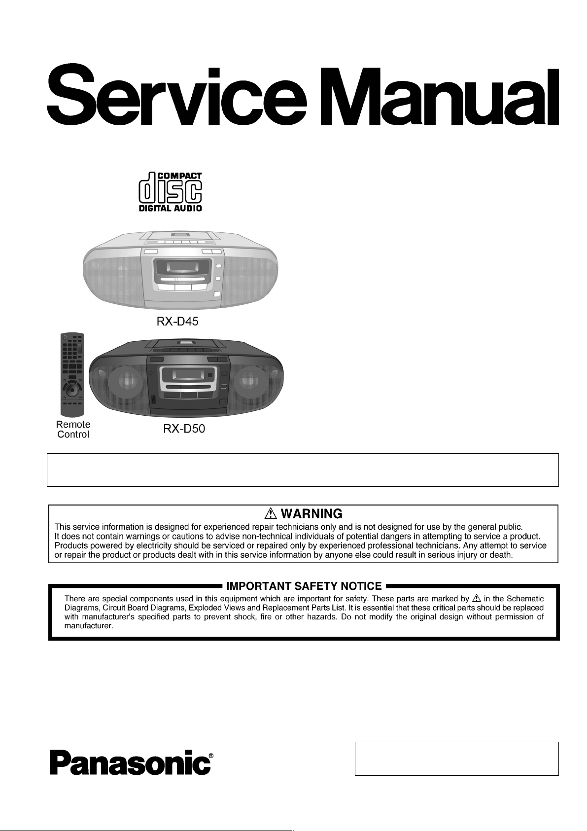
Portable Stereo CD System
Model No. RX-D45EB
RX-D45EG
RX-D50EB
RX-D50EG
Product Color : (W)...White Type (For RX-D45 only)
(S)...Silver Type (For RX-D50 only)
Notes: Please refer to the original service manual for:
G CD Mechanism Unit (DLS6F), Order No. PSG1002024AE
TABLE OF CONTENTS
PAGE PAGE
1 Safety Precautions ----------------------------------------------- 3
1.1. General Guidelines---------------------------------------- 3
1.2. Caution for AC Cord -------------------------------------- 4
1.3. Before Repair and Adjustment ------------------------- 5
1.4. Caution For Fuse Replacement ------------------------5
1.5. Protection Circuitry ----------------------------------------5
1.6. Safety Part Information ----------------------------------- 5
2 Warning --------------------------------------------------------------7
© Panasonic Corporation 2010. All rights reserved.
Unauthorized copying and distribution is a violation of
law.
Page 2

2.1. Prevention of Electro Static Discharge (ESD)
to Electrostatically Sensitive (ES) Devices ----------7
2.2. Precaution of Laser Diode -------------------------------8
2.3. Service caution based on Legal restrictions---------9
2.4. Handling Precaution for Traverse Unit-------------- 10
3 Service Navigation---------------------------------------------- 12
3.1. Service Information --------------------------------------12
4 Specifications ---------------------------------------------------- 13
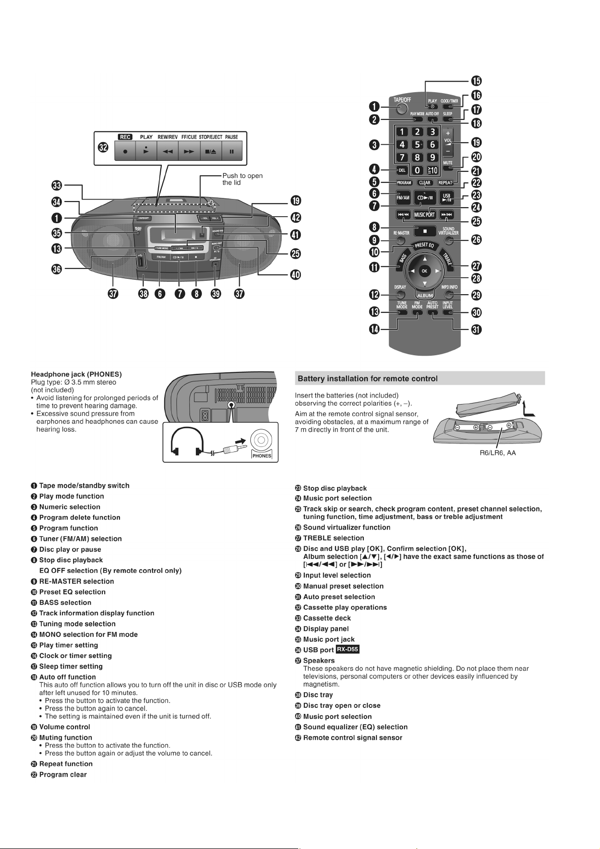
5 Location of Controls and Components------------------ 15
5.1. Main Unit Key Button Operations (RX-D45)------- 15
5.2. Main Unit and Remote Control Key Button
Operations (RX-D50)------------------------------------ 16
5.3. Disc Information ------------------------------------------ 17
6 Self Diagnostic and Doctor Mode Setting -------------- 18
6.1. Self Diagnostic Mode------------------------------------18
6.2. Doctor Mode (For RX-D45) ---------------------------19
6.3. Doctor Mode (For RX-D50) ---------------------------22
7 Service Fixture & Tools ---------------------------------------26
8 Disassembly and Assembly Instructions --------------- 27
8.1. Disassembly flow chart --------------------------------- 28
8.2. Main Parts Location Diagram -------------------------29
8.3. Disassembly of Top Cabinet Assembly------------- 30
8.4. Disassembly of Music Port (For RX-D50 only) --- 31
8.5. Disassembly of Front Panel Assembly -------------31
8.6. Disassembly of Panel P.C.B., Standby P.C.B.
and Volume P.C.B. ---------------------------------------32
8.7. Disassembly of Woofer Speaker (SP1)------------- 33
8.8. Disassembly of Woofer Speaker (SP2)------------- 34
8.9. Disassembly of CD Lid---------------------------------- 34
8.10. Disassembly of Deck Mechanism Unit ------------- 35
8.11. Disassembly of Deck P.C.B.--------------------------- 37
8.12. Disassembly of Cassette Lid -------------------------- 37
8.13. Disassembly of Mecha Bottom Cover -------------- 39
8.14. Disassembly of Power P.C.B. ------------------------- 40
8.15. Disassembly of Main P.C.B. --------------------------- 42
8.16. Replacement of Transisor (Q4107)------------------ 43
8.17. Replacement of Power IC (IC4101) ----------------- 45
8.18. Disassembly of CD Mechanism Unit ---------------- 47
8.19. Disassembly of CD Servo P.C.B.--------------------- 47
8.20. Disassembly of Battery (1) P.C.B.-------------------- 48
8.21. Disassembly of Battery (2) P.C.B.-------------------- 49
9 Disassembly and Assembly of Traverse Unit --------- 50
9.1. Disassembling Procedures ---------------------------- 50
9.2. Assembling Procedure---------------------------------- 51
10 Service Position ------------------------------------------------- 53
10.1. Checking & Repairing Deck P.C.B. ------------------ 53
10.2. Checking & Repairing Panel P.C.B. ----------------- 53
10.3. Checking & Repairing Power P.C.B. ---------------- 54
10.4. Checking & Repairing Main P.C.B. ------------------ 54
10.5. Checking & Repairing CD Servo P.C.B. ------------ 56
11 Measurements and Adjustments -------------------------- 57
11.1. Tuner Section --------------------------------------------- 57
11.2. Deck Mechanism Section ------------------------------ 59
12 Voltage Measurement & Waveform Chart--------------- 60
12.1. CD SERVO P.C.B. ---------------------------------------60
12.2. MAIN P.C.B. (1/2) ---------------------------------------- 61
12.3. MAIN P.C.B. (2/2) ---------------------------------------- 62
12.4. DECK P.C.B. ---------------------------------------------- 62
12.5. PANEL P.C.B. --------------------------------------------- 63
12.6. POWER P.C.B. ------------------------------------------- 63
12.7. Waveform Chart ------------------------------------------64
13 Illustration of IC’s, Transistors and Diodes------------ 65
14 Wiring Connection Diagram -------------------------------- 67
15 Schematic Diagram Notes----------------------------------- 69
16 Schematic Diagram -------------------------------------------- 71
16.1. CD SERVO CIRCUIT----------------------------------- 71
16.2. MAIN CIRCUIT (1/6)------------------------------------ 72
16.3. MAIN CIRCUIT (2/6)------------------------------------ 73
16.4. MAIN CIRCUIT (3/6)------------------------------------ 74
16.5. MAIN CIRCUIT (4/6)------------------------------------ 75
16.6. MAIN CIRCUIT (5/6)------------------------------------ 76
16.7. MAIN CIRCUIT (6/6)------------------------------------ 77
16.8. DECK CIRCUIT ------------------------------------------ 78
16.9. PANEL / VOLUME / STANDBY CIRCUIT --------- 79
16.10. POWER CIRCUIT --------------------------------------- 80
16.11. BATTERY (1) / BATTERY (2) / MUSIC PORT
CIRCUIT --------------------------------------------------- 81
17 Printed Circuit Board------------------------------------------ 82
17.1. CD SERVO / MUSIC PORT P.C.B. ----------------- 82
17.2. MAIN P.C.B.----------------------------------------------- 83
17.3. DECK / PANEL / VOLUME / STANDBY P.C.B. -- 84
17.4. POWER P.C.B. ------------------------------------------- 85
17.5. POWER / BATTERY (1) / BATTERY (2) P.C.B. -- 86
18 Terminal Function of IC’s ------------------------------------ 87
18.1. IC7001 (MN6627954AMA) IC SERVO
PROCESSOR -------------------------------------------- 87
18.2. IC7002 (BA5948FPE2) IC 4CH Drive -------------- 88
18.3. IC2100 (RFKWMD45EG-W) MICRO
PROCESSOR -------------------------------------------- 88
19 Exploded View and Replacement Parts List----------- 91
19.1. Exploded View and Mechanical replacement
Parts List--------------------------------------------------- 91
19.2. Electrical Replacement Parts List ------------------- 97
2
Page 3
1 Safety Precautions
1.1. General Guidelines
1. When servicing, observe the original lead dress. If a short circuit is found, replace all parts which have been overheated or
damaged by the short circuit.
2. After servicing, see to it that all the protective devices such as insulation barriers, insulation papers shields are properly
installed.
3. After servicing, carry out the following leakage current checks to prevent the customer from being exposed to shock hazards.
1.1.1. Leakage Current Cold Check
1. Unplug the AC cord and connect a jumper between the two prongs on the plug.
2. measure the resistance value, with an ohmmeter between the jumpered AC plug and each exposed metallic cabinet part on
the equipment such as screwheads, connectors, control shafts, etc. When the exposed metallic part has a return path to the
chassis, the reading should be between 1MΩ and 5.2MΩ. When the exposed metal does not have a return path to the chas-
sis, the reading must be
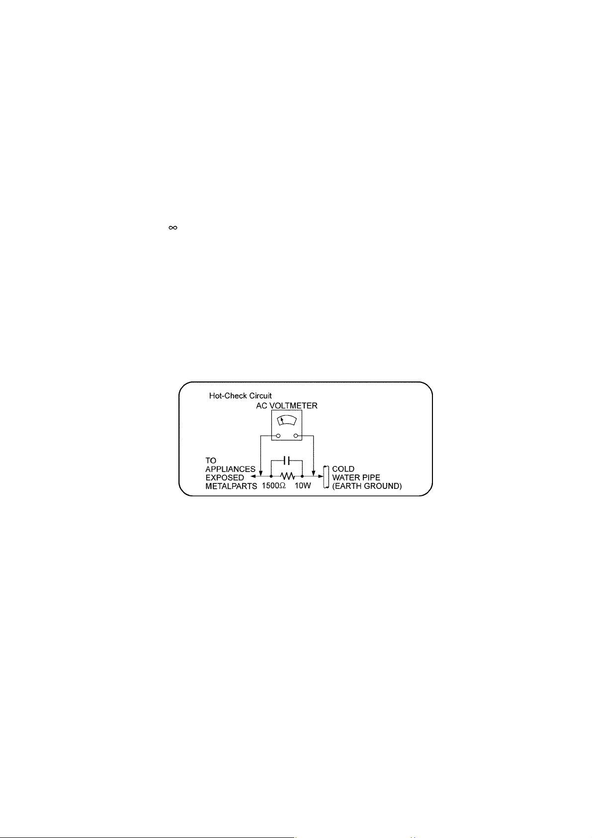
1.1.2. Leakage Current Hot Check
1. Plug the AC cord directly into the AC outlet. Do not use an isolation transformer for this check.
2. Connect a 1.5kΩ, 10 watts resistor, in parallel with a 0.15μF capacitors, between each exposed metallic part on the set and a
good earth ground such as a water pipe, as shown in Figure 1.
3. Use an AC voltmeter, with 1000 ohms/volt or more sensitivity, to measure the potential across the resistor.
4. Check each exposed metallic part, and measure the voltage at each point.
5. Reverse the AC plug in the AC outlet and repeat each of the above measurements.
6. The potential at any point should not exceed 0.75 volts RMS. A leakage current tester (Simpson Model 229 or equivalent)
may be used to make the hot checks, leakage current must not exceed 1/2 milliamp. In case a measurement is outside of the
limits specified, there is a possibility of a shock hazard, and the equipment should be repaired and rechecked before it is
returned to the customer.
Figure. 1
3
Page 4
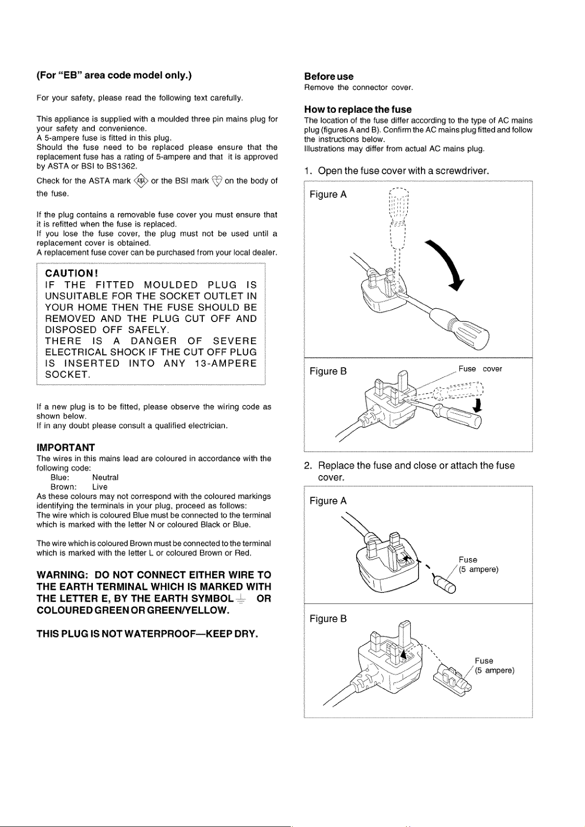
1.2. Caution for AC Cord
4
Page 5
1.3. Before Repair and Adjustment
Caution : DO NOT SHORT-CIRCUIT DIRECTLY (with a screwdriver blade, for instance), as this may destroy solid state devices.
After repairs are completed, restore power gradually using a variac, to avoid overcurrent.
• Current consumption at AC 230 V, 50Hz in TUNER VOL. MIN mode should be (~300 mA) respectively.
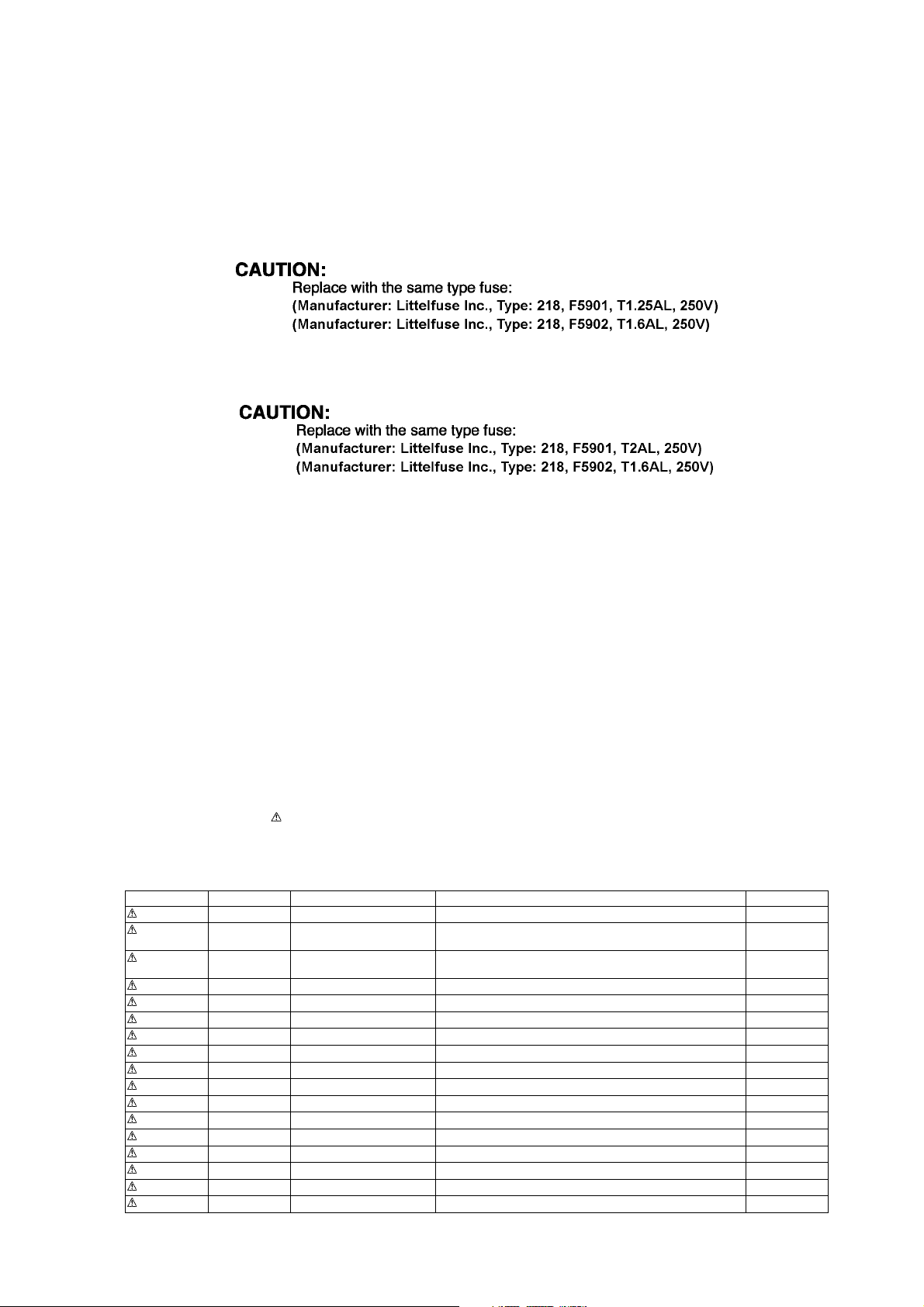
1.4. Caution For Fuse Replacement
1.4.1. For RX-D45
1.4.2. For RX-D50
1.5. Protection Circuitry
The protection circuitry may have operated if either of the following conditions are noticed:
• No sound is heard when the power is turned on.
• Sound stops during a performance.
The function of this circuitry is to prevent circuitry damage if, for example, the positive and negative speaker connection wires are
"shorted", or if speaker systems with an impedance less than the indicated rated impedance of the amplifier are used.
If this occurs, follow the procedure outlines below:
1. Turn off the power.
2. Determine the cause of the problem and correct it.
3. Turn on the power once again after one minute.
Note:
When the protection circuitry functions, the unit will not operate unless the power is first turned off and then on again.
1.6. Safety Part Information
Safety Parts List:
There are special components used in this equipment which are important for safety.
These parts are marked by in the Schematic Diagrams, Exploded View & Replacement Parts List. It is essential that these
critical parts should be replaced with manufacturer’s specified parts to prevent shock, fire or other hazards. Do not modify the
original design without permission of manufacturer.
Table 1
Safety Ref. No. Part No. Part Name & Description Remarks
401 RD-DAPX001-V TRAVERSE UNIT
A2 K2CZ3YY00005 AC CORD D50EB-S,
D45EB-W
A2 K2CQ2CA00007 AC CORD D50EG-S,
D45EG-W
A3 RQTX1035-E O/I BOOK (Du/Da/Sw) D50EG-S
A3 RQTX1034-D O/I BOOK (Ge/It/Fr) D50EG-S
A3 RQTX1041-Z O/I BOOK (En/Sp/Po/Cz) D50EG-S
A3 RQTX1148-B O/I BOOK (En) D50EB-S
A3 RQTX1031-D O/I BOOK (Ge/It/Fr) D45EG-W
A3 RQTX1032-E O/I BOOK (Du/Da/Sw) D45EG-W
A3 RQTX1040-Z O/I BOOK (En/Sp/Po/Cz) D45EG-W
A3 RQTX1147-B O/I BOOK (En) D45EB-W
PCB3 REPNT0063A POWER P.C.B. D45EB/EG-W
PCB3 REPNT0063B POWER P.C.B. D50EB/EG-S
T5902 G4C4BAH00003 TRANSFORMER D45EB/EG-W
T5903 G4C4BAH00002 BACK-UP TRANSFORMER D50EB/EG-S
T5904 G4C2AAH00002 TRANSFORMER
F5901 K5D122BLA014 FUSE D45EB/EG-W
5
Page 6

Safety Ref. No. Part No. Part Name & Description Remarks
F5901 K5D202BLA013 FUSE D50EB/EG-S
F5902 K5D162BLA013 FUSE
JK5901 K2AA2B000014 JK AC INLET
L5901 ELF15N035AN LINE FILTER
RL5901 K6B1AEA00003 RELAY
Z5902 ERZVA5Z471 ZNR
FP4100 K5G502A00039 FUSE PROTECTOR
FP5903 K5G502A00039 FUSE PROTECTOR
ZA5901 K3GE1ZZ00001 FUSE HOLDER
ZA5902 K3GE1ZZ00001 FUSE HOLDER
ZA5903 K3GE1ZZ00001 FUSE HOLDER
ZA5904 K3GE1ZZ00001 FUSE HOLDER
6
Page 7

2 Warning
2.1. Prevention of Electro Static Discharge (ESD) to Electrostatically Sensitive (ES) Devices
Some semiconductor (solid state) devices can be damaged easily by static electricity. Such components commonly are called Electrostatically Sensitive (ES) Devices. Examples of typical ES devices are integrated circuits and some field-effect transistors and
semiconductor “chip” components. The following techniques should be used to help reduce the incidence of component damage
caused by electrostatic discharge (ESD).
1. Immediately before handling any semiconductor component or semiconductor-equiped assembly, drain off any ESD on your
body by touching a known earth ground. Alternatively, obtain and wear a commercially available discharging ESD wrist strap,
which should be removed for potential shock reasons prior to applying power to the unit under test.
2. After removing an electrical assembly equiped with ES devices, place the assembly on a conductive surface such as aluminium foil, to prevent electrostatic charge build up or exposure of the assembly.
3. Use only a grounded-tip soldering iron to solder or unsolder ES devices.
4. Use only an anti-static solder remover device. Some solder removal devices not classified as “anti-static (ESD protected)” can
generate electrical charge sufficient to damage ES devices.
5. Do not use freon-propelled chemicals. These can generate electrical charges sufficient to damage ES devices.
6. Do not remove a replacement ES device from its protective package until immediately before you are ready to install it. (Most
replacement ES devices are packaged with leads electrically shorted together by conductive foam, aluminium foil or comparable conductive material).
7. Immediately before removing the protective material from the leads of a replacement ES device, touch the protective material
to the chassis or circuit assembly into which the device will be installed.
Caution :
Be sure no power is applied to the chassis or circuit, and observe all other safety precautions.
8. Minimize bodily motions when handling unpackaged replacement ES devices. (Otherwise harmless motion such as the
brushing together of your clothes fabric or the lifting of your foot from a carpeted floor can generate static electricity (ESD) suf-
ficient to damage an ES device).
7
Page 8
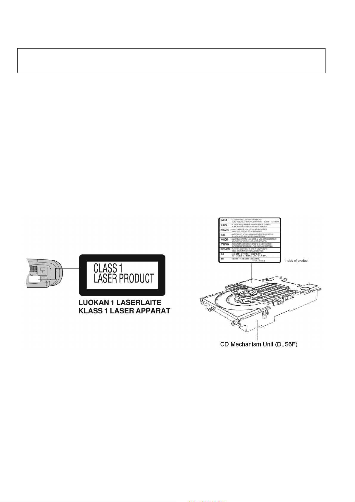
2.2. Precaution of Laser Diode
CAUTION!
THIS PRODUCT UTILIZES A LASER.
USE OF CONTROLS OR ADJUSTMENTS OR PERFORMANCE OF PROCEDURES OTHER THAN THOSE SPECIFIED HEREIN MAY RESULT
IN HAZARDOUS RADIATION EXPOSURE.
Caution:
This product utilizes a laser diode with the unit turned "on", invisible laser radiation is emitted from the pickup lens.
Wavelength: 795 nm (CD)
Maximum output radiation power from pickup: 100 μW/VDE
Laser radiation from the pickup unit is safety level, but be sure the followings:
1. Do not disassemble the pickup unit, since radiation from exposed laser diode is dangerous.
2. Do not adjust the variable resistor on the pickup unit. It was already adjusted.
3. Do not look at the focus lens using optical instruments.
4. Recommend not to look at pickup lens for a long time.
ACHTUNG :
Dieses Produkt enthält eine Laserdiode. Im eingeschalteten Zustand wird unsichtbare Laserstrahlung von der Lasereinheit
abgestrahlt.
Wellenlänge : 795 nm (CD)
Maximale Strahlungsleistung der Lasereinheit :100 μW/VDE
Die Strahlung an der Lasereinheit ist ungefährlich, wenn folgende Punkte beachtet werden:
1. Die Lasereinheit nicht zerlegen, da die Strahlung an der freigelegten Laserdiode gefährlich ist.
2. Den werkseitig justierten Einstellregler der Lasereinhit nicht verstellen.
3. Nicht mit optischen Instrumenten in die Fokussierlinse blicken.
4. Nicht über längere Zeit in die Fokussierlinse blicken.
8
Page 9

2.3. Service caution based on Legal restrictions
2.3.1. General description about Lead Free Solder (PbF)
The lead free solder has been used in the mounting process of all electrical components on the printed circuit boards used for this
equipment in considering the globally environmental conservation.
The normal solder is the alloy of tin (Sn) and lead (Pb). On the other hand, the lead free solder is the alloy mainly consists of tin
(Sn), silver (Ag) and Copper (Cu), and the melting point of the lead free solder is higher approx.30 degrees C (86°F) more than that
of the normal solder.
Definition of PCB Lead Free Solder being used
The letter of “PbF” is printed either foil side or components side on the PCB using the lead free solder.
(See right figure)
Service caution for repair work using Lead Free Solder (PbF)
• The lead free solder has to be used when repairing the equipment for which the lead free solder is used.
(Definition: The letter of “PbF” is printed on the PCB using the lead free solder.)
• To put lead free solder, it should be well molten and mixed with the original lead free solder.
• Remove the remaining lead free solder on the PCB cleanly for soldering of the new IC.
• Since the melting point of the lead free solder is higher than that of the normal lead solder, it takes the longer time to melt the
lead free solder.
• Use the soldering iron (more than 70W) equipped with the temperature control after setting the temperature at 350±30 degrees
C (662±86°F).
Recommended Lead Free Solder (Service Parts Route.)
• The following 3 types of lead free solder are available through the service parts route.
RFKZ03D01K-----------(0.3mm 100g Reel)
RFKZ06D01K-----------(0.6mm 100g Reel)
RFKZ10D01K-----------(1.0mm 100g Reel)
Note
* Ingredient: Tin (Sn), 96.5%, Silver (Ag) 3.0%, Copper (Cu) 0.5%, Cobalt (Co) / Germanium (Ge) 0.1 to 0.3%
9
Page 10
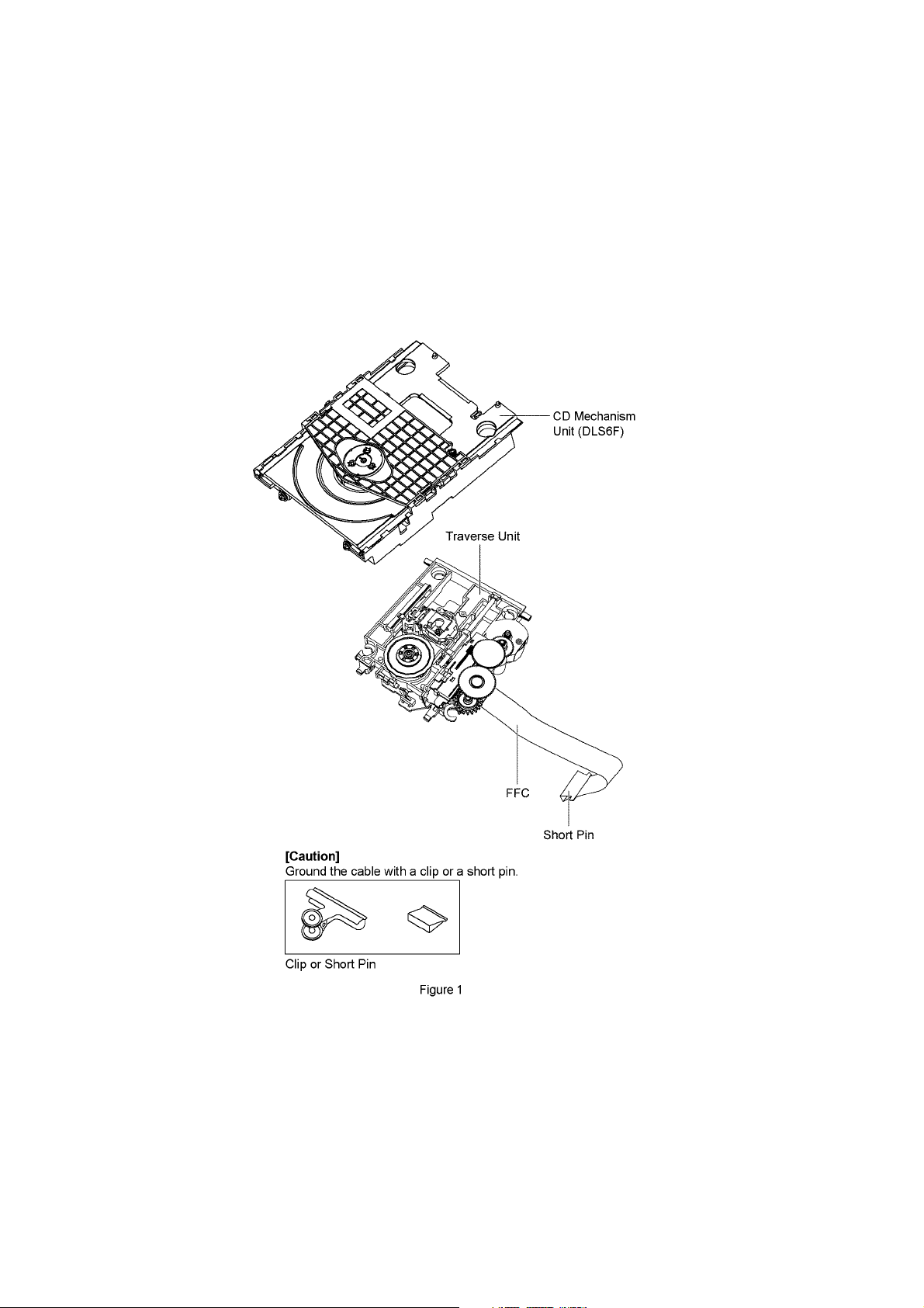
2.4. Handling Precaution for Traverse Unit
The laser diode in the optical pickup unit may break down due to static electricity of clothes or human body. Special care must be
taken avoid caution to electrostatic breakdown when servicing and handling the laser diode in the traverse unit.
2.4.1. Cautions to Be Taken in Handling the Optical Pickup Unit
The laser diode in the optical pickup unit may be damaged due to electrostatic discharge generating from clothes or human body.
Special care must be taken avoid caution to electrostatic discharge damage when servicing the laser diode.
1. Do not give a considerable shock to the optical pickup unit as it has an extremely high-precise structure.
2. To prevent the laser diode from the electrostatic discharge damage, the flexible cable of the optical pickup unit removed
should be short-circuited with a short pin or a clip.
3. The flexible cable may be cut off if an excessive force is applied to it. Use caution when handling the flexible cable.
4. The antistatic FPC is connected to the new optical pickup unit. After replacing the optical pickup unit and connecting the flexible cable, cut off the antistatic FPC.
2.4.2. Grounding for electrostatic breakdown prevention
Some devices such as the CD player use the optical pickup (laser diode) and the optical pickup will be damaged by static electricity
in the working environment. Proceed servicing works under the working environment where grounding works is completed.
2.4.2.1. Worktable grounding
1. Put a conductive material (sheet) or iron sheet on the area where the optical pickup is placed, and ground the sheet.
10
Page 11
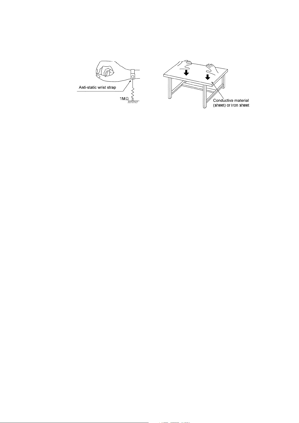
2.4.2.2. Human body grounding
1. Use the anti-static wrist strap to discharge the static electricity form your body (Figure 2).
Figure 2
11
Page 12

3 Service Navigation
3.1. Service Information
This service manual contains technical information which will allow service personnel’s to understand and service this model.
Please place orders using the parts list and not the drawing reference numbers.
If the circuit is changed or modified, this information will be followed by supplement service manual to be filed with original service
manual.
• CD Mechanism Unit (DLS6F):
1) This model uses CD Mechanism Unit (DLS6F).
• Micro-processor:
1) The following components are supplied as an assembled part.
• Micro-processor IC, (IC2100) is supplied as assembled part (RFKWMD45EG-W).
12
Page 13

4 Specifications
(RX-D45)
I Amplifier Section
RMS output power stereo mode
Front Ch (both channels
driven)
Total RMS stereo mode power 4 W
I FM/AM Tuner, Terminal Section
Preset station FM 16 stations
Frequency Modulation (FM)
Frequency range 87.50 MHz to 108.00 MHz (50 kHz
Amplitude Modulation (A M)
Frequency range 522 kHz to 1629 kHz (9 kHz step)
Headphone jack
Term in al Stereo, 3.5 mm jack (32 Ω)
I Disc Section
Disc played (8 cm or 12 cm) CD-Audio, CD-R/W (CD-DA)
Sampling frequency 44.1 kHz
Decoding 16 bit linear
Pick up
Wavelength 795 nm (CD)
Laser power CLASS 1 (CD)
Number of channels 2 channel, stereo
Wow and flutter Less than possible measurement
I Cassette Deck Section
Track system 4 track, 2 channel
Monitor system Variable sound monitor
Head
Record/playback Solid permalloy head
Motor DC servo motor
Recording system AC bias 84 kHz
Erase system Multi pole magnet
Tape speed 4.8 cm/s
Overall frequency response (+3 dB, -6 dB) at DECK OUT
NORMAL 50 Hz to 12 kHz
S/N ratio 50 dB (A weighted)
Wow and flutter 0.18% (WRMS)
Fast forward and rewind time Approx. 120 seconds with C-60 cas-
2 W per channel (8 Ω), 1 kHz, 10%
THD
AM 16 stations
step)
520 kHz to 1630 kHz (10 kHz step)
data
sette tape
Power consumption in standby mode: 0.8 W (approximate)
Notes :
1. Specifications are subject to change without notices.
Mass and dimensions are approximate.
2. Total harmonic distortion is measured by the digital spectrum analyzer.
(RX-D50)
I Amplifier Section
RMS output power stereo mode
Front Ch (both channels
driven)
Total RMS stereo mode power 6 W
I FM/AM Tuner, Terminal Section
Preset station FM 16 stations
Frequency Modulation (FM)
Frequency range 87.50 MHz to 108.00 MHz (50 kHz
Amplitude Modulation (AM)
Frequency range 522 kHz to 1629 kHz (9 kHz step)
Headphone jack
Terminal Stereo, 3.5 mm jack (32 Ω)
Music port (front) jack
Sensitivity 100 mV, 4.7 kΩ
Terminal Stereo, 3.5 mm jack
I Disc Section
Disc played (8 cm or 12 cm)
(1) CD-Audio (CD-DA)
(2) CD-R/RW (CD-DA, MP3* formatted disc)
(3) MP3*
* MPEG-1 Layer 3, MPEG-2 Layer 3
Bit rate
MP3 32 kbps to 320 kbps
Sampling frequency
CD 44.1 kHz
MP3 32 kHz, 44.1 kHz, 48 kHz
Decoding 16 bit linear
Pick up
Wavelength 795 nm (CD)
Laser power CLASS 1 (CD)
Number of channels 2 channel, stereo
Wow and flutter Less than possible measurement
3 W per channel (4 Ω), 1 kHz, 10%
THD
AM 16 stations
step)
520 kHz to 1630 kHz (10 kHz step)
data
I Speaker Section
Ty pe 1 way, 2 speaker system (Bass
reflex)
Speaker(S)
Full range 8 cm cone type
Impedance 8 Ω
I General
Power supply
AC 230 V, 50 Hz (EG)
230 V to 240 V, 50 Hz (EB)
Battery 12 V (8 x LR14, C)
Memory back-up 6 V (4 x R6/LR6, AA)
Power consumption 12 W (EG)
13 W (EB)
Dimensions (W x H x D) 408 mm x 148 mm x 255 mm
Mass 3.19 kg without batteries
Operating temperature range
Operating humidity range 35% to 80 % RH (no condensation)
0°C to +40°C
I Cassette Deck Section
Track system 4 track, 2 channel
Monitor system Variable sound monitor
Head
Record/playback Solid permalloy head
Motor DC servo motor
Recording system AC bias 84 kHz
Erase system Multi pole magnet
Tape speed 4.8 cm/s
Overall frequency response (+3 dB, -6 dB) at DECK OUT
NORMAL 50 Hz to 12 kHz
S/N ratio 50 dB (A weighted)
Wow and flutter 0.18% (WRMS)
Fast forward and rewind time Approx. 120 seconds with C-60 cas-
sette tape
I Speaker Section
Type 2 way, 2 speaker system (Bass
reflex)
13
Page 14

Speaker(S)
Full range 8 cm cone type
Tweeter 1.5 cm ceramic tweeter type
Impedance 4 Ω
I General
Power supply
AC 230 V, 50 Hz
Battery 12 V (8 x LR14, C)
Memory back-up 6 V (4 x R6/LR6, AA)
Power consumption 14 W
Dimensions (W x H x D) 408 mm x 148 mm x 255 mm
Mass 3.28 kg without batteries
Operating temperature range 0°C to +40°C
Operating humidity range 35% to 80 % RH (no condensation)
Power consumption in standby mode: 0.8 W (approximate)
Notes :
1. Specifications are subject to change without notices.
Mass and dimensions are approximate.
2. Total harmonic distortion is measured by the digital spectrum analyzer.
14
Page 15
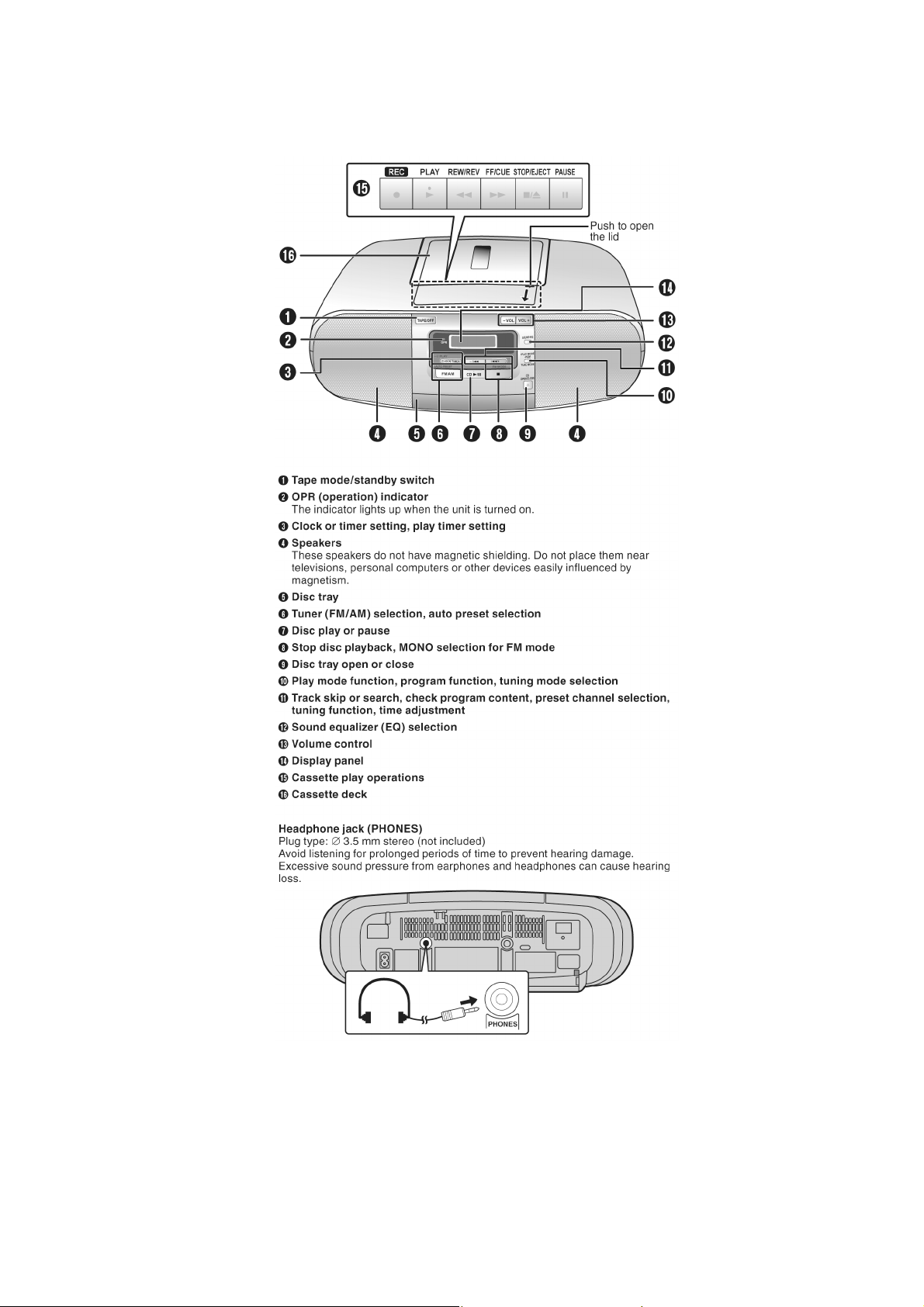
5 Location of Controls and Components
5.1. Main Unit Key Button Operations (RX-D45)
15
Page 16
5.2. Main Unit and Remote Control Key Button Operations (RX-D50)
16
Page 17
5.3. Disc Information
5.3.1. Disc Information (RX-D45)
5.3.2. Disc Information (RX-D50)
17
Page 18
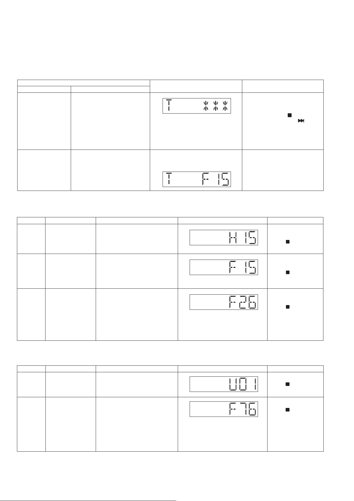
6 Self Diagnostic and Doctor Mode Setting
This unit is equiped with features of self diagnostic & doctor mode setting for checking the functions & reliability.
6.1. Self Diagnostic Mode
6.1.1. Self Diagnostic Table
Item FL display Key operation
Mode name Description
Self Diagnostic Mode To enter into self diagnostic
checking
1. Select CD mode
(Ensure no CD inserted).
㪁㩷㪁㩷㪁㩷䋺㩷㪜㫉㫉㫆㫉㩷㪺㫆㪻㪼
Error code information Error code will display
System will perform a check on
any unusual/error code from the
memory
Example:
6.1.2. Self Diagnostic Error Code 1 (For CD)
Error Code
H15 CD Open SW
F15 CD REST SW
Diagnostic Contents Description of error
Abnormal
Abnormal
During normal operation CD OPEN
SW On fail to be detected with 4
sec. Error No. shall be clear by
force or during cold start.
CD traverse position intial setting
operation failsafe counter (1000
ms) waiting for REST SW to turn
on. Error No. shall be clear by
force or during cold start.
FL display
2. Press and hold [ ] for
2 seconds follow by [ /+] on
main unit.
To exit, press [TAPE/OFF] on
main uint.
1. In self diagnosis mode.
2. Press [STOP] for on main unit.
To exit, press [TAPE/OFF] on
main uint.
Remarks
For CD Mechanism Unit
(DLS6F) (For Traverse).
Press [ ] on main unit
for next error
For CD Mechanism Unit
(DLS6F) (For Traverse).
Press [ ] on main unit
for next error
F26 Communication
between CD servo
LSI and micro-p
abnormal.
CD function DTMS command, after
system setting, If SENSE = 'L'
cannot be detected. Memory shall
contain F26 code. After Power on,
CD function shall continue, error
display shall be "NO DISC".
Error No. shall be clear by force or
cold start.
6.1.3. Self Diagnostic Error Code 2 (For Power Supply)
Error Code
U01 Battery Low Detect the Battery when Battery is
F76 Abnormality in the
Diagnostic Contents Description of error
Low.
output voltage of
stabilized power
supply
In normal operation when DCDET1
is detected "L" (Low) for two
consecutive times, F76 is
displayed on FL for 1 second and
after that PCONT will be turned to
"L" (Low). This is due to any of the
DC voltages (+9V, +7V, -7V, +5V,
+5.3V etc.) not available.
FL display
For CD Mechanism Unit
(DLS6F) (For Traverse).
Press [ ] on main unit
for next error
Remarks
For Power.
Press [ ] on main unit
for next error
For Power.
Press [ ] on main unit
for next error
18
Page 19
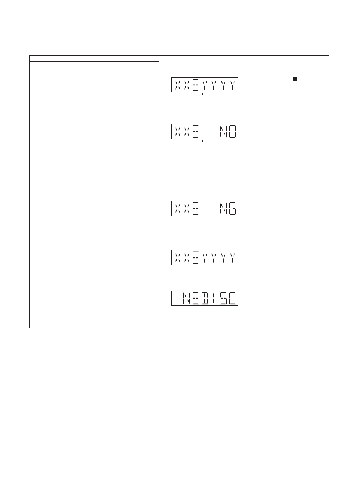
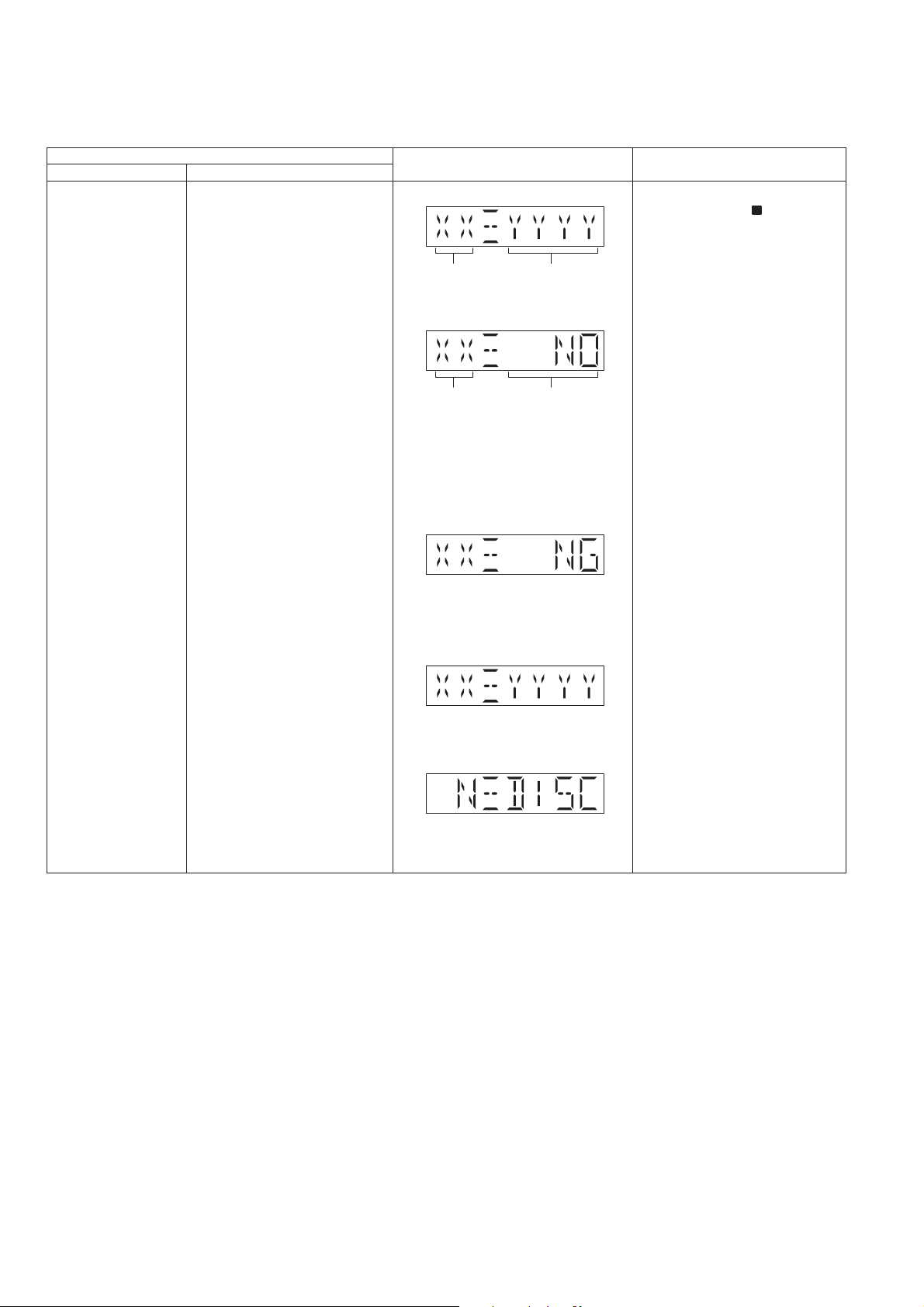
6.2. Doctor Mode (For RX-D45)
6.2.1. Doctor Mode Table 1
Item FL display Key operation
Mode name Description
Doctor Mode In any mode:
To enter into Doctor Mode for
checking of various items and
displaying EEPROM and firmware
version.
Note: The micro-processor
version as shown is an example.
It will be revise when there is an
updates.
FL Display sequence
Display 1 > 2
Version Display
(Display 1)
(DEC)
Checksum : (Condition 1)
Checksum
(HEX)
1. Press and hold [ ] on main unit
follow by [-VOL] on main unit.
To exit, press [TAPE/OFF] on
main uint.
Version Display
(DEC)
(a) If there is NO EEPROM header
string OR
(b) If there is no EEPROM ( no data is
received by micro-processor) [NO] is
displayed.
Checksum : (Condition 2)
If the version of the EEPROM does not
match or not working properly [NG] is
display.
Checksum : (Condition 3)
If the EEPROM version matches,
checksum [YYYY] is displayed.
The Checksum of EEPROM and
firmware version will be display for 2
sec.
Check sum
(HEX)
(Display 2)
19
Page 20
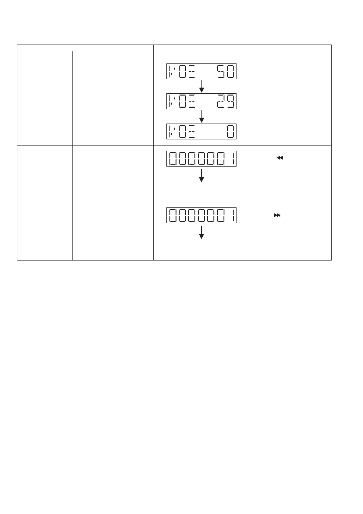
6.2.2. Doctor Mode Table 2
Item FL display Key operation
Mode name Description
Volume Setting In Doctor Mode:
To check for volume setting during
this mode, Bass & treble is set to
0dB & EQ is switch off.
Display for 1 sec
Display for 1 sec
1. Select to FM mode and Press
[SOUND EQ] on main unit.
To exit, press [TAPE/OFF] on
main uint.
CD Loading Test Mode
(DLS6F)
CD Combination Test
Mode (DLS6F)
To determine the reliability of CD
Loading unit.
To check for the Open/Close
operation for the CD loading unit.
It fails when there is abnormality
in opening or closing.
A combination of CD loading &
traverse unit test.
The counter will increment by one.
When reach 9999999 will change to
0000000
The counter will increment by one.
When reach 9999999 will change to
0000000
In Doctor Mode:
1. Press [-/ ] on main unit.
To exit, press [TAPE/OFF] on
main uint.
(Refer to section 6.2.3. for more
information).
In Doctor Mode:
1. Press [ /+] on main unit.
To exit, press [TAPE/OFF] on
main uint.
(Refer to section 6.2.4. for more
information).
20
Page 21
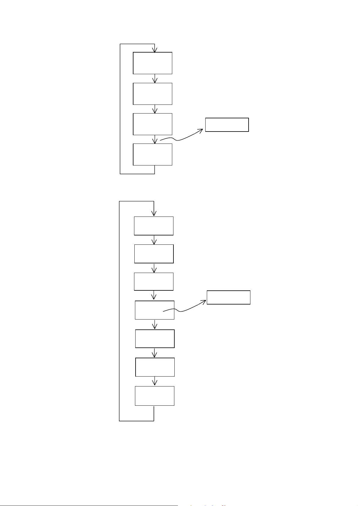
6.2.3. CD Loading Test Mode
OPEN
Operation
OPEN wait
for 1 s
CLOSE
Operation
CLOSE
wait for 4s
6.2.4. CD Combination Test Mode
First Track
Access
First Track
Play 10 s
Last Track
Access
Count Up
Last Track
Play 10 s
OPEN
Operation
OPEN wait
for 1 s
CLOSE
Operation
Count Up
21
Page 22
6.3. Doctor Mode (For RX-D50)
6.3.1. Doctor Mode Table 1
Item FL display Key operation
Mode name Description
Doctor Mode In any mode:
To enter into Doctor Mode for
checking of various items and
displaying EEPROM and firmware
version.
(Display 1)
1. Press and hold [ ] on main
unit follow by [4] and [7] on
remote control.
Note: The micro-processor
version as shown is an example.
It will be revise when there is an
updates.
FL Display sequence
Display 1 > 2
Version Display
(DEC)
Checksum : (Condition 1)
Version Display
(DEC)
(a) If there is NO EEPROM header
string OR
(b) If there is no EEPROM ( no data is
received by micro-processor) [NO] is
displayed.
Checksum : (Condition 2)
If the version of the EEPROM does not
match or not working properly [NG] is
display.
Checksum : (Condition 3)
Checksum
(HEX)
Check sum
(HEX)
To exit, press [TAPE/OFF] on
main uint.
If the EEPROM version matches,
checksum [YYYY] is displayed.
(Display 2)
The Checksum of EEPROM and
firmware version will be display for 2
sec.
22
Page 23
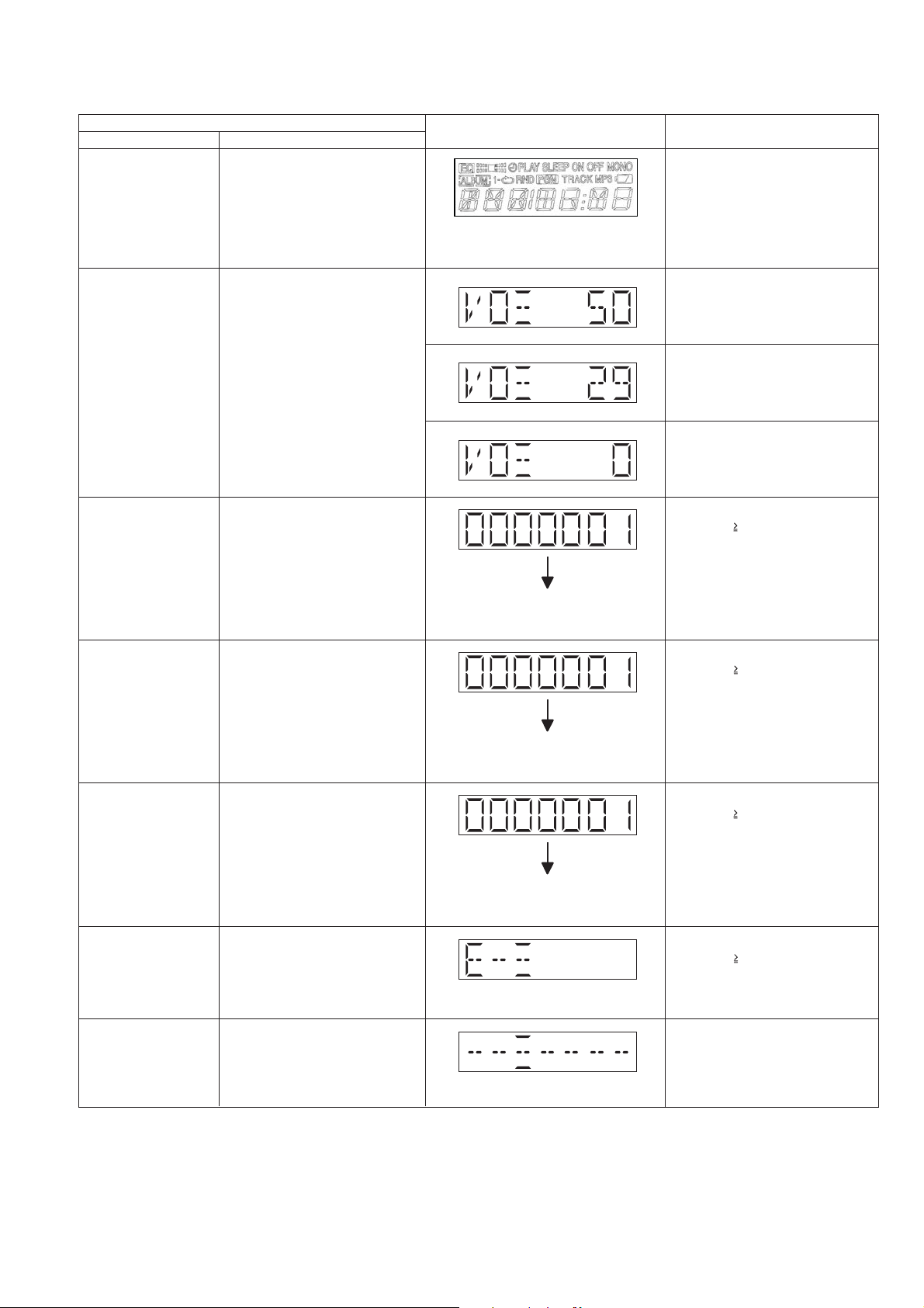
6.3.2. Doctor Mode Table 2
Item FL display Key operation
Mode name Description
FL Display Test In Doctor Mode:
To check the FL segments display
(All segments will light up)
1. Press [AUTO OFF] on remote
control.
To cancel, press [0] on remote
control.
To exit, press [TAPE/OFF] on main
uint.
Volume Setting In Doctor Mode:
To check for volume setting during
this mode, Bass & treble is set to
0dB & EQ is switch off.
1. Press [7] on remote control.
To exit, press [TAPE/OFF] on main
uint.
In Doctor Mode:
1. Press [8] on remote control.
To exit, press [TAPE/OFF] on main
uint.
In Doctor Mode:
1. Press [9] on remote control.
To exit, press [TAPE/OFF] on main
uint.
CD Loading Test Mode
(DLS6F)
CD Traverse Unit Test
Mode (DLS6F)
To determine the reliability of CD
Loading unit.
To check for the Open/Close
operation for the CD loading unit.
It fails when there is abnormality
in opening or closing.
To check for the traverse unit
operation. In this mode, the first &
last track is access & read. (TOC).
It fails when TOC is not completed
by IOS or the traverse is out of
focus.
The counter will increment by one.
When reach 9999999 will change to
0000000
The counter will increment by one.
When reach 9999999 will change to
0000000
In Doctor Mode:
1. Press [ 10], [1], [1] on remote
control.
To exit, press [TAPE/OFF] on main
uint.
(Refer to section 6.3.3. for more
information).
In Doctor Mode:
1. Press [ 10], [1], [2] on remote
control.
To exit, press [TAPE/OFF] on main
uint.
(Refer to section 6.3.4. for more
information).
CD Combination Test
Mode (DLS6F)
CD Self-Adjustment
(AJST) Result Display
Cold Start In Doctor Mode:
A combination of CD loading &
traverse unit test.
The following shall be displayed
for 2.5 secs. The result shall
correspond to the condition met
as shown.
To activate cold start upon next
AC power up.
The counter will increment by one.
When reach 9999999 will change to
0000000
Display of auto adjustment result
In Doctor Mode:
1. Press [ 10], [1], [3] on remote
control.
To exit, press [TAPE/OFF] on main
uint.
(Refer to section 6.3.5. for more
information).
In Doctor Mode:
1. Press [ 10], [1], [4] on remote
control.
To exit, press [TAPE/OFF] on main
uint.
1. Press [SLEEP] on remote
control.
To exit, press [TAPE/OFF] on main
uint.
23
Page 24
6.3.3. CD Loading Test Mode
OPEN
Operation
OPEN wait
for 1 s
6.3.4. CD Traverse Unit Test
CLOSE
Operation
CLOSE
wait for 4s
First Track
Access
First Track
Play 5 s
Last Track
Access
Count Up
Last Track
Play 5 s
Count Up
24
Page 25
6.3.5. CD Combination Test Mode
First Track
Access
First Track
Play 10 s
Last Track
Access
Last Track
Play 10 s
Operation
Count Up
OPEN
OPEN wait
for 1 s
CLOSE
Operation
25
Page 26

7 Service Fixture & Tools
Prepare service tools before proccess service position.
Service Tools Remarks
Deck P.C.B. (JW830) - Main P.C.B. (CN2104) REXN0084 (10P cable)
Panel P.C.B. (ZJ903) - Main P.C.B. (CN4104) REXN0082 (4P cable)
Panel P.C.B. (CN900) - Main P.C.B. (CN2105) REXN0080 (10P cable)
26
Page 27
8 Disassembly and Assembly Instructions
Caution Note:
• This section describes the disassembly and/or assembly procedures for all major printed circuit boards & main components for the unit. (You may refer to the section of “Main components and P.C.B Locations” as described in the service
manual)
• Before carrying out the disassembly process, please ensure all the safety precautions & procedures are followed.
• During the disassembly and/or assembly process, please handle with care as there may be chassis components with
sharp edges.
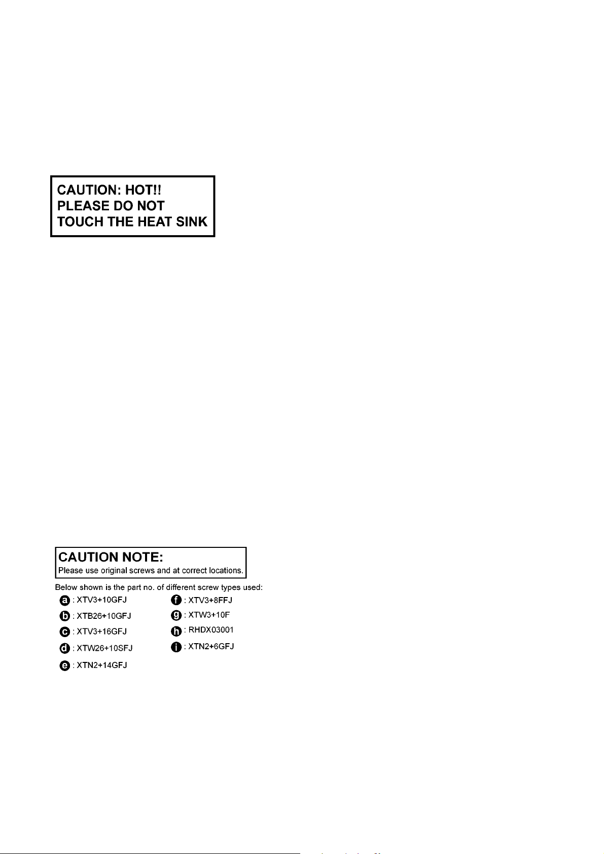
• Avoid touching heatsinks due to its high temperature after prolong use. (See caution as described below)
• During disassembly and assembly, please ensure proper service tools, equipments or jigs is being used.
• During replacement of component parts, please refer to the section of “Replacement Parts List” as described in the
service manual.
• Select items from the following indexes when disassembly or replacement are required.
• Disassembly of Top Cabinet Assembly
• Disassembly of Music Port P.C.B. (for RX-D50 only)
• Disassembly of Front Panel Assembly
• Disassembly of Panel P.C.B., Standby P.C.B. and Volume P.C.B.
• Disassembly of Woofer Speaker (SP1)
• Disassembly of Woofer Speaker (SP2)
• Disassembly of CD Lid
• Disassembly of Deck Mechanism Unit
• Disassembly of Deck P.C.B.
• Disassembly of Cassette Lid
• Disassembly of Mecha Bottom Cover
• Disassembly of Power P.C.B.
• Disassembly of Main P.C.B.
• Replacement of Transistor (Q4107)
• Replacement of Power IC (IC4101)
• Disassembly of CD Mechanism Unit
• Disassembly of CD Servo P.C.B.
• Disassembly of Battery (1) P.C.B.
• Disassembly of Battery (2) P.C.B.
27
Page 28

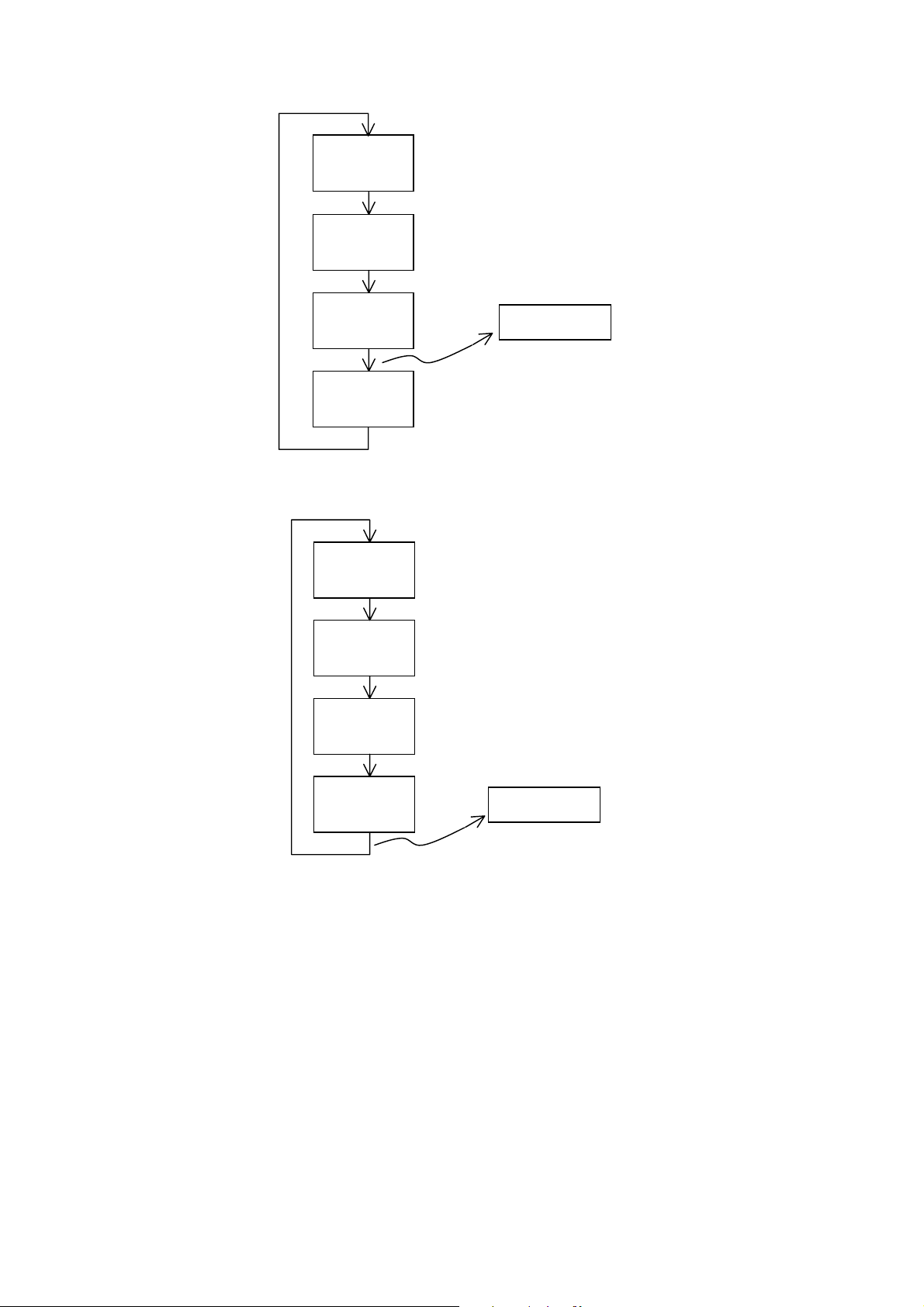
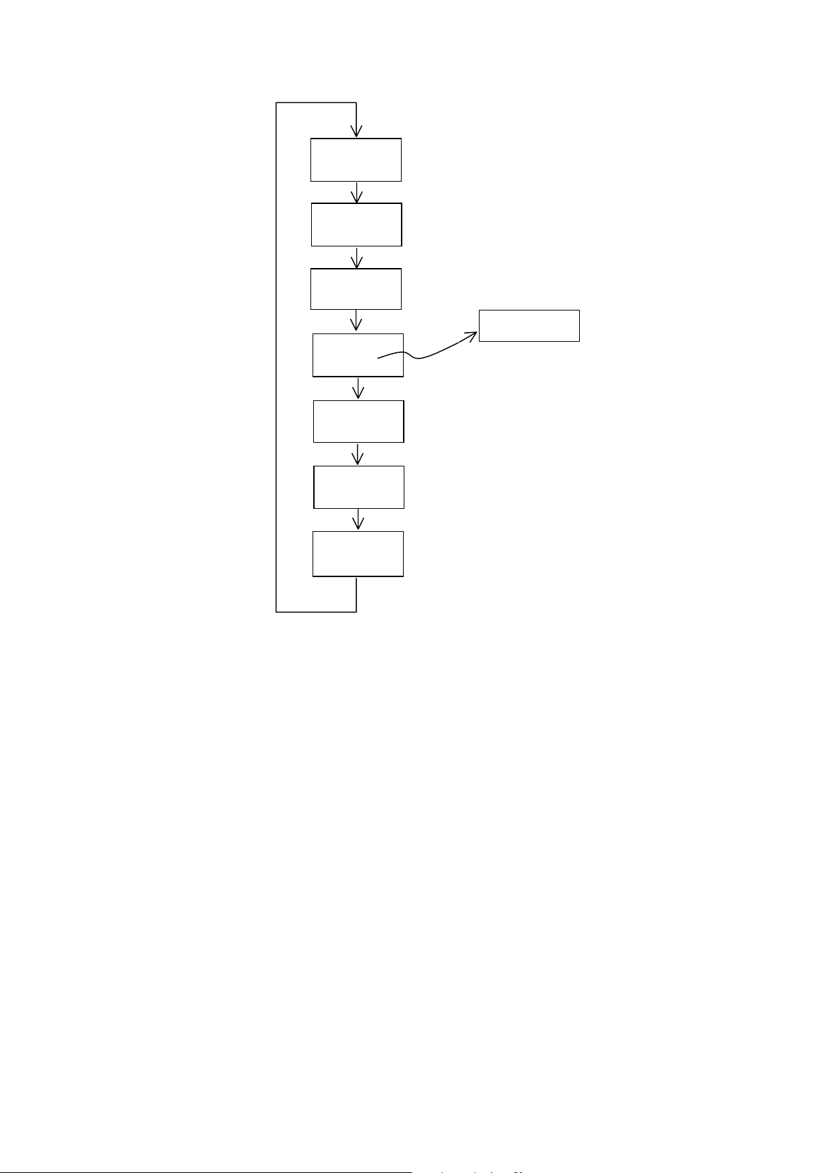
8.1. Disassembly flow chart
The following chart is the procedure for disassembling the casing and inside parts for internal inspection when carrying out the servicing.
To assemble the unit, reverse the steps shown in the chart below.
28
Page 29
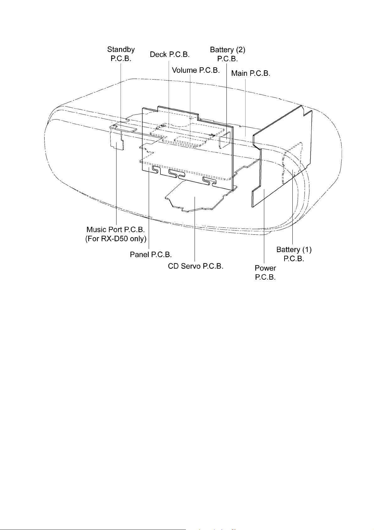
8.2. Main Parts Location Diagram
29
Page 30
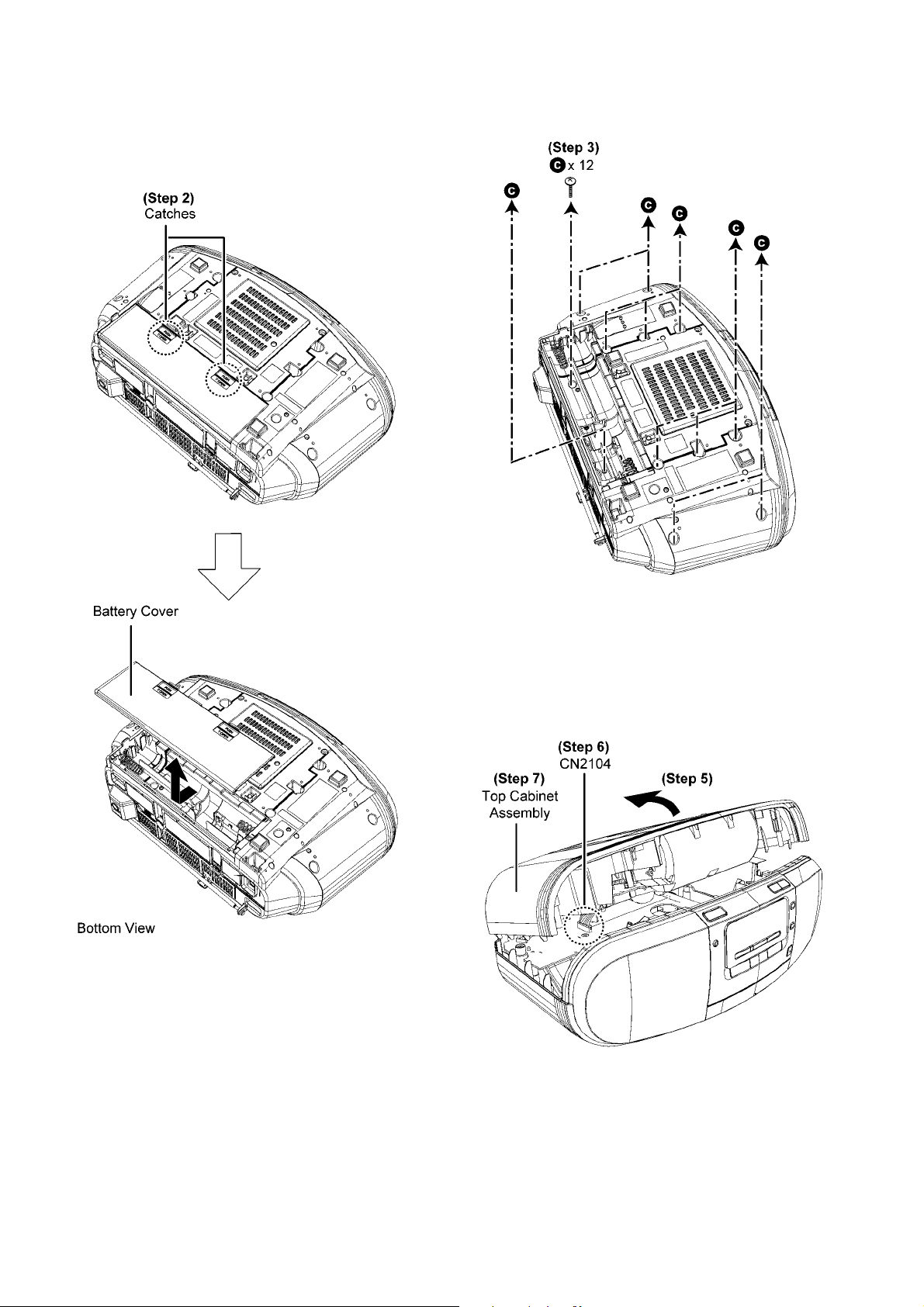
8.3. Disassembly of Top Cabinet Assembly
Step 1 : Upset the unit.
Step 2 : Release 2 catches to remove Battery Cover.
Step 3 : Remove 12 screws.
Step 4 : Upset the unit.
Step 5 : Slightly lift up the Top Cabinet Assembly as arrow
shown.
Step 6 : Detach 10P cable at the connector (CN2104) on Main
P.C.B..
Step 7 : Remove the Top Cabinet Assembly.
30
Page 31

8.4. Disassembly of Music Port (For
8.5. Disassembly of Front Panel
RX-D50 only)
• Refer to “Disassembly of Top Cabinet Assembly”.
Step 1 : Remove 2 screws.
Step 2 : Lift up the Standby P.C.B..
Assembly
• Refer to “Disassembly of Top Cabinet Assembly”.
Step 1 : Upset the unit.
Step 2 : Remove 2 screws.
Step 3 : Detach 3P cable at the connector (CN4105) on Main
P.C.B..
Step 4 : Remove 1 screw.
Step 5 : Remove the Music Port P.C.B..
Step 3 : Detach 4P cable at the connector (CN4104) on Main
P.C.B..
Step 4 : Detach 10P cable at the connector (CN2105) on Main
P.C.B..
Step 5 : Detach 3P cable at the connector (CN4105) on Main
P.C.B. (For RX-D50 only).
31
Page 32

Step 6 : Remove Front Panel Assembly as arrow shown.
Caution : During assembling, ensure the Front Panel
Assembly properly fixed to the Main P.C.B..
8.6. Disassembly of Panel P.C.B., Standby P.C.B. and Volume P.C.B.
• Refer to “Disassembly of Top Cabinet Assembly”.
• Refer to “Disassembly of Front Panel Assembly”.
Step 1 : Remove 4 screws.
Step 2 : Lift up the Volume P.C.B. and Standby P.C.B..
Step 3 : Remove 4 screws.
Caution : During assembling, ensure the Panel P.C.B. is
properly into the Locator.
32
Page 33

Step 4 : Desolder 2P wire at (ZJ901) on the Panel P.C.B..
Step 5 : Desolder 2P wire at (ZJ902) on the Panel P.C.B..
8.7. Disassembly of Woofer Speaker (SP1)
• Refer to “Disassembly of Top Cabinet Assembly”.
• Refer to “Disassembly of Front Panel Assembly”.
Step 1 : Desolder 2P wire on Woofer Speaker (SP1).
Step 2 : Remove 4 screws.
Step 3 : Remove Woofer Speaker (SP1).
Step 6 : Release both 2P wires (ZJ901 and ZJ902) from
the slot of the Panel P.C.B..
Step 7 : Remove the Panel P.C.B., Volume P.C.B. and Standby
P.C.B. altogether.
33
Page 34

8.8. Disassembly of Woofer Speaker (SP2)
• Refer to “Disassembly of Top Cabinet Assembly”.
• Refer to “Disassembly of Front Panel Assembly”.
Step 1 : Desolder 2P wire on Woofer Speaker (SP2).
Step 2 : Remove 4 screws.
Step 3 : Remove Woofer Speaker (SP2).
8.9. Disassembly of CD Lid
• Refer to “Disassembly of Top Cabinet Assembly”.
• Refer to “Disassembly of Front Panel Assembly”.
Step 1 : Remove the Spring as arrow shown in order of
sequences (1) to (3).
Caution : Keep the spring in the safe place and place them
back during assembling.
Step 2 : Push shafts of CD Lid inward as arrows shown.
34
Page 35

Step 3 : Remove the CD Lid.
8.10. Disassembly of Deck Mechanism Unit
• Refer to “Disassembly of Top Cabinet Assembly”.
Step 1 : Remove 3 screws.
Step 2 : Open Mecha Bottom Cover as arrow shown.
Step 3 : Press the STOP/EJECT button to open Cassette Lid.
35
Page 36

Step 4 : Remove the Deck Mechanism Unit as arrow shown.
Caution : During assembling, ensure the Deck Mechanism
Unit is properly sitted under the Catch.
Caution : During assembling, ensure the Deck Mechanism
Unit is properly fitted into the Locator.
36
Page 37

8.11. Disassembly of Deck P.C.B.
• Refer to “Disassembly of Top Cabinet Assembly”.
Step 1 : Remove 2 screws.
Step 2 : Desolder 2P wire at (JW501) on the Deck P.C.B..
8.12. Disassembly of Cassette Lid
• Refer to “Disassembly of Top Cabinet Assembly”.
• Refer to “Disassembly of Deck Mechanism Unit”.
Step 1 : Release 1 catch.
Step 3 : Detach 4P wire at the connector (CP303) on Deck
P.C.B..
Step 4 : Remove the Deck P.C.B..
Step 2 : Remove the Dumper Gear as arrow shown.
37
Page 38

Step 3 : Lift up the Spring as arrow shown.
Step 4 : Remove the Spring.
Step 6 : Remove Cassette Lid as arrow shown.
Step 5 : Push the shafts of Cassette Lid inward as arrow
shown.
38
Page 39

8.13. Disassembly of Mecha Bottom Cover
• Refer to “Disassembly of Top Cabinet Assembly”.
Step 1 : Remove 3 screws.
Step 2 : Remove the Top Cover.
Step 4 : Open the Mecha Bottom Cover as arrow shown.
Step 5 : Using flat screwdriver slightly push the shaft (A) of
Mecha Bottom Cover in order of sequence (1) to (2) as arrow
shown.
Step 3 : Release the Spring as arrow shown.
39
Page 40

Step 6 : Using flat screwdriver slightly push the shaft (B) of
Mecha Bottom Cover in order of sequence (3) to (4) as arrow
shown.
8.14. Disassembly of Power P.C.B.
• Refer to “Disassembly of Top Cabinet Assembly”.
Step 1 : Remove 1 screw.
Step 7 : Remove the Mecha Bottom Cover as arrow shown.
Step 2 : Lift and remove the PCB Support as arrow shown.
Caution : During assembling, ensure the PCB Support is
seated properly on the Locator.
40
Page 41

Step 3 : Remove 4 screws.
Step 4 : Detach 8P cable at the connector (CN4100) on Main
P.C.B..
Step 5 : Remove the cables from the slot.
Caution : During assembling, ensure the cables as prop-
erly inserted into the Slot.
Step 6 : Lift up the Power P.C.B. as arrow shown.
41
Page 42

Step 7 : Release 6 catches.
Step 8 : Remove the Safety cover.
8.15. Disassembly of Main P.C.B.
• Refer to “Disassembly of Top Cabinet Assembly”.
Step 1 : Detach 4P cable at the connector (CN4104) on Main
P.C.B..
Step 2 : Detach 10P cable at the connector (CN2105) on Main
P.C.B..
Step 3 : Detach 3P cable at the connector (CN4105) on Main
P.C.B. (For RX-D50 only).
Step 9 : Desolder 4P cable at (JW920) on the Power P.C.B..
Step 10 : Remove Power P.C.B..
Step 4 : Detach 22P FFC at the connector (CN2101) on Main
P.C.B..
Step 5 : Detach 8P cable at the connector (CN4100) on Main
P.C.B..
Step 6 : Remove 3 screws.
42
Page 43

Step 7 : Lift up to remove Main P.C.B..
Caution 1 : During assembling, ensure the Main P.C.B. is
seated properly on the Locator.
Caution 2 : During assembling, ensure the Main P.C.B. is
slot into the Front Panel Assembly.
8.16. Replacement of Transisor (Q4107)
• Refer to “Disassembly of Main P.C.B.”
8.16.1. Disassembly of Transistor (Q4107)
Step 1 : Desolder pins of the Transistor (Q4107) on the solder
side of Main P.C.B..
Step 2 : Remove 1 screw.
43
Page 44

Step 3 : Remove the Transistor (Q4107).
Caution : Avoid touching the Heatsink Unit due to its high
temperature after prolonged use. Touching it may lead to
injuries.
Step 3 : Fix 1 screw on the Transistor (Q4107) onto the Heat-
sink Unit.
Step 4 : Solder pins of the Transistor (Q4107) on the solder
side of Main P.C.B..
Caution : Check for the solderability of the Transistor
(Q4107).
8.16.2. Assembly of Transistor (Q4107)
Step 1 : Apply Grease to the Heatsink Unit.
Step 2 : Install the Transistor (Q4107) on Main P.C.B. as arrow
shown.
Caution : Ensure the pins are inserted and seated properly
on Main P.C.B..
44
Page 45

8.17. Replacement of Power IC (IC4101)
• Refer to “Disassembly of Main P.C.B.”
8.17.1. Disassembly of Power IC (IC4101)
Step 1 : Desolder pins of the Heatsink Unit.
Step 4 : Desolder pins of the Power IC (IC4101) on the solder
side of the Main P.C.B..
Step 5 : Remove the Power IC (IC4101).
Step 2 : Remove 1 screw.
Step 3 : Remove Heatsink Unit.
Caution : Avoid touching the Heatsink Unit due to its high
temperature after prolonged use. Touching it may lead to
injuries.
45
Page 46

8.17.2. Assembly of Power IC (IC4101)
Step 1 : Install the Power (IC4101) on Main P.C.B..
Caution : Ensure the pins are inserted and seated properly
on Main P.C.B..
Step 2 : Solder pins of the Power IC (IC4101) on the solder
side of Main P.C.B..
Step 3 : Apply Grease to the Heatsink Unit.
Step 4 : Install the Heatsink Unit on Main P.C.B.
Caution : Ensure the pins are inserted and seated properly
on Main P.C.B..
Step 5 : Fix 1 screw on the Transsistor (Q4107) onto the Heat-
sink Unit.
Caution : Check the solderability of the Transistor (Q4107)
and Power IC (IC4101).
Step 5 : Solder pins of the Heatsink Unit on the solder side of
Main P.C.B..
46
Page 47

8.18. Disassembly of CD Mecha-
8.19. Disassembly of CD Servo
nism Unit
• Refer to “Disassembly of Top Cabinet Assembly”.
• Refer to “Disassembly of Main P.C.B.”
Step 1 : Remove 2 screws.
Step 2 : Remove CD Mechanism Unit as arrow shown.
P.C.B.
• Refer to “Disassembly of CD Mechanism Unit”
Step 1 : Remove 3 screws.
Step 2 : Desolder pins of the Traverse Motor Unit.
Step 3 : Lift up the CD Servo P.C.B. and turn it over.
Step 4 : Detach 16P FPC at the connector (CN7001) on the CD
Servo P.C.B..
Step 5 : Remove the CD Servo P.C.B..
47
Page 48

8.20. Disassembly of Battery (1) P.C.B.
• Refer to “Disassembly of Top Cabinet Assembly”.
• Refer to “Disassembly of Main P.C.B.”
Step 1 : Release the catch.
Step 2 : Remove the Battery (1) P.C.B. as arrow shown.
Step 3 : Desolder 4P cable at (CN921) on the Battery (1)
P. C. B.
Caution : During assembling, ensure the cable is properly
inserted into the slot.
48
Page 49

8.21. Disassembly of Battery (2) P.C.B.
• Refer to “Disassembly of Top Cabinet Assembly”.
• Refer to “Disassembly of Main P.C.B.”
Step 2 : Release the catch.
Step 2 : Remove the Battery (2) P.C.B. as arrow shown.
49
Page 50

9 Disassembly and Assembly of Traverse Unit
9.1. Disassembling Procedures
Step 1 : Release the guide.
Step 2 : Push the traverse slide plate (rib), ensure both grooves
are opened.
Step 3 : Slide out the traverse unit as arrow shown.
Caution : Ensure the OPU is face upwards, avoid touching
the surface of the traverse unit.
50
Page 51

9.2. Assembling Procedure
Caution : Removal of the short pin is necessary for
replacement of new traverse unit.
Step 1 : Release the guide.
Step 2 : Push the traverse slide plate (rib), ensure both grooves
are opened.
Step 3 : Slot the traverse unit at approximately 45° into the
mecha chassis as arrow shown.
51
Page 52

Caution : Ensure the bosses fix exactly onto the guides.
Step 4 : Release the guide.
Step 5 : Push the traverse slide plate (rib) to lock the traverse
unit in.
52
Page 53

10 Service Position
Note: For description of the disassembly procedures, see the Section 8
Note: Insert CD before checking
10.1. Checking & Repairing Deck P.C.B.
Step 1 : Remove the Top Cabinet Assembly.
Step 2 : Attach original cable with extension cable REXN0084
(10P cable from JW830 on Deck P.C.B. to CN2104 on Main
P.C.B.).
Step 3 : Check and repair the Deck P.C.B..
10.2. Checking & Repairing Panel P.C.B.
Step 1 : Remove the Top Cabinet Assembly.
Step 2 : Attach original cable with extension cable REXN0084
(10P cable from JW830 on Deck P.C.B. to CN2104 on Main
P.C.B.).
Step 3 : Check and repair the Panel P.C.B..
53
Page 54

10.3. Checking & Repairing Power
10.4. Checking & Repairing Main
P.C.B.
Step 1 : Remove the Top Cabinet Assembly.
Step 2 : Remove the Power P.C.B..
Step 3 : Attach original cable with extension cable REXN0084
(10P cable from JW830 on Deck P.C.B. to CN2104 on Main
P.C.B.).
Step 4 : Connect 8P cable at the connector (CN4100) on the
Main P.C.B..
Step 5 : Check and repair the Power P.C.B. according to the
diagram shown.
P.C.B.
Step 1 : Remove the Top Cabinet Assembly.
Step 2 : Remove the Main P.C.B..
Step 3 : Connect 22P FFC at the connector (CN2101) on the
Main P.C.B..
Step 4 : Connect 8P cable at the connector (CN4100) on the
Main P.C.B..
54
Page 55

Step 5 : Attach original cable with extension cable REXN0084
(10P cable from JW830 on Deck P.C.B. to CN2104 on Main
P.C.B.).
Step 6 : Attach original cable with extension cable REXN0082
(4P cable from ZJ903 on Panel P.C.B. to CN4104 on Main
P.C.B.).
Step 7 : Attach original cable with extension cable REXN0080
(10P cable from CN900 on Panel P.C.B. to CN2105 on Main
P.C.B.).
Step 8 : Place the insulating material as shown in the diagram.
Step 9 : Upset the Main P.C.B. onto the insulating material.
Step 10 : Check and repair the Main P.C.B. according to the
diagram shown.
55
Page 56

10.5. Checking & Repairing CD Servo P.C.B.
Step 1 : Remove the Top Cabinet Assembly.
Step 2 : Remove the Main P.C.B..
Step 3 : Remove the CD Mechanism Unit.
Step 4 : Attach original cable with extension cable REXN0084
(10P cable from JW830 on Deck P.C.B. to CN2104 on Main
P.C.B.).
Step 8 : Place the insulating material as shown in the diagram.
Step 9 : Connect 22P FFC at the connector (CN2101) on the
Main P.C.B..
Step 10 : Check and repair the CD Servo P.C.B. according to
the diagram shown.
Step 5 : Connect 4P cable at the connector (CN4104) on the
Main P.C.B..
Step 6 : Connect 10P cable at the connector (CN2105) on the
Main P.C.B..
Step 7 : Connect 8P cable at the connector (CN4100) on the
Main P.C.B..
56
Page 57

11 Measurements and Adjustments
11.1. Tuner Section
READ CAREFULLY BEFORE ATTEMPTING ALIGNMENT
1. Set selector switch to AM, FM and TAPE.
2. Set volume level to maximum.
3. Output of signal.
G AM-RF ALIGNMENT
Signal Generator or Sweep Generator Radio Dial Setting Indicator (Electronic Voltmeter
Connections Frequency
Fashion a loop of
several
turns of wire and
radiate a signal into
loop ant. of receiver.
Fashion a loop of
several
turns of wire and
radiate a signal into
loop ant. of receiver.
Fashion a loop of
several
turns of wire and
radiate a signal into
loop ant. of receiver.
[*1] Fix antenna coil with after completing alignment.
540 kHz Point of noninterference.
(on/about 600kHz).
522 kHz Point of noninterference.
(on/about 600kHz).
1404 kHz Point of noninterference. Headphone Jack (32Ω)
or Oscilloscope)
Headphone Jack (32Ω)
Fabricate the plug as shown in
Fig.2 and then connect the lead
wires of the plug to the measur-
ing instrument.
Headphone Jack (32Ω)
Fabricate the plug as shown in
Fig.2 and then connect the lead
wires of the plug to the measur-
ing instrument.
Fabricate the plug as shown in
Fig.2 and then connect the lead
wires of the plug to the measur-
ing instrument.
G FM-RF ALIGNMENT
Signal Generator or Sweep Generator Radio Dial Setting Indicator (Electronic Voltmeter
Connections Frequency
Fashion a loop of
several
turns of wire and
radiate a signal into
loop ant. of receiver.
[*1] Fix antenna coil with after completing alignment.
90 MHz Point of noninterference. Headphone Jack (32Ω)
or Oscilloscope)
Fabricate the plug as shown in
Fig.2 and then connect the lead
wires of the plug to the measur-
ing instrument.
Adjustment
(Shown in Fig.1)
[*1] L51 (AM ANT Coil) Adjust for maxi-
L7 (AM OSC) Adjust for maxi-
CT51 (AM OSC) Adjust for maxi-
Adjustment
(Shown in Fig.1)
[*1] L5 (FM ANT Coil) Adjust for maxi-
Remarks
mum output.
mum output.
mum output.
Remarks
mum output.
57
Page 58

58
Page 59

11.2. Deck Mechanism Section
G HEAD AZIMUTH ALIGNMENT
TEST TAPE INDICATOR (ELECTRONIC VOLTMETER
or OSCILLOSCOPE)
QZZCAB
(~ 3 dB)
then connect the lead wires of the plug to
Headphone Jack (32Ω )
Fabricate the plug as shown in Fig.3 and
the measuring instrument.
ADJUSTMENT REMARKS
Azimuth Screw
(Shown in Fig.4)
1. Insert the test tape (QZZCAB) and start playback at
maximum volume & equalize at “FLAT”.
2. Adjust the azimuth screw for maximum waveform on the
oscilloscope and the similar output on L and R channels.
3. When adjusting the azimuth in the reverse direction,
repeat the adjustment several times because of a little slip
on the forward direction side.
CAUTION :
• Please remove the screw-locking bond left on the head base when replacing the azimuth screw.
• After the adjustment, apply screwlock to the azimuth adjusting screw. (Screw-locking bond: RZZ0L01).
• Minimum screw-lock apply on screws must be 180° around the screw.
G TAPE SPEED CHECKING
TEST TAPE EQUIPMENT CONNECTION
QZZCWAT
(3 kHz, -10 dB)
ELECTRONIC COUNTER
Headphone Jack (32Ω )
Fabricate the plug as shown in
Fig.5 and then connect the lead
wires of the plug to the measur-
ing instrument.
ADJUSTMENT SPECIFICATION REMARKS
Motor VR.
(Shown in Fig.6)
3000±90Hz 1. Insert the test tape (QZZCWAT) and start playback.
2. Check the output at headphone or speaker.
59
Page 60

12 Voltage Measurement & Waveform Chart
Note:
• Indicated voltage values are the standard values for the unit measured by the DC electronic circuit tester (high-impedance) with
the chassis taken as standard.
Therefore, there may exist some errors in the voltage values, depending on the internal impedance of the DC circuit tester.
• Circuit voltage and waveform described herein shall be regarded as reference information when probing defect point because it
may differ from actual measuring value due to difference of Measuring instrument and its measuring condition and product itself.
12.1. CD SERVO P.C.B.
REF NO.
MODE 1234567891011121314151617181920
CD PLAY00000000000000000.301.63.2
STANDBY0000000000000000001.63.4
REF NO.
MODE 21 22 23 24 25 26 27 28 29 30 31 32 33 34 35 36 37 38 39 40
CD PLAY 1.6 0 1.6 1.7 1.7 0 3.1 1.5 3.1 3.1 0 1.6 1.5 1.6 1.9 1.9 1.7 1.8 1.8 1.7
STANDBY 1.7 3.4 1.7 1.7 1.7 0 3.4 1.5 3.4 3.4 0 1.7 1.6 1.7 1.7 1.7 1.7 1.7 1.7 1.7
REF NO.
MODE 41 42 43 44 45 46 47 48 49 50 51 52 53 54 55 56 57 58 59 60
CD PLAY 0.2 2.4 1.9 1.7 1.2 1.8 3.2 1.2 1.3 1.3 1.7 1.7 0.9 1.5 1.5 1.5 0 3.0 1.5 0
STANDBY 0 3.4 1.6 1.7 1.7 1.8 3.4 1.2 1.2 1.2 1.7 1.7 0.9 1.1 1.1 1.6 0 3.1 1.6 0
REF NO.
MODE 61 62 63 64 65 66 67 68 69 70 71 72 73 74 75 76 77 78 79 80
CD PLAY 3.2 0 0 0 0 0 3.0 1.5 3.3 1.0 0.1 3.3 0 1.6 0 1.5 3.2 0 3.3 0
STANDBY 3.4 0 0 0 3.3 0 3.3 0 3.3 0 0.1 3.3 0 1.6 3.4 1.5 3.4 0 3.4 0
REF NO.
MODE 81 82 83 84 85 86 87 88 89 90 91 92 93 94 95 96 97 98 99 100
CD PLAY03.300000000003.20000000
STANDBY03.400000000003.40000000
REF NO.
MODE 1234567891011121314151617181920
CD PLAY 1.6 0 1.6 0 0 0 0 0 0 7.7 4.4 3.5 3.6 3.6 3.5 3.8 3.7 3.6 7.7 0
STANDBY 1.7 0 1.7 3.3 0 0 0 0 0 7.7 4.0 4.0 3.6 3.6 3.6 3.6 3.6 3.6 7.7 0
IC7001
IC7001
IC7001
IC7001
IC7001
IC7002
REF NO.
MODE 21 22 23 24 25 26 27 28 29 30
CD PLAY 7.7 0 0 0 7.7 1.6 1.6 1.6 0 0
STANDBY 7.7 0 0 0 7.7 1.7 1.7 1.7 0 0
REF NO.
MODE E C B
CD PLAY 3.1 2.0 2.4
STANDBY 3.4 0 3.4
Q7601
60
IC7002
RX-D45EB/EG, RX-D50EB/EG CD SERVO P.C.B.
Page 61

12.2. MAIN P.C.B. (1/2)
REF NO.
MODE 1234567891011121314151617181920
CD PLAY 2.2 2.2 2.5 0 5.0 5.0 2.2 2.2 4.0 3.7 3.8 2.1 2.1 0 0 3.6 0.4 3.4 1.3 1.8
STANDBY 2.2 2.2 2.5 0 5.0 5.0 2.2 2.2 4.0 3.7 3.5 2.1 2.1 0 0 3.6 0.4 3.4 1.4 1.9
REF NO.
MODE 21 22 23 24 25 26 27 28 29 30 31 32 33 34 35 36
CD PLAY 3.9 2.2 0.9 2.0 0 2.0 2.0 0.3 0 0.6 5.0 5.0 5.0 5.0 0 1.1
STANDBY 3.9 2.1 0.9 1.9 0.9 2.0 2.0 0.2 0.1 1.0 5.0 5.0 5.0 5.0 0 1.1
REF NO.
MODE 1234567891011121314151617181920
CD PLAY 3.1 2.9 0 3.1 3.1 3.1 0 0 0 0 0 1.5 1.5 0 1.2 1.6 3.2 1.8 3.2 0
STANDBY 3.1 2.9 0 3.1 3.1 3.1 0 0 0 0 0 1.5 1.5 0 1.2 1.6 3.2 1.8 3.2 0
REF NO.
MODE 21 22 23 24 25 26 27 28 29 30 31 32 33 34 35 36 37 38 39 40
CD PLAY 0 0 0 0 0 1.3 3.3 3.2 0 1.7 3.1 3.3 3.1 0 3.2 0 1.8 0 0 3.2
STANDBY 0 0 0 0 0 1.3 3.3 3.2 0 1.7 3.1 3.3 3.1 0 3.2 0 1.8 0 0 3.2
REF NO.
MODE 41 42 43 44 45 46 47 48 49 50 51 52 53 54 55 56 57 58 59 60
CD PLAY 0 3.3 3.3 0 3.2 0 0 3.1 3.3 3.4 0.4 0 2.6 0 0 0 0 0 0 0
STANDBY 0 3.3 3.3 0 3.2 0 0 3.1 3.3 3.4 0.4 0 2.6 0 0 0 0 0 0 0
REF NO.
MODE 61 62 63 64 65 66 67 68 69 70 71 72 73 74 75 76 77 78 79 80
CD PLAY0002.82.7000000000000003.3
STANDBY0002.82.7000000000000003.3
IC1
IC1
IC2100
IC2100
IC2100
IC2100
REF NO.
MODE 81 82 83 84 85 86 87 88 89 90 91 92 93 94 95 96 97 98 99 100
CD PLAY03.33.3000003.2003.33.3003.31.0003.3
STANDBY03.33.3000003.2003.33.3003.31.0003.3
REF NO.
MODE 1234
CD PLAY 3.2 3.3 0 0
STANDBY 3.2 3.3 0 0
REF NO.
MODE 1234567891011121314151617181920
CD PLAY 4.3 0 4.3 0 4.2 4.2 4.0 4.2 4.2 4.2 4.3 4.3 0 0 4.3 0 2.8 2.8 8.6 0
STANDBY 4.3 0 4.3 0 4.2 4.2 4.0 4.2 4.2 4.2 4.3 4.3 0 0 4.3 0 2.8 2.8 8.6 0
REF NO.
MODE 21 22 23 24 25 26 27 28 29 30 31 32
CD PLAY 4.3 4.3 4.3 4.3 4.3 4.3 4.3 4.3 0 4.3 0 0
STANDBY 4.3 4.3 4.3 4.3 4.3 4.3 4.3 4.3 0 4.3 0 0
IC2100
IC2101
IC2500
IC2500
RX-D45EB/EG, RX-D50EB/EG MAIN P.C.B.
61
Page 62

12.3. MAIN P.C.B. (2/2)
Q4108
QR4104
REF NO.
MODE 1 2 3
CD PLAY 3.3 0 6.0
STANDBY 3.3 0 6.0
REF NO.
MODE 1234567891011121314
CD PLAY 1.9 7.8 0 0 0 3.1 3.1 0 10.7 0 8.0 15.8 0 0
STANDBY 1.9 7.8 0 0 0 3.1 3.1 0 10.7 0 8.0 15.8 0 0
REF NO.
MODE 12345
CD PLAY 5.1 0 0 0 3.3
STANDBY 5.1 0 0 0 3.3
REF NO.
MODE 12345
CD PLAY 9.4 9.4 0 5.1 1.3
STANDBY 9.4 9.4 0 5.1 1.3
REF NO.
MODE ECB ECB ECB 1 2 3 45 6
CD PLAY 0 1.4 0.1 3.3 3.3 2.6 0 0 0 4.3 0 4.3 4.3 0 0
STANDBY 0 1.4 0.1 3.3 3.3 2.6 0 0 0 4.3 0 4.3 4.3 0 0
REF NO.
MODE ECB ECB ECB ECB ECB
CD PLAY 3.3 3.3 0 8.6 14.9 9.2 15.3 9.1 14.6 15.8 14.8 15.6 9.0 9.0 0
STANDBY 3.3 3.3 0 8.6 14.9 9.2 15.3 9.1 14.6 15.8 14.8 15.6 9.0 9.0 0
Q1 Q2103 Q4100 Q4102
Q4105 Q4106
IC4100
IC4101
IC4102
IC4103
Q4107
Q4116
REF NO.
MODE ECB ECB ECB ECB ECB
DECK PLAY 0 0 5.0 15.7 15.7 0 0 0 2.7 0 0 2.7 0 3.3 2.6
STANDBY 0 0 5.0 15.7 15.7 0 0 0 2.7 0 0 2.7 0 3.3 2.6
QR4105Q4117 Q4118 Q4119
RX-D45EB/EG, RX-D50EB/EG MAIN P.C.B.
12.4. DECK P.C.B.
REF NO.
MODE 123456789101112
CD PLAY 4.0 0.2 0.6 0 0 0 0 9.0 0 9.0 0.6 4.1
STANDBY 4.0 0.2 0.6 0 0 0 0 9.0 0 9.0 0.6 4.1
REF NO.
MODE ECB ECB ECB
CD PLAY 0 0 0 0 0 0 0 2.8 0.8
STANDBY 0 0 0.7 0 0 0.7 0 2.8 0.8
Q133 Q233 Q321
IC2
RX-D45EB/EG, RX-D50EB/EG DECK P.C.B.
62
Page 63

12.5. PANEL P.C.B.
IC900
IC900
IC900
Q900
REF NO.
MODE 1234567891011121314151617181920
CD PLAY 3.1 3.3 3.2 3.1 0 2.9 3.3 0 1.5 1.5 1.5 1.5 1.5 1.5 1.5 1.5 1.5 1.5 1.5 1.5
STANDBY 3.1 3.3 3.2 3.1 0 2.9 3.3 0 1.5 1.5 1.5 1.5 1.5 1.5 1.5 1.5 1.5 1.5 1.5 1.5
REF NO.
MODE 21 22 23 24 25 26 27 28 29 30 31 32 33 34 35 36 37 38 39 40
CD PLAY 1.5 1.5 1.5 1.5 1.5 1.5 1.5 1.5 1.5 1.5 1.5 1.5 1.5 1.5 1.5 1.5 1.5 1.5 1.5 1.5
STANDBY 1.5 1.5 1.5 1.5 1.5 1.5 1.5 1.5 1.5 1.5 1.5 1.5 1.5 1.5 1.5 1.5 1.5 1.5 1.5 1.5
REF NO.
MODE 41 42 43 44
CD PLAY 1.5 1.5 1.5 1.5
STANDBY 1.5 1.5 1.5 1.5
REF NO.
MODE E C B
CD PLAY 3.3 3.3 2.6
STANDBY 3.3 3.3 2.6
RX-D45EB/EG, RX-D50EB/EG PANEL P.C.B.
12.6. POWER P.C.B.
REF NO.
MODE 12345
CD PLAY 12.0 12.0 0 6.0 0
STANDBY 12.0 12.0 0 6.0 0
REF NO.
MODE ECB ECB ECB
CD PLAY 0 0 8.2 0 0.1 0.8 0 1.4 0.4
STANDBY 0 0 8.2 0 0.1 0.8 0 1.4 0.4
Q5904
Q5905 Q5906
IC5901
RX-D45EB/EG, RX-D50EB/EG POWER P.C.B.
63
Page 64

12.7. Waveform Chart
WF No. IC1-9,11 (PLAY)
0.11Vp-p(50nsec/div)
WF No. IC2-1,12 (PLAY)
0.1Vp-p(50usec/div)
WF No. IC2100-16 (PLAY)
WF No. IC1-12,13 (PLAY)
0.6Vp-p(50usec/div)
WF No. IC2100-12 (PLAY)
4Vp-p(50nsec/div)
WF No. IC2500-1,2,3,4 (PLAY)
WF No. IC1-19 (PLAY)
0.56Vp-p(5usec/div)
WF No. IC2100-13 (PLAY)
2Vp-p(20nsec/div)
WF No. IC2500-7,8,9,10 (PLAY)
WF No. IC1-20 (PLAY)
0.68Vp-p(5usec/div)
WF No. IC2100-15 (PLAY)
1.4Vp-p(5usec/div)
WF No. IC2500-11,12 (PLAY)
2.2Vp-p(5usec/div)
WF No. IC2500-21,22 (PLAY)
0.1Vp-p(200usec/div)
WF No. IC7001-23,24 (PLAY)
0.52Vp-p(1usec/div)
3.2Vp-p(200usec/div)
WF No. IC2500-31,32 (PLAY)
2.8Vp-p(50usec/div)
WF No. IC7001-56,59 (PLAY)
2.4Vp-p(100nsec/div)
0.04Vp-p(100usec/div)
WF No. IC4101-2,11 (PLAY)
0.1Vp-p(200usec/div)
WF No. IC7001-80 (PLAY)
4.8Vp-p(20nsec/div)
0.36Vp-p(200usec/div)
WF No. IC7001-21 (PLAY)
1.8Vp-p(5usec/div)
WF No. IC7001-81 (PLAY)
1.9Vp-p(20nsec/div)
64
Page 65

13 Illustration of IC’s, Transistors and Diodes
BA5948FPE2 (28P)
C1BB00000732 (32P)
MN6627954AMA (100P)
C0HBA0000268 (44P)
RFKWMD45EG-W (100P)
B1ABCF000176
B1ADCE000012
B1GBCFJN0033
B1GDCFGA0018
B0CDAB000019
B0CDAD000010
C1BB00001120 (36P) C0CBABE00023 C0CBABC00115
5
1
1
2
3
C0EBE0000124
1
1
B1BCCG000002
B0EAKM000117 B3AAA0000573
4
1
2
3
C1BA00000421
4
3
12
2
7
1
B1ACCF000094 B1HBECA00004
B
C
E
MAZ8056GML
B3ACA0000264
Ca
Cathode
A
Anode
C0DAEJG00001 C0DBEKG00003
1
3
5
BA3313L
12
6
1
B0ACCK000005
B0BC9R1A0218
Cathode
Ca
Anode
A
1
2
3
4
5
B1ADCF000001
B0ADFJ000004
65
Page 66

66
Page 67

14 Wiring Connection Diagram
M7301*
(TRV MOTOR)
A
CD SERVO P.C.B.
CN7001
2
.
1
.
.
.
.
.
.
.
.
.
.
.
.
.
.
.
.
.
.
.
.
.
.
.
16
15
OPTICAL PICKUP
M7302*
(SPL MOTOR)
SOLDER SIDE
PbF
CN7002
22
21
.
.
.
.
.
.
.
.
.
.
.
.
.
.
.
.
.
.
.
.
.
.
.
.
2
1
CP303
4
.
.
To R/P HEAD
1
C
DECK P.C.B.
SOLDER SIDE
To Motor
JW830*
10. . . . . . . . . . 1
JW501*
CAUTION
I
BATTERY (2) P.C.B.
SOLDER SIDE
SP5903
-
+
6V (4, R6/LR6, AA)
+
-
CN921*
1
.
2
1
PbF
.
4
SP5902
SP5901*
H
BATTERY (1) P.C.B.
PbF
SOLDER SIDE
PbF
12V (8 x LR14, C)
+
-
JW4101*
1
.
.
4
JW4102*
1
.
.
4
T5902 (Main Transformer)...(For RX-D45)
T5903 (Main Transformer)...(For RX-D50)
G
POWER P.C.B.
JW920*
4 . . 1
RISK OF ELECTRIC SHOCK
AC VOLTAGE LINE.
PLEASE DO NOT TOUCH THIS P.C.B
SOLDER SIDE
JK5901
AC IN ~
230V 50Hz
T5904 (Sub Transformer)
PbF
To Speaker (LCH)
2 1 4 . . 1
ZJ902*
ZJ909*
1
.
3
SOLDER SIDE
1 2 3
ZJ908*
SOLDER SIDE
F
STANDBY P.C.B.
PbF
1. . . . . . . . . . 10
ZJ900*
D
PANEL P.C.B.
To Speaker (RCH)
ZJ903*
SOLDER SIDE
E
2 1
ZJ901*
CN907*
3 2 1
3 2 1
CN906*
VOLUME P.C.B.
PbF
PbF
PHONES
CN4100
1
.
.
.
.
.
.
.
8
JK4101
CN2101
2
.
.
.
.
.
.
.
.
.
.
.
.
22
B
MAIN P.C.B.
SOLDER SIDE
1
.
.
.
.
.
.
.
.
.
.
.
.
21
CN4105
3 2 1
CN4104
1 . . 4
CN2105
10. . . . . . . . . 1
PbF
CN2104
10
.
.
.
.
.
.
.
1
MUSIC PORT P.C.B.
J
(For RX-D50 only)
SOLDER SIDE
CN904*
1
.
3
JK950
MUSIC PORT
PbF
TELESCOPIC
ANTENNA
NOTE "*" REF IS FOR INDICATION ONLY
67
Page 68

68
Page 69

15 Schematic Diagram Notes
(All schematic diagrams may be modified at any time with
the development of new technology)
Notes:
S501: LEAF switch
S502: CUE/REV switch
S900: STDBY switch
S901: CD PLAY/PAUSE switch
S902: FM/AM switch
S903: TUNE MODE switch
S904: REV switch
S905: FF switch
S907: VOL- switch.
S908: VOL+ switch.
S909: SOUND switch.
S910: TIMER/CLK switch.
S911: OPEN/CLOSE switch.
S912: STOP switch.
S7201: REST switch.
S7202: CD OPEN switch.
SW4: RECORDING switch.
• Important safety notice:
Components identified by mark have special characteristics important for safety.
Furthermore, special parts which have purposes of fire-retardant (resistors), high quality sound (capacitors), low-noise
(resistors), etc are used.
When replacing any of components, be sure to use only
manufacturer’s specified parts shown in the parts list.
• Resistor
Unit of resistance is OHM [Ω] (K=1,000, M=1,000,000).
• Capacitor
Unit of capacitance is μF, unless otherwise noted. F=Farads,
pF=pico-Farad.
• Coil
Unit of inductance is H, unless otherwise noted.
•
*
REF IS FOR INDICATION ONLY.
• Voltage and signal line
: +B Signal Line
: CD/TAPE Audio input Signal Line
: FM Signal Line
: AM Signal Line
: FM/AM Signal Line
: Audio Output Signal Line
: MUSIC PORT Audio Input Signal Line
69
Page 70

70
Page 71

16 Schematic Diagram
A
B
16.1. CD SERVO CIRCUIT
1
A
SCHEMATIC DIAGRAM - 1
CD SERVO CIRCUIT
B
TO OPTICAL
PICKUP UNIT
C
D
E
F
G
H
2 3 4 5 6 7 8 9 10 11 12 13 14
CN7001
GND (GUARD)
GND (GUARD)
TP
39
1
VCC
2
F
3
E
4
LD
5
LD GND
6
GND
7
A
8
9
B
10
VREF
11
LPD
12
13
T-
14
T+
15
F-
16
F+
C7335
0.1
C7334
10V220
+
TRAVERSE MOTOR
B1ADCF000001
14 12 9 811 1013
M7301*
Q7601
LASER DRIVE
C7613 0.1
D3-D2+
D3+D2-
5.6R7650
D1+ D4-
TP
38TP36
R7601
D4+D1-
4.7
191817 2015 16
C7601
6.3V33
PVCC2
PGND2
PVCC1
PGND1
IC7002
BA5948FPE2
DRIVER
+
M7302*
SPINDLE MOTOR
C7670
NC
NC
: CD AUDIO INPUT SIGNAL LINE: +B SIGNAL LINE
0.1
0.1
C7626
TP
19
1000P
1000P
76
77
78
79
80
81
82
83
84
85
86
87
88
89
90
91
92
93
94
95
96
97
98
99
100
C7227
50V1
TP
17
C7228
50V1
13
0.1C7263
C7234
0.1
C7235
16V10
8
TP
9
TP
31
TP
C7264 0.1
R7220
1M
X7201
H0H169500013
C7221 15P
R7214
C7222
TP
12
TP
7
TP
TP
4
10R7253
0.1
C7233
470
15P
RX-D45EB/EG,RX-D50EB/EG CD SERVO CIRCUIT
100
MCLK
NCAS
MDATA
NWE
879
MLD
STAT
[74]
[75] PMCK
[1] A9
[2] A11
A4
A5
SMCK
R7217
R7218
BLKCK
A6A8A7
465 213
1K
1K
NRST
DQSYTXT
7471 7267 685655 58575251 5453 65 6661 6259 60 6463 7069 73 75
DVDD2
IODD1
DVSS2
NTEST2
NTEST
DRVDD
SDRCK
C7225
C7226
X1
D2
D1
D0
D3
D4
D5
D6
D7
D15
D14
D13
D12
D11
D10
D9
D8
0.082
C7614
6.3V100
TP
28(VREF)
C7223
1K
R7332
1K
6.3V4.7
C7203
6.3V220
0.1C7204
C7142 3300P
TP
88
TP
89
0.018
C7339
0.47
C7315
TP
50
R7111
10K
C7155 0.1
R7328
10K
R7315
3.3K
TP
90
GND1
29
GND
GND
TP
37
R7336
22 233021 282724 25 26
NCNCNC
VCC
NC
NC
NC
PC1
R7327
10
FO GAIN
TRV GAIN
IN4
IN3
VREF
IN2
PC2
IN1
2167
345
R7335
100
1K
R7329
1K
R7323
6.8K
R7325
330
C7352
C7338
0.018
0.027
R7349
18K
R7331
27K
R7339
1000P
C7241
C7217
R7211
C7244
0.015
TP
51(ARF)
C7216
680P
C7161
0.1
C7102 0.47
0.022C7107
0.1C7154
5.6K
R7330
C7218
820
R7212
0.1
82K
ARFFB
50
ARFOUT
49
48
ARFDC
AVDD2
47
46
RFIN X2
45
RFOUT
44
RFENV
CENV
43
LD
42
PD
A
40
C
39
38
B
D
37
F
36
E
35
VREF
34
33
CTRCRS
OSCIN
32
AVSS2
31
30
SRVMON1
SRVMON0
29
DVDD1
28
27
IODD2
26
DVSS1
23 21 20224124
25
IREF
TRVP
PLLF
PLLF0
[51] ARFIN
[52] DSLF
[24] TRP
[25] FOP
PC
SPOUT
C7231
6.3V220
C7230
OUTL
AVSS1
PRAMVDD33
PRAMVDD15
19 17 15 141618
10
10C7165
C7164
0.1
OUTR
DVSS3
AVDD1
NSRVMONON
EXT0 / SRDATA (ST_IN)
IC7001
MN6627954AMA
SERVO PROCESSOR
BA1
A0
A10
BA0
PRAMVSS33
13
TP86TP
87
R7221
24
TP
TX
FLAG
EXT2 / BCLK (ST_CLK)
EXT1 / LRCK (ST_REQ)
A2
A3
A1
NRAS
10
12 11
C7232
6.3V220
TP
0LB7264
S7201
REST SW
C7243
0.1
14
D7650
MAZ8056GML
0
LB7262 0
LB7263
TP
1KR7254
TP
0.01
C7166
S7202
CD OPEN
TP
16
TP
18
CN7002
LCH OUT
22
A. GND
21
RCH OUT
20
3.3V
19
SRDATA (ST_IN)
18
LRCK (ST_REQ)
17
BCLK (ST_CLK)
16
TX
15
MCLK
14
MDATA
13
MLD
C7253
470P
12
STAT
11
BLKCK
10
RST
9
3.3V
8
LD SW
7
6
D. GND
REST SW
5
LOADING
4
CD OPEN SW
3
P. GND
2
7.5V
1
3
2
TP
1
TP
11
TP
10
1
TO
MAIN CIRCUIT
(CN2101)
IN SCHEMATIC
DIAGRAM - 4
22
A
B
C
D
E
F
G
H
1 2 3 4 5 6 7 8 9 10 11 12 13 14
71
Page 72

16.2. MAIN CIRCUIT (1/6)
B
1
A
SCHEMATIC DIAGRAM - 2
MAIN CIRCUIT
2 3 4 5 6 7 8 9 10 11 12 13 14
: AUDIO OUTPUT SIGNAL LINE: CD/TAPE AUDIO INPUT SIGNAL LINE
: FM/AM SIGNAL LINE: FM SIGNAL LINE: +B SIGNAL LINE : AM SIGNAL LINE: MUSIC PORT AUDIO INPUT SIGNAL LINE
B
3.3KR5934
R3129 47K
3.3KR5935
1KR4121
47KR3122
C2508
220P
C2509
220P
C
D
MUTE_A
REC_LCH_IN
REC_RCH_IN
MPORT_LCH
MPORT_RCH
R2505 18K
R2502 18K
R2508
18K
R2509
18K
C2505
2200P
C2506
2200P
FOR RX-D50EB/EG
C2501
R2503
18K
R2504
18K
R2506
18K
R2507
18K
R2520
18K
R2521
18K
C2500
C2504
C2510
C2514
C2518
1
C2502
220P
C2503
220P
1
1
C2507
C2511
220P
220P
1
1
1
C2516
220P
C2517
220P
16V47C2521
TAPE_LCH_OUT
R2501 6.8K
E
TAPE_RCH_OUT
TUNER_LCH
AGND
R2500 6.8K
F
TUNER_RCH
CD_LCH
G
CD_RCH
100KR2516
R2517 100K
C2519 0.12
C2515 0.12
C2520 0.12
C2522 0.12
MPORT_LCH
MPORT_RCH
TAPE_LCH
TAPE_RCH
TUNER_LCH
TUNER_RCH
CD_LCH
CD_RCH
IC2500
C1BB00000732
ASP
VIN1
1
REC1
2
REC2SEL1
VIN2 MNF1
3
SEL2 MOUT1
4
5
MNF2
A1
A2
MOUT2
6
7
BNF1
B1
8
BOUT1
B2
BNF2
C1
9
10
BOUT2
C2
11
D1
LEFT
D2
RIGHT
12
13
E1
CAP
VCC
E2
14
15
16
FILTER
GND
S1
SC
32
31
30
29
28
27
26
25
24
23
22
21
20
19
18
17
R2530 3.9K
C2531 0.015
0.015C2524
C2525 0.015
C2526 0.015
0.15C2527
0.15C2528
0.15C2529
C2530 0.15
ASP_DATA
R2531 3.9K
ASP_CLK
R2535
3.3K
R2532
3.3K
R2533
6.8K
R2534
6.8K
C2523 47P
C2535
47P
R2536
100
16V47C2533
C2534 50V0.33
C2532 47P
B1GDCFGA0018
MUTING CONTROL
C4178
16V47
C2538
50V0.47
47PC2537
C2536 50V0.47
A9V
Q4100
R4123
Q4102
MUTING
1
2
3
R4164
22K
6
C4177
0.1
5
4
C4141
1
R4135
4.7K
R4136
4.7K
C4142
1
TO MAIN
SECTION (2/6)
2
3
4
1
P1
R4163
22K
B1HBECA00004
C4176
0.1
R4125
22K
R4133
22K
R4131
22K
0
R4132
22K
R4134
22K
R4127
22K
2/6 3/6
TO MAIN
H
P1
SECTION (4/6)
1/6
5/6
4/6 6/6
RX-D45EB/EG,RX-D50EB/EG MAIN CIRCUIT
72
Page 73

16.3. MAIN CIRCUIT (2/6)
B
D
15 16 17 18 19 20 21 22 23 24 25 26 27 28
SCHEMATIC DIAGRAM - 3
MAIN CIRCUIT
2
4
TO MAIN
SECTION (1/6)
C4143
2700P
C4144
2700P
3
4
NC
LCH_IN
PRE_GND
POWER_GND
PP
DC(RF)
RCH_IN
871491210 11
C4156
16V10
R4100
0
C4145
16V10
: AUDIO OUTPUT SIGNAL LINE: CD/TAPE AUDIO INPUT SIGNAL LINE
23156
NC
LOUT
ROUT
NC
STDBY
C1BA00000421
POWER AMPLIFIER
12VCC
IC4101
C4170
16V1000
C4171
16V1000
R4157
R4158
560
R4159
10K
10K
R4156
560
C4179
0.01
C4164
470P
C4165
470P
L4108
L4107
L4106
0
0
0
4
3
2
1
: FM/AM SIGNAL LINE: FM SIGNAL LINE: +B SIGNAL LINE : AM SIGNAL LINE: MUSIC PORT AUDIO INPUT SIGNAL LINE
JK4101
1
5
4
CN4104
PHONES
TO
PANEL CIRCUIT
(ZJ903*)
IN SCHEMATIC
DIAGRAM - 9
TO MAIN
SECTION (3/6)
3
2
6
7
L+
LR-
R+
FP4100
5A
C4154
25V3300
3
1
P1
TUNER_GND
DGND
M+9VGND
P1
C4146
16V10
TO MAIN
SECTION (5/6)
PGND
P1
2/6 3/6
1/6
5/6
AA
AB
4/6 6/6
RX-D45EB/EG,RX-D50EB/EG MAIN CIRCUIT
73
Page 74

16.4. MAIN CIRCUIT (3/6)
B
A
D
C
J
29 30 31 32 33 34 35 36 37 38 39 40 41 42
SCHEMATIC DIAGRAM - 4
MAIN CIRCUIT
P1
TO MAIN
SECTION (2/6)
TO
CD SERVO
CIRCUIT (CN7002)
IN SCHEMATIC
DIAGRAM - 1
TO
PANEL CIRCUIT
(ZJ900*)
IN SCHEMATIC
DIAGRAM - 9
A
CN2104
CN4105
: FM/AM SIGNAL LINE
TO
DECK CIRCUIT
(JW830)
IN SCHEMATIC
DIAGRAM - 8
TO
MUSIC PORT
CIRCUIT (CN904*)
IN SCHEMATIC
DIAGRAM - 11
FOR RX-D50EB/EG
B
C
D
E
F
G
: AUDIO OUTPUT SIGNAL LINE: CD/TAPE AUDIO INPUT SIGNAL LINE
3.3V
MOTOR_ON
M+9VGND
TAPE_L
AGND
4.7K
4.7KR2109
R2108
R2110 4.7K
C2102
C2101
1000P
CD_L
CD_R
ST_IN
TX (NC)
STAT
BLKCK
PGND
DGND
KEY1
KEY2
LCD_DI
BU3.3V
3.3V
RMT_P
Q2103
1000P
1
2
3
4
5
6
7
8
9
10
11
12
13
14
15
16
17
18
19
20
21
22
10
9
8
7
6
5
4
3
2
1
R2537
100K
D2104
B0EAKM000117
D2105
B0EAKM000117
L2102 J0JKB0000020
C2103
1000P
R2111 0
R2102 100
R5931 0
R2538
CN2101
22
CD_AGND
CD_3.3V
ST_CLK
ST_REQ
CD_MCLK
CD_MDATA
CD_MLD
CD_RST
CD_3.3V
LD_SW/CLDCK
CD_DGND
REST_SW
LOADING
CD_UNLOAD
1
CD_7.5V
CN2105
LCD_CE
LCD_CLK
RMT_ON
B1ADCE000012
POWER SUPPLY
CD_MDATA
100R2106
100R2103
100R2105
100R2104
100R2107
CD_OPEN_SW
2.2K
USB_SDA
USB_IRQ
USB_SCL
CD_LCH
AGND
CD_RCH
CD_MCLK
CD_MLD
STAT
BLKCK
CD_RST
DGND
REST_SW
LOADING
PGND
A9V
STBY3.3V
KEY1
KEY2
LCD_DI
LCD_CE
LCD_CLK
RM_IN
RMT_ON
LCD_ON
REC_RCH_IN
REC_LCH_IN
TAPE_LCH_OUT
TAPE_RCH_OUT
A9V
REC_H
MPORT_LCH
MPORT_RCH
: FM SIGNAL LINE: +B SIGNAL LINE : AM SIGNAL LINE: MUSIC PORT AUDIO INPUT SIGNAL LINE
Q4116
B1ACCF000094
POWER SUPPLY
Q4117
B1GBCFJN0033
SWITCH
R2100 0
1
M+9VGND
2
M+9V
TAPE_L
3
4
AGND
R_IN
5
L_IN
6
L_OUT
7
R_OUT
8
9V
9
REC_H
10
MPORT_LCH
1
2
AGND
MPORT_RCH
3
R5923
R5921
47K
0
R5913
2.2K
2/6 3/6
TO MAIN
SECTION (6/6)
1/6
5/6
4/6 6/6
RX-D45EB/EG,RX-D50EB/EG MAIN CIRCUIT
H
74
Page 75

16.5. MAIN CIRCUIT (4/6)
B
I
J
K
L
SCHEMATIC DIAGRAM - 5
MAIN CIRCUIT
P1
A9V
L8
G0C101KA0029
TO MAIN
SECTION (1/6)
C39
C40
6.3V100
1000P
C36
22P
H0A750200020
: FM/AM SIGNAL LINE: FM SIGNAL LINE: +B SIGNAL LINE : AM SIGNAL LINE: MUSIC PORT AUDIO INPUT SIGNAL LINE : AUDIO OUTPUT SIGNAL LINE: CD/TAPE AUDIO INPUT SIGNAL LINE
TL
6
R29
1K
C23
16V100
TL
C28
1000P
TL9TL
10
C32
50V4.7
X2
C34
27P
R30
39K
TL
7
10K
R16
8
C26
0.01
R13
3.3K
D4
B0ACCK000005
C46
2200P
R14
4.7K
C24
10V22
C42
220P
C14
330P
C16
15P
R10 100K
C17
50V3.3
C18
R12
1.5K
0.01
L7
G2A101C00010
G2
4
6
G1
3
2
1
C43
0.047
R37
0
C12
0.047
TL
R31
4.7K
C44
0.022
R9
0
C9
0.01
2
C13
C11
1000P
PRINT_COIL
2
R5
68
15P
1
R7
B0CDAB000019
100K
G0ZZ00002453
C2
10P
D3
L5
R8
10K
3
1000P
L3
RLQY30S1W
TO MAIN
SECTION (5/6)
R6
100K
R2
0
D2
B0CDAB000019
C10
0.01
C7
C8
7P
2
1
R4 100K
R3
3.3K
3
C6
1000P
TL13TL
12
TL
ANTENNA
11
D1
B0CDAD000010
2
1
3
C3
0.033
R1
10K
TL
TL
PRINT_COIL
1
14
L1
RLQY30S1W
R28
100K
C1 47P
191820 2823 2422 2725 26 3231 3534 363329 3021
C33 100P
R22 10K
R20 10K
R17 10K
22KR18
XIN
VDD
XOUT
MPX-IN
DET-OUT
CE
VSS
DI
DO
CL
C29
1000P
R33
0
J0B4503A0074
M
N
O
3.3V
D5V
TUNER_GND
PLL_DO
PLL_CLK
PLL_DI
PLL_CE
TUNER_RCH
TUNER_LCH
L200
G0C220KA0022
C294
6.3V220
R23 22K
R24 22K
R25 22K
C41
330P
TL
3
TL
5
TL
4
100PC38
C35 100P
C37 100P
R45 82K C30 50V1
R46 82K C31 50V1
P
AM
LOW-CUT
ROUT
0.018C27
CF2
AGC
LOUT
0.018C25
312
PD
A-IN
FMDET
PCOMP
R11 3.3K
C22 50V0.47
X1 J0B1075A0121
C21 50V1
A-OUT
PDET
C19 50V1
6.3V100
B01
FM
IF-IN
C48 0
C50
0.047
C20
G2BAC0000051
B02
AM-OSC
AM
IF-IN
VCC1
C15
0.047
T1
FM
VCC2
GND2
RF-OUT
FM-OSC
REG
GND1
FM-MIX
AM-MIX
312
46
C47
10P
2116 14 12 911 10131517 674538
CF1
J0B1075A0129
312
TL
RF-IN
RF-IN
FM
AM
16
IC1
C1BB00001120
TUNER
L51
G2CAEB000003
C5 0.047
C4 16V100
G1
5
6
7
8
1
2
3
4
G2
1/6
4/6 6/6
CT51
RCVTZ11F
2/6 3/6
5/6
RX-D45EB/EG,RX-D50EB/EG MAIN CIRCUIT
1 2 3 4 5 6 7 8 9 10 11 12 13 14
75
Page 76

16.6. MAIN CIRCUIT (5/6)
B
G
G
SCHEMATIC DIAGRAM - 6
MAIN CIRCUIT
P1
PCONT1
DCH
PCONT2
HALT
A9V
TO MAIN
SECTION (4/6)
DC_DET2
D5V
3.3V
3
12
D4101
B0ADFJ000004
3
D4100
B0ADFJ000004
C4148
1
AB
2
1
IC4102
C0CBABE00023
VOLTAGE REGULATOR
VOUTNCNC
VSS
VIN
C4153
16V47
: FM/AM SIGNAL LINE: FM SIGNAL LINE: +B SIGNAL LINE : AM SIGNAL LINE: MUSIC PORT AUDIO INPUT SIGNAL LINE : AUDIO OUTPUT SIGNAL LINE: CD/TAPE AUDIO INPUT SIGNAL LINE
TO MAIN
SECTION (2/6)
D4107 B0ACCK000005
0.1
16V100
C4151
IC4103
C0DAEJG00001
VOLTAGE REGULATOR
VCC
OUT
C
42135
100K
R4152
39K
R4150
R4151
18K
45
312
C4162
C4149
16V100
1
GND
CTL
L4104
J0JKB0000020
C4168
0.33
C4169
25V220
B0ACCK000005
C4150
B1ABCF000176
POWER CONTROL
R5917 2.2K
D4102
Q4106
2.2KR4142
R4109 22
Q4107
B1BCCG000002
REGULATOR
R5920 2.2K
R4145 2.2K
R4144 47K
R5914
R5927 47K
B1ACCF000094
C4160 0.01
B1ADCE000012
1K
B0BC9R1A0218
C4158 16V47
R4153 1.5
R4154 1.5
R4149 1.5
Q4108
POWER CONTROL
Q4118
SWITCH
R4137
10K
DZ4100
L4105
J0JKB0000020
R5915
2.2K
Q4119
B1GBCFJN0033
INVERTER
AA
P1
8
VCC
7
VCC
6
MAIN_GND
5
A9V
4
SYS6V
3
12V BATTERY
PCONT2
2
1
HALT
CN4100
4
TO
POWER CIRCUIT
(JW4102*)
IN SCHEMATIC
1
DIAGRAM - 10
TO
POWER CIRCUIT
(JW4101*)
IN SCHEMATIC
DIAGRAM - 10
TO MAIN
SECTION (6/6)
STBY3.3V
BU3.3V
VREF+
PGND
R4139
B0ACCK000005D4106
D4103 B0ACCK000005
Q4105
B1ADCE000012
POWER SUPPLY
0
R5925
100K
R4141
2.2K
QR4104
B1GBCFJN0033
POWER CONTROL
B0ACCK000005D4104
213
0.1C4117
C4116 10V22
IC4100
C0CBABC00115
VINVOUT GND
VOLTAGE REGULATOR
C4119 0.1
C4111 16V470
2/6 3/6
1/6
5/6
4/6 6/6
RX-D45EB/EG,RX-D50EB/EG MAIN CIRCUIT
15 16 17 18 19 20 21 22 23 24 25 26 27 28
76
Page 77

16.7. MAIN CIRCUIT (6/6)
B
SCHEMATIC DIAGRAM - 7
MAIN CIRCUIT
TO MAIN
SECTION (3/6)
P1
TO MAIN
SECTION (5/6)
MOTOR_ON
TAPE_L
REC_H
RMT_ON
BU3.3V
MUTE_A
KEY1
KEY2
STBY3.3V
A9V
PCONT1
PCONT2
R2118
100K
R2147
100K
R2145
0
R5929
10K
R5933
0
R5932
10K
R5928
180K
C2104
R2115
4700P
180K
FOR SOFTWARE WRITING
R2119
100K
R5926
C2105
1000P
I
: FM/AM SIGNAL LINE: FM SIGNAL LINE: +B SIGNAL LINE : AM SIGNAL LINE: MUSIC PORT AUDIO INPUT SIGNAL LINE : AUDIO OUTPUT SIGNAL LINE: CD/TAPE AUDIO INPUT SIGNAL LINE
FOR RX-D45EB/EG
ASP_CLK
ASP_DATA
47PC4172
C4173 47P
R2139
R2141
1K
1K
2101TL2102TL2103TL2104TL2105TL2106TL2107TL2108
2100
TL
74 7172 6768 56 5558 57 52 5154 536566 6162 596064 6370 697375
NC
NCNCNC
NC
NC
NC
76
77
NC
78
NC
C4175
220P
C2110
0.1
C2111 220P
C2113 220P
79
80
81
82
83
84
85
86
87
88
89
90
91
92
93
94
95
96
97
98
99
100
220PC2112
1KR2144
1KR2117
1KR2178
1KR2142
C4174
220P
1KR2113
1KR2114
R2125
12K
18K
R2124
C2106
1000P
C2109
2200P
CN2102
R2112
100K
MMOD
MICONRST
OCD_SCL
VSS
OCD_SDA
STBY3.3V
R2116
100K
6
5
4
3
2
1
C2130
10K
6.3V100
1KR2126
220PC2107
1KR2127
220PC2108
MOTOR_ON
TAPE_L
REC_H
RMT_ON
NC
NC
NC
NC
NC
VDD
MUTE_A
GND
KEY1
KEY2
NC
NC
P_DET
REGION
NC
NC
VREF+
100
R2131
[76] NC
[77] NC
[1] PCONT1
[2] PCONT2
LCD_CE
LCD_DI/QCD_SDA
NC
465213
100R2181
R2132 100
TL
NC
NC
NC
RFKWMD45EG-W
MICRO PROCESSOR
LCD_CLK/OCD_SCL
NC
MBP2
NC
MBP1
879
10
X2100
R2133 100
H4Z8004AA001
R2140
1M
ASP_CLK
ASP_DATA
IC2100
OSC2(8MHz)
MMOD0
13
1211
4.7KR2137
R2138 100
56PC2115
39PC2116
C2119 56P
2109TL2110
NC
NC
VSS
OSC1(8MHz)
VSS
XI(32kHz)NCNC
56PC2118
22PC2120
TL
NCNCNCNCNC
[49] PLL_DI
[50] PLL_D0
[51] PLL_CLK
[52] PLL_CE
[26] HALT
[27] DC_DET2
[28] DC_DET
BU3.3V
XO(32kHz)
R2143 220K
22PC2123
LCD_ON
R2154 100K
R2182 100K
2117
2118
TL
TL
NC
NC
LCD_ON
MODEL_SEL_2
MODEL_SEL_1
CD_RST
REST_SW
CD_OPEN_SW
OPEN_H
CLOSE_L
VSS
1.8V
USB_CLK
CD_MLD
USB_SDA
CD_MCLK
STAT
CD_MDATA
BLKCK
NC
NRST
INTERNAL OUTPUT (1.8V)
NC
19171514 16 18
4.7KR2146
X2101
H0A327200097
NC
232120 224124
100R2149
100R4166
100R4165
R2183 100
R2148 100
NC
NC
NC
NC
25
R2150 100
RM_IN
R2157
50
49
48
47
46
45
44
43
42
40
39
38
37
36
35
34
33
32
31
30
29
28
27
26
C2125 0.1
R2101
100K
R2153
100K
R2151 1K
R2152 2.2K
FOR RX-D50EB/EG
PLL_CE
PLL_CLK
J
K
CD_OPEN_SW
CD_MDATA
D4105
B0ACCK000005
NC
3
PLL_DO
PLL_DI
CD_RST
REST_SW
LOADING
USB_SCL
CD_MLD
USB_SDA
CD_MCLK
STAT
BLKCK
DC_DET2
HALT
BU3.3V
STBY3.3V
DCH
DGND
VREF+
L
M
N
O
1KR2166
1KR2167
L2105
RLQA470KT-G
C2131
6.3V100
L2106
RLQA2R2KT-G
L2104
G0C3R3JA0027
C4167
6.3V100
R5908
R5903
330K
0
R5924
100K
R2172
3.3K
C2132
1000P
IC2101
C0EBE0000124
RESET
R2177
100K
142
OUT VDD
VSS
R2171
R2174
56K
100R2170
1KR2169
100R2156
100
100
100
100
100R2163
100
100
10
1K
R2175
470K
QR4105
DC DETECT
56K
100KR2176
D2101 B0ACCK000005
D2100 B0ACCK000005
TL
2115
R2168 4.7K
TL
2116
R2155
TL
2114
R2162
R2159
R2160
R2164 100
R2161
R2165
R5916
R2158
1000PC2133
100K
B1GBCFJN0033
2/6 3/6
1/6
USB_IRQ
LCD_DI
LCD_CLK
LCD_CE
RM_IN
5/6
4/6 6/6
RX-D45EB/EG,RX-D50EB/EG MAIN CIRCUIT
29 30 31 32 33 34 35 36 37 38 39 40 41 42
77
P
Page 78

16.8. DECK CIRCUIT
C
B
1
A
SCHEMATIC DIAGRAM - 8
DECK CIRCUIT
B
C
R/P HEAD
D
E
2 3 4 5 6 7 8 9 10 11 12 13 14
: AUDIO OUTPUT SIGNAL LINE: TAPE AUDIO INPUT SIGNAL LINE
R108
C312
16V330
R319
12K
C108
2200P
C104
16V10
R105
C110
56 16V100
C103
2200P
L-
LOUT
C313
50V3.3
C203
2200P
100
12
10
8
6
4
2
PRE AMPLIFIER
R205
56
FILT
VCC
GND(SUB)
GND
NC
ALC ROUT
IC2
BA3313L
C210
16V100
11
L+
9
7
R+
5
R-
3
1
C204
16V10
R102
2.2K
R101 C102
3.9K
0.033
C202
R201
0.033
3.9K
R202
2.2K
R326
100K
D333
B0ACCK000005
R103
1K
R322
16V33
1M
R203
1K
C311
R104
100K
C209
R283
100
B1ABCF000176
R204
B1ABCF000176
100K1000P
C392
R392
16V10
10K
R206
2.7K
Q233
MUTING
Q133
MUTING
R393
R106
2.7K
JW830*
10
220K
220KR207
G0C101JA0019
9
8
7
6
5
4
3
2
1
L342
1
2
REC_H
9V
R_OUT
L_OUT
L_IN
R_IN
AGND
TAPE_L
M+9V
M+9VGND
JW501*
C109
1000P
R107
S501
LEAF
SWITCH
R183
100
10K
C501
16V10
S502
CUE/REV
SWITCH
C384
25V100
LCH
RCH
CP303
L_CH
GND
R_CH
OSC
: +B SIGNAL LINE
SW4
RECORDING SWITCH
G2G1
S4_6
S4_5
4
3
2
1
C111 C112
10P
10P
R208
12K
C208
2200P
S4_4
S4_1
S4_2
S4_3
G4G3
TO
MAIN CIRCUIT
(CN2104)
IN SCHEMATIC
DIAGRAM - 4
TO MOTOR
A
B
C
D
E
R321
8200P
470
R323
33K
C327C322
C321
1000P
Q321
B1ABCF000176
BIAS SWITCH
R324
10
RX-D45EB/EG,RX-D50EB/EG DECK CIRCUIT
F
G
H
F
C324
1500P
RL0N9B17-T
6
5
4
T320
1
2
R325
220 0.01
3
C323
16V100
G
H
1 2 3 4 5 6 7 8 9 10 11 12 13 14
78
Page 79

16.9. PANEL / VOLUME / STANDBY CIRCUIT
D
E
F
B
B
1
A
SCHEMATIC DIAGRAM - 9
PANEL CIRCUIT
B
C
D
C909
6.3V100
E
F
G
R995
R900
R994
R991
R992
R993
68
68
2 3 4 5 6 7 8 9 10 11 12 13 14
: +B SIGNAL LINE
Z902
L5ACAEC00024...RX-D45EB/EG
L5ACAYY00030...RX-D50EB/EG
LCD
SEG5
SEG4
SEG6
SEG5
SEG6
SEG0
CS
1
RD
2
WR
3
DATA
4
VSS
5
VLCD
6
VDD
7
BZ
8
COM0
9
COM1
10
11
COM3
12 151413 18 20
FOR RX-D45EB/EG
R911
4.7K
SEG7
SEG7
SEG1
COM1
COM0
COM0
SEG0
SEG1
SEG1
SEG2
SEG3
COM0
COM1
COM2
COM3
SEG4
COM3
COM2
COM1
COM2
COM3
220PC903
220PC904
220PC905
R901
15K
C901
0.1
82
82
SEG2
SEG3
SEG0
FOR RX-D50EB/EG
K904
0
C900
10V330
S903
TUNE MODE
: AUDIO OUTPUT SIGNAL LINE
SEG9
SEG11
SEG10
SEG8
SEG11
SEG8
SEG10
SEG9
SEG4
SEG6
SEG7
SEG5
SEG2
SEG3
SEG4
SEG5
SEG7
SEG6
SEG2
SEG3
SEG1SEG31
[34] SEG10
[44] SEG0
[35] SEG9
IC900
C0HBA0000268
LCD DRIVER
[22] SEG22
[11] COM2
[23] SEG21
SEG26
SEG25
SEG27
SEG29
SEG30
SEG28
19
16 17
R910
3.3K
S904
SEG12
SEG12
SEG8
SEG8
SEG24
35374244 43 39 3841 40 36
21
SEG9
SEG11
SEG12
SEG13
SEG14
SEG15
SEG16
SEG17
SEG18
SEG19
SEG20
SEG23
SEG13
SEG13
SEG10
34
22
SEG14
S905
FF SOUNDREV
SEG14
33
32
31
30
29
28
27
26
25
24
23
R909
2.2K
SEG15
SEG15
SEG16
SEG16
SEG17
SEG17
S909
SEG18
2378451 2 3 6 15 1612 1413 1918 2220 211791110 24
SEG18
SEG11
SEG12
SEG13
SEG14
SEG15
SEG16
SEG17
SEG18
SEG19
SEG19
SEG19
FOR RX-D50EB/EG
IR901
B3RAB0000081
REMOTE CONTROL SENSOR
VREF
GND
RMT
1
32
C957 3300P
B1ADCE000012
POWER SUPPLY
1C910
1C958
Q900
R950
2.2K
R902
100K
L900
J0JBC0000019
L901
J0JBC0000019
R906 470
R904 470
R905 470
ZJ902*
1
L+
3
L-
ZJ903*
L+
4
L-
3
R-
2
R+
1
ZJ901*
1
R+
3
R-
TO SPEAKER (LCH)
TO
MAIN CIRCUIT
(CN4104)
IN SCHEMATIC
DIAGRAM - 3
TO SPEAKER (RCH)
VOLUME CIRCUIT
10
DGND
9
KEY 1
8
KEY 2
7
LCD_DI
6
LCD_CE
LCD_CLK
5
SW_BU3.3V
4
3.3V
3
RMT_P
2
RMT_ON
1
KEY1
1
2
GND
3
ZJ900*
CN907*
TO
MAIN CIRCUIT
(CN2105)
IN SCHEMATIC
DIAGRAM - 4
CN906*
KEY1
GND
R921
1
2
C954
3
3300P
1.5K
R920
1.2K
STANDBY CIRCUIT
D992
B3ACA0000264
68
68
D993
B3AAA0000573...RX-D45EB/EG
B3ACA0000264...RX-D50EB/EG
FOR RX-D50EB/EG
S910
K905
0
R918
4.7K
R917
3.3K
S911 S912
R916
2.2K
STOPOPEN/CLOSETIMER/CLK
R915
1.5K
S901
CD
PLAY/PAUSE
S902
FM/AM
R914
1.2K
C955
3300P
ZJ909*
KEY2
1
GND
3
ZJ908*
KEY2
GND
1
3
C956
3300P
S900
STDBY
A
B
C
D
S908S907
VOL(+)VOL(-)
E
F
G
H
1 2 3 4 5 6 7 8 9 10 11 12 13 14
79
RX-D45EB/EG,RX-D50EB/EG PANEL / VOLUME / STANDBY CIRCUIT
H
Page 80

16.10. POWER CIRCUIT
G
B
B
H
1
A
SCHEMATIC DIAGRAM - 10
POWER CIRCUIT
RX-D45
B
TO
MAIN CIRCUIT
(CN4100)
IN SCHEMATIC
DIAGRAM - 6
C
TO
MAIN CIRCUIT
(CN4100)
IN SCHEMATIC
DIAGRAM - 6
TO
D
E
BATTERY (1)
CIRCUIT (CN921*)
IN SCHEMATIC
DIAGRAM - 11
2 3 4 5 6 7 8 9 10 11 12 13 14
: +B SIGNAL LINE
RX-D50
F5901
T1.25AL 250V...RX-D45EB/EG
T2AL 250V...RX-D50EB/EG
ZA5902
8
5
JW4102*
JW4101*
12V BATTERY
JW920*
VCC
VCC
MAIN_GND
SYS6V
PCONT2
HALT
GND
ZA5901
FOR RX-D50EB/EG
C5909
4
C5910
3
0.1
2
1
A9V
4
3
2
1
D5919
B0ACCK000005
1
12V
2
12V
3
6V
4
D5910
B0ACCK000005
RX-D45 RX-D50
C0DBEKG00003
VOLTAGE REGULATOR
IC5901
D5917
B0ACCK000005
16V470
Q5906
B1ABCF000176
INVERTER
D5914
B0EAKM000117
R5902
C5903 0.1C5929 0.1
47K
B1ABCF000176
D5929
D5928
B0EAKM000117
B0EAKM000117
D5930
D5931
B0EAKM000117
B0EAKM000117
D5925
B0ACCK000005
Q5905
SWITCH
C5904 0.1
0.1C5928
R5907
10K
D5920
B0ACCK000005
RL5901
K6B1AEA00003
31
4
2
TL TL TL
321
FOR RX-D45EB/EG
T5902
G4C4BAH00003
MAIN TRANSFORMER
230V
1
117V
2
0V
3
4
5
FUSE
230V
1
117V
2
0V
3
47
FUSE
T5903
G4C4BAH00002
MAIN TRANSFORMER
11
10
9
8
TL
7
7
6
TL
4
10
9
TL
5
8
65
TL
8
FOR RX-D50EB/EG
A
B
C
D
E
VIN VC
GND
ADJ
VOUT
R5900
15K820K
42135
R5901
330K
C5920
0.1
0.1
6.3V22
0.1
C5999
C5921
C5923
C5919 0.1
Q5904
B1GBCFJN0033
SWITCH
16V22C5917
D5923D5924
B0EAKM000117B0EAKM000117
47KR5912
F
R5913
R5914
820K
68K
C5918
FOR RX-D50EB/EG
6.3V220
R5915
G
H
0.01C5905
C5916
0.1
C5906 0.01
D5921D5922
B0EAKM000117
B0EAKM000117
C5908 0.01
C5907 0.01
T5904
G4C2AAH00002
SUB TRANSFORMER
6
8
345
L5901
3
2
ELF15N035AN
4
1
3
2
Z5902
ERZVA5Z471
F5902
T1.6AL 250V
ZA5903
ZA5904
2
1
JK5901
AC INLET
230V 50Hz
RX-D45EB/EG,RX-D50EB/EG POWER CIRCUIT
F
G
H
1 2 3 4 5 6 7 8 9 10 11 12 13 14
80
Page 81

16.11. BATTERY (1) / BATTERY (2) / MUSIC PORT CIRCUIT
H
J
I
G
B
1
A
SCHEMATIC DIAGRAM - 11
BATTERY (1) CIRCUIT
TO
POWER CIRCUIT
(JW920*)
IN SCHEMATIC
B
C
DIAGRAM - 10
2 3 4 5 6 7 8 9 10 11 12 13 14
BATTERY (2) CIRCUIT
21
SP5903
CN921*
VCC
VCC
GND
: +B SIGNAL LINE
8 X UM-1 BATTERIES
1
2
3
6V
4
21
SP5901*
21
SP5902
D5926
B0ACCK000005
FP5903
5A
+
12V
-
+-
+-
4 X UM-3 BATTERIES 6V
A
B
C
D
D
MUSIC PORT CIRCUIT(FOR RX-D50EB/EG)
JK950
E
R907
1K
TO
MAIN CIRCUIT
(CN4105)
F
IN SCHEMATIC
DIAGRAM - 4
CN904*
MPORT_LCH
AGND
MPORT_RCH
1
2
3
R903
1K
L951
J0JBC0000019
L950
J0JBC0000019
L952
J0JBC0000019
G
7
6
1
2
3
4
5
MUSIC PORT
: MUSIC PORT AUDIO INPUT SIGNAL LINE
E
F
G
H
RX-D45EB/EG,RX-D50EB/EG BATTERY (1) / BATTERY (2) / MUSIC PORT CIRCUIT
H
1 2 3 4 5 6 7 8 9 10 11 12 13 14
81
Page 82

17 Printed Circuit Board
17.1. CD SERVO / MUSIC PORT P.C.B.
H
G
F
E
D
A
CD SERVO P.C.B. (REPN0636A)
R7211
C7217
R7212
C7264
R7315
R7325
R7332
S7202
CN7001
Q7601
R7601
W7007
W7009
W7008
C7670
C7626
C7601
W7006
TP14
W7001
W7012
R7650
W7014
W7002
W7003
W7004
W7005
W7010
TP28
(VREF)
TP90
R7111
W7011
W7015
C7613
TP88
D7650
TP89
W7013
C7154
C7339
C7614
C7155
TP87
R7330
C7107
TP86
R7328
R7327
R7329
R7336
C7204
(ARF)
TP50
C7142
C7102
C7165
R7349
R7339
(SPL MOTOR)
TP51
C7161
C7164
C7352
C7338
TP37
M7302*
C7203
C7223
IC7001
R7331
R7323
TP36
(CD OPEN SW)
C7244
C7216
C7315
C7241
R7335
C7218
R7218
X7201
C7221
IC7002
R7217
R7220
TP2
W7020
W7021
C7226
C7225
C7263
C7235
R7214
C7234
C7227
C7230
C7231
C7228
C7222
S7201
(REST SW)
TP1
TP19
TP17
W7024
C7232
TP18
TP24
C7166
TP13
LB7262
R7253
TP7
W7026
TP16
R7221
LB7263
LB7264
C7233
W7017
W7025
TP31
TP11
C7335
C7334
R7254
TP4
M7301*
(TRV MOTOR)
TP39
CN7002
TP12
TP8
TP9
TP3
TP10
W7016
W7019
C7253
C7243
W7018
TP38
J
MUSIC PORT P.C.B. (REPNT0061BA...RX-D50EG ONLY)
(REPNT0061HA...RX-D50EB ONLY)
0657AC
PbF
0657AC
CN904*
1
2
3
R903
R907
L950
1
3
5
L952
4
2
JK950
MUSIC PORT
L951
6
7
C
B
A
NOTE: " * " REF IS FOR INDICATION ONLY.
1
2
3
RX-D45EB/EG, RX-D50EB/EG
CD SERVO / MUSIC PORT P.C.B.
4
5
6
7
8
9
10 1 12 13
1
82
Page 83

17.2. MAIN P.C.B.
B
MAIN P.C.B. (REPNT0061AA...RX-D45EB/EG)
H
(REPNT0061BA...RX-D50EG)
(REPNT0061HA...RX-D50EB)
G
F
E
D
C
B
PHONES
W2026
JK4101
C4171
W1068
FP4100
321
5A
654
W1034
CN4100
1
2
3
4
5
6
7
8
ACCA
D4101
Q4105
D4103
D4106
7
R4156
C4170
R2125
B
R4154
R4153
R4149
L4105
D4107
R4109
R5933
R5926
C
E
IC4100
R5925
D4104
C4117
C4116
D2105
D2104
L2100
CN2101
R4157
C4119
L2101
L4102
L4103
W2009
W1024
W1025
W1020
1
D4105
10
12
14
16
18
20
22
2
W1010
2
4
6
8
W2018
W1022
Q4108
QR4104
3
R4139
1
3
5
7
9
11
13
15
17
19
21
B
D4100
R2102
R2106
K4110
C
R2111
L2102
B
C
E
C2101
C2103
C4111
E
ACCA
L4101
C2102
C4169
R4141
W2021
L2103
13
IC4101
14
12 11 10 9 8 7
W1161
W1162
K4115
IC4103
L4104
2
C4168
4
W1021
W1007
W1008
W1009
R2147
W1012
W1013
W1014
W1053
W1018
W2008
W2022
W2030
W1016
R2103
R2105
W2027
R2104
R2107
W2024
C4164
CN4104
C4165
1432
C4179
W1005
1
3
5
W1051
W2015
R5932
W1006
W1160
W1015
W1017
R4151 R4152
W1038
W1052
C4144
C4143
R4150
654321
W1055
W1057
W1043
W1039
C4162
C4149
R2112
R2537
L4108
W1064
IC4102
R2538
Q2103
R4158
L4107
L4106
W1027
1
R2124
R2127
C2108
TL2119
C2113
IC2101
B
2
R2116
C
C4156
45
3
C2112
W1031
W1032
C4148
E
C4145
R4100
C4154
C4153
W1065
W2011
R2145
R2115
C2104
W1054
C2109
C2107
R2131
C2111
R2132
CN2102
(FOR SOFTWAE WRITING)
324
W1035
1
R2177
W1049
W1044
CN2105
W2003
W2007
R2137R2138
W1048
W2025
R4159
W1073
W1066
R5908
R5903
R5928
R2126
R2181
R2133
C4146
W2005
X2100
W1041
W1059
C2110
C2115
C2116
C2119
W1069
K4108
C2106
W2002
W1042
R4137
C4142
W1071
W2004
R4136
C4141
K4101
R4133
Q4100
QR4105
B
E
C
W1060
R2114
C4175
R2113
100
C2130
R2140
C2120
C2118
C2123
W1040
W2012
R5929
1
R2143
X2101
654321
C4174
W2006
95
5
R2146
R2148
W1046
R4135
R2119
R2118
R2183
C2105
R4134
R4132
C4176
R4131
R4163
90
10
E
W1050
13
B
C
R4125
W1061
R2144
R2117
85
15
W1056
W1036
46
Q4102
R5935
R2142
20
R4166
R4165
W1047
12345678910
K800...E/EB/EG
R5915
W1128
Q4119
R4127
C4177
R4164
C4178
R2531
C2515
R3129
R3122
R2508
C2505
R5934
K4100
K4109
R2178
76
80
IC2100
25
R2149
R2150
C2131
R4123
W1063
R2530
C2522
C2520
C2519
C2509C2508
R2502R2505
W2010
B
R2509
R2158
K2100
C
W1062
TL2101
R5924
L2106
Q4118
E
E
C2506
TL2102
C2132C2133
L2105
W1037
B
C
TL2100
75
26
R2176
R2535
C2501
R2501
30
W1079
W1127
Q4107
C
B
C4160
R4144
W2000
R2534
C2527 C2529
R2533
R2532
C2531
C2524
C2525
14 8 1612
C2503C2502
R2504
R2503
C2500
R2500
TL2105
TL2104
TL2103
TL2106
70
65
TL2110
60
40
35
R2165
R5916
R2175
C4167
C2125
W1080
W1081
R5931
(RX-D50EB/EG)
W1087
W1086
E
R5914
C2535
C2528
C2526
IC2500
C2504
TL2107
R2139
R2141
55
TL2116
45
TL2114
W1094
L2104
W1088
Q4106
B
R5927
DZ4100
C2538
C2530
C2511
C2510
C2507
R2507
R2506
W1102
W1105
W1106
TL2108
C4172
C4173
TL2109
TL2118
TL2117
51
(RX-D45EB/EG)
50
R2168
R2169
R2156
R2155
R2160
R2161
W1045
W2028
C
E
R4145
R4142
1720242832
C2514
W1109
W2029
R2157
TL2115
D2101
D2100
R2162
R2159
R2163
R2164
W1076
W1077
W1078
W1082
W1083
CN4105
R5917
C2537
C2523
W1124
R2520
R2516
W2014
D4102
W1118
W1119
C2517C2516
W1110
W1117
R2170
R5920
C2532
R2521
R2151
R2152
R2166
R2167
R2153
W1075
132
R2154
C4158
C4150
C2536
C2518
W1108
R2182
R2172
W1101
L4110
C4151
C2534
W1131
C2533
C2521
W1123
R2517
W1092
(RX-D45EB/EG)
(RX-D50EB/EG)
R2171
R2174
(RX-D50EB/EG)
W1095
W1096
W1098
R2108
W1084
W1085
HEATSINK
W1125
W1114
W1115
R2110
R2109
W1129
W1120
W1116
W1121
W1122
W1113
R5923
W2013
R2101
Q4116
E
W1103
W1104
W1107
W1093
W1097
W1099
C
R5921
R5913
W2023
W2019
W2020
W1100
TL12
K4102
TL13
CF1
W1157
R8
W1149
TL16
W1159
3
2
1
C4
W1152
R2
R6C6R3
C44 R31
K4107
D1
TL14
R1
C3
ACCA
W1148
R10
L7
C16
C14
C42
C43
6431
CT51
W1150
W1151
W1153
R5
R4
TL2
W1156
C10
L5
C7
D2
C8
ACCA
C1
C2
R28
L3
TL1
R32
TL11
L1
K4114
0657AA
PbF
0657AA
TELESCOPIC
ANTENNA
L51
5
C18
W1058
R30
C26
C38
W1141
R16
TL8
1
C19
C21
R11
C29
18 16 12
19 24 28 32
X2
R14
C46
R12
C24
8
7
6
3
2
C50
CF2
T1
3
6
1
2
1
443
C47
R33
C48
C22
C15
C20
148
C5
IC1
36
C12
W1154
W1155
D3
R9
ACCA
R7
C13
R37
C11
C9
W1147
L200
C294
TL3
C27
X1
C31
TL5
R45
CN2104
W1136
W1135
10
9
R2536
8
7
W1142
6
5
4
R2100
3
2
1
B
W1126
W1133
C
Q4117
E
B
W1137
W2016
W1139
TL4
W1140
C25
C30
R46
C33
W1134
R18
R17
C35
R23
R20
R24
R22
W2001
C37
R25
C41
C40
W1138
C39
L8
C36
C34
TL7
C23
W1132
C28
C32
TL9
TL10
D4
C17
TL6
R29
R13
A
RX-D45EB/EG, RX-D50EB/EG
MAIN P.C.B.
1
2
3
4
5
6
7
8
9
10 1 12 13
1
83
Page 84

17.3. DECK / PANEL / VOLUME / STANDBY P.C.B.
H
G
F
E
C
DECK P.C.B. (REPNT0061AB...RX-D45EB/EG)
(REPNT0061BB...RX-D50EG)
(REPNT0061HB...RX-D50EB)
C210
PbF
C112
T320
113462
W602
C321
R324
C323
0657AB
0657AB
4
3
2
1
5
Q321
B
E
CP303
(R/P HEAD)
C111
C324
C
R321
R323
C327
R183
B
C
E
Q133
R325
R104
W503
C109
R208
W601
W507
SW4
R205
C208
R201
1
W513
W600
C204
R322
C311
R202
C202
18109
178
167
156
145
134
123
112
R203
C209
R204
JW830*
R103
D333
W500
R326 C203
S501
2
1
W509
W510
W508
W517
R107
R106
1
W514
W515
W516
R206
W506
W505
W504
W511
W512
R207
IC2
C103
S502
21
L342
12345678910
12111098765432
R319
R393
W521
R392
W520
R108
C108
W518
C501
C312
R283
W522
W523
W501
C313
C102
R101
R105
C
Q233
W502
C104
R102
C110
JW501*
(TO MOTOR)
2
C384
1
C392
E
B
D
PANEL P.C.B. (REPNT0062A...RX-D45EB/EG)
(REPNT0062B...RX-D50EB/EG)
0659AA
PbF
0659AA
C955
R900
R995
ZJ909*
1
3
W901
(RX-D50EB/EG)
R991
R994
R992
R993
C900
ZJ902*
S902
(FM/AM)
C903
R904
D992
D993
12
S903
(TUNE MODE)
Z902
W909
W910
R905
W918
C904
W903
C905
R906
W916
W914
W902
44
1
W906
ZJ900*
12345678910
W905
L900
R916
R915
R914
S901
(CD PLAY/PAUSE)
S904
(REW)
34
33
39
6
R901
IC900
11
28
23
22
17
12
W907
L901
(RX-D50EB/EG)
W911
K904
241 5 10 15 20
S905
(FF)
R911
S912
(STOP)
ZJ903*
(RX-D50EB/EG)
R910
R902
K902
W912
K903
IR901
R909
(RX-D50EB/EG)
SENSOR
TO SPEAKER (RCH)TO SPEAKER (LCH)
1432 12
K901
R950
B
E
Q900
C
C957
13
CN907*
ZJ901*
C910
C958
132
C901
(OPEN/CLOSE)
R917
(RX-D50EB/EG)
(TIMER/CLK)
C909
S911
R918
K905
S910
W913
S909
(SOUND)
D
C
B
A
E
VOLUME P.C.B. (REPNT0062A...RX-D45EB/EG)
(REPNT0062B...RX-D50EB/EG)
CN906*
C954
S907
(VOL-)
0659AC
PbF
0659AC
NOTE: " * " REF IS FOR INDICATION ONLY.
1
R921
132
R920
2
S908
(VOL+)
3
4
F
STANDBY P.C.B. (REPNT0062A...RX-D45EB/EG)
(REPNT0062B...RX-D50EB/EG)
C956
13
ZJ908*
RX-D45EB/EG, RX-D50EB/EG
DECK / PANEL / VOLUME / STANDBY P.C.B.
8
9
10 1 12 13
1
S900
(STANDBY)
0659AB
PbF
0659AB
5
6
7
84
Page 85

17.4. POWER P.C.B.
G
POWER P.C.B. (REPNT0063A...RX-D45EB/EG)
H
G
D5928
C5904
F
E
R5902
JW4102*
B
D5925
E
1
C
2
Q5906
3
4
JW4101*
D5931
W5015
W5004
W5005
W5009
W5018
1
2
C5910
3
4
C5903
D5930
C5928
W5006
JW920*
T5902
(MAIN TRANSFORMER)
11
D5929
6
C5929
W5017
K5913
W5010
D5910
D5919
IC5901
3
C5999
W5016
1432
TL8
TL5
TL4
R5906
K5912
TL7
5
1
D5917
R5901
Q5905
C5920
C5921
SEC PRI
F5901
T1.25AL 250V
R5907
B
C
E
K5901
R5900
R5915
R5913
R5914
C5908
C5919
W5008
R5912
E
C
B
C5923
Q5904
D5914
C5917
ZA5901ZA5902
D5923
D5924
W5002
C5905
RL5901
3
4
D5922
C5907
D5921
TL3
1
3
5
D5920
K5911K5910
W5014
TL2
W5012
TL1
K5900
1
2
C5906
C5916
L5901
43
(SUB TRANSFORMER)
W5007
Z5902
21
T5904
23
68
W5001
JK5901
3
4
5
W5011
PRI
SEC
1
AC IN
2
ZA5903
F5902
T1.6AL
ZA5904
0658AA
PbF
0658AA
230V 50Hz
250V
D
C
B
A
NOTE: " * " REF IS FOR INDICATION ONLY.
1
2
3
CAUTION
RISK OF ELECTRIC SHOCK
AC VOLTAGE LINE.
PLEASE DO NOT TOUCH THIS P.C.B
RX-D45EB/EG, RX-D50EB/EG
POWER P.C.B.
4
5
6
7
8
9
10 1 12 13
1
85
Page 86

17.5. POWER / BATTERY (1) / BATTERY (2) P.C.B.
H
G
F
E
G
POWER P.C.B. (REPNT0063B...RX-D50EB/EG)
(MAIN TRANSFORMER)
T5903
R5902
D5925
E
C
Q5906
B
1
2
3
4
JW4101*
D5928
C5904
D5931
W5015
W5004
W5005
JW4102*
W5018
1
2
3
4
C5928
W5009
C5910
JW920*
C5903
D5930
W5006
D5929
C5929
W5017
W5010
C5909
TL8
K5913
D5910
IC5901
1432
D5919
C5918
3
C5999
W5016
TL4
TL5
10
R5906
K5912
TL7
7
D5917
R5901
5
1
C5920
SEC PRI
F5901
T2AL 250V
R5907
Q5905
B
C
E
K5901
R5900
R5915
R5913
R5914
C5908
C5919
W5008
E
C
B
C5923
Q5904
C5921
D5914
R5912
D5923
C5917
1
TL3
3
3
TL2
5
TL1
ZA5901ZA5902
RL5901
3
W5002
D5920
4
D5924
D5922
C5907
D5921
C5905
C5906
C5916
K5900
H
BATTERY (1) P.C.B. (REPNT0063A...RX-D45EB/EG)
(REPNT0063B...RX-D50EB/EG)
0658AB
PbF
0658AB
CN921*
K5911K5910
W5014
L5901
W5012
1
2
43
(SUB TRANSFORMER)
W5007
T5904
Z5902
21
23
68
W5001
JK5901
3
4
5
W5011
PRI
SEC
1
AC IN
2
ZA5903
F5902
T1.6AL
ZA5904
0658AA
PbF
0658AA
230V 50Hz
250V
1
2
3
4
FP5903
5A
D5926
SP5901*
12V (8 x LR14, C)
0658AC
PbF
0658AC
SP5902
K5904
K5906
K5903
K5905
6V (4 x R6/LR6, AA)
D
C
B
A
NOTE: " * " REF IS FOR INDICATION ONLY.
1
2
3
K5902
K5901
CAUTION
RISK OF ELECTRIC SHOCK
AC VOLTAGE LINE.
PLEASE DO NOT TOUCH THIS P.C.B
SP5903
I
BATTERY (2) P.C.B. (REPNT0063A...RX-D45EB/EG)
(REPNT0063B...RX-D50EB/EG)
RX-D45EB/EG, RX-D50EB/EG
POWER / BATTERY (1) / BATTERY (2) P.C.B.
4
5
6
7
8
9
10 1 12 13
1
86
Page 87

18 Terminal Function of IC’s
18.1. IC7001 (MN6627954AMA) IC SERVO PROCESSOR
Pin No. Mark I/O Function
Pin No. Mark I/O Function
1 A9 O DRAM address signal O/P 9
2 A11 O DRAM address signal O/P 11
3 A8 O DRAM address signal O/P 8
4 A7 O DRAM address signal O/P 7
5 A6 O DRAM address signal O/P 6
6 A5 O DRAM address signal O/P 5
7 A4 O DRAM address signal O/P 4
8 NWE O Write Enable Signal (DRAM)
9 NCAS O DRAM CAS Control Signal
10 NRAS O DRAM ARS Control Signal
11 A3 O DRAM address Signal O/P 3
12 A2 O DRAM address Signal O/P 2
13 A1 O DRAM address Signal O/P 1
14 A0 O DRAM address Signal O/P 0
15 A10 O DRAM address Signal O/P 10
16 BA0 - Motor O/P (0);/Serial I/P
17 BA1 - Motor O/P (1);/Serial I/P
18 PRAMVSS33 - GND (DRAM)
19 PRAMVDD33 - Power Supply Voltage (+1.6V)
20 PRAMVDD15 - Power Supply Voltage (DRAM)
21 SPOUT O Spindle Drive O/P
22 PC I/O Spindle motor drive O/P signal serial
data/Monitoring I/P
23 TRVP O Traverse Drive O/P (+ve)
24 TRP O Tracking Drive O/P (+ve)
25 FOP O Focusing Drive O/P (+ve)
26 DVSS1 - GND
27 IODD2 - Digital Power Supply Voltage 2 (I/O)
28 DVDD1 - Digital Power Supply Voltage 1
(Built-In)
29 SRVMON0 - No Connection
30 SRVMON1 - No Connection
31 AVSS2 - GND
32 OSCIN I Oscillating Input
33 CTRCRS - Tracking Cross Comparator
34 VREF - +Vref Supply Voltage
35 E I Tracking Input Signal 1
36 F I Tracking Input Signal 2
37 D I Focusing Input Signal 4
38 B I Focusing Input Signal 2
39 C I Focusing Input Signal 3
40 A I Focusing Input Signal 1
41 PD I APC Amp I/P
42 LD O Laser Drive Current O/P
43 CENV - Detection Capacitance Connection
terminal
44 RFENV O RF Envelope O/P
45 RFOUT O RF Summing Amp O/P
46 RFIN I SGC I/P
47 AVDD2 - Analog Power Supply voltage 2 (For
DSL/PLL)
48 ARFDC - AGC Capacitive Connection Termi-
nal
49 ARFOUT O AGC Output
50 ARFFB I ARF Feedback Signal I/P
51 ARFIN I Audio RF Signal I/P
52 DSLF I Loop Filter Terminal (For DSL)
53 IREF - Reference I/P
54 PLLF - PLL Loop Filter Terminal (Phase
Compare)
55 PLLF0 - PLL Loop Filter Terminal (Speed
Compare)
56 OUTL O Audio O/P (LCH)
57 AVSS1 - GND
58 AVDD1 - Analog Power Supply Voltage 1
59 OUTR O Audio O/P (RCH)
60 DVSS3 - GND3 (Digital Circuit)
61 NSRVMONON I Servo Motor O/P Enabling
62 EXT0 / SRDATA
(ST_IN)
63 EXT1 / LRCK
(ST_REQ)
64 EXT2 / BCLK
(ST_CLK)
65 FLAG - Flag Signal O/P
66 TX - Digital Audio Interface O/P signal
67 MCLK I Micro-Computer Command Clock I/
68 MDATA I Micro-Computer Data I/P
69 MLD I Micro-Computer Load I/P
70 STAT O Status Signal O/P
71 BLKCK O Subcode Blk Clock
72 NRST O LSI Reset Signal
73 DQSYTXT - Pack Signal O/P for CD-Text data
74 SMCK - Micro-Computer Clock O/P
75 PMCK - IOCNT Serial data O/P (Synchro-
76 DVDD2 - Digital Power Supply Voltage 2
77 IODD1 - Digital Power Supply Voltage 1 (For
78 DVSS2 - GND2 (For Digital Circuit)
79 NTEST2 I Test Mode Setting (ON:H)
80 X2 O Cry stal Oscillating Circuit O/P
81 X1 I Crystal Oscillating Circuit I/P
82 NTEST I Test Mode Setting I/P (ON:H)
83 D2 O Data Sigmal O/P 2
84 D1 O Data Signal O/P 1
85 D0 O Data Signal O/P 0
86 D3 O Data Signal O/P 3
87 D4 O Data Signal O/P 4
88 D5 O Data Signal O/P 5
89 D6 O Data Signal O/P 6
90 D7 O Data Signal O/P 7
91 D15 O Data Signal O/P 15
92 D14 O Data Signal O/P 14
93 DRVDD - I/O Power Supply Voltage (DRAM)
94 D13 O Data Signal O/P 13
95 D12 O Data Signal O/P 12
96 D11 O Data Signal O/P 11
97 D10 O Data Signal O/P 10
98 D9 O Data Signal O/P 9
99 D8 O Data Signal O/P 8
100 SDRCK O Clock Signal O/P
- Expansion O/P Port 0
- Expansion O/P Port 1
- Expansion O/P Port 2
P
nous O/P)
(+1.5V)
I/O)
87
Page 88

18.2. IC7002 (BA5948FPE2) IC 4CH Drive
Pin No. Mark I/O Function
1 IN2 I Motor Driver Input
2 PC2 I Turntable Motor Drive Signal
(L:ON)
3 IN1 I Motor Drive (1) Input
4 PC1 - Traverse Motor Drive Signal (L):
5-8 N.C. - No Connection
9 PGND1 - Ground Connection (1) for Drive
10 PVCC1 - Power Supply (1) for Drive
11 D1- O Motor Drive (1) reverse - action
12 D1+ O Motor Drive (1) forward - action
13 D2- O Motor Drive (2) reverse - action
14 D2+ O Motor Drive (2) forward - action
15 D3- O Motor Drive (3) reverse - action
16 D3+ O Motor Drive (3) forward - action out-
17 D4- O Motor Drive (4) reverse - action
18 D4+ O Motor Drive (4) forward - action out-
19 PVCC2 - Power Supply (2) for Driver
20 PGND2 - Ground Connection (2) for Driver
21-24 N.C. - No Connection
25 VCC I Power Supply terminal
26 VREF I Reference Voltage Input
27 IN4 I Motor Driver (4) Input
28 IN3 I Motor Driver (3) Input
ON)
output
output
output
output
output
put
output
put
18.3. IC2100 (RFKWMD45EG-W) MICRO PROCESSOR
Pin No. Mark I/O Function
1
2 PCONT2 O AC Relay Control
3 N.C. - No Connection
4 LCD_DI /
5 LCD_CE O LCD Chip Select
6 LCD_CLK /
7
8 MBP1 O Micon Beat Proof 1
9 MBP2 O Micon Beat Proof 2
10 N.C. - No Connection
11 MMOD I Memory Mode Selection
12 OSC2 (8MHz) O Main Oscillator Output (8MHz)
13 OSC1 (8MHz) I Main Oscillator Input (8MHz)
14 VSS - Micom GND
15 XI (32KHz) I Sub Oscillator Input (32KHz)
16 XO (32KHz) O Sub Oscillator Output (32KHz)
17 BU3.3V - 3.3V
18 Internal Output
19 NRST I MICOM RESET PIN (L: reset)
20 N.C. - No Connection
21 N.C. - No Connection
22 N.C. - No Connection
23 N.C. - No Connection
PCONT1 O Power AMP Control
O LCD Data Output
OCD_SDA
O LCD Clock Output
OCD_SCL
N.C. - No Connection
- Connect To Pin 37
(1.8V)
Pin No. Mark I/O Function
24 N.C. - No Connection
25 RMT_IN I Remote Control Input
26 HALT I AC Detection
27 DCDET2 I Power Faioure Detection (F76)
28 DC_DET I DC Supply Detection
29 BLKCK I CD Sub-code Block Clock Input
30 N.C. - No Connection
31 CD_MDATA O CD LSI Command Data
32 STAT I CD LSI Status Input
33 CD_MCLK O CD LSI Command Clock
34 USB_SDA - USB I2C Data Line
35 CD_MLD O CD LSI Command Load
36 USB_CLK - USB I2C Clock Line
37 1.8V - Power Supply (1.8V)
38 N.C. - No Connection
39 VSS - Micom GND
40 CLOSE_L O CD Tray Close Control (Active L)
41 OPEN_H O CD Tray Open Control (Active H)
42 CD_OPEN_SW I CD Open SW (H:Open; L:Close)
43 REST_SW I REST SW (L:Inner)
44 N.C. - No Connection
45 CD_RST O CD LSI Reset Ouput (L: reset)
46 N.C. - No Connection
47 MODEL_SEL1 I Model Selection Port 1
48 MODEL_SEL2 I Model Selection Port 2
49 PLL_DI I PLL Data Input
50 PLL_DO O PLL Data Output
51 PLL_CLK O PLL Clock
52 PLL_CE O PLL Chip Select
53 LCD_ON O LCD ON/OFF control (Active “L”) (L=
LCD turning on, H=LCD turning Off)
54 N.C. - No Connection
55 N.C. - No Connection
56 N.C. - No Connection
57 N.C. - No Connection
58 N.C. - No Connection
59 N.C. - No Connection
60 N.C. - No Connection
61 N.C. - No Connection
62 N.C. - No Connection
63 VSS - Micom GND
64 ASP_CLK O ASP Sound Processor Serial Clock
Output
65 ASP_DATA O ASP Sound Processor Serial Data
Output
66 N.C. - No Connection
67 N.C. - No Connection
68 N.C. - No Connection
69 N.C. - No Connection
70 N.C. - No Connection
71 N.C. - No Connection
72 N.C. - No Connection
73 N.C. - No Connection
74 N.C. - No Connection
75 N.C. - No Connection
76 N.C. - No Connection
77 N.C. - No Connection
78 N.C. - No Connection
79 N.C. - No Connection
80 MOTOR_ON O Deck Motor Power Control (Active
“H”)
81 TAPE_L I Deck Play Condition (L: Running, H:
Stop)
82 REC_H I Deck Rec Condition (Active: H)
88
Page 89

Pin No. Mark I/O Function
83 RMT_ON O Remote Control Supply (Active "L")
=> Output "L" when HALT is present
or => Output "L" when DC_DET=L
and PCONT1=H (for RX-D50)
N.C. - No Connection (for RX-D45)
84 N.C. - No Connection
85 N.C. - No Connection
86 N.C. - No Connection
87 N.C. - No Connection
88 N.C. - No Connection
89 VDD - Micom VDD 3.3V
90 MUTE_A O Amplifier MUTE Output (H:MUTE
ON)
91 GND - GROUND
92 KEY1 I Key 1 Input
93 KEY2 I Key 2 Input
94 N.C. - No Connection
95 N.C. - No Connection
96 PDET I Battery Level Detection
97
98 N.C. - No Connection
99 N.C. - No Connection
100 VREF+ - A/D Converter Reference Voltage
REGION I Region Setting Input
+3.3V
89
Page 90

90
Page 91

19 Exploded View and Replacement Parts List
19.1. Exploded View and Mechanical replacement Parts List
19.1.1. Cabinet Parts Location
H
G
F
E
D
C
41
CP303
1
o
58
48
41
p
(DECK P.C.B.)
41
m
d
41
j
*JW830
54
54
62
*JW501
9 (TO MOTOR)
41
41
41
14
m
4
o
*ZJ908
44
(STANDBY
P.C.B.)
b
53
20
FOR RX-D50EB/EG ONLY
JK950
44
i
a
*CN906
(MUSIC PORT
43
*CN904
44
(VOLUME
41
44
P.C.B.)
P.C.B.)
41
29
63
40
30
51
22
64
41
*ZJ909
b
11
43
43
45
a
*ZJ900
d
k
*ZJ903
h
c
35
21
4
10
*ZJ902
n
l
34
24
8
27
52
23
64
12
*CN907
IR901 (FOR RX-D50EB/EG ONLY)
43
(PANEL
*ZJ901
11
P.C.B.)
28
50
43
41
41
41
B
A
NOTE: " * " REF IS FOR INDICATION ONLY.
1
36
49
15
2
3
4
46
25
19
18
5
6
7
Z902
n
l
8
9
10 11 12 13
1
41
c
RX-D45EB/EG-W
RX-D50EB/EG-S
CABINET DRAWINGS
91
Page 92

H
G
F
E
(MAIN P.C.B.)
(FOR RX-D50EG ONLY)
(BATTERY (2) P.C.B.)
SP5903
41
CN4105
CN2105
k
56
41
i
j
7
g
3
*HEATSINK
CN2104
h
5
p
CN2102
CN2101
CN4104
2
CN7001
16
S7201
41
CN4100
(CD SERVO P.C.B.)
JK4101
f
p
57
6
16
CD MECHANISM
UNIT (DLS6F)
401
37
17
41
(FOR RX-D50EB/EG)
*JW4102 *JW4102
f
*JW4101
F5901
(POWER P.C.B.) (POWER P.C.B.)
*CN921
SP5902
13
e
(BATTERY (1) P.C.B.)
*SP5901
e
*JW920 *JW920
59
41
F5902 F5902
T5904
JK5901
T5903
59
59
59
41
41
41
38
(FOR RX-D45EB/EG)
f
*JW4101
F5901
e
T5904
JK5901
T5902
59
59
D
C
42
B
41
42
42
42
A
NOTE: " * " PART IS NOT SUPPLIED / REF IS FOR INDICATION ONLY.
1
2
42
42
CN7002
410
42
6
S7202
410
410
26-2
26-1
3
4
26-2
42
41
26-3
26-2
42
5
26-2
42
g
26
42
7
8
(SUPPORT P.C.B.)
42
RX-D45EB/EG-W
RX-D50EB/EG-S
CABINET DRAWINGS
9
10 11 12 13
92
Page 93

19.1.2. Deck Mechanism Parts Location (RAA0948-N)
TAPE SIDE (TOP) GEAR SIDE (BOTTOM)
H
G
103
117
F
E
D
C
113
105
111
p
(MECH ASSEMBLY)
102
115
114
116
110
109
106
108
q
104
q
101
112
107
112
107
(MECH ASSEMBLY)
B
A
RX-D45EB/EG-W
RX-D50EB/EG-S
DECK MECHANISM DRAWINGS
1
2
3
4
5
6
7
93
8
9
10 11 12 13
Page 94

19.1.3. Packaging
H
A2 (FOR EG)
G
F
E
D
A2 (FOR EB)
P2*
A1
A1-1
A3
P2*
P3
C
B
A
*P2
1
POLYFOAM (LEFT)
POLYFOAM (RIGHT)
2
P1
FRONT
RX-D45EB/EG-W
RX-D50EB/EG-S
PACKAGING DRAWINGS
3
4
5
6
7
8
9
10 11 12 13
94
Page 95

19.1.4. Mechanical Repacement Parts List
Safety Ref. No. Part No. Part Name &
1 RASN8P045-G SPEAKER 2 D45EB/
1 RASN8P050-G SPEAKER 2 D50EB/
2 REXN0082 4P CABLE WIRE
3 REEN0027 22P FFC (MAIN-
4 REKN0001 DOME CAP ASS'Y 2
5 REXN0080 10P CABLE WIRE
6 REXN0081 8P CABLE WIRE
7 REXN0084 10P CABLE WIRE
8 RXGX0002 DUMPER GEAR 1
9 RWJ0302060KD 2P WIRE (DECK-
10 RWJ0202095KK 2P CABLE WIRE
11 RWJ0202155KK 2P CABLE WIRE
12 RWJ0203095KK 3P CABLE WIRE
13 RWJ0204220KK 4P CABLE WIRE
14 RKHN0005-W HANDLE 1 D45EB/
14 RKHN0005A-H HANDLE 1 D50EB/
Description
CABINET AND
CHASSIS
(MAIN-PANEL)
CD)
(MAIN-PANEL)
(MAIN-POWER)
(MAIN-DECK)
MOTOR)
(PANEL-STANDBY)
(PANEL-SPEAKER
UNIT)
(PANEL-VOLUME)
(BATT(1)-POWER)
QTY Remarks
EG-W
EG-S
1
1
1
1
1
1
1
2
1
1
EG-W
EG-S
Safety Ref. No. Part No. Part Name &
15 RKFN0020-S CD LID 1 D50EB/
15 RKFN0020-W CD LID 1 D45EB/
16 RHDX03001 SCREW 2
17 RMVN0066 SAFETY COVER 1
18 RGUN0055-S MAIN BUTTON 1 D50EB/
18 RGUN0055A-W MAIN BUTTON 1 D45EB/
19 RGUN0056-S SOUND EQ BUTTON 1 D50EB/
19 RGUN0056-W SOUND EQ BUTTON 1 D45EB/
20 RGUN0058-S POWER BUTTON 1 D50EB/
20 RGUN0058A-W POWER BUTTON 1 D45EB/
21 RGUN0059-S VOLUME BUTTON 1 D50EB/
21 RGUN0059A-W VOLUME BUTTON 1 D45EB/
22 RGZN0008-W MECHA BUTTON 1 D45EB/
22 RGZN0008A-H MECHA BUTTON 1 D50EB/
23 SUX102A MECHA BUTTON
24 XEARR210CA-C ROD ANTENNA 1
25 RFKGXD50EG-S FRONT CABINET
25 RFKGXD45EG-W FRONT CABINET
26 RYQN0009D-S BOTTOM CABINET
Description
HOLDING
ASS’Y
ASS’Y
ASS'Y
QTY Remarks
EG-S
EG-W
EG-S
EG-W
EG-S
EG-W
EG-S
EG-W
EG-S
EG-W
EG-W
EG-S
1
1 D50EB/
EG-S
1 D45EB/
EG-W
1 D50EB-S
95
Page 96

Safety Ref. No. Part No. Part Name &
26 RYQN0009A-S BOTTOM CABINET
26 RYQN0009G-W BOTTOM CABINET
26 RYQN0009K-W BOTTOM CABINET
26-1 RKKN0007-X BATTERY COVER 1 D50EB/
26-1 RKKN0007-W BATTERY COVER 1 D45EB/
26-2 RMGX0022 RUBBER LEG 4
26-3 RJCN0010 BATTERY TERMINAL 1
27 RYQN0008A-W TOP CABINET 1 D45EB/
27 RYQN0008A-S TOP CABINET 1 D50EB/
28 RFKLXD50EG-S CASSETTE LID
28 RFKLXD45EG-W CASSETTE LID
29 RJRN0017 ANT TERMINAL 1
30 RKFN0019-W MECHA BOTTOM
30 RKFN0019A-S MECHA BOTTOM
34 RGLN0006 LIGHTING PIECE 1 D50EB/
35 RGLN0007 DIFFUSER SHEET 1 D50EB/
36 RGLN0008 REFLECTOR SHEET 1 D50EB/
37 RJCN0011 BATTERY SPRING 1
38 RMAN0052 TRANSFORMER
40 XYN3+F12FJ SCREW 1
41 XTV3+10GFJ SCREW 24
42 XTV3+16GFJ SCREW 12
43 XTB26+10GFJ SCREW 4 D45EB/
43 XTB26+10GFJ SCREW 5 D50EB/
44 XTW26+10SFJ SCREW 4
45 RMKN0011-W LCD HOLDER 1
46 RMEN0009 CD LID SPRING 1
48 XTN2+4FFJ SCREW 1
49 RKWN0024A LCD PANEL 1 D50EB/
49 RKWN0024B LCD PANEL 1 D45EB/
50 RMEN0008 CASSETTE OPEN
51 RMEN0010 MECHA COVER
52 RMQ0649 MECHA BUTTON
53 RMQN0015A-H TOP COVER 1
54 XTN2+14GFJ SCREW 2
56 REXN0083 3P CABLE WIRE
57 XTW3+10F SCREW 1
58 RMCN0005-1 R/P SPRING 1
59 XTV3+8FFJ SCREW 4 D50EB/
59 XTV3+8FFJ SCREW 2 D45EB/
62 RMR0368-1 MECHA CHASSIS 1
63 RMVN0063-W LED COVER 1
64 XTWS3+8TFJ SCREW 2
Description
ASS'Y
ASS'Y
ASS'Y
ASS'Y
ASS'Y
COVER
COVER
BRACKET
SPRING
SPRING
SUPPORT
(MUSIC PORTMAIN)
QTY Remarks
1 D50EG-S
1 D45EB-W
1 D45EG-W
EG-S
EG-W
EG-W
EG-S
1
1
1 D45EB/
EG-W
1 D50EB/
EG-S
EG-S
EG-S
EG-S
1
EG-W
EG-S
EG-S
EG-W
1
1
1
1 D50EB/
EG-S
EG-S
EG-W
Safety Ref. No. Part No. Part Name &
107 RHD26002-1 SCREW 2
108 RJR0033 EARTH LUG 1
109 RMA0108-1 MOTOR BRACKET A 1
110 RMB0059 AZIMUTH SPRING 1
111 REXN0021 4P WIRE 1
112 RMG0102-1 MOTOR CUSHION 2
113 RML0080-2 ERASE HEAD ARM 1
114 RMR0149-1 HEAD BASE 1
115 XTN2+4FFJ SCREW 1
116 XTN2+8FFJ SCREW 1
117 XTN26+8JFJ SCREW 1
401 RD-DAPX001-V TRAVERSE UNIT 1
410 XTN2+6GFJ SCREW 3
P1 RPGX3053 PACKING CASE 1 D45EG-W
P1 RPGX3056 PACKING CASE 1 D50EG-S
P1 RPGX3056A PACKING CASE 1 D50EB-S
P1 RPGX3053A PACKING CASE 1 D45EB-W
P2 RPNX1014 POLYFOAM 1
P3 RPFN0004 MIRAMAT SHEET 1
A1 N2QAYA000009 REMOTE CONTROL 1
A1-1 RKK-PT470EBK R/C BATTERY
A2 K2CZ3YY00005 AC CORD 1 D50EB-
A2 K2CQ2CA00007 AC CORD 1 D50EG-
A3 RQTX1035-E O/I BOOK (Du/Da/
A3 RQTX1034-D O/I BOOK (Ge/It/
A3 RQTX1041-Z O/I BOOK (En/Sp/
A3 RQTX1148-B O/I BOOK (En) 1 D50EB-S
A3 RQTX1031-D O/I BOOK (Ge/It/
A3 RQTX1032-E O/I BOOK (Du/Da/
A3 RQTX1040-Z O/I BOOK (En/Sp/
A3 RQTX1147-B O/I BOOK (En) 1 D45EB-W
Description
TRAVERSE DECK
PACKING MATERIALS
ACCESSORIES
COVER
Sw)
Fr)
Po/Cz)
Fr)
Sw)
Po/Cz)
QTY Remarks
1
S,
D45EB-W
S,
D45EG-W
1 D50EG-S
1 D50EG-S
1 D50EG-S
1 D45EG-W
1 D45EG-W
1 D45EG-W
CASSETTE DECK
101 RDV0021-1 CAPSTAN BELT 1
102 RXK0215-J1 MECHA ASS'Y 1
103 RFKPXD45EG-W MOTOR ASS'Y 1
104 RBR4CM006-T R/P HEAD 1
105 RD-JHP001-N1 ERASE HEAD 1
106 RHD20049-1 SCREW 1
96
Page 97

19.2. Electrical Replacement Parts List
Safety Ref. No. Part No. Part Name &
PCB1 REPNT0061HA MAIN P.C.B. 1 D50EB-S
PCB1 REPNT0061BA MAIN P.C.B. 1 D50EG-S
PCB1 REPNT0061AA MAIN P.C.B. 1 D45EB/
PCB2 REPNT0062A PANEL P.C.B. 1 D45EB/
PCB2 REPNT0062B PANEL P.C.B. 1 D50EB/
PCB3 REPNT0063A POWER P.C.B. 1 D45EB/
PCB3 REPNT0063B POWER P.C.B. 1 D50EB/
PCB4 REPN0636A CD SERVO P.C.B. 1
PCB5 REPNT0061HA MUSIC PORT
PCB5 REPNT0061BA MUSIC PORT
PCB6 REPNT0061HB DECK P.C.B. 1 D50EB-S
PCB6 REPNT0061BB DECK P.C.B. 1 D50EG-S
PCB6 REPNT0061AB DECK P.C.B. 1 D45EB/
PCB7 REPNT0062A VOLUME P.C.B. 1 D45EB/
PCB7 REPNT0062B VOLUME P.C.B. 1 D50EB/
PCB8 REPNT0062A STANDBY P.C.B. 1 D45EB/
PCB8 REPNT0062B STANDBY P.C.B. 1 D50EB/
PCB9 REPNT0063A BATTERY (1)
PCB9 REPNT0063B BATTERY (1)
PCB10 REPNT0063A BATTERY (2)
Description
PRINTED CIRCUIT
BOARDS
P.C.B.
P.C.B.
P.C.B.
P.C.B.
P.C.B.
QTY Remarks
EG-W
EG-W
EG-S
EG-W
EG-S
1 D50EB-S
1 D50EG-S
EG-W
EG-W
EG-S
EG-W
EG-S
1 D45EB/
EG-W
1 D50EB/
EG-S
1 D45EB/
EG-W
Safety Ref. No. Part No. Part Name &
PCB10 REPNT0063B BATTERY (2)
IC1 C1BB00001120 IC 1
IC2 BA3313L IC 1
IC900 C0HBA0000268 IC 1
IC2100 RFKWMD45EG-W IC 1
IC2101 C0EBE0000124 IC 1
IC2500 C1BB00000732 IC 1
IC4100 C0CBABC00115 IC 1
IC4101 C1BA00000421 IC 1
IC4102 C0CBABE00023 IC 1
IC4103 C0DAEJG00001 IC 1
IC5901 C0DBEKG00003 IC 1
IC7001 MN6627954AMA IC 1
IC7002 BA5948FPE2 IC 1
Q133 B1ABCF000176 TRANSISTOR 1
Q233 B1ABCF000176 TRANSISTOR 1
Q321 B1ABCF000176 TRANSISTOR 1
Q900 B1ADCE000012 TRANSISTOR 1 D50EB/
Q2103 B1ADCE000012 TRANSISTOR 1
Q4100 B1GDCFGA0018 TRANSISTOR 1
Q4102 B1HBECA00004 TRANSISTOR 1
Q4105 B1ADCE000012 TRANSISTOR 1
Q4106 B1ABCF000176 TRANSISTOR 1
Q4107 B1BCCG000002 TRANSISTOR 1
Q4108 B1ACCF000094 TRANSISTOR 1
Q4116 B1ACCF000094 TRANSISTOR 1
Q4117 B1GBCFJN0033 TRANSISTOR 1
Q4118 B1ADCE000012 TRANSISTOR 1
Q4119 B1GBCFJN0033 TRANSISTOR 1
Description
P.C.B.
INTEGRATED CIRCUITS
TRANSISTORS
QTY Remarks
1 D50EB/
EG-S
EG-S
97
Page 98

Safety Ref. No. Part No. Part Name &
Q5904 B1GBCFJN0033 TRANSISTOR 1
Q5905 B1ABCF000176 TRANSISTOR 1
Q5906 B1ABCF000176 TRANSISTOR 1
Q7601 B1ADCF000001 TRANSISTOR 1
QR4104 B1GBCFJN0033 TRANSISTOR 1
QR4105 B1GBCFJN0033 TRANSISTOR 1
D1 B0CDAD000010 DIODE 1
D2 B0CDAB000019 DIODE 1
D3 B0CDAB000019 DIODE 1
D4 B0ACCK000005 DIODE 1
D333 B0ACCK000005 DIODE 1
D992 B3ACA0000264 DIODE 1 D50EB/
D993 B3AAA0000573 DIODE 1 D45EB/
D993 B3ACA0000264 DIODE 1 D50EB/
D2100 B0ACCK000005 DIODE 1
D2101 B0ACCK000005 DIODE 1
D2104 B0EAKM000117 DIODE 1
D2105 B0EAKM000117 DIODE 1
D4100 B0ADFJ000004 DIODE 1
D4101 B0ADFJ000004 DIODE 1
D4102 B0ACCK000005 DIODE 1
D4103 B0ACCK000005 DIODE 1
D4104 B0ACCK000005 DIODE 1
D4105 B0ACCK000005 DIODE 1
D4106 B0ACCK000005 DIODE 1
D4107 B0ACCK000005 DIODE 1
D5910 B0ACCK000005 DIODE 1
D5914 B0EAKM000117 DIODE 1
D5917 B0ACCK000005 DIODE 1
D5919 B0ACCK000005 DIODE 1
D5920 B0ACCK000005 DIODE 1
D5921 B0EAKM000117 DIODE 1
D5922 B0EAKM000117 DIODE 1
D5923 B0EAKM000117 DIODE 1
D5924 B0EAKM000117 DIODE 1
D5925 B0ACCK000005 DIODE 1
D5926 B0ACCK000005 DIODE 1
D5928 B0EAKM000117 DIODE 1
D5929 B0EAKM000117 DIODE 1
D5930 B0EAKM000117 DIODE 1
D5931 B0EAKM000117 DIODE 1
D7650 MAZ8056GML DIODE 1
DZ4100 B0BC9R1A0218 DIODE 1
S501 RSHN1A001-1M LEAF SW 1
S502 RSHN1A002-1M CUE/REV SW 1
S900 EVQ11G05R STDBY SW 1
S901 EVQ11G05R CD PLAY/PAUSE SW 1
S902 EVQ11G05R FM/AM SW 1
S903 EVQ11G05R TUNE MODE SW 1
S904 EVQ11G05R REV SW 1
S905 EVQ11G05R FF SW 1
S907 EVQ11G05R VOL- SW 1
S908 EVQ11G05R VOL+ SW 1
S909 EVQ11G05R SOUND SW 1
S910 EVQ11G05R TIMER/CLK SW 1
S911 EVQ11G05R OPEN/CLOSE SW 1
S912 EVQ11G05R STOP SW 1
S7201 K0L1BA000133 REST SW 1
S7202 K0L1BA000133 CD OPEN SW 1
SW4 RSPN6D003-C RECORDING SW 1
CN2101 K1MN22AA0004 22P CONNECTOR 1
CN2102 K1KA06A00452 FOR SOFTWARE 1
Description
DIODES
SWITCHES
CONNECTORS
QTY Remarks
EG-S
EG-W
EG-S
Safety Ref. No. Part No. Part Name &
CN2104 K1KA10AA0194 10P CONNECTOR 1
CN2105 K1KA10BA0062 10P CONNECTOR 1
CN4100 K1KA08AA0180 8P CONNECTOR 1
CN4104 K1KA04BA0055 4P CONNECTOR 1
CN4105 K1KA03AA0180 3P CONNECTOR 1 D50EB/
CN7001 K1MN16B00154 16P CONNECTOR 1
CN7002 K1MN22BA0005 22P CONNECTOR 1
CP303 K1KA04AA0193 4P CONNECTOR 1
CT51 RCVTZ11F TRIMMER CAPACI-
L1 RLQY30S1W RF CHOKE COIL 1
L3 RLQY30S1W RF CHOKE COIL 1
L5 G0ZZ00002453 FM OSC COIL 1
L7 G2A101C00010 AM OSC COIL 1
L8 G0C101KA0029 INDUCTOR 1
L51 G2CAEB000003 FERRITE ANTENNA 1
L200 G0C220KA0022 INDUCTOR 1
L342 G0C101JA0019 INDUCTOR 1
L900 J0JBC0000019 INDUCTOR 1
L901 J0JBC0000019 INDUCTOR 1
L950 J0JBC0000019 INDUCTOR 1 D50EB/
L951 J0JBC0000019 INDUCTOR 1 D50EB/
L952 J0JBC0000019 INDUCTOR 1 D50EB/
L2102 J0JKB0000020 INDUCTOR 1
L2104 G0C3R3JA0027 INDUCTOR 1
L2105 RLQA470KT-G INDUCTOR 1
L2106 RLQA2R2KT-G INDUCTOR 1
L4104 J0JKB0000020 INDUCTOR 1
L4105 J0JKB0000020 INDUCTOR 1
L5901 ELF15N035AN LINE FILTER 1
T1 G2BAC0000051 IFT 1
T320 RL0N9B17-T BIAS OSC COIL 1
T5902 G4C4BAH00003 TRANSFORMER 1 D45EB/
T5903 G4C4BAH00002 BACK-UP TRANS-
T5904 G4C2AAH00002 TRANSFORMER 1
Z5902 ERZVA5Z471 ZNR 1
IR901 B3RAB0000081 OPTO DEVICE 1 D50EB/
CF1 J0B1075A0129 CERAMIC FILTER 1
CF2 J0B4503A0074 CERAMIC FILTER 1
X1 J0B1075A0121 CRYSTAL OSCILLA-
X2 H0A750200020 CRYSTAL OSCILLA-
X2100 H4Z8004AA001 CRYSTAL OSCILLA-
X2101 H0A327200097 CRYSTAL OSCILLA-
Description
TRIMMER
TOR
COILS AND INDUCTORS
TRANSFORMERS
FORMER
COMPONENT COMBINATION
CERAMIC FILTER
OSCILLATORS
TOR
TOR
TOR
TOR
QTY Remarks
EG-S
1
EG-S
EG-S
EG-S
EG-W
1 D50EB/
EG-S
EG-S
1
1
1
1
98
Page 99

Safety Ref. No. Part No. Part Name &
X7201 H0H169500013 CRYSTAL OSCILLA-
Z902 L5ACAEC00024 LCD DISPLAY 1 D45EB/
Z902 L5ACAYY00030 LCD DISPLAY 1 D50EB/
F5901 K5D122BLA014 FUSE 1 D45EB/
F5901 K5D202BLA013 FUSE 1 D50EB/
F5902 K5D162BLA013 FUSE 1
ZA5901 K3GE1ZZ00001 FUSE HOLDER 1
ZA5902 K3GE1ZZ00001 FUSE HOLDER 1
ZA5903 K3GE1ZZ00001 FUSE HOLDER 1
ZA5904 K3GE1ZZ00001 FUSE HOLDER 1
RL5901 K6B1AEA00003 RELAY 1
FP4100 K5G502A00039 FUSE PROTECTOR 1
FP5903 K5G502A00039 FUSE PROTECTOR 1
JK950 K2HC103A0031 JK MUSIC PORT 1 D50EB/
JK4101 RJJN37TK01-Y JK EARPHONE 1
JK5901 K2AA2B000014 JK AC INLET 1
SP5902 RJC751YB-1 BATTERY TERMINAL 1
SP5903 RJC751YB-1 BATTERY TERMINAL 1
L4106 ERJ3GEY0R00V 0 1/10W 1
L4107 ERJ3GEY0R00V 0 1/10W 1
L4108 ERJ3GEY0R00V 0 1/10W 1
LB7262 ERJ3GEY0R00V 0 1/10W 1
LB7263 ERJ3GEY0R00V 0 1/10W 1
LB7264 ERJ3GEY0R00V 0 1/10W 1
W600 ERJ3GEY0R00V 0 1/10W 1
W602 ERJ3GEY0R00V 0 1/10W 1
W1058 ERJ3GEY0R00V 0 1/10W 1
W2000 ERJ3GEY0R00V 0 1/10W 1
W2001 ERJ3GEY0R00V 0 1/10W 1
W2002 ERJ3GEY0R00V 0 1/10W 1
W2027 ERJ3GEY0R00V 0 1/10W 1
W2030 ERJ3GEY0R00V 0 1/10W 1
R1 ERJ3GEYJ103V 10K 1/10W 1
R2 ERJ3GEY0R00V 0 1/10W 1
R3 ERJ3GEYJ332V 3.3K 1/10W 1
R4 ERJ3GEYJ104V 100K 1/10W 1
R5 ERJ3GEYJ680V 68 1/10W 1
R6 ERJ3GEYJ104V 100K 1/10W 1
R7 ERJ3GEYJ104V 100K 1/10W 1
R8 ERJ3GEYJ103V 10K 1/10W 1
Description
TOR
FL DISPLAY
FUSES
FUSE HOLDERS
RELAY
FUSE PROTECTORS
JACKS
BATTERY TERMINALS
CHIP JUMPERS
RESISTORS
QTY Remarks
1
EG-W
EG-S
EG-W
EG-S
EG-S
Safety Ref. No. Part No. Part Name &
R9 ERJ3GEY0R00V 0 1/10W 1
R11 ERJ3GEYJ332V 3.3K 1/10W 1
R12 ERJ3GEYJ152V 1.5K 1/10W 1
R13 ERJ3GEYJ332V 3.3K 1/10W 1
R14 ERJ3GEYJ472V 4.7K 1/10W 1
R16 ERJ3GEYJ103V 10K 1/10W 1
R17 ERJ3GEYJ103V 10K 1/10W 1
R18 ERJ3GEYJ223V 22K 1/10W 1
R10 ERJ3GEYJ104V 100K 1/10W 1
R20 ERJ3GEYJ103V 10K 1/10W 1
R22 ERJ3GEYJ103V 10K 1/10W 1
R23 ERJ3GEYJ223V 22K 1/10W 1
R24 ERJ3GEYJ223V 22K 1/10W 1
R25 ERJ3GEYJ223V 22K 1/10W 1
R28 ERJ3GEYJ104V 100K 1/10W 1
R29 ERJ3GEYJ102V 1K 1/10W 1
R30 ERJ3GEYJ393V 39K 1/10W 1
R31 ERJ3GEYJ472V 4.7K 1/10W 1
R33 ERJ3GEY0R00V 0 1/10W 1
R37 ERJ3GEY0R00V 0 1/10W 1
R45 ERJ3GEYJ823V 82K 1/10W 1
R46 ERJ3GEYJ823V 82K 1/10W 1
R101 ERJ3GEYJ392V 3.9K 1/10W 1
R102 ERJ3GEYJ222V 2.2K 1/10W 1
R103 ERJ3GEYJ102V 1K 1/10W 1
R104 ERJ3GEYJ104V 100K 1/10W 1
R105 ERJ3GEYJ560V 56 1/10W 1
R106 ERJ3GEYJ272V 2.7K 1/10W 1
R107 ERJ3GEYJ224V 220K 1/10W 1
R108 ERJ3GEYJ123V 12K 1/10W 1
R183 ERJ3GEYJ101V 100 1/10W 1
R201 ERJ3GEYJ392V 3.9K 1/10W 1
R202 ERJ3GEYJ222V 2.2K 1/10W 1
R203 ERJ3GEYJ102V 1K 1/10W 1
R204 ERJ3GEYJ104V 100K 1/10W 1
R205 ERJ3GEYJ560V 56 1/10W 1
R206 ERJ3GEYJ272V 2.7K 1/10W 1
R207 ERJ3GEYJ224V 220K 1/10W 1
R208 ERJ3GEYJ123V 12K 1/10W 1
R283 ERJ3GEYJ101V 100 1/10W 1
R319 ERJ3GEYJ101V 100 1/10W 1
R321 ERJ3GEYJ471V 470 1/10W 1
R322 ERJ3GEYJ105V 1M 1/10W 1
R323 ERJ3GEYJ333V 33K 1/10W 1
R324 ERJ3GEYJ100V 10 1/10W 1
R325 ERJ3GEYJ221V 220 1/10W 1
R326 ERJ3GEYJ104V 100K 1/10W 1
R392 ERJ3GEYJ103V 10K 1/10W 1
R393 ERJ3GEYJ103V 10K 1/10W 1
R900 ERJ3GEYJ820V 82 1/10W 1
R901 ERJ3GEYJ153V 15K 1/10W 1
R902 ERJ3GEYJ104V 100K 1/10W 1 D50EB/
R903 ERJ3GEYJ102V 1K 1/10W 1 D50EB/
R904 ERJ3GEYJ471V 470 1/10W 1
R905 ERJ3GEYJ471V 470 1/10W 1
R906 ERJ3GEYJ471V 470 1/10W 1
R907 ERJ3GEYJ102V 1K 1/10W 1 D50EB/
R909 ERJ3GEYJ222V 2.2K 1/10W 1
R910 ERJ3GEYJ332V 3.3K 1/10W 1
R911 ERJ3GEYJ472V 4.7K 1/10W 1
R914 ERJ3GEYJ122V 1.2K 1/10W 1
R915 ERJ3GEYJ152V 1.5K 1/10W 1
R916 ERJ3GEYJ222V 2.2K 1/10W 1
R917 ERJ3GEYJ332V 3.3K 1/10W 1
R918 ERJ3GEYJ472V 4.7K 1/10W 1
R920 ERJ3GEYJ122V 1.2K 1/10W 1
R921 ERJ3GEYJ152V 1.5K 1/10W 1
R950 ERJ3GEYJ222V 2.2K 1/10W 1 D50EB/
R991 ERJ3GEYJ680V 68 1/10W 1
R992 ERJ3GEYJ680V 68 1/10W 1
Description
QTY Remarks
EG-S
EG-S
EG-S
EG-S
99
Page 100

Safety Ref. No. Part No. Part Name &
R993 ERJ3GEYJ680V 68 1/10W 1
R994 ERJ3GEYJ680V 68 1/10W 1
R995 ERJ3GEYJ820V 82 1/10W 1
R2100 ERJ3GEY0R00V 0 1/10W 1
R2101 ERJ3GEYJ104V 100K 1/10W 1
R2102 ERJ3GEYJ101V 100 1/10W 1
R2103 ERJ3GEYJ101V 100 1/10W 1
R2104 ERJ3GEYJ101V 100 1/10W 1
R2105 ERJ3GEYJ101V 100 1/10W 1
R2106 ERJ3GEYJ101V 100 1/10W 1
R2107 ERJ3GEYJ101V 100 1/10W 1
R2108 D0GD472JA055 4.7K 1/10W 1
R2109 ERJ3GEYJ472V 4.7K 1/10W 1
R2110 ERJ3GEYJ472V 4.7K 1/10W 1
R2111 ERJ3GEY0R00V 0 1/10W 1
R2112 ERJ3GEYJ104V 100K 1/10W 1
R2113 D0GD102JA055 1K 1/10W 1
R2114 ERJ3GEYJ102V 1K 1/10W 1
R2115 ERJ3GEYJ184V 180K 1/10W 1
R2116 ERJ3GEYJ104V 100K 1/10W 1
R2117 ERJ3GEYJ102V 1K 1/10W 1
R2118 ERJ3GEYJ104V 100K 1/10W 1
R2119 ERJ3GEYJ104V 100K 1/10W 1
R2124 ERJ3GEYJ103V 10K 1/10W 1
R2125 ERJ3GEYJ183V 18K 1/10W 1
R2126 ERJ3GEYJ102V 1K 1/10W 1
R2127 ERJ3GEYJ102V 1K 1/10W 1
R2131 ERJ3GEYJ101V 100 1/10W 1
R2132 ERJ3GEYJ101V 100 1/10W 1
R2133 ERJ3GEYJ101V 100 1/10W 1
R2137 ERJ3GEYJ472V 4.7K 1/10W 1
R2138 ERJ3GEYJ101V 100 1/10W 1
R2139 ERJ3GEYJ102V 1K 1/10W 1
R2140 ERJ3GEYJ105V 1M 1/10W 1
R2141 ERJ3GEYJ102V 1K 1/10W 1
R2142 ERJ3GEYJ102V 1K 1/10W 1
R2143 ERJ3GEYJ224V 220K 1/10W 1
R2144 ERJ3GEYJ102V 1K 1/10W 1
R2145 ERJ3GEY0R00V 0 1/10W 1
R2146 ERJ3GEYJ472V 4.7K 1/10W 1
R2147 ERJ3GEYJ104V 100K 1/10W 1
R2148 ERJ3GEYJ101V 100 1/10W 1
R2149 ERJ3GEYJ101V 100 1/10W 1
R2150 ERJ3GEYJ101V 100 1/10W 1
R2151 ERJ3GEYJ102V 1K 1/10W 1
R2152 ERJ3GEYJ222V 2.2K 1/10W 1
R2153 ERJ3GEYJ104V 100K 1/10W 1 D50EB/
R2154 D0GD104JA055 100K 1/10W 1 D45EB/
R2155 ERJ3GEYJ101V 100 1/10W 1
R2156 ERJ3GEYJ101V 100 1/10W 1
R2157 D0GD104JA055 100K 1/10W 1 D45EB/
R2158 ERJ3GEYJ102V 1K 1/10W 1
R2159 ERJ3GEYJ101V 100 1/10W 1
R2160 ERJ3GEYJ101V 100 1/10W 1
R2161 ERJ3GEYJ101V 100 1/10W 1
R2162 ERJ3GEYJ101V 100 1/10W 1
R2163 D0GD101JA055 100 1/10W 1
R2164 ERJ3GEYJ101V 100 1/10W 1
R2165 ERJ3GEYJ101V 100 1/10W 1
R2166 ERJ3GEYJ102V 1K 1/10W 1
R2167 ERJ3GEYJ102V 1K 1/10W 1
R2168 ERJ3GEYJ472V 4.7K 1/10W 1
R2169 ERJ3GEYJ102V 1K 1/10W 1
R2170 ERJ3GEYJ101V 100 1/10W 1
R2171 ERJ3GEYJ563V 56K 1/10W 1
R2172 ERJ3GEYJ332V 3.3K 1/10W 1
R2174 ERJ3GEYJ563V 56K 1/10W 1
R2175 ERJ3GEYJ474V 470K 1/10W 1
R2176 ERJ3GEYJ104V 100K 1/10W 1
R2177 ERJ3GEYJ104V 100K 1/10W 1
R2178 ERJ3GEYJ102V 1K 1/10W 1
Description
QTY Remarks
EG-S
EG-W
EG-W
Safety Ref. No. Part No. Part Name &
R2181 ERJ3GEYJ101V 100 1/10W 1
R2182 ERJ3GEYJ104V 100K 1/10W 1 D50EB/
R2183 ERJ3GEYJ101V 100 1/10W 1
R2500 ERJ3GEYJ682V 6.8K 1/10W 1
R2501 ERJ3GEYJ682V 6.8K 1/10W 1
R2502 ERJ3GEYJ183V 18K 1/10W 1
R2503 ERJ3GEYJ183V 18K 1/10W 1
R2504 ERJ3GEYJ183V 18K 1/10W 1
R2505 ERJ3GEYJ183V 18K 1/10W 1
R2506 ERJ3GEYJ183V 18K 1/10W 1
R2507 ERJ3GEYJ183V 18K 1/10W 1
R2508 ERJ3GEYJ183V 18K 1/10W 1
R2509 ERJ3GEYJ183V 18K 1/10W 1
R2516 ERJ3GEYJ104V 100K 1/10W 1
R2517 ERJ3GEYJ104V 100K 1/10W 1
R2520 ERJ3GEYJ183V 18K 1/10W 1
R2521 ERJ3GEYJ183V 18K 1/10W 1
R2530 ERJ3GEYJ392V 3.9K 1/10W 1
R2531 ERJ3GEYJ392V 3.9K 1/10W 1
R2532 ERJ3GEYJ332V 3.3K 1/10W 1
R2533 ERJ3GEYJ682V 6.8K 1/10W 1
R2534 ERJ3GEYJ682V 6.8K 1/10W 1
R2535 ERJ3GEYJ332V 3.3K 1/10W 1
R2536 ERJ3GEYJ101V 100 1/10W 1
R2537 ERJ3GEYJ104V 100K 1/10W 1
R2538 ERJ3GEYJ222V 2.2K 1/10W 1
R3122 ERJ3GEYJ473V 47K 1/10W 1
R3129 ERJ3GEYJ473V 47K 1/10W 1
R4100 ERJ3GEY0R00V 0 1/10W 1
R4109 ERJ3GEYJ220V 22 1/10W 1
R4121 ERJ3GEYJ102V 1K 1/10W 1
R4123 ERJ3GEY0R00V 0 1/10W 1
R4125 ERJ3GEYJ223V 22K 1/10W 1
R4127 ERJ3GEYJ223V 22K 1/10W 1
R4131 ERJ3GEYJ223V 22K 1/10W 1
R4132 ERJ3GEYJ223V 22K 1/10W 1
R4133 ERJ3GEYJ223V 22K 1/10W 1
R4134 ERJ3GEYJ223V 22K 1/10W 1
R4135 ERJ3GEYJ472V 4.7K 1/10W 1
R4136 ERJ3GEYJ472V 4.7K 1/10W 1
R4137 D0GD103JA055 10K 1/10W 1
R4139 D0GDR00JA055 0 1/10W 1
R4141 ERJ3GEYJ222V 2.2K 1/10W 1
R4142 ERJ3GEYJ222V 2.2K 1/10W 1
R4144 ERJ3GEYJ473V 47K 1/10W 1
R4145 ERJ3GEYJ222V 2.2K 1/10W 1
R4149 D0AF1R5JA113 1.5 1/2W 1
R4150 ERJ3GEYJ104V 100K 1/10W 1
R4151 ERJ3GEYJ183V 18K 1/10W 1
R4152 ERJ3GEYJ393V 39K 1/10W 1
R4153 D0AF1R5JA113 1.5 1/2W 1
R4154 D0AF1R5JA113 1.5 1/2W 1
R4156 ERJ3GEYJ561V 560 1/10W 1
R4157 ERJ3GEYJ103V 10K 1/10W 1
R4158 ERJ3GEYJ561V 560 1/10W 1
R4159 ERJ3GEYJ103V 10K 1/10W 1
R4163 ERJ3GEYJ223V 22K 1/10W 1
R4164 ERJ3GEYJ223V 22K 1/10W 1
R4165 ERJ3GEYJ101V 100 1/10W 1
R4166 ERJ3GEYJ101V 100 1/10W 1
R5900 ERJ3GEYJ153V 15K 1/10W 1
R5901 ERJ3GEYJ334V 330K 1/10W 1
R5902 ERJ3GEYJ473V 47K 1/10W 1
R5903 ERJ3GEYJ334V 330K 1/10W 1
R5907 ERJ3GEYJ103V 10K 1/10W 1
R5908 ERJ3GEY0R00V 0 1/10W 1
R5912 ERJ3GEYJ473V 47K 1/10W 1
R5913 ERJ3GEYJ222V 2.2K 1/10W 1
R5913 ERJ3GEYJ824V 820K 1/10W 1
R5914 ERJ3GEYJ102V 1K 1/10W 1
R5914 ERJ3GEYJ683V 68K 1/10W 1
R5915 ERJ3GEYJ222V 2.2K 1/10W 1
Description
QTY Remarks
EG-S
100
 Loading...