Panasonic RR-US050P Service Manual
RR-US050P
Colour
S............Silver Type
ORDER NO. AD0502013C1
A1
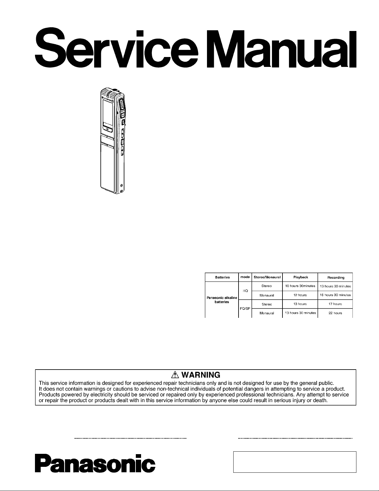
IC Recorder
Specification
Power output: 350mW(max.)
Frequencyresponse: 280Hz - 5,200Hz(HQ mode)
270Hz - 3,400Hz(FQ/SP mode)
S/N: 35dB(HQ mode)
Jack:
Outputjack; Earphone, 3.5mm(1/8in.),
0.5mW+0.5mW 16Ω
Inputjack; Mic, 3.5mm(1/8in.), 0.56mV plug in
power
Speaker: 20mm(1-3/32in.) 8Ω
Power requirement: DC 3V(2AAA/LR03 size batteries)
Dimensions (W×H×D):
Maxdimensions; 32.5×118.8×15.9mm (1-9/32×4-
11/16×5/8in.)
Cabinet dimensions; 29.8×118.5×14.2mm (1-3/16×4-
21/32×9/16in.)
Mass:
with batteries; 61g (2.15oz.)
without batteries; 38g (1.34oz.)
Operational temperature range: 0°C-40°C (32°F-104°F)
[When used at 25°C(77°F) on a flat, stable surface]
Batterylife:
*The batterylife maybe less depending on the operating conditions.
Note:
Specifications are subject to change without notice.
Mass and dimensions are approximate.
CONTENTS
Page Page
1 Accessories 3
2 Part Names
© 2005 Matsushita Electric Industrial Co., Ltd. All
rights reserved. Unauthorized copying and
distribution is a violation of law.
3

RR-US050P
3 Operation Checks and Component Replacement Procedures 3
3.1. Checking for the analog P.C.B. and digital P.C.B.
3.2. Replacement for the LCD
3.3. Replacement for the speaker
4 Schematic Diagram
4.1. Schmatic Diagram Notes
4.2. Schematic Diagram
5 Printed Circuit Board
6 Block Diagram
7 Type Illustration of IC 痴, Transistors and Diodes
8 Operation Check Mode
8.1. To Enter Operation Check
8.2. Operation Check Method
9 Troubleshooting
3
6
6
7
7
9
13
15
15
16
16
9.1. Unit won 稚 record
9.2. Cannot Delete
9.3. Unit Won 稚 play
9.4. Unit won 稚 record
9.5. Unit won 稚 play
9.6. USB Troubleshooting
10 Terminal Function of ICエs
10.1. IC4 (MN101C74FRA) :System Control / LCD Drive
11 Replaceme nt Parts List
12 Cabinet Parts Location
13 Packaging
16
19
19
19
20
20
21
22
23
23
24
27
28
2
1 Accessories
RR-US050P
· Dictation Cord(K2KC2CA00003)...................................1pc.
· USB cable
(K2KZ4CB0008)............................................1pc.
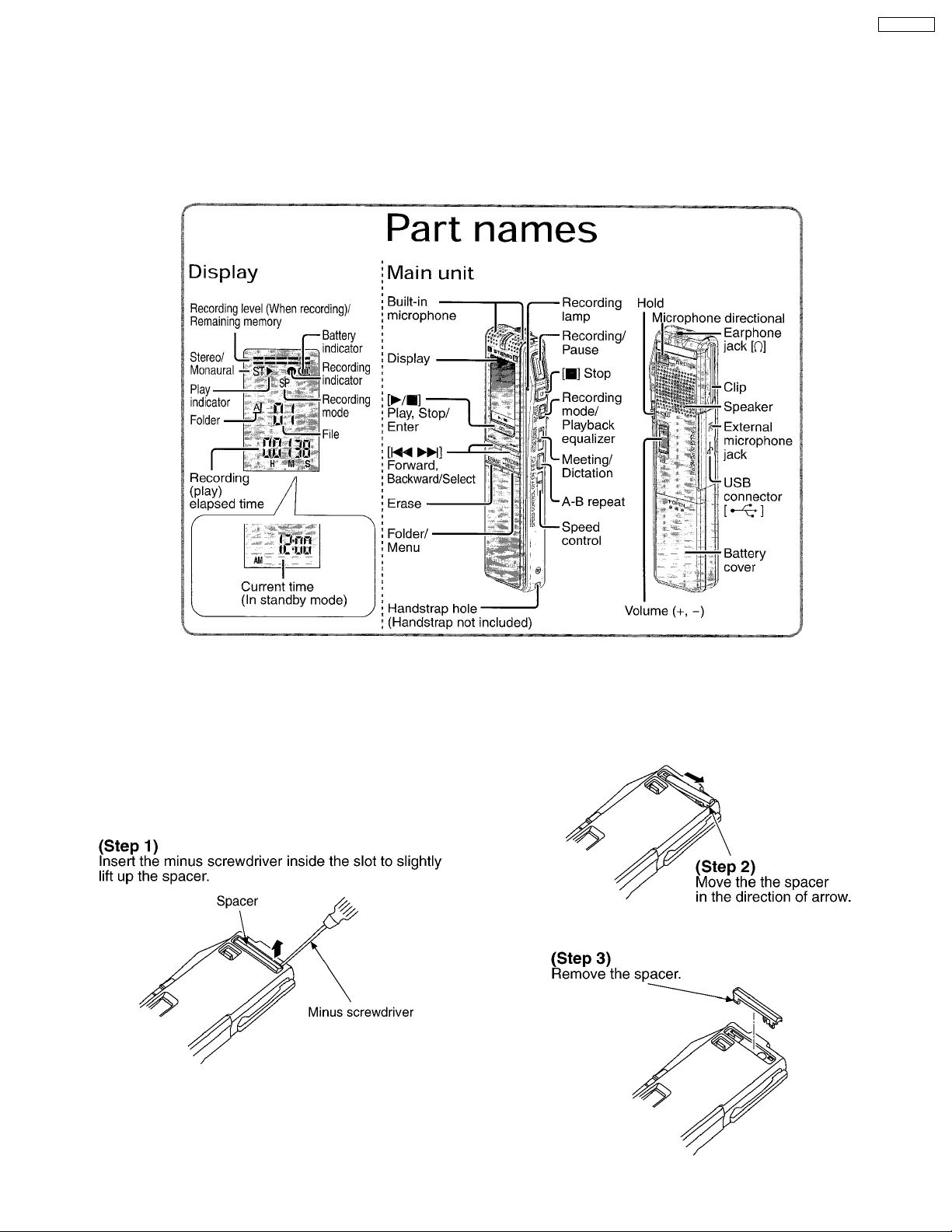
2 Part Names
· Stereo Earphones(L0BAB0000172).............................1pc.
· CD-ROM (Voice Editing) (RFE0170A-S).......................1pc.
3 Operation Checks and Component Replacement
Procedures
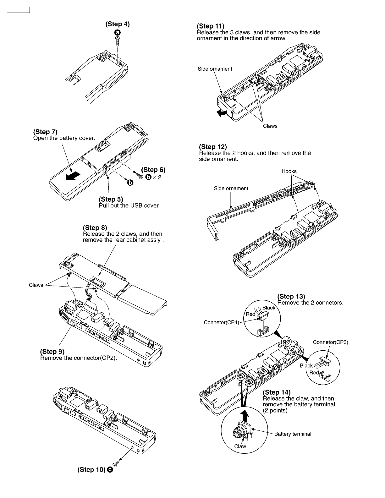
3.1. Checking for the analog P.C.B.
and digital P.C.B.
3
RR-US050P
4
RR-US050P
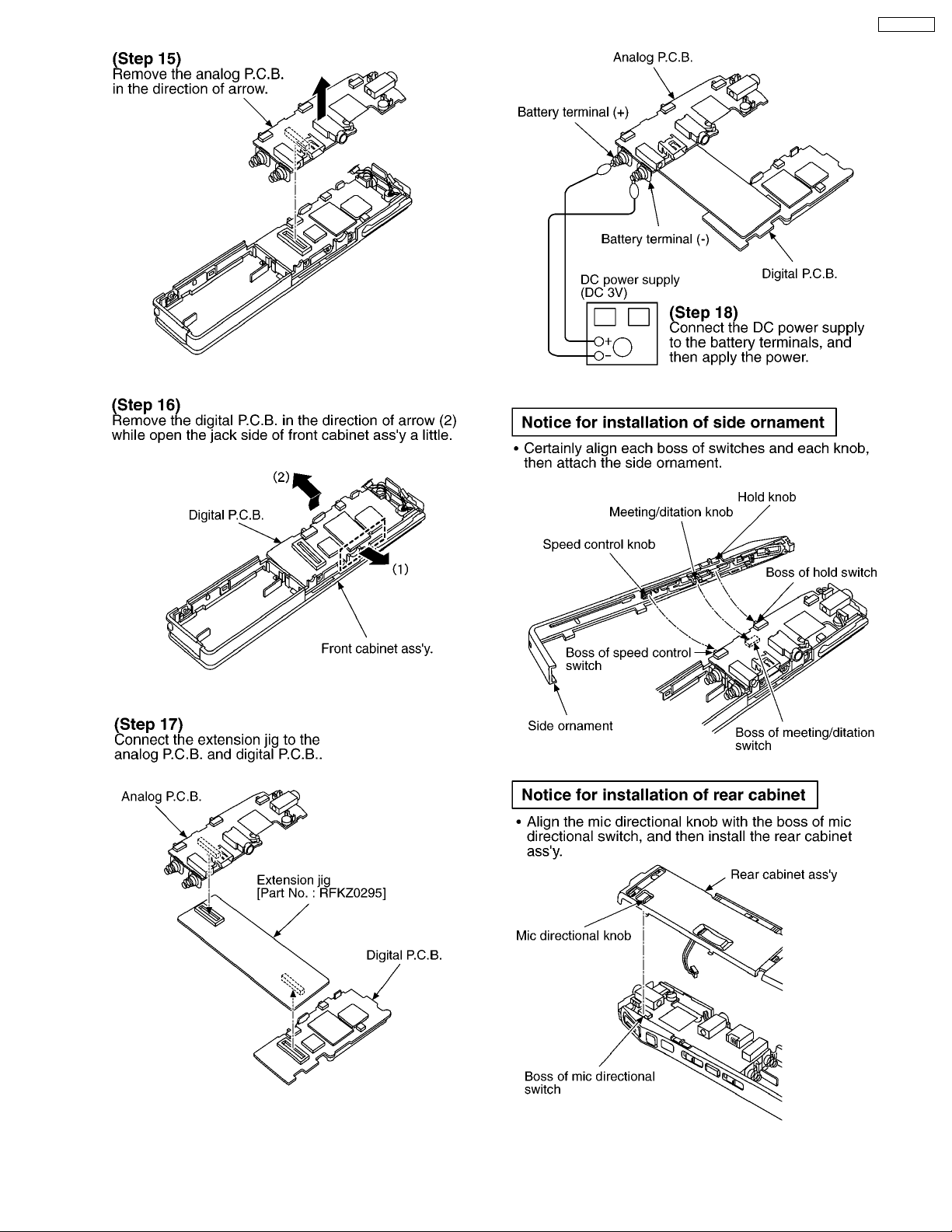
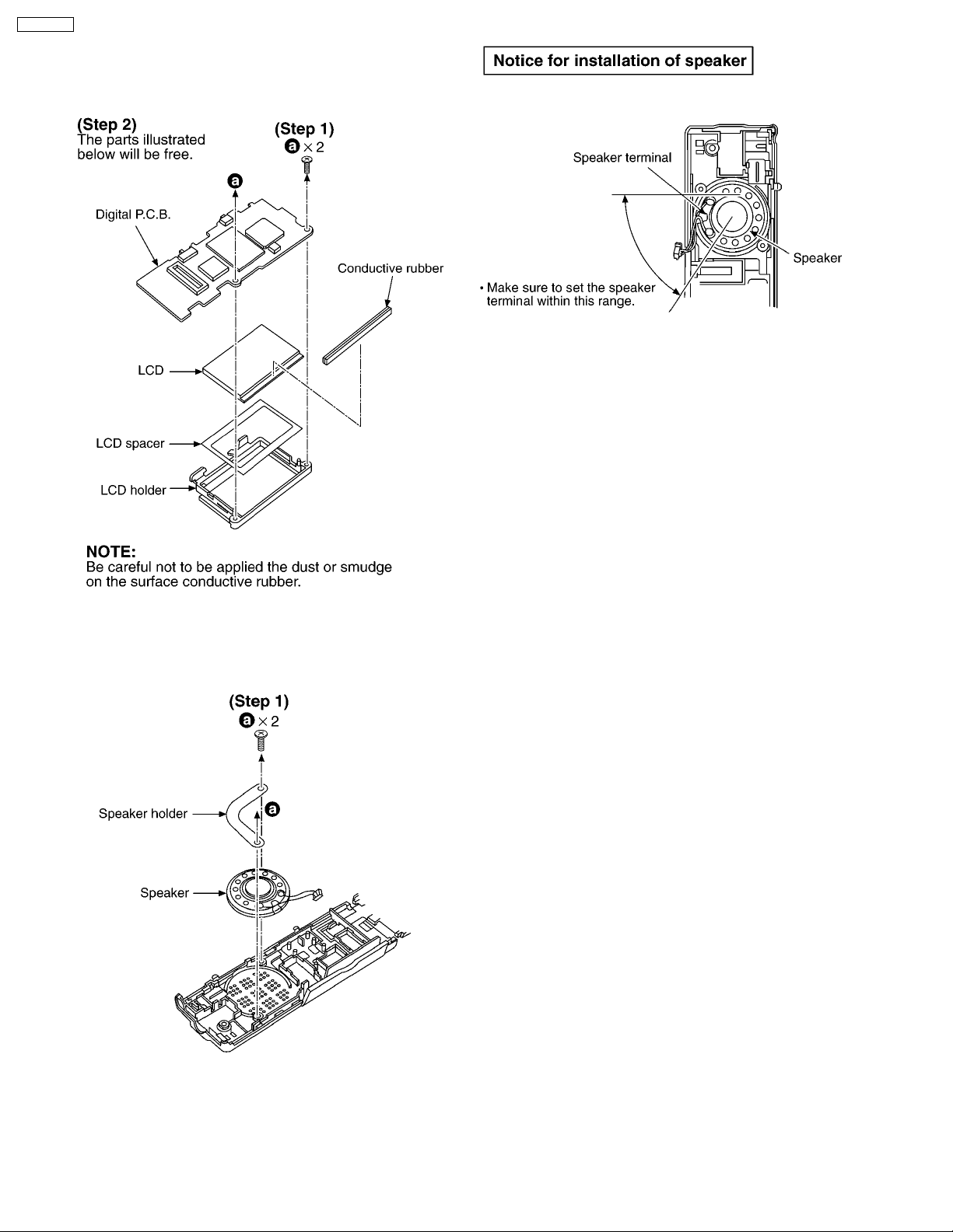
· Check the analog P.C.B. and digital P.C.B. as shown
below.
5
RR-US050P
3.2. Replacement for the LCD
· Follow the (Step 1) - (Step16) of item 3.1.1.
3.3. Replacement for the speaker
· Follow the (Step 1) - (Step 9) of item 3.1.1.
6
4 Schematic Diagram
4.1. Schmatic Diagram Notes
(This schematic diagram may be modified at any time with
development of new technology.)
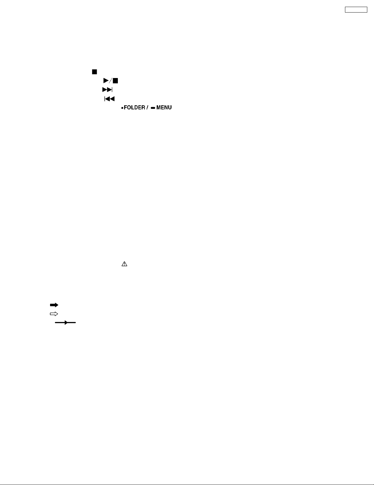
· S1 : Stop switch (
· S2 : Playback switch (
· S3 : Forward switch (
· S4 : Backward switch(
· S5 : Folder, Menu switch (
· S6 : Erase switch (ERASE).
· S7 : A-B repeat switch.
· S8 : Recording/Pause switch (REC/PAUSE).
· S9 : Volume (+) switch.
· S10 : Volume (-) switch.
· S11 : Recording mode switch (REC MODE).
· S13 : Hold switch (HOLD) in “OFF” position.
· S15 : Microphone directional switch in “OFF” position.
· S17 : Speed control switch in “OFF” position.
· S18: Meeting/Dictation select switch
(MEETING/DICTATION) in “MEETING” position.
· VR1:Volume control VR.
· DC voltage measurements are taken with electronics
voltmeter. The negative terminal of the battery provides
negative meter connec tion point.
No mark.....Recording, ( ).....Playback
· Important safety notice
Components identified by
characteristics impotant for safety.
When replacing any of components, use only
manufacturer’s specified parts.
· Signal lines
: Sound source signal (ANALOG) line
: Sound source signal (DIGITAL) line
).
).
).
).
mark have special
: Positive voltage line
RR-US050P
).
7

RR-US050P
8
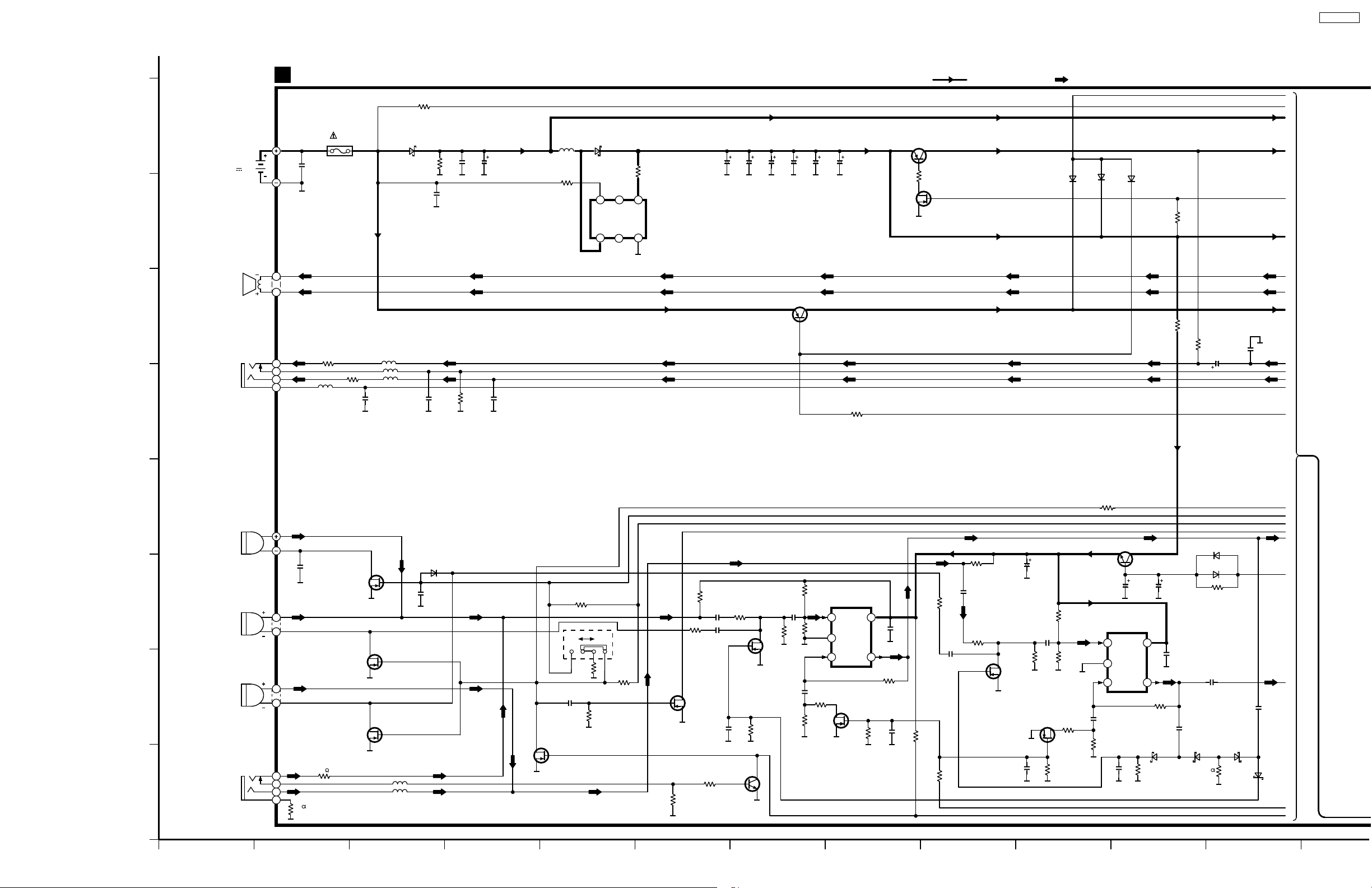
4.2. Schematic Diagram
RR-US050P
SCHEMATIC DIAGRAM-1
H
2 AAA SIZE(LR03)
BATTERIES 3V
G
SPEAKER
F
JK1
EARPHONE
E
ANALOG CIRCUIT
A
IP1
D4FBR7500008
0.1
C95
CP2
2
1
R219
2
4
3
1
47
R4 56
L2
C53
0.022
NOTE:
The number which notedat the connectors on the schematic diagramas "SCHEMATIC DIAGRAM-1" or"SCHEMATIC DIAGRAM-2"
indicates the schematic diagramserial number located on the left cornerin the schematic diagram.
R16
470K
R47
10K
L1
D2
B0JCMD000010
CE
LX
C37
C38
C212
6.3V100
100
R44
123
DD
IC8
NC
C0DBAGC00024
DC-DC CONVERTER
GND V
NC
64
5
6.3V100
Q9
B1ADKB000008
POWER SUPPLY
C211
6.3V100
6.3V100
2.9V 2.9V
2.2V
L7
L8
L4
D5
B0JCMD000010
C56
C97
0.022
R45
0.1
100K
C41
R218
0.1
C40
10V10
1M
C54
0.022
C218
6.3V100
C219
6.3V33
R72
680
Q10
B1ADKB000008
POWER SUPPLY
3V 3V
2.3V
Q13
B1CFFB000001
R39
4.7K
POWER SUPPLY
CONTROL
D
G
S
:SOUND SOURCESIGNAL(ANALOG) LINE:POSITIVE VOLTAGELINE
D26
1SS355TE17
D24
1SS355TE17
D25
1SS355TE17
R38
R41
Y
A
B
C
D
1M
E
G
H
I
10
22K
R53
C26
C55
10V4.7
0.022
J
N
K
L
M
R226
D
M1
MICROPHONE
D11
2.2V
G
0.2V
MA2S111TX
C10
0.022
0.2V
D
0V
G
S
R203
1M
S15(DIRECTIVITY)
OFFON
100K
R205
C252
0.047
2.2M
R252
Q15
B1CFFB000001
SWITCHING
R202
1M
2.2K
R209
R250
220
D
G
S
Q25
B1CFFB000001
SWITCHING
SWITCHING
1M
R201
C203
R210
0.022
4.7K
C250
0V
0.022
Q21
B1CFFB000001
SWITCHING
0.22
C254
R224
(0V)
470K
0.5V
Q5
2SD2216J0L
SWITCHING
G
R254
4.7M
R217
2.2K
IC14
1M
R208
C202
0.1
D
S
0V
R207
47K
0V
R206
C15
R10
1M
0.47
2.2K
(0V)
0.9V
(0V)
0.9V
R99
1K
C0ABAB000112
MIC AMP
DD
V
1
2
3
0V
5
+IN
GND
-IN OUT
4
Q6
B1CFFB000001
SWITCHING
D
0V
G
S
1M
R40
(0V)
1.9V
(0V)
0.9V
C92
R211
150K
C5
100P
0.01
R225
470K
R251
R59
220
10K
C251
0.022
C205
0.022
R215
4.7K
0V
G
Q22
B1CFFB000001
SWITCHING
0V
(0V)
1.4V
(0V)
1.9V
D
(0.3V)
S
D
0.2V
G
S
D
G
S
L6
L5
C200
0.022
Q20
B1CFFB000001
SWITCHING
C
M2
DIRECTIONAL
MICROPHONE
(Lch)
M3
B
A
DIRECTIONAL
MICROPHONE
(Rch)
JK2
MIC
CP3
2
1
CP4
2
1
2
4
3
1
Q12
B1CFHC000003
SWITCHING
Q1
B1CFHC000003
SWITCHING
L12
0
L3
0
4V10
C228
D
0V
R214
S
Q7
B1CFFB000001
SWITCHING
0.01
C224
1M
R213
C204
0.1
1M
47K
R216
R238
0V
SD
0V
G
1M
R239
Q17
2SD2216J0L
POWER SUPPLY
1K
10K
IC15
C0ABAB000112
MIC AMP
(0V)
0.9V
1
2
(0V)
0.9V
3
0.47
C223
2.2K
R237
C17
6.3V22
+IN
GND
-IN OUT
C19
0.22
DD
V
MA2S72800L
R12
4.7M
5
4
C255
(0V)
1.9V
(0V)
0.9V
D6
6.3V22
C91
100P
R212
150K
C60
0.1
MA2S111TX
MA2S111TX
R60 47K
C217
D7
MA2S72800L
D8
D9
0.1
0
R58
D21
MA2S72800L
D22
0.1
C253
MA2S72800L
Q
R
S
T
O
U
V
F
P
RR-US050(P) ANALOG CIRCUIT DIAGRAM
121110987654321
9
 Loading...