

Panasonic MS KX-MB283BR Schematic
Multi-Function printer
KX-MB283BR
(for Brazil)
ORDER NO. KMF0711134CE
© 2007 Panasonic Communications Co., Ltd. All
rights reserved. Unauthorized copying and distribution is a violation of law.

KX-MB283BR
TABLE OF CONTENTS
PAGE PAGE
1 Safety Precautions -----------------------------------------------3
1.1. FOR SERVICE TECHNICIANS ------------------------3
1.2. AC CAUTION -----------------------------------------------3
1.3. PERSONAL SAFETY PRECAUTIONS --------------4
1.4. SERVICE PRECAUTIONS------------------------------4
2Warning--------------------------------------------------------------5
2.1. ABOUT LEAD FREE SOLDER (PbF: Pb free)-----5
2.2. Discarding of P. C. Board --------------------------------5
2.3. INSULATION RESISTANCE TEST--------------------6
2.4. BATTERY CAUTION--------------------------------------6
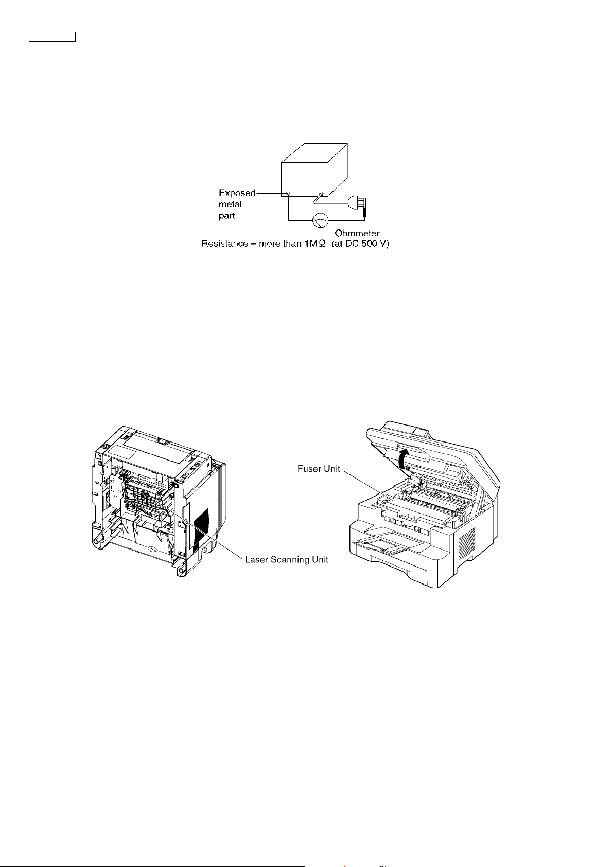
2.5. LASER BEAM AND FUSER UNIT SECTION ------6
3 Specifications------------------------------------------------------7
4 General/Introduction---------------------------------------------8
4.1. OPTIONAL ACCESSORIES----------------------------8
4.2. Translation Lists--------------------------------------------9
5Features------------------------------------------------------------10
5.1. General Features-----------------------------------------10
5.2. HARDWARE REQUIREMENTS FOR MULTIFUNCTION SOFTWARE-------------------------------10
6 Technical Descriptions----------------------------------------11
6.1. CONNECTION DIAGRAM-----------------------------11
6.2. GENERAL BLOCK DIAGRAM------------------------12
6.3. MAIN BOARD SECTION-------------------------------14
6.4. CIS CONTROL SECTION -----------------------------23
6.5. MOTOR DRIVE SECTION-----------------------------24
6.6. TIMING CHART AND WAVE FORM OF
SCANNER MOTORS -----------------------------------28
6.7. FAN MOTOR SECTION--------------------------------31
6.8. SOLENOID DRIVER SECTION----------------------33
6.9. LSU (Laser Scanning Unit) SECTION--------------34
6.10. SENSORS AND SWITCHES SECTION----------- 36
6.11. OPERATION BOARD SECTION---------------------44
6.12. LCD SECTION--------------------------------------------45
6.13. HVPS (High Voltage Power Supply)
SECTION---------------------------------------------------46
6.14. HEAT LAMP CONTROL CIRCUIT-------------------48
6.15. Main Board Section--------------------------------------53
6.16. POWER SUPPLY BOARD SECTION --------------56
6.17. Mechanical Operation-----------------------------------57
7 Location of Controls and Components------------------59
7.1. OVERVIEW------------------------------------------------59
7.2. CONTROL P ANEL---------------------------------------60
8 Installation Instructions---------------------------------------61
8.1. INSTALLATION-------------------------------------------61
8.2. CONNECTIONS------------------------------------------72
9 T est Mode----------------------------------------------------------73
9.1. TEST FUNCTIONS--------------------------------------73
10 Service Mode -----------------------------------------------------77
10.1. PROGRAMMING AND LISTS ------------------------77
10.2. USER MODE (The list below is an example of
the SYSTEM SETUP LIST the unit prints out.)---80
10.3. HISTORY (Example of a printed out list) ---------81
11 Troubleshooting Guide----------------------------------------83
11.1. USER RECOVERABLE ERRORS ------------------83
1 1 .2. TROUBLESHOOTING DETAILS---------------------85
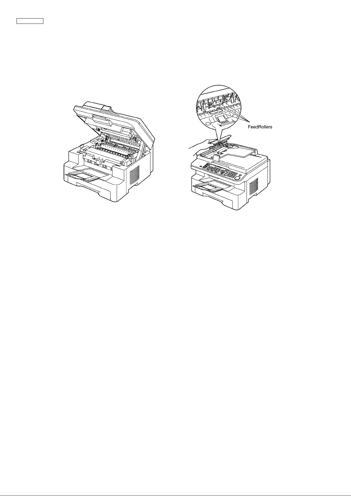
11.3. DOCUMENT JAMS (AUTO DOCUMENT
FEEDER)------------------------------------------------- 144
1 1 .4. RECORDING PAPER JAM-------------------------- 146
12 Service Fixture & Tools--------------------------------------154
13 Disassembly and Assembly Instructions -------------155
13.1. ADF SECTION ------------------------------------------156
13.2. REMOVE ADF SECTION (1)------------------------157
13.3. REMOVE ADF SECTION ----------------------------158
13.4. REMOVE TOP COVER SECTION-----------------159
13.5. REMOVE SCANNER GLASS SECTION---------160
13.6. REMOVE OPERATION PANEL SECTION ------161
13.7. LEFT SIDE SECTION---------------------------------162
13.8. REMOVE MAIN BOARD -----------------------------162
13.9. REMOVE GEAR CHASSIS SECTION------------163
13.10. REMOVE PAPER FEED ROLLER-----------------164
13.11. RIGHT SIDE SECTION-------------------------------164
13.12. REMOVE RIGHT SIDE COVER SECTION------165
13.13. LOWER SIDE CABINET SECTION ---------------166
13.14. REMOVE RIGHT CASSETTE GUIDE------------167
13.15. REMOVE PICK UP BOARD-------------------------167
13.16. REMOVE HIGH VOLTAGE POWER BOARD---168
13.17. REMOVE PICK UP ROLLER UNIT----------------169
13.18. REMOVE LOW VOLTAGE POWER BOARD ---170
13.19. REMOVE FUSER UNIT-------------------------------171
13.20. Installation Position of The Lead--------------------172
14 Maintenance-----------------------------------------------------178
14.1. MAINTENANCE ITEMS AND COMPONENT
LOCATIONS---------------------------------------------178
14.2. MAINTENANCE-----------------------------------------180
14.3. PRINTING OPERATION PRINCIPLE-------------185
14.4. TERMINAL GUIDE OF THE ICs
TRANSISTORS AND DIODES----------------------190
14.5. HOW TO REPLACE THE FLAT PACKAGE IC -192
14.6. MAIN BOARD SECTION -----------------------------194
14.7. TEST CHART--------------------------------------------196
15 Schematic Diagram-------------------------------------------198
15.1. For Schematic Diagram-------------------------------198
15.2. MAIN BOARD -------------------------------------------199
15.3. OPERATION BOARD ---------------------------------209
15.4. SENSOR BOARD --------------------------------------210
16 Printed Circuit Board-----------------------------------------212
16.1. MAIN BOARD -------------------------------------------212
16.2. OPERATION BOARD ---------------------------------214
16.3. SENSOR BOARD --------------------------------------216
17 Exploded View and Replacement Parts List----------219
17.1. CABINET, MECHANICAL AND ELECTRICAL
PARTS LOCATION-------------------------------------219
17.2. REPLACEMENT PARTS LIST ----------------------232
2
KX-MB283BR
1 Safety Precautions
1. Before servicing, unplug the AC power cord to prevent an electric shock.
2. When replacing parts, use only the manufacturer's recommended components.
3. Check the condition of the power cord. Replace if wear or damage is evident.
4. After servicing, be sure to restore the lead dress, insulation barriers, insulation papers, shields, etc.
5. Before returning the serviced equipment to the customer, be sure to perform the following insulation resistance test to prevent
the customer from being exposed to shock hazards.
1.1. FOR SERVICE TECHNICIANS
• Repair service shall be provided in accordance with repair technology information such as service manu al so as to prevent fires, injury or electric shock, which can be caused by improper repair work.
6. When repair services are provided, neither the products nor their parts or members shall be remodeled.
7. If a lead wire assembly is supplied as a repair part, the lead wire assembly shall be replaced.
8. FASTON terminals shall be plugged straight in and unplugged straight.
• ICs and LSIs are vulnerable to static electricity.
When repairing, the following precautions will help prevent recurring malfunctions.
1. Cover plastic parts boxes with aluminum foil.
2. Ground the soldering irons.
3. Use a conductive mat on worktable.
4. Do not grasp IC or LSI pins with bare fingers.
1.2. AC CAUTION
For safety, before closing the lower cabinet, please make sure of the following precautions.
1. The earth lead is fixed with the screw.
2. The AC connector is connected properly.
3
KX-MB283BR
1.3. PERSONAL SAFETY PRECAUTIONS
1.3.1. MOVING SECTIONS OF THE UNIT
Be careful not to let your hair, clothes, fingers, accessories, etc., become caught in any moving sections of the unit.
The moving sections of the unit are the rollers and a gear. There is a separation roller and a document feed roller which are rotated
by the document feed motor. A gear rotates the two rollers. Be careful not to touch them with your hands, especially when the unit
is operating.
1.3.2. LIVE ELECTRICAL SECTIONS
All the electrical sections of the unit supplied with AC powe r by the AC power cord are live.
Never disassemble the unit for service with the AC power supply plugged in.
CAUTION:
AC voltage is supplied to the primary side of the power supply unit. Therefore , always unplug the AC power cord before disassembling for service.
1.4. SERVICE PRECAUTIONS
1.4.1. PRECAUTIONS TO PREVENT DAMAGE FROM STATIC ELECTRICITY
Electrical charges accumulate on a person. For instance, clothes rubbing together can damage electric elem ents or change their
electrical characteristics. In order to prevent static electricity, touch a metallic part that is grounded to release the static electricity.
Never touch the electrical sections such as the power supply unit, etc.
4
KX-MB283BR
2Warning
2.1. ABOUT LEAD FREE SOLDER (PbF: Pb free)
Note:
In the information below, Pb, the symbol for lead in the periodic table of elements, will refer to standard solder or solder that contains lead.
We will use PbF solder when discussing the lead free solder used in our manufacturing process which is made from Tin, (Sn),
Silver, (Ag), and Copper, (Cu).
This model, and others like it, manufactured using lead free solder will have PbF stamped on the PCB. For service and repair
work we suggest using the same type of solder although, with some precautions, standard Pb solder can also be used.
Caution
• PbF solder has a melting point that is 50° ~ 70° F, (30° ~ 40°C) higher than Pb solder. Please use a soldering iron with temperature control and adjust it to 700° ± 20° F, (370° ± 10°C). In case of using high temperature soldering iron, please be careful not to
heat too long.
• PbF solder will tend to splash if it is heated much higher than its melting point, approximately 1100°F, (600°C).
• If you must use Pb solder on a PCB manufactured using PbF solder, remove as much of the original PbF solder as possible and
be sure that any remaining is melted prior to applying the Pb solder.
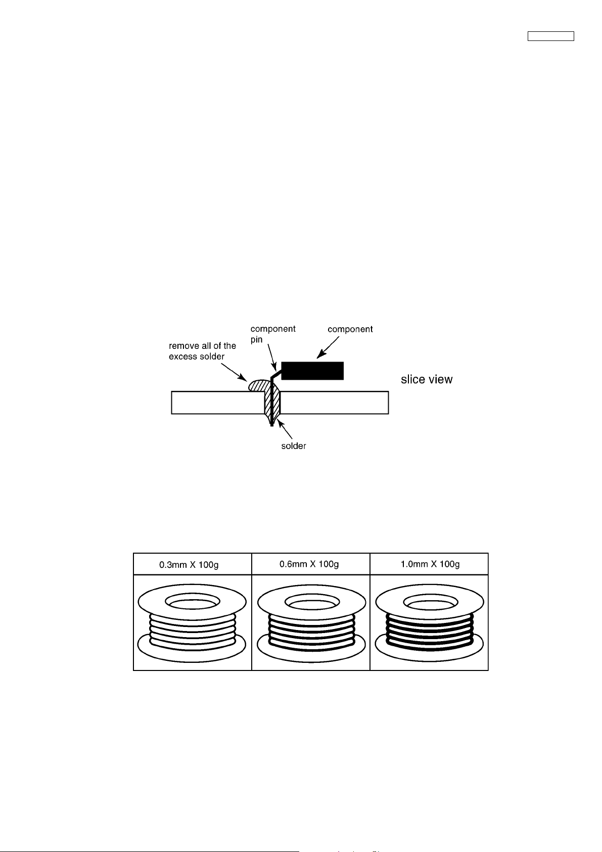
• When applying PbF solder to double layered bo ards, please check the component side for excess which may flow onto the
opposite side (See figure, below).
2.1.1. SUGGESTED PBF SOLDER
There are several types of PbF solder available commercially. While this product is manufactured using Tin, Silver, and Copper,
(Sn+Ag+Cu), you can also use Tin and Copper, (Sn+Cu), or Tin, Zinc, and Bismuth, (Sn+Zn+Bi). Please check the manufacturer’s specific instructions for the melting points of their products and any precautions for using their product with other
materials.
The following lead free (PbF) solder wire sizes are recommended for service of this product: 0.3mm, 0.6mm and 1.0mm.
2.2. Discarding of P. C. Board
When discarding P. C. Board, delete all personal information such as telephone directory and caller list or scrap P. C. Board.
5
KX-MB283BR
2.3. INSULATION RESISTANCE TEST
1. Unplug the power cord and short the two prongs of the plug with a jumper wire.
2. Turn on the pow e r switch .
3. Measure the resistance value with an ohmmeter between the jumpered AC plug and each exposed metal cabinet part
(screw heads, control shafts, bottom frame, etc.).
Note: Some exposed parts may be isolated from the chassis by design. These will read infinity.
4. If the measurement is outside the specified limits, there is a possibility of a shock hazard.
2.4. BATTERY CAUTION
CAUTION
Danger of explosion if the battery is replaced incorrectly. Replace only with the same or equivalent type recommended by the
manufacturer. Dispose used batteries according to the manufacturer’s instructions:
The lithium battery is a critical component (typ e No.CR2354). Please observe for the proper pol arity and exact location when
replacing it and the soldering the replacement litium battery in.
2.5. LASER BEAM AND FUSER UNIT SECTION
• The printer of this unit utilizes a laser. Use of controls or adjustments or performance of procedures other than those specified
herein may result in hazardous radiation exposure.
• The fuser unit is inside of the unit and gets hot. Do not touch it when removing the jammed paper or cleaning the lower glass.
6

3 Specifications
Applicable Lines: Public Switched Telephone Network
Document Size: Max. 216 mm in width
Effective Scanning Width: 208 mm
Effective Printing Width: Letter/ Legal: 208 mm
Tran sm ission Time*: Approx. 4 s/page (ECM-MMR Memory transmission)**
Scanning Density: Scanning resolution:
Photo resolution: 64-level
Scanner Type: Color Contact Image Sensor
Printer Type: Laser printer
Data Compression System: Modified Huffman (MH), Modified READ (MR), Modified Modified READ (MMR)
Operating Environment: 10 °C—32.5 °C, 20—70 % RH (Relative Humidity)
Dimensions: Approx. height 305 mm × width 420 mm × depth 445 mm
Mass (Weight): Approx. 13 kg
Power Consumption: Standby: Approx. 5.5 W
Power Supply: 127V AC, 60Hz
Memory Capacity (for operation and
storing memory):
Laser diode properties: Laser output: Max. 5 mW
Print Speed: Approx. 18 ppm (pages per minute)
Printing Resolution: 600 × 600 dpi
Max. 600 mm in length
A4: 202 mm
Up to 600 × 1,200 dpi (Optical)
Up to 9,600 × 9,600 dpi (Interpolated)
Copy resolution:
Up to 600 × 600 dpi (Scanner Glass)
Up to 600 × 300 dpi (Auto Document Feeder)
Preheat: Approx. 65 W
Copy: Approx. 320 W
Maximum: Approx. 900 W (When the fuser lamp turns on)
32 MB
Wave length: 760 nm—810 nm
Emission duration: Continuous
KX-MB283BR
* Transmission speed depends on the contents of the pages, resolution, telephone line conditions and capability of the other party’s
machine.
** Transmission speed is based on the ITU-T No. 1 Test Chart with original mode. (Refer to ITU-T No.1 TEST CHART (P.196).) If
the capability of the other party's machine is inferior to your unit, the transmission time may be longer.
Note:
• Design and specifications are subject to change without notice.
• The pictures and illustrations in these instructions may vary slightly from the actual product.
• The accuracy of the clock is approximately ±60 seconds a month.
7

KX-MB283BR
4 General/Introduction
4.1. OPTIONAL ACCESSORIES
Model No. Description Specifications
KX-FAT92A Replacement toner cartridge 1 toner cartridge
KX-FAD93A Replacement drum unit 1 drum unit
8
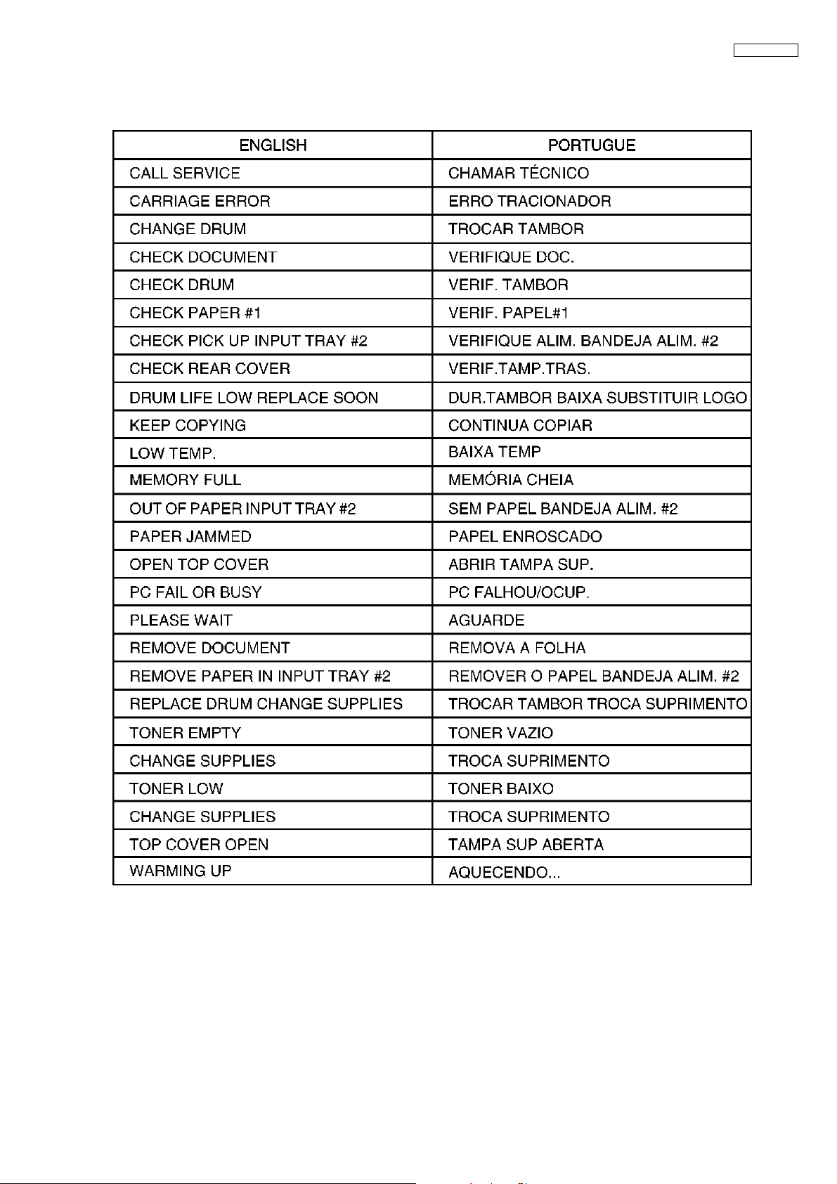
4.2. Translation Lists
4.2.1. Error Message (Display)
KX-MB283BR
9

KX-MB283BR
5Features
5.1. General Features
General
• LCD (Liquid Crystal Display) readout
250-sheet paper capacity (60 g/m
Distinctive ring detection.
2
~ 75 g/m2)
Plain Paper Facsimile Machine
Output tray (approx. 150 sheets)
Letter/A4/Legal, G3 compatible
Automatic document feeder (Up to 20 sheets)
Quick scan
Resolution: Standard/Fine/Super fine/Photo (64 level).
STANDARD: For normal-sized characters.
FINE: For small-sized characters.
SUPER FINE: For very small-sized characters.
PHOTO: For photographs, shaded drawings, etc.
Broadcast
Large Memory... Performed by DRAM
Approx. 150 pages of memory transmission
Approx. 170 pages of memory reception
Enhanced Copier Function
Multi-copy function (up to 99 copies)
Enlargement and reduction
Collate
64-Level halftone
5.2. HARDWARE REQUIREMENTS FOR MULTI-FUNCTION SOFTWARE
To use Multi-Function Station on your computer, the following are required:
Operating System:
Windows 98 / Windows Me / Windows 2000 / Windows XP / Windows Vista
CPU:
Windows 98: Pentium® 90 MHz or faster
Windows Me: Pentium 150 MHz or faster
Windows 2000: Pentium 166 MHz or faster
Windows XP: Pentium 300 MHz or faster
Windows Vista: Recent Processor (x86) 800 MHz or higher processor
RAM:
Windows 98: 24 MB (32 MB or more recommended)
Windows Me: 32 MB (64 MB or more recommended)
Windows 2000: 64 MB or more
Windows XP: 128 MB or more
Windows Vista: 512 MB or more
Other Hardware:
CD-ROM drive
Hard disk drive with at least 150 MB of available space
USB interface
LAN interface (10Base-T / 100Base-TX)
Other:
Internet Explorer® 5.0 or later
TM
operating system
10
6 Technical Descriptions
6.1. CONNECTION DIAGRAM
KX-MB283BR
11

KX-MB283BR
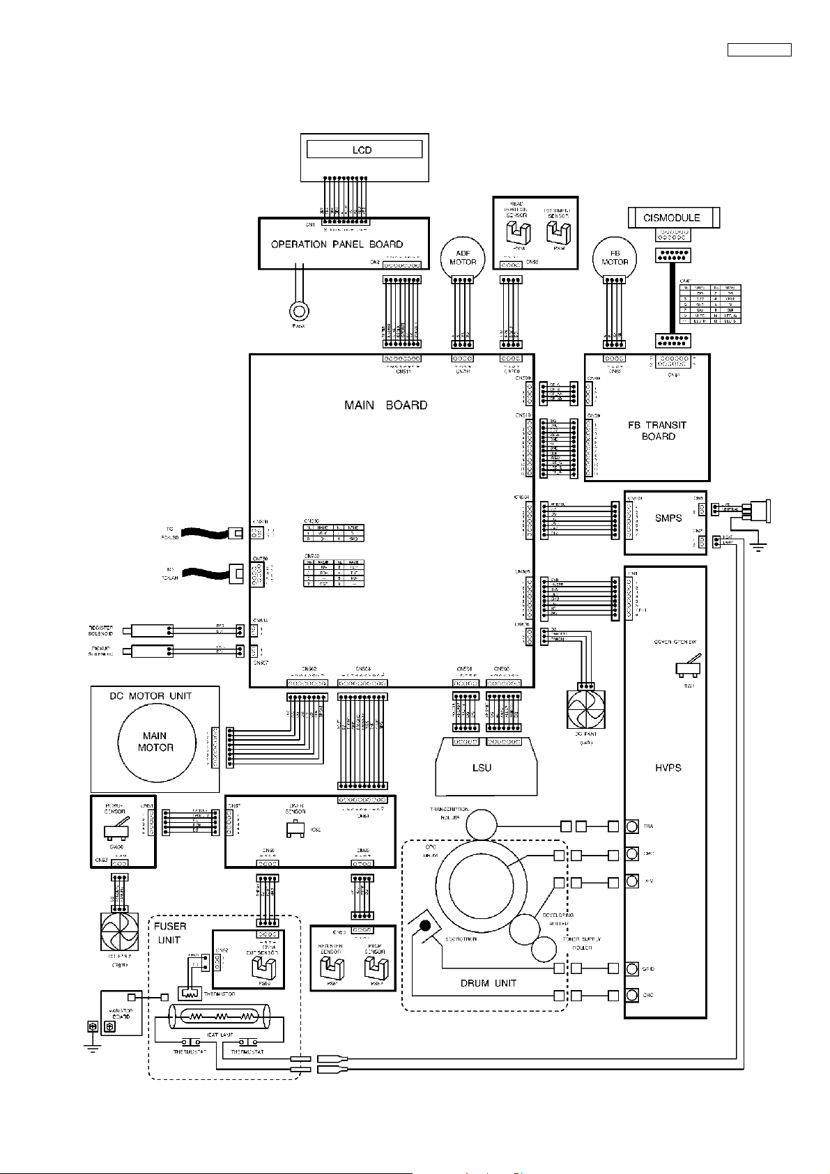
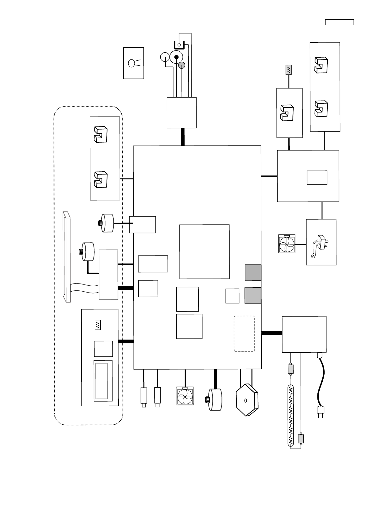
6.2. GENERAL BLOCK DIAGRAM
MAIN UNIT
SOC (IC300)
This custom IC is used for general MFP operations.
1) CPU ARM9 operating at 250MHz.
2) SDRAM Controller Controls SDRAM Memory.
3) USB Controller with PHY Apply to USB2.0 HS
4) Scanner I/F Controls the CIS and AFE, and process the scan images.
5) LSU I/F Controls the polygon motor and outputs the VIDEO signal to LSU.
6) MOTOR I/F Controls the DC motor and Stepping Motor.
7) FAN I/F Controls FAN MOTOR and detect the rotation of FAN MOTOR.
8) OPERATION PANEL I/F Serial interface with Operation Panel.
9) SENSOR I/F Detects the sensor signal.
10) I/O PORT I/O Port Interface.
11) A/D, D/A converter Sends beep tones, etc.
Convert the analog signal to the digital signal.
12) RTC Real time clock.
15) LAN Controller Ethernet Control.
ROM (IC402)
This 8MB FLASH ROM contains all of the program instructions on the unit operations.
SYNCHRONOUS DYNAMIC RAM (IC400)
This 256Mbit SDRAM is used for CPU work and receiving memory and page memory.
POWER SUPPLY
DC-DC converters generate 3.3V and 1.2V for system power.
Regurator generates 5V for peripheral devices.
READ SECTION
CIS Unit to read transmitted documents.
CIS Unit is connected to FLATBED transit Unit.
Scan data is converted by AFE(IC503).
MOTOR
This model has 1 DC motor and 2 stepping motors.
IC300 drives the DC motor for printing.
IC502 and IC700 drive the stepping motor for Auto Document Feeder motor and CIS carriage.
LSU
Forms the images on the OPC DRUM by rotating polygon motor and reflecting the laser beam against polygon.
SENSORS
Composed of 2 switches and 5 sensors.
POWER SUPPLY BOARD
Supplies +24V and +7V to the Main unit and controls the Heat Lamp.
HIGH VOLTAGE POWER SUPPLY BOARD
Supplies bias need for the printing operation: bias of the DRUM, Developing and Transcription.
FIXING UNIT
Composed heat lamp, thermistor and thermostats.
12
Varistor
Thermistor
KX-MB283BR
ePTOP S nsor
ater)
(He
CN52
or
Sens
tr
HVU
CN1
nRP Se sor
sor
CN56
CN700
CN505
8
CN50
Document Sen
t)
r (righ
AN moto
F
CN300
ADF motor
CN701
Motor
Driver
(ADF)
IC700
ge motor
Carria
er
CN60
Color CIS
nsit
CN509
Motor
Driv
(FB)
IC502
SoC
(sirius
IC300
Lite)
USB
IT SensorEX
CN53
CN65
CN64
Hole
CN63
egis e
R
CN50
CN66
or
IC
IC50
oner Sens
T
CN67
51
CN
p Sensor
Pick U
ed
ed
Flat B
Flat B
ard
Ope
2Line
eration Panel Bo
Op
CN61 CN62
Thermistor
G/A
LCD
FB Tra
CN59
(Room)
CN2
IC1
510
CN
AFE
IC503
ard
Main Bo
CN511
CN507
CN514
)
bit
IC400
(256M
SDRAM
)
FLASH
(32/64Mbit
CN506
IC402
Phy
LAN
0
CN75
t
CN504
CONVERTER
DC-DC
CN500
CN502
CN501
CN101
SWPS
inle
AC
Thermostat
rd set
AC co
lenoid
Resist So
DC motor
Pick-up Solenoid
FAN motor (left)
lygon motor
Po
(LSU)
Heater lamp
ostat
Therm
13
KX-MB283BR
6.3. MAIN BOARD SECTION
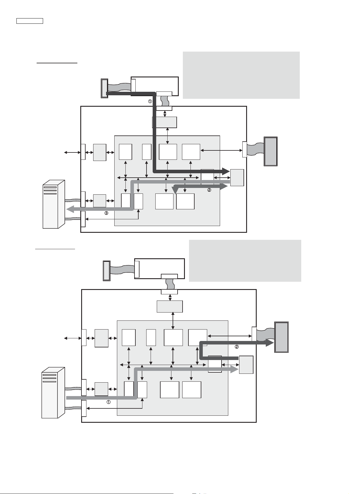
6.3.1. Data Flow
[PC Scan]
CISunit
CN61
FB transit Board
CN59
1. An analog image data is output from CISunit to IC503.
IC503 decode the analog data to digital data, and output to IC300.
Scanner I/F in IC300 process image data and store it in IC400
through SDRAM I/F.
2. If necessary, the data is compressed via DSP.
3. When you use the LAN, the data is output to PC
through the LAN I/F and PHY(IC750).
When you use the USB, the data is output to PC
through the USB I/F.
TEL
LINE
PC
LAN
USB
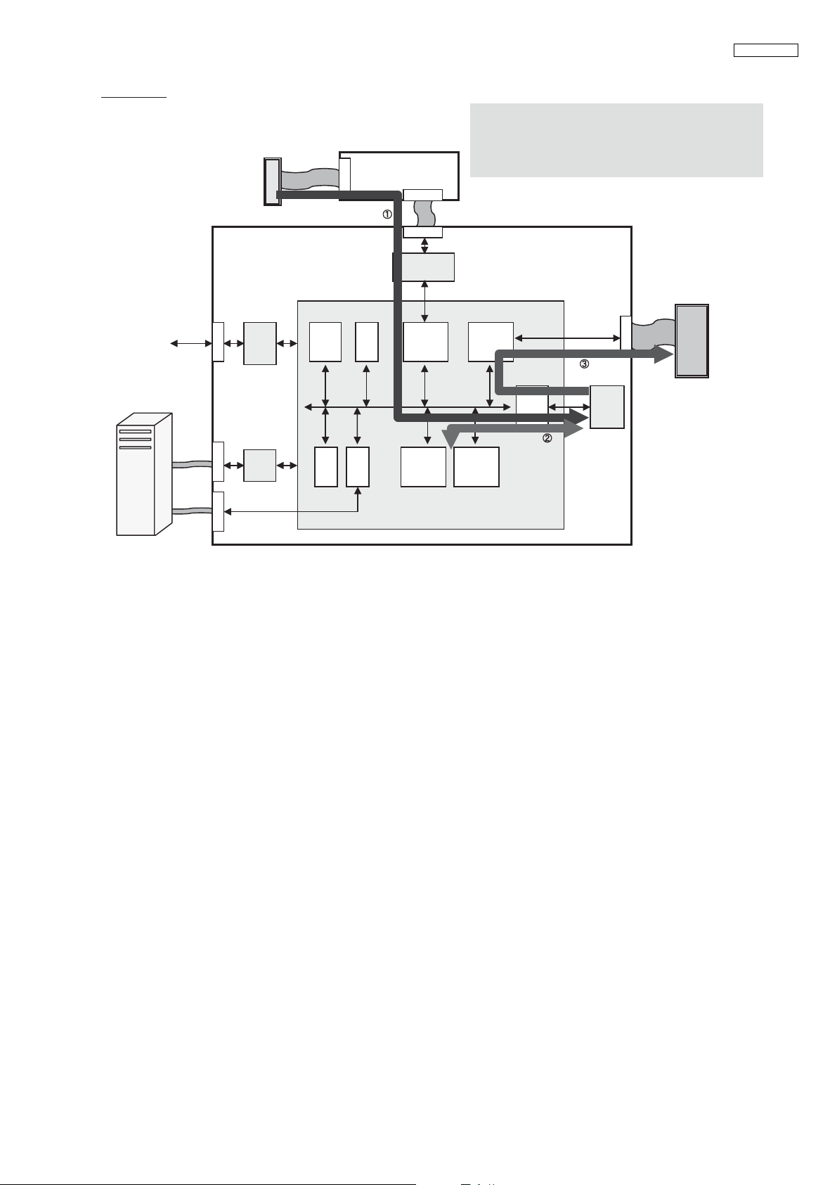
[PC print]
Main Board
IC100
IC101
DAA
CN100
IC750
PHY
CN750
CN300
CISunit
MODEM
LAN
I/F
USB
I/F
CPU
CN61
CN510
AFE
Scanner
I/F
FB transit Board
CN59
IC503
IC300
Print I/F
IC400
SDRAM
I/F
DSPJBIG
SDRAM
1.The print data is output from PC through LAN
and pass the PHY(IC750) and LAN I/F in IC300.
or
The print data is output from PC through USB
and pass the USB I/F in IC300.
then the data is stored in IC400 through SDRAM I/F.
Print I/F retrieve the data from IC400 and output it to LSU.
2.
LSU
CN500
PC
TEL
LINE
LAN
USB
Main Board
IC100
IC101
DAA
CN100
IC750
PHY
CN750
CN300
MODEM
LAN
I/F
USB
I/F
CPU
CN510
AFE
Scanner
IC503
IC300
DSPJBIG
Print I/F
SDRAM
I/F
I/F
CN500
IC400
SDRAM
LSU
14
[Copy]
CISunit
CN61
FB transit Board
CN59
1. An analog image data is output from CISunit to IC503.
IC503 decode the analog data to digital data, and output to IC300.
Scanner I/F in IC300 process image data and store it in IC400
through SDRAM I/F.
2. If necessary, the data is compressed via JBIG.
3. Print I/F retrieve the data from IC400 and output it to LSU.
KX-MB283BR
PC
TEL
LINE
LAN
USB
Main Board
IC100
IC101
DAA
CN100
IC750
PHY
CN750
CN300
MODEM
LAN
I/F
USB
I/F
CPU
CN510
AFE
Scanner
I/F
IC503
DSPJBIG
Print I/F
IC300
SDRAM
I/F
LSU
CN500
IC400
SDRAM
15

KX-MB283BR
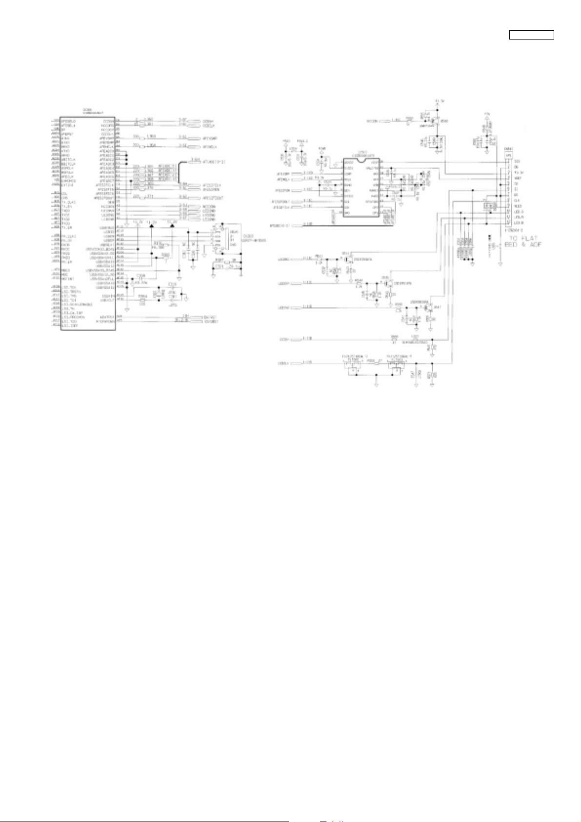
Description of Pin Distribution (IC300) SOC (System On Chip)
PIN NO. PinName I/O POWER SUPPLY VOLTAGE EXPLANATION
A02 LEDONB O 3.3V SCANNER INTERFACE
A03 NCCDON O 3.3V SCANNER INTERFACE
A04 AFEMCLK O 3.3V SCANNER INTERFACE
A05 NCCDCP O 3.3V NOT USED
A06 CCDCLK O 3.3V NOT USED
A07 PIO29 O 3.3V OPERATION PANEL INTERFACE
A08 PIO57 O 3.3V CARRIAGE MOTOR INTERFACE
A09 PIO53 O 3.3V CARRIAGE/ADF MOTOR INTERFACE
A10 PIO50 O 3.3V CARRIAGE/ADF MOTOR INTERFACE
A11 PIO46 O 3.3V FAN1 CONTROL
A12 PIO42 O 3.3V DC MOTOR INTERFACE
A13 NFRCE O 3.3V FLASH MEMORY CHIP SELECT
A14 FRMD0 I/O 3.3V FLASH MEMORY DATA BUS 0
A15 FRMD3 I/O 3.3V FLASH MEMORY DATA BUS 3
A16 FRMD7 I/O 3.3V FLASH MEMORY DATA BUS 7
A17 FRMA3 O 3.3V FLASH MEMORY ADDRESS BUS 3
A18 FRMA6 O 3.3V FLASH MEMORY ADDRESS BUS 6
A19 FRMA10 O 3.3V FLASH MEMORY ADDRESS BUS 10
A20 THRMAVDD - 3.3V POWER SUPPLY
A21 FRMA11 O 3.3V FLASH MEMORY ADDRESS BUS 11
A22 FRMA15 O 3.3V FLASH MEMORY ADDRESS BUS 15
A23 FRMA17 O 3.3V FLASH MEMORY ADDRESS BUS 17
A24 FRMA20 O 3.3V FLASH MEMORY ADDRESS BUS 20
A25 FRMA22 O 3.3V FLASH MEMORY ADDRESS BUS 22
AA01 SDMD8 I/O 3.3V SDRAM DATA BUS 8
AA02 SDMD9 I/O 3.3V SDRAM DATA BUS 9
AA03 SDMA7 O 3.3V SDRAM ADDRESS BUS 7
AA04 SDMA6 O 3.3V SDRAM ADDRESS BUS 6
AA23 VDD1.2 - 1.2V POWER SUPPLY
AA24 AFERST O 3.3V NCU INTERFACE
AA25 RING I 3.3V NCU INTERFACE
AA26 EXTINT I 3.3V NCU INTERFACE
AB01 SDMD10 I/O 3.3V SDRAM DATA BUS 10
AB02 SDMD11 I/O 3.3V SDRAM DATA BUS 11
AB03 SDMA5 O 3.3V SDRAM ADDRESS BUS 5
AB04 VDD1.2 - 1.2V POWER SUPPLY
AB23 VSS - GND GND
AB24 BTXD O 3.3V NCU INTERFACE
AB25 BRXD I 3.3V NCU INTERFACE
AB26 AFECLK O 3.3V NCU INTERFACE
AC01 SDMD12 I/O 3.3V SDRAM DATA BUS 12
AC02 SDMD13 I/O 3.3V SDRAM DATA BUS 13
AC03 SDMA4 O 3.3V SDRAM ADDRESS BUS 4
AC04 VSS - GND GND
AC05 VSS - GND GND
AC06 VDD1.2 - 1.2V POWER SUPPLY
AC07 TXD0 O 3.3V ETHERNET INTERFACE
AC08 TX_ER O 3.3V ETHERNET INTERFACE
AC09 RXD1 I 3.3V ETHERNET INTERFACE
AC10 VDD3.3 - 3.3V POWER SUPPLY
AC11 TEST I 3.3V NOT USED
AC12 USBREXT I 3.3V USB INTERFACE
AC13 VDD1.2 - 1.2V POWER SUPPLY
AC14 VDD3.3 - 3.3V POWER SUPPLY
AC15 USBXIN I 3.3V CRYSTAL(12MHz) INPUT
AC16 LSI_SCAN_ENABLE I 3.3V NOT USED
AC17 VDD1.2 - 1.2V POWER SUPPLY
AC18 NWDTRST O 3.3V WATCH DOG TIMER RESET OUTPUT
AC19 LSI_TN I 3.3V NOT USED
AC20 PSCIO2 I 3.3V INPUT PORT (FANDET1)
AC21 PSCIO6 O 3.3V NOT USED
AC22 VDD1.2 - 1.2V POWER SUPPLY
AC23 VSS - GND GND
AC24 ATXD O 3.3V NCU INTERFACE
AC25 BBITCLK I/O 3.3V NCU INTERFACE
16

PIN NO. PinName I/O POWER SUPPLY VOLTAGE EXPLANATION
AC26 BSPCLK I/O 3.3V NCU INTERFACE
AD01 SDMD14 I/O 3.3V SDRAM DATA BUS 14
AD02 SDMD15 I/O 3.3V SDRAM DATA BUS 15
AD03 VSS - GND GND
AD04 NBATRST I 3.3V BATTERY RESET INPUT
AD05 VDD2RTC - 1.2V POWER SUPPLY
AD06 CRS I 3.3V ETHERNET INTERFACE
AD07 TXD1 O 3.3V ETHERNET INTERFACE
AD08 RX_DV I 3.3V ETHERNET INTERFACE
AD09 RXD2 I 3.3V ETHERNET INTERFACE
AD10 RX_ER I 3.3V ETHERNET INTERFACE
AD11 CLKSEL I 3.3V NOT USED
AD12 USBVSSA33_BIAS - GND GND
AD13 USBVSSA33 - GND GND
AD14 USBVDDA12_SQ - 1.2V POWER SUPPLY
AD15 USBVSSA12 - GND GND
AD16 LSI_TRSTN I 3.3V NOT USED
AD17 LSI_TDO O 3.3V NOT USED
AD18 NRST I 3.3V SYSTEM RESET INPUT
AD19 HTRCTL O 3.3V HEATER CONTROL
AD20 PSCIO3 I 3.3V INPUT PORT (POUT)
AD21 PSCIO7 O 3.3V NOT USED
AD22 PSCIO15 I 3.3V INPUT PORT (RPS)
AD23 NC - - NOT USED
AD24 VSS - GND GND
AD25 ASPCLK I/O 3.3V NCU INTERFACE
AD26 ARXD I 3.3V NCU INTERFACE
AE01 SDLDM1 O 3.3V SDRAM DQML1
AE02 VSS - GND GND
AE03 SYSPLLVSS1 - GND GND
AE04 RTCCLKOUT O 3.3V CRYSTAL(32.768KHz) OUTPUT
AE05 RTCPWRDWN I 3.3V RTC POWER DOWN
AE06 TX_CLKI I 3.3V ETHERNET INTERFACE
AE07 TXD2 O 3.3V ETHERNET INTERFACE
AE08 RX_CLKI I 3.3V ETHERNET INTERFACE
AE09 RXD3 I 3.3V ETHERNET INTERFACE
AE10 MDC O 3.3V ETHERNET INTERFACE
AE11 NC - - NOT USED
AE12 USBID O 3.3V NOT USED
AE13 USBDM I/O 3.3V USB INTERFACE
AE14 USBVSSA12_SQ - GND GND
AE15 USBVDDA12PLL - 1.2V POWER SUPPLY
AE16 USBVDDA12 - 1.2V POWER SUPPLY
AE17 LSI_TDI I 3.3V NOT USED
AE18 LSI_PROCMON O 3.3V NOT USED
AE19 LSI_IDDT I 3.3V NOT USED
AE20 PSCIO1 I 3.3V INPUT PORT (PICK)
AE21 PSCIO5 O 3.3V NOT USED
AE22 PSCIO13 I 3.3V INPUT PORT (TNR)
AE23 MDMCLKOUT O 3.3V CRYSTAL(24.576MHz) OUTPUT
AE24 MDMPLLVDD - 3.3V POWER SUPPLY
AE25 VSS - GND GND
AE26 ABITCLK I/O 3.3V NCU INTERFACE
AF02 SYSPLLVDD1 - 3.3V POWER SUPPLY
AF03 VDD3.3OSC - 3.3V POWER SUPPLY
AF04 RTCCLKIN I 3.3V CRYSTAL(32.768KHz) INPUT
AF05 COL I 3.3V ETHERNET INTERFACE
AF06 TX_EN O 3.3V ETHERNET INTERFACE
AF07 TXD3 O 3.3V ETHERNET INTERFACE
AF08 RXD0 I 3.3V ETHERNET INTERFACE
AF09 MDIO I/O 3.3V ETHERNET INTERFACE
AF10 MGTINT I 3.3V ETHERNET INTERFACE
AF11 USBVBUS O 3.3V USB INTERFACE
AF12 USBVDDA33_BIAS - 3.3V POWER SUPPLY
AF13 USBDP I/O 3.3V USB INTERFACE
AF14 USBVDDA33 - 3.3V POWER SUPPLY
AF15 USBVSSA12PLL - GND GND
KX-MB283BR
17

KX-MB283BR
PIN NO. PinName I/O POWER SUPPLY VOLTAGE EXPLANATION
AF16 USBXOUT I 3.3V CRYSTAL(12MHz) OUTPUT
AF17 LSI_TMS I 3.3V NOT USED
AF18 LSI_TCK I 3.3V NOT USED
AF19 LSI_CW_TAP I 3.3V NOT USED
AF20 PSCIO0 I 3.3V INPUT PORT (REGIST)
AF21 PSCIO4 O 3.3V NOT USED
AF22 PSCIO12 I 3.3V INPUT PORT (POUT)
AF23 PSCIO14 I 3.3V INPUT PORT (DOCU)
AF24 MDMCLKIN I 3.3V CRYSTAL(24.576MHz) INPUT
AF25 MDMPLLVSS - GND GND
B01 AFEADC0 I 3.3V NOT USED
B02 VSS - GND GND
B03 LEDONG O 3.3V SCANNER INTERFACE
B04 AFERSMP O 3.3V NOT USED
B05 AFEVSMP O 3.3V SCANNER INTERFACE
B06 NCCDRS O 3.3V SCANNER INTERFACE
B07 PIO30 I/O 3.3V OPERATION PANEL INTERFACE
B08 MMPWR O 3.3V NOT USED
B09 PIO54 O 3.3V CARRIAGE/ADF MOTOR INTERFACE
B10 PIO51 O 3.3V CARRIAGE/ADF MOTOR INTERFACE
B11 PIO47 O 3.3V NOT USED
B12 PIO43 O 3.3V DC MOTOR INTERFACE
B13 NFROE O 3.3V FLASH MEMORY CHIP OUTPUT ENABLE
B14 FRMD1 I/O 3.3V FLASH MEMORY DATA BUS 1
B15 FRMD4 I/O 3.3V FLASH MEMORY DATA BUS 4
B16 FRMA0 O 3.3V FLASH MEMORY ADDRESS BUS 0
B17 FRMA4 O 3.3V FLASH MEMORY ADDRESS BUS 4
B18 FRMA7 O 3.3V FLASH MEMORY ADDRESS BUS 7
B19 THRMAVSS - GND GND
B20 TONE O 3.3V ANALOG(TONE) OUTPUT
B21 FRMA12 O 3.3V FLASH MEMORY ADDRESS BUS 12
B22 FRMA16 O 3.3V FLASH MEMORY ADDRESS BUS 16
B23 FRMA19 O 3.3V FLASH MEMORY ADDRESS BUS 19
B24 FRMA21 O 3.3V FLASH MEMORY ADDRESS BUS 21
B25 VSS - GND GND
B26 DOTPLLVSS - GND GND
C01 AFEADC3 I 3.3V NOT USED
C02 AFEADC1 I 3.3V NOT USED
C03 VSS - GND GND
C04 LEDONR O 3.3V SCANNER INTERFACE
C05 OEB O 3.3V NOT USED
C06 CCDSH O 3.3V SCANNER INTERFACE
C07 PIO31 O 3.3V OPERATION PANEL INTERFACE
C08 OPMPWR O 3.3V NOT USED
C09 PIO55 O 3.3V CARRIAGE/ADF MOTOR INTERFACE
C10 PIO52 O 3.3V CARRIAGE/ADF MOTOR INTERFACE
C11 PIO49 O 3.3V OUTPUT PORT(HSSPMUTE)
C12 PIO45 O 3.3V DC MOTOR INTERFACE
C13 NFRWE O 3.3V FLASH MEMORY CHIP WRITE ENABLE
C14 FRMD2 I/O 3.3V FLASH MEMORY DATA BUS 2
C15 FRMD6 I/O 3.3V FLASH MEMORY DATA BUS 6
C16 FRMA2 O 3.3V FLASH MEMORY ADDRESS BUS 2
C17 FRMA5 O 3.3V FLASH MEMORY ADDRESS BUS 5
C18 FRMA9 O 3.3V FLASH MEMORY ADDRESS BUS 9
C19 THRMSTR0 I 3.3V ANALOG INPUT(THERMISTOR)
C20 TONEAVDD - 3.3V POWER SUPPLY
C21 FRMA14 O 3.3V FLASH MEMORY ADDRESS BUS 14
C22 FRMA18 O 3.3V FLASH MEMORY ADDRESS BUS 18
C23 FRMA23 O 3.3V FLASH MEMORY ADDRESS BUS 23
C24 VSS - GND GND
C25 DOTPLLVDD - 3.3V POWER SUPPLY
C26 DOTCLKIN I 3.3V CRYSTAL(20MHz) INPUT
D01 AFEADC5 I 3.3V SCANNER INTERFACE
D02 AFEADC4 I 3.3V SCANNER INTERFACE
D03 AFEADC2 I 3.3V NOT USED
D04 VSS - GND GND
D05 VSS - GND GND
18

PIN NO. PinName I/O POWER SUPPLY VOLTAGE EXPLANATION
D06 VDD1.2 - 1.2V POWER SUPPLY
D07 PIO32 O 3.3V OPERATION PANEL INTERFACE
D08 CRMPWR O 3.3V MOTOR CURRENT CONTROL
D09 PIO56 O 3.3V ADF MOTOR INTERFACE
D10 VDD1.2 - 1.2V POWER SUPPLY
D11 PIO48 O 3.3V FAN2 CONTROL
D12 PIO44 O 3.3V DC MOTOR INTERFACE
D13 VDD3.3 - 3.3V POWER SUPPLY
D14 VDD1.2 - 1.2V POWER SUPPLY
D15 FRMD5 I/O 3.3V FLASH MEMORY DATA BUS 5
D16 FRMA1 O 3.3V FLASH MEMORY ADDRESS BUS 1
D17 VDD3.3 - 3.3V POWER SUPPLY
D18 FRMA8 O 3.3V FLASH MEMORY ADDRESS BUS 8
D19 THRMSTR1 I 3.3V ANALOG INPUT(THERMISTOR)
D20 TONEAVSS - GND GND
D21 FRMA13 O 3.3V FLASH MEMORY ADDRESS BUS 13
D22 VDD1.2 - 1.2V POWER SUPPLY
D23 VSS - GND GND
D24 NC - - NOT USED
D25 DOTCLKOUT O 3.3V CRYSTAL(20MHz) OUTPUT
D26 PIO66 O 3.3V NOT USED
E01 SDUDM0 O 3.3V SDRAM DQMU0
E02 AFEADC7 I 3.3V SCANNER INTERFACE
E03 AFEADC6 I 3.3V SCANNER INTERFACE
E04 VSS - GND GND
E23 VDD1.2 - 1.2V POWER SUPPLY
E24 FRMA24 O 3.3V FLASH MEMORY ADDRESS BUS 24
E25 PIO65 O 3.3V NOT USED
E26 PIO64 O 3.3V NOT USED
F01 SDMD16 I/O 3.3V SDRAM DATA BUS 16
F02 SDMD17 I/O 3.3V SDRAM DATA BUS 17
F03 AFESIFCLK O 3.3V SCANNER INTERFACE
F04 VDD1.2 - 1.2V POWER SUPPLY
F23 PIO24 I 3.3V LSU INTERFACE
F24 PIO61 O 3.3V OUTPUT PORT(SPMUTE)
F25 PIO60 O 3.3V NOT USED
F26 PIO3 O 3.3V LSU INTERFACE
G01 SDMD18 I/O 3.3V SDRAM DATA BUS 18
G02 SDMD19 I/O 3.3V SDRAM DATA BUS 19
G03 AFESIFDIN I 3.3V SCANNER INTERFACE
G04 AFESIFEN O 3.3V SCANNER INTERFACE
G23 PSCIO24 I 3.3V LSU INTERFACE
G24 PIO2 O 3.3V LSU INTERFACE
G25 PIO59 O 3.3V LAN CONTROLLER RESET
G26 PIO58 O 3.3V OUTPUT PORT(CIDRLY)
H01 SDMD20 I/O 3.3V SDRAM DATA BUS 20
H02 SDMD21 I/O 3.3V SDRAM DATA BUS 21
H03 NSDCS2 O 3.3V SDRAM CHIP SELECT 2
H04 AFESIFDOUT O 3.3V SCANNER INTERFACE
H23 PIO63 O 3.3V LSU INTERFACE
H24 PIO62 O 3.3V LSU INTERFACE
H25 PIO28 O 3.3V NOT USED
H26 PIO21 O 3.3V LSU INTERFACE
J01 SDMD22 I/O 3.3V SDRAM DATA BUS 22
J02 SDMD23 I/O 3.3V SDRAM DATA BUS 23
J03 SDMA3 O 3.3V SDRAM ADDRESS BUS 3
J04 SDMA2 O 3.3V SDRAM ADDRESS BUS 2
J23 PIO6 O 3.3V HIGH VOLTAGE UNIT INTERFACE
J24 PIO27 O 3.3V NOT USED
J25 PIO5 O 3.3V HIGH VOLTAGE UNIT INTERFACE
J26 PIO4 O 3.3V HIGH VOLTAGE UNIT INTERFACE
K01 VSS - GND GND
K02 SDCLK2 O 3.3V SDRAM CLOCK 2
K03 VSS - GND GND
K04 VDD3.3 - 3.3V POWER SUPPLY
K23 VDD1.2 - 1.2V POWER SUPPLY
K24 PIO41 O 3.3V NOT USED
KX-MB283BR
19

KX-MB283BR
PIN NO. PinName I/O POWER SUPPLY VOLTAGE EXPLANATION
K25 PIO40 O 3.3V NOT USED
K26 PIO39 O 3.3V NOT USED
L01 SDMD24 I/O 3.3V SDRAM DATA BUS 24
L02 SDMD25 I/O 3.3V SDRAM DATA BUS 25
L03 SDMA1 O 3.3V SDRAM ADDRESS BUS 1
L04 SDMAÇO O 3.3V SDRAM ADDRESS BUS 0
L11 VSS - GND GND
L12 VSS - GND GND
L13 VSS - GND GND
L14 VSS - GND GND
L15 VSS - GND GND
L16 VSS - GND GND
L23 PIO37 I 3.3V INPUT PORT (RING)
L24 PIO38 O 3.3V NOT USED
L25 PIO36 O 3.3V NOT USED
L26 PIO35 O 3.3V NOT USED
M01 SDMD26 I/O 3.3V SDRAM DATA BUS 26
M02 SDMD27 I/O 3.3V SDRAM DATA BUS 27
M03 SDMA10 O 3.3V SDRAM ADDRESS BUS 10
M04 SDBA1 O 3.3V SDRAM BANK ADDRESS 1
M11 VSS - GND GND
M12 VSS - GND GND
M13 VSS - GND GND
M14 VSS - GND GND
M15 VSS - GND GND
M16 VSS - GND GND
M23 PIO33 O 3.3V NOT USED
M24 PIO34 O 3.3V NOT USED
M25 PIO26 O 3.3V NOT USED
M26 PIO25 O 3.3V OUTPUT PORT(CNGMUTE)
N01 SDMD28 I/O 3.3V SDRAM DATA BUS 28
N02 SDMD29 I/O 3.3V SDRAM DATA BUS 29
N03 SDBA0 O 3.3V SDRAM BANK ADDRESS 0
N04 VDD1.2 - 1.2V POWER SUPPLY
N11 VSS - GND GND
N12 VSS - GND GND
N13 VSS - GND GND
N14 VSS - GND GND
N15 VSS - GND GND
N16 VSS - GND GND
N23 VDD3.3 - 3.3V POWER SUPPLY
N24 PIO23 O 3.3V NOT USED
N25 PIO22 O 3.3V NOT USED
N26 PIO20 O 3.3V NOT USED
P01 SDMD30 I/O 3.3V SDRAM DATA BUS 30
P02 SDMD31 I/O 3.3V SDRAM DATA BUS 31
P03 NSDCS O 3.3V SDRAM CHIP SELECT 1
P04 VDD3.3 - 3.3V POWER SUPPLY
P11 VSS - GND GND
P12 VSS - GND GND
P13 VSS - GND GND
P14 VSS - GND GND
P15 VSS - GND GND
P16 VSS - GND GND
P23 VDD1.2 - 1.2V POWER SUPPLY
P24 PIO16 O 3.3V NOT USED
P25 PIO17 O 3.3V NOT USED
P26 PIO18 I 3.3V HIGH VOLTAGE UNIT INTERFACE
R01 SDUDM1 O 3.3V SDRAM DQMU1
R02 SDLDM0 O 3.3V SDRAM DQML0
R03 BZVDD33 - 3.3V POWER SUPPLY
R04 BZRST33 - 3.3V POWER SUPPLY
R11 VSS - GND GND
R12 VSS - GND GND
R13 VSS - GND GND
R14 VSS - GND GND
R15 VSS - GND GND
20

PIN NO. PinName I/O POWER SUPPLY VOLTAGE EXPLANATION
R16 VSS - GND GND
R23 PIO13 O 3.3V NOT USED
R24 PIO12 O 3.3V NOT USED
R25 PIO14 O 3.3V NOT USED
R26 PIO15 O 3.3V NOT USED
T01 SDMD0 I/O 3.3V SDRAM DATA BUS 0
T02 SDMD1 I/O 3.3V SDRAM DATA BUS 1
T03 NSDCAS O 3.3V SDRAM CAS
T04 NSDRAS O 3.3V SDRAM RAS
T11 VSS - GND GND
T12 VSS - GND GND
T13 VSS - GND GND
T14 VSS - GND GND
T15 VSS - GND GND
T16 VSS - GND GND
T23 PIO9 O 3.3V OUTPUT PORT(SNPICK)
T24 PIO8 O 3.3V NOT USED
T25 PIO10 O 3.3V NOT USED
T26 PIO11 O 3.3V OUTPUT PORT(SNREG)
U01 SDMD2 I/O 3.3V SDRAM DATA BUS 2
U02 SDMD3 I/O 3.3V SDRAM DATA BUS 3
U03 NSDWE O 3.3V SDRAM WRITE ENABLE
U04 VDD1.2 - 1.2V POWER SUPPLY
U23 VDD3.3 - 3.3V POWER SUPPLY
U24 PIO0 I 3.3V INPUT PORT (HOOK)
U25 PIO1 O 3.3V OUTPUT PORT(EXTRLY)
U26 PIO7 O 3.3V NOT USED
V01 SDMD4 I/O 3.3V SDRAM DATA BUS 4
V02 SDMD5 I/O 3.3V SDRAM DATA BUS 5
V03 SDCKE O 3.3V SDRAM CLOCK ENABLE
V04 SDMA12 O 3.3V SDRAM ADDRESS BUS 12
V23 PSCIO20 O 3.3V NOT USED
V24 PSCIO21 O 3.3V NOT USED
V25 PSCIO22 O 3.3V NOT USED
V26 PSCIO23 O 3.3V NOT USED
W01 SDMD6 I/O 3.3V SDRAM DATA BUS 6
W02 SDMD7 I/O 3.3V SDRAM DATA BUS 7
W03 SDMA11 O 3.3V SDRAM ADDRESS BUS 11
W04 SDMA9 O 3.3V SDRAM ADDRESS BUS 9
W23 PSCIO16 O 3.3V NOT USED
W24 PSCIO17 I 3.3V INPUT PORT (FANDET2)
W25 PSCIO18 I 3.3V INPUT PORT (TOPCVR)
W26 PSCIO19 I 3.3V INPUT PORT (PSTART)
Y01 VSS - GND GND
Y02 SDCLK O 3.3V SDRAM CLOCK 1
Y03 SDMA8 O 3.3V SDRAM ADDRESS BUS 8
Y04 VSS - GND GND
Y23 AFESEL0 I 3.3V NCU INTERFACE
Y24 AFESEL1 I 3.3V NCU INTERFACE
Y25 EXMDMCS O 3.3V NOT USED
Y26 DP O 3.3V NCU INTERFACE
KX-MB283BR
21
KX-MB283BR
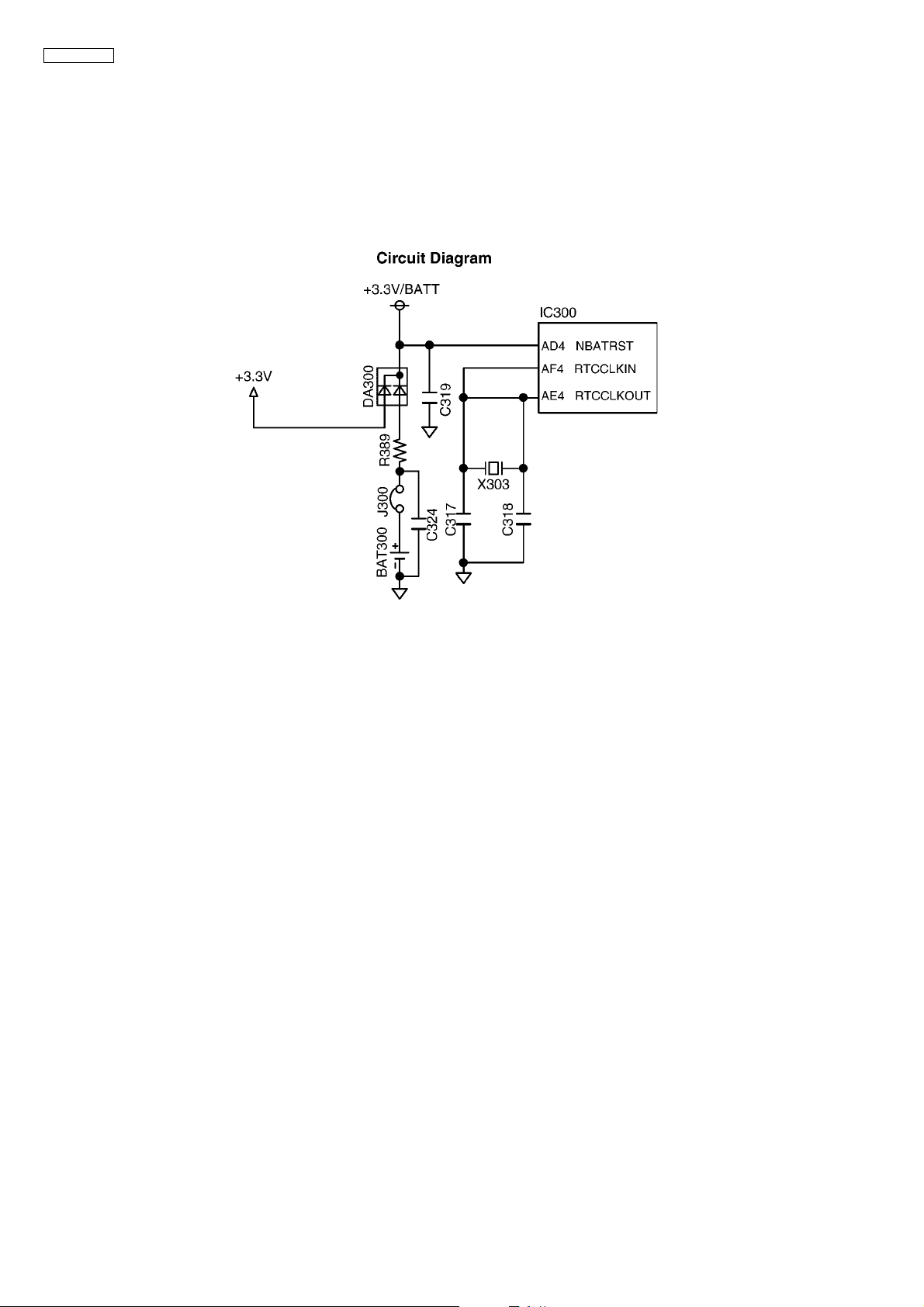
6.3.2. RTC BACKUP CIRCUIT
1. Function
This unit has a lithium battery (BAT300) which works for the Real Time Clock IC (RTC: inside IC300).
The RTC continues to work, backed up by a lithium battery even when the power switch is OFF.
2. RTC Inside (IC300) Backup Circuit Operation
When the power switch is turned ON, power is supplied to the RTC (inside IC300). At this time, the voltage at pin AD4 of the
IC300 is +3.3V . When the power switch is turned OFF, the BA T300 supplies power to RTC through DA300.
When the power switch is OFF and the voltage of +3.3V decreases, pin AD4 of RTC (IC300) becomes roughly the same voltage as the battery voltage. RTC goes into the backup mode, in which the power consumption is lower.
22
KX-MB283BR
6.4. CIS CONTROL SECTION
The scanning block of this device consists of a control circuit and a CIS (contact image sensor), and AFE (Analog Front End)
include A/D Converter.
When an original document is inserted and the start button pressed, pin A3 o f IC300 goes to a low level and the transistor Q51 8
turns on. This applies voltage to the CIS. The CIS is driven by e ach of the CCDSH , CCDCLK signals output from IC300, and the
original image illuminated by the LED to output an analog image signal.
The analog image signal is input to the AFE on VINP(20pin of IC503 ) and converted into 16-bit data by the A/D conve rter inside
IC503. Then this signal undergoes digital processing in order to obtain a high-quality image.
23
KX-MB283BR
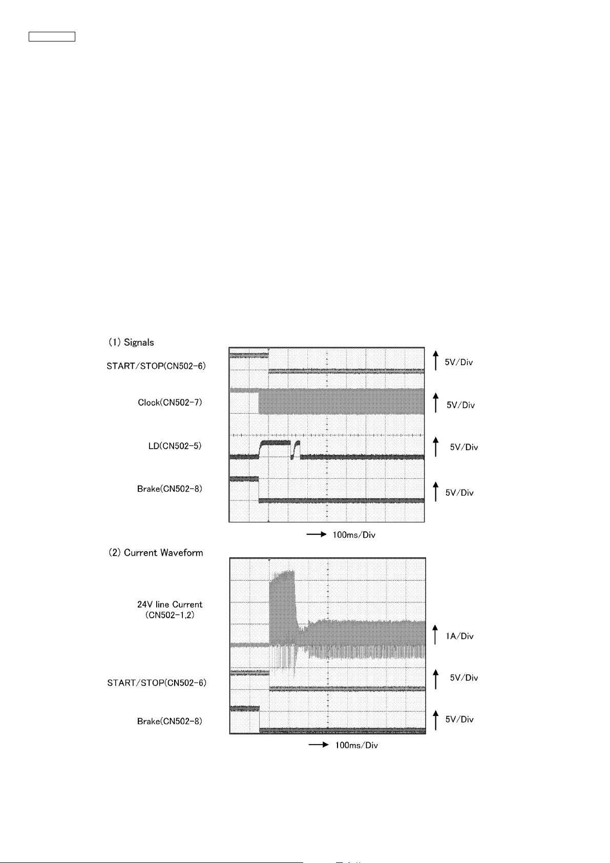
6.5. MOTOR DRIVE SECTION
6.5.1. Engine Motor Control Circuit
1. Functions
All driving forces of printer engine part are supplied by this engine motor.
Engine motor is controlled so as to rotate at constant speed during printing and copying.
2. Motor operation
<Start operation>
In order to start the motor rotation, following 3 signals are supplied from IC300.
1. SS signal (Output pin: Pin B12/Output Signal: "H")
When this signal is inverted by transistor Q502 and becomes "L", motor recognize this signal as "start" signal.
2. Clock signal (Output pin: Pin A12/Output Signal: Pulse)
Pulse frequency :approx. 1.9KHz (at normal printing speed, )
Pulse frequency :approx. 0.5KHz.(at half printing speed)
This signal is also inverted by transistor Q525, and supplied to motor as "clock" signal .
3. Brake signal (Output pin: Pin C12/Output Signal: "H")
When this signal is inverted by transistor Q526 and becomes "L", motor recognize this signal as "brake off" signal.
When motor reaches constant speed, "L" signal is supplied from motor to IC300 pin B12 as "Lock detect (LD)" signal.
if "LD" signal does not becomes "L" within predetermined period after "SS" signal becomes "H", or if "LD" signal becomes
"H" during rotation, it is judged that motor Error occurred.
Timing Chart of Start operation
24
KX-MB283BR
<Stop operation>
In order to stop the motor rotation, following 2 signals are supplied from IC300.
1. SS signal (Output pin: Pin B12/Output Signal: "L")
When this signal is inverted by transistor Q502 and becomes "H", motor recognize this signal as "stop" signal.
2. Brake signal (Output pin: Pin C12/Output Signal: "L")
When this signal is inverted by transistor Q526 and becomes "H", motor recognize this signal as "brake on" signal.
Timing Chart of Stop operation
6.5.1.1. ENGINE MOTOR DRIVE CIRCUIT
25
KX-MB283BR
6.5.2. SCANNER MOTOR DRIVE CIRCUIT
General
Scanner motor drive circuit is consist of motor current control circuit ,FB (Flat Bed) motor driver and ADF (Auto Document Feeder:
equipped model only) motor driver .
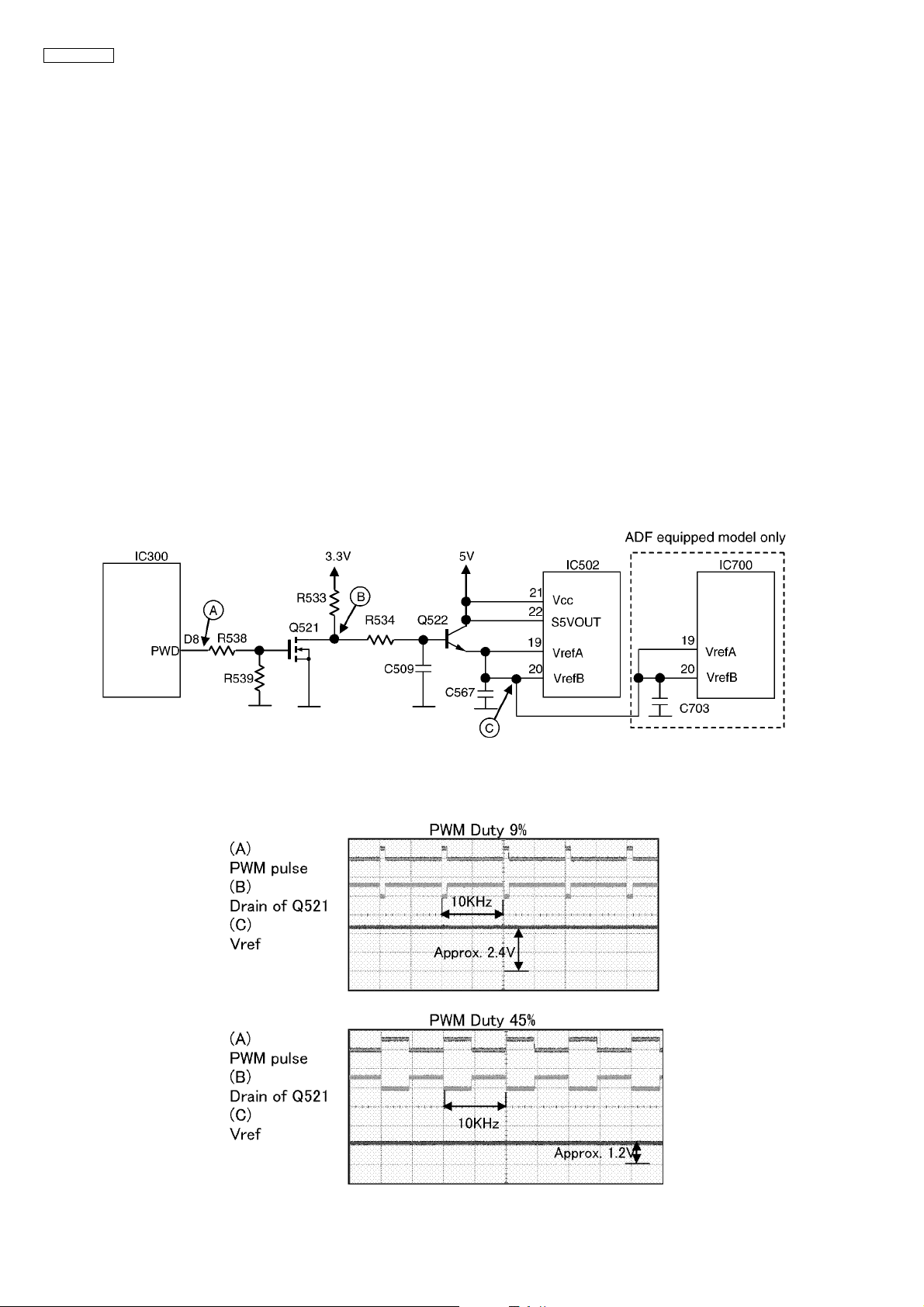
6.5.2.1. MOTOR CURRENT CONTROL CIRCUIT
1. Circuit explanation
According to the scan speed, each motor current is controlled for appropriate value.
When scan speed is low, motor current is reduced to prevent the vibration during motor rotation.
When scan speed is high, motor needs much driving force. so much current should be supplied.
For the control of motor current, Vref voltage of each motor driver is controlled.
When Vref voltage is high, motor current is increased, and the voltage is low, motor current is reduced.
In order to control Vref voltage, PWM pulse is supplied from IC300 pin D8 .
PWM pulse is inverted by Q521 and integrated by R533, R534, and C567, then convert to DC voltage.
This DC voltage is supplied to Vref pin of each motor driver through Q522.
When duty of PWM pulse is high, Vref voltage is decreased and when duty is low, Vref voltage is increased.
For FB motor, motor current is controlled approx. 0.1A-0.25A.
For ADF motor, motor current is controlled approx. 0.2A-0.35A (ADF epuipped model only).
2. Circuit diagram
3. Timing chart
Following timing charts are the example when PWM pulse duty are approx 9% and 45%.
26
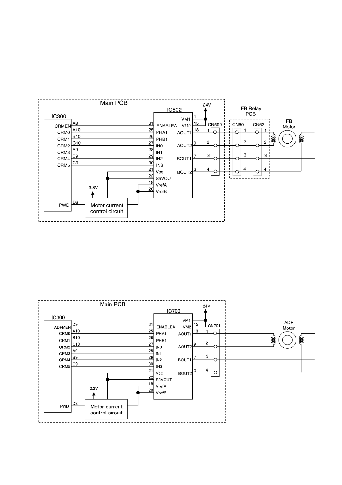
6.5.2.2. FB (FLAT BED) MOTOR DRIVE CIRCUIT
1. Functions
This motor functions for main operations including FB copy and PC scan.
This motor feeds CIS unit with synchronizing for reading.
2. Motor operation
During motor driving, pin A8 of IC 300 become low level, then motor driver IC502 is activated.
Stepping pulses are output from IC300 pins A9, B9, C9,A10, B10, and C10, causing driver IC502 pin 3, 7, 9 and 13 to dri ve
the motor coil.
A 1-step rotation of this motor feeds 0.021 mm of CIS unit.
3. Circuit Diagram
KX-MB283BR
6.5.2.3. ADF (AUTO DOCUMENT FEEDER) MOTOR DRIVE CIRCUIT
1. Functions
This motor functions for main operations including ADF copy and PC scan.
This motor feeds document which are set to ADF with synchronizing for reading.
2. Motor operation
During motor driving, pin D9 of IC 300 become low level, then motor driver IC700 is activated.
Stepping pulses are output from IC300 pins A9, B9, C9, A10, B10, and C10, causing driver IC700 pin 3, 7, 9 and 13 to dr ive
the motor coil.
A 1-step rotation of this motor feeds 0.04 2 mm of doc ument.
3. Circuit Diagram
27
KX-MB283BR
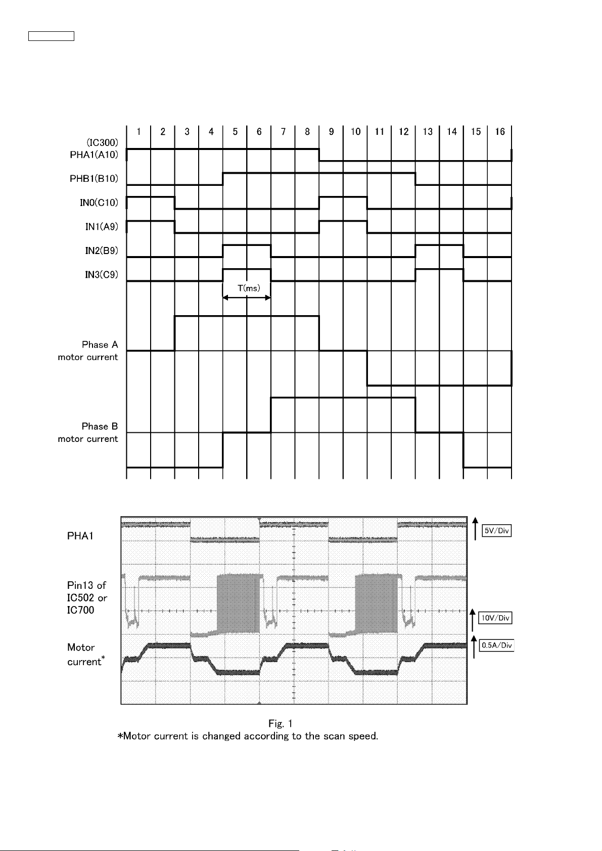
6.6. TIMING CHART AND WAVE FORM OF SCANNER MOTORS
Control sequence and waveform of both FB and ADF motor are almost same.
6.6.1. NORMAL 1-2 PHASE EXCIT ATION (HALF STEP)
1. Timing chart
2. Wave form
28
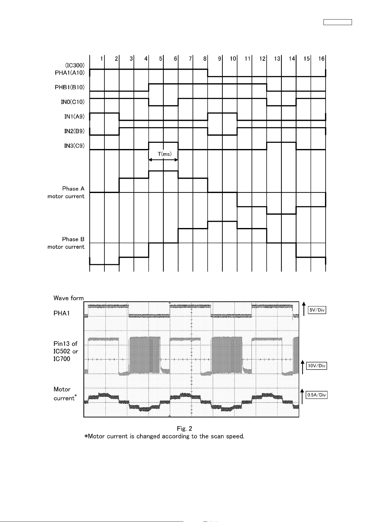
6.6.2. FLAT TORQUE 1-2 PHASE EXCITATION (HALF STEP)
1. Timing chart
KX-MB283BR
2. Wave form
29
KX-MB283BR
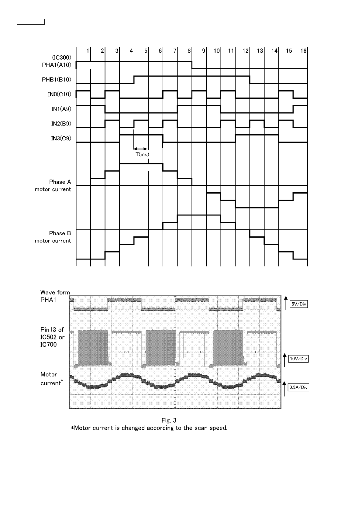
6.6.3. W 1-2 PHASE EXCITATION (QUARTER STEP)
1. Timing chart
2. Wave form
30
 Loading...