

Panasonic MN6761S Datasheet
For Video Equipment
MN6761S
External Synchronization Control LSI for Color Video Cameras
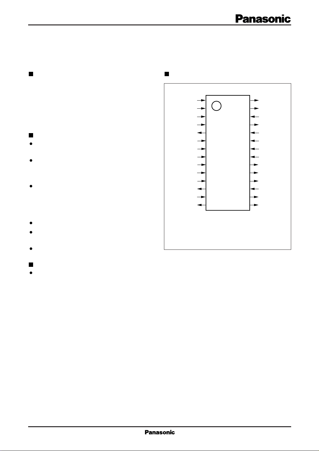
Pin Assignment Overview
The MN6761S is an external synchronization control
LSI for color video cameras.
When used in combination with a synchronizing signal
generator (MN67601NS or MN67602PS), it provides
external synchronization control for NTSC and PAL video
systems.
Features
Synchronization of both the video camera and the
VCR
External synchronization inputs:
Composite synchronizing signal and burst
subcarrier
External synchronization techniques
• Horizontal synchronization: phase-locked loop
• Vertical synchronization: reset technique
• Subcarrier synchronization: phase-locked loop
Support for both NTSC and PAL systems
Built-in feature for automatically switching between
external and internal synchronization
Built-in horizontal phase adjustment circuit
SCPSW1
SCPSW2
WHD
N/P
BGP
GLBSC
V
SS2
V
DD2
GLSYNC
TEST2
f
HPCO
XfHOSCI
XfHOSCO
HP
1
2
3
4
5
6
7
8
9
10
11
12
13
14
(TOP VIEW)
SOP028-P-0375
28
27
26
25
24
23
22
21
20
19
18
17
16
15
4f
4fSCOSCO
4fSCOSCI
SOPCO
SC1
V
V
TEST1
HBLK
EXT/INT
LSWCONT
LSW
VR
Xf
SC
DD1
SS1
H
Applications
Color video cameras
MN6761S For Video Equipment
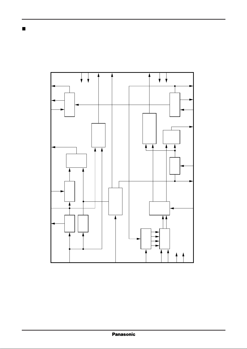
Block Diagram
Xf
Xf
OSCO
Xf
OSCI
HPCO
f
WHD
DD2VSS2
V
8
H
14
H
13
H
oscillator
H
Xf
12
Phase
com-
parator
11
HP
Monostable
multivibrator
7
Internal/external
EXT/INT
19
20
synchronization
switch
HBLK
3
HBLK and BGP
fH
pulse generator
DD1VSS1
V
LSWCONT
18
Line switch control
22
23
pulse generator
Line
Phase
switch
generator
SC
4f
com-
parator
Gate
2815
4f
SC
27
4f
SC
OSCO
26
4f
SC
OSCI
25
SCPCO
6
GLBSC
5
BGP
17
LSW
VR
fV
16
V
separation
H
separation
0˚
90˚
CK
Shift register
Selector
D
10
TEST2
SCPSW2
21
TEST1
9
GLSYNC
1
4
N/P
24
SC1
2
SCPSW1
For Video Equipment MN6761S
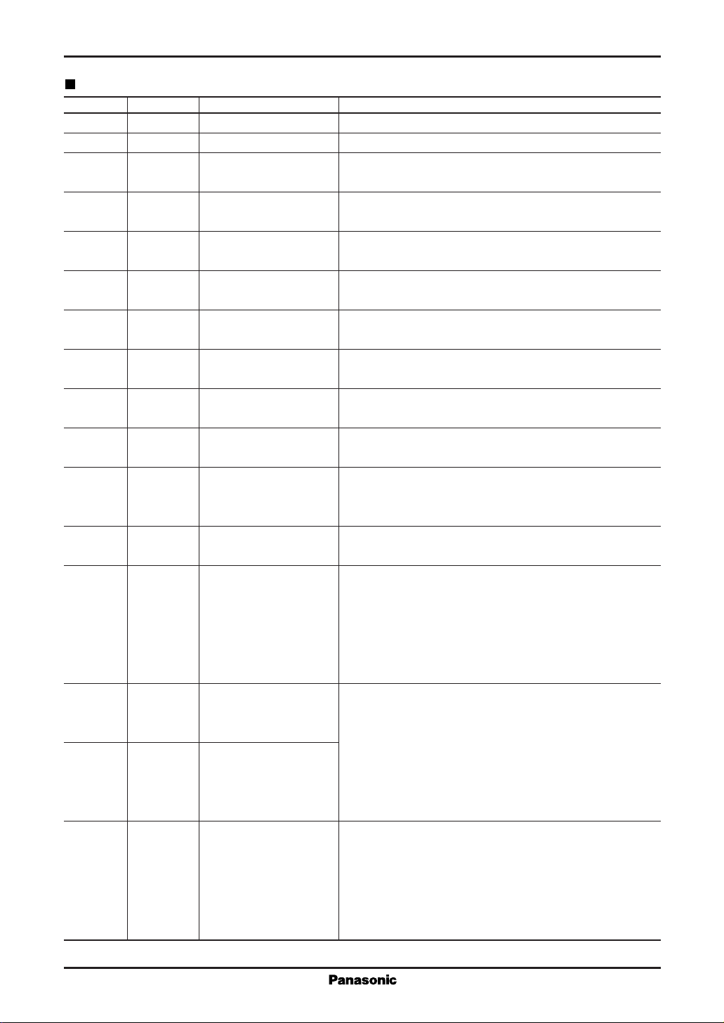
Pin Descriptions
Pin No. Symbol Pin Name Function Description
23 V
22 V
8V
7V
DD1
SS1
DD2
SS2
9 GLSYNC External synchronizing
6 CLBSC External burst
3 WHD Horizontal synchroni-
11 f
HP
24 SC1 Subcarrier input
1 SCPSW1 Subcarrier phase
2 SCPSW2 switch inputs
17 LSW Line switch input
4 N/P NTSC/PAL selection
12 HPCO Horizontal phase
13 XfHOSCI Oscillator input for
14 Xf
15 Xf
OSCO Oscillator output for
H
H
Power supply "H" level (5V) power supply for subcarrier circuits
Power supply "L" level (GND) power supply for subcarrier circuits
Power supply "H" level (5V) power supply for synchronizing signal
circuits
Power supply "L" level (GND) power supply for synchronizing signal
circuits
Input pin for composite synchronizing signal derived from
signal input
video signal (reference for horizontal and vertical signals)
Input pin for burst subcarrier signal derived from video
subcarrier input
signal (reference for subcarrier signals)
Input pin for WHD signal from synchronizing signal
zation input
Monostable multivibrator input
generator
Pin for connecting CR circuit for adjusting delay for analog
monostable multivibrator (thus adjusting horizontal phase)
Input pin for SC1 signal from synchronizing signal
generator
Pin selecting which of the four phase signals generated from
the SC1 signal goes to the phase comparator
For a PAL system, supply the LSW signal from the
synchronizing signal generator.
For an NTSC system, keep this pin at "H" level.
"H" level selects NTSC operation;
input
"L" level, PAL operation.
This pin is at "L" level when the WHD signal, after passing
comparator output
through the monostable multivibrator, leads the rising edge
of the HSYNC signal derived by separating off the
horizontal component of the GLSYNC signal and is at "H"
level when the signal lags. At all other times, it is in the
high-impedance state.
Clock oscillator pins for the synchronization circuits.
the synchronization
circuits
Connect these pins to an inductor, capacitor, and variable
capacitor. (The pins have built-in feedback resistors.)
The circuit oscillates during external synchronization mode.
the synchronization
circuits
Clock output for
synchronizing signal
circuits
The oscillation stops for internal synchronization mode.
The oscillator frequency, Xf
NTSC and 4.406 MHz (282f
is 14.31818 MHz (910fH) for
H
) for PAL.
H
Clock output pin for synchronizing signal circuits.
This pin provides the clock (Xf
) for the external
H
synchronization mode and stays at "L" level for the internal
synchronization mode. Connect to the EX910f
I pin of the
H
synchronizing signal generator for NTSC operation and to
the EX282f
I pin for PAL operation.
H
 Loading...