

Panasonic MN65771F Datasheet
A/D, D/C Converters for Image Signal Processing
MN65771F
Low Power 10-Bit 5 V CMOS A/D Conv erter for Image Processing
Overview
The MN65771F is a high-speed 10-bit CMOS analog-
to-digital converter for image processing applications.
It uses a half flash structure based on chopper comparators to achieve both high speed and low power consumption.
Features
Maximum conversion rate: 18 MSPS (min.)
Linearity error: ±1.3 LSB (typ.)
Differential linearity error: ±1.0 LSB (typ.)
Power supply voltage: 5.0 V or 3.3 V
Power consumption: 115 mW (typ.) (f
=20 MHz)
CLK
Applications
Digital television receivers
Digital video equipment
Digital image processing equipment
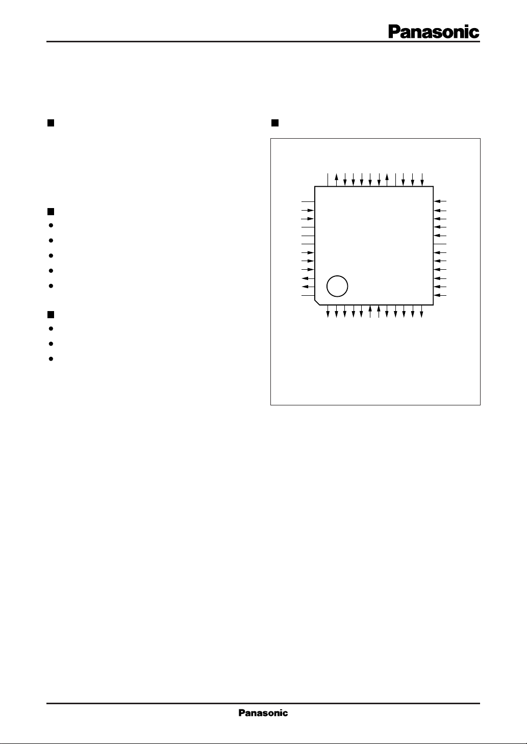
Pin Assignment
RBSVRBVR3VR2VR1VRTVRTS
N.C.
V
N.C.
AV
V
N.C.
N.C.
N.C.
AV
DV
DV
LINDF
OVF
N.C.
DD
IN
SS
SS
DD
3635343332313029282726
37
38
39
40
41
42
43
44
45
46
47
48
1234567891011
D0D1D2D3D4
N.C.
SS
D5D6D7D8D9
DDL
DV
DV
(TOP VIEW)
QFH048-P-0707
DD
AVSSAVDDAV
25
24
23
22
21
20
19
18
17
16
15
14
13
12
POWD
NOE
CLK
MINV
LINV
N.C.
DV
DD
DV
SS
DV
SS
DV
DD
TEST1
TEST2
1
MN65771F A/D, D/C Converters for Image Signal Processing
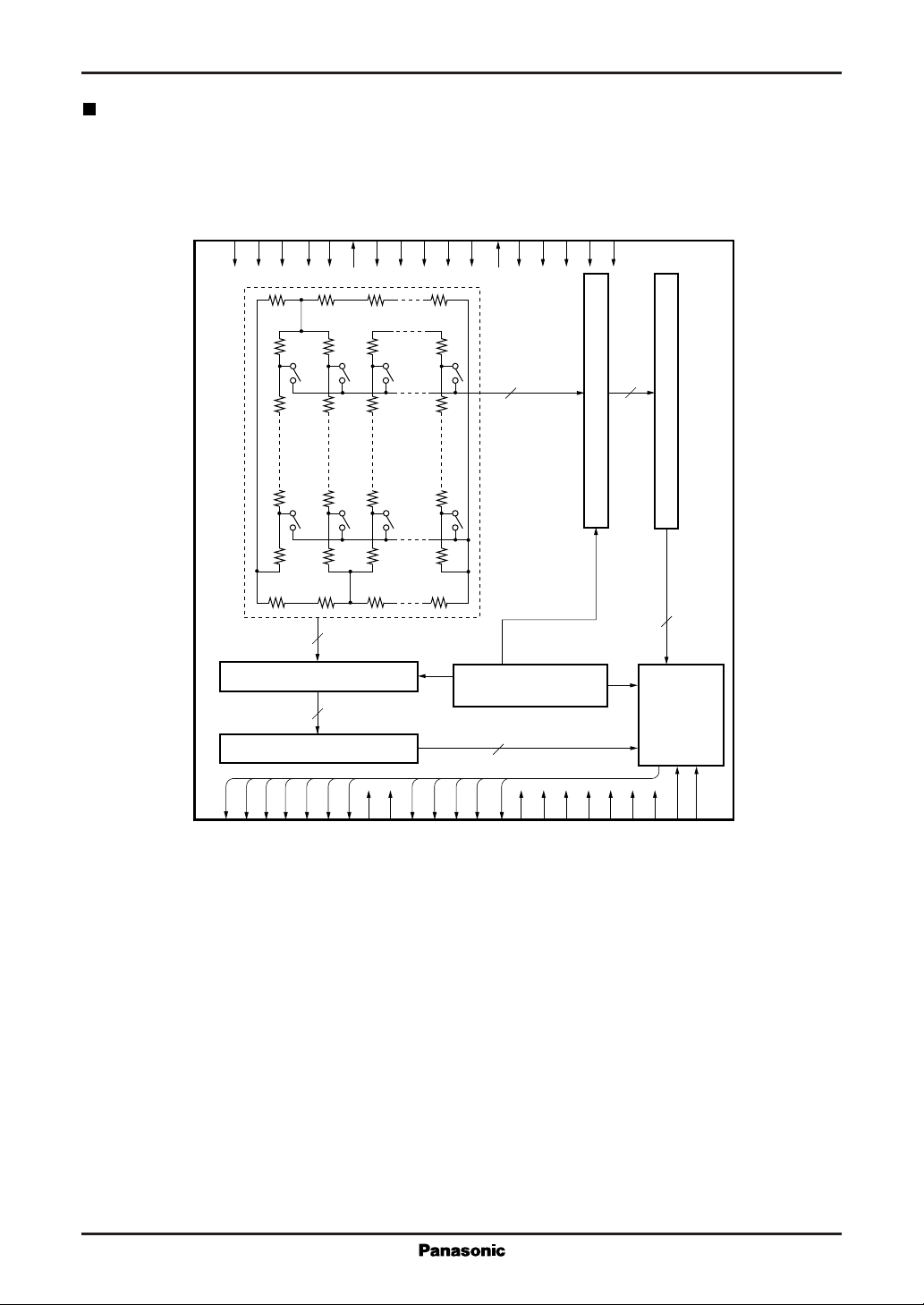
Block Diagram
SS
DVDDDV
45444339383534333231302927
AV
DD
SS
RBS
AV
RB
V
IN
V
31
RTS
V
VRTVR1VR2VR3V
29
DDAVSS
AV
AVDDLINV
262521
Pin NO.
19, 28, 36, 37,
( )
40, 41, 42, 48 are N.C.pin.
MINV
20
57
Lower comparator (5 bits)
Lower encoder (5 bits)
5
Upper comparator (5 bits)
31
Upper encoder (5 bits)
46
UNDF
47
OVF
123
(LSB)
D0
45678
D1
D2
D3
D4
SS
DV
DDL
DV
Clock generator
5
9
1011121314151617182223
TEST2
TEST1
DD
DV
DVSSDV
D5
D6D7D8
D9
SS
DV
Error
correction
and
data latch
DD
CLK
NOE
24
POWD
2
 Loading...