

Panasonic MN6570F, MN6570TF, MN6570EF Datasheet
A/D, D/C Converters for Image Signal Processing
MN6570F, MN6570TF, and MN6570EF
Low Power 8-Bit, 3-Channel CMOS D/A Converters for Image Processing
Overview
The MN6570F, MN6570TF, and MN6570EF are highspeed 8-bit, 3-channel CMOS digital-to-analog converters with maximum conversion rates of 35 MSPS, 40
MSPS, and 40 MSPS, respectively.
They use both a matrix cell and weighted current technology.
The three channels use separate clock signals, so they
may be used as totally independent D/A converters.
Features
Maximum conversion rate:
MN6570F: 35MSPS (min.)
MN6570TF and MN6570EF: 40 MSPS (min.)
Linearity error: ±0.2 LSB (typ.)
Differential linearity error: ±0.2 LSB (typ.)
Power supply voltage: VCC= 5.0±0.5 V
Power consumption:
MN6570F: 340 mW (typ.)
MN6570TF and MN6570EF: 190 mW (typ.)
Full scale current:
MN6570F: 13 mA (typ.)
MN6570TF and MN6570EF: 5 mA (typ.)
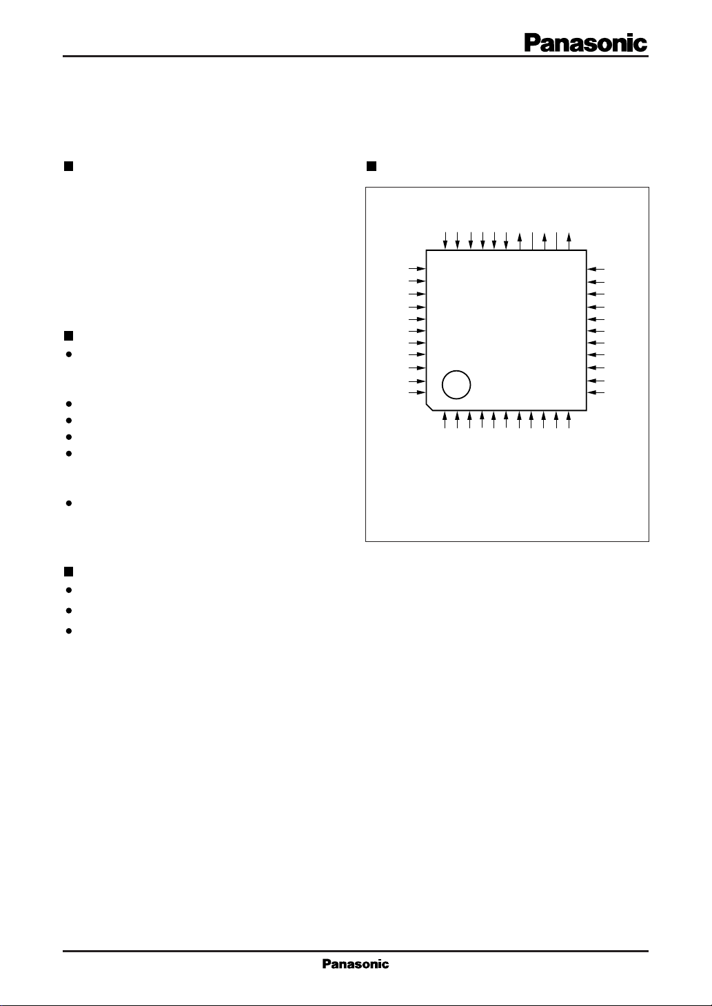
Pin Assignment
DB5
DB6
DB4
DB3
DB2
DB1
CLKB
DV
DV
DG8
DG7
DG6
DG5
SS
DD
3332313029282726252423
34
35
36
37
38
39
40
41
42
43
44
1234567891011
DG4
DG3
QFP044-P-1010
SSAVSS
DB7
DB8
AV
IOBN.C.
SS
DG1
DV
CLKG
DD
DV
DG2
(TOP VIEW)
DR8
IOGN.C.
DR7
DR6
OR
I
22
21
20
19
18
17
16
15
14
13
12
DR5
VIB
COMP
V
REF
I
REF
AV
DD
AV
DD
CLKR
DR1
DR2
DR3
DR4
Applications
Digital television
Digital video equipment
Digital image processing equipment
1
MN6570F, MN6570TF, MN6570EF
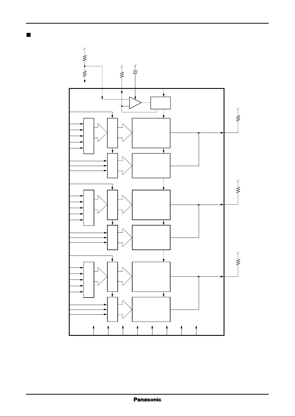
Block Diagram
A/D , D/C Conv erters for Image Signal Processing
CLKR
(MSB)DR1
DR2
DR3
DR4
DR5
DR6
DR7
(LSB)DR8
CLKG
(MSB)DG1
DG2
DG3
DG4
DG5
DG6
DG7
(LSB)DG8
R
REF
REF
V
20
REF
I
19
16
15
14
13
12
DecoderDecoder
–
COMP
21
+
–
C
COMP
Matrix
Cell
22
Current
Source
VIB
N.C.
24
N.C.
26
R
OUT
I
23
OR
11
+
10
9
8
Weighted
Current Cell
5
R
4
3
2
Matrix
Cell
I
25
OUT
OG
1
44
43
42
41
Weighted
Current Cell
38
CLKB
R
(MSB)DB1
DB2
DB3
DB4
DB5
DB6
DB7
(LSB)DB8
37
36
35
34
Decoder
Latch Latch Latch Latch LatchLatch
Matrix
Cell
I
27
33
32
31
30
17
18
28
DD
AVDDAV
AVSSAV
Weighted
Current Cell
29
SS
7
DVDDDV
6
40
DD
39
SS
DVSSDV
OUT
OB
2
A/D, D/C Converters for Image Signal Processing
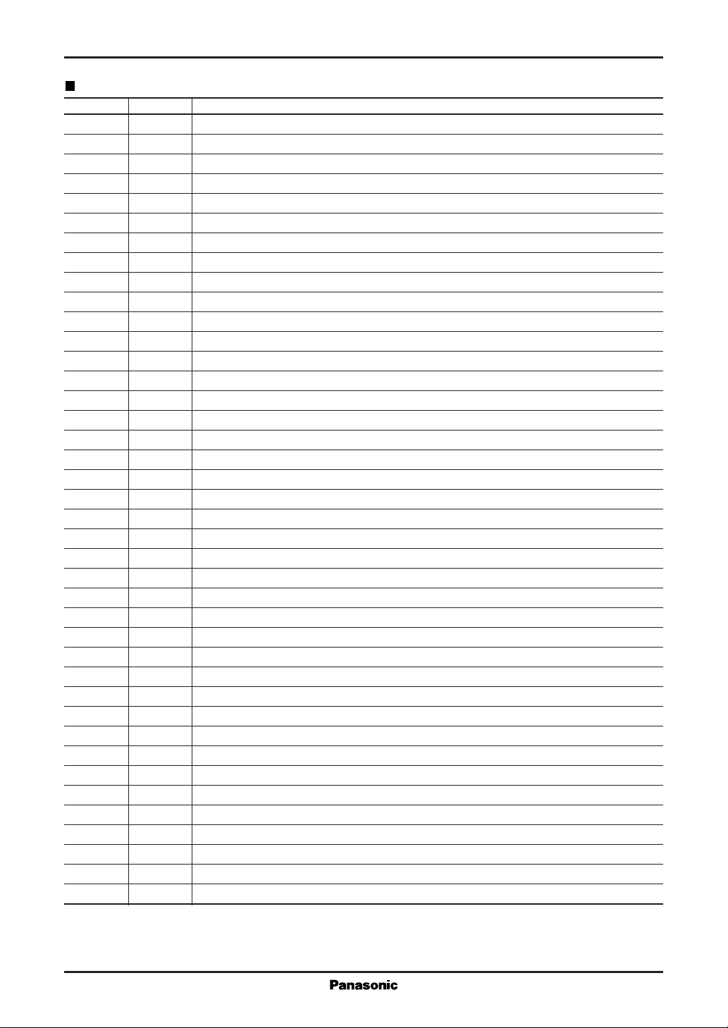
Pin Descriptions
Pin No. Symbol Function Description
1 DG4 G signal digital input
2 DG3 G signal digital input
3 DG2 G signal digital input
4 DG1 G signal digital input (MSB)
5 CLKG G signal sampling clock
6DVSSGround for digital circuits
7DVDDPower supply for digital circuits
8 DR8 R signal digital input (LSB)
9 DR7 R signal digital input
10 DR6 R signal digital input
11 DR5 R signal digital input
12 DR4 R signal digital input
13 DR3 R signal digital input
14 DR2 R signal digital input
15 DR1 R signal digital input (MSB)
16 CLKR R signal sampling clock
17 AV
18 AV
19 I
20 V
DD
DD
REF
REF
21 COMP Phase compensation
22 VIB Capacitor connection
23 I
OR
24 N.C. No connection
25 I
OG
26 N.C. No connection
27 I
28 AV
29 AV
OB
SS
SS
30 DB8 B signal digital input (LSB)
31 DB7 B signal digital input
32 DB6 B signal digital input
33 DB5 B signal digital input
34 DB4 B signal digital input
35 DB3 B signal digital input
36 DB2 B signal digital input
37 DB1 B signal digital input (MSB)
38 CLKB B signal sampling clock
39 DV
40 DV
SS
DD
Power supply for analog circuits
Power supply for analog circuits
Full scale adjustment resistor
Reference voltage input
R signal analog current output
G signal analog current output
B signal analog current output
Ground for analog circuits
Ground for analog circuits
Ground for digital circuits
Power supply for digital circuits
MN6570F, MN6570TF, MN6570EF
3
 Loading...