

Page 1
MN3300 Series
MN3304
512-Stage Ultra Low Voltage Operation BBD for Audio Signals
■ Overview
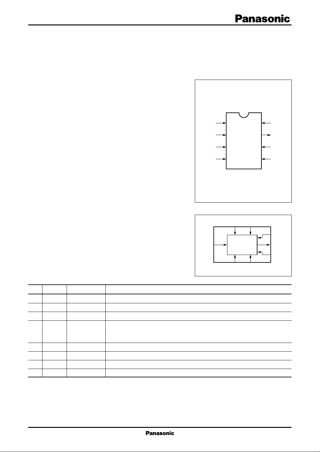
■ Pin Assignment
The MN3304 is a 512-stage ultra low voltage operation BBD variable
delay line in audio frequency range. The device operates on +3V
supply and provides a signal delay up to 25.6 ms and is suitable for
use as reverberation effect of low voltage operation audio equipment
such as portable stereo, radio cassette recorder and microphone.
■ Features
•
Variable signal delay of the audio signal : 0.256 to 25.6 ms
•
Wide range of supply voltage : 1.8 to 5.0 V
•
No insertion loss : L
•
Wide dynamic range : S/N=73 dB typ.
•
Low distortion : THD=0.7 % typ. (V
•
Clock frequency range :10 to 200 kHz (1.8 V≤V
•
N-channel 2-layer silicon gate process
•
8-Pin Dual-In-Line Plastic Package
=0 dB typ.
i
=0.22 V
i
10 kHz to 1 MHz (4.0 V≤V
rms
)
DD
<4.0 V)
DD
≤5.0 V)
GND
CP2
IN
V
DD
1
2
MN3304
3
4
DIP008-P-0300
V
8
OUT
7
CP1
6
V
5
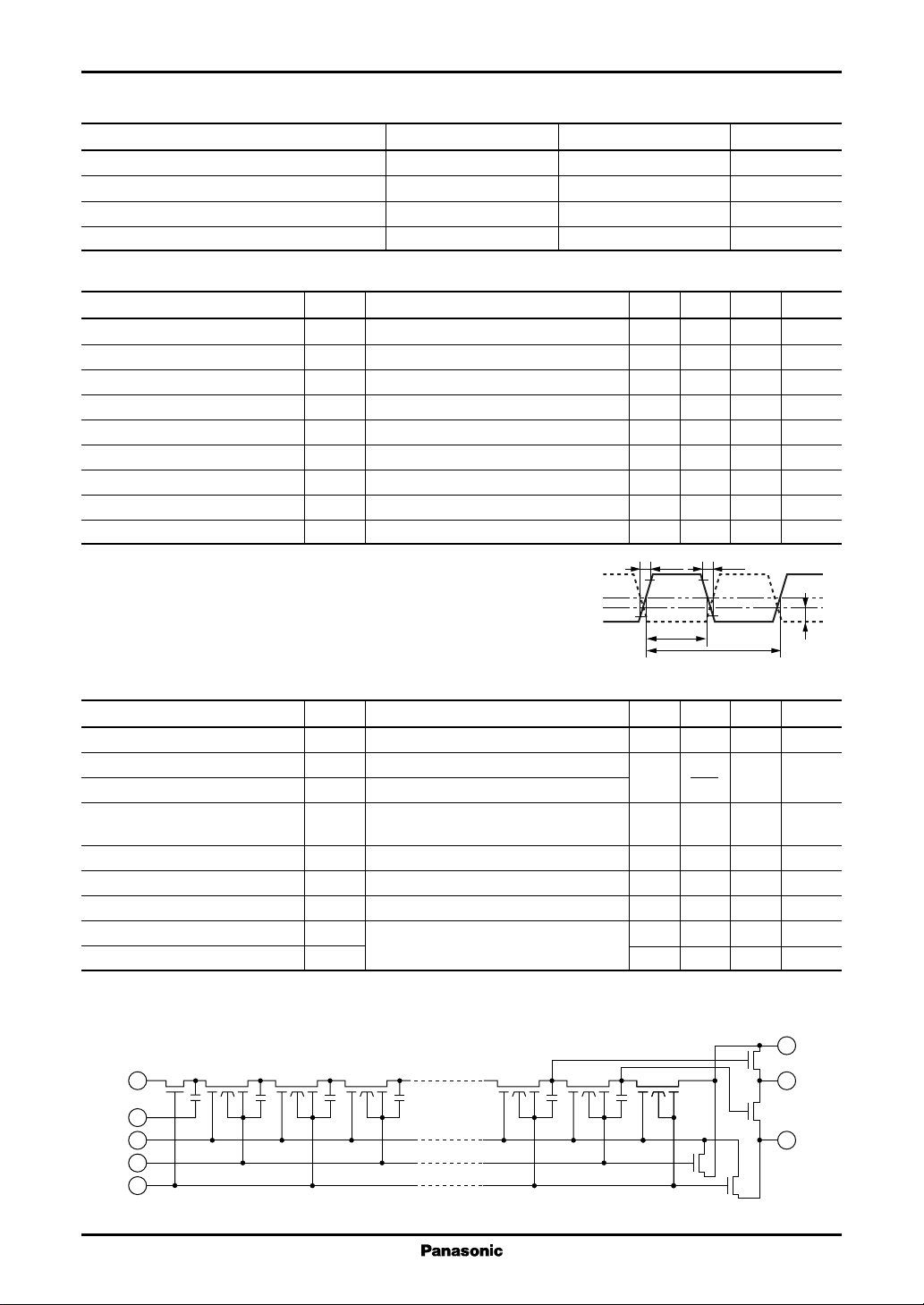
■ Block Diagram
■ Applications
•
Reverberation and echo effects of audio equipment such as radio
cassette recorder, car radio, portable radio, portable stereo, echo
microphone and Karaoke machine, etc.
•
Sound effect of electronic musical instruments
•
Variable or fixed delay of analog signals
IN
3
CP1
6
512-Stage
BBD
4
DD
V
CP2
2
1
GND
8
V
7
OUT
5
V
■ Pin Descriptions
Pin No.
Symbol Pin Name Description
1 GND Ground pin Connected to ground.
2 CP2 Clock input 2 Basic clock pulse is applied to transfer electric charge of BBD.
3 IN Signal input pin Analog signal to be delayed is input. Most suitable DC bias should be applied to this pin.
4VDDVDD apply pin Bias is applied to the gate of MOS transistor which is inserted in series with clock pulse
input gate of the BBD transfer gate.
Furthermore, voltage is supplied to step-up circuit.
5VD1VD1 apply pin The same phase clock pulse as CP1 is applied through capacitor.
6 CP1 Clock input 1 Clock pulse of inverted phase to CP2 is applied.
7 OUT Output pin Composed signal of 1024th and 1025th stages is output.
8VD2VD2 apply pin The same phase clock pulse as CP2 is applied through capacitor.
D2
D1
D2
D1
1
Page 2
MN3304 MN3300 Series
■ Absolute Maximum Ratings Ta=25°C
Parameter Symbol Ratings Unit
Pin voltage VDD, VD1, VD2, VCP, V
Output voltage V
Operating ambient temperature T
Storage temperature T
O
opr
stg
■ Operating Conditions Ta=25°C
Parameter Symbol Conditions min typ max Unit
Supply voltage V
Clock voltage "H"level V
Clock voltage "L"level V
Clock input capacitance C
Clock frequency f
Clock pulse width t
Clock rise time t
Clock fall time t
Clock cross point V
Note) *1: ( ) : VDD=4.0 to 5.0 V
*2:T=1/fCP (Clock period)
CPH
CPL
CP
w(CP)
r(CP)
f(CP)
DD
CP
3
*
3
*
3
*
3
*
X
*3: Clock pulse waveforms
I
− 0.3 to +6.0 V
− 0.3 to +6.0 V
−20 to +60 °C
−55 to +125 °C
+1.8 +3.0 +5.0 V
V
DD
0V
10
0 0.3V
t
CP2
CP1
r(CP)
90%
50%
10%
t
w(CP)
T
400 pF
200(1000)
0.5T
500 ns
500 ns
CPH
t
f(CP)
V
1
*
kHz
2
*
V
3V
V
X
■ Electrical Characteristics VDD=V
CPH
=3V, V
=0V, RL=56kΩ, LPF : fC=20kHz, Att=48dB/oct., Ta=25°C
CPL
Parameter Symbol Conditions min typ max Unit
Supply current I
Signal delay time 1 t
Signal delay time 2 t
Input signal frequency f
DDfCP
D1
D2
i
=40 kHz 0.05 mA
VDD=1.8 to 4.0 V, fCP=10 to 200 kHz N
VDD=4.0 to 5.0 V, fCP=10 kHz to 1 MHz 2·f
fCP=40 kHz, Vi=0.22 V
rms
12 kHz
*
CP
Output attenuation≤3 dB(0 dB at fi=1 kHz)
Input signal amplitude υ
Insertion loss L
Total harmonic distortion THD fCP=40 kHz, fi=1 kHz, Vi=0.22 V
Output noise voltage V
fCP=40 kHz, fi=1 kHz, THD=2.5 % 0.32 0.5 V
i
fCP=40 kHz, fi=1 kHz, Vi=0.22 V
i
nofCP
=100 kHz, Weighted by "A"curve 0.098 0.2 mV
rms
rms
−40 4 dB
0.7 2.5 %
Signal to noise ratio S/N 73 dB
Note) * : N=BBD stages
■ Circuit Diagram
8V
513512321
7 OUT
5V
GND
V
CP1
CP2
3IN
1
4
DD
6
2
ms
rms
rms
D2
D1
2
Page 3

MN3300 Series MN3304
■ Typical Characteristics
6
5
(V)
O
4
3
2
DC output voltage V
1
0
01
VO V
DC input voltage V
−100
−90
(dBm)
−80
no
−70
−60
−50
Output noise voltage V
−40
20 40
Vno f
60 80 100 120 160 180140
Clock frequency f
I
=3V
V
DD
f
=40kHz
CP
Ta=25°C
234
(V)
I
CP
=3V
V
DD
Ta=25°C
(
)
kHz
CP
20
10
(dBm)
0
o
−10
−20
Output signal level V
−30
−40
−40 −30
Vo V
−20 −10 100
Input signal level V
Gi f
4
2
(dB)
i
0
−2
Insertion gain G
−4
−6
0.1
10kHz
0.3 1 3 30 10010
Input frequency f
i
V
f
CP
f
=1kHz
i
Ta=25°C
(
i
i
fCP=100kHz
40kHz
(
kHz
i
=3V
DD
=40kHz
dBm
=3V
V
DD
Ta=25°C
)
6
5
(%)
4
3
2
1
Total harmonic distortion THD
0
−20 −15
)
10
5
(dB)
i
0
−5
Insertion gain G
−10
−15
−20
THD V
−10 −550
Input signal level V
Gi V
−15 −10 −55100
Input signal level V
i
i
i
V
DD
f
CP
f
=1kHz
i
Ta=25°C
(
dBm
V
DD
f
=1kHz
i
f
CP
Ta=25°C
(
dBm
i
=3V
=40kHz
)
=3V
=40kHz
)
5
4
3
2
(dB)
i
1
0
−1
−2
Insertion gain G
−3
−4
−5
1
3 10 30 300 1000100
Clock frequency f
Gi f
CP
=3V
V
DD
f
=1kHz
i
Ta=25°C
(
)
kHz
CP
6
5
(%)
4
3
2
1
Total harmonic distortion THD
0
1.0
THD V
1.2 1.4 1.6 2.0 2.21.8
Input bias voltage V
Bias
V
f
=1kHz
i
f
CP
V
Ta=25°C
Bias
=3V
DD
=40kHz
=0.22V
i
(V
3
rms
)
2
1
(dB)
i
0
−1
−2
Insertion gain G
−3
−4
−5
−40
Ambient temperature Ta
Gi Ta
−20 0 20 100 1206040 80
V
DD
=1kHz
f
i
f
CP
=3V
=40kHz
(°C)
3
Page 4

MN3304 MN3300 Series
■ Typical Characteristics (To be continued)
V
1
0
−1
(dBm)
−2
i(max)
−3
i(max)
Ta
=3V
V
DD
f
=40kHz
CP
=1kHz
f
i
THD=2.5%
40
30
(kHz)
i
20
=3V
V
DD
=40kHz
f
CP
)=Vo(1kHz)−3dB
V
o(fi
(%)
1.6
1.4
1.2
1.0
0.8
THD Tafi Ta
=3V
V
DD
f
=1kHz
i
=40kHz
f
CP
V
=0.22V
i
rms
−4
−5
Input signal level V
−6
−7
−20 0 20 100 1206040 80
−40
Ambient temperature Ta
(°C)
■ Supply Voltage Characteristics
V
V
6
5
(V)
4
Bias
3
2
Input bias voltage V
1
0
0
Bias
24 86
Supply voltage V
DD
DD
Ta=25°C
(V)
10
Input frequency f
0
−20 0 20 100 1206040 80
−40
Ambient temperature Ta
(%)
4
THD V
3
2
1
DD
f
=40kHz
CP
f
=1kHz
i
V
i=Vi(max)
Ta=25°C
Total harmonic distortion THD
0
0
2846
Supply voltage V
DD
0.6
0.4
0.2
Total harmonic distortion THD
0
−20 0 20 100 1206040 80
−40
Ambient temperature Ta
22
20
(kHz)
18
i
16
14
f
V
i
fCP=40kHz
V
Ta=25°C
o(fi
(°C)
DD
)=Vo(1kHz)−3dB
−6dB
(°C)
Input frequency f
12
10
(V)
024 86
Supply voltage V
(V)
DD
20
10
(dBm)
i(max)
0
−10
Input signal level V
−20
0
Supply voltage V
4
V
V
i(max)
2846
DD
f
=40kHz
CP
f
=1kHz
i
THD=2.5%
Ta=25°C
(V)
DD
4
3
2
(dB)
i
1
0
−1
Insertion gain G
−2
−3
−4
0
2846
Supply voltage V
Gi V
DD
f
=40kHz
CP
f
=1kHz
i
V
i=Vi(max)
Ta=25°C
DD
110
S/N V
−6dB
(V)
100
(dB)
90
80
70
Signal to noise ratio S/N
60
50
024 86
Supply voltage V
DD
DD
Ta=25°C
(V)
Page 5

MN3300 Series MN3304
■ Package Dimensions (Unit : mm)
•
DIP008-P-0300
9.6±0.4
85
6.4±0.2
14
3.3±0.2
4.8max.
2.54
0.5±0.1
1.3±0.1
0.7min.
3.45±0.30
0 to 15˚
SEATING PLANE
7.62±0.20
0.25
+0.20
–0.05
5
 Loading...