

Page 1

MICROCOMPUTER MN1030
MN103001G/F01K
LSI User’ s Manual
Pub.No.23101-050E
Page 2

Page 3

PanaX Series is a trademark of Matsushita Electric Industrial Co., Ltd.
The other corporation names, logotype and product names written in this book are trademarks or registered trademarks of their
corresponding corporations.
Request for your special attention and precautions in using the technical
informaition and semiconductors described in this book
(1) An export permit needs to be obtained from the competent authorities of the Japanese Government if any of
the products or technologies described in this book and controlled under the "Foreign Exchange and Foreign
Trade Law" is to be exported or taken out of Japan.
(2) The contents of this book are subject to change without notice in matters of improved function.When
finalizing your design, therefore, ask for the most up-to-date version in advance in order to check for any
changes.
(3) We are not liable for any damage arising out of the use of the contents of this book, or for any infringement
of patents or any other rights owned by a third party.
(4) No part of this book may be reprinted or reproduced by any means without written permission from our
company.
(5) This book deals with standard specification. Ask for the latest individual Product Standards or Specifications
in advance for more detailsd infomation required for your design, purchasing and applications.
If you have any inquiries or questions about this book or our semiconductors, please contact one of our sales
offices listed at the back of this book.
Page 4

Page 5

Table of Contents/List of Figures and Tables
0
1. General Specifications
2. CPU
3. Extension Instruction Specifications
4. Memory Modes
5. Operating Mode
6. Clock Generator
1
2
3
4
5
6
7. Internal Memory
8. Bus Controller (BC)
9. Interrupt Controller
10. 8-bit Timers
11. 16-bit Timers
12. Watchdog Timer
7
8
9
10
11
12
13. Serial Interface
13
Page 6

Page 7

14. A/D Converter
14
15. I/O Ports
16. Internal Flash Memory
17. Ordering Mask ROM
Appendix
15
16
17
Page 8

Page 9

Table of Contents/List of Figures and Tables
0
Page 10

Table of Contents
1. General Specifications
1.1 Overview........................................................................................................................ 1-2
1.2 Features .......................................................................................................................... 1-2
1.3 Block Diagram ............................................................................................................... 1-4
1.4 Pin Description............................................................................................................... 1-5
1.4.1 Pin Assignments............................................................................................ 1-5
1.4.2 Pin Functions ................................................................................................ 1-7
2. CPU
2.1 Basic Specifications of CPU .......................................................................................... 2-2
2.2 Block Diagram ............................................................................................................... 2-3
2.3 Programming Model ...................................................................................................... 2-4
2.3.1 CPU Registers ............................................................................................... 2-4
2.3.2 Control Registers .......................................................................................... 2-7
2.4 Instructions................................................................................................................... 2-10
2.4.1 Addressing Modes ...................................................................................... 2-10
2.4.2 Data Types .................................................................................................. 2-11
2.4.3 Instruction Set ............................................................................................. 2-12
2.5 Interrupts ...................................................................................................................... 2-14
2.5.1 Overview of Interrupts ................................................................................ 2-14
2.5.2 Registers...................................................................................................... 2-15
2.5.3 Interrupt Types............................................................................................ 2-18
2.5.4 Interrupt Definition ..................................................................................... 2-19
3. Extension Instruction Specifications
3.1 Operation Extension Function ....................................................................................... 3-2
3.2 Extension Instructions.................................................................................................... 3-3
3.2.1 Explanation of Notations .............................................................................. 3-3
3.2.2 Extension Block Register Set........................................................................ 3-4
3.2.3 Extension Instruction Details ........................................................................ 3-5
3.2.4 Programming Notes .................................................................................... 3-31
4. Memory Modes
4.1 Memory Mode Types and Selection .............................................................................. 4-2
4.2 Memory Mode Pin Processing....................................................................................... 4-3
4.3 Description of Memory Mode ....................................................................................... 4-4
4.3.1 Memory Extension Mode ............................................................................. 4-4
4.3.2 Processor Mode............................................................................................. 4-5
ii
Page 11

5. Operating Mode
5.1 Overview........................................................................................................................ 5-2
5.2 Reset Mode .................................................................................................................... 5-3
5.3 Low Power Mode........................................................................................................... 5-4
6. Clock Generator
6.1 Overview........................................................................................................................ 6-2
6.2 Features .......................................................................................................................... 6-2
6.3 Block Diagram ............................................................................................................... 6-2
6.4 Description of Operation................................................................................................ 6-3
6.4.1 Input Frequency Setting ................................................................................ 6-3
6.4.2 Internal Clock Supply ................................................................................... 6-3
7. Internal Memory
7.1 Overview........................................................................................................................ 7-2
7.2 Features .......................................................................................................................... 7-2
7.3 Internal Memory Configuration ..................................................................................... 7-3
8. Bus Controller (BC)
8.1 Overview........................................................................................................................ 8-2
8.2 Features .......................................................................................................................... 8-2
8.3 Bus Configuration .......................................................................................................... 8-3
8.4 Block Diagram ............................................................................................................... 8-3
8.5 Pin Functions ................................................................................................................. 8-5
8.6 Description of Registers................................................................................................. 8-7
8.6.1 Memory Block 0 Control Register................................................................ 8-8
8.6.2 Memory Block 1 Control Register.............................................................. 8-10
8.6.3 Memory Block 2 Control Register.............................................................. 8-14
8.6.4 Memory Block 3 Control Register.............................................................. 8-19
8.6.5 DRAM control register ............................................................................... 8-22
8.6.6 Refresh count register ................................................................................. 8-23
8.6.7 Page Row Address Register........................................................................ 8-24
8.6.8 Clock Control Register ............................................................................... 8-24
8.7 Space Partitioning ........................................................................................................ 8-26
8.8 Operation Clocks ......................................................................................................... 8-28
8.9 Mode Settings .............................................................................................................. 8-28
8.10 Bus Cycle ..................................................................................................................... 8-29
8.11 Store Buffer.................................................................................................................. 8-30
8.12 Accessing the Internal I/O Space ................................................................................. 8-31
8.13 External Memory Space Access
(Non-DRAM Spaces).................................................................................... 8-32
8.13.1 16-bit Bus with Fixed Wait States, in Synchronous Mode
and in Address/Data Separate Mode........................................................... 8-33
iii
Page 12

8.13.2 16-bit Bus with Handshaking, in Synchronous Mode and in
Address/Data Separate Mode...................................................................... 8-35
8.13.3 16-bit Bus in Asynchronous Mode and in Address/Data
Separate Mode ............................................................................................ 8-37
8.13.4 8-bit Bus with Fixed Wait States, in Synchronous Mode
and in Address/Data Separate Mode........................................................... 8-39
8.13.5 8-bit Bus with Handshaking, in Synchronous Mode and in
Address/Data Separate Mode...................................................................... 8-41
8.13.6 8-bit Bus in Asynchronous Mode and in Address/Data
Separate Mode ............................................................................................ 8-45
8.13.7 16-bit Bus with Fixed Wait States, in Synchronous Mode
and in Address/Data Multiplex Mode......................................................... 8-46
8.13.8 16-bit Bus with Handshaking, in Synchronous Mode and
in Address/Data Multiplex Mode................................................................ 8-48
8.13.9 16-bit Bus in Asynchronous Mode and in Address/Data
Multiplex Mode .......................................................................................... 8-51
8.13.10 8-bit Bus with Fixed Wait States, in Synchronous Mode
and in Address/Data Multiplex Mode......................................................... 8-52
8.13.11 8-bit Bus with Handshaking, in Synchronous Mode and in
Address/Data Multiplex Mode.................................................................... 8-56
8.13.12 8-bit Bus in Asynchronous Mode and in Address/Data
Multiplex Mode .......................................................................................... 8-60
8.14 External Memory Space Access (DRAM Space) ........................................................ 8-62
8.14.1 DRAM Space .............................................................................................. 8-62
8.14.2 DRAM page mode ...................................................................................... 8-65
8.14.3 Software Page Mode ................................................................................... 8-66
8.14.4 DRAM refresh ............................................................................................ 8-68
8.15 Bus Arbitration.............................................................................................................8-70
8.16 Cautions ....................................................................................................................... 8-73
9. Interrupt Controller
9.1 Overview........................................................................................................................ 9-2
9.2 Features .......................................................................................................................... 9-2
9.3 System Diagram............................................................................................................. 9-2
9.4 Block Diagram ............................................................................................................... 9-3
9.5 Description of Registers................................................................................................. 9-6
9.6 Description of Operation.............................................................................................. 9-30
10. 8-bit Timers
10.1 Overview...................................................................................................................... 10-2
10.2 Features ........................................................................................................................ 10-2
10.3 Block Diagram ............................................................................................................. 10-3
10.4 Functions...................................................................................................................... 10-9
10.5 Description of Registers............................................................................................. 10-10
iv
Page 13

10.6 Description of Operation............................................................................................ 10-20
10.6.1 Interval Timers and Timer Output ............................................................ 10-20
10.6.2 Event Counting ......................................................................................... 10-24
10.6.3 Cascaded Connection................................................................................ 10-26
10.6.4 PWM Output ............................................................................................. 10-31
11. 16-bit Timers
11.1 Overview...................................................................................................................... 11-2
11.2 Features ........................................................................................................................ 11-2
11.3 Block Diagram ............................................................................................................. 11-3
11.4 Functions...................................................................................................................... 11-7
11.5 Description of Registers............................................................................................... 11-8
11.6 Description of Operation of Timer 10 ....................................................................... 11-18
11.6.1 Compare Register Settings........................................................................ 11-18
11.6.2 Capture Register Settings.......................................................................... 11-19
11.6.3 Pin Output Settings ................................................................................... 11-21
11.6.4 Starting by an External Trigger................................................................. 11-24
11.6.5 One-shot Operation ................................................................................... 11-26
11.6.6 Interval Timer ........................................................................................... 11-28
11.6.7 Event Counting ......................................................................................... 11-31
11.7 Description of Operation of Timers 11, 12 and 13 .................................................... 11-33
11.7.1 Interval Timer and Timer Output.............................................................. 11-33
11.7.2 Event Counting ......................................................................................... 11-36
12. Watchdog Timer
12.1 Overview...................................................................................................................... 12-2
12.2 Features ........................................................................................................................ 12-2
12.3 Block Diagram ............................................................................................................. 12-3
12.4 Description of Registers............................................................................................... 12-4
12.5 Description of Operation.............................................................................................. 12-7
13. Serial Interface
13.1 Overview...................................................................................................................... 13-2
13.2 General-purpose serial interface .................................................................................. 13-3
13.2.1 Features ....................................................................................................... 13-3
13.2.2 Block Diagram of General-Purpose Serial Interface .................................. 13-5
13.2.3 Description of Registers for the General-Purpose Serial Interface............. 13-6
13.2.4 Description of Operation........................................................................... 13-10
13.3 Clock Synchronous Serial Interface........................................................................... 13-24
13.3.1 Features ..................................................................................................... 13-24
13.3.2 Block Diagram of Clock Synchronous Serial Interface............................ 13-25
13.3.3 Description of Registers for the Clock Synchronous Serial Interface ...... 13-26
13.3.4 Description of Operation........................................................................... 13-32
13.4 Universal Asynchronous Receiver-Transceiver Serial Interface ............................... 13-36
13.4.1 Features ..................................................................................................... 13-36
v
Page 14

13.4.2 Block Diagram of UART Serial Interface ................................................ 13-37
13.4.3 Description of Registers for the UART Serial Interface........................... 13-38
13.4.4 Description of Operation........................................................................... 13-45
14. A/D Converter
14.1 Overview...................................................................................................................... 14-2
14.2 Features ........................................................................................................................ 14-3
14.3 Block Diagram ............................................................................................................. 14-4
14.4 Description of Registers............................................................................................... 14-5
14.5 Description of Operation.............................................................................................. 14-7
15. I/O Ports
15.1 Overview...................................................................................................................... 15-2
15.2 Port 0 ............................................................................................................................ 15-6
15.2.1 Block Diagram ............................................................................................ 15-6
15.2.2 Register Descriptions .................................................................................. 15-7
15.2.3 Pin Configuration........................................................................................ 15-9
15.3 Port 1 .......................................................................................................................... 15-10
15.3.1 Block Diagram .......................................................................................... 15-10
15.3.2 Register Descriptions ................................................................................ 15-12
15.3.3 Pin Configuration...................................................................................... 15-14
15.4 Port 2 .......................................................................................................................... 15-15
15.4.1 Block Diagram .......................................................................................... 15-15
15.4.2 Register Descriptions ................................................................................ 15-16
15.4.3 Pin Configuration...................................................................................... 15-18
15.5 Port 3 .......................................................................................................................... 15-19
15.5.1 Block Diagram .......................................................................................... 15-19
15.5.2 Register Descriptions ................................................................................ 15-20
15.5.3 Pin Configurations .................................................................................... 15-21
15.6 Port 4 .......................................................................................................................... 15-22
15.6.1 Block Diagram .......................................................................................... 15-22
15.6.2 Register Descriptions ................................................................................ 15-25
15.6.3 Pin Configurations .................................................................................... 15-28
15.7 Port 5 .......................................................................................................................... 15-29
15.7.1 Block Diagram .......................................................................................... 15-29
15.7.2 Register Descriptions ................................................................................ 15-34
15.7.3 Pin Configurations .................................................................................... 15-37
15.8 Port 6 .......................................................................................................................... 15-38
15.8.1 Block Diagram .......................................................................................... 15-38
15.8.2 Register Descriptions ................................................................................ 15-39
15.8.3 Pin Configurations .................................................................................... 15-40
15.9 Port 7 .......................................................................................................................... 15-41
15.9.1 Block Diagram .......................................................................................... 15-41
15.9.2 Register Descriptions ................................................................................ 15-42
vi
Page 15

15.9.3 Pin Configurations .................................................................................... 15-44
15.10 Port 8 .......................................................................................................................... 15-45
15.10.1 Block Diagram .......................................................................................... 15-45
15.10.2 Register Descriptions ................................................................................ 15-46
15.10.3 Pin Configurations .................................................................................... 15-47
15.11 Port 9 .......................................................................................................................... 15-48
15.11.1 Block Diagram .......................................................................................... 15-48
15.11.2 Register Descriptions ................................................................................ 15-50
15.11.3 Pin Configurations .................................................................................... 15-52
15.12 Port A ......................................................................................................................... 15-53
15.12.1 Block Diagram .......................................................................................... 15-53
15.12.2 Register Descriptions ................................................................................ 15-54
15.12.3 Pin Configurations .................................................................................... 15-56
15.13 Port B ......................................................................................................................... 15-57
15.13.1 Block Diagram .......................................................................................... 15-57
15.13.2 Register Descriptions ................................................................................ 15-58
15.13.3 Pin Configurations .................................................................................... 15-60
15.14 Port C ......................................................................................................................... 15-61
15.14.1 Block Diagram .......................................................................................... 15-61
15.14.2 Register Descriptions ................................................................................ 15-62
15.14.3 Pin Configurations .................................................................................... 15-63
15.15 Treatment of Unused Pins.......................................................................................... 15-64
16. Internal Flash Memory
16.1 Overview...................................................................................................................... 16-2
16.2 Features ........................................................................................................................ 16-2
16.3 Block Diagram ............................................................................................................. 16-2
16.4 Flash Memory Overwrite Mode and Settings .............................................................. 16-3
16.5 Flash Memory Mode.................................................................................................... 16-4
16.5.1 Description of External Pins ....................................................................... 16-4
16.5.2 Erasure Blocks ............................................................................................ 16-7
16.6 On-board Write Mode.................................................................................................. 16-8
17. Ordering Mask ROM
17.1 Overview...................................................................................................................... 17-2
17.2 Procedure for Ordering ROM ...................................................................................... 17-2
Appendix
A. Register Map List....................................................................................................... Appendix-2
B. Instruction Set ............................................................................................................ Appendix-5
C. Memory Connection Example ................................................................................. Appendix-11
D. Pins and Their Operating Statuses upon Reset ........................................................ Appendix-12
E. Package Outline ....................................................................................................... Appendix-14
vii
Page 16

List of Figures and Tables
List of Figures
1. General Specifications
Fig. 1-3-1 MN103001G Block Diagram .................................................................................... 1-4
Fig. 1-4-1 Pin Assignments Diagram ......................................................................................... 1-5
2. CPU
Fig. 2-2-1 CPU Core Block Diagram ......................................................................................... 2-3
Fig. 2-3-1 CPU Registers ........................................................................................................... 2-4
Fig. 2-3-2 Processor Status Word............................................................................................... 2-5
Fig. 2-4-1 Little Endian Format ............................................................................................... 2-11
Fig. 2-5-1 Overview of the Interrupt System ........................................................................... 2-14
Fig. 2-5-2 Interrupt Control Register (GnICR) ........................................................................ 2-15
Fig. 2-5-3 Interrupt Accept Group Register ............................................................................. 2-17
Fig. 2-5-4 Interrupt Vector Address Register........................................................................... 2-17
Fig. 2-5-5 Interrupt Sequence Flow ......................................................................................... 2-20
Fig. 2-5-6 Interrupt Sequence Flow ......................................................................................... 2-21
Fig. 2-5-7 Stack Frame Configuration ..................................................................................... 2-22
3. Extension Instruction Specifications
Fig. 3-1-1 Block Diagram of the Extension Function Unit ........................................................ 3-2
Fig. 3-2-1 Extension Block Register Set .................................................................................... 3-4
4. Memory Modes
Fig. 4-2-1 Memory Mode Pin Connection Diagram .................................................................. 4-3
Fig. 4-3-1 Memory Space in Extension Memory Mode ............................................................ 4-4
Fig. 4-3-2 Memory Space in Processor Mode............................................................................ 4-5
5. Operating Mode
Fig. 5-1-1 Operating Mode Transition Diagram ........................................................................ 5-2
6. Clock Generator
Fig. 6-3-1 Clock Generator ........................................................................................................ 6-2
7. Internal Memory
Fig. 7-3-1 Internal Memory Block Diagram (In Memory Extension Mode) ............................. 7-3
8. Bus Controller (BC)
Fig. 8-3-1 Bus Configuration Diagram ...................................................................................... 8-3
Fig. 8-4-1 Block Diagram for the Bus Controller ...................................................................... 8-4
viii
Page 17

Fig. 8-7-1 Address Format When Accessing External Memory .............................................. 8-26
Fig. 8-7-2 Space Partitioning....................................................................................................8-27
Fig. 8-12-1 Internal I/O Space Access ....................................................................................... 8-31
Fig. 8-13-1 Access Timing on a 16-bit Bus with Fixed Wait States,
in Synchronous Mode and in Address/Data Separate Mode
(MCLK = SYSCLK multiplied by 4)...................................................................... 8-33
Fig. 8-13-2 Access Timing on a 16-bit Bus with Fixed Wait States, in Synchronous Mode and
in Address/Data Separate Mode (MCLK = SYSCLK multiplied by 2).................. 8-34
Fig. 8-13-3 Access Timing on a 16-bit Bus with Fixed Wait States, in Synchronous
Mode and in Address/Data Separate Mode (MCLK = SYSCLK) .......................... 8-34
Fig. 8-13-4 Access Timing on a 16-bit Bus with Handshaking, in Synchronous Mode and
in Address/Data Separate Mode (MCLK = SYSCLK multiplied by 4).................. 8-35
Fig. 8-13-5 Access Timing on a 16-bit Bus with Handshaking, in Synchronous Mode and
in Address/Data Separate Mode (MCLK = SYSCLK multiplied by 2).................. 8-36
Fig. 8-13-6 Access Timing on a 16-bit Bus with Handshaking, in Synchronous Mode and
in Address/Data Separate Mode (MCLK = SYSCLK) ........................................... 8-36
Fig. 8-13-7 Access Timing on a 16-bit Bus in Asynchronous Mode and in
Address/Data Separate Mode (MCLK = SYSCLK multiplied by 4) ...................... 8-37
Fig. 8-13-8 Access Timing on a 16-bit Bus in Asynchronous Mode and in
Address/Data Separate Mode (MCLK = SYSCLK multiplied by 2) ...................... 8-38
Fig. 8-13-9 Access Timing on a 16-bit Bus in Asynchronous Mode and
in Address/Data Separate Mode (MCLK = SYSCLK) ........................................... 8-38
Fig. 8-13-10 Access Timing on a 8-bit Bus with Fixed Wait States, in Synchronous Mode and
in Address/Data Separate Mode (MCLK = SYSCLK multiplied by 4).................. 8-39
Fig. 8-13-11 Access Timing on a 8-bit Bus with Fixed Wait States, in Synchronous Mode and
in Address/Data Separate Mode (MCLK = SYSCLK multiplied by 2).................. 8-40
Fig. 8-13-12 Access Timing on a 8-bit Bus with Fixed Wait States, in Synchronous Mode and
in Address/Data Separate Mode (MCLK = SYSCLK) ........................................... 8-40
Fig. 8-13-13 Access Timing on a 8-bit Bus with Handshaking, in Synchronous Mode and
in Address/Data Separate Mode (MCLK = SYSCLK multiplied by 4).................. 8-42
Fig. 8-13-14 Access Timing on a 8-bit Bus with Handshaking, in Synchronous Mode and
in Address/Data Separate Mode (MCLK = SYSCLK multiplied by 2).................. 8-43
Fig. 8-13-15 Access Timing on a 8-bit Bus with Handshaking, in Synchronous Mode and
in Address/Data Separate Mode (MCLK = SYSCLK) ........................................... 8-44
Fig. 8-13-16 Access Timing on a 8-bit Bus in Asynchronous Mode and
in Address/Data Separate Mode (MCLK = SYSCLK multiplied by 4).................. 8-45
Fig. 8-13-17 Access Timing on a 16-bit Bus with Fixed Wait States, in Synchronous Mode and
in Address/Data Multiplex Mode (MCLK = SYSCLK multiplied by 4)................ 8-46
Fig. 8-13-18 Access Timing on a 16-bit Bus with Fixed Wait States, in Synchronous Mode and
in Address/Data Multiplex Mode (MCLK = SYSCLK multiplied by 2)................ 8-47
Fig. 8-13-19 Access Timing on a 16-bit Bus with Fixed Wait States, in Synchronous Mode and
in Address/Data Multiplex Mode (MCLK = SYSCLK) ......................................... 8-47
Fig. 8-13-20 Access Timing on a 16-bit Bus with Handshaking, in Synchronous Mode and
in Address/Data Multiplex Mode (MCLK = SYSCLK multiplied by 4)................ 8-49
ix
Page 18

Fig. 8-13-21 Access Timing on a 16-bit Bus with Handshaking, in Synchronous Mode and
in Address/Data Multiplex Mode (MCLK = SYSCLK multiplied by 2)................ 8-49
Fig. 8-13-22 Access Timing on a 16-bit Bus with Handshaking, in Synchronous Mode and
in Address/Data Multiplex Mode (MCLK = SYSCLK) ......................................... 8-50
Fig. 8-13-23 Access Timing on a 16-bit Bus in Asynchronous Mode and
in Address/Data Multiplex Mode (MCLK = SYSCLK multiplied by 4)................ 8-51
Fig. 8-13-24 Access Timing on a 8-bit Bus with Fixed Wait States, in Synchronous Mode and
in Address/Data Multiplex Mode (MCLK = SYSCLK multiplied by 4)................ 8-53
Fig. 8-13-25 Access Timing on a 8-bit Bus with Fixed Wait States, in Synchronous Mode and
in Address/Data Multiplex Mode (MCLK = SYSCLK multiplied by 2)................ 8-54
Fig. 8-13-26 Access Timing on a 8-bit Bus with Fixed Wait States, in Synchronous Mode and
in Address/Data Multiplex Mode (MCLK = SYSCLK) ......................................... 8-55
Fig. 8-13-27 Access Timing on a 8-bit Bus with Handshaking, in Synchronous Mode and
in Address/Data Multiplex Mode (MCLK = SYSCLK multiplied by 4)................ 8-57
Fig. 8-13-28 Access Timing on a 8-bit Bus with Handshaking, in Synchronous Mode and
in Address/Data Multiplex Mode (MCLK = SYSCLK multiplied by 2)................ 8-58
Fig. 8-13-29 Access Timing on a 8-bit Bus with Handshaking, in Synchronous Mode and
in Address/Data Multiplex Mode (MCLK = SYSCLK) ......................................... 8-59
Fig. 8-13-30 Access Timing on a 8-bit Bus in Asynchronous Mode and
in Address/Data Multiplex Mode (MCLK = SYSCLK multiplied by 4)................ 8-61
Fig. 8-14-1 DRAM Access Timing Chart .................................................................................. 8-62
Fig. 8-14-2 Case Where the RAS Precharge Interval is at Its Minimum
(Example Where RP = 1 and ASR = 1)................................................................... 8-63
Fig. 8-14-3 Example of an 8-bit Data Write Using 2 WE Control (16-bit Bus Width) ............. 8-64
Fig. 8-14-4 Example of an 8-bit Data Write Using 2 CAS Control (16-bit Bus Width) ........... 8-64
Fig. 8-14-5 DRAM Page Mode Read/Write Timing.................................................................. 8-65
Fig. 8-14-6 Software Page Mode Read/Write Timing ............................................................... 8-67
Fig. 8-14-7 DRAM Refresh Operation....................................................................................... 8-69
Fig. 8-14-8 DRAM Refresh Timing ........................................................................................... 8-69
Fig. 8-15-1 Bus Arbitration Timing 1
(Bus Authority Release/Bus Authority Acquisition, nfr = 4).................................. 8-71
Fig. 8-15-2 Bus Arbitration Timing 2
(Bus Authority Release/Bus Authority Acquisition, nfr = 2).................................. 8-71
Fig. 8-15-3 Bus Arbitration Timing 3
(Bus Authority Release/Bus Authority Acquisition, nfr = 1).................................. 8-72
Fig. 8-15-4 Bus Arbitration Timing 4
(Refresh Request Generated While Bus Authority Has Been Released) ................ 8-72
9. Interrupt Controller
Fig. 9-3-1 System Diagram ........................................................................................................ 9-2
Fig. 9-4-1 Block Diagram 1 ....................................................................................................... 9-3
Fig. 9-4-2 Block Diagram 2 ....................................................................................................... 9-4
Fig. 9-4-3 Block Diagram 3 ....................................................................................................... 9-5
x
Page 19

10. 8-bit Timers
Fig. 10-3-1 8-bit Timer Block Diagram (Timers 0 to 3) ............................................................ 10-3
Fig. 10-3-2 8-bit Timer Block Diagram (Timers 4 to B) ........................................................... 10-4
Fig. 10-3-3 8-bit Timer Connection Diagram (Overall)............................................................. 10-5
Fig. 10-3-4 8-bit Timer Connection Diagram (Timer 0 to 3 block) ........................................... 10-6
Fig. 10-3-5 8-bit Timer Connection Diagram (Timer 4 to 7 block) ........................................... 10-7
Fig. 10-3-6 8-bit Timer Connection Diagram (Timer 8 to B block) .......................................... 10-8
Fig. 10-6-1 Interval Timer Operation ....................................................................................... 10-22
Fig. 10-6-2 Interval Timer Operation (When Clock Source = IOCLK) .................................. 10-22
Fig. 10-6-3 Interval Timer Operation (Using Prescaler) .......................................................... 10-23
Fig. 10-6-4 Event Counting Operation ..................................................................................... 10-25
Fig. 10-6-5 Cascaded Connection ............................................................................................ 10-26
Fig. 10-6-6 Operation of Timers 0 and 1 (1) ............................................................................ 10-29
Fig. 10-6-7 Operation of Timers 0 and 1 (2) ............................................................................ 10-30
Fig. 10-6-8 PWM Output (When Clock Source = IOCLK, and "L" Level Is
Output Upon Initialization) ................................................................................... 10-33
Fig. 10-6-9 PWM Output (When Using Prescaler, and "H" Level is
Output Upon Initialization) ................................................................................... 10-33
11. 16-bit Timers
Fig. 11-3-1 16-bit Timer Block Diagram (Timer 10)................................................................. 11-3
Fig. 11-3-2 16-bit Timer Block Diagram (Timers 11, 12 and 13) ............................................. 11-4
Fig. 11-3-3 16-bit Timer Connection Diagram .......................................................................... 11-5
Fig. 11-3-4 Timer 10 Compare/Capture Register Block Diagram ............................................. 11-6
Fig. 11-3-5 PWM Output Section Block Diagram ..................................................................... 11-6
Fig. 11-6-1 Compare Register Operation (When Clock Source = IOCLK)............................. 11-19
Fig. 11-6-2 Input Capture Operation (When "Rising Edge" is Selected)................................. 11-20
Fig. 11-6-3 Pin Output Waveform (1) ...................................................................................... 11-22
Fig. 11-6-4 Pin Output Waveform (2) ...................................................................................... 11-22
Fig. 11-6-5 Pin Output Waveform (3) ...................................................................................... 11-23
Fig. 11-6-6 Pin Output Waveform (4) ...................................................................................... 11-23
Fig. 11-6-7 Pin Output Waveform (5) ...................................................................................... 11-23
Fig. 11-6-8 Timer 10 Startup by an External Trigger (When "Rising Edge" is Selected) ....... 11-25
Fig. 11-6-9 One-shot Operation (When Clock Source = IOCLK) ........................................... 11-27
Fig. 11-6-10 One-shot Operation (When Using Prescaler)........................................................ 11-27
Fig. 11-6-11 Timer 10 Interval Timer Operation (1) ................................................................. 11-29
Fig. 11-6-12 Timer 10 Interval Timer Operation (2) ................................................................. 11-29
Fig. 11-6-13 Timer 10 Interval Timer Operation (When Clock Source = IOCLK)................... 11-30
Fig. 11-6-14 Timer 10 Interval Timer Operation (When Using Prescaler)................................ 11-30
Fig. 11-6-15 Event Count Operation (When "Rising Edge" is Selected)................................... 11-32
Fig. 11-7-1 Interval Timer Operation ....................................................................................... 11-34
Fig. 11-7-2 Interval Timer Operation (When Clock Source = IOCLK) .................................. 11-35
Fig. 11-7-3 Interval Timer Operation (When Using the Prescaler).......................................... 11-35
Fig. 11-7-4 Event Count Operation .......................................................................................... 11-37
xi
Page 20

12. Watchdog Timer
Fig. 12-3-1 Block Diagram ........................................................................................................ 12-3
Fig. 12-5-1 Operation Diagram 1: When Reset Is Released ...................................................... 12-7
Fig. 12-5-2 Operation Diagram 2: When Recovering from STOP Mode .................................. 12-8
Fig. 12-5-3 Operation Diagram 3: Watchdog Operation ........................................................... 12-9
13. Serial Interface
Fig. 13-1-1 Structure Diagram ................................................................................................... 13-2
Fig. 13-2-1 Block Diagram ........................................................................................................ 13-5
Fig. 13-2-2 Connections ........................................................................................................... 13-10
Fig. 13-2-3 Timing Chart (1).................................................................................................... 13-11
Fig. 13-2-4 Timing Chart (2).................................................................................................... 13-11
Fig. 13-2-5 Timing Chart (3).................................................................................................... 13-12
Fig. 13-2-6 Timing Chart (4).................................................................................................... 13-12
Fig. 13-2-7 Timing Chart (5).................................................................................................... 13-13
Fig. 13-2-8 Connections ........................................................................................................... 13-14
Fig. 13-2-9 Timing Chart (6).................................................................................................... 13-16
Fig. 13-2-10 Timing Chart (7).................................................................................................... 13-16
Fig. 13-2-11 Timing Chart (8).................................................................................................... 13-17
Fig. 13-2-12 Timing Chart (9).................................................................................................... 13-17
Fig. 13-2-13 Timing Chart (10).................................................................................................. 13-18
Fig. 13-2-14 Connections ........................................................................................................... 13-19
Fig. 13-2-15 Timing Chart (11).................................................................................................. 13-22
Fig. 13-2-16 Timing Chart (12).................................................................................................. 13-23
Fig. 13-3-1 Block Diagram ...................................................................................................... 13-25
Fig. 13-3-2 Connections ........................................................................................................... 13-32
Fig. 13-3-3 Timing Chart (13).................................................................................................. 13-33
Fig. 13-3-4 Timing Chart (14).................................................................................................. 13-33
Fig. 13-3-5 Timing Chart (15).................................................................................................. 13-34
Fig. 13-3-6 Timing Chart (16).................................................................................................. 13-34
Fig. 13-3-7 Timing Chart (17).................................................................................................. 13-35
Fig. 13-4-1 Block Diagram ...................................................................................................... 13-37
Fig. 13-4-2 Connections ........................................................................................................... 13-45
Fig. 13-4-3 Timing Chart (18).................................................................................................. 13-49
Fig. 13-4-4 Timing Chart (19).................................................................................................. 13-49
Fig. 13-4-5 Timing Chart (20).................................................................................................. 13-50
Fig. 13-4-6 Timing Chart (21).................................................................................................. 13-50
Fig. 13-4-7 Timing Chart (22).................................................................................................. 13-51
14. A/D Converter
Fig. 14-1-1 A/D Coverter Configuration Diagram..................................................................... 14-2
Fig. 14-3-1 The Block Diagram of A/D Converter .................................................................... 14-4
Fig. 14-5-1 External Trigger Input Conversion Example .......................................................... 14-7
xii
Page 21

Fig. 14-5-2 External Trigger Input Conversion Example
(for Channels 0 to 2, One Time Each)..................................................................... 14-8
Fig. 14-5-3 External Trigger Input Conversion Example .......................................................... 14-9
Fig. 14-5-4 External Trigger Input Conversion Example
(for Channels 0 to 2, Continuous Conversion)...................................................... 14-10
Fig. 14-5-5 Conversion Timing When Using Two Sampling Cycles ...................................... 14-11
Fig. 14-5-6 Conversion Timing When Using Four Sampling Cycles ...................................... 14-11
Fig. 14-5-7 Example of Conversion by Switching to
External Trigger Mode (Single Conversion)......................................................... 14-12
Fig. 14-5-8 Example of Conversion by Switching to
External Trigger Mode (Continuous Conversion)................................................. 14-12
15. I/O Ports
Fig. 15-2-1 Port 0 Block Diagram (P02) .................................................................................... 15-6
Fig. 15-2-2 Port 0 Block Diagram (P01, P00)............................................................................ 15-7
Fig. 15-3-1 Port 1 Block Diagram (P17 to P12)....................................................................... 15-10
Fig. 15-3-2 Port 1 Block Diagram (P11, and P10) ................................................................... 15-11
Fig. 15-4-1 Port 2 Block Diagram (P27 to P20)....................................................................... 15-15
Fig. 15-5-1 Port 3 Block Diagram (P30) .................................................................................. 15-19
Fig. 15-6-1 Port 4 Block Diagram (P45 and P43) .................................................................... 15-22
Fig. 15-6-2 Port 4 Block Diagram (P44) .................................................................................. 15-23
Fig. 15-6-3 Port 4 Block Diagram (P42, P40).......................................................................... 15-24
Fig. 15-6-4 Port 4 Block Diagram (P41) .................................................................................. 15-24
Fig. 15-7-1 Port 5 Block Diagram (P55) .................................................................................. 15-29
Fig. 15-7-2 Port 5 Block Diagram (P54) .................................................................................. 15-30
Fig. 15-7-3 Port 5 Block Diagram (P53) .................................................................................. 15-31
Fig. 15-7-4 Port 5 Block Diagram (P52, P50).......................................................................... 15-32
Fig. 15-7-5 Port 5 Block Diagram (P51) .................................................................................. 15-33
Fig. 15-8-1 Port 6 Block Diagram (P63 to P60)....................................................................... 15-38
Fig. 15-9-1 Port 7 Block Diagram (P73) .................................................................................. 15-41
Fig. 15-9-2 Port 7 Block Diagram (P72 to P70)....................................................................... 15-41
Fig. 15-10-1 Port 8 Block Diagram (P83 to P80)....................................................................... 15-45
Fig. 15-11-1 Port 9 Block Diagram (P97).................................................................................. 15-48
Fig. 15-11-2 Port 9 Block Diagram (P96).................................................................................. 15-48
Fig. 15-11-3 Port 9 Block Diagram (P95, P91, P90) ................................................................. 15-49
Fig. 15-11-4 Port 9 Block Diagram (P94, P93, P92) ................................................................. 15-49
Fig. 15-12-1 Port A Block Diagram (PA7 to PA0).................................................................... 15-53
Fig 15-13-1 Port B Block Diagram (PB7 to PB0)..................................................................... 15-57
Fig 15-14-1 Port C Block Diagram (PC3 to PC0)..................................................................... 15-61
16. Internal Flash Memory
Fig. 16-3-1 Flash Memory Block Diagram ................................................................................ 16-2
Fig. 16-5-1 MN1030F01K Pin Assignments in Flash Memory Mode....................................... 16-4
Fig. 16-5-2 Flash Memory Erasure Blocks ................................................................................ 16-7
xiii
Page 22

17. Ordering Mask ROM
Fig. 17-2-1 ROM Ordering Method 1 ........................................................................................ 17-2
Fig. 17-2-2 ROM Ordering Method 2 ........................................................................................ 17-3
Appendix
Fig. C-1 Memory Connection Example................................................................... Appendix-11
Fig. E-1 Package Outline......................................................................................... Appendix-14
xiv
Page 23

List of Tables
1. General Specifications
Table 1-4-1 Pin Assignments ........................................................................................................ 1-6
Table 1-4-2 Pin Function Table (1/2)............................................................................................ 1-7
Table 1-4-2 Pin Function Table (2/2)............................................................................................ 1-8
2. CPU
Table 2-3-1 List of Control Registers ........................................................................................... 2-7
Table 2-4-1 Addressing Mode Types.......................................................................................... 2-10
Table 2-4-2 Data Types............................................................................................................... 2-11
Table 2-4-3 Instruction Types (All 46 types and extension instructions) ................................... 2-12
Table 2-5-1 Relationship between Mask Levels and Interrupt Levels that Can Be Accepted.... 2-15
3. Extension Instruction Specifications
Table 3-2-1 Notes on Instruction Description............................................................................. 3-31
4. Memory Modes
Table 4-2-1 Memory Mode Setting............................................................................................... 4-3
5. Operating Mode
Table 5-2-1 Status of Internal Registers Immediately after a Reset ............................................. 5-3
6. Clock Generator
Table 6-4-1 CKSEL Mode (PLL used/PLL not used) .................................................................. 6-3
Table 6-4-2 Relationship between the Oscillation Mode and the SYSCLK, MCLK, and
IOCLK Frequencies .................................................................................................. 6-4
Table 6-4-3 Relationship between the Input Frequency and the SYSCLK, MCLK
and IOCLK Frequencies When Reset is Released .................................................... 6-4
8. Bus Controller (BC)
Table 8-3-1 Characteristics of Each Bus....................................................................................... 8-3
Table 8-5-1 External Pin Functions Relating to the Bus Controller ............................................. 8-5
Table 8-5-2 Operating Status of Pins Concerning BC .................................................................. 8-6
Table 8-6-1 List of Bus Control Registers .................................................................................... 8-7
Table 8-7-1 Features of Each Block............................................................................................ 8-26
Table 8-8-1 Frequency Ratios of BC Operation Clocks ............................................................. 8-28
Table 8-9-1 Mode Settings by the BC External Pins .................................................................. 8-28
Table 8-10-1 Relationship between the Clock Frequency and the Number of Cycles
(CPU Cycles) Required for Access ......................................................................... 8-29
Table 8-13-1 External Bus Transaction ........................................................................................ 8-32
9. Interrupt Controller
Table 9-5-1 Register List .............................................................................................................. 9-6
xv
Page 24

10. 8-bit Timers
Table 10-4-1 List of 8-bit Timer Functions .................................................................................. 10-9
Table 10-5-1 List of 8-bit Timer Registers (1/2) ........................................................................ 10-10
Table 10-5-1 List of 8-bit Timer Registers (2/2) ........................................................................ 10-11
Table 10-5-2 PWM Output Waves ............................................................................................. 10-14
Table 10-5-3 8-bit Timer Clock Sources .................................................................................... 10-15
11. 16-bit Timers
Table 11-4-1 List of 16-bit Timer Functions ................................................................................ 11-7
Table 11-5-1 List of 16-bit Timer Registers ................................................................................. 11-8
Table 11-5-2 List of 16-bit Timer Clock Source ........................................................................ 11-11
12. Watchdog Timer
Table 12-4-1 List of Watchdog Timer Registers .......................................................................... 12-4
13. Serial Interface
Table 13-2-1 List of General-Purpose Serial Interface Registers ................................................. 13-6
Table 13-2-2 Bit Rates (1) (When IOCLK = 15 MHz)............................................................... 13-15
Table 13-2-3 Bit Rates (2) (When IOCLK = 12 MHz)............................................................... 13-15
Table 13-2-4 Bit Rates (3) (When IOCLK = 8 MHz)................................................................. 13-15
Table 13-3-1 List of Clock Synchronous Serial Interface Registers........................................... 13-26
Table 13-4-1 List of UART Serial Interface Registers ............................................................... 13-38
Table 13-4-2 Bit Rates (1) (When IOCLK = 15 MHz)............................................................... 13-46
Table 13-4-3 Bit Rates (2) (When IOCLK = 12 MHz)............................................................... 13-47
Table 13-4-4 Bit Rates (3) (When IOCLK = 8 MHz)................................................................. 13-47
14. A/D Converter
Table 14-4-1 A/D Register List..................................................................................................... 14-5
15. I/O Ports
Table 15-1-1 List of Registers (1/2).............................................................................................. 15-4
Table 15-1-1 List of Registers (2/2).............................................................................................. 15-5
Table 15-2-1 Port 0 Configuration................................................................................................ 15-9
Table 15-3-1 Port 1 Configuration.............................................................................................. 15-14
Table 15-4-1 Port 2 Configuration.............................................................................................. 15-18
Table 15-5-1 Port 3 Configuration.............................................................................................. 15-21
Table 15-6-1 Port 4 Configuration.............................................................................................. 15-28
Table 15-7-1 Port 5 Configuration.............................................................................................. 15-37
Table 15-8-1 Port 6 Configuration.............................................................................................. 15-40
Table 15-9-1 Port 7 Configuration.............................................................................................. 15-44
Table 15-10-1Port 8 Configuration.............................................................................................. 15-47
Table 15-11-1Port 9 Configuration.............................................................................................. 15-52
Table 15-12-1Port A Configuration ............................................................................................. 15-56
xvi
Page 25

Table 15-13-1Port B Configuration ............................................................................................. 15-60
Table 15-14-1Port C Configuration ............................................................................................. 15-63
Table 15-15-1Treatment of Unused Pins ..................................................................................... 15-64
16. Internal Flash Memory
Table 16-4-1 Mode Settings through the External Pins ................................................................ 16-3
Table 16-5-1 MN1030 F01K Pin Assignments ............................................................................ 16-5
Table 16-5-2 Pin Functions........................................................................................................... 16-6
Table 16-6-1 Flash Memory Register List ..................................................................................... 16-8
xvii
Page 26

xviii
Page 27

0
1. General Specifications
1
Page 28

General Specifications
1.1 Overview
The MN1030 Series is a 32-bit microcontroller that maintains the software assets of Matsushita Electronics' 16-bit
MN102 Series of microcontrollers by offering ease of use and excellent cost-performance with a simple, highperformance architecture.
Built around a compact 32-bit CPU core with a basic instruction word length of one byte, the MN103001G (mask
ROM version) includes ROM, RAM, a bus control circuit, interrupt control circuit, timers, a serial interface, A/D
converter, and input/output ports in a 100-pin QFP. The MN1030F01K (flash memory version) is equipped with
flash memory instead of mask ROM, has the same on-chip peripheral functions as the MN103001G, and has the
same package and pin specifications. This microcontroller is ideal for multimedia devices, which must be able to
process large volumes of data (for audio, stills, video, etc.), as well as for real-time control equipment that requires
fast and precise control. When supplied with power supply voltage of 3.3 V, the MN103001G operates at
60 MHz and achieves performance of 60 MIPS.
1.2 Features
Low voltage, high-speed processing, low power consumption
■ Minimum instruction execution time:
16.7 ns (during 3.3 V internal 60 MHz operation *MN103001G)
25 ns (during 3.3 V internal 40 MHz operation *MN1030F01K)
■ Power consumption (TYP.):
300 mW (during 3.3 V internal 60 MHz operation *MN103001G)
270 mW (during 3.3 V internal 40 MHz operation *MN1030F01K)
Compact and high-performance CPU core
■ Simple and highly efficient instruction set
(Number of basic instructions: 46; number of extension instructions: 24; number of addressing modes: 6)
■ Excellent coding efficiency with instructions that have a basic word length of one byte
■ Load/store architecture with 5-stage pipeline organization provides fast instruction execution
■ High-speed branch processing
■ Supports linear address space of up to 4 GB
(External extension 8 Mbytes x 4 = 32 Mbytes)
Extension operation functions
■ Multiply-and-accumulate operation instructions (32 bits x 32 bits + 64 bits = 64 bits; throughput: 2
clocks)
■ Saturation operation instructions
■ Bit search instructions
■ Swap instructions
Large on-chip memory
■ 128 Kbytes of on-chip ROM/256 Kbytes of flash memory
■ 8 Kbytes of on-chip RAM (for data storage)
Flexible clock control
■ Self-excited/externally excited oscillation
• Maximum 60 MHz internal operation when a 15-MHz oscillator is connected or a 15-MHz clock
is input (in the case of the MN103001G)
• Can switch between using PLL (programmable: multiply by four, multiply by two, multiply by
one)/not using PLL (divide by two)
■ Low power consumption mode
• HALT, STOP, SLEEP mode
1-2
Page 29

High-speed/high-performance bus interface
■ Can select either separate address/data buses or multiplex address/data bus
• Address: 24 bits/Data: 8/16 bits
■ External memory space can be partitioned into four blocks
• Chip select signal output for each block
• Blocks 2 to 3 can be switched between fixed wait insertion or handshaking
• Blocks 0 to 3 can be switched between synchronous mode and asynchronous mode
• Blocks 1 and 2 can be used as DRAM space
■ DRAM control circuit on chip
• Address multiplexing function
• Programmable RAS/CAS timing setting
• Refresh control
- CAS-before-RAS refresh support
- Programmable refresh interval
• High-speed page mode support
■ One store buffer on chip
• Avoids time penalty when performing a store operation in an internal peripheral or an external
device
Input/output interface
■ Supports 3.3 V, CMOS-level input/output interface
Wide variety of internal peripheral functions
■ Interrupts
• 38 sources
-
External interrupts: 9 sources (IRQn (n=7 to 0) x 8, and NMIRQ x 1)
- Internal interrupts: 29 sources (timers: 18; Serial I/F: 8; WDT: 1; A/D: 1; system error: 1)
■ Timers
• Twelve 8-bit timers (all are down-counters)
- Format: Reload timer
- Cascaded connection possible (permits use as 16- to 32-bit timers)
- Timer output possible (duty ratio; 1:1,12 outputs)
- PWM output possible (8 outputs)
- Internal clock source or external clock source can be selected
- Serial interface clock generation
- A/D converter start timing generation
• One 16-bit timer (up-counter)
- Internal clock source or external clock source can be selected
- Input capture function (rising edge, falling edge, or both edges can be selected)
- PWM generation functions
- 2 compare and capture registers
• Three 16-bit timers (down-counter)
- Format: reload timer
- Internal clock source or external clock source can be selected
• One watchdog timer
■ Serial interface
• UART/synchronous system/I2C (multipurpose) x 1 channel
• UART-serial interface x 1 channel (maximum bit rate: 230.4 kbit/s)
• Synchronous x 2 channels
■ A/D converter
• 10 bits: 4 inputs
- Automatic scanning possible (0 to 3 channels can be set)
General Specifications
_____________
1-3
Page 30
General Specifications
■ Input ports:
• 4 (all multipurpose)
■ Output ports:
• 15 (all multipurpose)
■ Input/output ports:
• 53 (all multipurpose)
Flash microcontroller specifications
■ Performance identical to that of a mask ROM product guaranteed
■ Overwriting while on board possible through serial communications
■ Batch/block erase possible
Block units 8 KB (multiple blocks can be selected simultaneously)
Package
• LQFP100-P-1414
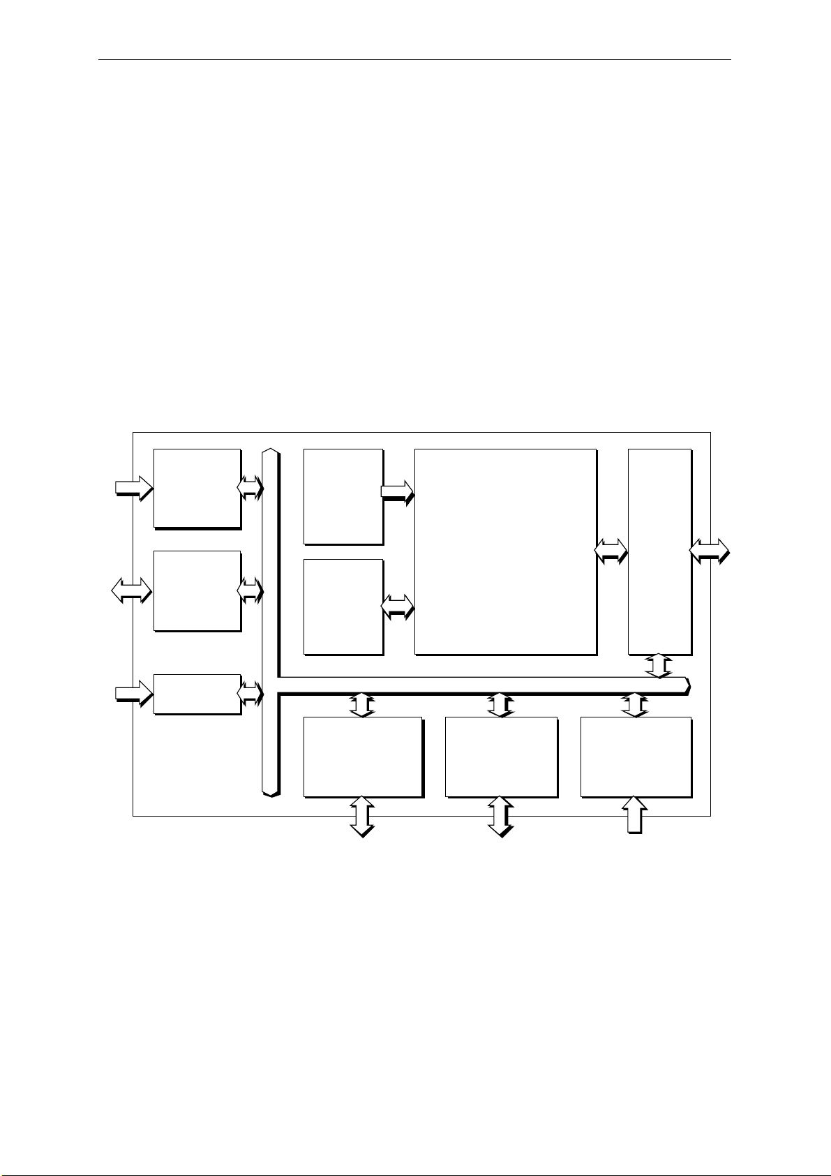
1.3 Block Diagram
A/D
10-bit
4 inputs
SIF
UART x 1
multipurpose x 1
synchronous system x 2
Clock and
system controller
ROM
128 KB
(flash memory
256 KB)
32-bit
CPU core
Data
RAM
8 KB
I/O ports
72 pins
(all multipurpose)
Fig. 1-3-1 MN103001G Block Diagram
Timers
16-bit x 4
8-bit x 12
WDT x 1
Bus
controller
includes
DRAM
controller
Interrupt
controller
38 sources
* The MN1030F01K (flash version) is equipped with 256 KB of flash memory instead of 128 KB of ROM.
1-4
Page 31

1.4 Pin Description
1.4.1 Pin Assignments
The pin assignments are shown in Fig. 1-4-1 and Table 1-4-1.
P55/SBO3/TM5IO/TM13IO
P54/SBI3/TM4IO/TM12IO
P53/SBT3/TM3IO/TM11IO
P52/SBO2/TM2IO
P51/SBI2/TM1IO
P50/SBT2/TM0IO
P45/SBO1/DWE
VDD
P44/SBI1/DCAS1
P43/SBT1/DCAS0
VSS
P42/SBO0
P41/SBI0
P40/SBT0
62
63
64
65
66
67
68
69
70
71
72
73
74
75
P30/BG
P27/D15
P26/D14
VDD
P25/D13
P24/D12
P23/D11
P22/D10
P21/D9
VSS
VDD2(VPP)*
P20/D8
P17/D7
P16/D6
P15/D5
P14/D4
VDD
P13/D3
P12/D2
P11/RWSEL/D1
P10/AS/D0
P02/CAS/A22
VSS
P01/A21
P00/A20
76
77
78
79
80
81
82
83
84
85
86
87
88
89
90
91
92
93
94
95
96
97
98
99
100
TOP VIEW
100-Pin QFP
9
8
7
6
5
4
3
2
1
10
11
12
13
14
P62/IRQ2/TM10IOA
P61/IRQ1/TM7IO
P60/IRQ0/TM6IO
VSS
NMIRQ
57
58
59
60
61
19
18
17
16
15
General Specifications
P73/A23/CS3
P72/RAS2/CS2
P71/RAS1/CS1
VDD
P70/CS0
P63/IRQ3/ADTRG/TM10IOB
51
52
53
54
55
56
20
21
22
23
24
50
49
48
47
46
45
44
43
42
41
40
39
38
37
36
35
34
33
32
31
30
29
28
27
26
25
AVDD
VREFH
P80/AN0/IRQ4
P81/AN1/IRQ5
P82/AN2/IRQ6
P83/AN3/IRQ7
AVSS
EXMOD0/P90
EXMOD1/P91
VDD
P92/RE
P93/WE0
P94/WE1
P95/DK
P96/BR
VSS
SYSCLK/P97
VDD
OSCI
OSCO
RST
MMOD0
MMOD1
PVDD
PVSS
VDD
PC1/A17
PC2/A18
PC3/A19
VSS
PC0/A16
PB4/ADM12/A12
PB5/ADM13/A13
PB6/ADM14/A14
PB7/ADM15/A15
VDD
PB0/ADM8/A8
PB1/ADM9/A9
PB2/ADM10/A10
PB3/ADM11/A11
PA6/ADM6/A6
PA7/ADM7/A7
VSS
PA1/ADM1/A1
PA2/ADM2/A2
PA3/ADM3/A3
PA4/ADM4/A4
PA5/ADM5/A5
CKSEL
PA0/ADM0/A0
Fig. 1-4-1 Pin Assignments Diagram
* "VDD2" in the case of the MN103001G, "VPP" in the case of the MN1030F01K.
1-5
Page 32

General Specifications
Table 1-4-1 Pin Assignments
Pin
Pin Name
No.
1 PC3/A19 26 PVSS 51 P73/A23/CS3 76 P30/BG
2 PC2/A18 27 PVDD 52 P72/RAS2/CS2 77 P27/D15
3 VDD 28 MMOD1 53 P71/RAS1/CS1 78 P26/D14
4 PC1/A17 29 MMOD0 54 VDD 79 VDD
5 PC0/A16 30 RST 55 P70/CS0 80 P25/D13
6 PB7/ADM15/A15 31 OSCO 56 P63/IRQ3/ADTRG/TM10IOB 81 P24/D12
7 PB6/ADM14/A14 32 OSCI 57 P62/IRQ2/TM10IOA 82 P23/D11
8 PB5/ADM13/A13 33 VDD 58 P61/IRQ1/TM7IO 83 P22/D10
9 VSS 34 SYSCLK/P97 59 P60/IRQ0/TM6IO 84 P21/D9
10 PB4/ADM12/A12 35 VSS 60 VSS 85 VSS
11 PB3/ADM11/A11 36 P96/BR 61 NMIRQ 86 VDD2(VPP) *
12 PB2/ADM10/A10 37 P95/DK 62 P55/SBO3/TM5IO/TM13IO 87 P20/D8
13 PB1/ADM9/A9 38 P94/WE1 63 P54/SBI3/TM4IO/TM12IO 88 P17/D7
14 PB0/ADM8/A8 39 P93/WE0 64 P53/SBT3/TM3IO/TM11IO 89 P16/D6
15 VDD 40 P92/RE 65 P52/SBO2/TM2IO 90 P15/D5
16 PA7/ADM7/A7 41 VDD 66 P51/SBI2/TM1IO 91 P14/D4
17 PA6/ADM6/A6 42 EXMOD1/P91 67 P50/SBT2/TM0IO 92 VDD
18 PA5/ADM5/A5 43 EXMOD0/P90 68 P45/SBO1/DWE 93 P13/D3
19 PA4/ADM4/A4 44 AVSS 69 VDD 94 P12/D2
20 PA3/ADM3/A3 45 P83/AN3/IRQ7 70 P44/SBI1/DCAS1 95 P11/RWSEL/D1
21 VSS 46 P82/AN2/IRQ6 71 P43/SBT1/DCAS0 96 P10/AS/D0
22 PA2/ADM2/A2 47 P81/AN1/IRQ5 72 VSS 97 P02/CAS/A22
23 PA1/ADM1/A1 48 P80/AN0/IRQ4 73 P42/SBO0 98 VSS
24 PA0/ADM0/A0 49 VREFH 74 P41/SBI0 99 P01/A21
25 CKSEL 50 AVDD 75 P40/SBT0 100 P00/A20
Pin
No.
Pin Name
Pin
No.
Pin Name
Pin
No.
Pin Name
• Pins for which two or more names are shown are multipurpose pins.
* "VDD2" in the case of the MN103001G, "VPP" in the case of the MN1030F01K.
1-6
Page 33

1.4.2 Pin Functions
Table 1-4-2 shows the function of each pin of this microcontroller.
Table 1-4-2 Pin Function Table (1/2)
General Specifications
Category Pin name
Power supply VDD 8 Digital system power supply (+3.3 V)
VSS 7 Digital system GND
VDD2(VPP) 1 “VDD2” in the case of the MN103001G, “VPP” in the
Clock OSCI I 1 Oscillator input
OSCO O 1 Oscillator output
SYSCLK O 1 System clock output (multipurpose)
CKSEL I 1 Switch for using/not using PLL
PVDD 1 PLL power supply (+3.3 V)
PVSS 1 PLL GND
Address bus A23 to 0 O 24 Address lines 23 to 0 (multipurpose, A23 also serves as
Data bus D15 to 0 I/O 16 Data lines 15 to 0 (multipurpose)
Address/ ADM15 to 0 I/O (16) Address/Data lines 15 to 0 (A15 to 0 multipurpose)
Data bus
Bus control MMOD1 to 0 I 2 Mode setting signals
signals EXMOD1 to 0 I 2 Extension mode setting (multipurpose)
RE O 1 Memory read signal (multipurpose)
CS3 to 0 O 4 Chip select signals (multipurpose)
WE1 to 0 O 2 Memory write signals (multipurpose)
DK I 1 Data acknowledge signal (multipurpose)
BG O 1 Bus authority release signal (multipurpose)
BR I 1 Bus authority request signal (multipurpose)
CAS O (1) DRAM CAS signals (for 2WE) (multipurpose of A22)
RAS2 to 1 O (2) DRAM RAS signal (multipurpose of CS2 to 1)
AS O (1) Address strobe signal (Also serves as D0.)
RWSEL O (1) Read/write select (Also serves as D1.)
DCAS1 to 0 O (2) DRAM CAS signal (for 2 CAS)
DWE O (1) DRAM write signal (for 2 CAS)
Input/ Number
Output of pins
Pin Function
case of the MN1030F01K. Connect to 5 V or 3.3 V.
Always input 5 V to VPP when writing.
(use input of 3.3 V to 0 V amplitude only.)
(Open when using an external clock input)
CS3.)
1-7
Page 34

General Specifications
Table 1-4-2 Pin Function Table (2/2)
Category Pin name
Reset RST I 1 Reset input
Interrupts NMIRQ I 1 External non-maskable interrupt input
IRQ7 to 0 I 8 External interrupt 7 to 0 inputs (multipurpose)
Serial interface SBI3 to 0 I 4 Serial 3 to 0 data inputs (multipurpose)
SBO3 to 0 I/O 4 Serial 3 to 0 data inputs/outputs (multipurpose)
SBT3 to 0 I/O 4
8-bit timer TM7IO to I/O (8) PWM output/Toggle output/shared by event count
TM0IO input
16-bit timer TM10IOA I/O (1) PWM output/capture input (multipurpose of IRQ2 )
TM10IOB I/O (1) PWM output/capture input (multipurpose of IRQ3)
TM13IO to I/O (3) Dual use for event count/toggle output
TM11IO
A/D converter VREFH I 1 A/D converter reference voltage input
ADTRG I (1) A/D converter trigger conversion input (multipurpose
AN3 to 0 I (4) A/D converter analog signal inputs (multipurpose of
AVDD 1 Analog system power supply (+3.3 V)
AVSS 1 Analog system GND
I/O ports P02 to P00 O (3) Port 0; output port (multipurpose)
P17 to P10 I/O (8) Port 1; input/output port (multipurpose)
P27 to P20 I/O (8) Port 2; input/output port (multipurpose)
P30 I/O (1) Port 3; input/output port (multipurpose)
P45 to P40 I/O (6) Port 4; input/output port (multipurpose)
P55 to P50 I/O (6) Port 5; input/output port (multipurpose)
P63 to P60 I/O (4) Port 6; input/output port (multipurpose)
P73 to P70 O (4) Port 7; output port (multipurpose)
P83 to P80 I (4) Port 8; input port (multipurpose)
P96, P95, P91, P90
P97, P94 to P92
PA7 to PA0 I/O (8) Port A; input/output port (multipurpose)
PB7 to PB0 I/O (8) Port B; input/output port (multipurpose)
PC3 to PC0 O (4) Port C; output port (multipurpose)
Input/ Number
Output of pins
(SBO3 is output only.)
Serial 3 to 0 transfer clock inputs/outputs (multipurpose)
(SBT3 is input only.)
(Use input of AVDD to 0 V only.)
of IRQ3)
IRQ7 to 4) (Use input of VREFH to 0 V only.)
I/O (4) Port 96, 95, 91, 90; input/output port (multipurpose)
O (4) Port 97, 94, 93, 92; output port (multipurpose)
Pin Function
Notes:
1. A number that is not enclosed in parentheses in the “Number of pins” column indicates the main pins, while a
number enclosed in parentheses indicates multipurpose pins.
2. After the reset condition is released, maintain the NMIRQ pin at the high level until the initialization routine
(which sets the stack pointer SP) is completed. If the NMIRQ pin is not used, connect it to VDD via a resistor.
1-8
Page 35

2. CPU
2
Page 36

CPU
2.1 Basic Specifications of CPU
• Structure Load/store architecture
Data/Address/SP Registers x 9
(Data registers: 32-bit x 4, Address registers: 32-bit x 4, SP: 32-bit x 1)
Other Registers
(PC: 32-bit x 1, PSW: 16-bit x 1, Multiply/divide register: 32-bit x 1,
Branch target registers: 32-bit x 2)
• Instructions Number of instructions : 46
Number of addressing modes : 6
Basic instruction length : 1 byte
Code assignment : 1 byte to 2 bytes (basic part)
• Basic performance Maximum internal operating
frequency : 60 MHz*1 (external oscillation: 15 MHz)
40 MHz*2 (external oscillation: 10 MHz)
Minimum instruction execution
cycle : 1 cycle (16.7 ns*1/25 ns*2)
Register-register operations : 1 cycle
Load/store : 1 cycle
Conditional branch : 1 cycle to 3 cycles
+ 0 byte to 6 bytes (extension)
• Pipeline 5-stage (Instruction fetch, decode, execute, memory access, write-back)
• Address space 4 GB
Unified space for instructions and data
(Instructions can not be read from internal data RAM.)
*1 in the case of the MN103001G.
*2 in the case of the MN1030F01K.
2-2
Page 37

2.2 Block Diagram
The block diagram for this microcontroller, focusing on the CPU, is shown below.
Address register Data register
CPU
User
extension
function unit
A0
A1
A2
A3
AU LU
Extension interface
D0
D1
D2
D3
Operand address
SP
MDR
PSW
Barrel
shifter
Operand data Instruction
Internal
data RAM
External interface
Program
counter
block
Bus contol block
AU
Instruction address
instruction ROM/
Instruction
execution
control block
Instruction
decoder
Instruction
queue
Internal
Internal flash
memory
Internal
peripheral
function
Interrupt
control
block
Fig. 2-2-1 CPU Core Block Diagram
2-3
Page 38

CPU
2.3 Programming Model
2.3.1 CPU Registers
• The register set is divided into data registers that are used for arithmetic operations, etc., address registers that
are used for pointers, and a stack pointer. This arrangement contributes greatly to the improved performance of
the internal architecture, through reduction of instruction code size, improved parallelism in pipeline processing,
etc.
• This register enables programming in C and other high-level languages.
Data Register
Address Register
Stack Pointer
Program Counter
Multiply/Divide Register
Processor Status Word
Loop Instruction Register
31
31
31
31
31
31
D0
D1
D2
D3
A0
A1
A2
A3
SP
PC
MDR
15
LIR
0
0
0
0
0
0
PSW
0
Loop Address Register
31
LAR
0
Fig. 2-3-1 CPU Registers
• The loop instruction register (LIR) and the loop address register (LAR) are used to provide high-speed execution
of branch instructions. High-speed loop control is performed by loading the branch target instruction and following
fetch address with the SETLB instruction and forming the loop using the Lcc instruction.
2-4
Page 39

■ Data Register (32-bit x 4)
This register can be used generally for all operations. Operations are performed with a 32-bit length and the data
size is converted when sending data to and from the memory or by executing the EXTB or EXTH instructions.
When loading data, 8-bit data is zero-extended to 32 bits and sent to the register. When storing data, the lower 8
bits of the register are sent to the memory. When handling the loaded 8-bit data as a signed integer, the data is
sign-extended from 8 bits to 32 bits with the EXTB instruction. When loading data, 16-bit data is zero-extended
to 32 bits and sent to the register. When storing data, the lower 16 bits of the register are sent to the memory.
When handling the loaded 16-bit data as a signed integer, the data is sign-extended from 16 bits to 32 bits with
the EXTH instruction.
■ Address Register (32-bit x 4)
This register is used as an address pointer, and only instructions (addition, subtraction and comparison) for
address calculation are supported.
The address register data is used for pointers, and data is normally sent to and from the memory with a 32-bit
length.
■ Stack Pointer (32-bit x 1)
This pointer designates the first address of the stack region.
CPU
■ Program Counter (32-bit x 1)
This counter designates the address of the command being executed.
■ Multiply/Divide Register (32-bit x 1)
This register is provided for multiply and divide instructions. It holds the upper 32 bits of 64-bit multiplication
results for multiply instructions and the remainder (32 bits) for divide instructions. Also, the upper 32 bits of the
dividend are loaded to this register before executing divide instructions.
■ Processor Status Word (16-bit x 1)
This register indicates the CPU status, and contains the operation result flags and interrupt mask level, etc.
15
0
S1 S0 IE IM2 IM1
0
Fig. 2-3-2 Processor Status Word
IM0
0000
VCN
0
Z
2-5
Page 40

CPU
Z: Zero Flag
This flag is set when an operation result is all zeroes, and is cleared by any other result. This flag is
also cleared by a reset.
N: Negative Flag
This flag is set if the MSB of an operation result is "1", and is cleared if the MSB is "0". This flag
is also cleared by a reset.
C: Carry Flag
This flag is set when a carry or borrow to or from the MSB is generated in the course of executing an
operation, and is cleared if no carry or borrow is generated. This flag is also cleared by a reset.
V: Overflow Flag
This flag is set when an overflow occurs in a signed value in the course of executing an operation,
and is cleared if no overflow is generated. This flag is also cleared by a reset.
IM2 to IM0: Interrupt Mask
These bits indicate the CPU interrupt mask level. The three bits define the mask level from level 0
(000) to level 7 (111), with level 0 being the highest mask level. The CPU accepts only those
interrupt requests of a level higher than the mask level indicated here.
When an interrupt is accepted, the IM bits are set to the priority level of that interrupt. Until the
processing of the accepted interrupt is completed, the CPU does not accept interrupts with the same
interrupt level or lower.
The interrupt mask level is set to level 0 (000) by a reset.
IE: Interrupt Enable
Setting this bit to “1” allows interrupts to be accepted.
Once the CPU accepts an interrupt request, the IE bit is cleared to "0" and further acceptance of
interrupts is prohibited. Accordingly, the IE bit must be reset when processing nested interrupts.
This bit is cleared when the system is reset.
S1 to S0: Software Bits
These are the software control bits for the operating system. These bits cannot be used by general
user programs. These bits are cleared by a reset.
For details on changes of these flags, refer to the "Instruction Manual".
■ Loop Instruction Register (32-bit x 1)
This register is provided for the branch instruction (Lcc), and is used to load branch target instructions with the
SETLB instruction. This register works together with the Lcc instruction to enable high-speed loop control.
■ Loop Address Register (32-bit x 1)
This register is provided for the branch instruction (Lcc), and is used to load following fetch addresses with the
SETLB instruction.
2-6
Page 41

CPU
2.3.2 Control Registers
This microcontroller uses the memory-mapped-I/O method and allocates the peripheral circuit registers to the
internal I/O space between addresses x'20000000 and x'3FFFFFFF.
The registers listed below are described in this section. For details on other control registers, refer to the respective
sections that explain the various internal peripheral functions.
Table 2-3-1 List of Control Registers
Address Name Symbol Number of bits Initial value Access size
x'20000000 Interrupt vector register 0 IVAR0 16 x'XXXX 16
x'20000004 Interrupt vector register 1 IVAR1 16 x'XXXX 16
x'20000008 Interrupt vector register 2 IVAR2 16 x'XXXX 16
x'2000000C Interrupt vector register 3 IVAR3 16 x'XXXX 16
x'20000010 Interrupt vector register 4 IVAR4 16 x'XXXX 16
x'20000014 Interrupt vector register 5 IVAR5 16 x'XXXX 16
x'20000018 Interrupt vector register 6 IVAR6 16 x'XXXX 16
x'20000020
x'20000040 CPU mode register CPUM 16 x'0000 16
Core's internal memory control register
MEMCTRC 16 x'0007 16
2-7
Page 42

CPU
Interrupt Vector Register (IVARn)
(n = 0, 1, 2, 3, 4, 5, 6)
The interrupt vector register (IVAR0 to IVAR6) contains the lower 16 bits of the start address of the interrupt
handler for interrupts of the level accepted by the CPU. IVAR0 corresponds to level 0 interrupts; in similar fashion,
IVAR1 to IVAR6 correspond to levels 1 to 6, respectively. IVAR0 to IVAR6 are allocated to the internal I/O space
between addresses x'20000000 to x'20000018, respectively.
Bit No. 15 14 13 12 11 10 9 8 7 6 5 4 3 2 1 0
Bit name
Reset XXXXXXXXXXXXXXXX
Access R/W R/W R/W R/W R/W R/W R/W R/W R/W R/W R/W R/W R/W R/W R/W R/W
IVAR IVAR IVAR IVAR IVAR IVAR IVAR IVAR IVAR IVAR IVAR IVAR IVAR IVAR IVAR IVAR
n15 n14 n13 n12 n11 n10 n9 n8 n7 n6 n5 n4 n3 n2 n1 n0
Bit No. Bit name Description
15 to 0 IVARn15 to 0 Lower 16 bits of the start address of the level interrupt handler
The IVARn register should be accessed by halfwords (16 bits). Byte and word access is not supported.
Note that the upper 16 bits of the start address of the level interrupt handler are fixed to x'4000.
Core's Internal Memory Control Register (MEMCTRC)
The core's internal memory control register (MEMCTRC) sets the number of waits for the memory mounted inside
this microcontroller. This register is allocated to the internal I/O space at address x'20000020.
Bit No. 15 14 13 12 11 10 9 8 7 6 5 4 3 2 1 0
Bit name ————— ———— ———
Reset 00000 0000 0000111
Access RRRRR RRRR RRRRRRR
LD EXT DROM ROM
USE WAIT W WAIT
Writing these bits is prohibited, since operation is guaranteed only with the settings that are in place after a reset.
2-8
Page 43

CPU
CPU Mode Register (CPUM)
The CPU mode register (CPUM) sets the clock operating mode for the CPU and peripheral blocks. This register is
allocated to the internal I/O space at address x'20000040.
Bit No. 15 14 13 12 11 10 9 8 7 6 5 4 3 2 1 0
Bit name ————————— —OSCID STOP HALT SLEEP OSC1 OSC0
Reset 000000000 0000 00 0
Access R R R R R R R R R R R R/W R/W R/W R/W R/W
Bit No. Bit name Description
0 OSC0 Always returns "0" when read. Always write "0".
1 OSC1 Always returns "0" when read. Always write "0".
2 SLEEP CPU operating mode control flag (SLEEP transfer request)
3 HALT CPU operating mode control flag (HALT transfer request)
4 STOP CPU operating mode control flag (STOP transfer request)
5 OSCID Always returns "0" when read. Always write "0".
15 to 6 — reserved
The various operating modes can be set by setting the bits as shown in the table below.
Oscillation control and operating mode control
Operating mode STOP HALT SLEEP OSC1 OSC0
Clock CPU operation Peripheral function
oscillation clock operation clock
NORMAL 0 0 0 0 0 Oscillating Running Running
HALT 0 1 0 0 0 Oscillating Stopped Stopped
SLEEP 0 0 1 0 0 Oscillating Stopped Running
STOP 1 0 0 0 0 Stopped Stopped Stopped
The CPUM register should be accessed by halfwords (16 bits). Byte and word access is not supported.
If the CPUM register is accessed to make a transition to an operating mode of SLEEP/HALT/STOP during execution
of a program in external memory, a branch instruction should not be located within the three instructions immediately
following the CPUM register access instruction.
2-9
Page 44

CPU
2.4 Instructions
2.4.1 Addressing Modes
The 32-bit microcontroller is equipped with the following 6 addressing modes which are frequently used with
compilers.
All 6 addressing modes of register direct, immediate value, register indirect, register indirect with displacement,
absolute and register indirect with index can be used with data transfer group instructions.
The 2 addressing modes of register direct and immediate addressing can be used with register operation instructions.
Register indirect with index addressing is an addressing mode used to efficiently access arrays and other data.
Table 2-4-1 Addressing Mode Types
Addressing mode
Register direct
Immediate value
Register indirect
Register indirect
with displacement
Dm / Dn
Am / An
imm8 / regs
imm16
imm32
imm40
imm48
(Am) / (An)
(d8, Am)/(d8, An)
: d8 is sign-extended
(d16, Am)/(d16, An)
: d16 is sign-extended
(d32, Am)/(d32, An)
(Branch instructions only)
(d8, PC)
: d8 is sign-extended
(d16, PC)
: d16 is sign-extended
(d32, PC)
Address calculation Effective address
Am/An
Am/An
+
031
031
715 031
(32-bit address)
(32-bit address)
d32/d16/d8
031
PC
(32-bit address)
+
715 031
d32/d16/d8
031
031
031
(d8, SP)
: d8 is zero-extended
(d16, SP)
: d16 is zero-extended
(d32, SP)
(abs16)
Absolute
: abs16 is zero-extended
(abs32)
Register indirect with index
(Di, Am)/(Di, An)
SP
+
d32/d16/d8
15
abs32/abs16
Am/An
+
031
(32-bit address)
715 031
031
(32-bit address)
031
(32-bit address)
031
031
031
031
Di
When accessing data using the register indirect with displacement and register indirect with index modes, the base
address (the contents of Am, An and SP) and the effective address must be located within the same address space.
For details on memory spaces, refer to section 4.1, "Memory Mode Types and Selection."
2-10
Page 45

CPU
2.4.2 Data Types
Data types can be processed in the four types of bit, byte, halfword and word data. Byte data, halfword data and
word data can be handled as signed and unsigned data. The sign bit is MSB.
The data in the memory must be aligned data. In other words, the two bits on the LSB side of addresses containing
word data must be "00" (addresses which are a multiple of 4), and the LSB of addresses containing halfword data
must be "0" (addresses which are a multiple of 2).
Byte and bit placement conforms with the Little Endian format. Therefore, the address of the byte data on the MSB
side of halfword data is the LSB side byte data address + 1,and the address of the byte data on the MSB side of word
data is the LSB side byte data address + 3. The bit number for bit data starts at 0 on the LSB and increases towards
the MSB.
Table 2-4-2 Data Types
(1) Bit data
(2) Byte data
Unsigned 8-bit
Signed 8-bit (sign bit: MSB)
(3) Halfword data
Unsigned 16-bit
Signed 16-bit (sign bit: MSB)
(4) Word data
Unsigned 32-bit
Signed 32-bit (sign bit: MSB)
MSB LSB
Bit No. 31 24 23 16 15 8 7 0
Address in the memory
Word data
Halfword data
Byte data
Upper halfword Lower halfword
Most significant byte Least significant byte
Most significant byte Least significant byte
4n4n+14n+24n+3
Fig. 2-4-1 Little Endian Format
2-11
Page 46

CPU
2.4.3 Instruction Set
The instruction set has a simple organization, and features the generation of compact and optimized code through a
C compiler.
The instruction code size is reduced by making the basic instruction word length one byte. As a result, increases in
the code size of the assembler program can be kept to a minimum even though the instruction set is simple, with
data transfers to and from memory limited to load and store operations.
Table 2-4-3 Instruction Types (All 46 types and extension instructions)
• Transfer instructions
MOV Transfer of word data between registers
Transfer of word data between registers and the memory
Transfer of immediate values to registers
MOVBU Transfer of byte data between registers and the memory
(zero-extension)
MOVHU Transfer of halfword data between registers and the memory
(zero-extension)
EXT 64-bit sign-extension of word data
EXTB 32-bit sign-extension of byte data
EXTBU 32-bit zero-extension of byte data
EXTH 32-bit sign-extension of halfword data
EXTHU 32-bit zero-extension of halfword data
MOVM Transfer between multiple registers and the memory
CLR Data clear
• Arithmetic instructions
ADD Addition
ADDC Addition with carry
SUB Subtraction
SUBC Subtraction with borrow
MUL Signed multiplication
MULU Unsigned multiplication
DIV Signed division
DIVU Unsigned division
INC Increment by 1
INC4 Increment by 4
• Compare instructions
CMP Compare
• Logical instructions
AND And
OR Inclusive Or
XOR Exclusive Or
NOT Not (complement of 1)
2-12
Page 47

CPU
• Bit instructions
BTST Bit Test
BSET Test and set (processing unit: byte)
BCLR Test and clear (processing unit: byte)
• Shift instructions
ASR Shift Right Arithmetic
LSR Shift Right Logical
ASL Shift Left Arithmetic
ASL2 Shift Left 2-bit Arithmetic
ROR Rotate 1 bit to the right
ROL Rotate 1 bit to the left
• Branch instructions
Bcc Branch on condition codes (PC relative)
Lcc Loop on condition codes (PC relative)
SETLB Set loop buffer
JMP Unconditional branch (PC relative, register indirect)
CALL Subroutine call (Advanced function)
CALLS Subroutine call
RET Return from subroutine (Advanced function)
RETF Return from subroutine (Advanced function, high-speed)
RETS Return from subroutine
RTI Return from interrupt program
TRAP Subroutine call to specified address
NOP No operation
• Extension instructions
UDF User extension instruction (sign-extension)
UDFU User extension instruction (zero-extension)
Note:
Interrupts are prohibited and the bus is locked (occupied by the CPU) when executing BSET or BCLR, however, if
a BSET or BCLR instruction is executed during program execution in external memory, a bus authority release due
to an external bus request may be interposed between the data read and data write by the BSET or BCLR instruction.
If the atomic bus cycles (i.e. bus lock) of the BSET or BCLR instruction need to be guaranteed in a system that uses
multiple processors, either of the following measures should be taken.
1. A program in which a BSET or BCLR instruction is executed should be placed in internal memory.
2.
Designate the bus authority request pin (BR) as a general-purpose input port, and the bus authority release pin
_____
_____
(BG) as a general-purpose output port, for instance, so that bus requests cannot be accepted during execution of
a BSET or BCLR instruction.
2-13
Page 48

CPU
2.5 Interrupts
2.5.1 Overview of Interrupts
The most important key to real-time control is the ability to shift quickly to interrupt handler processing.
If an interrupt is generated during the execution of an instruction that requires multiple cycles for execution
(multiplication or division instructions, for example), interrupt response is improved by aborting the execution of
the instruction and immediately accepting the interrupt. After control returns from the interrupt processing program,
the aborted instruction is re-executed.
In addition, by minimizing the resources saved to memory to just the 6 bytes of the PC and the PSW when an
interrupt is generated, the speed of interrupt processing is improved, as is the flexibility of software control.
Furthermore, fast response and optimal program allocation are possible by placing interrupt processing programs at
different addresses for each interrupt level.
This microcontroller has the interrupts shown below. When any of these interrupts occurs, control is shifted to the
appropriate processing program in accordance with the cause.
Reset interrupt
Non-maskable interrupt Priority ranking
Level interrupt n (n = 0 to 6)
➤
Fig. 2-5-1 shows an overview of the interrupt system. This microcontroller is equipped with 19 interrupt group
control blocks outside the CPU, and controls the interrupts of each group separately. Each interrupt group control
block can accept up to 4 interrupt requests. This allows the controller to support to 38 interrupt factors, providing it
with high expandability and enabling flexible ASIC support.
Except for the reset interrupt, all interrupts from the timer and other peripheral circuits and external pin interrupts
are registered in the interrupt group control blocks. Then, the interrupt requests which pass the interrupt priority
level (level 0 to 6) set in the interrupt group control blocks are output to the CPU. Groups 0 is assigned to nonmaskable interrupts only.
CPU
71
Group 0
Interrupt group control
Group 2
Interrupt group control
4
Interrupt
Interrupt
4
Non-maskable interrupts
3 factors are allocated to this group: external pin non-maskable
interrupt, watchdog timer overflow interrupt and system error
interrupt. The remaining factor is reserved.
2-14
Group 19
Interrupt group control
Interrupt controller (INTC)
Fig. 2-5-1 Overview of the Interrupt System
External interrupts
8 external pin interrupts as well as timer, serial
and other peripheral interrupts are assigned.
4
Interrupt
Page 49

2.5.2 Registers [Flags in the PSW] (CPU)
Interrupt-related flags in the processor status word (PSW) include interrupt enable and interrupt mask level.
IE (Interrupt Enable) R/W
• This flag allows all interrupts to be accepted except for non-maskable interrupts and reset interrupts.
Interrupts are allowed when IE = 1. IE = 0 when the system is reset.
• When an interrupt is accepted, IE is cleared (interrupt prohibited). Set IE when accepting nested
interrupts within the interrupt handler.
IM2 to IM0 (Interrupt Mask Level) R/W
• This holds the current interrupt mask level. When IE = 1, CPU accepts interrupts with levels higher
than IM2 to IM0. Level 0 (000) when the system is reset.
• The following table shows the relationship between mask levels and acceptable interrupt levels.
Table 2-5-1 Relationship between Mask Levels and Interrupt Levels that Can Be Accepted
CPU
Interrupt mask level
Acceptable interrupt level
IM2 IM1 IM0
000
Interrupt prohibited (only non-maskable interrupts accepted)
0010
0100-1
0110-2
1000-3
1010-4
1100-5
1110-6
[Interrupt Control Registers (GnICR)] R/W halfword/byte access
Interrupt control registers (GnICR: n = 0, 2 to 19) combine interrupt priority level, interrupt enable, interrupt
request and interrupt detect fields into a single register in order to control CPU external peripheral interrupts. There
are 19 interrupt control registers, one for each group, and they are located in the internal I/O space from x'34000100
to x'3400014C. Register G0ICR is dedicated for non-maskable interrupts, and G0ICR is called NMICR (from the
least significant bit: external pin non-maskable interrupt, watchdog timer overflow interrupt, system error interrupt).
Fig. 2-5-2 shows the interrupt control register (GnICR) configuration, and each field is described in detail as
follows.
G0ICR (NMICR)
GnICR (n = 2 to 19)
15
1413121110987654321
0ID
000000 00000
15
1413121110987654321
LV IE IR
0ID
0
0
Fig. 2-5-2 Interrupt Control Register (GnICR)
2-15
Page 50

CPU
LV2 to LV0 (Interrupt Priority Level) R/W
• This 3-bit field sets the interrupt priority level. When the interrupt priority level set in LV2 to LV0
is higher than the interrupt mask level set in IM2 to IM0 in the PSW (i.e., the value set in LV2 to
LV0 is smaller than the value set in IM2 to IM0), interrupts in the corresponding interrupt group
are enabled. All interrupts (max. 4) in the same interrupt group have the interrupt priority level
specified by LV2 to LV0.
• When interrupt requests are asserted simultaneously from multiple interrupt groups, the group with
the highest interrupt priority level is accepted. Also, when multiple interrupt groups are set to the
same interrupt priority level, the interrupt from the group with the highest priority ranking (the
interrupt group with the smallest group number) is accepted.
• All bits are cleared to "0" when the system is reset.
IE3 to IE0 (Interrupt Enable) R/W
• This field has up to 4 bits which specify interrupt approval. The IE3 to IE0 bits correspond to each
interrupt factor (max. 4) in the interrupt group. Interrupts are enabled when the corresponding IE3
to IE0 bit is "1".
• Interrupt occurs when IR3 to IR0 and IE3 to IE0 are set.
• All bits are cleared to "0" when the system is reset.
IR3 to IR0 (Interrupt Request) R/W
• This field has up to 4 bits which register interrupt requests. The IR3 to IR0 bits correspond to each
interrupt. After the interrupts are accepted, IR3 to IR0 should be cleared by the software during the
interrupt handler.
• All bits are cleared to "0" when the system is reset.
• Conditions for setting and clearing IR3 to IR0 are listed below.
ID3 to ID0 (Interrupt Detect) R/W
• This field has up to 4 bits which contain the logical product of IE3 to IE0 and IR3 to IR0. When an
interrupt allowed by IE3 to IE0 occurs, the bit corresponding to that interrupt goes to "1". This field
is used to specify interrupts within groups during interrupt processing.
• Interrupt requests are canceled by writing the specified values in IR3 to IR0 and ID3 to ID0 and
clearing the interrupt request field.
ID change (G0ICR) IR change (GnICR: n = 2 to 19)
Write
ID
0 Unchanged
10
ID after write
Write
IR ID
0 0 Unchanged
01 0
1 0 Unchanged
11 1
IR after write
2-16
Page 51

CPU
[Interrupt Accept Group Register (IAGR)] R halfword/byte access
During a register read, the interrupt accept group register (IAGR) indicates the smallest group number of the groups
that are generating an interrupt of the interrupt levels accepted by the CPU, which are indicated by IM2 to IM0 of
the PSW. This register is allocated to address x'34000200 in the internal I/O space. The GN4 to GN0 field (5 bits)
corresponds to the interrupt group number. A branch destination of the interrupt program for each group can be
found, for example, by referencing the contents of the address obtained by adding the interrupt accept group register
value to the leading address of the interrupt vector table. The interrupt accept group register is a read only register,
and writing cannot be performed. When there are no interrupt factors of the applicable interrupt level, IAGR
becomes 0.
Accessing IAGR is meaningless during non-maskable interrupts.
IAGR
1413121110987654321
15
0
000000 0
0
GN
0
0
0
Fig. 2-5-3 Interrupt Accept Group Register
[Interrupt Vector Address Register (IVARn)] R/W halfword access
The interrupt vector register (IVAR0 to IVAR6) contains the lower 16 bits of the start address of the interrupt
handler for interrupts of the accepted level. This register is allocated between addresses x'20000000 to x'20000018
in the internal I/O space. The start address of interrupt levels 0 to 6 correspond to IVAR0 to IVAR6. When an
interrupt occurs, control is transferred to the address which is comprised of the upper 16 bits (x'4000) and the lower
16 bits (IVARn). This register is undefined when the system is reset.
IVARn
141312111098 7654321
15
0
Fig. 2-5-4 Interrupt Vector Address Register
2-17
Page 52

CPU
2.5.3 Interrupt Types
The three types of interrupts are listed below:
[Reset interrupt]
The reset interrupt is the interrupt with the highest priority level, and is generated by setting the RST pin to "L"
level. As a result of the reset interrupt, the registers, etc., are initialized. When the RST pin goes to "H" level, the
microcontroller waits until the oscillation of the internal clock stabilizes, and then begins executing program
instructions starting from address x'40000000.
[Non-maskable Interrupts]
Non-maskable interrupts are accepted regardless of the PSW interrupt enable (IE) and interrupt mask level IM2 to
IM0 values. These interrupts include external pin non-maskable interrupt, watchdog timer overflow interrupt and
system error interrupt.
When a non-maskable interrupt is accepted, control transfers to an interrupt processing program located at x'40000008
or beyond.
The interrupt handler accesses NMICR to analyze the interrupt factor, performs interrupt processing, cancels the
interrupt factor, and then returns to the normal program using the RTI instruction.
External pin non-maskable interrupt
External pin non-maskable interrupt is generated when the NMIRQ pin goes to "L" level. If an external pin
non-maskable interrupt is generated, the external non-maskable interrupt request flag (NMIF) in the nonmaskable interrupt control register (NMICR) is set to "1".
Watchdog timer overflow interrupt
Watchdog timer overflow interrupt occurs when the watchdog timer count operation control flag (WDCNE)
in the watchdog timer control register (WDCTR) is "1" and the watchdog timer overflows. If a watchdog
interrupt is generated, the watchdog timer overflow interrupt request flag (WDIF) in the non-maskable interrupt
control register (NMICR) is set to "1".
System error interrupt
System error interrupt occurs when an unaligned memory access or an unimplemented instruction is executed
or other fatal error occurs. If a system error interrupt is generated, the system error interrupt request flag
(SYSEF) in the non-maskable interrupt control register (NMICR) is set to "1".
Note: Do not change the interrupt enable (IE) in PSW during non-maskable interrupt processing.
2-18
Page 53

CPU
[Level interrupts]
Level interrupts are interrupts for which the interrupt level can be controlled through the interrupt enable (IE) and
interrupt mask (IM2 to IM0) bits in the PSW. Level interrupts are interrupts from the interrupt group controllers
external to the CPU (in other words, peripheral interrupts). There are 18 groups, or 35 interrupt factors.
Each interrupt group controller includes an interrupt control register (GnICR); the interrupt priority level can be set
independently for each interrupt group. It is also possible to set the same interrupt priority level for different
interrupt groups. If interrupts of the same priority level are generated simultaneously, the interrupts are accepted in
the sequence set by the hardware (the lower the interrupt group number, the higher the priority).
When a level interrupt is accepted, the hardware causes the program to branch to an address with the upper 16 bits
being "x'4000" and the lower 16 bits indicated by the interrupt vector address register IVARn corresponding to the
interrupt level.
The interrupt handler accesses IAGR to analyze the interrupt group, accesses GnICR (n = 2 to 19) to analyze the
interrupt factor, performs interrupt processing, cancels the interrupt factor, and then returns to the normal program
using the RTI instruction.
2.5.4 Interrupt Definition
When this microcontroller accepts an interrupt, first the sequences automatically processed by the hardware are
executed. Then control transfers to interrupt handler by the software and the interrupt handler is started up.
The interrupt processing sequences are described below.
(Interrupt processing sequences executed by the hardware)
1. The PSW is saved to the stack (SP-8).
2. The PC (return address) is saved to the stack (SP-4).
3. The PSW is updated.
IE is cleared and the accepted interrupt level is set in IM2 to IM0. (IM2 to IM0 is undefined in case of nonmaskable interrupts.)
4. The stack pointer is updated. (SP-8 → SP)
5. Control is transferred to the address corresponding to the accepted interrupt factor or the address comprised of
the interrupt vector address register (IVARn).
When an interrupt other than a reset interrupt is accepted, control is transferred to the address corresponding to the
interrupt factor or the address comprised of the interrupt vector address register. The processing listed below is then
performed at the branch destination in order to judge the interrupt factor in further detail.
See "2.5.3 Interrupt Types" for processing reset interrupts.
(Note) In General, Branch instructions (JMP instruction, etc.) are placed at the branch destination for reset interrupts,
then it branches to the initialization program.
2-19
Page 54

CPU
(Example of pre-processing by the interrupt handler)
1. The registers are saved.
The saved registers are those used by the interrupt handler.
2. The interrupt group analysis is executed.
2.1 The interrupt acknowledge sequence is executed.
Interrupt acknowledge consists of reading out the interrupt accept group register (IAGR) to obtain the group
number of the interrupt group with the highest priority among the specified interrupt levels.
2.2 The leading address of the interrupt handler for each level is generated.
2.3 Control is transferred to the interrupt handler for each level.
3. When there are multiple factors within the same group, the interrupt control register (GnICR) is read out to
designate the factor.
* In case of non-maskable interrupts, the factor is specified by accessing the NMICR directly without accessing
the IAGR.
4. Control is transferred to the interrupt handler for each factor.
Note that because this microcontroller uses a store buffer when writing data via the bus controller, it is necessary,
when releasing the interrupt factor, to read the appropriate register immediately after clearing the interrupt
factor in order to wait for the factor in the GnICR to be cleared completely.
(Example of post-processing by the interrupt handler)
5. The registers are restored.
The restored registers are those saved by the pre-processing.
6. The RTI instruction is executed and control returns to the program before the interrupt.
Fig. 2-5-5 shows the interrupt sequence flow. (when not accepting nested interrupts)
The numbers in the figure correspond to the numbers of processing performed by the interrupt handler in the
previous section.
Interrupt
max. 11 Cycles
Program Handler (pre-processing)
Interrupt processing by hardware
3 Cycles
Processing for each level
1
2
Processing for each group
3
4
Interrupt
handler
Processing for
each factor
Interrupt processing
and interrupt request
cancel
2-20
RTI
5
6
Fig. 2-5-5 Interrupt Sequence Flow
Handler (post-processing)
Page 55

CPU
An even higher interrupt response speed can be realized by assigning only one factor or only a few factors to a
single interrupt level.
Fig. 2-5-6 shows the interrupt sequence flow when assigning one factor to each interrupt level.
Interrupt
max. 11 Cycles
Program
3 Cycles
Interrupt processing by hardware
RTI
Processing for each factor
1
Handler (pre-processing)
Interrupt
handler
5
Handler (post-processing)
6
Fig. 2-5-6 Interrupt Sequence Flow
[Nested Interrupts]
When a level interrupt occurs, nested interrupts can be prohibited by clearing IE of the PSW. However, nested
interrupts can be achieved even while processing level interrupts by setting IE to "1" during processing. However,
in order for nested interrupts to occur, the interrupts must have a higher priority than interrupt mask level IM2 to
IM0 of the PSW at that time. (The GnICR interrupt priority level LV2 to LV0 is smaller than the PSW interrupt
mask level IM2 to IM0.)
When non-maskable interrupts occur, nesting of level interrupts and non-maskable interrupts is prohibited until the
interrupt handler is finished by execution of the RTI instruction.
[Interrupt Acceptance Timing]
If an interrupt request occurs part-way through the execution of an instruction, even instructions which require
multiple execution cycles such as multiply/divide and other instructions are aborted if possible and the interrupt is
accepted. The aborted instruction is executed again after returning from interrupt processing. Aborting these
instructions sets the interrupt acceptance prohibited interval to 11 cycles or less. (The maximum interrupt prohibited
interval of 11 cycles occurs when saving or restoring all registers with the MOVM, CALL or RET instructions.
This occurs only for special cases such as task context switching.)
2-21
Page 56

CPU
[Stack Frame]
When an interrupt is accepted, a stack frame is allocated and the total 6 bytes of information in the PC and PSW are
saved in order to return from the interrupt. However, since the transfer of data across the 32-bit boundary is prohibited,
the SP value must constantly be set to a multiple of 4. Accordingly, a stack frame is allocated as shown in
Fig. 2-5-7 so that the SP value is constantly set to a multiple of 4. Ultimately, an 8-byte area with a total of 6 bytes
of information is saved.
+3 4n+2 +1
Smaller addresses
(Rsv.)
PC (Return address)
PSW
SP (After the interrupt)
SP (Before the interrupt)
Fig. 2-5-7 Stack Frame Configuration
2-22
Page 57

3. Extension Instruction Specifications
3
Page 58

Extension Instruction Specifications
3.1 Operation Extension Function
The MN1030 series 32-bit microcontrollers are provided with 32 extension instructions which can be defined by
users. This allows the desired processing to be performed at high speed for each model expansion by assigning
multiply, multiply-accumulate, saturation and other application-oriented operations to extension instructions and
connecting extension function unit via the extension operation interface of the CPU core.
Extension instructions include instructions UDF00 to UDF15 which transfer register or immediate values to the
extension function unit and load the operation results to the data register, and instructions UDF20 to UDF35 which
only transfer register to the extension function unit. Processing which performs user-defined operations is assigned
to instructions UDF00 to UDF15, and processing which only transfers data to the extension function unit is assigned
to instructions UDF20 to UDF35. Extension operations which require three or more inputs can be realized by
transferring the input data to the extension function unit beforehand using instructions UDF20 to UDF35 and then
performing the operation using instructions UDF00 to UDF15.
The block diagram showing extension function unit connected to the CPU for this series is as follows.
This microcontroller has a 32 x 16 multiplier, priority encoder, and saturation compensation unit on chip. The
extension functions that use the extension function unit are explained in section 3.2, "Extension Instructions."
Instruction
data
Program
counter
block
Instruction
address
Operation
extension block A
Instruction decoding
Register
Instruc-
tion
queue
Operand data
block
Barrel
shifter
CPU
instruction
decoder
AULU
Operand address
User
extension
instruction
decoder A
User extension
Operation extension interface
function unit
A
Fig. 3-1-1 Block Diagram of the Extension Function Unit
Operation
extension block B
User
extension
instruction
decoder B
User extension
function unit
B
......
......
......
3-2
Page 59

3.2 Extension Instructions
3.2.1 Explanation of Notations
The notations used to describe instruction manual are shown below.
OP: Opcode
Am, An: Address Register (m, n = 3 to 0)
Dm, Dn: Data Register (m, n = 3 to 0)
SP: Stack Pointer
imm: Immediate value (used as the general meaning)
imm8: 8-bit immediate value
imm16: 16-bit immediate value
imm32: 32-bit immediate value
d8: 8-bit displacement
d16: 16-bit displacement
d32: 32-bit displacement
abs16: 16-bit absolute
abs32: 32-bit absolute
MDR: Multiply/Divide Register (core built in)
MDRQ: High-speed multiplication register (inside Extension Function Unit)
LIR: Loop Instruction Register
LAR: Loop Address Register
PSW: Processor Status Word
PC: Program Counter
( ): Indirect addressing
See "2.4.1 Addressing Modes" for a detailed description.
regs: Multiple register operand
0x....: Hexadecimal notation (The numbers following 0x are expressed in hexadecimal notation.)
Extension Instruction Specifications
Notations used to express flag changes are listed below.
("Flag" is the general term used to refer to the lower 4 bits (V, C, N, Z) in the PSW.)
–: No flag change
+: Flag change
*: Undefined
0: Reset
1: Set
3-3
Page 60

Extension Instruction Specifications
3.2.2 Extension Block Register Set
The extension block has the following dedicated registers in which it stores the results of high-speed multiplication
operations and multiply-and-accumulate operations.
Bit 31 Bit 0
Multiply Register
MDRQ
Multiply & Accumulate
Bit 31 Bit 0
Register (Higher)
Multiply & Accumulate
Bit 31 Bit 0
Register (Lower)
Multiply & Accumulate
Overflow Detect Flag Register
Fig. 3-2-1 Extension Block Register Set
■ Multiply register (32 bits x 1 register)
This register is provided for high-speed multiplication instructions. A multiplication instruction uses this
register to store the high-order 32 bits of the 64-bit multiplication result.
■ Multiply-and-accumulate register (higher) (32 bits x 1 register)
This register is provided for multiply-and-accumulate operation instructions. A multiply-and-accumulate
operation instruction uses this register to store the high-order 32 bits of the 64-bit multiply-and-accumulate
operation result.
■ Multiply-and-accumulate register (lower) (32 bits x 1 register)
This register is provided for multiply-and-accumulate operation instructions. A multiply-and-accumulate
operation instruction uses this register to store the low-order 32 bits of the 64-bit multiply-and-accumulate
operation result.
MCRH
MCRL
Bit 0
MCVF
■ Multiply-and-accumulate overflow detect flag register (1 bit x 1 register)
This one-bit register is set when an overflow occurs in a multiply-and-accumulate operation. This flag is
not cleared until the next CLRMAC instruction or PUTCX instruction is executed.
3-4
Page 61

3.2.3 Extension Instruction Details PUTX (Register transfer instruction for high-speed multiplication: Load)
[Instruction Format (Macro Name)]
PUTX Dm
[Assembler Mnemonic]
udf20 Dm, Dm
[Operation]
The contents of Dm are transferred to the high-speed multiply register MDRQ.
[Flag Changes]
Flag Change Condition
V –
C –
N –
Z –
Extension Instruction Specifications
[Programming Cautions]
When "udf20 Dm, Dn" is operated, Dn is ignored.
3-5
Page 62

Extension Instruction Specifications
PUTCX (Register transfer instruction for multiply-and-accumulate operation: Load)
[Instruction Format (Macro Name)]
PUTCX Dm, Dn
[Assembler Mnemonic]
udf21 Dm, Dn
[Operation]
This instruction transfers the contents of Dm to the multiply-and-accumulate register MCRH.
This instruction also transfers the contents of Dn to the multiply-and-accumulate register MCRL.
The contents of the V flag are set in the multiply-and-accumulate overflow detect register MCVF.
[Flag Changes]
Flag Change Condition
V –
C –
N –
Z –
3-6
Page 63

GETX (Register transfer instruction for high-speed multiplication: Store)
[Instruction Format (Macro Name)]
GETX Dn
[Assembler Mnemonic]
udf15 Dn, Dn
[Operation]
The contents of the high-speed multiply register MDRQ are transferred to Dn.
[Flag Changes]
Flag Change Condition
V 0 Always 0
C 0 Always 0
N + 1 when MSB of the transfer results is 1; 0 in all other cases
Z + 1 when the transfer results are 0; 0 in all other cases
Extension Instruction Specifications
[Programming Cautions]
There is a one-instruction delay in the updating of the PSW to reflect flag changes.
However, the Bcc and Lcc instructions can evaluate the flags without waiting for the flag changes to be reflected in
the PSW.
When "udf15 Dm, Dn" is operated, Dm is ignored.
The operations of "udf15 imm8, Dn", "udf15 imm16, Dn" and "udf15 imm32, Dn" are not assured. In addition, a
system error interrupt does not occur in these cases.
3-7
Page 64

Extension Instruction Specifications
GETCHX (Register high-order 32-bit transfer instruction for multiply-and-accumulate operation: Store)
[Instruction Format (Macro Name)]
GETCHX Dn
[Assembler Mnemonic]
udf12 Dn, Dn
[Operation]
This instruction transfers the contents of the multiply-and-accumulate register MCRH to Dn.
The content of the multiply-and-accumulate overflow detect register MCVF is set in the V flag.
[Flag Changes]
When multiply-and-accumulate operation overflow was not detected (MCVF = 0)
Flag Change Condition
V 0 Indicates that the multiply-and-accumulate operation is valid.
C 0 Always 0
N * Undefined
Z * Undefined
When multiply-and-accumulate operation overflow was detected (MCVF = 1)
Flag Change Condition
V 1 Indicates that the multiply-and-accumulate operation is invalid.
C 0 Always 0
N * Undefined
Z * Undefined
[Programming Cautions]
There is a one-instruction delay in the updating of the PSW to reflect flag changes.
However, the Bcc and Lcc instructions can evaluate the flags without waiting for the flag changes to be reflected in
the PSW.
When "udf12 Dm, Dn" is operated, Dm is ignored.
The operations of "udf12 imm8, Dn", "udf12 imm16, Dn" and "udf12 imm32, Dn" are not assured. In addition, a
system error interrupt does not occur in these cases.
3-8
Page 65

Extension Instruction Specifications
GETCLX (Register low-order 32-bit transfer instruction for multiply-and-accumulate operation: Store)
[Instruction Format (Macro Name)]
GETCLX Dn
[Assembler Mnemonic]
udf13 Dn, Dn
[Operation]
This instruction transfers the contents of the multiply-and-accumulate register MCRL to Dn.
The contents of the multiply-and-accumulate overflow detect register MCVF are set in the V flag.
[Flag Changes]
When multiply-and-accumulate operation overflow was not detected (MCVF = 0)
Flag Change Condition
V 0 Indicates that the multiply-and-accumulate operation is valid.
C 0 Always 0
N * Undefined
Z * Undefined
When multiply-and-accumulate operation overflow was detected (MCVF = 1)
Flag Change Condition
V 1 Indicates that the multiply-and-accumulate operation is invalid.
C 0 Always 0
N * Undefined
Z * Undefined
[Programming Cautions]
There is a one-instruction delay in the updating of the PSW to reflect flag changes.
However, the Bcc and Lcc instructions can evaluate the flags without waiting for the flag changes to be reflected in
the PSW.
When "udf13 Dm, Dn" is operated, Dm is ignored.
The operations of "udf13 imm8, Dn", "udf13 imm16, Dn" and "udf13 imm32, Dn" are not assured. In addition, a
system error interrupt does not occur in these cases.
3-9
Page 66

Extension Instruction Specifications
CLRMAC (Register clear instruction for multiply-and-accumulate operation)
[Instruction Format (Macro Name)]
CLRMAC
[Assembler Mnemonic]
udf22 D0, D0
[Operation]
This instruction clears the contents of the multiply-and-accumulate registers MCRH and MCRL.
This instruction also clears the contents of the multiply-and-accumulate overflow detect register MCVF.
[Flag Changes]
Flag Change Condition
V –
C –
N –
Z –
[Programming Cautions]
When "udf22 Dm, Dn" is operated, Dm and Dn are ignored.
3-10
Page 67

Extension Instruction Specifications
MULQ (Signed high-speed multiplication instruction: between registers)
[Instruction Format (Macro Name)]
MULQ Dm, Dn
[Assembler Mnemonic]
udf00 Dm, Dn
[Operation]
This instruction performs multiplication quickly using the multiplier of the extension function unit.
The contents of Dm (signed 32-bit integer: multiplicand) and Dn (signed 32-bit integer: multiplier) are multiplied,
and the upper 32 bits of the results (64 bits) are written into the high-speed multiply register MDRQ and the lower
32 bits into Dn.
The significant value range of the multiplicand stored in Dm before the operation is judged (starting point: LSB,
judgment unit: 2 bytes), and the operation is only performed for the range containing these significant values. In
other words, the smaller the absolute value of the contents stored in Dm, the quicker operation results can be
obtained.
[Flag Changes]
Flag Change Condition
V * Undefined
C * Undefined
N + 1 when MSB of the lower 32 bits of the results is 1; 0 in all other cases
Z + 1 when the lower 32 bits of results are 0; 0 in all other cases
[Programming Cautions]
PSW updating by flag changes is delayed by one instruction.
However, Bcc and Lcc instructions can evaluate flags without waiting for flag reflection to PSW.
3-11
Page 68

Extension Instruction Specifications
MULQI (Signed high-speed multiplication instruction: between immediate value and register)
[Instruction Format (Macro Name)]
MULQI imm, Dn
[Assembler Mnemonic]
udf00 imm8, Dn :imm8 is sign-extended
udf00 imm16, Dn :imm16 is sign-extended
udf00 imm32, Dn
[Operation]
This instruction performs multiplication quickly using the multiplier of the extension function unit.
The 32-bit data obtained by sign-extending imm (multiplicand) and the contents of Dn (signed 32-bit integer:
multiplier) are multiplied, and the upper 32 bits of the results (64 bits) are written into the high-speed multiply
register MDRQ and the lower 32 bits into Dn.
The significant value range of the multiplicand stored in imm before the operation is judged (starting point: LSB,
judgment unit: 2 bytes), and the operation is only performed for the range containing these significant values. In
other words, if the number of imm bits is “16” or less, the operation results will be derived faster.
[Flag Changes]
Flag Change Condition
V * Undefined
C * Undefined
N + 1 when MSB of the lower 32 bits of the results is 1; 0 in all other cases
Z + 1 when the lower 32 bits of results are 0; 0 in all other cases
[Programming Cautions]
PSW updating by flag changes is delayed by one instruction.
However, Bcc and Lcc instructions can evaluate flags without waiting for flag reflection to PSW.
3-12
Page 69

Extension Instruction Specifications
MULQU (Unsigned high-speed multiplication instruction: between registers)
[Instruction Format (Macro Name)]
MULQU Dm, Dn
[Assembler Mnemonic]
udf01 Dm, Dn
[Operation]
This instruction performs multiplication quickly using the multiplier of the extension function unit.
The contents of Dm (unsigned 32-bit integer: multiplicand) and Dn (unsigned 32-bit integer: multiplier) are multiplied,
and the upper 32 bits of the results (64 bits) are written into the high-speed multiply register MDRQ and the lower
32 bits into Dn.
The significant value range of the multiplicand stored in Dm before the operation is judged (starting point: LSB,
judgment unit: 2 bytes), and the operation is only performed for the range containing these significant values. In
other words, the smaller the contents stored in Dm, the quicker operation results can be obtained.
[Flag Changes]
Flag Change Condition
V * Undefined
C * Undefined
N + 1 when MSB of the lower 32 bits of the results is 1; 0 in all other cases
Z + 1 when the lower 32 bits of results are 0; 0 in all other cases
[Programming Cautions]
PSW updating by flag changes is delayed by one instruction.
However, Bcc and Lcc instructions can evaluate flags without waiting for flag reflection to PSW.
3-13
Page 70

Extension Instruction Specifications
MULQIU (Unsigned high-speed multiplication instruction: between immediate value and register)
[Instruction Format (Macro Name)]
MULQIU imm, Dn
[Assembler Mnemonic]
udfu01 imm8, Dn :imm8 is zero-extended
udfu01 imm16, Dn :imm16 is zero-extended
udfu01 imm32, Dn
[Operation]
This instruction performs multiplication quickly using the multiplier of the extension function unit.
The 32-bit data obtained by zero-extending imm (multiplicand) and the contents of Dn (unsigned 32-bit integer:
multiplier) are multiplied, and the upper 32 bits of the results (64 bits) are written into the high-speed multiply
register MDRQ and the lower 32 bits into Dn.
The significant value range of the multiplicand stored in imm before the operation is judged (starting point: LSB,
judgment unit: 2 bytes), and the operation is only performed for the range containing these significant values. In
other words, if the number of imm bits is “16” or less, the operation results will be derived faster.
[Flag Changes]
Flag Change Condition
V * Undefined
C * Undefined
N + 1 when MSB of the lower 32 bits of the results is 1; 0 in all other cases
Z + 1 when the lower 32 bits of results are 0; 0 in all other cases
[Programming Cautions]
PSW updating by flag changes is delayed by one instruction.
However, Bcc and Lcc instructions can evaluate flags without waiting for flag reflection to PSW.
3-14
Page 71

Extension Instruction Specifications
MAC (Signed multiply-and-accumulate operation instruction: between registers)
[Instruction Format (Macro Name)]
MAC Dm, Dn
[Assembler Mnemonic]
udf28 Dm, Dn
[Operation]
This instruction performs the multiply-and-accumulate operation using the multiplier and adder in the extension
function unit.
The instruction multiplies the contents of Dm (signed 32-bit integer: multiplicand) by the contents of Dn (signed
32-bit integer: multiplier), it adds the product obtained by this multiplication to the cumulative sum (64 bits) of the
upper 32 bits and lower 32 bits stored in the respective multiply-and-accumulate registers MCRH and MCRL, and
it then stores the upper 32 bits of the result (64 bits) in the multiply-and-accumulate register MCRH and the lower
32 bits in the multiply-and-accumulate register MCRL.
If an overflow from the 64-bit cumulative sum data is generated when the product is added to the cumulative sum,
multiply-and-accumulate overflow detection flag 1 is output to register MCVF.
[Flag Changes]
Flag Change Condition
V –
C –
N –
Z –
[Programming Cautions]
A non-extension instruction that consumes at least two cycles must be inserted between this instruction and the next
extension instruction.
3-15
Page 72

Extension Instruction Specifications
MACH (Signed half word data multiply-and-accumulate operation instruction: between registers)
[Instruction Format (Macro Name)]
MACH Dm, Dn
[Assembler Mnemonic]
udf30 Dm, Dn
[Operation]
This instruction performs the multiply-and-accumulate operation using the multiplier and adder in the extension
function unit.
The instruction multiplies the contents of Dm (signed 16-bit integer: multiplicand) by the contents of Dn (signed
16-bit integer: multiplier), it adds the product obtained by this multiplication to the cumulative sum (64 bits) of the
upper 32 bits and lower 32 bits stored in the respective multiply-and-accumulate registers MCRH and MCRL, and
it then stores the upper 32 bits of the result (64 bits) in the multiply-and-accumulate register MCRH and the lower
32 bits in the multiply-and-accumulate register MCRL.
If an overflow from the 64-bit cumulative sum data is generated when the product is added to the cumulative sum,
multiply-and-accumulate overflow detection flag 1 is output to register MCVF.
[Flag Changes]
Flag Change Condition
V –
C –
N –
Z –
[Programming Cautions]
A non-extension instruction that consumes at least one cycle must be inserted between this instruction and the next
extension instruction.
3-16
Page 73

Extension Instruction Specifications
MACB (Signed byte data multiply-and-accumulate operation instruction: between registers)
[Instruction Format (Macro Name)]
MACB Dm, Dn
[Assembler Mnemonic]
udf32 Dm, Dn
[Operation]
This instruction performs the multiply-and-accumulate operation using the multiplier and adder in the extension
function unit.
The instruction multiplies the contents of Dm (signed 8-bit integer: multiplicand) by the contents of Dn (signed
8-bit integer: multiplier), adds the resulting product to the 32-bit cumulative sum that is stored in the multiply-andaccumulate register MCRL, and then stores the new resulting 32-bit cumulative sum back in multiply-and-accumulate
register MCRL.
If an overflow from the 32-bit cumulative sum data is generated when the product is added to the cumulative sum,
multiply-and-accumulate overflow detection flag 1 is output to register MCVF.
[Flag Changes]
Flag Change Condition
V –
C –
N –
Z –
[Programming Cautions]
A non-extension instruction that consumes at least one cycle must be inserted between this instruction and the next
extension instruction.
3-17
Page 74

Extension Instruction Specifications
MACU (Unsigned multiply-and-accumulate operation instruction: between registers)
[Instruction Format (Macro Name)]
MACU Dm, Dn
[Assembler Mnemonic]
udf29 Dm, Dn
[Operation]
This instruction performs the multiply-and-accumulate operation using the multiplier and adder in the extension
function unit.
The instruction multiplies the contents of Dm (unsigned 32-bit integer: multiplicand) by the contents of Dn (unsigned
32-bit integer: multiplier), it adds the product obtained by this multiplication to the cumulative sum (64 bits) of the
upper 32 bits and lower 32 bits stored in the respective multiply-and-accumulate registers MCRH and MCRL, and
it then stores the upper 32 bits of the result (64 bits) in the multiply-and-accumulate register MCRH and the lower
32 bits in the multiply-and-accumulate register MCRL.
If an overflow from the 64-bit cumulative sum data is generated when the product is added to the cumulative sum,
multiply-and-accumulate overflow detection flag 1 is output to register MCVF.
[Flag Changes]
Flag Change Condition
V –
C –
N –
Z –
[Programming Cautions]
A non-extension instruction that consumes at least two cycles must be inserted between this instruction and the next
extension instruction.
3-18
Page 75

Extension Instruction Specifications
MACHU (Unsigned half word data multiply-and-accumulate operation instruction: between registers)
[Instruction Format (Macro Name)]
MACHU Dm, Dn
[Assembler Mnemonic]
udf31 Dm, Dn
[Operation]
This instruction performs the multiply-and-accumulate operation using the multiplier and adder in the extension
function unit.
The instruction multiplies the contents of Dm (unsigned 16-bit integer: multiplicand) by the contents of Dn (unsigned
16-bit integer: multiplier), it adds the product obtained by this multiplication to the cumulative sum (64 bits) of the
upper 32 bits and lower 32 bits stored in the respective multiply-and-accumulate registers MCRH and MCRL, and
it then stores the upper 32 bits of the result (64 bits) in the multiply-and-accumulate register MCRH and the lower
32 bits in the multiply-and-accumulate register MCRL.
If an overflow from the 64-bit cumulative sum data is generated when the product is added to the cumulative sum,
multiply-and-accumulate overflow detection flag 1 is output to register MCVF.
[Flag Changes]
Flag Change Condition
V –
C –
N –
Z –
[Programming Cautions]
A non-extension instruction that consumes at least one cycle must be inserted between this instruction and the next
extension instruction.
3-19
Page 76

Extension Instruction Specifications
MACBU (Unsigned byte data multiply-and-accumulate operation instruction: between registers)
[Instruction Format (Macro Name)]
MACBU Dm, Dn
[Assembler Mnemonic]
udf33 Dm, Dn
[Operation]
This instruction performs the multiply-and-accumulate operation using the multiplier and adder in the extension
function unit.
The instruction multiplies the contents of Dm (unsigned 8-bit integer: multiplicand) by the contents of Dn (unsigned
8-bit integer: multiplier), adds the resulting product to the 32-bit cumulative sum that is stored in the multiply-andaccumulate register MCRL, and then stores the new resulting 32-bit cumulative sum back in multiply-and-accumulate
register MCRL.
If an overflow from the 32-bit cumulative sum data is generated when the product is added to the cumulative sum,
multiply-and-accumulate overflow detection flag 1 is output to register MCVF.
[Flag Changes]
Flag Change Condition
V –
C –
N –
Z –
[Programming Cautions]
A non-extension instruction that consumes at least one cycle must be inserted between this instruction and the next
extension instruction.
3-20
Page 77

Extension Instruction Specifications
SAT16 (16-bit saturation operation instruction)
[Instruction Format (Macro Name)]
SAT16 Dm, Dn
[Assembler Mnemonic]
udf04 Dm, Dn
[Operation]
When Dm is a 16-bit signed number which is the maximum positive value (0x00007fff) or more, the maximum
positive value (0x00007fff) is written into Dn. When Dm is a 16-bit signed number which is the maximum negative
value (0xffff8000) or less, the maximum negative value (0xffff8000) is stored in Dn. In all other cases, the contents
of Dm are written into Dn.
[Flag Changes]
Flag Change Condition
V * Undefined
C * Undefined
N + 1 when MSB of the operation results is 1; 0 in all other cases
Z + 1 when the operation results are 0; 0 in all other cases
[Programming Cautions]
PSW updating by flag changes is delayed by one instruction.
However, Bcc and Lcc instructions can evaluate flags without waiting for flag reflection to PSW.
The operations of "udf04 imm8, Dn", "udf04 imm16, Dn" and "udf04 imm32, Dn" are not assured. In addition, a
system error interrupt does not occur in these cases.
3-21
Page 78

Extension Instruction Specifications
SAT24 (24-bit saturation operation instruction)
[Instruction Format (Macro Name)]
SAT24 Dm, Dn
[Assembler Mnemonic]
udf05 Dm, Dn
[Operation]
When Dm is a 24-bit signed number which is the maximum positive value (0x007fffff) or more, the maximum
positive value (0x007fffff) is written into Dn. When Dm is a 24-bit signed number which is the maximum negative
value (0xff800000) or less, the maximum negative value (0xff800000) is written into Dn. In all other cases, the
contents of Dm are written into Dn.
[Flag Changes]
Flag Change Condition
V * Undefined
C * Undefined
N + 1 when MSB of the operation results is 1; 0 in all other cases
Z + 1 when the operation results are 0; 0 in all other cases
[Programming Cautions]
PSW updating by flag changes is delayed by one instruction.
However, Bcc and Lcc instructions can evaluate flags without waiting for flag reflection to PSW.
The operations of "udf05 imm8, Dn", "udf05 imm16, Dn" and "udf05 imm32, Dn" are not assured. In addition, a
system error interrupt does not occur in these cases.
3-22
Page 79

Extension Instruction Specifications
MCST (Multiply-and-accumulate operation results 8-, 16-, 32-bit saturation operation instruction)
[Instruction Format (Macro Name)]
MCST Dm, Dn
MCST imm8, Dn
[Assembler Mnemonic]
udf02 Dm, Dn
udf02 imm8, Dn : Only 0x20, 0x10, and 0x08 are valid as values for imm8
[Operation]
This instruction sets the contents of the multiply-and-accumulate operation overflow detect register MCVF in the V
flag. In addition, depending on the value of Dm or imm8, the following operations are performed.
(1) When the value of Dm or imm8 is 32 (0x00000020)
When the 64-bit result of the multiply-and-accumulate operation that is stored in the multiply-and-accumulate
registers MCRH and MCRL is equal to or greater than the maximum positive value for a 32-bit signed numeric
value (0x000000007fffffff), the maximum positive value (0x7fffffff) is stored in Dn. If the value stored in the
multiply-and-accumulate registers MCRH and MCRL is equal to or less than the maximum negative value for a 32bit signed numeric value (0xffffffff80000000), the maximum negative value (0x80000000) is stored in Dn. In all
other cases, the contents of MCRL are stored in Dn.
(2) When the value of Dm or imm8 is 16 (0x00000010)
When the 64-bit result of the multiply-and-accumulate operation that is stored in the multiply-and-accumulate
registers MCRH and MCRL is equal to or greater than the maximum positive value for a 16-bit signed numeric
value (0x0000000000007fff), the maximum positive value (0x00007fff) is stored in Dn. If the value stored in the
multiply-and-accumulate registers MCRH and MCRL is equal to or less than the maximum negative value for a 16bit signed numeric value (0xffffffffffff8000), the maximum negative value (0xffff8000) is stored in Dn. In all other
cases, the contents of MCRL are stored in Dn.
(3) When the value of Dm or imm8 is 8 (0x00000008)
When the 32-bit result of the multiply-and-accumulate operation that is stored in the multiply-and-accumulate
register MCRL is equal to or greater than the maximum positive value for an 8-bit signed numeric value (0x0000007f),
the maximum positive value (0x7f) is stored in Dn. If the value stored in the multiply-and-accumulate register
MCRL is equal to or less than the maximum negative value for an 8-bit signed numeric value (0xffffff80), the
maximum negative value (0x80) is stored in Dn. In all other cases, the contents of MCRL are stored in Dn.
(4) When the value of Dm or imm8 is any other value
The value in Dn is undefined.
3-23
Page 80

Extension Instruction Specifications
[Flag Changes]
When multiply-and-accumulate operation overflow was not detected (MCVF = 0)
Flag Change Condition
V 0 Indicates that the multiply-and-accumulate operation is valid.
C 0 Always 0
N * Undefined
Z * Undefined
When multiply-and-accumulate operation overflow was detected (MCVF = 1)
Flag Change Condition
V 1 Indicates that the multiply-and-accumulate operation is invalid.
C 0 Always 0
N * Undefined
Z * Undefined
[Programming Cautions]
There is a one-instruction delay in the updating of the PSW to reflect flag changes.
However, the Bcc and Lcc instructions can evaluate the flags without waiting for the flag changes to be reflected in
the PSW.
The operations of "udf02 imm16, Dn" and "udf02 imm32, Dn" are not assured. In addition, a system error interrupt
does not occur in these cases.
3-24
Page 81

Extension Instruction Specifications
MCST9 (Multiply-and-accumulate operation results 9-bit saturation operation instruction/positive value
conversion instruction)
[Instruction Format (Macro Name)]
MCST9 Dn
[Assembler Mnemonic]
udf03 Dn, Dn
[Operation]
When the 32-bit result of the multiply-and-accumulate operation that is stored in the multiply-and-accumulate
register MCRL is equal to or greater than the maximum positive value for a 9-bit signed numeric value (0x000000ff),
the maximum positive value (0xff) is stored in Dn. If the value stored in the multiply-and-accumulate register
MCRL is equal to or less than the negative value for a 32-bit signed numeric value (0x00000000), the 0 (0x00) is
stored in Dn. In all other cases, the contents of MCRL are stored in Dn.
This instruction sets the contents of the multiply-and-accumulate operation overflow detect register MCVF in the
V flag.
[Flag Changes]
When multiply-and-accumulate operation overflow was not detected (MCVF = 0)
Flag Change Condition
V 0 Indicates that the multiply-and-accumulate operation is valid.
C 0 Always 0
N * Undefined
Z * Undefined
When multiply-and-accumulate operation overflow was detected (MCVF = 1)
Flag Change Condition
V 1 Indicates that the multiply-and-accumulate operation is invalid.
C 0 Always 0
N * Undefined
Z * Undefined
[Programming Cautions]
There is a one-instruction delay in the updating of the PSW to reflect flag changes.
However, the Bcc and Lcc instructions can evaluate the flags without waiting for the flag changes to be reflected in
the PSW.
When "udf03 Dm, Dn" is operated, Dm is ignored.
The operations of "udf03 imm8, Dn", "udf03 imm16, Dn" and "udf03 imm32, Dn" are not assured. In addition, a
system error interrupt does not occur in these cases.
3-25
Page 82

Extension Instruction Specifications
MCST48 (Multiply-and-accumulate operation results 48-bit saturation operation instruction)
[Instruction Format (Macro Name)]
MCST48 Dn
[Assembler Mnemonic]
udf06 Dn, Dn
[Operation]
When the 64-bit result of the multiply-and-accumulate operation that is stored in the multiply-and-accumulate
registers MCRH and MCRL is equal to or greater than the maximum positive value for a 48-bit signed numeric
value (0x00007fffffffffff), the maximum positive value (0x00007fffffffffff) is output and bits 47 through bits 16 of
that output are stored in Dn. If the value stored in the multiply-and-accumulate registers MCRH and MCRL is
equal to or less than the maximum negative value for a 48-bit signed numeric value (0xffff800000000000), the
maximum negative value (0xffff800000000000) is output and bits 47 through bits 16 of that output are stored in
Dn. In all other cases, the contents of MCRH and MCRL are output and bits 47 through bits 16 of that output are
stored in Dn.
This instruction sets the contents of the multiply-and-accumulate operation overflow detect register MCVF in the
V flag.
[Flag Changes]
When multiply-and-accumulate operation overflow was not detected (MCVF = 0)
Flag Change Condition
V 0 Indicates that the multiply-and-accumulate operation is valid.
C 0 Always 0
N * Undefined
Z * Undefined
When multiply-and-accumulate operation overflow was detected (MCVF = 1)
Flag Change Condition
V 1 Indicates that the multiply-and-accumulate operation is invalid.
C 0 Always 0
N * Undefined
Z * Undefined
[Programming Cautions]
There is a one-instruction delay in the updating of the PSW to reflect flag changes.
However, the Bcc and Lcc instructions can evaluate the flags without waiting for the flag changes to be reflected in
the PSW.
When "udf06 Dm, Dn" is operated, Dm is ignored.
The operations of "udf06 imm8, Dn", "udf06 imm16, Dn" and "udf06 imm32, Dn" are not assured. In addition, a
system error interrupt does not occur in these cases.
3-26
Page 83

Extension Instruction Specifications
BSCH (Bit search instruction)
[Instruction Format (Macro Name)]
BSCH Dm, Dn
[Assembler Mnemonic]
udf07 Dm, Dn
[Operation]
Bit search is performed within the bit string of the 32 bits contained in Dm from the bit position of the bit number
indicated by the contents of Dn - 1 in the direction that the bit number becomes smaller. The bit number of the first
bit position where a "1" is found is written into Dn.
When the contents of the lower 5 bits of Dn are 0, bit search is performed from bit 31 in the direction that the bit
number becomes smaller.
If search is performed up to the bit position of bit 0 without finding a "1", the C flag is set, Dn is set to 0x00000000,
and instruction execution ends.
When instruction execution starts, the upper 27 bits of Dn are ignored.
Dn before execution Dn after execution
Bit 31 Bit 0
MSB LSB
Search direction
Search range
[Flag Changes]
When search was successful ("1" was found)
Flag Change Condition
V * Undefined
C 0 This indicates that search was successful.
N * Undefined
Z * Undefined
When search failed ("1" was not found)
Flag Change Condition
V * Undefined
C 1 This indicates that search failed.
N * Undefined
Z * Undefined
10000000000000000
[Programming Cautions]
PSW updating by flag changes is delayed by one instruction.
However, Bcc and Lcc instructions can evaluate flags without waiting for flag reflection to PSW.
The operations of "udf07 imm8, Dn", "udf07 imm16, Dn" and "udf07 imm32, Dn" are not assured. In addition, a
system error interrupt does not occur in these cases.
3-27
Page 84

Extension Instruction Specifications
SWAP (Data swapping instruction that swaps bytes [high-order to low-order and vice versa] in four-byte data)
[Instruction Format (Macro Name)]
SWAP Dm, Dn
[Assembler Mnemonic]
udf08 Dm, Dn
[Operation]
This instruction swaps the positions of the high-order and low-order 8-bit bytes within the respective high- and
low-order 16-bit half-words within the 32-bit data stored in Dm, and then swaps the positions of the high-order and
low-order 16-bit half-words, and then stores the result in Dn. As a result, bits 31 through 24 of Dm are stored in bits
7 through 0 in Dn, bits 23 through 16 of Dm are stored in bits 15 through 8 in Dn, bits 15 through 8 of Dm are stored
in bits 23 through 16 in Dn, and bits 7 through 0 of Dm are stored in bits 31 through 24 in Dn.
Dm before execution
Bit 31
Dm[31:24]
Dm[23:16] Dm[15:8] Dm[7:0]
Bit 0
MSB
Dn after execution
Bit 31 Bit 0
Dm[7:0] Dm[15:8] Dm[23:16] Dm[31:24]
MSB
The sample of execution
Before execution: 0x12345678
After execution: 0x78563412
LSB
LSB
3-28
Page 85

Extension Instruction Specifications
[Flag Changes]
Flag Change Condition
V * Undefined
C * Undefined
N * Undefined
Z * Undefined
[Programming Cautions]
PSW updating by flag changes is delayed by one instruction.
However, Bcc and Lcc instructions can evaluate flags without waiting for flag reflection to PSW.
The operations of "udf08 imm8, Dn", "udf08 imm16, Dn" and "udf08 imm32, Dn" are not assured. In addition, a
system error interrupt does not occur in these cases.
3-29
Page 86

Extension Instruction Specifications
SWAPH (Data swapping instruction [high-order to low-order and vice versa] in two-byte data)
[Instruction Format (Macro Name)]
SWAPH Dm, Dn
[Assembler Mnemonic]
udf09 Dm, Dn
[Operation]
This instruction swaps bits 15 through 8 of Dm with bits 7 through 0, and bits 31 through 24 with bits 23 through
16, and then stores the result in Dn.
Dm before execution
Bit 31
Dm[31:24]
Dm[23:16] Dm[15:8] Dm[7:0]
Bit 0
MSB
Dn after execution
Bit 31
Dm[7:0] Dm[15:8]Dm[23:16] Dm[31:24]
MSB
The sample of execution
Before execution: 0x12345678
After execution: 0x34127856
[Flag Changes]
Flag Change Condition
V * Undefined
C * Undefined
N * Undefined
Z * Undefined
LSB
Bit 0
LSB
[Programming Cautions]
PSW updating by flag changes is delayed by one instruction.
However, Bcc and Lcc instructions can evaluate flags without waiting for flag reflection to PSW.
The operations of "udf09 imm8, Dn", "udf09 imm16, Dn" and "udf09 imm32, Dn" are not assured. In addition, a
system error interrupt does not occur in these cases.
3-30
Page 87

Extension Instruction Specifications
3.2.4 Programming Notes
■ Notes on instruction description
These programming notes address instruction descriptions as well as instruction placement and combinations.
Failure to heed these notes will result in misoperation. A list of these notes is shown below.
Table 3-2-1 Notes on Instruction Description
Preceding instruction Following instruction
Word/half-word data
Multiply-and-accumulate
instruction *1
Word/half-word data
Multiply-and-accumulate
instruction *1
Byte data
Multiply-and-accumulate
instruction *2
Multiply-and-accumulate
instruction *3
(◆ For details, refer to note (e)
on page 3-36.)
Multiply-and-
accumulate
instruction *3
MCRH, MCRL
access instruction *4
MCRH, MCRL
access instruction *4
Multiply-and-
accumulate
instruction *3
High-speed
multiplication
instruction *5
Multiply-and-
accumulate
instruction *3
High-speed
multiplication
instruction *5
Placement
relationship
Following
Following
Following
Following
-
Notes
Insert at least one cycle between the
instructions
Insert at least two cycles between the
instructions
Insert at least one cycle between the
instructions
Insert at least three cycles between the
instructions
Insert at least two NOP instructions
immediately before the instructions
*1: The category “Word/half-word data multiply-and-accumulate instruction” applies to the following instructions:
MAC instruction, MACH instruction, MACU instruction, MACHU instruction
*2: The category “byte data multiply-and-accumulate instruction” applies to the following instructions:
MACB instruction, MACBU instruction
*3: The category “multiply-and-accumulate instruction” applies to the following instructions:
MAC instruction, MACH instruction, MACU instruction, MACHU instruction, MACB instruction,
MACBU instruction
*4: The category “MCRH, MCRL access instruction” applies to the following instructions:
PUTCX instruction, CLRMAC instruction, GETCHX instruction, GETCLX instruction
*5: The category “High-speed multiplication instruction” applies to the following instructions:
MULQ instruction, MULQU instruction, MULQI instruction, MULQIU instruction
3-31
Page 88

Extension Instruction Specifications
(a) Note on the description of word/half-word data multiply-and-accumulate instructions and multiply-and-
accumulate instructions
When executing a word/half-word data multiply-and-accumulate instruction followed by a multiply-and-accumulate
instruction, the result produced by the word/half-word data multiply-and-accumulate instruction is used in the
execution of the subsequent multiply-and-accumulate instruction. Therefore, it is essential to not initiate the
subsequent multiply-and-accumulate instruction until after the result that is required from the word/half-word data
multiply-and-accumulate instruction has been output. As a result, one cycle must be inserted between the word/
half-word data multiply-and-accumulate instruction and the subsequent multiply-and-accumulate instruction.
Multiply-and-accumulate instruction (1)
Word/half-word data
Insert one cycle
DEC
Instruction decoding
EX
Operation
MEM
WB
This note applies to the following instructions:
<Word/half-word data multiply-and-accumulate instructions>
MAC instruction, MACH instruction, MACU instruction, MACHU instruction
<Multiply-and-accumulate instructions>
MAC instruction, MACH instruction, MACU instruction, MACHU instruction, MACB instruction,
MACBU instruction
Result can be
referenced
Multiply-and-
accumulate instruction (2)
Instruction
decoding
Multiply -and-accumulate
instruction (1) has output the
result that is required by
multiply-and-accumulate
instruction (2)
Operation
3-32
Page 89

Extension Instruction Specifications
(b) Note on the description of word/half-word data multiply-and-accumulate instructions and MCRH, MCRL
access instructions
When executing a word/half-word data multiply-and-accumulate instruction followed by an MCRH, MCRL access
instruction, the result produced by the word/half-word data multiply-and-accumulate instruction is used in the
execution of the subsequent MCRH, MCRL access instruction. Therefore, it is essential to not initiate the subsequent
MCRH, MCRL access instruction until after the result that is required from the word/half-word data multiply-andaccumulate instruction has been output. As a result, two cycles must be inserted between the word/half-word data
multiply-and-accumulate instruction and the subsequent MCRH, MCRL access instruction.
Result can be
Word/half-word data
Multiply-and-accumulate instruction
DEC
Instruction decoding
EX
Insert two cycles
MCRH, MCRL access instruction
Operation
referenced
Instruction
decoding
Operation
MEM
WB
This note applies to the following instructions:
<Word/half-word data multiply-and-accumulate instructions>
MAC instruction, MACH instruction, MACU instruction, MACHU instruction
<MCRH, MCRL access instructions>
PUTCX instruction, CLRMAC instruction, GETCHX instruction, GETCLX instruction
Multiply -and- accumu late
instruction has output the result
that is required by MCRH, MCRL
access instruction
3-33
Page 90

Extension Instruction Specifications
(c) Note on the description of byte data multiply-and-accumulate instructions and MCRH, MCRL access instructions
When executing a byte data multiply-and-accumulate instruction followed by an MCRH, MCRL access instruction,
the result produced by the byte data multiply-and-accumulate instruction is used in the execution of the subsequent
MCRH, MCRL access instruction. Therefore, it is essential to not initiate the subsequent MCRH, MCRL access
instruction until after the result that is required from the byte data multiply-and-accumulate instruction has been
output. As a result, one cycle must be inserted between the byte data multiply-and-accumulate instruction and the
subsequent MCRH, MCRL access instruction.
Result can be
Multiply-and-accumulate instruction
Byte data
DEC
Instruction decoding
EX
MEM
Insert one cycle
MCRH, MCRL access instruction
Operation
referenced
Instruction
decoding
Operation
WB
This note applies to the following instructions:
<Byte data multiply-and-accumulate instructions>
MACB instruction, MACBU instruction
<MCRH, MCRL access instructions>
PUTCX instruction, CLRMAC instruction, GETCHX instruction, GETCLX instruction
M ulti ply- and- accu m ul ate
instruction has output the result
that is required by MCRH, MCRL
access instruction
3-34
Page 91

Extension Instruction Specifications
(d) Note on the description of multiply-and-accumulate instructions and multiply-and-accumulate instructions or
multiply-and-accumulate instructions and quick multiplication instructions
When executing a multiply-and-accumulate instruction followed by another multiply-and-accumulate instruction
or a quick multiplication instruction, at least three cycles must be inserted between the instructions. However, no
problems are encountered in the case of the instruction combinations listed in the table, or when the value of the
multiply-and-accumulate operation overflow detect register MCVF is not used.
Preceding instruction Following instruction
MAC or MACH MAC or MACH
MACU or MACHU MACU or MACHU
MACB MACB
MACBU MACBU
This note applies to the following instructions (except in the case of the instruction combinations listed above):
<Multiply-and-accumulate instructions>
MAC instruction, MACH instruction, MACU instruction, MACHU instruction
MACB instruction, MACBU instruction,
<High-speed multiplication instructions>
MULQ instruction, MULQU instruction, MULQI instruction, MULQIU instruction
3-35
Page 92

Extension Instruction Specifications
(e) Note on the description of memory access and multiply-and-accumulate instruction or high-speed multiplication
instruction
There is an error occasion - CPU hung-up - as written below, if High-speed multiplication instruction or Multiplyand-accumulate instruction is executed within 2 instructions after a memory access instruction that accesses to
internal ROM, internal peripheral I/O space or external memory space (this space is referred to as "the space other
than internal RAM" below).
However, this note is not applied in either of the following 4 conditions.
1. The Extension Instruction is not used.
PanaXSeries C compiler outputs High-speed multiplication instruction only if you use compiler option
(-mmulq). If you don't use that option, PanaXSeries C compiler never outputs Extension Instruction.
2. Only High-speed multiplication instructions are used in Extension Instructions.
3. Only Multiply-and-accumulate instructions are used in Extension Instructions.
4. Only the other extension instructions are used in Extension Instructions.
♦ In this note, "Extension Instructions" are classified into Multiply-and-accumulate instructions, High-speed
multiplication instructions and the other extension instructions.
There is an error occasion - CPU hung-up -, when "error actualizing condition" occurs after generating "error
making potential condition".
"Error making potential condition" and "Error actualizing condition" are described in details below. An "interrupt"
on this note is defined as one of level interrupts or non-maskable interrupts*.
* When ICE is used, there is error occasion as in the case of level interrupts and non-maskable interrupts.
<Error making potential condition>
Error making potential condition occurs when an interrupt is requested during instruction decoding of High-speed
multiplication instruction or Multiply-and-accumulate instruction executed after a memory access instruction that
accesses to the space other than internal RAM. Error making potential conditions are classified into the following
12 cases.
Case 1:
Instruction flow
Case 2:
Instruction flow
Memory access instruction accesses to
the space other than internal RAM
High-speed multiplication instruction
or Multiply-and-accumulate instruction
Memory access instruction accesses to
the space other than internal RAM
An 1-cycle executing instruction
The interrupt occurrence
3-36
High-speed multiplication instruction
or Multiply-and-accumulate instruction
The case where the High-speed multiplication instruction
uses 32-bit immediate value is excluded.
The interrupt occurrence
Page 93

Extension Instruction Specifications
Case 3:
Instruction flow
Memory access instruction accesses to
Branch
High-speed multiplication instruction
or Multiply-and-accumulate instruction
The interrupt
occurrence
the space other than internal RAM
Lcc instruction
The case where the High-speed multiplication instruction
uses 32-bit immediate value is excluded.
If a stack area is in the internal RAM, any error making potential condition shown on the following cases 4 to 12 is
not generated.
Case 4:
Case 5:
Instruction flow
RET instruction with stack area
outside internal RAM area
The case where the number of returned register by RET instruction is 0 or 1 is excluded.
And also the case where 2 registers are returned by RET instruction and the High-speed
multiplication instruction uses 32-bit immediate value is excluded.
Instruction flow
Branch
Branch
High-speed multiplication instruction
or Multiply-and-accumulate instruction
An 1-cycle executing instruction
The interrupt
occurrence
Case 6:
Case 7:
RET instruction with stack area
outside internal RAM area
The case where the number of returned register by RET instruction is 0, 1 or 2 is excluded.
And also the case where the High-speed multiplication instruction uses 32-bit immediate
value is excluded.
Instruction flow
RETF instruction with stack area
outside internal RAM area
The case where the number of returned register by RETF instruction is 0 is excluded.
Instruction flow
RETF instruction with stack area
outside internal RAM area
The case where the number of returned register by RETF instruction is 0 is excluded.
And also the case where the High-speed multiplication instruction uses 32-bit immediate
value is excluded.
Branch
Branch
High-speed multiplication instruction
or Multiply-and-accumulate instruction
High-speed multiplication instruction
or Multiply-and-accumulate instruction
An 1-cycle executing instruction
High-speed multiplication instruction
or Multiply-and-accumulate instruction
The interrupt
occurrence
The interrupt
occurrence
The interrupt
occurrence
Case 8:
Instruction flow
CALL instruction with stack area
outside internal RAM area
The case where the High-speed multiplication instruction uses 32-bit immediate value is excluded.
Branch
High-speed multiplication instruction
or Multiply-and-accumulate instruction
The interrupt
occurrence
3-37
Page 94

Extension Instruction Specifications
Case 9:
Instruction flow
CALLS or JSR instruction with stack area
outside internal RAM area
The case where the High-speed multiplication instruction uses 32-bit immediate value is excluded.
Case 10:
Instruction flow
TRAP instruction with stack area
outside internal RAM area
The case where the High-speed multiplication instruction uses 32-bit immediate value is excluded.
Case 11:
Case 12:
Instruction
flow
Instruction
flow
A level interrupt with stack area
outside internal RAM area
A level interrupt with stack area
outside internal RAM area
Branch
Branch
High-speed multiplication instruction
or Multiply-and-accumulate instruction
High-speed multiplication instruction
or Multiply-and-accumulate instruction
Interrupt program
High-speed multiplication instruction
or Multiply-and-accumulate instruction
Interrupt program
An 1-cycle executing instruction
The interrupt
occurrence
The interrupt
occurrence
The non-maskable
interrupt
occurrence
High-speed multiplication instruction
or Multiply-and-accumulate instruction
The non-maskable
interrupt
occurrence
The case where the High-speed multiplication instruction uses 32-bit immediate value is excluded.
<Error actualizing condition>
Error actualizing condition is generated by the first extension instruction executed in the interrupt program, or after
switching of the task. Error actualizing condition is shown below.
Extension instructions
which cause to generate
error making potential
condition
High-speed
multiplication
instruction
Multiply-and-
accumulate
instruction
First extension instruction executed after generating
High-speed multiplication
instruction
No problem
No problem
error making potential condition
Multiply-and-accumulate
instruction
Error generation
No problem
The other extension
instruction
Error generation
Error generation
The error making potential condition is cleared when there is no problem.
When the condition of use corresponds to "Error generation", it is possible to solve the error condition by inserting
the 2 NOP instructions as follows.
When the program is compiled and assembled, 2 NOP instructions are inserted on default by using the assembler
and linker V3.3R1 or later.
Instruction
flow
3-38
High-speed multiplication instruction
or Multiply-and-accumulate instruction
Instruction
flow
NOP instruction
NOP instruction
High-speed multiplication instruction
or Multiply-and-accumulate instruction
Page 95

Extension Instruction Specifications
In addition, please obey the following recommended conditions of 3 points when a program is developed by the
assembler so that this error would not occur. As for the program developed by the PanaXSeries C compiler, the
following recommended conditions are guaranteed.
1. Please use RTI instruction on a return from an interrupt.
2. Please use the value set by SETLB instruction for LIR and LAR which stores branch target of Lcc instruction.
3. Please don't execute RET instruction or RETF instruction operating the stack frame.
This note applies to the following instructions :
<Memory access instructions>
Ones of the following instructions which access to a memory.
MOV instruction, MOVBU instruction, MOVHU instruction, MOVM instruction, BSET instruction,
BCLR instruction, MOVH instruction (Only store) or MOVB instruction (Only store).
<Multiply-and-accumulate instructions>
MAC instruction, MACH instruction, MACU instruction, MACHU instruction,
MACB instruction, MACBU instruction
<High-speed multiplication instructions>
MULQ instruction, MULQU instruction, MULQI instruction, MULQIU instruction
<The other extension instructions>
PUTX instruction, PUTCX instruction, GETX instruction, GETCHX instruction,
GETCLX instruction, CLRMAC instruction, SAT16 instruction, SAT24 instruction,
MCST instruction, MACT9 instruction, MCST48 instruction, BSCH instruction,
SWAP instruction, SWAPH instruction
3-39
Page 96

Extension Instruction Specifications
3-40
Page 97

3
4. Memory Modes
4
Page 98

Memory Modes
4.1 Memory Mode Types and Selection
This microcontroller has a 32-bit linear address space of up to 4 Gbytes.
The address space is comprised of internal memory space built into the chip and external memory space located
outside the chip. The internal memory space can be further divided into internal data space which allows highspeed data access, internal I/O space which contains the I/O ports and control registers built into the chip, and
internal instruction space which mainly contains instructions.
Instructions can only be located in the internal instruction space within the internal memory space and in the
external memory space. Data can be located in all address spaces, and can be referenced by the MOV instruction.
Accordingly, all addressing modes can be used to access data, enabling efficient programming.
The address space differs according to the two memory modes of memory extension mode and processor mode.
For details on the address space in each memory mode, refer to Fig. 4-3-1 and Fig. 4-3-2. When using the register
indirect with displacement and register indirect with index addressing modes, make sure that the space (either the
internal instruction space, the internal data space, the internal I/O space, or the external memory space) containing
the address pointed at by the base registers (Am, An and SP) and the space containing the calculated address are the
same.
4-2
Page 99

Memory Modes
4.2 Memory Mode Pin Processing
Fix the input levels for the memory mode pins (MMOD0,1) as shown in Table 4-2-1 and Fig. 4-2-1 with pull-up/
pull-down resistors.
For details on the pull-up/pull-down resistance, refer to “High-speed Serial Control Card Operation Manual”.
Table 4-2-1 Memory Mode Setting
MMOD1 MMOD0 Memory mode
L H Extension memory mode
H L Processor mode
L L Setting prohibited
H H Setting prohibited
For details on the memory mode settings for onboard writing of flash memory in the MN1030F01K, refer to
chapter 16, “Internal Flash Memory”.
VDD
R
R'
Pull up or pull down
VDD
R
R'
MMOD0
(SDATA)
MN103001G
/MN1030F01K
MMOD1
(SCLOCK)
Fig. 4-2-1 Memory Mode Pin Connection Diagram
Note that the memory mode pins (MMOD0,1) also serve as serial interface pins for debugging and for onboard
writing of flash memory in the MN1030F01K. The memory mode pins (MMOD0 and 1) are normally input pins,
but when they are connected to the serial interface for debugging and for onboard writing of flash memory in the
MN1030F01K, they become N ch (when pulled up) or P ch (when pulled down) open drain input/output pins.
♦ Direct inquires for details on the serial interface for debugging and for onboard writing of flash memory in the
MN1030F01K to the contact indicated at the end of this manual.
4-3
Page 100

Memory Modes
4.3 Description of Memory Mode
4.3.1 Memory Extension Mode
The memory mode which comprises a system from both internal and external memory is called memory extension
mode. This mode enables configuration of a system where the program and data make the best use of the highspeed performance of internal memory and the large capacity of external memory. This mode is useful when the
program sizes exceed the maximum internal capacity or when locating instructions externally due to facilitate
program revisions.
Memory extension mode has memory space of up to 3 GB from addresses x'00000000 to x'BFFFFFFF. Addresses
x'00000000 to x'1FFFFFFF are the internal data space (up to 512 MB) which contains data, addresses x'20000000
to x'3FFFFFFF are the internal I/O space (up to 512 MB) which is assigned to the I/O ports and control registers,
addresses x'40000000 to x'7FFFFFFF are the internal instruction space which contains instructions and table data,
and addresses x'80000000 to x'BFFFFFFF are the external memory space (up to 1 GB).
The MN103001G has 128 Kbytes of internal instruction ROM located at x'40000000 to x'4001FFFF. The
MN103001G also has 8 Kbytes of internal data RAM located at x'00000000 to x'00001FFF.
The MN1030F01K has 256 Kbytes of internal flash memory located at x'40000000 to x'4002FFFF. The
MN1030F01K also has 8 Kbytes of internal data RAM located at x'00000000 to x'00001FFF.
Note that it is prohibited to access unmounted space of the internal data space, the internal I/O space and the
internal instruction space. When accessing the unmounted space, the operation is not assured.
x'00000000
x'20000000
x'40000000
Internal data
memory (~512 MB)
Internal I/O
(~512 MB)
Internal instruction
memory (~1 GB)
4 GB
x'80000000
External memory
(~1 GB)
x'BFFFFFFF
System reserve
region
x'FFFFFFFF
Fig. 4-3-1 Memory Space in Extension Memory Mode
4-4
 Loading...