

Panasonic MIP804, MIP803 Datasheet
Intelligent Power Devices (IPDs)
MIP803, MIP804
Silicon MOS IC
■ Features
●Allowing downsizing of the sets through the reduction of a parts
count resulting from the voltage step-up utilizing a coil instead of
a transformer and employing the thin surface mounting package.
●Allowing low voltage drive (adaptable to a small and low-voltage
battery), or V
●
Allowing to adjust the EL light brightness responding to changes in
oscillation frequency which can be changed by the external resistor.
■ Applications
●EL drive
■ Recommended Set
●Watches, pagers, portable CD players, cellular phones, MD play-
ers, display panels of remote controllers, and etc.
■ Absolute Maximum Ratings (Ta = 25°C)
Power supply voltage
Input voltage (ENB)
Output voltage (CIL)
Output voltage (ELD)
Output current (CIL)
Output current (ELD)
Allowable power dissipation
Operating ambient temperature
Channel temperature
Storage temperature
= 3V or 1.5V drive
CC
Parameter
Symbol
V
CC
V
ENB
V
CIL
V
ELD
I
CIL
I
ELD
P
D
T
opr
T
ch
T
stg
Ratings
− 0.5 to 4
− 0.5 to VCC + 0.5
− 0.5 to 220
− 0.5 to 220
60
120
150
−20 to +70
−20 to +125
−55 to +125
Unit
V
V
V
V
mA
mA
mW
°C
°C
°C
1
5
0.625±0.1
6.3±0.2
4.3±0.2
10–0.25±0.18–0.5±0.07
10
2 to 12˚
3.0±0.2
6
2 to 12˚
1.4±0.2
0 to 0.2
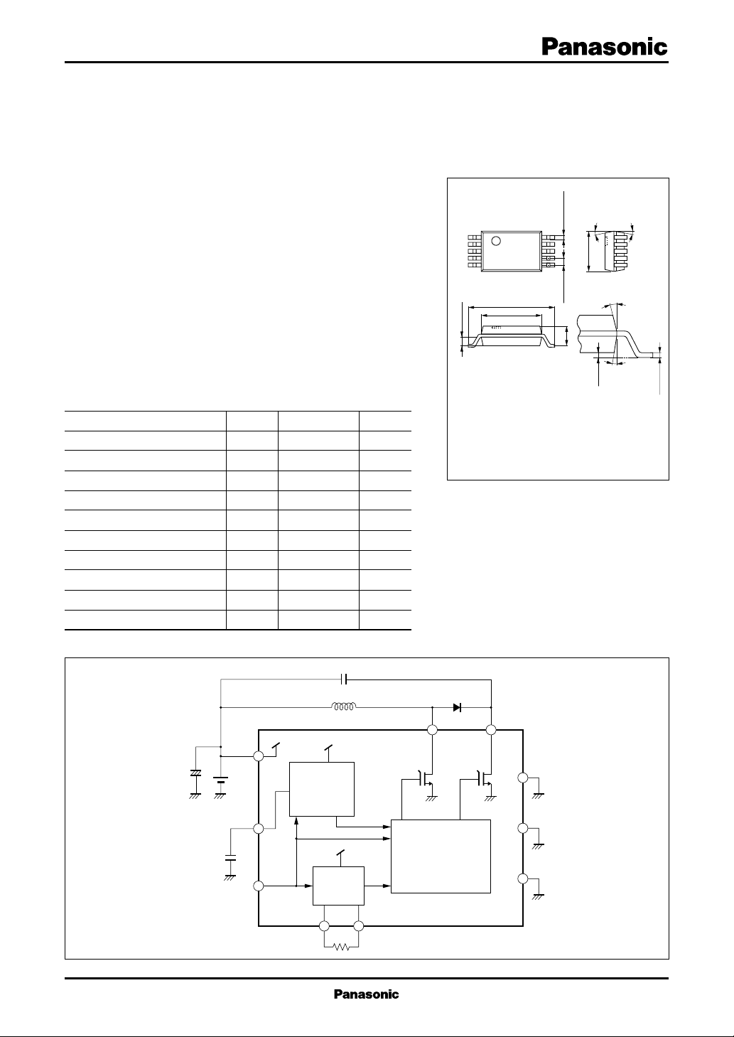
1: GND 6: V
2: GND 7: V
3: CIL8: E
4: GND 9: R
5: ELD10: R
SSONF-10D Package
unit: mm
2 to 6˚
2 to 6˚
0.15±0.05
CP
CC
NB
T1
T2
■ Block Diagram
E L
CIL
35
V
CC
V
ENB
7
Step-up circuit
CP
6
8
Oscillation
circuit
910
R
T1
R
+
-
T
R1
Logic circuit
T2
ELD
T
R2
GND
4
GND
2
GND
1
1
Intelligent Power Devices (IPDs)
MIP803, MIP804
■ Electrical Characteristics (V
Parameter
Supply voltage
Output frequency
Change of output
frequency
High level input
voltage (ENB)
Low level input
voltage (ENB)
MIP803
MIP804
MIP803
MIP804
MIP803
MIP804
MIP803
MIP804
MIP803
MIP804
Breakdown voltage
Output
(TR1)
Saturation
current
ON-state
resistance
MIP803
MIP804
MIP803
MIP804
Off-leakage current
Breakdown voltage
Output
(TR2)
Saturation
current
ON-state
resistance
MIP803
MIP804
MIP803
MIP804
Off-leakage current
Clime power the inside
voltage
Statically consumption
current
Consumption current
MIP803
MIP804
MIP803
MIP804
MIP803
MIP804
Note: ∆fv: Caluculation is made as follows:
f1 + f
∆fv = (fosc /
MIP803 f1: f
MIP804 f1: f
2
− 1) × 100
2
at VCC = 1.5V, f2: f
osc
at VCC = 0.9V, f2: f
osc
Symbol
V
CC
f
OSC
Note)
∆fv
V
IH
V
IL
V
DSS
I
DS
R
ON
I
OFF
V
DSS
I
DS
R
ON
I
OFF
V
CP
I
C
I
CC
= 2.5V/1.2V, V
CC
RT = 390kΩ
RT = 240kΩ
RT = 390kΩ
RT = 240kΩ
VCC = 1.5 to 3.5V
VCC = 0.9 to 3.3V
VCC = 1.5 to 3.5V
VCC = 0.9 to 3.3V
I
OFF(TR1)
V
DS(TR1)
I
= 10mA
DS(TR1)
V
DS(TR1)
I
OFF(TR2)
V
DS(TR2)
I
= 10mA
DS(TR2)
V
DS(TR2)
VCC = V
ENB
VCC = V
ENB
VCC = 3.5V, V
VCC = 3.3V, V
VCC = V
VCC = V
at VCC = 3.5V
osc
at VCC = 3.5V
osc
= 2.5V/1.2V, GND = 0, TC = 25 ± 2°C)
ENB
Conditions
= 0.1mA
= 20V
= 160V
= 0.1mA
= 20V
= 160V
= 1.5V, CCP = 1000pF, RT = 390kΩ
= 0.9V, CCP = 1000pF, RT = 240kΩ
= 0
ENB
= 0
ENB
= 3.5V, RT = 390kΩ
ENB
= 3.3V, RT = 240kΩ
ENB
min
1.5
0.9
119
195
−7
−15
1
0.8
200
70
60
200
15
10
0.5
0.7
2
2
typ
2.5
140
230
6.5
0.75
1
1
1
max
3.5
3.5
161
265
7
15
0.3
0.1
10
15
2
1
1.4
2
0.1
0.1
1.5
1.5
Unit
V
kHz
%
V
V
V
mA
Ω
µA
V
mA
kΩ
µA
V
µA
mA
■ Pin Descriptions
Pin No.
1
2
3
4
5
6
7
8
9
10
2
Symbol
GND
GND
C
IL
GND
E
LD
V
CP
V
CC
E
NB
R
T1
R
T2
Pin Name
GND pin
GND pin
Output for voltage step-up
GND pin
Output for EL driving
Internal voltage step-up pin
Power input pin
ENABLE pin
Internal oscillation output
OSC resistor connecting pin
GND pin
GND pin
Drain pin of the voltage step-up MOS FET
GND pin
Drain pin of the EL drive MOS FET
Capacitor connection pin for internal voltage step-up power supply
Power input pin
ENABLE signal input pin for controlling the EL driver (if ENB = H, the EL
driver becomes ON and if ENB = L/OPEN, it becomes OFF)
Internal oscillation circuit output pin
OSC resistor connection pin for connecting the OSC resistor between RT1 and R
Description
T2
 Loading...