

Panasonic MIP704 Datasheet
Intelligent Power Devices (IPDs)
MIP704
Silicon MOS IC
■ Features
●3-pin intelligent power device
●Five protective functions (over-current, over-voltage, short circuit
load, over heat, ESD) are integrated
●Acceptable both AC and DC power supply
■ Applications
●For automotive electric equipment
■ Absolute Maximum Ratings (Ta = 25°C)
Parameter
Drain to Source voltage
Output peak current
Output current
Input voltage
Input current
Drain clamp energy
Allowable power dissipation
Operating ambient temperature
Channel temperature
Storage temperature
1
*
Maximum load current, not the average current.
2
*
L = 10mH, IL = 3.32A, VDD = 30V, 1pulse, TC = 85°C
3
*
Mounting on the PCB (Glass epoxy board, the size of 100mm × 100mm). (Ta = 25°C)
Symbol
V
DS
I
OP
I
O
V
IN
I
IN
EAS
P
D
T
opr
T
ch
T
stg
Ratings
60
±5
1
*
−1 to 2
− 0.5 to 6
±10
2
*
55
3
*
1
−40 to +85
150
−55 to +150
Unit
V
A
A
V
mA
mJ
W
°C
°C
°C
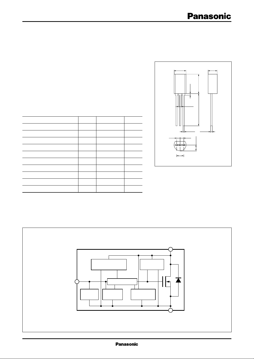
1.27
5.0±0.2
123
2.54±0.15
0.7±0.2
0.7±0.1
0.45
1.27
8.0±0.2
13.5±0.5
+0.15
–0.1
0.45
2.3±0.2
TO-92 NL Package
+0.15
–0.1
unit: mm
4.0±0.2
1: Source
2: Drain
3: IN
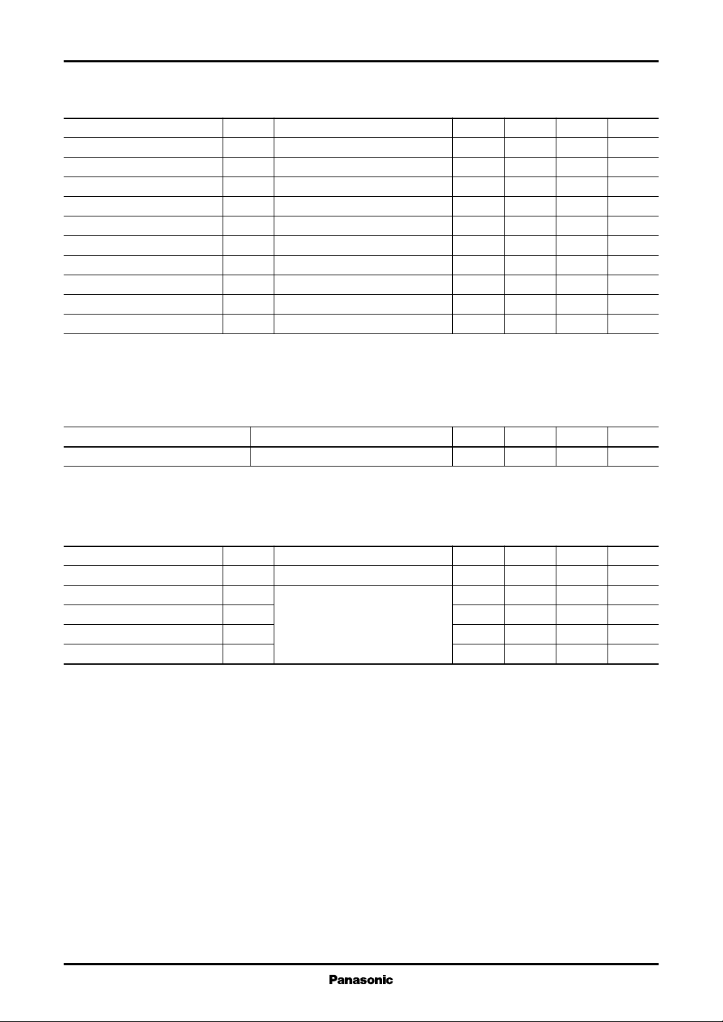
■ Block Diagram
IN
ESD
protection
Short circuit load
protection
Gate cut-off circuit
Over heat
protection
D
Over voltage
protection
Over current
protection
S
1
Intelligent Power Devices (IPDs)
MIP704
■ Electrical Characteristics (T
Parameter
Drain to Source ON-resistance
Drain to Source ON-voltage
Drain clamp voltage
Drain OFF current (1)
Drain OFF current (2)
Input voltage (High)
Input voltage (Low)
Input current
Over current protection limit
Short circuit load protection limit
C
Symbol
R
DS(on)
V
DS(on)
V
DS(CLP)
I
DS(off)1
I
DS(off)2
V
IN(H)
V
IN(L)
I
IN(on)
I
OCP
V
DS(SHT)
= 25 ± 2°C)
VIN = 5V, IDS = 1.5A
VIN = 5V, IDS = 1.5A
VIN = 0, IDS = 3mA
VIN = 0, VDS = 12V
VIN = 0, VDS = 16V
IDS = 2A
IDS = 1mA
VIN = 5V, VDS = 0
VIN = 5V, VDS = 3V
VIN = 5V
Conditions
min
60
4
3.8
3
typ
0.38
0.57
72
50
65
0.15
5
4
max
0.5
0.75
80
140
0.8
0.5
Unit
Ω
V
V
µA
µA
V
V
mA
A
V
Note: The oscillation of the output current is caused when the drain voltage exceeds the short circuit load detection voltage under
the ON state of output.
■ Operating condition
Parameter
Operating supply voltage
V
DD
Symbol
min typ max
40
Unit
V
■ Electrical Characteristics (T
Parameter
Over heat protection temperature
Turn on delay time
Rise time
Turn off delay time
Fall time
C
Symbol
T
SHD
t
d(on)
t
r
t
d(off)
t
f
= 25 ± 2°C)
VIN = 5V
VIN = 5V, IDS = 1.5A
VDD = 12V, RL = 8.2Ω
Conditions
min
170
typ
205
3
18
12
20
Note 1: The above values of characteristics are not guaranteed values and are only references for designing.
Note 2: If the chip temperature exceeds the "Over Heat Protection Temperature", output current is shut down.
max
240
Unit
°C
µs
µs
µs
µs
2
 Loading...