Panasonic MIP506 Datasheet

Intelligent Power Devices (IPDs)
MIP506
Silicon MOS IC
■ Features
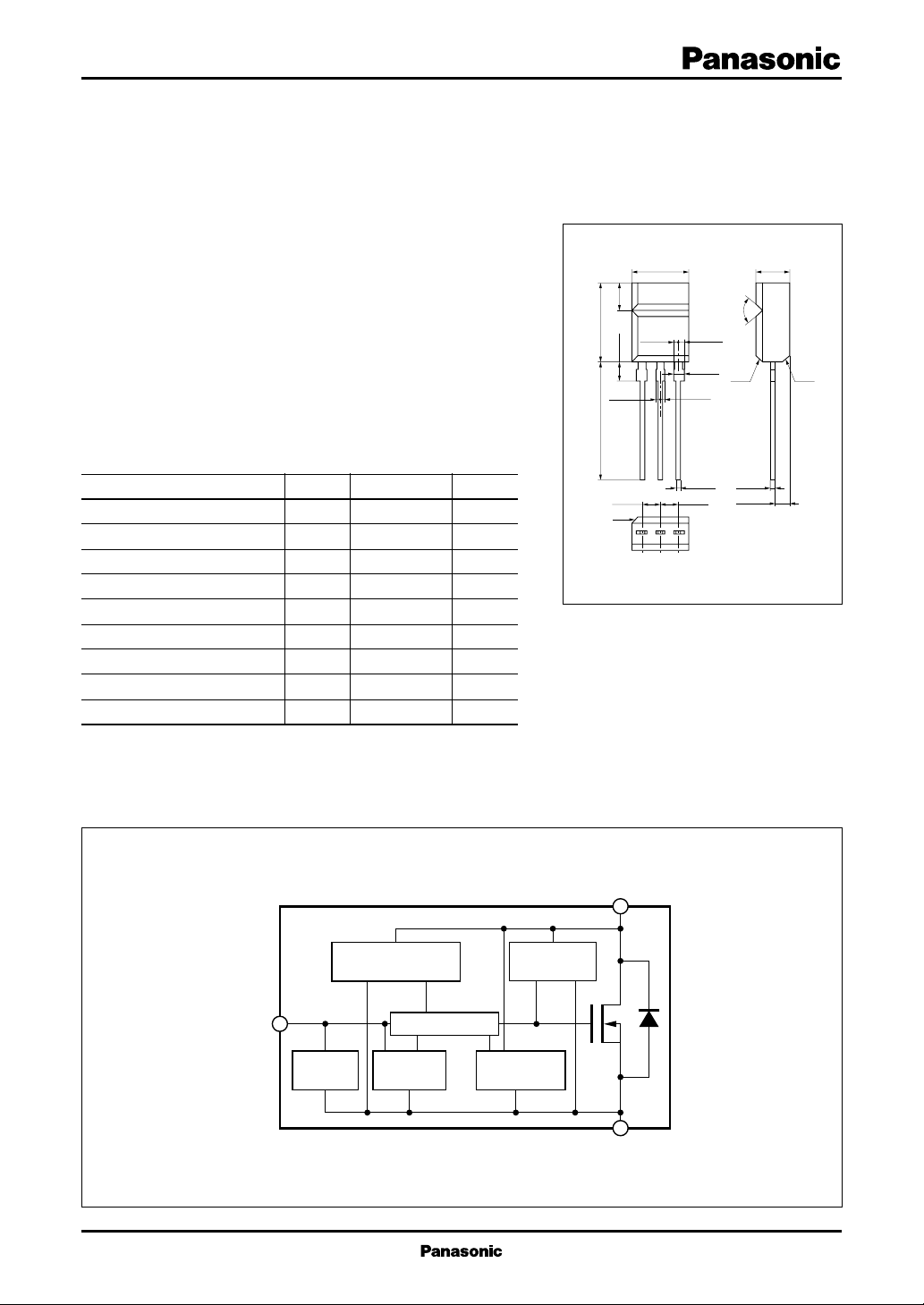
●3-pin intelligent power device
●Five protective functions (over-current, over-voltage, short circuit
load, over heat, ESD) are integrated
●Acceptable both AC and DC power supply
■ Applications
●For lamp and solenoid drive
■ Absolute Maximum Ratings (Ta = 25°C)
Parameter
Drain to Source voltage
Output peak current
Output current
Input voltage
Input current
Allowable power dissipation
Operating ambient temperature
Channel temperature
Storage temperature
Symbol
V
DS
I
OP
I
O
V
IN
I
IN
P
D
T
opr
T
ch
T
stg
Ratings
45
±7.5
2
− 0.5 to 6
±10
1.5
−40 to +85
150
−55 to +150
Unit
V
A
A
V
mA
W
°C
°C
°C
7.5±0.2 4.5±0.2
3.8±0.2
10.8±0.216.0±1.0
2.5±0.1
0.7±0.1
0.8C
123
0.7±0.1
0.5±0.1
2.5±0.22.5±0.2
90˚
0.85±0.10.65±0.1
1.0±0.1
unit: mm
0.8C
0.4±0.1
2.05±0.2
MT3 Type Package
0.8C
1: IN
2: Drain
3: Source
■ Block Diagram
IN
Short circuit load
ESD
protection
protection
Gate cut-off circuit
Over heat
protection
D
Over voltage
protection
Over current
protection
S
1

Intelligent Power Devices (IPDs)
MIP506
■ Electrical Characteristics (T
Parameter
Drain to Source ON-resistance
Drain to Source ON-voltage
Drain clamp voltage
Drain OFF current (1)
Drain OFF current (2)
Drain OFF current (3)
Input voltage (High)
Input voltage (Low)
Input current
Over current protection limit
Short circuit load protection limit
C
Symbol
R
DS(on)
V
DS(on)
V
DS(CLP)
I
DS(off)1
I
DS(off)2
I
DS(off)3
V
IN(H)
V
IN(L)
I
IN(on)
I
OCP
V
DS(SHT)
= 25 ± 2°C)
VIN = 5V, IDS = 1.5A
VIN = 5V, IDS = 1.5A
VIN = 0, IDS = 3mA
VIN = 0, VDS = 12V
VIN = 0, VDS = 25V
VIN = 0, VDS = 40V
IDS = 1.5A
IDS = 0.1mA
VIN = 5V, VDS = 0
VIN = 5V
VIN = 5V
Conditions
min
45
4.5
4.7
2
typ
0.21
0.32
55
0.15
7.5
max
0.3
0.45
30
60
100
0.8
0.5
Unit
Ω
V
V
µA
µA
µA
V
V
mA
A
V
Note: The oscillation of the output current is caused when the drain voltage exceeds the short circuit load detection voltage under
the ON state of output.
■ Electrical Characteristics (T
Parameter
Over heat protection temperature
Temperature hysteresis
C
Symbol
T
SHD
∆T
= 25 ± 2°C)
VIN = 5V
VIN = 5V
Conditions
min typ
140
30
max Unit
°C
°C
Note 1: The above values of characteristics are not guaranteed values and are only references for designing.
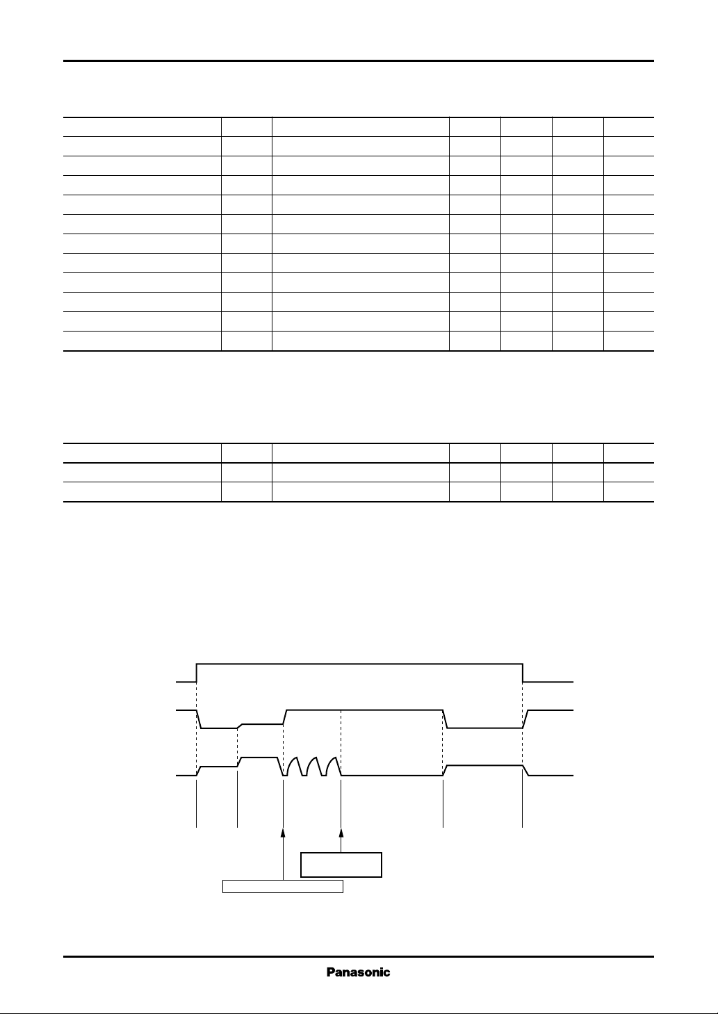
Note 2: When the chip surface temperature exceeds the over heat protection temperature, the output current is shut down. After
the chip surface temperature is lowered by an equivalent degree of the temperature hysteresis, the circuits restart their
operation.
■ Timing Chart
V
V
I
DS
2
IN
DS
ON
state
current
limiting
state
Detecting short circuit load
Short circuit
load state
Over heat protection
operating state
Detecting over
heat
ON state OFF stateOver
(Temperature
hysteresis)
 Loading...