

Panasonic MIP301 Datasheet
Intelligent Power Devices (IPDs)
MIP301
Silicon MOS IC
■ Features
●100V high breakdown voltage MOS FET and CMOS control cir-
cuits are integrated into one chip
●5V and 3 - 5W output with 24VDC input (Flyback method)
■ Applications
●IPD for DC/DC converter
■ Absolute Maximum Ratings (Ta = 25 ± 3°C)
Parameter
Drain voltage
Control voltage
Input voltage
Output current
Control current
Channel temperature
Storage temperature
Symbol
V
D
V
C
V
IN
I
D
I
C
T
ch
T
stg
Ratings
90
8
30
1.1
0.1
150
−55 to +150
Unit
V
V
V
A
A
°C
°C
0.6±0.3
1.27
0.1±0.1
0.3
0.4±0.25
1
2
3
4
4.2±0.3
6.5±0.3
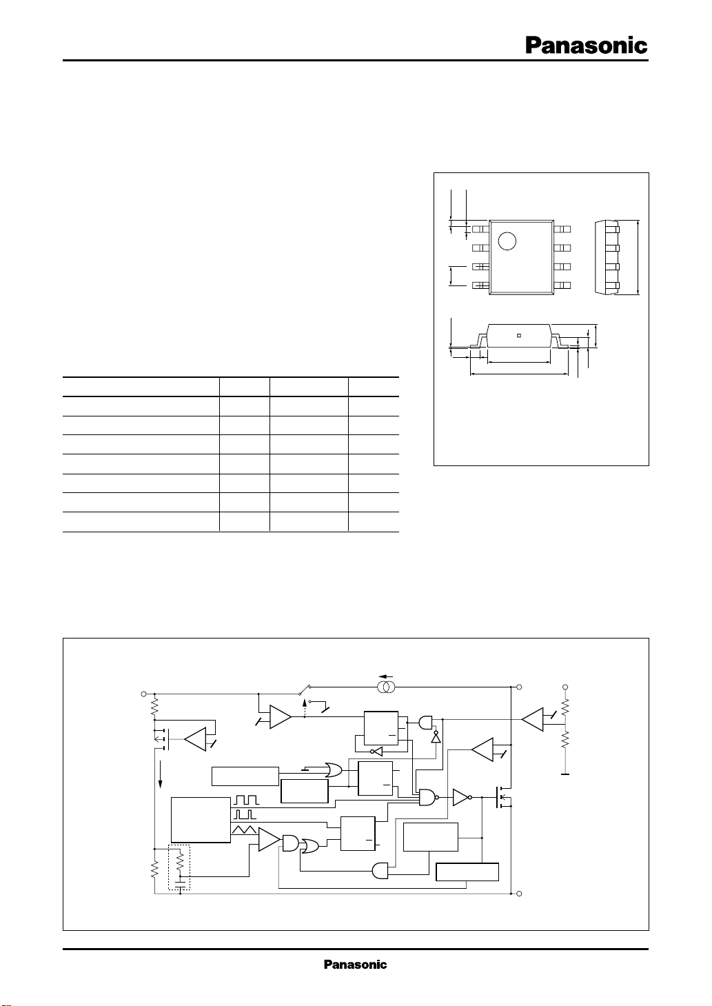
unit: mm
8
7
6
5
1.5±0.2
0.65
0.2±0.1
1: VIN 5: Drain
2: Source 6: Source
3: Source 7: Source
4: Control 8: Source
SO-8P Type Package
5.0±0.3
■ Block Diagram
Control pin Shutdown/Auto-restart
Shunt
regulator
PWM control
current
Max Duty
Sawtooth
+
Thermal shutdown
Clock
Low pass filter
5.7V
4.7V
circuit
+
+
-
Restarting
trigger circuit
Auto-restart
0
1
Power supply
for internal
circuit
S
R
S
R
Auto-restart current-source
D
T
Q
R
Q
Q
Q
Q
Q
Leading edge
blanking
Drain pin
R
X I
on
Power
MOS FET
Minimum ON-time
delay circuit
Source pin
V
IN
-
D
+
-
+
1
Intelligent Power Devices (IPDs)
MIP301
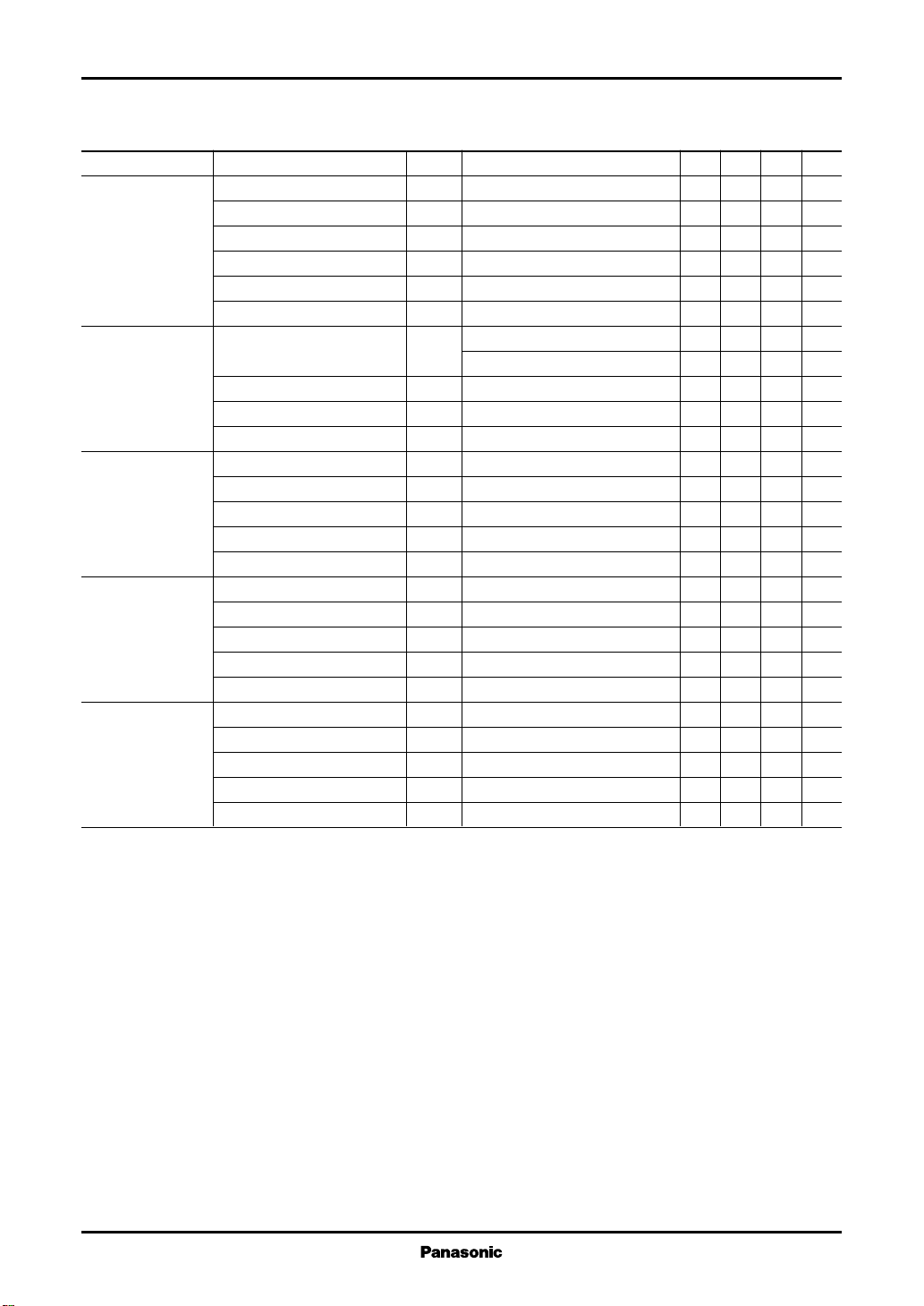
■ Electrical Characteristics (T
Parameter
Output frequency
Maximum duty cycle
Control functions
Auto-restart
Circuit protection
Output
Power supply voltage
Minimum duty cycle
PWM gain
Circuit current
Dynamic impedance
Control pin charging current
Auto-restart threshold voltage
Lockout threshold voltage
Auto-restart hysteresis voltage
Self-protection current limit
Leading edge blanking delay
Current limit delay
Thermal shutdown temperature
Power-up reset threshold voltage
ON-state resistance
OFF-state current
Breakdown voltage
Rise time
Fall time
Start threshold voltage
Stop threshold voltage
Input hysteresis voltage
Shunt regulator voltage
Control supply/discharge current
= 25 ± 2°C)
C
Symbol
f
OSC
MAXDC
MINDC
GPWM
Is
ZC
I
C
V
C(on)
V
C(off)
∆V
C
I
LIMIT
t
on(BLK)
t
d(OCL)
T
OTP
V
C reset
R
DS(on)
I
DSS
V
DSS
t
r
t
f
V
IN(START)
V
IN(STOP)
∆V
IN
V
C
I
CD
Conditions
IC = 2mA
IC = 2mA
IC = 10mA
IC = 3mA
VC = 0
VC = 5V
IC = 3mA
IC = 3mA
IC = 3mA
ID = 1A
VDS = 82V Output MOS FET disabled
ID = 0.25mA Output MOS FET disabled
IC = 3mA
Output MOS FET disabled
min
180
77
0
−21
0.8
10
−2.4
−2
5
4
0.5
0.9
130
2.3
92
16
10
5.5
5.4
0.5
typ
200
80
3
−16
2.5
15
−1.9
−1.5
5.7
4.7
1
1
0.25
0.1
140
3.3
1.8
0.01
0.1
0.1
5.7
0.8
max
220
83
5
−11
4
25
−1.2
− 0.8
6.3
5.3
1.5
1.1
150
4.2
2.2
0.25
0.2
0.2
18.2
12.2
7.5
6.1
1.1
Unit
kHz
%
%
%/mA
mA
Ω
mA
mA
V
V
V
A
µs
µs
°C
V
Ω
mA
V
µs
µs
V
V
V
V
mA
2
 Loading...