

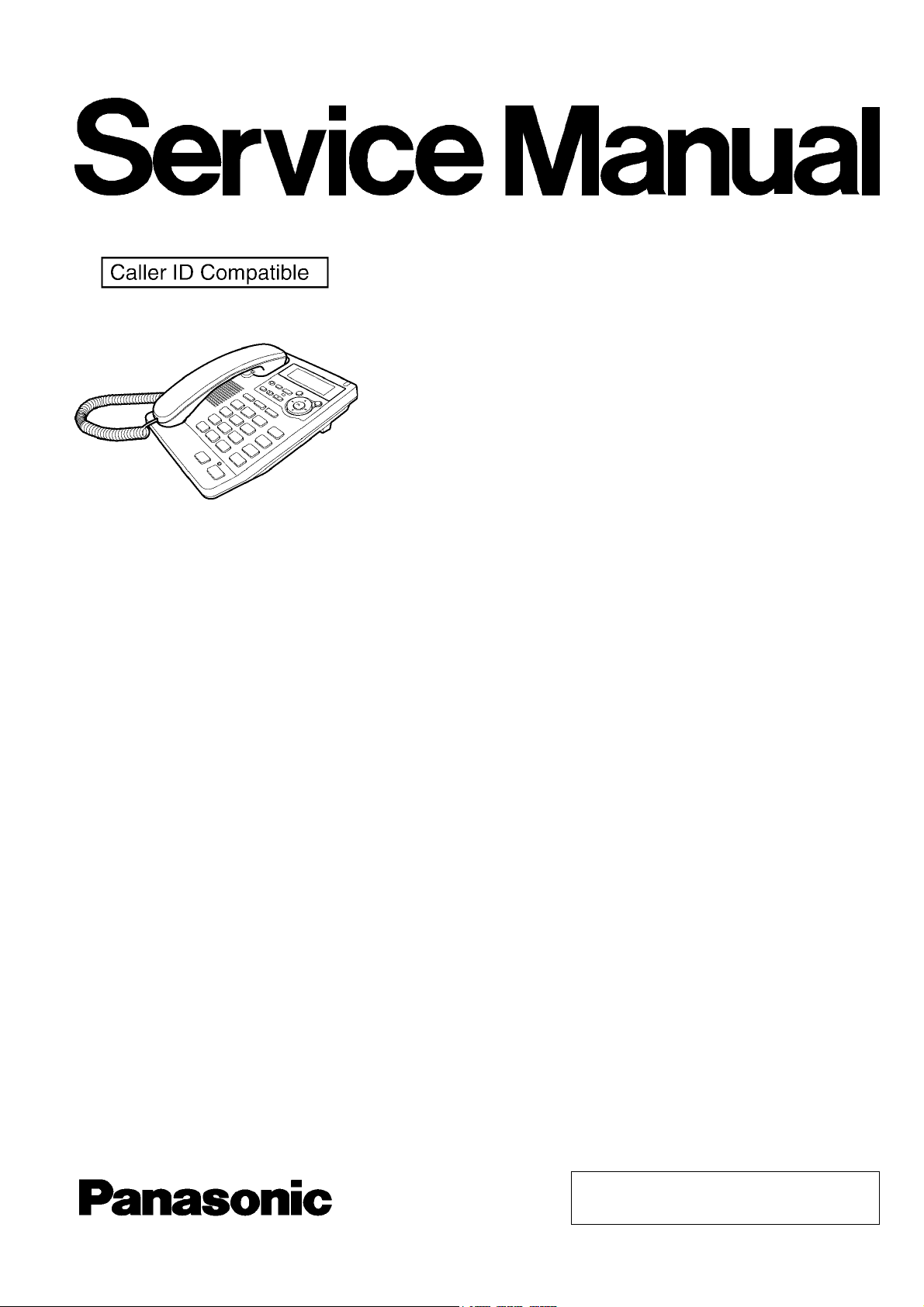
Panasonic KX-TS2570UAB, KX-TS2570UAW Service manual
ORDER NO. KM40609202CE
Telephone Equipment
KX-TS2570UAB
KX-TS2570UAW
Telephone Answering System
Black Version
White Version
(for Ukraine)
© 2006 Panasonic Communications Co., Ltd. All
rights reserved. Unauthorized copying and distribution is a violation of law.
KX-TS2570UAB/KX-TS2570UAW
2

TABLE OF CONTENTS
PAGE PAGE
1 Safety Precaution ------------------------------------------------ 4
1.1. For Service Technicians --------------------------------- 4
2 Warning-------------------------------------------------------------- 4
2.1. About Lead Free Solder (Pbf: Pb free)--------------- 4
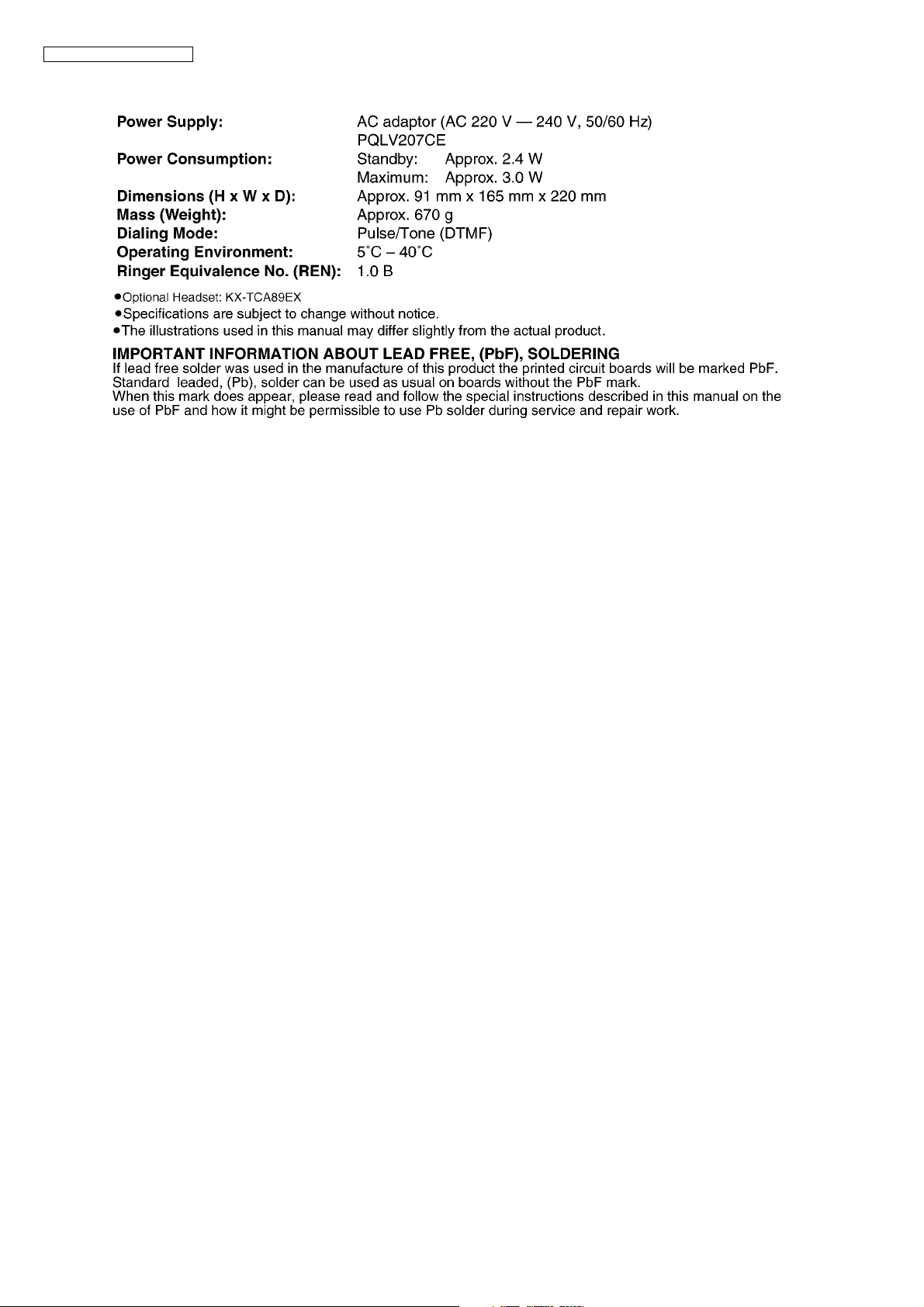
3 Specifications ----------------------------------------------------- 6
4 Technical Descriptions----------------------------------------- 7
4.1. Block Diagram (Base Unit)------------------------------ 7
4.2. Circuit Operation (Base Unit)--------------------------- 8
4.3. Ringer IC----------------------------------------------------10
4.4. Module Block Diagram ---------------------------------- 11
4.5. Signal Route -----------------------------------------------12
5 Location of Controls and Components ------------------13
5.1. Controls -----------------------------------------------------13
6 Installation Instructions---------------------------------------15
6.1. Connections------------------------------------------------15
7 Operation Instructions-----------------------------------------17
7.1. Dial Lock ----------------------------------------------------17
7.2. Troubleshooting-------------------------------------------18
8 Service Mode -----------------------------------------------------20
8.1. How to Clear User Setting------------------------------20
9 Troubleshooting Guide----------------------------------------21
9.1. Troubleshooting Guide----------------------------------21
9.2. How to Replace the Flat Package IC ----------------28
10 Disassembly and Assembly Instructions ---------------30
11 Schema tic D i agra m ---------------------------------------------31
11.1. For Schematic Diagram---------------------------------31
11.2. Schematic Diagram (Main)-----------------------------32
11.3. Schematic Diagram (Operation) ----------------------34
12 Printed Circuit Board-------------------------------------------35
12.1. Circuit Board (Main)--------------------------------------35
12.2. Circuit Board (Operation)-------------------------------37
13 Appendix Information of Schematic Diagram ---------39
13.1. CPU Data --------------------------------------------------39
13.2. Terminal Guide of the Ics, Transistor and
Diodes-------------------------------------------------------41
14 Exploded View and Replacement Parts List -----------42
14.1. Cabinet and Electric Parts -----------------------------42
14.2. Accessories and Packing Materials------------------43
14.3. Replacement Part List-----------------------------------44
KX-TS2570UAB/KX-TS2570UAW
3
KX-TS2570UAB/KX-TS2570UAW
1 Safety Precaution
1.1. For Service Technicians
ICs and LSIs are vulnerable to static electricity.
When repairing, the following precautions will help prevent recurring malfunctions.
1. Cover the plastic parts boxes with aluminum foil.
2. Ground the soldering irons.
3. Use a conductive mat on the worktable.
4. Do not touch IC or LSI pins with bare fingers.
2Warning
2.1. About Lead Free Solder (Pbf: Pb free)
Note:
In the information below, Pb, the symbol for lead in the periodic table of elements, will refer to standard solder or solder that contains lead.
We will use PbF solder when discussing the lead free solder used in our manufacturing process which is made from Tin (Sn),
Silver (Ag), and Copper (Cu).
This model, and others like it, manufactured using lead free solder will have PbF stamped on the PCB. For service and repair
work we suggest using the same type of solder.
Caution
• PbF solder has a melting point that is 50 °F ~ 70 °F (30 °C ~ 40 °C) higher than Pb solder. Please use a soldering iron with
temperature control and adjust it to 700 °F ± 20 °F (370 °C ± 10 °C).
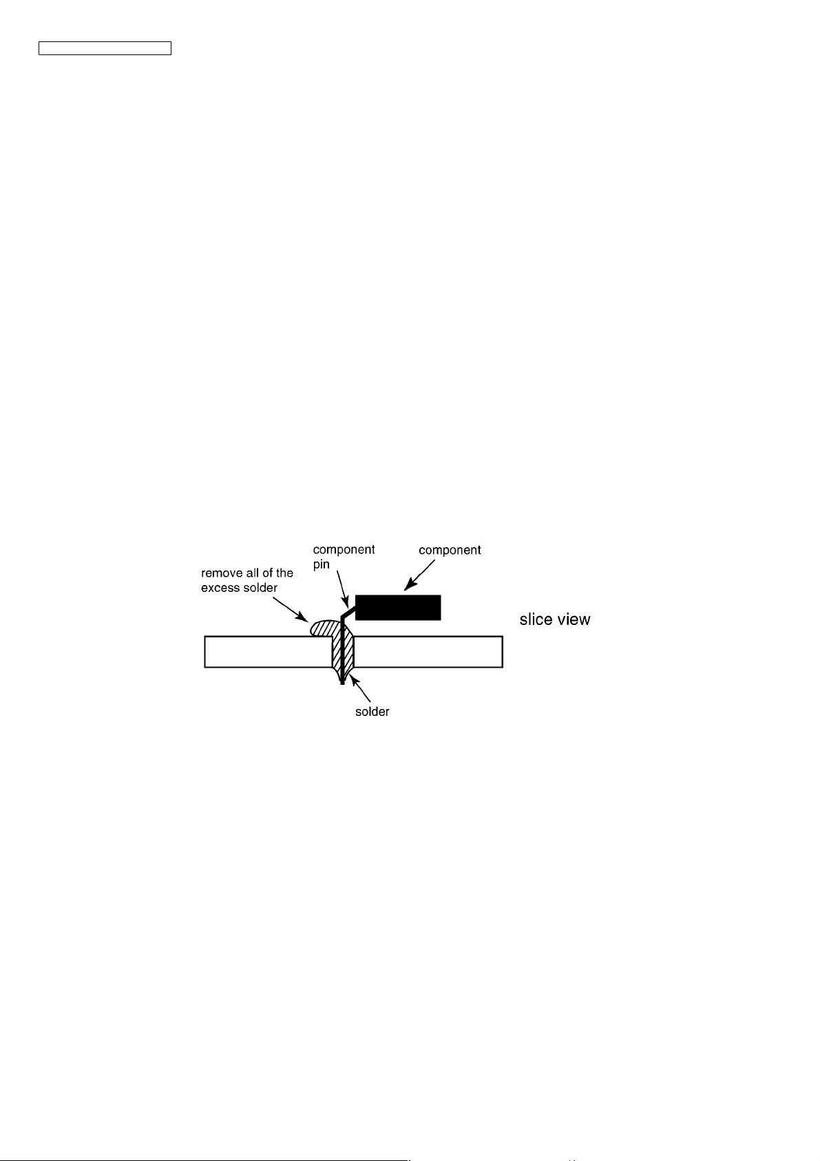
• Exercise care while using higher temperature soldering irons.:
Do not heat the PCB for too long time in order to prevent solder splash or damage to the PCB.
• PbF solder will tend to splash if it is heated much higher than its melting point, approximately 1100 °F (600 °C).
• When applying PbF solder to double layered boards, please check the component side for excess which may flow onto the
opposite side (See the figure below).
4
KX-TS2570UAB/KX-TS2570UAW
2.1.1. Suggested PbF Solder
There are several types of PbF solder available commercially. While this product is manufactured using Tin, Silver, and Copper
(Sn+Ag+Cu), you can also use Tin and Copper (Sn+Cu) or Tin, Zinc, and Bismuth (Sn+Zn+Bi). Please check the manufac
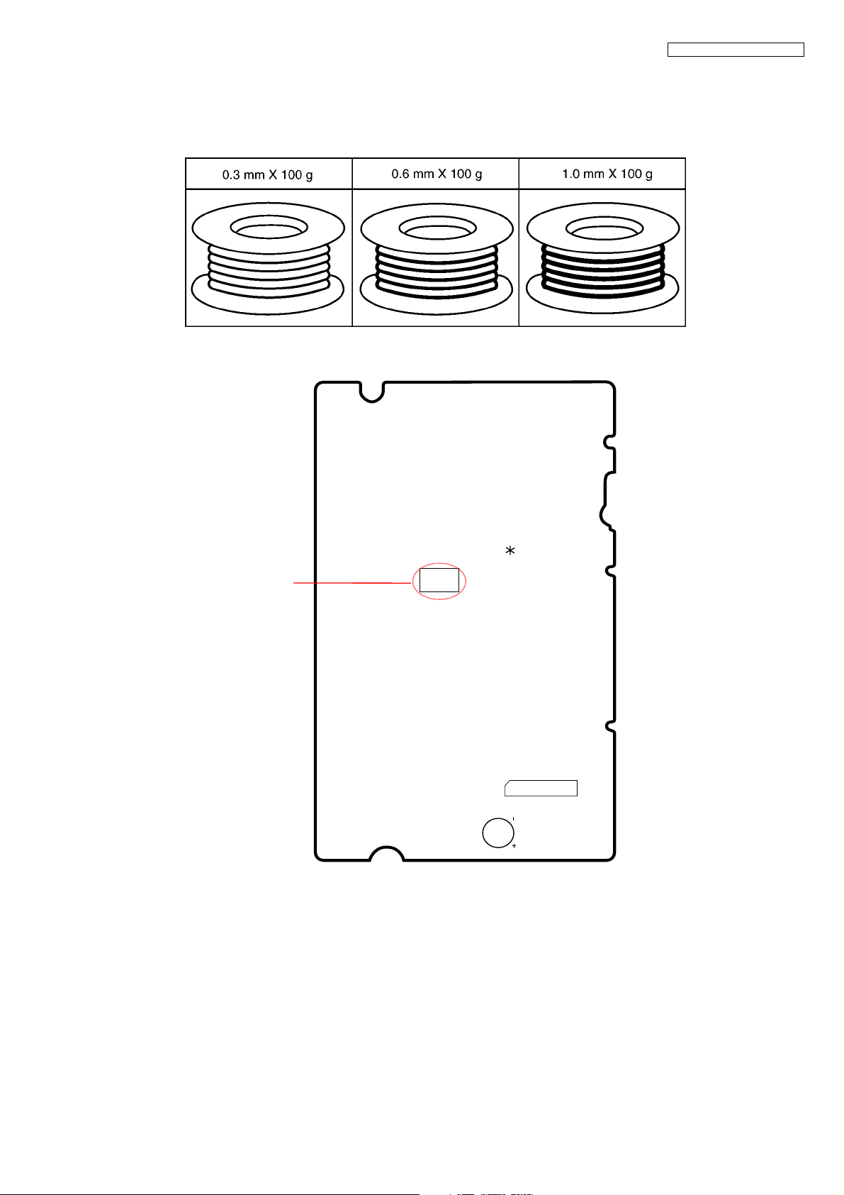
turer’s specific instructions for the melting points of their products and any precautions for using their product with other materials. The following lead free (PbF) solder wire sizes are recommended for service of this product: 0.3 mm, 0.6 mm and 1.0 mm.
2.1.2. How to recognize that Pb Free solder is used
(Example: Operation P.C.B.)
Marked
(Component View)
Note:
The location of the “PbF” mark is subject to change without notice.
PQUP11371Z
PbF
17
18
MIC
CN801
1
2
A
5
KX-TS2570UAB/KX-TS2570UAW
3 Specifications
6

4 Technical Descriptions
4.1. Block Diagram (Base Unit)
T
R
KX-TS2570UAB/KX-TS2570UAW
R1
IC
RINGER
PC1
Ringer indication LED
LED 804 (1AP - SUB)
IC1 D4, D6
D7, D9
Line
Q103, Q104
Q108
Sidetone
Handset
ON/OFF
Bridge
Amp
Sending
V
D304
6.5V
DC Power
IC303, Q301
4.0V
4.0V
Regulator
Reg.
IC304
3.2V
Regulator
IC305
IC903
Power Down
Detection
Reset IC
Q701 Q702
1.8V
D306
Reg.
Q401 D8, D10
KX-TS2570 BLOCK DIAGRAM
T1 D3, D5 C1
Handset / Headset
Speaker
2AP
MIC
SP
Headset
Detection
Q402
IC904
IC902
Amp
SP-Phone
MIC
LSR +
MIC -
Switch
Keyboard
LSR -
MIC +
LINE IN -
HeadsetDET
LINE OUT
FLASH
MEMORY
LCD
RSTn
VDDIO
VBAT2
VDD, AVD
IC901
DSP MICON
NS BBIC
BELL
ACFL
CIDIN+
CIDIN -
JOHN SMITH
1234567890
7
KX-TS2570UAB/KX-TS2570UAW
4.2. Circuit Operation (Base Unit)
4.2.1. Outline
The unit consists of the following ICs as shown in the BLOCK DIAGRAM
• BBIC (Base Band IC): IC901
- Handling all the audio, signal and data processing needed
- ADPCM codec filter for speech encoding and speech decoding (DSP section)
- Echo-cancellation and Echo-suppression (DSP section)
- Any tones (tone, sidetone, ringing tone, etc.) genereation (DSP section)
- DTMF receiver (DSP section)
- ADC, DAC, timer and power control circuitry
- All interfaces (eg: LCD, LED, Analog Front End, etc.)
• FLASH MEMORY : IC902
- Voice Prompt (TAM) Download Area
- Program D/L Area
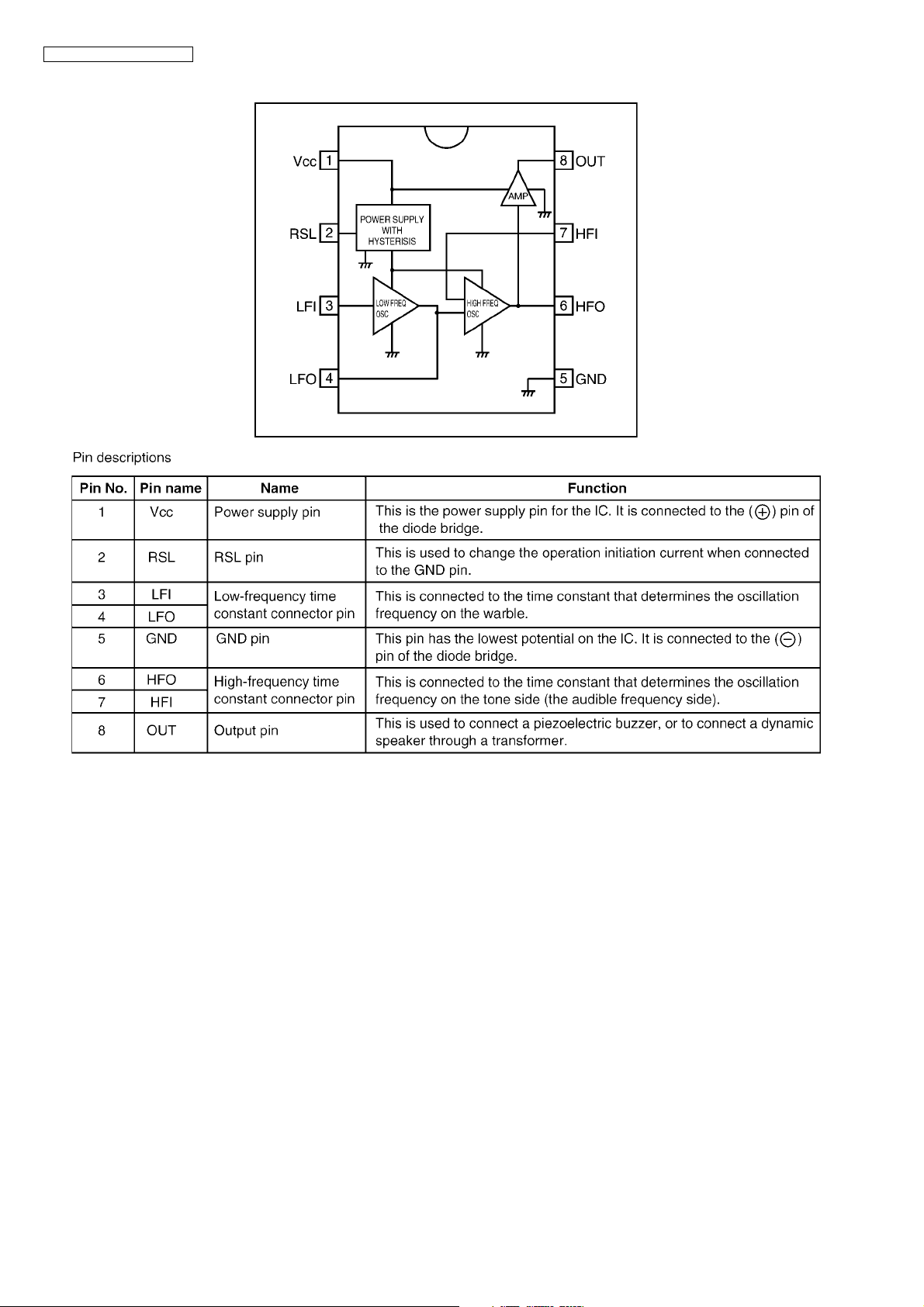
• RINGER IC : IC1
- Bell signal generator (for bell detection purpose)
• SP AMP : IC904
- Low voltage audio power amplifier
• Additionally,
- Power Supply Circuit (+4.0V, +4.0V, +3.2V, +1.8V output)
- Telephone Line Interface Circuit
- Bell Detection Circuit
- SP-Phone Circuit
- Handset Circuit
-TAM Circuit
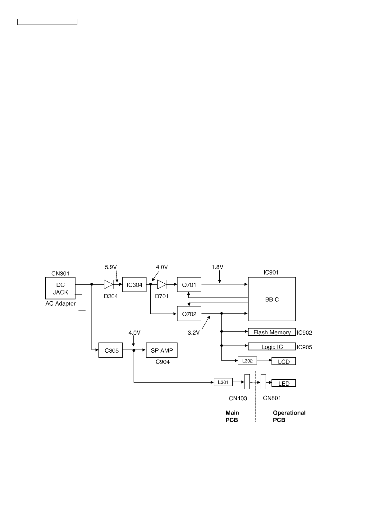
4.2.2. Power Supply Circuit
The power is supplied to the BBIC, Flash ROM, SP AMP, Logic IC, LCD, LED from AC adaptor (6.5V)
as below :
• BBIC (IC901) : CN301 (+6.5V) -> D304 -> IC304 -> Q702 -> IC901 (3.2V)
• BBIC (IC901) : CN301 -> D304 ->IC304 -> D701 -> Q701 -> IC901 (1.8V)
• Flash Memory (IC902) : CN301(+6.5V) -> D304 -> IC304 -> Q702 -> IC902
• Logic IC (IC905) : CN301(+6.5V) -> D304 -> IC304 -> Q702 -> IC904
• SP AMP (IC904) : CN301(+6.5V) -> IC305 -> IC904
• LCD (LCD) : CN301(+6.5V) -> D304 -> IC304 -> Q702 -> L302 -> LCD
• LED (LED801, LED802) : CN301(+6.5V) -> IC305 -> L301 -> CN403 -> CN801 -> LED
8

KX-TS2570UAB/KX-TS2570UAW
4.2.3. Telephone Line Interface
• Bell Signal Detection
• Caller ID Detection
• ON/OFF hook Circuit
•Audio Circuit
4.2.3.1. Bell Detection Circuit
When the bell signal is input from LINE to T/R (when the telephone rings), BBIC detects bell signal via following path :
T -> D3 -> IC1(1) -> IC1(8) -> C4 -> R6 -> PC1(1) -> PC1(4) -> IC901(63)
R -> R1 -> LED804 -> D4 -> IC1(1) -> IC1(8) -> C4 -> R6 -> PC1(1) -> PC1(4) -> IC901(63)
After bell signal detected at IC901(63), the bell ringing signal is output at the speaker via the following path :
4.2.3.2. Caller ID Detection Circuit
Normally, FSK caller ID data is followed after the 1st bell signal.
When the bell signal is detected by BBIC, Caller ID signal is sent through the circuit via
following path :
T -> C501 -> R503 -> R905 -> IC901(107)
R -> C502 -> R504 -> R908 -> IC901(112)
4.2.3.3. On/Off Hook Circuit
In standby mode, SW101 is open and Q104 is OFF. Consequently Q103 is open and cut the DC loop current and voice signal.
This is an on-hook condition.
When handset is picked up or SP-Phone key is pressed, Q104 turns on and then Q103 turns on, thus providing an off-hook condition. A DC loop is made and current flows through the circuit via following path :
T -> D7 -> Q103 -> Q108 -> R124 -> D106 -> D10 -> R
Pulse signal is generated by repeated switches between high (3.2V) and low (0V) logic output from IC901(79), switching the line
loop on and off.
4.2.3.4. Handset Circuit
* Refer to Signal Route
4.2.3.5. Speakerphone Circuit
* Refer to Signal Route
9
KX-TS2570UAB/KX-TS2570UAW
4.3. Ringer IC
10

4.4. Module Block Diagram
4.4.1. LCD Module Block
4.4.2. Connector Pin Assignment
Pin no. Signal Function Enable
1 VDD +3V Power Supply —
2 VSS 0V Power Supply —
3 DB4 Data Bus Line H/L
4 DB5 Data Bus Line H/L
5 DB6 Data Bus Line H/L
6 DB7 Data Bus Line H/L
7 R/W Read / Write H/L
8 E Enable Signal H
9 D/C Data / Command Control H/L
10 CS Chip Signal L
11 RES Reset Signal Input L
KX-TS2570UAB/KX-TS2570UAW
11

KX-TS2570UAB/KX-TS2570UAW
4.5. Signal Route
12

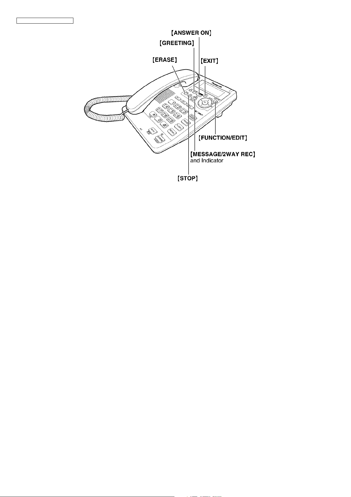
5 Location of Controls and Components
5.1. Controls
KX-TS2570UAB/KX-TS2570UAW
13
KX-TS2570UAB/KX-TS2570UAW
14
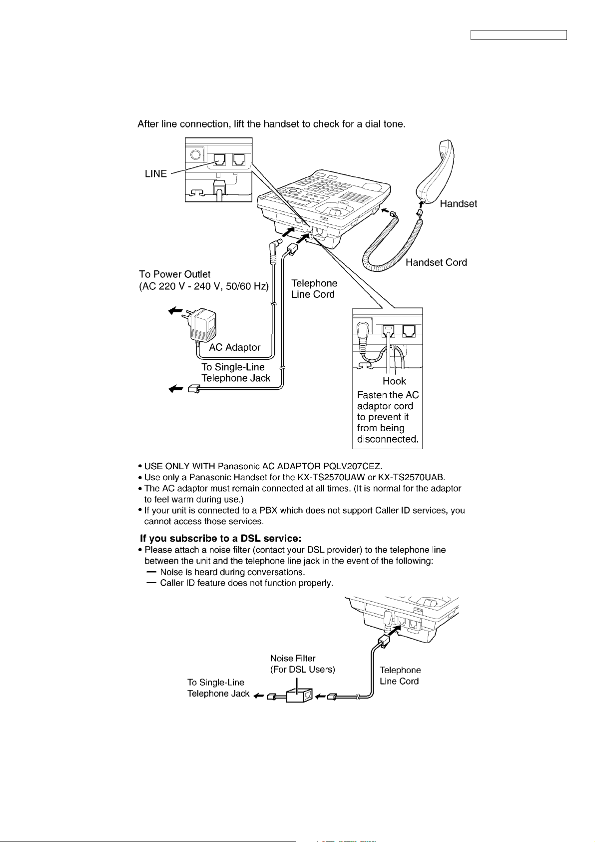
6 Installation Instructions
6.1. Connections
6.1.1. Connecting the Handset/AC Adaptor/Telephone Line Cord
KX-TS2570UAB/KX-TS2570UAW
15
 Loading...