

ORDER NO. KM40609202CE
Telephone Equipment
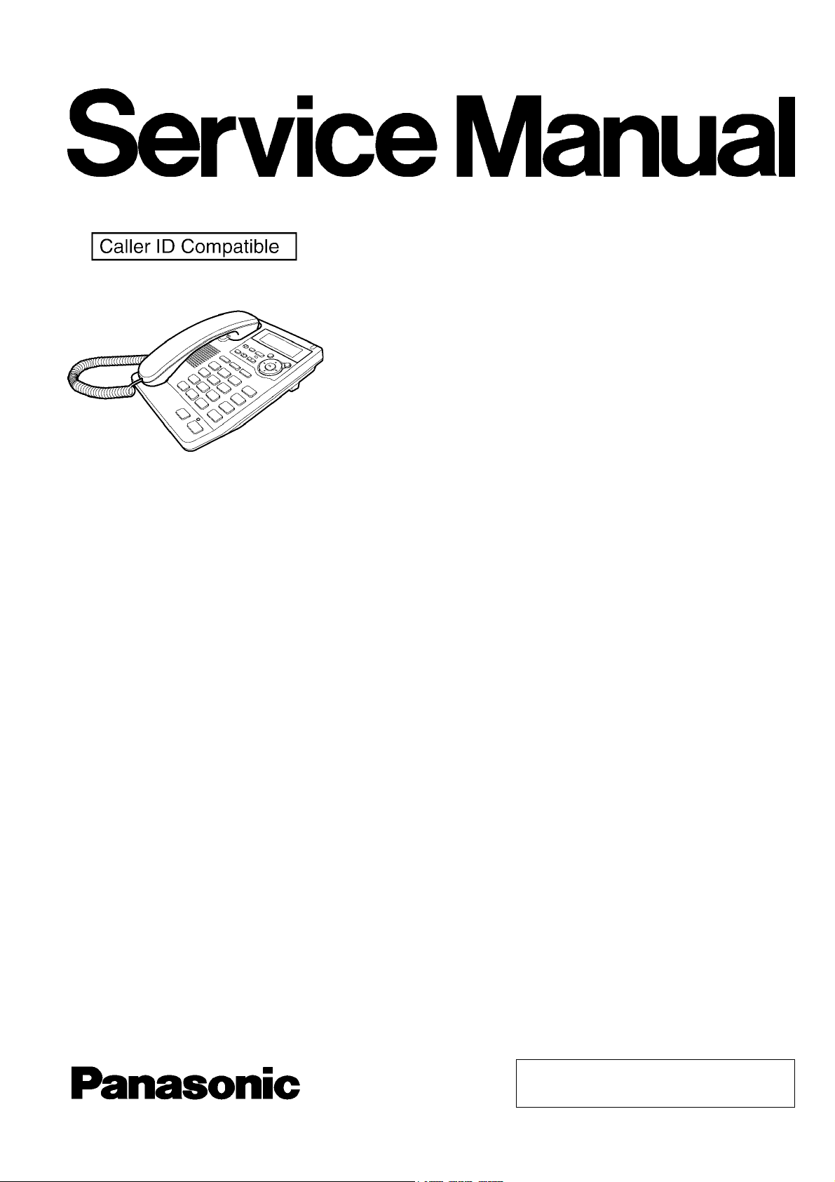
KX-TS2570UAB
KX-TS2570UAW
Telephone Answering System
Black Version
White Version
(for Ukraine)
© 2006 Panasonic Communications Co., Ltd. All
rights reserved. Unauthorized copying and distribution is a violation of law.
KX-TS2570UAB/KX-TS2570UAW
2

TABLE OF CONTENTS
PAGE PAGE
1 Safety Precaution ------------------------------------------------ 4
1.1. For Service Technicians --------------------------------- 4
2 Warning-------------------------------------------------------------- 4
2.1. About Lead Free Solder (Pbf: Pb free)--------------- 4
3 Specifications ----------------------------------------------------- 6
4 Technical Descriptions----------------------------------------- 7
4.1. Block Diagram (Base Unit)------------------------------ 7
4.2. Circuit Operation (Base Unit)--------------------------- 8
4.3. Ringer IC----------------------------------------------------10
4.4. Module Block Diagram ---------------------------------- 11
4.5. Signal Route -----------------------------------------------12
5 Location of Controls and Components ------------------13
5.1. Controls -----------------------------------------------------13
6 Installation Instructions---------------------------------------15
6.1. Connections------------------------------------------------15
7 Operation Instructions-----------------------------------------17
7.1. Dial Lock ----------------------------------------------------17
7.2. Troubleshooting-------------------------------------------18
8 Service Mode -----------------------------------------------------20
8.1. How to Clear User Setting------------------------------20
9 Troubleshooting Guide----------------------------------------21
9.1. Troubleshooting Guide----------------------------------21
9.2. How to Replace the Flat Package IC ----------------28
10 Disassembly and Assembly Instructions ---------------30
11 Schema tic D i agra m ---------------------------------------------31
11.1. For Schematic Diagram---------------------------------31
11.2. Schematic Diagram (Main)-----------------------------32
11.3. Schematic Diagram (Operation) ----------------------34
12 Printed Circuit Board-------------------------------------------35
12.1. Circuit Board (Main)--------------------------------------35
12.2. Circuit Board (Operation)-------------------------------37
13 Appendix Information of Schematic Diagram ---------39
13.1. CPU Data --------------------------------------------------39
13.2. Terminal Guide of the Ics, Transistor and
Diodes-------------------------------------------------------41
14 Exploded View and Replacement Parts List -----------42
14.1. Cabinet and Electric Parts -----------------------------42
14.2. Accessories and Packing Materials------------------43
14.3. Replacement Part List-----------------------------------44
KX-TS2570UAB/KX-TS2570UAW
3
KX-TS2570UAB/KX-TS2570UAW
1 Safety Precaution
1.1. For Service Technicians
ICs and LSIs are vulnerable to static electricity.
When repairing, the following precautions will help prevent recurring malfunctions.
1. Cover the plastic parts boxes with aluminum foil.
2. Ground the soldering irons.
3. Use a conductive mat on the worktable.
4. Do not touch IC or LSI pins with bare fingers.
2Warning
2.1. About Lead Free Solder (Pbf: Pb free)
Note:
In the information below, Pb, the symbol for lead in the periodic table of elements, will refer to standard solder or solder that contains lead.
We will use PbF solder when discussing the lead free solder used in our manufacturing process which is made from Tin (Sn),
Silver (Ag), and Copper (Cu).
This model, and others like it, manufactured using lead free solder will have PbF stamped on the PCB. For service and repair
work we suggest using the same type of solder.
Caution
• PbF solder has a melting point that is 50 °F ~ 70 °F (30 °C ~ 40 °C) higher than Pb solder. Please use a soldering iron with
temperature control and adjust it to 700 °F ± 20 °F (370 °C ± 10 °C).
• Exercise care while using higher temperature soldering irons.:
Do not heat the PCB for too long time in order to prevent solder splash or damage to the PCB.
• PbF solder will tend to splash if it is heated much higher than its melting point, approximately 1100 °F (600 °C).
• When applying PbF solder to double layered boards, please check the component side for excess which may flow onto the
opposite side (See the figure below).
4
KX-TS2570UAB/KX-TS2570UAW
2.1.1. Suggested PbF Solder
There are several types of PbF solder available commercially. While this product is manufactured using Tin, Silver, and Copper
(Sn+Ag+Cu), you can also use Tin and Copper (Sn+Cu) or Tin, Zinc, and Bismuth (Sn+Zn+Bi). Please check the manufac
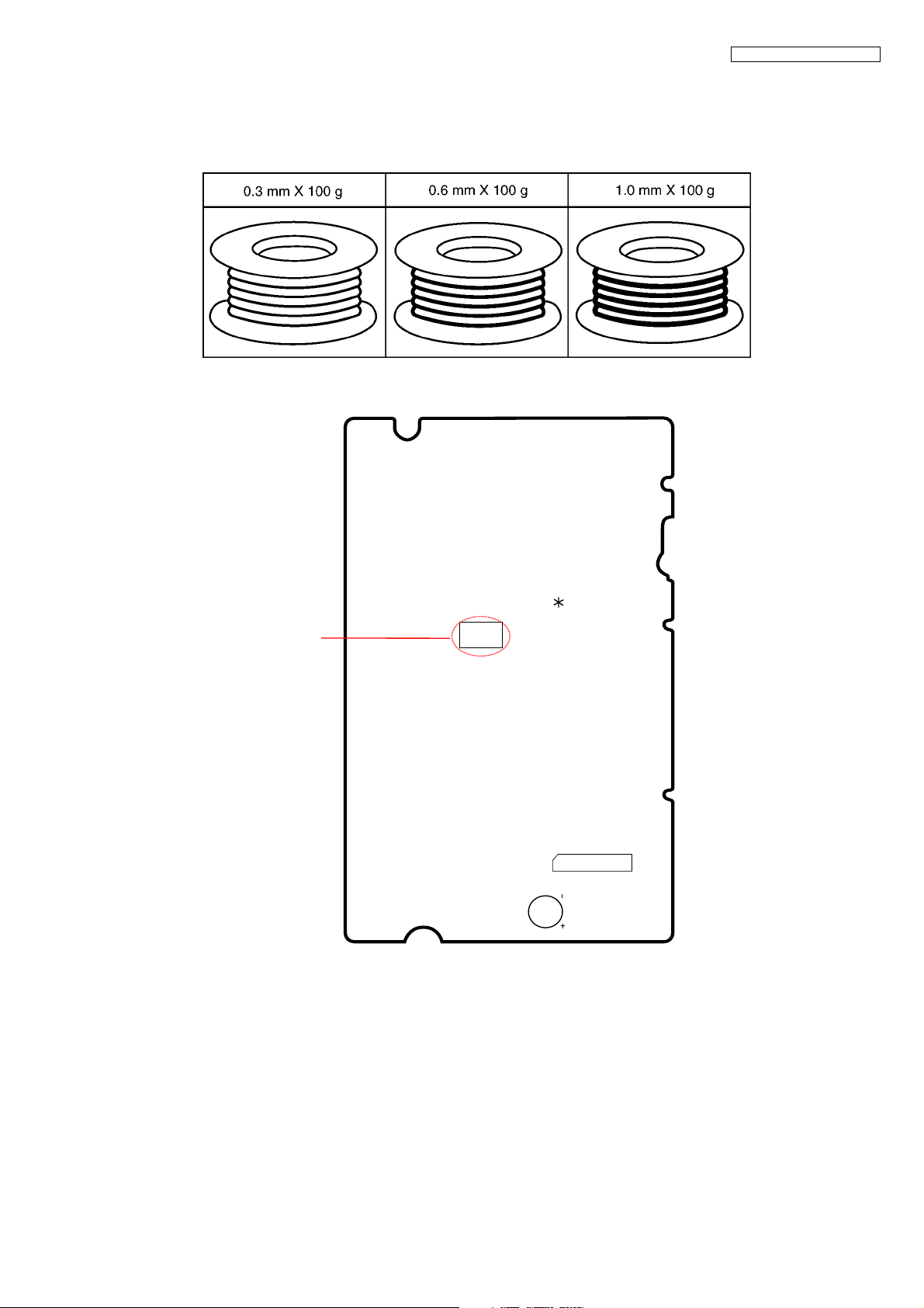
turer’s specific instructions for the melting points of their products and any precautions for using their product with other materials. The following lead free (PbF) solder wire sizes are recommended for service of this product: 0.3 mm, 0.6 mm and 1.0 mm.
2.1.2. How to recognize that Pb Free solder is used
(Example: Operation P.C.B.)
Marked
(Component View)
Note:
The location of the “PbF” mark is subject to change without notice.
PQUP11371Z
PbF
17
18
MIC
CN801
1
2
A
5
KX-TS2570UAB/KX-TS2570UAW
3 Specifications
6

4 Technical Descriptions
4.1. Block Diagram (Base Unit)
T
R
KX-TS2570UAB/KX-TS2570UAW
R1
IC
RINGER
PC1
Ringer indication LED
LED 804 (1AP - SUB)
IC1 D4, D6
D7, D9
Line
Q103, Q104
Q108
Sidetone
Handset
ON/OFF
Bridge
Amp
Sending
V
D304
6.5V
DC Power
IC303, Q301
4.0V
4.0V
Regulator
Reg.
IC304
3.2V
Regulator
IC305
IC903
Power Down
Detection
Reset IC
Q701 Q702
1.8V
D306
Reg.
Q401 D8, D10
KX-TS2570 BLOCK DIAGRAM
T1 D3, D5 C1
Handset / Headset
Speaker
2AP
MIC
SP
Headset
Detection
Q402
IC904
IC902
Amp
SP-Phone
MIC
LSR +
MIC -
Switch
Keyboard
LSR -
MIC +
LINE IN -
HeadsetDET
LINE OUT
FLASH
MEMORY
LCD
RSTn
VDDIO
VBAT2
VDD, AVD
IC901
DSP MICON
NS BBIC
BELL
ACFL
CIDIN+
CIDIN -
JOHN SMITH
1234567890
7
KX-TS2570UAB/KX-TS2570UAW
4.2. Circuit Operation (Base Unit)
4.2.1. Outline
The unit consists of the following ICs as shown in the BLOCK DIAGRAM
• BBIC (Base Band IC): IC901
- Handling all the audio, signal and data processing needed
- ADPCM codec filter for speech encoding and speech decoding (DSP section)
- Echo-cancellation and Echo-suppression (DSP section)
- Any tones (tone, sidetone, ringing tone, etc.) genereation (DSP section)
- DTMF receiver (DSP section)
- ADC, DAC, timer and power control circuitry
- All interfaces (eg: LCD, LED, Analog Front End, etc.)
• FLASH MEMORY : IC902
- Voice Prompt (TAM) Download Area
- Program D/L Area
• RINGER IC : IC1
- Bell signal generator (for bell detection purpose)
• SP AMP : IC904
- Low voltage audio power amplifier
• Additionally,
- Power Supply Circuit (+4.0V, +4.0V, +3.2V, +1.8V output)
- Telephone Line Interface Circuit
- Bell Detection Circuit
- SP-Phone Circuit
- Handset Circuit
-TAM Circuit
4.2.2. Power Supply Circuit
The power is supplied to the BBIC, Flash ROM, SP AMP, Logic IC, LCD, LED from AC adaptor (6.5V)
as below :
• BBIC (IC901) : CN301 (+6.5V) -> D304 -> IC304 -> Q702 -> IC901 (3.2V)
• BBIC (IC901) : CN301 -> D304 ->IC304 -> D701 -> Q701 -> IC901 (1.8V)
• Flash Memory (IC902) : CN301(+6.5V) -> D304 -> IC304 -> Q702 -> IC902
• Logic IC (IC905) : CN301(+6.5V) -> D304 -> IC304 -> Q702 -> IC904
• SP AMP (IC904) : CN301(+6.5V) -> IC305 -> IC904
• LCD (LCD) : CN301(+6.5V) -> D304 -> IC304 -> Q702 -> L302 -> LCD
• LED (LED801, LED802) : CN301(+6.5V) -> IC305 -> L301 -> CN403 -> CN801 -> LED
8
KX-TS2570UAB/KX-TS2570UAW
4.2.3. Telephone Line Interface
• Bell Signal Detection
• Caller ID Detection
• ON/OFF hook Circuit
•Audio Circuit
4.2.3.1. Bell Detection Circuit
When the bell signal is input from LINE to T/R (when the telephone rings), BBIC detects bell signal via following path :
T -> D3 -> IC1(1) -> IC1(8) -> C4 -> R6 -> PC1(1) -> PC1(4) -> IC901(63)
R -> R1 -> LED804 -> D4 -> IC1(1) -> IC1(8) -> C4 -> R6 -> PC1(1) -> PC1(4) -> IC901(63)
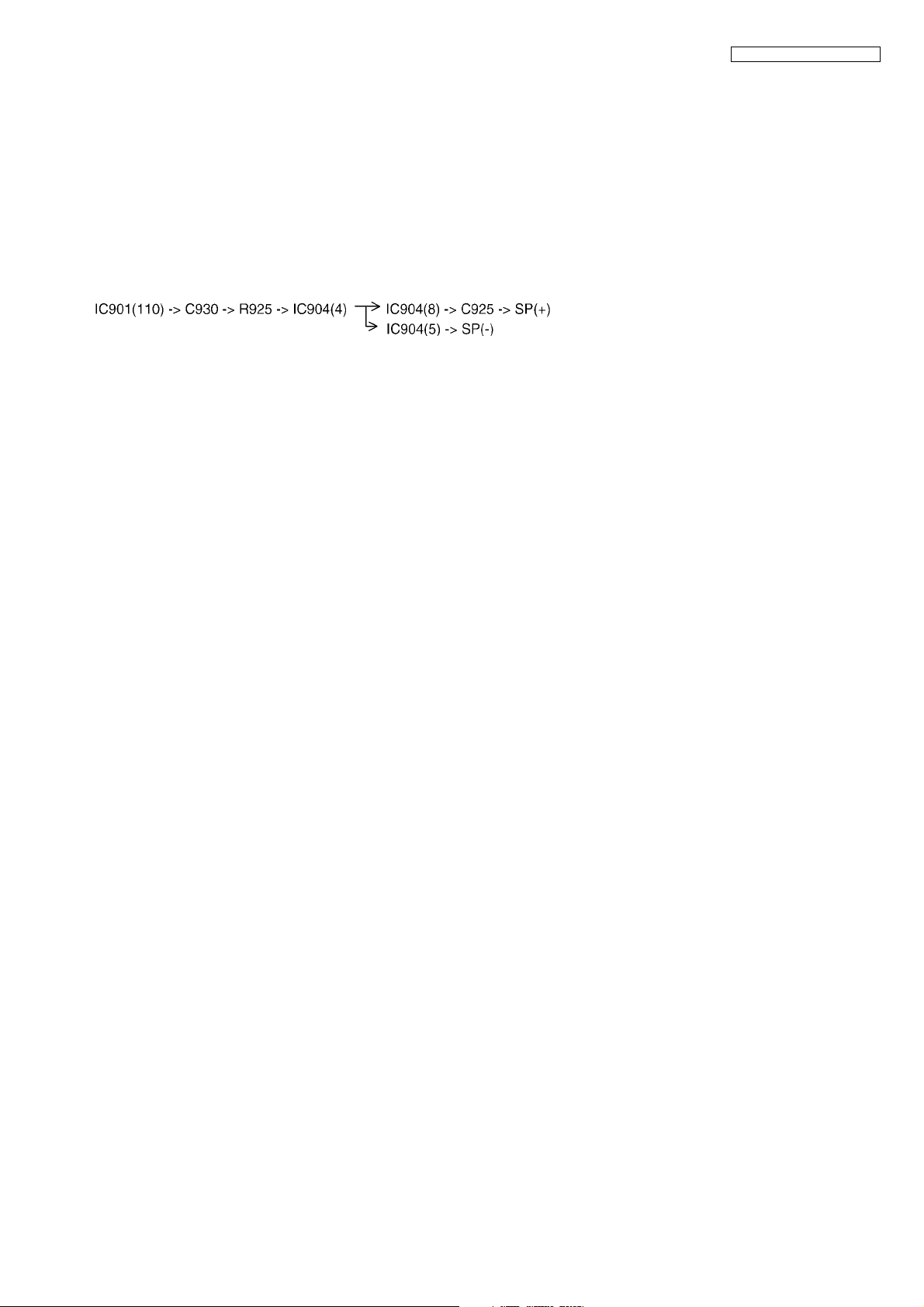
After bell signal detected at IC901(63), the bell ringing signal is output at the speaker via the following path :
4.2.3.2. Caller ID Detection Circuit
Normally, FSK caller ID data is followed after the 1st bell signal.
When the bell signal is detected by BBIC, Caller ID signal is sent through the circuit via
following path :
T -> C501 -> R503 -> R905 -> IC901(107)
R -> C502 -> R504 -> R908 -> IC901(112)
4.2.3.3. On/Off Hook Circuit
In standby mode, SW101 is open and Q104 is OFF. Consequently Q103 is open and cut the DC loop current and voice signal.
This is an on-hook condition.
When handset is picked up or SP-Phone key is pressed, Q104 turns on and then Q103 turns on, thus providing an off-hook condition. A DC loop is made and current flows through the circuit via following path :
T -> D7 -> Q103 -> Q108 -> R124 -> D106 -> D10 -> R
Pulse signal is generated by repeated switches between high (3.2V) and low (0V) logic output from IC901(79), switching the line
loop on and off.
4.2.3.4. Handset Circuit
* Refer to Signal Route
4.2.3.5. Speakerphone Circuit
* Refer to Signal Route
9
KX-TS2570UAB/KX-TS2570UAW
4.3. Ringer IC
10

4.4. Module Block Diagram
4.4.1. LCD Module Block
4.4.2. Connector Pin Assignment
Pin no. Signal Function Enable
1 VDD +3V Power Supply —
2 VSS 0V Power Supply —
3 DB4 Data Bus Line H/L
4 DB5 Data Bus Line H/L
5 DB6 Data Bus Line H/L
6 DB7 Data Bus Line H/L
7 R/W Read / Write H/L
8 E Enable Signal H
9 D/C Data / Command Control H/L
10 CS Chip Signal L
11 RES Reset Signal Input L
KX-TS2570UAB/KX-TS2570UAW
11

KX-TS2570UAB/KX-TS2570UAW
4.5. Signal Route
12

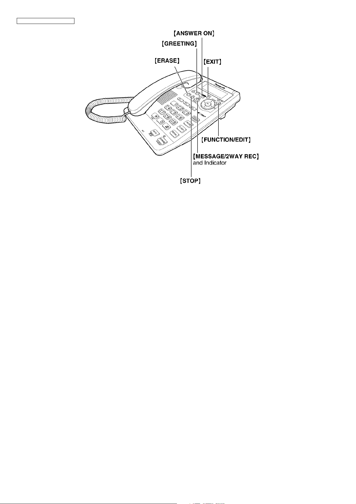
5 Location of Controls and Components
5.1. Controls
KX-TS2570UAB/KX-TS2570UAW
13
KX-TS2570UAB/KX-TS2570UAW
14
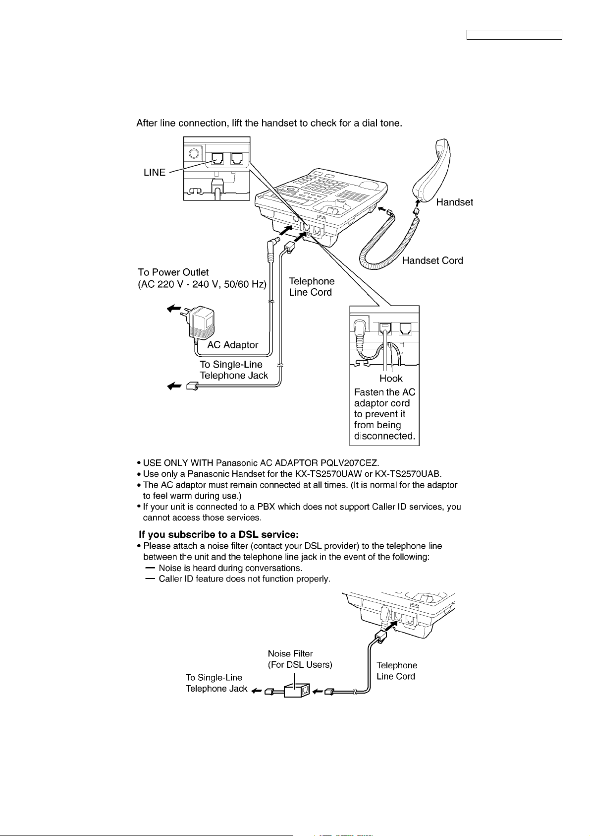
6 Installation Instructions
6.1. Connections
6.1.1. Connecting the Handset/AC Adaptor/Telephone Line Cord
KX-TS2570UAB/KX-TS2570UAW
15

KX-TS2570UAB/KX-TS2570UAW
6.1.2. Connecting a Communication Device
16

7 Operation Instructions
7.1. Dial Lock
7.1.1. To Set the Dial Lock
KX-TS2570UAB/KX-TS2570UAW
7.1.2. To Cancel the Dial Lock
Follow above steps 1 through 3. In step 3, “ “will disappear.
For Service Hint:
(*1): If the current password is forgotten, enter “726276642” at the change password menu and you will be able to change the
password. After you enter a new password, you will be able to cancel the dial lock.
17

KX-TS2570UAB/KX-TS2570UAW
7.2. Troubleshooting
18

KX-TS2570UAB/KX-TS2570UAW
19

KX-TS2570UAB/KX-TS2570UAW
8 Service Mode
8.1. How to Clear User Setting
The unit is reset to the factory settings by this operation (erase recorded Voice messages, stored Phone numbers, Caller list and
etc.).
Note:
This operation should not be performed for a usual repair.
20

9 Troubleshooting Guide
9.1. Troubleshooting Guide
KX-TS2570UAB/KX-TS2570UAW
Cross Reference:
Check Power (P.22)
Check Bell Detection (P.22)
Check Playback (P.23)
Check Record OGM/IGM (P.23)
Check SP-phone Voice Transmission (P.24)
Check SP-phone Voice Reception (P.24)
Check Handset Voice Transmission (P.25)
Check Handset Voice Reception (P.25)
Check Pulse Dial (P.26)
Check DTMF Dial (P.26)
Check Caller ID Detection (P.27)
21

KX-TS2570UAB/KX-TS2570UAW
9.1.1. Check Power
Cross Reference:
Power Supply Circuit (P.8)
9.1.2. Check Bell Detection
Note:
BBIC is IC901.
(*1) Refer to “Specifications” (P.6) for part number and
supply voltage of AC adaptor.
Note:
BBIC is IC901.
22

9.1.3. Check Playback
KX-TS2570UAB/KX-TS2570UAW
Cross Reference:
Power Supply Circuit (P.8)
9.1.4. Check Record OGM/IGM
Note:
BBIC is IC901.
Flash Memory is IC902.
Cross Reference:
Signal Route (P.12)
Bell Detection Circuit (P.9)
On/Off Hook Circuit (P.9)
Note:
BBIC is IC901.
Flash Memory is IC902
23

KX-TS2570UAB/KX-TS2570UAW
9.1.5. Check SP-phone Voice Transmission
Cross Reference:
Signal Route (P.12)
On/Off Hook Circuit (P.9)
9.1.6. Check SP-phone Voice Reception
Note:
BBIC is IC901.
Cross Reference:
On/Off Hook Circuit (P.9)
Signal Route (P.12)
Note:
BBIC is IC901.
24

9.1.7. Check Handset Voice Transmission
KX-TS2570UAB/KX-TS2570UAW
Cross Reference:
Signal Route (P.12)
On/Off Hook Circuit (P.9)
9.1.8. Check Handset Voice Reception
Cross Reference:
On/Off Hook Circuit (P.9)
Signal Route (P.12)
Note:
BBIC is IC901.
Note:
BBIC is IC901.
25

KX-TS2570UAB/KX-TS2570UAW
9.1.9. Check Pulse Dial
Note:
BBIC is IC901.
9.1.10. Check DTMF Dial
Cross Reference:
Signal Route (P.12)
26

9.1.11. Check Caller ID Detection
KX-TS2570UAB/KX-TS2570UAW
Cross Reference:
Bell Detection Circuit (P.9)
Caller ID Detection Circuit (P.9)
27

KX-TS2570UAB/KX-TS2570UAW
9.2. How to Replace the Flat Package IC
Even if you do not have the special tools (for example, a spot heater) to remove the Flat IC, with some solder (large amount), a
soldering iron and a cutter knife, you can easily remove the ICs that have more than 100 pins.
9.2.1. Preparation
• PbF (: Pb free) Solder
• Soldering Iron
Tip Temperature of 700°F ± 20°F (370°C ± 10°C)
Note: We recommend a 30 to 40 Watt soldering iron. An expert may be able to use a 60 to 80 Watt iron where someone with
less experience could overheat and damage the PCB foil.
•Flux
Recommended Flux: Specific Gravity → 0.82.
Type → RMA (lower residue, non-cleaning type)
Note: See About Lead Free Solder (Pbf: Pb free) (P.4).
9.2.2. How to Remove the IC
1. Put plenty of solder on the IC pins so that the pins can be completely covered.
Note:
If the IC pins are not soldered enough, you may give pressure to the P.C. board when cutting the pins with a cutter.
2. Make a few cuts into the joint (between the IC and its pins) first and then cut off the pins thoroughly.
3. While the solder melts, remove it together with the IC pins.
When you attach a new IC to the board, remove all solder left on the board with some tools like a soldering wire. If some solder is
left at the joint on the board, the new IC will not be attached properly.
28

9.2.3. How to Install the IC
1. Temporarily fix the FLAT PACKAGE IC, soldering the two marked pins.
*Check the accuracy of the IC setting with the corresponding soldering foil.
2. Apply flux to all pins of the FLAT PACKAGE IC.
3. Solder the pins, sliding the soldering iron in the direction of the arrow.
KX-TS2570UAB/KX-TS2570UAW
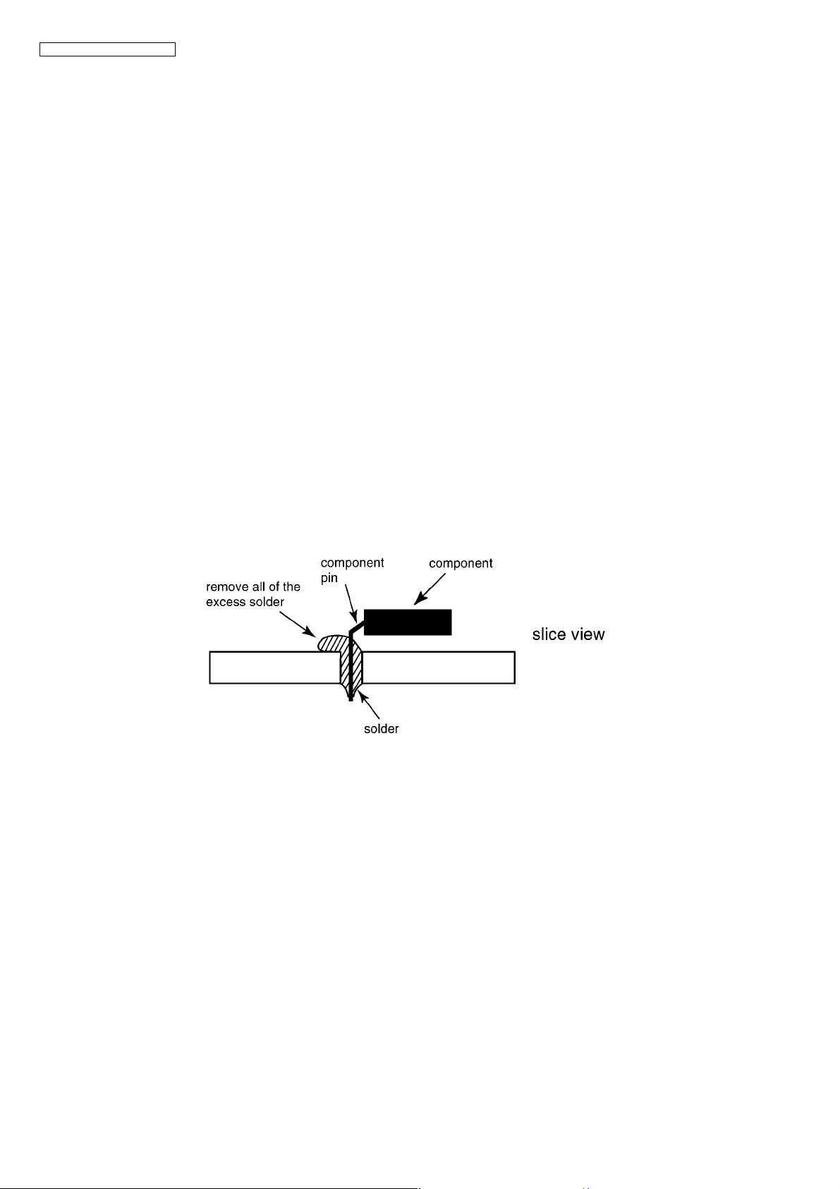
9.2.4. How to Remove a Solder Bridge
1. Lightly resolder the bridged portion.
2. Remove the remaining solder along the pins using a soldering iron as shown in the figure below.
29

KX-TS2570UAB/KX-TS2570UAW
10 Disassembly and Assembly Instructions
30

KX-TS2570UAB/KX-TS2570UAW
11 Schematic Diagram
11.1. For Schematic Diagram
1. SW1: Hook switch.
2. DC voltage measurements are taken with electronic voltmeter from negative voltage line.
3. (Add 40 mA to telephone line from the loop simulator.)
4. Off-hook condition
5. No Mack: Handset Mode
6. This schematic diagram may be modified at any time with the development of new technology.
7. The shades area on this schematic diagram incorporates special features important for protection from fire and elec-
trical shock hazards.
8. When servicing, it is essential that only manufacture's specified parts be used for the critical components in the
shaded areas of the schematic.
31

KX-TS2570UAB/KX-TS2570UAW
11.2. Schematic Diagram (Main)
CN403
MSG_LED
SP_LED
VDD
STB5
STB4
STB3
STB2
STB1
STB0
KIN5
KIN4
KIN3
KIN2
KIN1
KIN0
NC
MIC
GND
R933 1K
1
R935 1K
2
3
4
5
6
7
8
9
RA3
10
220
1
8
11
2
7
3
6
12
45
13
220R927
14
220R926
15
TP601
16
17
TP602
18
SP-Phone TX
- Audio
LCD
1
Vcc
2
GND
3
D4
4
D5
5
D6
6
D7
7
R/W
8
E
9
D/C
10
CS
11
RES
AD17
AD16
AD15
AD14
AD13
AD12
AD11
AD10
AD9
AD21
+3.2V
AD19
R903
AD18
100
AD8
AD7
AD6
AD5
AD4
AD3
AD2
AD1
L301
L302
L321
L322
L323
L324
L325
L326
L327
L328
L329
(1)
(2)
(3)
(4)
(5)
(6)
(7)
(8)
D907
D908
D909
D910
D911
D912
C955
C937
Z0.1
Q901
6.3V22
R932
R934
100
2.2K
Q902
IC905
1
CLR
2
1Q
3
1D
4
2D
5
2Q
6
3Q
7
3D
8
4D
9
4Q
10
GND11CLK
+3.2V
VCC
3.2V
DC
L318
DAB0
DAB1
K0.1C956
20
19
8Q
18
DAB7
8D
17
DAB6
7D
16
7Q
15
6Q
14
DAB5
6D
13
DAB4
5D
12
5Q
DAB3
DAB2
C930
K0.015
C927
Z1.0
C928
Z1.0
R925
39K
D920
IC904
1
CD
2
FC2
3
FC1
4
C929 K220P
C925
8
VO2
6.3V220
7
GND
6
VCC
5
VO1
C926
120KR924
K0.1
4.0V
DC
TP603
TP604
3.2V
DC
R704
5.6K
Q702
C703
16V10
C704
+3.2V
R702
R703
5.6K
C707
2.2K
D701
C706
16V1000
K0.1
Q701
15K
R701
C702
16V10
+1.8V
C705
C7
16V10
SPH+
SP
SPH-
SP-Phone RX
- Audio
- Bell signal
- Tone
1.8V
DC
RX (OFF Hook)
- Audio
T1
5
1
4
2
3
R8
1K
- Call waiting
SW101
C943
Z0.1
C958
SW101
(9)
(10)
(11)
(12)
(13)
(14)
(15)
(16)
(17)
(18)
(19)
(20)
(21)
(22)
(23)
(24)
(25)
(26)
(27)
(28)
+3.2V
R992
100
L311
Z0.1C924
L313
23 AVS
79
PULSE
24 AVD
78
RA5
220
VDDIO
25 RSSI
77
VDD
26 RDI
L306
76
VSS
27 CMPREF
L316
C941 Z0.1+1.8V
C959 K1000P
C940 Z0.1
DAB11
DAB3
DAB10
DAB2
DAB9
123
45
678
73
74
75
72
DAB3
DAB271DAB970DAB169DAB868DAB067SDA2
DAB10
DAB11
31 AD17
28 TDO
29 AD15
30 AD16
32 AD18
AD15
AD16
AD17
AD18
DAB1
45
AD19
DAB8
678
AD20
34
DAB0
123
RA4
220
66
65
BE0n
BE1n
BELL
NEW_MSG
ROW5
HSIN
IOCS
HOOKDET
ACFL
VDDIO
ROW4
ROW3
ROW2
ROW1
ROW0
SCLK
MI/READY
HeadsetDET
EXHOOOKDET
AD2336AD2235AD2133AD19
38LE37
AD21
64
63
ROW5
62
61
60
CE
59
L317
58
57
56
VSS
55
ROW4
54
ROW3
53
ROW2
52
ROW1
51
50
49
JTIO
48
URX
47
UTX
46
45
44
WE
43
OE
42
41
40
SK
39
SO
ROW0
R133
K1000P
0R914
0R915
1M
L315
R997 10K R998 10K
C949
NC
103
LD01_Sence
104
LD01_CTRL
105
LD02_CTRL
106 VBAT2
107 CIDIN+
108
AVS2
109
AVD2
110
LSR+/REF
111
LSR-/REF
112
CIDIN-
113
CIDOUT
114
MIC-
115
VREF-
116
VBUF
117
AGND
118
MIC+
119
VREF+
120
RSTn
121
AD0/EXT_MEMORY
122
AD1
123
AD2
124
AD3
125
AD4
126
AD5
127
AD6
128
AD7
C957
+1.8V
K1000P
102
LINE_IN-
1 VDDIO
C947 J10P
L312
100
101
LINE_IN+
LINEOUT
2 VSS
3AD8
AD8
AD9
97
98
99
LINEREF
RINGING
P2[6]/stop_charge
4AD9
5AD10
6AD11
AD10
AD11
AD12
DAB15
DAB7
45
RA7
220
678
91
92
93TM94
95
96
RLY
DAB7
DAB15
P1[6]/PON/INT6n
P1[7]/CHARGE/INT7n
7AD12
8AD13
9AD14
10 SPLED
11 D/C
12 D7
AD13
AD14
L305
DAB14
90
DAB14
13 D6
DAB6
89
DAB13
123
DAB6
14 D5
88
DAB13
15 D4
C946 K0.1 R991 100
R902
100K
C906
NC
K0.1
C945
R990
K0.022
R989
100K
C914
K0.047
1K
Z0.1
R909
R952
2.2K
R951
2.2K
TP905
D902
R905
100K
C907
C944
K220P
100
D901
K220P
IC903
3.2V
C908
DC
IC902
16MB
1
A16
A15
2
BYTE
A14
3
VSS
A13
4
DQ15
A12
5
DQ7
A11
6
DQ14
A10
7
DQ6
A9
8
DQ13
A8
9
DQ5
A19
10
DQ12
NC
11
DQ4
WE
12
VCC
RESET
13
DQ11
NC
14
DQ3
WP
15
DQ10
RY
16
DQ2
A18
17
DQ9
A17
18
DQ1
A7
19
DQ8
A6
20
DQ0
A5
21
OE
A4
22
VSS
A3
23
CE
A2
24
A1
A0
R904
+3.2V
48
47
46
45
DAB15
44
DAB7
43
DAB14
42
DAB6
DAB13
DAB5
DAB12
DAB4
DAB11
DAB3
DAB10
DAB2
DAB9
DAB1
DAB8
DAB0
+3.2V
L304
+3.2V
R988
41
40
39
38
37
36
35
34
33
32
31
30
29
28
27
26
25
C938
R908
C904
GND
+1.8V
100
C952
K3300P
C915
VCCVOUT
NC
2.7V
J10P
C950
J10P
C903
K3300P
+3.2V
TP902
C939 Z0.1
TP903
K0.056
C901
TP904
Z0.22
1KR906
C942
NC
AD1
AD2
AD3
AD4
AD5
AD6
AD7
+3.2V
C909 Z0.01
DAB5
45
87
DAB5
DAB12
678
16 VDD
DAB4
86
DAB12
17 VSS
123
RA6
220
83CS84
85
RES
DAB4
IC901
18 RFCLK
19 VDDRF
20 VSSRF
100
R993
L314
80
81E82
R/W
AGC
3.2V DC
1.8V DC
0V
21 XTAL
22 CAP
NC: No Components
32
Z0.1C948
R913
10.368M
X900
C910
C911
J18P
J15P
C913
(29)
(30)
Z0.1

KX-TS2570UAB/KX-TS2570UAW
(10)
(11)
(12)
(13)
(14)
(15)
(16)
(17)
(18)
R11
R109
C1
D3
250V1.0
D4
D5
D6
CP1
680K
R116 47K
C110
R117
6.8K
Q109
D2
LED804
D101
Loop
C105
current
16V220
D103
K1.0
4.7K
R118
D501 NC
C312
C306
6.3V22 C305
4
NC
1
23
PC3
NC
18VD104
100K
R110
C104 K4700P
NC
C506 NC
6.3V330
C315
R106
47K
C505 NC
R305
D306
R303 12
Z0.1
C112 NC
Q107
R107
D502 NC
0
3.3K
Q110
R122
56K
C308
6.3V330 C307
CP2
LED ON SUB PCB
Q103
Q104
R103
C108
K0.01
4.0V
DC
Z0.1
C313
6.3V22
4.0V
DC
Z0.1
R420 47K
R108
1M
C503
K1000P
C504
K1000P
5
4
5
4
10V DC (OFF Hook)
0V DC (ON Hook)
R1
4.7K
100K
10M
R101
R113
SW101
4.7K
R105
470K
R112
2.7MR104
NC
1MR503
180KR501
180KR502
1MR504
2.2MR102
C103 Z0.01
Q101
Q102
RX (ON Hook)
- Caller ID
IC305
1
VIN
VOUT
2
NC
4.0V
IC304
VOUT
NC
4.0V
VSS
NC
VIN
VSS
NC
C310
3
C311
Z0.1
1
2
3
C309
C304Z0.1
R114
R115
K1500P/500VC501
K1500P/500VC502
C303
+3.2V
K0.1
NC
4.7K
10V100
D304
10V100
R307
C102
K680P
100K
C101
K680P
D10
D7
D8
D9
R301
R302
Q301
Line Voltage
48V DC (ON Hook)
10V DC (OFF Hook)
TP102
L3
SA101
SA102
L4
POS101
JP102
TP101
DC1
C302NC
VCC
NC
5.0V
C301 K0.01
VOUT
33uH
33uH
IC303
22K
GND
NC
L1
L2
JJ101
1
2
JJ102
2
1
DATA
CN301
1
2
TIP
RING
TEL
TIP
RING
6.5V
GND
DC2
(1)
(2)
Q1
(3)
Q2
(4)
(5)
(6)
(7)
(8)
(9)
R936
8.2K
8.2K
C953
K1500P
R910
C905
1.5M
K0.01
R5
R937
PC2
PC1
R6
1
23
0
4
C6
K0.1
47K
1234
C5
R7 10K
C114
C951
C954
K1500P
R304100K
C4
50V1
120K
K8200P
R131
10K
R130
16V10
C120
J10P
K0.033
R4
1K
8
OUT
7
HFI
6
HFO
5
VSS
C113
K0.022
R123
33
1K
R125
K0.1
C118
TX
- Audio
- Tone
6.3V330 C316
IC1
R124
C10710V330
C317
VDD
CONT
LFI
LFO
C116
NC
C117
K0.01
15(1/2W)
D106
Z0.1
1
R2
2
39K
3
R3
4
330K
Q108
6.2V
R306 12
C3
C111
NC
R9
30V
D1
50V0.22
R121
15K
D102
R119
C2
2.2K
R120
C106
Q3
50V4.7
C115
0
16V10
R111
D105
JP101
R10
NC
K0.015
Q106
0
Q105
10K
R308
(19)
(20)
(21)
(22)
(23)
(24)
(25)
(26)
(27)
(28)
(29)
(30)
TP901
1K
R987
UTXGND JTIOURX
R986
1K
R985
100
D905
For ROM-WRITE
R994
R995
R996
Handset/Headset TX
- Audio
10K
10K
1K
4.7V
4.7V
D904
D903
Handset/Headset RX
- Audio
- Tone
4.7V
C417
K0.01
C423
Q401
K390P
R414
R415
2.2K
C421
J100P
390
R413
K1000P
C420
3.3M
C416
K0.1
R422
Handset
100K
R419
TP402
L303
TP401
CN401
1 MIC(+)
R430
C419
TP403
0
K1000P
2
3
4
5
1
L307
2 MIC(-)
L308
3 SP(+)
L309
4 SP(-)
L310
CN402
Headset Jack
22K
0
3.3K
R410
C413
R416
NC
K0.01
C422
C414
C418 NC
R411
10K
K2200P
C415
K0.1
R412
68K
33
NC
Q402
R417
470K
R418
C428
10V22
Headset
NC: No Components
KX-TS2570UA SCHEMATIC DIAGRAM (MAIN)
33

KX-TS2570UAB/KX-TS2570UAW
11.3. Schematic Diagram (Operation)
MUTE
FUNCTION
EXIT
ANSWER ON
HOLD
Greeting
CN801
1MSG_LED
2SP_LED
3VDD
4STB5
5STB4
6STB3
7STB2
8STB1
9STB0
10KIN5
11KIN4
12KIN3
13KIN2
14KIN1
15KIN0
16NC
17MIC
18GND
ANS_LED
SP_LED
VCC
MICP
MICM
LED802
MSG_LED
LED801
SP_LED
STB5
STB4
STB3
STB2
STB1
STB0
KIN5
KIN4
KIN3
KIN2
KIN1
KIN0
MIC
KIN0
KIN1
KIN2
KIN3
KIN4
KIN5
SP-PHONE
*
7
4
1
STB0
STB1
M1
M2
0
8
5
2
#
9
6
3
STB2
M3
REDIAL
PAUSE
FLASH
KEYLOCK
STB3
OK
NAVI_RIGHT
NAVI_LEFT
VOL_UP
VOL_DOWN
STB4
Erase
STOP
MESSAGE
NC: No Components
KX-TS620 SCHEMATIC DIAGRAM (OPERATION)
34

12 Printed Circuit Board
25
C914
L304
D2
RED WHITE
D5 D3 D4 D6
D1
D306
PC1
T1
D102
D901
D902
D904
D905
D903
Q1
Q301
LCD
PbF
Q3
Q2
Q106
Q104
Q109
Q103
Q108
Q702
Q701
RING
CP2 CP1
A
WHITE
RED
GREEN YELLOW GREEN
JJ101
JJ102
YELLOW
POS101
TIP
RING TIP
LED804
R307
R11
R10
R302
R301
R5
R502
R3
R9
R503
R2
R6
R4
R7
R304
R998
R997
4
1
R992
R951
R303
5
13
4
R952
R906
R904
R913
R993
R915
RA5
RA4
RA6
RA3
10
1
5
8
1
20
11
RA7
R985
R996
R914
C309
C301
C505
C6
C1
C924
L302
C3
C2
C5
C4
C938
C111
C705
C317
R306
D701
R701
C306
C304
C315
C942
C904
IC901
IC1
IC303
IC304
KX-TS620
C910
C911
C913
C948
C958
C943
C959
C941
C930
C905
R910
C118
C114
34
21
L3
L4
L329
L325
L321
L327
L324
L323
L322
L326
L328
L311
L313
L312
L314
L305
1
128
103
102
GND UTX URX
PQUP11370Y
PQUP11370Z
L317
L315
D7
PC2
PC3
CP2
CN301
JP102
PbF
CP1
D9
D8
D10
D304
D502
D501
D106
C303
C305
C316
C707
R1
R988
R124
C107
R111
R118
R117
R8
C302
8
1
4
5
JP101
R909
R902
R991
R704
R703
R702
R905
C950
R908
R501
R504
X900
R903
R986
R995
R133
R987
R994
C106
D101
C120
C102
R116
R107
R418
R924
R416
R413
R417
R990
R410
R412
R414
R927
R926
R415
R411
R108
CBE
CBE
CBE
CBECBE
C
L303
L308 L307 R430
CN402
CN401
BE
C101
C502
C501
C7
C949
C908
C110
C907
C947
C946
C906
C704
C703
C901
C903
C915
C504
C506
C503
C952
C939
C909
C957
C706
C702
C307
C940
C954
C956
C945
C953
R989
R936
R937
C944
C951
L2
L1
Q105
R131
R130
R110
R109
R119
R120
R121
R123
R125
C104
C113
C117
C116
C115
SA101
SA102
L318
L316
L306
48
17
18
39
64
65
38
1
24
D903
D920
D104
D105
Q902
Q901
Q401
Q402
Q102
SW101
Q107
R933
R935
R932
R934
2
R925
IC305
IC905
IC903
IC902
IC904
R419
R422
R420
R308
R305
R106
R115
R122
R112
R103
R101
R114
R102
C103
R105
R104
R113
CN403
C925
A
C937
C422
C420
C421
C423
C417
3
45
1
C308
C313
C312
C105
C108
C112
L301
L309
BLACK
RED
GREEN
YELLOW
L310
D910
D909
D911
D912
D103
Q101
Q110
C929
C926
D907
C955
C413
C416
C415
C428
C418
C414
C928
C927
C419
C311
C310
KX-TS2570 CIRCUIT BOARD (MAIN) Component View
12.1. Circuit Board (Main)
12.1.1. Component View
KX-TS2570UAB/KX-TS2570UAW
35

KX-TS2570UAB/KX-TS2570UAW
12.1.2. Flow Solder Side View
A
TP304
PbF
A
WHITE
RED
PbF
PQUP11370Z
DC1
TP102
DC2
TP101
TP301
TP905
TP903
TP902
URXGND
UTX
TP302
TP904
TP901
JTIO
VDD
TP602
KIN2
STB0
STB4
TP601
KIN0
KIN4
STB2
SP_LED
PQUP11370Y
KIN1
KIN5
STB1
STB3
KIN3
STB5
MSG_LED
RED
TP604
SP_PHONE
TP303
SW101_1_1
SW101_1_2
TP402
KX-TS2570 CIRCUIT BOARD (MAIN) Flow Solder Side View
TP401
MIC
WHITE
TP603
TP403
SP
36

12.2. Circuit Board (Operation)
12.2.1. Component View
KX-TS2570UAB/KX-TS2570UAW
PQUP11371Z
PbF
17
18
MIC
KX-TS2570 CIRCUIT BOARD (OPERATION) Component View
CN801
1
2
A
37

KX-TS2570UAB/KX-TS2570UAW
12.2.2. Flow Solder Side View
KEYLOCK
GREETING
ERASE_620
KIN1
KIN5
M1 M2 M3
STOP
STB5
ANS_LED
VCC
STB2
ANS_ON_620
LED802
TS620
MESSAGE
EXIT
ERASE_600
NAVI_LEFT
VOL_UP
OK
VOL_DOWN
PQUP11371Z
123
456
PbF
FUNCTION
NAVI_RIGHT
STB4
STB1
STB3
KIN4
KIN0
HOLD
PAUSE
SP_LED
A
7
CN801
KIN3
STB0
89
SHARP
MUTE
LED801
TS600
TS620
MICM
-
0
KIN2
MICP
FLASH
REDIAL
SP-PHONE
+
KX-TS2570 CIRCUIT BORAD (OPERATION) Flow Solder Side View
38

13 Appendix Information of Schematic Diagram
13.1. CPU Data
PIN I/O Description High High_Z Low
PIN I/O Description High High_Z Low
1 - VDDIO -- -- -2-VSS -- -- -3D.OAD8 -- -- -4D.OAD9 -- -- -5 D.O AD10 -- -- -6 D.O AD11 -- -- -7 D.O AD12 -- -- -8 D.O AD13 -- -- -9 D.O AD14 -- -- --
10 D.O SP_LED ON -- OFF
11 D.O D/C Data -- Command
12 D.O D7 Active -- Active
13 D.O D6 Active -- Active
14 D.O D5 Active -- Active
15 D.O D4 Active -- Active
16 - VDD -- -- -17 - VSS -- -- -18 D.O RFCLK -- -- -19 - VDDRF -- -- -20 - VSSRF -- -- -21 A.I Xtal1 -- -- -22 A.I CAP -- -- -23 - AVS -- -- -24 - AVD -- -- -25 A.I RSSI -- -- -26 A.I RXDA -- -- -27 A.I CMPREF -- -- -28 A.O TDO -- -- -29 D.O AD15 -- -- -30 D.O AD16 -- -- -31 D.O AD17 -- -- -32 D.O AD18 -- -- -33 D.O AD19 -- -- -34 D.O NC -- -- -35 D.O AD21 -- -- -36 D.O NC -- -- -37 D.O NC -- -- -38 D.O LE -- -- -39 D.O SO -- -- -40 D.O SK -- -- -41 A.I EXHOOKDET EX OFF-
HOOK
42 D.I HeadSetDET Headset
On
43 D.O OE -- -- -44 D.O WE -- -- -45 D.I NC -- -- -46 D.O NC -- -- -47 D.O UTX High -- Low
48 D.I URX High -- Low
49 D.I/O JTIO High -- Low
50 D.I ROW0 Normal -- Active
51 D.I ROW1 Normal -- Active
52 D.I ROW2 Normal -- Active
53 D.I ROW3 Normal -- Active
54 D.I ROW4 Normal -- Active
55 - VDDIO -- -- -56 - VSS -- -- -57 D.I ACFL power fail-
ure
58 D.I HOOKDET On-Hook -- Off-Hook
59 D.O IOCS Clock -- Normal
-- EX ONHOOK
-- Headset
OFF
-- Normal
60 D.O ACS0 Normal -- Select
61 D.O HSIN Normal -- CLEAR
62 D.I ROW5 Normal -- Active
63 D.I BELL Normal -- Bell input
64 D.O NC -- -- -65 D.O NC -- -- -66 D.O RLY On -- Off
67 D.I/O NC -- -- -68 D.I/O DAB0 Active -- Active
69 D.I/O DAB8 Active -- Active
70 D.I/O DAB1 Active -- Active
71 D.I/O DAB9 Active -- Active
72 D.I/O DAB2 Active -- Active
73 D.I/O DAB10 Active -- Active
74 D.I/O DAB3 Active -- Active
75 D.I/O DAB11 Active -- Active
76 - VSS -- -- -77 - VDD -- -- -78 - VDDIO -- -- -79 D.O PULSE Break -- Make
80 D.O R/W Read -- Write
81 D.O E Active -- Normal
82 A.I AGC analog
input
83 D.O CS Normal -- Select
84 D.O RES Normal -- Reset
85 D.I/O DAB4 Active -- Active
86 D.I/O DAB12 Active -- Active
87 D.I/O DAB5 Active -- Active
88 D.I/O DAB13 Active -- Active
89 D.I/O DAB6 Active -- Active
90 D.I/O DAB14 Active -- Active
91 D.I/O DAB7 Active -- Active
92 D.I/O DAB15 Active -- Active
93 D.I TM -- -- -94 D.O NEWMSG_LED ON -- OFF
95 A.I NC -- -- -96 D.I/O NC -- -- -97 D.O NC -- -- -98 A.I RINGING -- -- -99 A.O LINEREF -- -- --
100 A.O LINEOUT -- -- -101 A.I LINE_IN+ -- -- -102 A.I LINE_IN- -- -- -103 A.I LDO1_Senes -- -- -104 A.O LDO1_CTRL -- -- -105 A.O LDO2_CTRL -- -- -106 A.I VBAT2 -- -- -107 A.I CIDIN+ -- -- -108 - AVS2 -- -- -109 - AVD2 -- -- -110 A.O LSR+/REF -- -- -111 A.O LSR-/REF -- -- -112 A.I CIDIN- -- -- -113 A.O CIDOUT -- -- -114 A.I MIC- -- -- -115 A. O VREF - -- -- -116 A.O VBUF -- -- -117 A.O AGND -- -- -118 A.I MIC+ -- -- -119 A.O NC -- -- -120 A.I RSTn -- -- -121 D.I EXT_MEMORY -- -- --
KX-TS2570UAB/KX-TS2570UAW
-- --
39

KX-TS2570UAB/KX-TS2570UAW
PIN I/O Description High High_Z Low
122 D.O AD1 -- -- -123 D.O AD2 -- -- -124 D.O AD3 -- -- -125 D.O AD4 -- -- -126 D.O AD5 -- -- -127 D.O AD6 -- -- -128 D.O AD7 -- -- --
Note:
Data in the blank columns are omitted because of the Analog I/O.
40

13.2. Terminal Guide of the Ics, Transistor and Diodes
KX-TS2570UAB/KX-TS2570UAW
41

KX-TS2570UAB/KX-TS2570UAW
14 Exploded View and Replacement Parts List
14.1. Cabinet and Electric Parts
42

14.2. Accessories and Packing Materials
KX-TS2570UAB/KX-TS2570UAW
43

KX-TS2570UAB/KX-TS2570UAW
14.3. Replacement Part List
1. RTL (Retention Time Limited)
Note:
The marking (RTL) indicates that the Retention Time
is limited for this item.
After the discontinuation of this assembly in production, the item will continue to be available for a specific
period of time. The retention period of availability is
dependant on the type of assembly, and in accordance with the laws governing part and product retention. After the end of this period, the assembly will no
longer be available.
2. Important safety notice
Components identified by the mark indicates special
characteristics important for safety. When replacing any
of these components, only use specified manufacture’s
parts.
3. The S mark means the part is one of some identical parts.
For that reason, it may be different from the installed part.
4. ISO code (Example: ABS-94HB) of the remarks column
shows quality of the material and a flame resisting grade
about plastics.
5. RESISTORS & CAPACITORS
Unless otherwise specified;
All resistors are in ohms (Ω) K=1000Ω, M=1000kΩ
All capacitors are in MICRO FARADS (µF)P=µµF
*Type & Wattage of Resistor
Ref.
No.
7 PQSX10309Y KEYBOARD SWITCH, 13 KEY (for
7 PQSX10309Z KEYBOARD SWITCH, 13 KEY (for
8 PQBH10043Z2 BUTTON, HOOK (for KX-
8 PQBH10043Z1 BUTTON, HOOK (for KX-
9 PQAS57P03Z SPEAKER
10 PQBC10455Z3 BUTTON, MUTE (for KX-
10 PQBC10455Z1 BUTTON, MUTE (for KX-
11 PQBC10455Y4 BUTTON, SP PHONE (for KX-
11 PQBC10455Y2 BUTTON, SP PHONE (for KX-
12 PQBX10389Q2 BUTTON, DIAL KEY (for KX-
12 PQBX10389Q1 BUTTON, DIAL KEY (for KX-
13 PQSX10308Y KEYBOARD SWITCH, 21 KEY (for
13 PQSX10308Z KEYBOARD SWITCH, 21 KEY (for
14 PQMG10025Z RUBBER PARTS, MIC
15 PQHG10622Z RUBBER PARTS, SHEET
16 J0KD00000070 FILTER
17 PQKF10696V2 CABINET COVER (for KX-
17 PQKF10696V1 CABINET COVER (for KX-
18 PQHA10018Y RUBBER PARTS, FOOT CUSHION
19 PQKL10072Z2 STAND, WALL MOUNT (for KX-
19 PQKL10072Z1 STAND, WALL MOUNT (for KX-
20 PQHA10025Z RUBBER PARTS, FOOT CUSHION
21 PQGT19251Z NAME PLATE (for KX-TS2570UAB)
21 PQGT19250Z NAME PLATE (for KX-TS2570UAW)
22 PQQT23324Z INDICATIONPLATE-LABEL
Part No. Part Name & Description Remarks
KX-TS2570UAB)
KX-TS2570UAW)
TS2570UAB)
TS2570UAW)
TS2570UAB)
TS2570UAW)
TS2570UAB)
TS2570UAW)
TS2570UAB)
TS2570UAW)
KX-TS2570UAB)
KX-TS2570UAW)
TS2570UAB)
TS2570UAW)
TS2570UAB)
TS2570UAW)
ABS-HB
ABS-HB
ABS-HB
ABS-HB
ABS-HB
ABS-HB
ABS-HB
ABS-HB
PS-HB
PS-HB
PS-HB
PS-HB
14.3.1. Cabinet and Electrical Parts
14.3.1.1. Cabinet and Electrical Parts
Ref.
No.
1 PQGP10298Z1 PANEL, LCD
2 PQHR11185Z OPTIC CONDUCTIVE PARTS, LED
3 PQKM10704M2 CABINET BODY (for KX-
3 PQKM10704M1 CABINET BODY (for KX-
4 PQBC10456Y2 BUTTON, NAVI KEY (for KX-
4 PQBC10456Y1 BUTTON, NAVI KEY (for KX-
5 PQHR11184Z HOLDER, NAVI KEY POM-HB
6 PQBC10454Z2 BUTTON, OK (for KX-TS2570UAB) PS-HB
6 PQBC10454Z1 BUTTON, OK (for KX-TS2570UAW) PS-HB
Part No. Part Name & Description Remarks
LENS
TS2570UAB)
TS2570UAW)
TS2570UAB)
TS2570UAW)
PS-HB
ABS-HB
ABS-HB
PS-HB
PS-HB
14.3.1.2. Main P. C. Board Parts
Ref.
No.
PCB1 PQWP1S2570UA MAIN P.C. BOARD ASS'Y (RTL)
IC1 C1CB00002315 IC
IC303 PQVIPS3450UT IC
IC304 C0CBACC00036 IC
IC305 C0CBACC00036 IC
IC901 C1CB00001879 IC
IC902 PQWITS2570UA IC
IC903 PQVIPS3327UT IC
IC904 C1BB00001024 IC
IC905 PSVISNLV273A IC S
Q1 UN5213 TRANSISTOR(SI) S
Q2 UN5213 TRANSISTOR(SI) S
Q101 2SD1819A TRANSISTOR(SI)
Q102 UN5213 TRANSISTOR(SI) S
Q103 B1ACGP000007 TRANSISTOR(SI)
Q104 PQVT2N6517CA TRANSISTOR(SI) S
Q105 2SD1819A TRANSISTOR(SI)
Q106 2SA933 TRANSISTOR(SI) S
Q107 2SD1819A TRANSISTOR(SI)
Q108 B1AAKD000013 TRANSISTOR(SI)
Q109 B1CEGF000004 TRANSISTOR(SI)
Q301 UN5213 TRANSISTOR(SI) S
Q401 2SD1819A TRANSISTOR(SI)
Q402 2SD1819A TRANSISTOR(SI)
Q701 B1ADGE000004 TRANSISTOR(SI)
Q702 B1ADGE000004 TRANSISTOR(SI)
Q901 UN5213 TRANSISTOR(SI) S
Q902 UN5213 TRANSISTOR(SI) S
Part No. Part Name & Description Remarks
(ICs)
(TRANSISTORS)
44

KX-TS2570UAB/KX-TS2570UAW
Ref.
No.
D1 MA4300 DIODE(SI) S
D2 B0EAAD000001 DIODE(SI)
D3 B0EAAD000001 DIODE(SI)
D4 B0EAAD000001 DIODE(SI)
D5 B0EAAD000001 DIODE(SI)
D6 B0EAAD000001 DIODE(SI)
D7 PQVD1T4R1T DIODE(SI)
D8 PQVD1T4R1T DIODE(SI)
D9 PQVD1T4R1T DIODE(SI)
D10 PQVD1T4R1T DIODE(SI)
D101 MA723 DIODE(SI) S
D102 MA111 DIODE(SI) S
D103 MA111 DIODE(SI) S
D104 MA4180 DIODE(SI) S
D105 B0EAAD000001 DIODE(SI)
D106 MA4062 DIODE(SI) S
D304 B0EAAD000001 DIODE(SI)
D306 MA111 DIODE(SI) S
D701 MA111 DIODE(SI) S
D901 MA111 DIODE(SI) S
D902 MA111 DIODE(SI) S
D903 MA8047 DIODE(SI) S
D904 MA8047 DIODE(SI) S
D905 MA8047 DIODE(SI) S
D907 MA111 DIODE(SI) S
D908 MA111 DIODE(SI) S
D909 MA111 DIODE(SI) S
D910 MA111 DIODE(SI) S
D911 MA111 DIODE(SI) S
D912 MA111 DIODE(SI) S
D920 B0JCDD000002 DIODE(SI)
LED804 PSVD1SRCT DIODE(SI) S
L1 PQLQXF330K COIL S
L2 PQLQXF330K COIL S
L3 PQLQR2BT COIL S
L4 PQLQR2BT COIL S
L301 PQLQR2KA213 COIL S
L302 PQLQR2KA213 COIL S
L304 PQLQR2KA20T COIL S
L305 PQLQR2KB113T COIL S
L306 PQLQR2KB113T COIL S
L313 PQLQR2KB113T COIL S
L314 PQLQR2KB113T COIL S
L315 PQLQR2KB113T COIL S
L316 PQLQR2KB113T COIL S
L317 PQLQR2KB113T COIL S
L318 PQLQR2KA20T COIL S
L321 PQLQR2KB113T COIL S
L322 PQLQR2KB113T COIL S
L323 PQLQR2KB113T COIL S
L324 PQLQR2KB113T COIL S
L325 PQLQR2KB113T COIL S
L326 PQLQR2KB113T COIL S
L327 PQLQR2KB113T COIL S
L328 PQLQR2KB113T COIL S
L329 PQLQR2KB113T COIL S
CN403 PQJS18X53Z CONNECTOR S
CN401 PQJJ1T030Y JACK/SOCKET, HANDSET
CN402 PQJJ1C001Z JACK/SOCKET, HEADSET
JJ101 PQJJ1T029Z JACK/SOCKET, MODULAR
JJ102 PQJJ1T029Z JACK/SOCKET, MODULAR
CN301 K2ECYB000001 JACK
L307 PFVF1B252SDT LCR FILTER S
L308 PFVF1B252SDT LCR FILTER S
L309 PFVF1B252SDT LCR FILTER S
L310 PFVF1B252SDT LCR FILTER S
L311 J0JCC0000309 LCR FILTER
L312 J0JCC0000309 LCR FILTER
Part No. Part Name & Description Remarks
(DIODES)
(COILS)
(CONNECTOR)
(JACKS)
(LCR FILTERS)
Ref.
No.
RA3 EXB38V221J RESISTOR ARRAY
RA4 EXB38V221J RESISTOR ARRAY
RA5 EXB38V221J RESISTOR ARRAY
RA6 EXB38V221J RESISTOR ARRAY
RA7 EXB38V221J RESISTOR ARRAY
T1 PQLT2D2A TRANSFORMER S
SA101 PQVDDSS301L VARISTOR (SURGE ABSORBER) S
SA102 PQVDDSS301L VARISTOR (SURGE ABSORBER) S
PC1 0N3181 PHOTO ELECTRIC TRANSDUCER S
PC2 0N3181 PHOTO ELECTRIC TRANSDUCER S
R1 ERDS1TJ472 4.7K S
R2 ERJ3GEYJ393 39K
R3 ERJ3GEYJ334 330K
R4 ERJ3GEYJ124 120K
R5 ERJ3GEYJ473 47K
R6 ERJ3GEY0R00 0
R7 ERJ3GEYJ103 10K
R8 ERJ3GEYJ102 1K
R101 D0GD106JA016 10M
R102 ERJ3GEYJ225 2.2M
R103 ERJ3GEYJ105 1M
R104 ERJ3GEYJ275 2.7M
R106 ERJ3GEYJ473 47K
R107 ERJ3GEYJ684 680K
R108 ERDS2TJ472 4.7K
R109 ERJ3GEYJ332 3.3K
R110 ERJ3GEYJ104 100K
R111 ERJ3GEYJ103 10K
R112 ERDS2TJ474 470K
R113 PQ4R10XJ104 100K S
R115 ERJ3GEYJ472 4.7K
R116 ERJ3GEYJ473 47K
R117 ERJ3GEYJ682 6.8K
R118 ERJ3GEYJ472 4.7K
R119 ERJ3GEYJ222 2.2K
R120 ERJ3GEY0R00 0
R121 ERJ3GEYJ153 15K
R123 ERJ3GEYJ330 33
R124 ERDS1TJ150 15 S
R125 ERJ3GEYJ102 1K
R130 ERJ3GEYJ102 1K
R131 ERJ3GEYJ103 10K
R133 ERJ3GEYJ105 1M
R301 ERJ3GEYJ223 22K
R303 ERJ3GEYJ120 12
R304 ERJ3GEYJ104 100K
R305 ERJ3GEY0R00 0
R306 ERJ3GEYJ120 12
R307 ERJ3GEYJ104 100K
R308 ERJ3GEYJ563 56K
R410 ERJ3GEYJ332 3.3K
R411 ERJ3GEYJ103 10K
R412 ERJ3GEYJ683 68K
R413 ERJ3GEYJ335 3.3M
R414 ERJ3GEYJ222 2.2K
R415 ERJ3GEYJ391 390
R417 ERJ3GEYJ474 470K
R418 ERJ3GEYJ104 100K
R419 ERJ3GEYJ223 22K
R420 ERJ3GEYJ473 47K
R422 ERJ3GEYJ330 33
R430 ERJ3GEY0R00 0
R501 ERJ3GEYJ184 180K
R502 ERJ3GEYJ184 180K
R503 ERJ3GEYJ105 1M
R504 ERJ3GEYJ105 1M
R701 ERJ3GEYJ153 15K
R702 ERJ3GEYJ562 5.6K
Part No. Part Name & Description Remarks
(COMPONENTS PARTS)
(TRANSFORMER)
(VARISTOR)
(PHOTO ELECTRIC TRANSDUCER)
(RESISTORS)
45

KX-TS2570UAB/KX-TS2570UAW
Ref.
No.
R703 ERJ3GEYJ222 2.2K
R704 ERJ3GEYJ562 5.6K
R902 ERJ3GEYJ104 100K
R903 ERJ3GEYJ101 100
R904 ERJ3GEYJ102 1K
R905 ERJ3GEYJ101 100
R906 ERJ3GEYJ102 1K
R908 ERJ3GEYJ101 100
R909 ERJ3GEYJ104 100K
R910 ERJ3GEYJ155 1.5M
R914 ERJ3GEY0R00 0
R915 ERJ3GEY0R00 0
R924 ERJ3GEYJ124 120K
R925 ERJ3GEYJ393 39K
R926 ERJ3GEYJ221 220
R927 ERJ3GEYJ221 220
R932 ERJ3GEYJ101 100
R933 ERJ3GEYJ102 1K
R934 ERJ3GEYJ222 2.2K
R935 ERJ3GEYJ102 1K
R936 ERJ3GEYJ822 8.2K
R937 ERJ3GEYJ822 8.2K
R951 ERJ3GEYJ222 2.2K
R952 ERJ3GEYJ222 2.2K
R985 ERJ3GEYJ101 100
R986 ERJ3GEYJ102 1K
R987 ERJ3GEYJ102 1K
R988 ERJ3GEYJ104 100K
R989 ERJ3GEYJ104 100K
R991 ERJ3GEYJ101 100
R992 ERJ3GEYJ101 100
R993 ERJ3GEYJ101 100
R994 ERJ3GEYJ103 10K
R995 ERJ3GEYJ103 10K
R996 ERJ3GEYJ102 1K
R997 ERJ3GEYJ103 10K
R998 ERJ3GEYJ103 10K
C423 ECUV1H391JCV 390P S
L303 ERJ6GEY0R00 0
JP101 ERJ3GEY0R00 0
C1 F0C2E105A146 1
C2 ECEA1HKA4R7 4.7
C3 ECEA1HKSR22 0.22 S
C4 ECEA1HKA010 1
C5 ECJ1VB1H822K 0.0082
C6 ECUV1C104KBV 0.1
C7 ECEA1CKA100 10
C101 ECKD2H681KB 680P S
C102 ECKD2H681KB 680P S
C103 ECUV1H103KBV 0.01 S
C104 ECJ1VB1H472K 0.0047
C105 ECEA1CU221 220
C106 ECEA1CKA100 10
C107 ECEA1AU331 330
C108 ECUV1H103KBV 0.01
C110 ECUV0J105KBV 1
C113 ECUV1E223KBV 0.022
C114 ECEA1CKA100 10
C115 ECUV1H153KBV 0.015
C117 ECUV1H103KBV 0.01
C118 ECUV1C104KBV 0.1
C120 ECUV1H100JCV 10P
C301 ECUV1H103KBV 0.01
C303 ECEA1AU101 100
C304 ECUV1C104ZFV 0.1
C305 ECEA0JKS220 22 S
C306 ECUV1C104ZFV 0.1
C307 ECA0JM331 330P S
C308 ECA0JM331 330P S
C309 ECUV1C104ZFV 0.1
C310 ECEA1AU101 100
C311 ECUV1C104ZFV 0.1
Part No. Part Name & Description Remarks
(CAPACITORS)
Ref.
No.
C312 ECEA0JKS220 22 S
C313 ECUV1C104ZFV 0.1
C315 ECUV1C104ZFV 0.1
C316 ECA0JM331 330P S
C317 ECUV1C104ZFV 0.1
C413 ECUV1H103KBV 0.01
C414 ECUV1H222KBV 0.0022
C415 ECUV1C104KBV 0.1
C416 ECUV1C104KBV 0.1
C417 ECUV1H103KBV 0.01
C419 ECUV1H102KBV 0.001
C420 ECUV1H102KBV 0.001
C421 ECUV1H101JCV 100P
C428 ECEA1CKS220 22 S
C501 F1B2H152A048 1500P
C502 F1B2H152A048 1500P
C503 ECUV1H102KBV 0.001
C504 ECUV1H102KBV 0.001
C702 ECEA1CKA100 10
C703 ECEA1CKA100 10
C704 ECUV1C104KBV 0.1
C706 ECUV1C104KBV 0.1
C707 ECA0JM102 0.001 S
C901 ECUV1C224ZFV 0.22
C903 ECUV1C563KBV 0.056
C904 ECUV1H332KBV 0.0033
C905 ECUV1H103KBV 0.01
C906 ECUV1H223KBV 0.022
C907 ECJ1VB1H221K 220P
C908 ECUV1C473KBV 0.047
C909 ECUV1H103KBV 0.01 S
C910 ECUV1H180JCV 18P
C911 ECUV1H150JCV 15P
C913 ECUV1C104ZFV 0.1
C914 ECUV1C104ZFV 0.1
C915 ECUV1H332KBV 0.0033
C924 ECUV1C104ZFV 0.1
C925 ECEA0JKA221 220
C926 ECUV1C104KBV 0.1
C927 ECUV1C105ZFV 1
C928 ECUV1C105ZFV 1
C929 ECJ1VB1H221K 220P
C930 ECUV1H153KBV 0.015
C937 ECEA0JU220 22
C938 ECUV1C104ZFV 0.1
C939 ECUV1C104ZFV 0.1
C940 ECUV1C104ZFV 0.1
C941 ECUV1C104ZFV 0.1
C943 ECUV1C104ZFV 0.1
C944 ECJ1VB1H221K 220P
C945 ECUV1C104KBV 0.1
C946 ECUV1C104KBV 0.1
C947 ECUV1H100JCV 10P
C948 ECUV1C104ZFV 0.1
C950 ECUV1H100JCV 10P
C951 ECUV1C333KBV 0.033
C952 ECUV1H100JCV 10P
C953 ECUV1H152KBV 0.0015
C954 ECUV1H152KBV 0.0015
C955 ECUV1C104ZFV 0.1
C956 ECUV1C104KBV 0.1
C957 ECUV1H102KBV 0.001
C958 ECUV1H102KBV 0.001
C959 ECUV1H102KBV 0.001
E1 PQJE10159Z LEAD WIRE, FFC
LCD L5DCAYY00006 LIQUID CRYSTAL DISPLAY
SW101 PQSH2B105Z PUSH SWITCH, HOOK
X900 H0D103500004 CRYSTAL OSCILLATOR
Part No. Part Name & Description Remarks
(OTHERS)
46

14.3.1.3. Operational P. C. Board Parts
KX-TS2570UAB/KX-TS2570UAW
Ref.
No.
PCB2 PQWP2TS620BX OPERATIONAL P.C.BOARD ASS'Y
LED801 PSVD1SRCT LED S
LED802 PSVD1SRCT LED S
CN801 PQJS18X54Z CONNECTOR S
MIC PQJM122Z MICROPHONE
Part No. Part Name & Description Remarks
(RTL)
(LEDS)
(CONNECTOR)
(OTHERS)
14.3.1.4. Accessories and Packing Materials
Note:
(*1) You can download and refer to the Operating Instructions (Instruction book) on TSN Server.
Ref.
No.
A1 PQLV207CEZ AC ADAPTOR
A2 PQJA10075Z CORD, TELEPHONE
A3 PQJA212N CORD, HANDSET (for KX-
A3 PQJA212M CORD, HANDSET (for KX-
A4 PQJXF0201Z HANDLE/HANDSET (for KX-
A4 PQJXF0202Z HANDLE/HANDSET (for KX-
A5 PQQX15402Z INSTRUCTION BOOK (for Ukrai-
P1 PQPH10076Y PROTECTION COVER
P2 PQPK15285Z GIFT BOX
Part No. Part Name & Description Remarks
TS2570UAB)
TS2570UAW)
TS2570UAB)
TS2570UAW)
nian/Russian) (*1)
47
S.M./N
KXTS2570UAB
KXTS2570UAW
 Loading...