

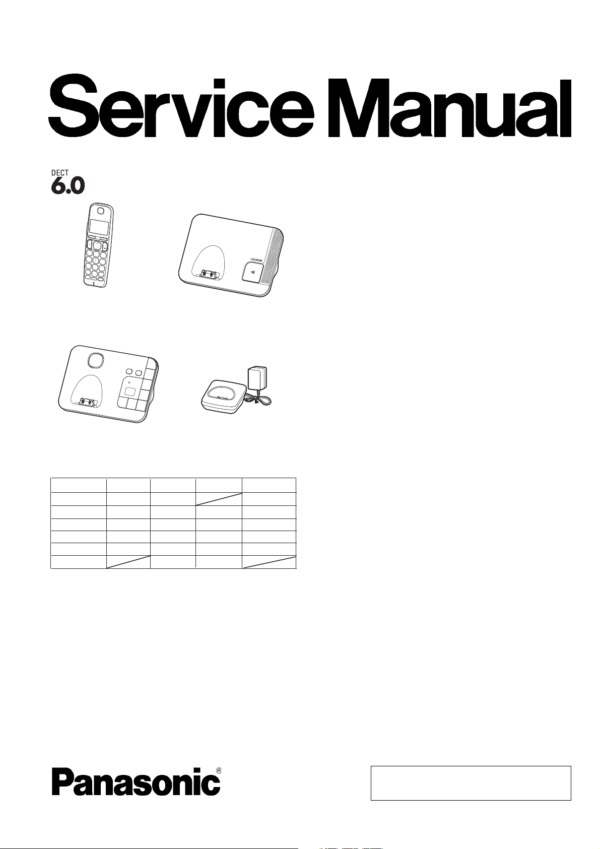
Panasonic KX-TGE212B, KX-TGE233B, KX-TGE232B, KX-TGE210B, KX-TGEA20B User Manual
...
ORDER NO. KM41401789CE
Telephone Equipment
Model No. KX-TGE210B
KX-TGE212B
KX-TGE232B
KX-TGE233B
KX-TGE234B
F13
KX-TGEA20
(Handset)
KX-TGE230
(Base Unit)
Configuration for each model
Model No
KX-TGE210
KX-TGE212
KX-TGE232
KX-TGE233
KX-TGE234
KX-TGEA20*
*KX-TGEA20 is also an optional accessory, which contains a
handset and a charger.
Base Unit Handset
1 (TGE210) 1 (TGEA20)
1 (TGE210) 2 (TGEA20) 1
1 (TGE230) 2 (TGEA20) 1
1 (TGE230) 3 (TGEA20) 2
1 (TGE230) 4 (TGEA20) 3
1 (TGEA20) 1
KX-TGE210
(Base Unit)
(Charger Unit)
Charger Unit Expandable
Up to 6
Up to 6
Up to 6
Up to 6
Up to 6
KX-TGEA20B
Digital Cordless Phone
Digital Cordless Answering System
B: Black Version
(for U.S.A.)
© Panasonic System Networks Co., Ltd. 2014
Unauthorized copying and distribution is a violation
of law.

KX-TGE210/KX-TGE212/KX-TGE232/KX-TGE233/KX-TGE234/TGEA20
WARNING
This service information is designed for experienced repair technicians only and is not designed for use by the general
public. It does not contain warnings or cautions to advise non-technical individuals of potential dangers in attempting
to service a product. Products powered by electricity should be serviced or repaired only by experienced professional
technicians. Any attempt to service or repair the product or products dealt with in this service information by anyone
else could result in serious injury or death.
IMPORTANT SAFETY NOTICE
There are special components used in this equipment which are important for safety. These parts are marked by
in the Schematic Diagrams, Circuit Board Diagrams, Exploded Views and Replacement Parts List. It is essential that
these critical parts should be replaced with manufacturer’s specified parts to prevent shock, fire or other hazards.
Do not modify the original design without permission of manufacturer.
IMPORTANT INFORMATION ABOUT LEAD FREE, (PbF), SOLDERING
If lead free solder was used in the manufacture of this product, the printed circuit boards will be marked PbF.
Standard leaded, (Pb), solder can be used as usual on boards without the PbF mark.
When this mark does appear, please read and follow the special instructions described in this manual on the
use of PbF and how it might be permissible to use Pb solder during service and repair work.
L When you note the serial number, write down all 11 digits. The serial number may be found on the bottom of the unit.
L The illustrations in this Service Manual may vary slightly from the actual product.
2

TABLE OF CONTENTS
1 Safety Precautions ----------------------------------------------- 5
1.1. For Service Technicians --------------------------------- 5
2 Warning-------------------------------------------------------------- 5
2.1. Battery Caution--------------------------------------------- 5
2.2. About Lead Free Solder (PbF: Pb free)-------------- 5
2.2.1. Suggested PbF Solder ------------------------------ 6
2.3. Discarding of P. C. Board-------------------------------- 6
3 Specifications ----------------------------------------------------- 7
4 Technical Descriptions ----------------------------------------- 8
4.1. US-DECT Description ------------------------------------ 8
4.1.1. TDD Frame Format ---------------------------------- 8
4.1.2. TDMA system------------------------------------------ 8
4.1.3. Signal Flowchart in the Radio Parts-------------- 9
4.2. Block Diagram (Base Unit_Main)---------------------10
4.3. Tel Interface Circuit--------------------------------------- 11
4.4. Block Diagram (Base Unit_RF Part) -----------------12
4.5. Circuit Operation (Base Unit) --------------------------13
4.5.1. BBIC (Base Band IC: IC501) ---------------------13
4.5.2. Flash Memory (IC502)------------------------------13
4.5.3. Flash Memory (IC601)------------------------------13
4.5.4. EEPROM (IC611)------------------------------------13
4.5.5. Power Supply Circuit/Reset Circuit--------------14
4.5.6. Telephone Line Interface---------------------------16
4.5.7. Parallel Connection Detect Circuit/Auto
Disconnect Circuit -----------------------------------17
4.5.8. Calling Line Identification (Caller ID)/Call
Waiting Caller ID -------------------------------------18
4.6. Block Diagram (Handset)-------------------------------20
4.7. Block Diagram (Handset_RF Part)-------------------21
4.8. Circuit Operation (Handset)----------------------------22
4.8.1. Outline --------------------------------------------------22
4.8.2. Power Supply Circuit/Reset Circuit--------------22
4.8.3. Charge Circuit ----------------------------------------23
4.8.4. Battery Low/Power Down Detector--------------23
4.8.5. Speakerphone ----------------------------------------23
4.9. Behavior of Electric Power Failure -------------------24
4.10. Circuit Operation (Charger Unit) ----------------------24
5 Location of Controls and Components ------------------25
6 Installation Instructions ---------------------------------------25
7 Operating Instructions-----------------------------------------25
8 Test Mode ----------------------------------------------------------26
8.1. Engineering Mode ----------------------------------------26
8.1.1. Base Unit ----------------------------------------------26
8.1.2. Handset ------------------------------------------------28
9 Service Mode -----------------------------------------------------30
9.1. How to Clear User Setting (Handset Only)---------30
10 Troubleshooting Guide ----------------------------------------31
10.1. Troubleshooting Flowchart -----------------------------31
10.1.1. Check Power------------------------------------------32
10.1.2. Check Record ----------------------------------------33
10.1.3. Check Playback -------------------------------------36
10.1.4. Check Battery Charge ------------------------------36
10.1.5. Check Link---------------------------------------------37
10.1.6. Check the RF part -----------------------------------39
10.1.7. Registering a Handset to the Base Unit--------43
10.1.8. Deregistering a Handset ---------------------------43
10.1.9. Check Handset Transmission --------------------44
10.1.10. Check Handset Reception-------------------------44
KX-TGE210/KX-TGE212/KX-TGE232/KX-TGE233/KX-TGE234/TGEA20
PAG E PAG E
10.1.11. Check Caller ID ------------------------------------- 44
11 Disassembly and Assembly Instructions--------------- 45
11.1. Disassembly Instructions------------------------------- 45
11.1.1. Base Unit ---------------------------------------------- 45
11.1.2. Handset------------------------------------------------ 49
11.1.3. Charger Unit ------------------------------------------ 50
11.2. How to Replace the Handset LCD------------------- 51
12 Measurements and Adjustments -------------------------- 52
12.1. Equipment Required ------------------------------------ 52
12.2. The Setting Method of JIG----------------------------- 52
12.2.1. Connections (Base Unit) -------------------------- 52
12.2.2. Connections (Handset) ---------------------------- 53
12.2.3. How to install Batch file into P.C. ---------------- 54
12.2.4. Commands-------------------------------------------- 55
12.3. Adjustment Standard (Base Unit) -------------------- 56
12.3.1. Bottom View ------------------------------------------ 56
12.4. Adjustment Standard (Handset)---------------------- 57
12.4.1. Component View ------------------------------------ 57
12.5. Things to Do after Replacing IC or X'tal------------ 58
12.5.1. How to download the data ------------------------ 58
12.6. Frequency Table------------------------------------------ 59
13 Miscellaneous ---------------------------------------------------- 60
13.1. How to Replace the LLP (Leadless Leadframe
Package) IC ----------------------------------------------- 60
13.1.1. Preparation-------------------------------------------- 60
13.1.2. Caution------------------------------------------------- 60
13.1.3. How to Remove the IC ----------------------------- 60
13.1.4. How to Install the IC -------------------------------- 61
13.2. How to Replace the Flat Package IC --------------- 62
13.2.1. Preparation-------------------------------------------- 62
13.2.2. How to Remove the IC ----------------------------- 62
13.2.3. How to Install the IC -------------------------------- 63
13.2.4. How to Remove a Solder Bridge ---------------- 63
13.3. Terminal Guide of the ICs, Transistors and
Diodes ------------------------------------------------------ 64
13.3.1. Base Unit ---------------------------------------------- 64
13.3.2. Handset ------------------------------------------------ 64
14 Schematic Diagram -------------------------------------------- 66
14.1. For Schematic Diagram -------------------------------- 66
14.1.1. Base Unit (Schematic Diagram (Base
Unit_Main)) ------------------------------------------- 66
14.1.2. Handset (Schematic Diagram
(Handset_Main))------------------------------------- 66
14.2. Schematic Diagram (Base Unit_Main)-------------- 67
14.2.1. KX-TGE210 ------------------------------------------- 67
14.2.2. KX-TGE230 ------------------------------------------- 69
14.3. Schematic Diagram (Base Unit_Operation) ------- 71
14.3.1. KX-TGE230 ------------------------------------------- 71
14.4. Schematic Diagram (Handset_Main) --------------- 73
15 Printed Circuit Board ------------------------------------------ 76
15.1. Circuit Board (Base Unit_Main) ---------------------- 76
15.1.1. Component View ------------------------------------ 76
15.1.2. Bottom View ------------------------------------------ 77
15.2. Circuit Board (Base Unit_Operation)---------------- 78
15.2.1. KX-TGE230 ------------------------------------------- 78
15.3. Circuit Board (Handset_Main) ------------------------ 80
15.3.1. Component View ------------------------------------ 80
15.3.2. Bottom View ------------------------------------------ 81
3

KX-TGE210/KX-TGE212/KX-TGE232/KX-TGE233/KX-TGE234/TGEA20
16 Exploded View and Replacement Parts List -----------82
16.1. Cabinet and Electrical Parts (Base Unit) ----------- 82
16.1.1. KX-TGE210 ------------------------------------------- 82
16.1.2. KX-TGE230 ------------------------------------------- 83
16.2. Cabinet and Electrical Parts (Handset) ------------- 84
16.3. Cabinet and Electrical Parts (Charger Unit) ------- 85
16.4. Accessories and Packing Materials ----------------- 86
16.4.1. KX-TGE210B ----------------------------------------- 86
16.4.2. KX-TGE212B ----------------------------------------- 87
16.4.3. KX-TGE232B ----------------------------------------- 88
16.4.4. KX-TGE233B ----------------------------------------- 89
16.4.5. KX-TGE234B ----------------------------------------- 90
16.5. Replacement Parts List --------------------------------- 91
16.5.1. Base Unit ----------------------------------------------91
16.5.2. Handset ------------------------------------------------ 94
16.5.3. Charger Unit ------------------------------------------95
16.5.4. Accessories and Packing Materials------------- 95
16.5.5. Screws ------------------------------------------------- 96
16.5.6. Fixtures and Tools ----------------------------------- 96
4
KX-TGE210/KX-TGE212/KX-TGE232/KX-TGE233/KX-TGE234/TGEA20
Component
Component
pin
Solder
Remove all of the
excess solder
(Slice View)
1 Safety Precautions
1.1. For Service Technicians
• Repair service shall be provided in accordance with repair technology information such as service manual so as to
prevent fires, injury or electric shock, which can be caused by improper repair work.
1. When repair services are provided, neither the products nor their parts or members shall be remodeled.
2. If a lead wire assembly is supplied as a repair part, the lead wire assembly shall be replaced.
3. FASTON terminals shall be plugged straight in and unplugged straight out.
• ICs and LSIs are vulnerable to static electricity.
When repairing, the following precautions will help prevent recurring malfunctions.
1. Cover plastic parts boxes with aluminum foil.
2. Ground the soldering irons.
3. Use a conductive mat on worktable.
4. Do not grasp IC or LSI pins with bare fingers.
2Warning
2.1. Battery Caution
Risk of explosion if battery is replaced by an incorrect type. Dispose of used batteries according to the instructions.
Attention:
A nickel metal hydride battery that is recyclable powers the product you have purchased.
Please call 1-800-8-BATTERY (1-800-822-8837) for information on how to recycle this battery.
2.2. About Lead Free Solder (PbF: Pb free)
Note:
In the information below, Pb, the symbol for lead in the periodic table of elements, will refer to standard solder or solder that
contains lead.
We will use PbF solder when discussing the lead free solder used in our manufacturing process which is made from Tin (Sn),
Silver (Ag), and Copper (Cu).
This model, and others like it, manufactured using lead free solder will have PbF stamped on the PCB. For service and repair
work we suggest using the same type of solder.
Caution
• PbF solder has a melting point that is 50 F ~ 70 F (30 C ~ 40 C) higher than Pb solder. Please use a soldering iron with
temperature control and adjust it to 700 F ± 20 F (370 C ± 10 C).
• Exercise care while using higher temperature soldering irons.:
Do not heat the PCB for too long time in order to prevent solder splash or damage to the PCB.
• PbF solder will tend to splash if it is heated much higher than its melting point, approximately 1100 F (600 C).
• When applying PbF solder to double layered boards, please check the component side for excess which may flow onto the
opposite side (See the figure below).
5
KX-TGE210/KX-TGE212/KX-TGE232/KX-TGE233/KX-TGE234/TGEA20
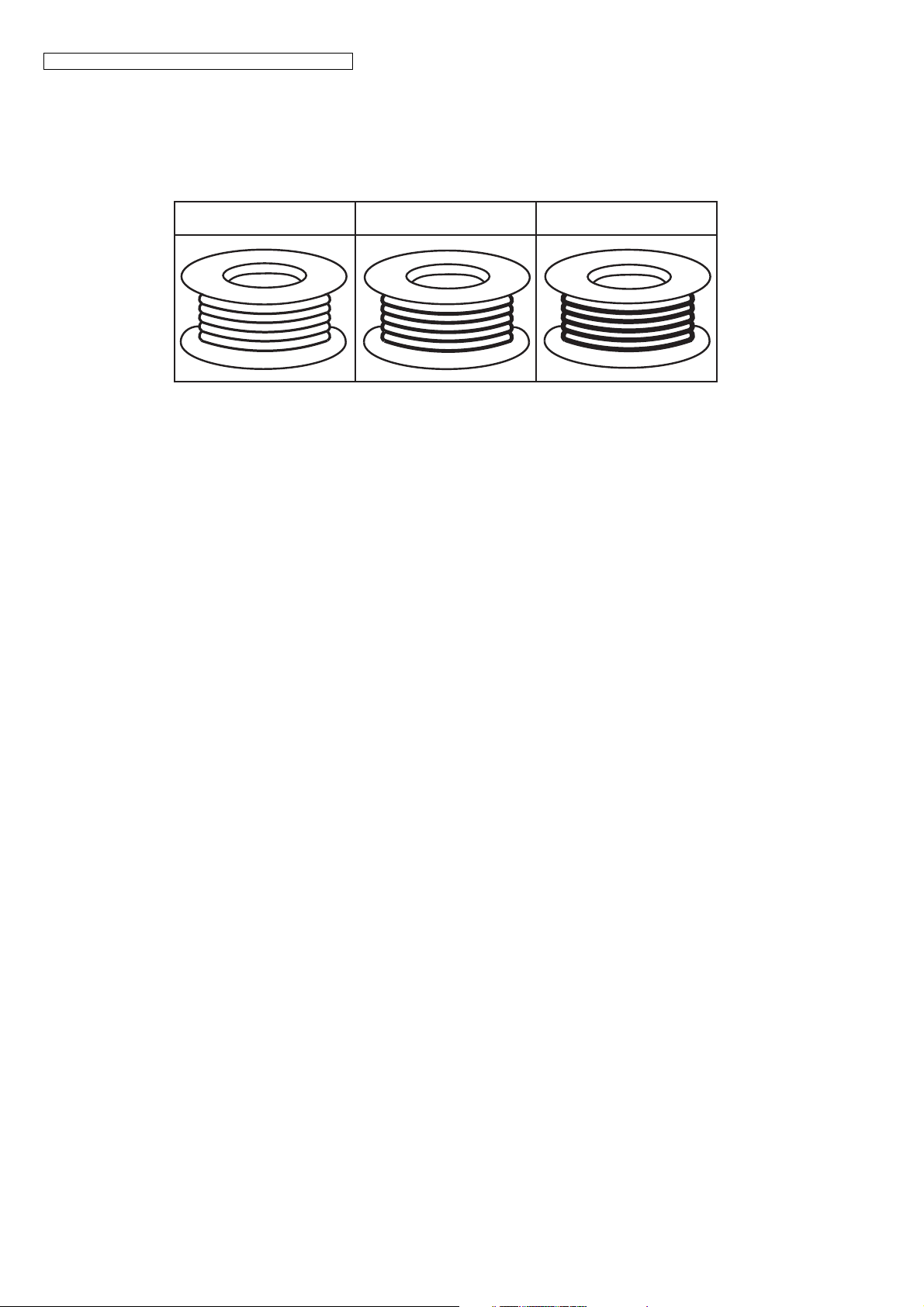
0.3 mm X 100 g
0.6 mm X 100 g 1.0 mm X 100 g
2.2.1. Suggested PbF Solder
There are several types of PbF solder available commercially. While this product is manufactured using Tin, Silver, and Copper
(Sn+Ag+Cu), you can also use Tin and Copper (Sn+Cu), or Tin, Zinc, and Bismuth (Sn+Zn+Bi). Please check the
manufacturer's specific instructions for the melting points of their products and any precautions for using their product with other
materials.
The following lead free (PbF) solder wire sizes are recommended for service of this product: 0.3 mm, 0.6 mm and 1.0 mm.
2.3. Discarding of P. C. Board
When discarding P. C. Board, delete all personal information such as telephone directory and caller list or scrap P. C. Board.
6
3 Specifications
Rechargeable Ni-MH battery
AAA (R03) size (1.2 V 400 mAh)
Super Heterodyne
PLL synthesizer
Quadrature Discriminator
13.824 MHz ±100 Hz
Frequency Modulation
40 bit
Tone (DTMF)/Pulse
Up to 48 digits
Up to 24 digits
(Phonebook)
8 days at Standby,
10 hours at Talk
8 days at Standby,
10 hours at Talk
Approx. 130
0 °C - 40 °C (32 °F – 104 °F)
20 % – 80 % relative air humidity
(dry)
Approx. 54
mm x 31 mm x
171
mm
Approx. 130 g
Power source
Receiving Method
Oscillation Method
Detecting Method
Tolerance of OSC Frequency
Modulation Method
ID Code
Ringer Equivalence No. (REN)
Dialing Mode
Redial
Speed Dialer
Power Consumption
Operating Conditions
Dimensions (W x D x H)
Mass (Weight)
AC Adaptor
(PNLV226Z, 120 V AC, 60 Hz)
Super Heterodyne
PLL synthesizer
Quadrature Discriminator
10.368 MHz ±41 Hz
Frequency Modulation
40 bit
0.1B
Tone (DTMF)/Pulse
Up to 48 digits
Up to 24 digits (Phonebook)
Base Unit*1
Standby: Approx. 1.0 W
Maximum: Approx. 4.3 W
Base Unit*2
Standby: Approx. 1.0 W
Maximum: Approx. 4.3 W
0 °C - 40 °C (32 °F – 104 °F)
20 % – 80 % relative air humidity
(dry)
Approx. 197 mm x 88 mm x 83 mm
Approx. 270 g
Base Unit
Handset
Charger
AC Adaptor
(PNLV233AZ, 120 V AC, 60 Hz)
Standby: Approx 0.1 W
Maximum: Approx 1.8 W
Standby: Approx 0.1 W
Maximum: Approx 1.8 W
0 °C - 40 °C (32 °F – 104 °F)
20 % – 80 % relative air humidity
(dry)
Approx. 72 mm x 72 mm x 38 mm
Approx. 90 g
*1 KX-TGE210 series
*2 KX-TGE230 series
Duplex procedure:
TDMA (Time Division Multiple Access)
█ Channel spacing:
1.728MHz (DECT 6.0)
█ Bit rate:
1.152Mbit/s (DECT 6.0)
Modulation:
GFSK (Gaussian Frequency Shift Keying)
RF transmission power:
115 mW (max/DECT6.0)
Voice coding:
ADPCM 32 kbit/s (DECT 6.0)
█
█
█
█
█
█
█ Standard:
DECT 6.0 (Digital Enhanced Cordless
Telecommunications 6.0)
█ Number of channels:
60 Duplex Channels (DECT 6.0)
█ Frequency range:
1.92 GHz to 1.93 GHz (DECT 6.0)
KX-TGE210/KX-TGE212/KX-TGE232/KX-TGE233/KX-TGE234/TGEA20
Note:
Design and specifications are subject to change without notice.
Note for Service:
• Operation range: Up to 300 m outdoors, Up to 50 m indoors, depending on the condition.
• Analog telephone connection: Telephone Line
• Optional headset: KX-TCA60, KX-TCA93, KX-TCA400, KX-TCA430
• Optional Range extender: KX-TGA405
• Optional Key detector: KX-TGA20
• T-adaptor: KX-J66
7
KX-TGE210/KX-TGE212/KX-TGE232/KX-TGE233/KX-TGE234/TGEA20
4 Technical Descriptions
4.1. US-DECT Description
The frequency range of 1.92 GHz-1.93 GHz is used. Transmitting and receiving carrier between base unit and handset is same
frequency. Refer to Frequency Table (P.59).
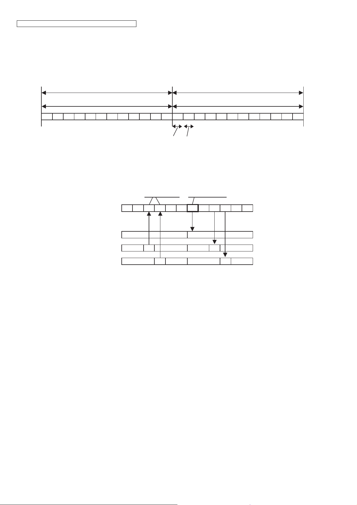
4.1.1. TDD Frame Format
5 ms 5 ms
Up Link ( Handset -> Base Unit ) Down Link ( Base Unit -> Handset )
RX1 RX2 RX3 RX4 RX5 RX6 TX1 TX2 TX3 TX4 TX5 TX6
DATA rate : 1.152 Mbps
417 μs (available) 417 μs (blind)
4.1.2. TDMA system
This system is the cycles of 10 ms, and has 6 duplex paths, but maximum duplex communication path is 5 because of dummy
bearer use.
In 1 slot 417 s, the 10 ms of voice data is transmitted.
• 2 - Handsets Link
Traffic Bearer Dummy bearer
Base unit
Handset 1
(Stand by)
Handset 2
(Link)
Handset 3
(Link)
Traffic Bearer
A link is established between base unit and handset.
The state where duplex communication is performed.
Handset doesn't make up duplex in no free RF channels because of interference. (*1)
Dummy Bearer
Base unit sends Dummy-data to the all stand-by state handsets.
Handsets receive that data for synchronization and monitoring request from the base unit.
Base unit doesn't send Dummy bearer in no free RF channels because of interference. (*1)
Note:
(*1) It is a feature under FCC 15 regulation and for interference avoidance.
In the case of checking RF parts, it is better in least interference condition.
RX1 RX2 RX3 RX4 RX5 RX6 TX1 TX2 TX3 TX4 TX5 TX6
TX RX
RXTX
8

KX-TGE210/KX-TGE212/KX-TGE232/KX-TGE233/KX-TGE234/TGEA20
4.1.3. Signal Flowchart in the Radio Parts
Reception
Base unit:
A voice signal from TEL line is encoded to digital data and converted into a 1.9GHz modulated radio signal by BBIC(IC501).
The RF signal, after which is amplified in BBIC, is fed to selected antenna.
Handset:
As for a handset RF, RF signal is received in one antenna.
BBIC down-converts to 864 kHz IF signal from RX signal and demodulates it to digital data "RXDATA".
BBIC (IC1) converts RXDATA into a voice signal and outputs it to speaker.
Transmission
Handset:
A voice signal from microphone is encoded to digital data and converted into a 1.9GHz modulated radio signal by BBIC(IC1).
The RF signal, after which is amplified in BBIC, is fed to an antenna.
Base unit:
As for a base unit RF, RF signal is received in two antennas.
BBIC (IC501) compares RF signal levels and selects the antenna to be used. Then BBIC down-converts to 864 kHz IF signal
from RX signal in the selected antenna, and demodulates it to digital data "RXDATA".
BBIC (IC501) converts RXDATA into a voice signal and outputs it to TEL line.
9
KX-TGE210/KX-TGE212/KX-TGE232/KX-TGE233/KX-TGE234/TGEA20
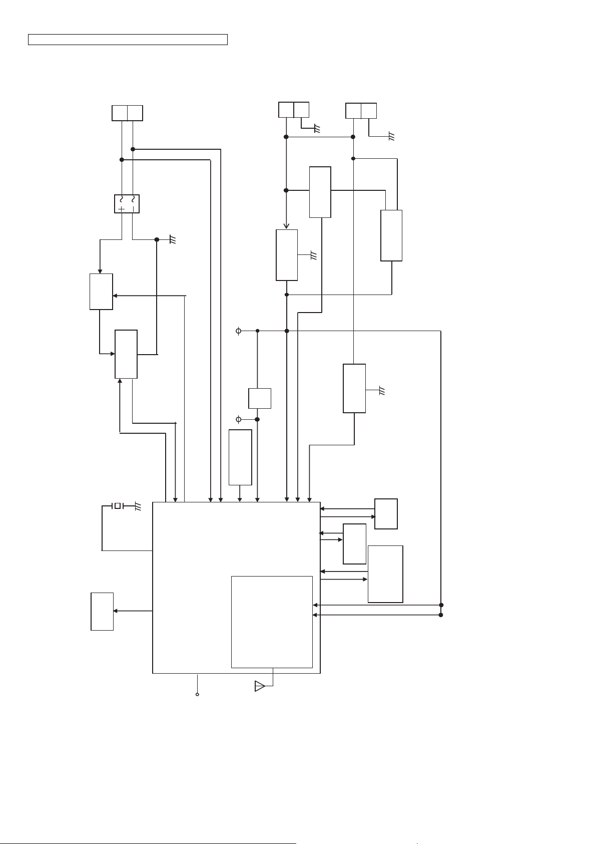
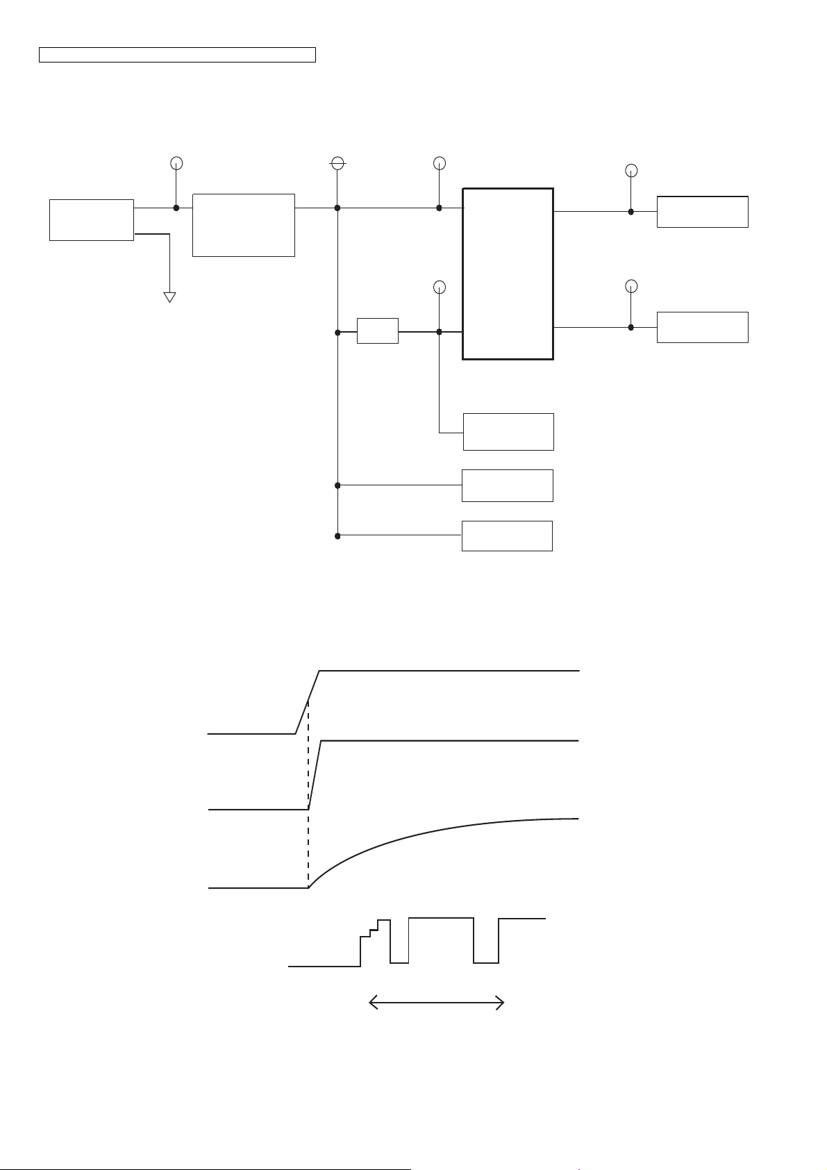
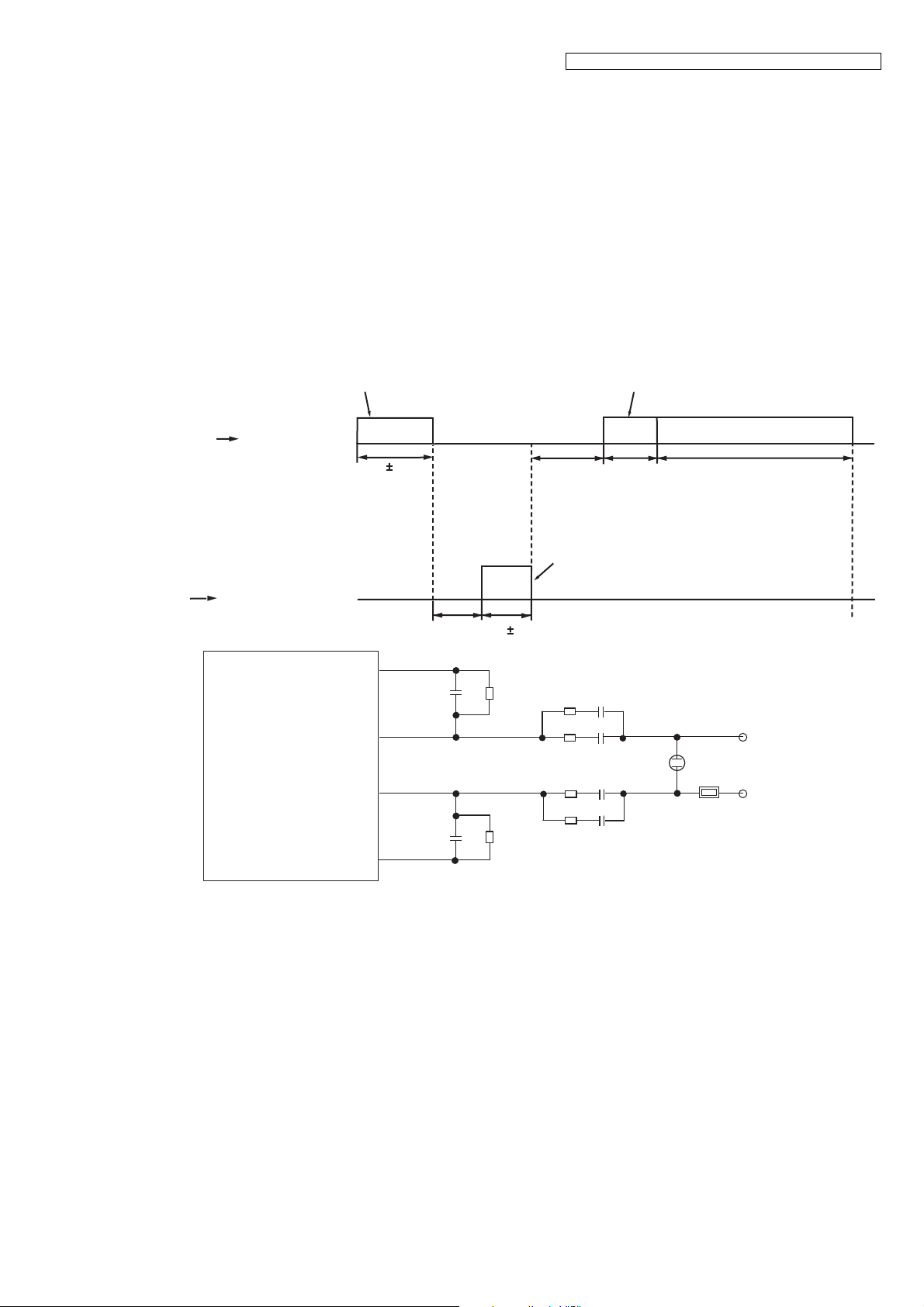
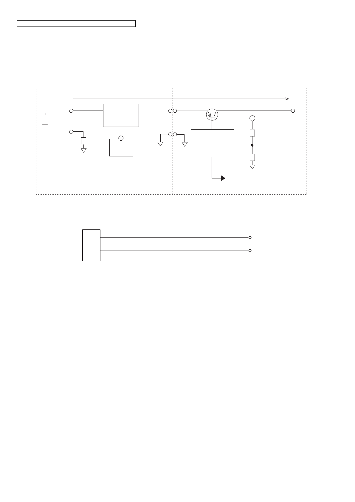
KX-TGE210/212/232/233/234 BLOCK DIAGRAM (Base Unit_Main)
SIDE_TONE
CIRCUIT
Crystal
10.368MHz
TR_RLY
TIP
RING
RF_Block
IC501
BBIC
DC5.5V+
GND
DC_JACK
+
-
CHARGE
3
4
2
D101
CHARGE
DETECT
Q701
REGULATOR
IC302
Power Down
DET
Power supply
at AC failure
KEY
PAD
LED
VBAT
PDN_DET
CHARGE_DET
IC611
Q301
+1.8V
+3.0V
AVD/VDD
QSPI
CIDINp
CIDINn
P3_6
MICh
LSRp
RF_VDD
VDD_PA
ANT1
IC502
Flash(Program)
IC601
Flash
(Voice prompt)
EEPROM
4.2. Block Diagram (Base Unit_Main)
10

4.3. Tel Interface Circuit
TX AMP
SIDE TONE
RX AMP
CONTROL
CIRCUIT
CALLER ID
DETECT
BELL
DETECT
P101
R142
4
C101
Q141
C102
SA101
TIP
R141
REGULATOR
C104
R102
C106
R104
C103
R101
C105
R103
D101
KX-TGE210/KX-TGE212/KX-TGE232/KX-TGE233/KX-TGE234/TGEA20
11
KX-TGE210/KX-TGE212/KX-TGE232/KX-TGE233/KX-TGE234/TGEA20
10.368
MHz
IC501 RF block
TXDATA
RF_TXp
RF_TXn
RF_RXp
RF_RXn
Control
Logic
RXDATA
Mixer
Demodulator
PLL
3856-3843MHz
/3859-3845MHz
Modulator
KX-TGE210/212/232/233/234 BLOCK DIAGRAM (Base Unit_RF Part)
4.4. Block Diagram (Base Unit_RF Part)
12
KX-TGE210/KX-TGE212/KX-TGE232/KX-TGE233/KX-TGE234/TGEA20
4.5. Circuit Operation (Base Unit)
General Description:
(BBIC, Flash Memory, EERROM) is a digital speech/signal processing system that implements all the functions of speech
compression, record and playback, and memory management required in a digital telephone answering machine.
The BBIC system is fully controlled by a host processor. The host processor provides activation and control of all that functions
as follows.
ADPCM
ADPCM
Caller ID
Modem
Digital TAM System
Flash Memory IC601
Digital
Speech
Processor
Analog
Front
End
&
Multiplexer
TEL
Line
Interface
SP
RF part
EEPROM
IC611
TDD & TDMA
with FHSS
Processor
Keys/ LEDs
/ Charge
Host CPU
BBIC (IC501)
Flash Memory
(Program)
IC502
4.5.1. BBIC (Base Band IC: IC501)
• Voice Message Recording/Play back
The BBIC system uses a proprietary speech compression technique to record and store voice message in Flash Memory.
An error correction algorithm is used to enable playback of these messages from the Flash Memory.
• DTMF Generator
When the DTMF data from the handset is received, the DTMF signal is output.
• Synthesized Voice (Pre-recorded message)
The BBIC implements synthesized Voice, utilizing the built in speech detector and a Flash Memory, which stored the vocabulary.
• Caller ID demodulation
The BBIC implements monitor and demodulate the FSK/DTMF signals that provide CID information from the Central Office.
• Digital Switching
The voice signal from telephone line is transmitted to the handset or the voice signal from the handset is transmitted to the
Telephone line, etc. They are determined by the signal path route operation of voice signal.
• Block Interface Circuit
RF part, LED, Key scan, Speaker, Telephone line.
4.5.2. Flash Memory (IC502)
Main program data is stored.
4.5.3. Flash Memory (IC601)
Following information data is stored.
• Voice signal
ex: Pre-recorded Greeting message, Incoming message
4.5.4. EEPROM (IC611)
Following information data is stored.
• Settings
ex: message numbers, ID code, Flash Time, Tone/Pulse
13
KX-TGE210/KX-TGE212/KX-TGE232/KX-TGE233/KX-TGE234/TGEA20
+5.5V
+5.5V +3.0V
+3.0V
+1.8V
+3.0V_CP
IC501
IC302
IC611
BBIC
AC Adaptor
3.0V
REGULATOR
EEPROM
VDD3
VDD1
VDD4
+3.0V_CP2
IC601
TAM FLASH
VDD5
RF Part
LEDs
Q301
QSPI FLASH
IC502
Startmonitor
(IC501 57pin)
VDD1 (1.8 V)
VBAT
Reset (RSTN)
(IC501_77pin)
BBIC chip initialize
(CKM/STM)
4.5.5. Power Supply Circuit/Reset Circuit
The power supply voltage from AC adaptor is converted to VBAT (3.0V) in IC302. And +3.0V for peripherals and analog part is
insulated from VBAT by Doubler of BBIC.
Circuit Operation:
14
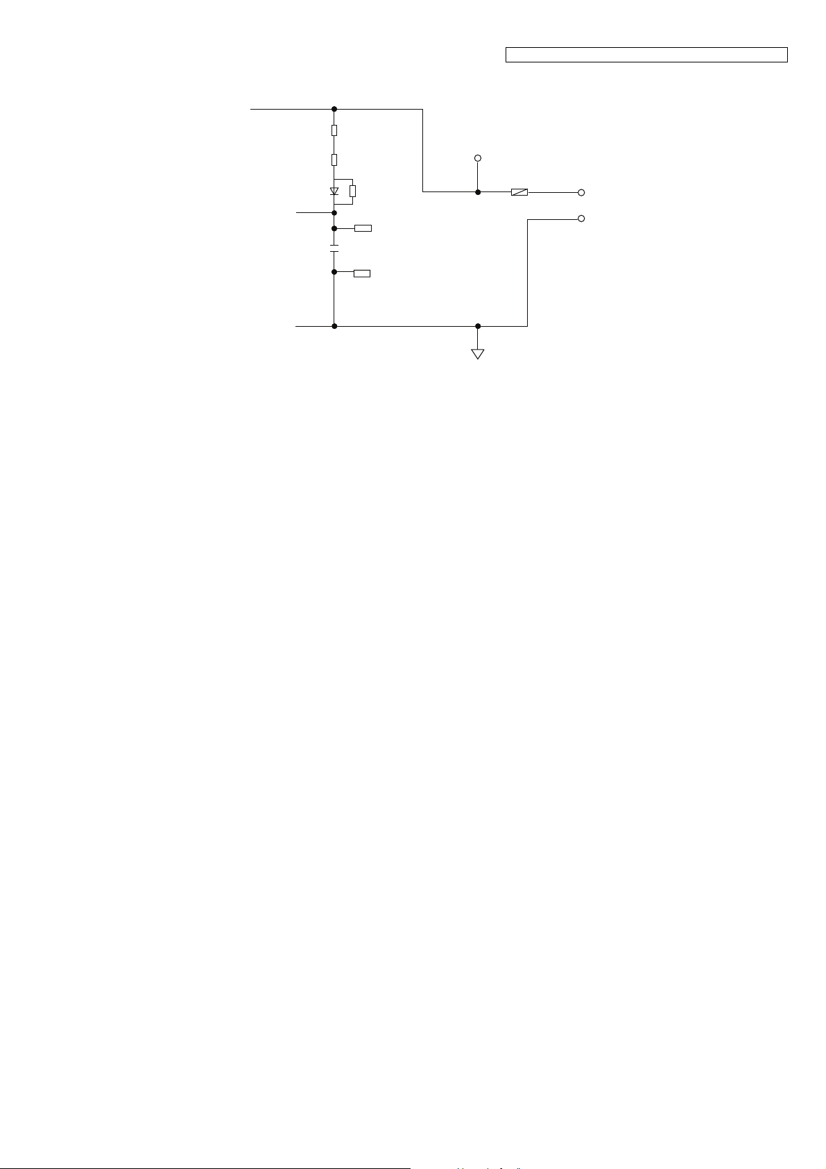
4.5.5.1. Charge Circuit
R372
D362
R371
CHARGE+
R373
C351
F301
DCP
CHARGE-
+5.5V
DCM
K A
The voltage from the AC adaptor is supplied to the charge circuits.
KX-TGE210/KX-TGE212/KX-TGE232/KX-TGE233/KX-TGE234/TGEA20
15
KX-TGE210/KX-TGE212/KX-TGE232/KX-TGE233/KX-TGE234/TGEA20
OFF Hook
BELL signal detection
C174
C171
R166
R178
RX
Pin25 of IC501
TX
Pin27 of IC501
R160
+
C161
C167
R165
R162
C173
R151R164
C184
C103
C111
Q161
E
B
C
R163
R117
C115
R109
C109
Q141
Q142
C101
P101
L1T
L1R
D101
C102
1
2
3
+
~~
_
4
R145
C142
C152
R152
A
K
D142
R141
B
E
C
E
B
C
R142
SA101
R111
R101
HOOK
Pin19 of IC501
CIDOUT
Pin24 of IC501
LSRn
Pin28 of IC501
RINGING
Pin18 of IC501
CIDINn
Pin23 of IC501
CIDINp
Pin21 of IC501
R168
PARADET
Pin17 of IC501
ADC1
Pin33 of IC501
ADC0
Pin32 of IC501
R118
C116
R115
R116
R110
C110
R112
C113
C105
R103
C104
R102
C106
R104
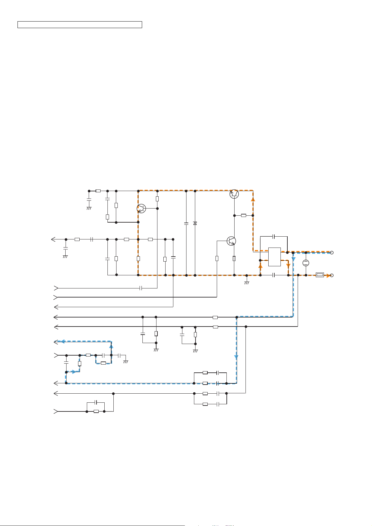
4.5.6. Telephone Line Interface
Telephone Line Interface Circuit:
Function
• Bell signal detection
• ON/OFF hook and pulse dial circuit
• Side tone circuit
Bell (RINGING) signal detection and OFF HOOK circuit:
In the idle mode, Q141 is open to cut the DC loop current and decrease the ring load. When ring voltage appears at the Tip (T)
and Ring (R) leads (When the telephone rings), the AC ring voltage is transferred as follows:
L1T C105 R103 R110 R11 1 R112 BBIC pin18(RINGING)
When the CPU (BBIC) detects a ring signal, Q141 turns on, thus providing an off-hook condition (active DC current flow through
the circuit). Following signal flow is the DC current flow.
T D101 Q141 Q161 R163 D101 P101 R
ON HOOK Circuit:
Q141 is open, Q141 is connected as to cut the DC loop current and to cut the voice signal. The unit is consequently in an onhook condition.
Pulse Dial Circuit:
Pin 19 of BBIC turns Q141 ON/OFF to make the pulse dialing.
Side Tone Circuit:
Basically this circuit prevents the TX signal from feeding back to RX signal. As for this unit, TX signal feed back from Q161 is
canceled by the canceller circuit of BBIC.
16
KX-TGE210/KX-TGE212/KX-TGE232/KX-TGE233/KX-TGE234/TGEA20
C174
C171
R166
R178
RX
Pin25 of IC501
TX
Pin27 of IC501
R160
+
C161
C167
R165
R162
C173
R151R164
C184
Q161
E
B
C
R163
R117
C115
Q141
Q142
C101
P101
L1T
L1R
D101
C102
1
2
3
+
~~
_
4
R145
C142
C152
R152
A
K
D142
R141
B
E
C
E
B
C
R142
SA101
HOOK
Pin19 of IC501
R168
PARADET
Pin17 of IC501
ADC1
Pin33 of IC501
ADC0
Pin32 of IC501
R118
C116
R115
R116
4.5.7. Parallel Connection Detect Circuit/Auto Disconnect Circuit
Function:
In order to disable call waiting and stutter tone functions when using telephones connected in parallel, it is necessary to have a
circuit that judges whether a telephone connected in parallel is in use or not. This circuit determines whether the telephone
connected in parallel is on hook or off hook by detecting changes in the T/R voltage.
Circuit Operation:
Parallel connection detection when on hook:
When on hook, the voltage is monitored at pin 32 of IC501. There is no parallel connection if the voltage is
0.54 V or higher, while a parallel connection is deemed to exist if the voltage is lower.
Parallel connection detection when off hook:
When off hook, the voltage is monitored at pin 17 of IC501; the presence/absence of a parallel connection is determined by
detecting the voltage changes.
If the Auto disconnect function is ON and statuses are Hold, receiving ICM, OGM transmitting, BBIC disconnects the line after
detecting parallel connection is off hook.
17
KX-TGE210/KX-TGE212/KX-TGE232/KX-TGE233/KX-TGE234/TGEA20
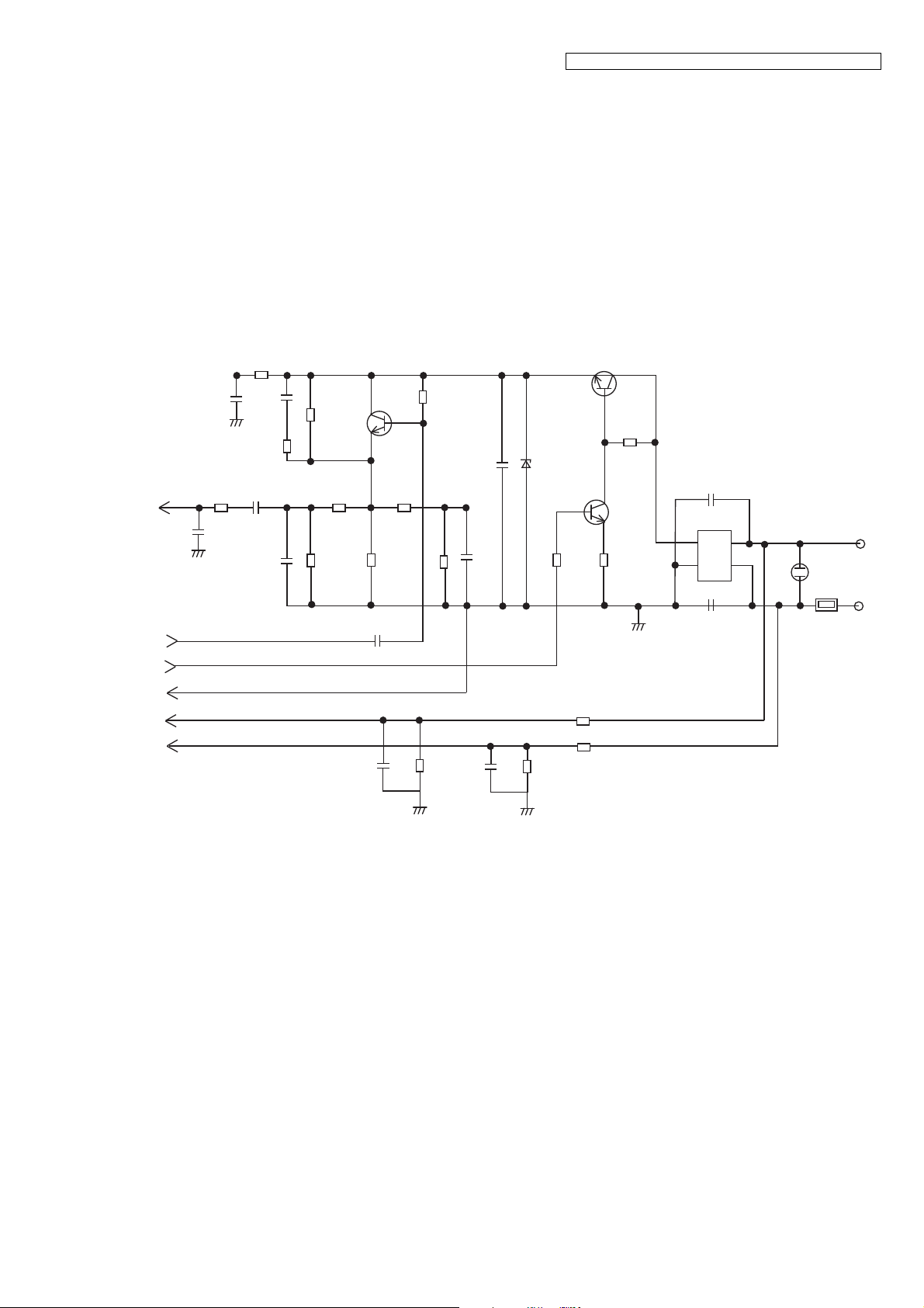
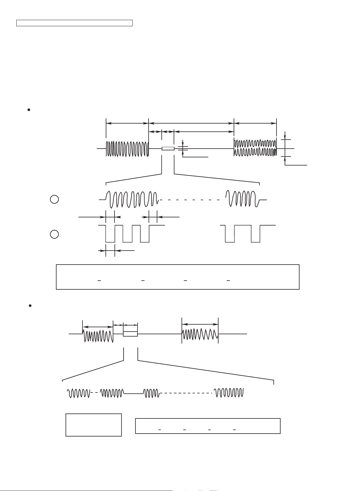
4.5.8. Calling Line Identification (Caller ID)/Call Waiting Caller ID
Function:
Caller ID
The caller ID is a chargeable ID which the user of a telephone circuit obtains by entering a contract with the telephone company
to utilize a caller ID service. For this reason, the operation of this circuit assumes that a caller ID service contract has been
entered for the circuit being used. The data for the caller ID from the telephone exchange is sent during the interval between the
first and second rings of the bell signal. The data from the telephone exchange is a modem signal which is modulated in an FSK
(Frequency Shift Keying) * format. Data
the message format which can be received: i.e. the single message format and plural message format. The plural message
format allows to transmit the name and data code information in addition to the time and telephone number data.
*: Also the telephone exchange service provides other formats.
Single message format
"1" is a 1200 Hz sine wave, and data "0" is a 2200 Hz sine wave. There are two types of
1st Ring
2 sec
0.5 s 575 ms
Silent interval 4 sec
min 0.5 s
2nd Ring
2 sec
STD Ring / 20 Hz
Tip-Ring
DATA in
A
1200 Hz
=DATA "1"
DATA out
B
month day hour minute number
Plural message format
DATA
0.1 Vrms
70 Vrms
2200 Hz
=DATA "0 "
1 bit=833 µs
201348700035161504
1st Ring
2 sec
0.5 s
DATA CODE NAME
201 John Smith
718 ms
DATA
month
04
18
day
2nd Ring
hour
16
minute
number
20134870003516
KX-TGE210/KX-TGE212/KX-TGE232/KX-TGE233/KX-TGE234/TGEA20
CAS
CAS: CPE Alerting Signal
Dual Tone of 2130 Hz, 2750 Hz
-15 dBm (900 ohm load)
80 5 ms
MARK
DATA
0~500 ms
58~75 ms about 300 ms
(be changed by
Information Volume)
Continuance Signal
of 1200 Hz (Data "1")
"FSK"
ACK: Acknowledged Signal
DTMF
"D"
ACK
0~100 ms
60 5 ms
Telephone Exchange
Cordless phone
Cordless phone
Signal Flow
Signal Flow
Telephone Exchange
Call Waiting Format
Call Waiting Caller ID
Calling Identity Delivery on Call Waiting (CIDCW) is a CLASS service that allows a customer, while off-hook on an existing call,
to receive information about a calling party on a waited call. The transmission of the calling information takes place almost
immediately after the customer is alerted to the new call so he/she can use this information to decide whether to take the new
call.
Function:
The telephone exchange transmits or receives CAS and ACK signals through each voice RX/TX route. Then FSK data and
MARK data pass the following route.
Telephone Line P101 C105, C104 R103, R104 RA101 IC501(23, 21).
If the unit deems that a telephone connected in parallel is in use, ACK is not returned even if CAS is received, and the
information for the second and subsequent callers is not displayed on the portable handset display.
IC501
CIDOUT
Pin 24
CIDINn
Pin 23
CIDINp
Pin 21
LSRn
Pin 28
C110
C109
R110
R109
R101
R103
R102
R104
C103
C105
C104
C106
SA101
P101
L1T
L1R
19
KX-TGE210/KX-TGE212/KX-TGE232/KX-TGE233/KX-TGE234/TGEA20
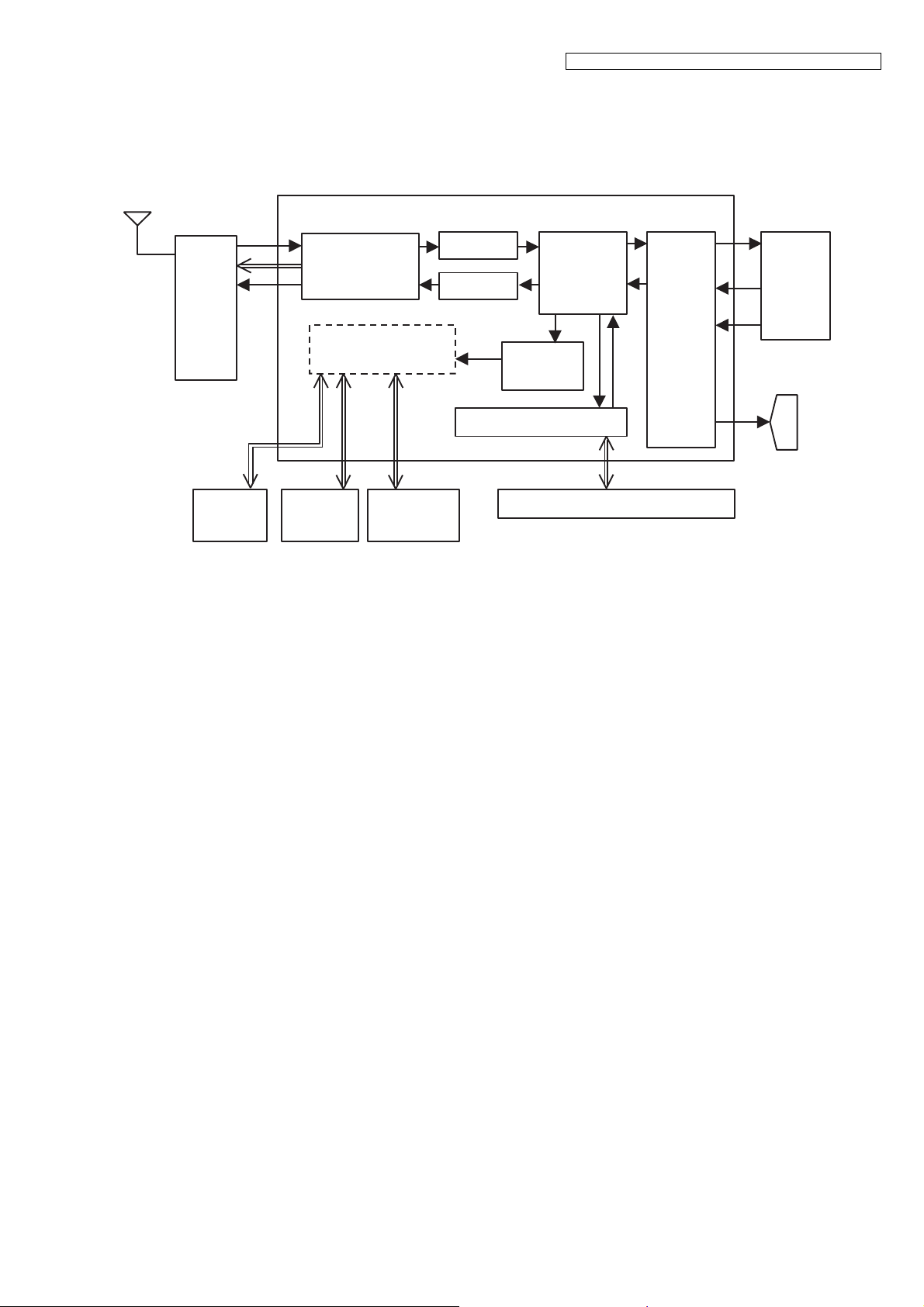
IC1
IC3
MIP
MIN
HSSPOUTP
LOUT
HSMIP
HEADSET_DET
SPOUTP
SPOUTN
CKM//STM
CKM/STM
BBIC
RESET
CHG_CTL
BATTERY_ON
CHG_DET
WP, CLK, DATA
KEYSTOROBE_A~E
KEYIN_1~5
CHARGE
MIC
Receiver
Headset Jack
CN4
Monitor SP
LCD
CHARGE
PUMP
IC4
KEYS
RF part
ANT1
X1
13.824 MHz
EEPROM
3V
BATTERY
LED
(LCD)
RSTN
VBAT
VBAT
3V
4.0V
VBAT
RXn
RXp
TXp
TXn
KX-TGEA20 BLOCK DIAGRAM (Handset)
KEY_LED
CP_OFF
Q6
LED
(KEY)
4V
CHARGE
CONTROL
POWER SUPPLY
CONTROL
4.6. Block Diagram (Handset)
20

4.7. Block Diagram (Handset_RF Part)
ANT
KX-TGE210/KX-TGE212/KX-TGE232/KX-TGE233/KX-TGE234/TGEA20
TXp
TXn
RXp
RXn
KX-TGEA20 BLOCK DIAGRAM (Handset_RF Part)
21

KX-TGE210/KX-TGE212/KX-TGE232/KX-TGE233/KX-TGE234/TGEA20
4.8. Circuit Operation (Handset)
4.8.1. Outline
Handset consists of the following ICs as shown in Block Diagram (Handset) (P.20).
• DECT BBIC (Base Band IC): IC1
- All data signals (forming/analyzing ACK or CMD signal)
- All interfaces (ex: Key, Detector Circuit, Charge, EEPROM, LCD)
• EEPROM: IC3
- Setting data is stored. (e.g. ID, user setting)
4.8.2. Power Supply Circuit/Reset Circuit
Circuit Operation:
When powering on the Handset, the voltage is as follows;
BATTERY(2.2 V ~ 2.6 V: BATT+) F1 BBC1 (IC1) 10 pin
The Reset signal generates IC1 (54 pin) and 1.8 V.
VBAT
VDDC (1.2 V)
GND
VBAT
External Charge Pump
Circuit or IC
Reset (RSTN)
(IC1_54 pin)
Start monitor
(IC1 57pin)
(CKM/STM)
BATTERY
2CELL
VDDC (1.2V)
VBAT
4.0V
BBIC
BBIC chip initialize
3.0V
3.0V
DOUBLER OUT (Charge Pump)
For all peripherals
3.0V3.0V
EEPROM
3.0V3.0V
LCD
4.0 output
LCD BACKLIT LED
3.0V
KEY LED
GND
22
KX-TGE210/KX-TGE212/KX-TGE232/KX-TGE233/KX-TGE234/TGEA20
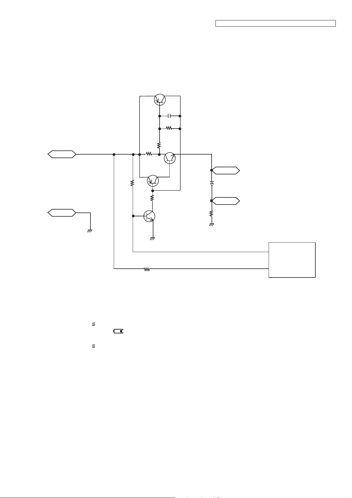
CHG +
Q4
R45
R4
47K
R6
10K
Q9
GND
R7 CHG DET (34)
CHG CTRL (32)
100K
CHG -
GND
BATT +
BATTERY
2CELL
BATT -
GND
BBIC
IC1
Q2
R8
Q3
C27
R2
R9
4.8.3. Charge Circuit
Circuit Operation:
When charging the handset on the Base Unit, the charge current is as follows;
DCP(5.5V) F301 R371 R372 D362 CHARGE+(Base) CHARGE+(Handset) R8 Q3 F1 BATTERY+...
Battery...
BATTERY- R45 GND CHARGE-(Handset) CHARGE-(Base) GND DC-(GND)
In this way, the BBIC on Handset detects the fact that the battery is charged.
The charge current is controlled by switching Q9 of Handset.
Refer to Fig.101 in Power Supply Circuit/Reset Circuit (P.14).
4.8.4. Battery Low/Power Down Detector
Circuit Operation:
“Battery Low” and “Power Down” are detected by BBIC which check the voltage from battery.
The detected voltage is as follows;
• Battery Low
Battery voltage: V(Batt) 2.35 V ± 50 mV
The BBIC detects this level and " " starts flashing.
• Power Down
Battery voltage: V(Batt) 2.1 V ± 50 mV
The BBIC detects this level and power down.
4.8.5. Speakerphone
The hands-free loudspeaker at SP+ and SP- is used to generate the ring alarm.
23
KX-TGE210/KX-TGE212/KX-TGE232/KX-TGE233/KX-TGE234/TGEA20
4.9. Behavior of Electric Power Failure
In case that the power from AC adaptor is lost and lose radio waves, BBIC (IC1) turns Q11 ON since handset presumes that
base unit's power is falied.
Base unit detects that power voltage of AC adaptor +5.5V is OFF, then turns Q351 ON.
It's possible to use the units during the power failure, supplying power to VBAT of base unit from battery of handset through
Q10, CHG terminal and Q351.
Handset
Base Unit
BATT+
BATT_
R45
CHG+
Power Supply
at AC failure
(Q10,Q11,Q12)
CHG-
3
BBIC
IC1
Q351
Power Down
DET
(Q352,Q353,Q354)
(pin101-IC501)
+5.5V
R351
R352
PDN_DET
4.10. Circuit Operation (Charger Unit)
Charge control is executed at handset side so that the operation when using charger is also controlled by handset.
Refer to Circuit Operation (Handset) (P.22)
TP1
J1
TP2
AC Adaptor
VBAT
The route for this is as follows: DC+pin of J1(+) CHARGE+pad Handset CHARGE-pad DC-pin of J1(-)
24

KX-TGE210/KX-TGE212/KX-TGE232/KX-TGE233/KX-TGE234/TGEA20
5 Location of Controls and Components
Refer to the Operating Instructions.
Note:
You can download and refer to the Operating Instructions (Instruction book) on TSN Server.
6 Installation Instructions
Refer to the Operating Instructions.
Note:
You can download and refer to the Operating Instructions (Instruction book) on TSN Server.
7 Operating Instructions
Refer to the Operating Instructions.
Note:
You can download and refer to the Operating Instructions (Instruction book) on TSN Server.
25
KX-TGE210/KX-TGE212/KX-TGE232/KX-TGE233/KX-TGE234/TGEA20
8 Test Mode
8.1. Engineering Mode
8.1.1. Base Unit
Important:
Make sure the address on LCD is correct when entering new data. Otherwise, you may ruin the unit.
Make sure the link between Base and Handset before that. Then in case using not original Handset,
you need to deregister Handset.
Note: Refer to Registering a Handset to a Base Unit in the Operating Instructions.
{OFF}
Dial keypad
{FLASH}
H/S key operation
{CALL WAIT}
1). Press {MENU}.
{^}
2). Select "Settings" using or
then press
{SELECT} or {>}.
Select "Set tel line" using or
then press
{SELECT} or {>}.
{V}
{^} {V}
3). Enter "7", "2", "6", "2", "7", "6", "6", "4".
Note: 7262 7664 = PANA SONI
(see letters printed on dial keys)
4). Select "Write EEP" using or
then press
{SELECT} or {>}.
{^} {V}
This pictured model is KX-TGE230.
H/S LCD
Service Mode
Read EEP
Write EEP
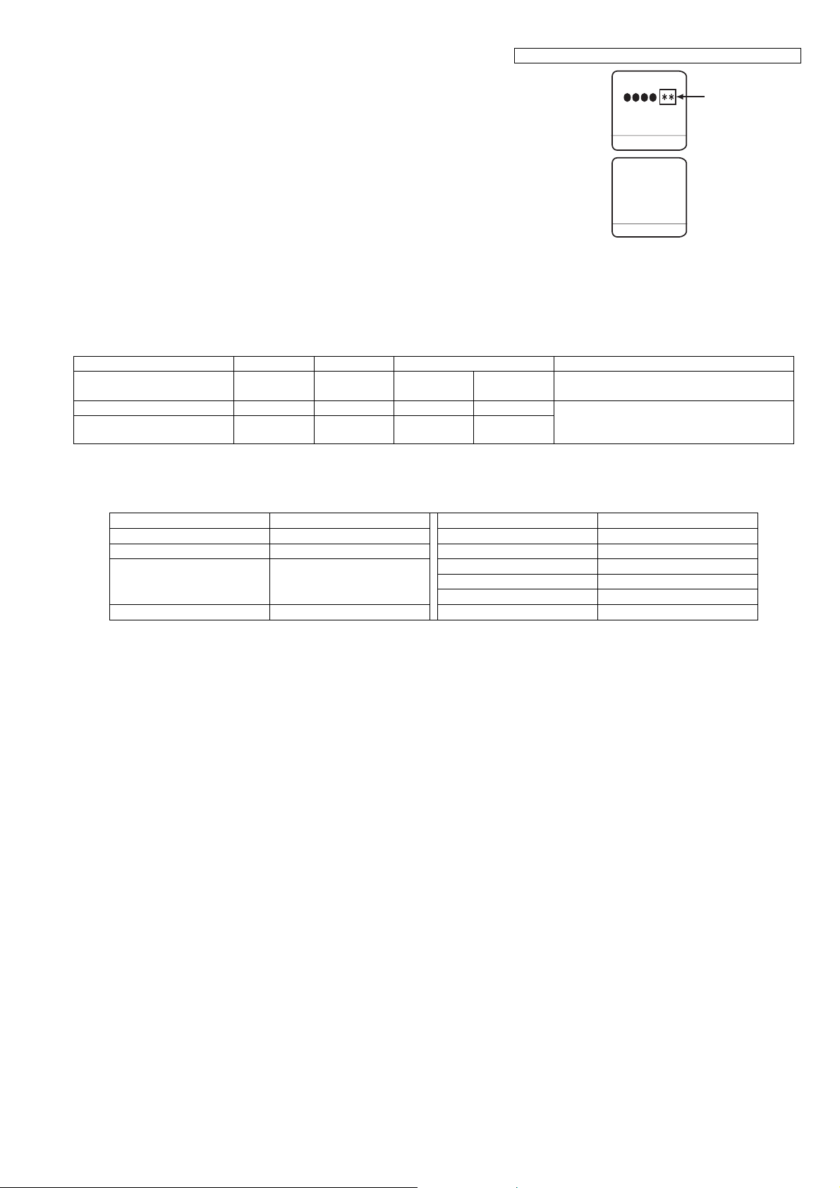
5). Enter "
6). Enter "
ە
", "ە", "ە", "ە" (Address). (*1)
㸨
", "㸨" (New Data). (*1)
26
BACK
Set Addr.:
CLEAR
SELECT
Default Data
OK
KX-TGE210/KX-TGE212/KX-TGE232/KX-TGE233/KX-TGE234/TGEA20
7). Press {OK} , a long confirmation beep
will be heard.
8).
Press to return to standby mode.
After that, turn the base unit power off and then power on.
Note:
New Data
_ _ _ _ _ _
Set Addr.:
Set Addr.:
{OFF}
CLEAR
OK
BACK
* "Set tel line" isn't displayed in Cell line only mode.
To return to normal mode, execute the following procedure:
1 {MENU} i {#}{1}{5}{7}
2 {V}/{^}: Select "off "i {SELECT}
3 {OFF}
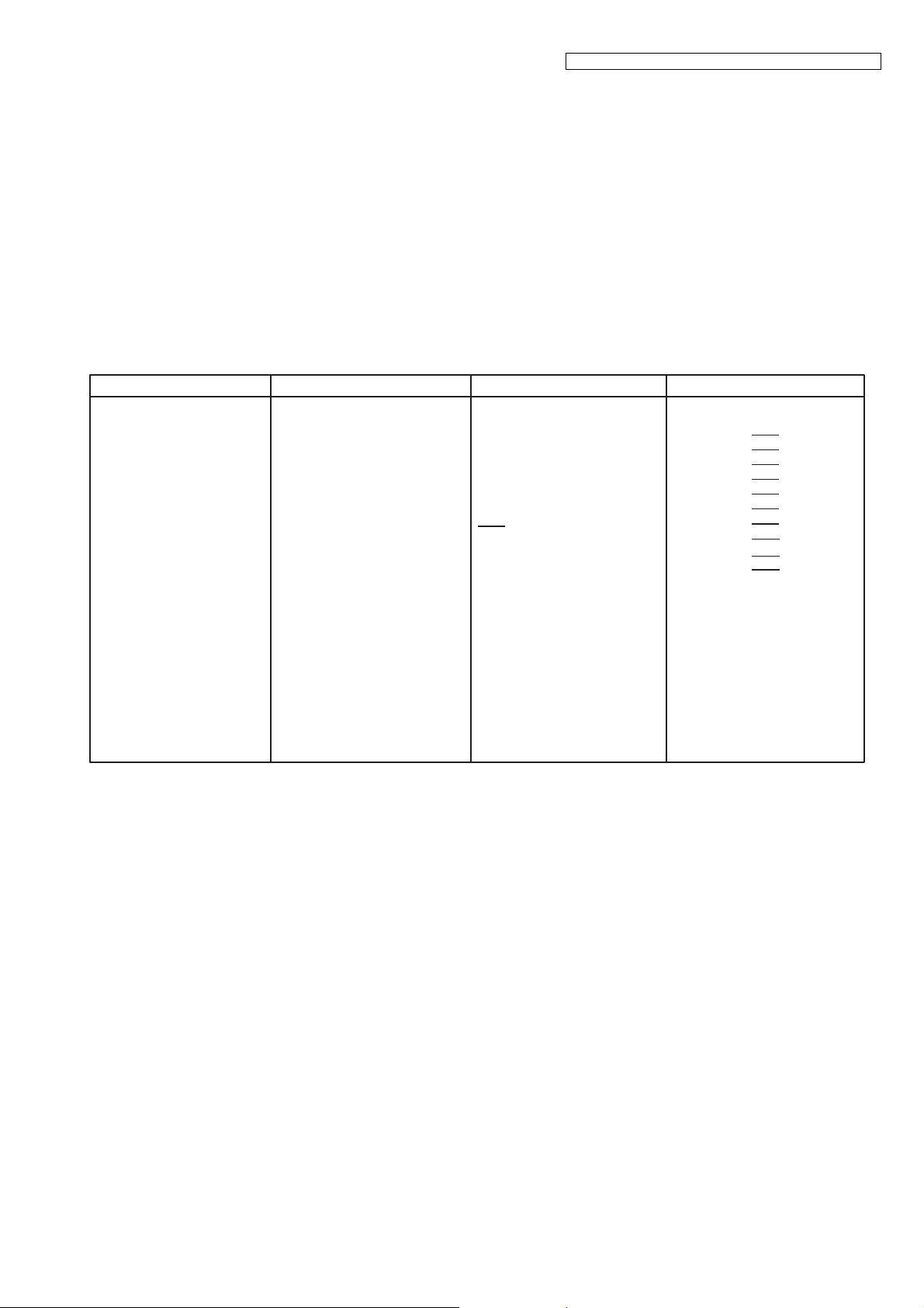
Frequently Used Items (Base Unit)
ex.)
Items Address Default Data New Data Remarks
C-ID (FSK) sensitivity 06 0B 00 01 (6dB UP) 02 (12dB UP) When hex changes from"00" to "01" or "02"
gain increases by 6dB or 12dB.
Frequency 00 07 / 00 08 70/02 - - Use these items in a READ-ONLY mode to
ID 00 02 ~ 00 06 Given value - -
confirm the contents. Careless rewriting may
cause serious damage to the computer system.
Note:
(*1) When you enter the address or New Data, please refer to the table below.
Desired Number (hex) Input Keys Desired Number (hex) Input Keys
0 0 A [Flash] + 0
1 1 B [Flash] + 1
. . C [Flash] + 2
. . D [Flash] + 3
. . E [Flash] + 4
9 9 F [Flash] + 5
27

KX-TGE210/KX-TGE212/KX-TGE232/KX-TGE233/KX-TGE234/TGEA20
8.1.2. Handset
Important:
Make sure the address on LCD is correct when entering new data. Otherwise, you may ruin the unit.
{OFF}
Dial keypad
{FLASH}
H/S key operation H/S LCD
1). Press {MENU}.
{CALL WAIT}
2). Select "Settings" using or
then press
{SELECT} or {>}.
{^} {V}
3). Enter "7", "2", "6", "2", "7", "6", "6", "4".
Note: 7262 7664 = PANA SONI
(see letters printed on dial keys)
4). Select "Write EEP" using or
then press
5). Enter "
6). Enter "
7). Press
{SELECT} or {>}.
ە
", "ە", "ە", "ە" (Address). (*1)
㸨
", "㸨" (New Data). (*1)
{OK} , a long confirmation beep
{^} {V}
will be heard.
Service Mode
Read EEP
Write EEP
BACK
SELECT
Set Addr.:
CLEAR
Set Addr.:
CLEAR
Set Addr.:
_ _ _ _ _ _
Default Data
OK
New Data
OK
8).
{OFF}
Press to return to standby mode.
BACK
After that, remove and reinsert the batteries. Press the Power button for
about 1 second if the power is not turned on.
28
Frequently Used Items (Handset)
ex.)
KX-TGE210/KX-TGE212/KX-TGE232/KX-TGE233/KX-TGE234/TGEA20
Items Address Default Data New Data Possible Adjusted
Value MA X (hex)
Battery Low 00 12/00 13 00 / 00 - - -
Frequency 00 07 / 00 08 00 / 01 - - -
ID 00 02 ~ 00 06 Given value - - -
Possible Adjusted
Value MIN (hex)
Remarks
(*2)
Note:
(*1) When you enter the address or New Data, please refer to the table below.
Desired Number (hex.) Input Keys Desired Number (hex.) Input Keys
0 0 A [Flash] + 0
1 1 B [Flash] + 1
. . C [Flash] + 2
. . D [Flash] + 3
. . E [Flash] + 4
9 9 F [Flash] + 5
(*2) Use these items in a READ-ONLY mode to confirm the contents. Careless rewriting may cause serious damage to the
handset.
29
 Loading...