

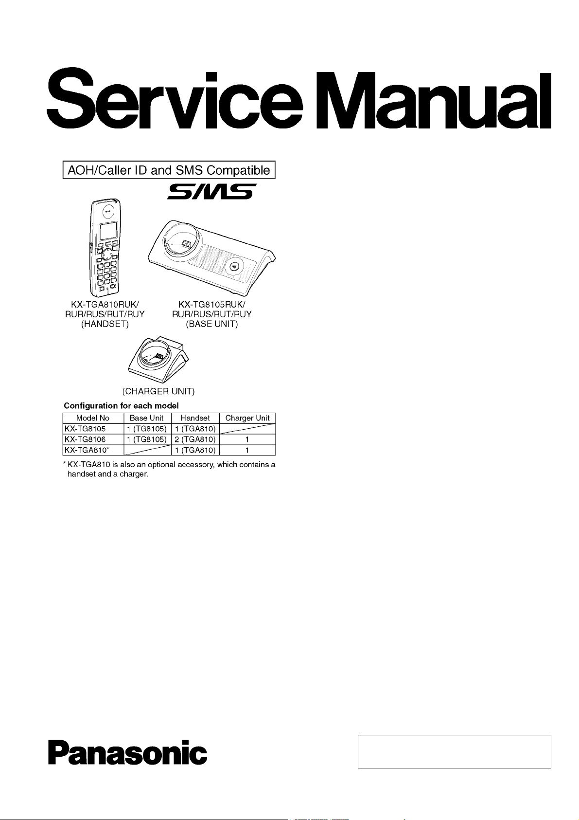
Panasonic KX-TG8106RU, KX-TG8105RU, KX-TGA810RU Service manual
Telephone Equipment
KX-TG8105RU
KX-TG8106RU
KX-TGA810RU
Digital Cordless Phone
RUK - Black Carbon Version
RUR - Red Version
RUS - Silver Version
RUT - Titanium Black Version
RUY - White Carbon Version
(for Russia)
ORDER NO. KM40607157CE
© 2006 Panasonic Communications Co., Ltd. All
rights reserved. Unauthorized copying and
distribution is a violation of law.
KX-TG8105RU/KX-TG8106RU/KX-TGA810RU
2

TABLE OF CONTENTS
PAG E PAG E
1 Safety Precautions ----------------------------------------------- 4
1.1. For Service Technicians --------------------------------- 4
2 Warning-------------------------------------------------------------- 4
2.1. Battery Caution--------------------------------------------- 4
2.2. About Lead Free Solder (Pbf: Pb free)--------------- 4
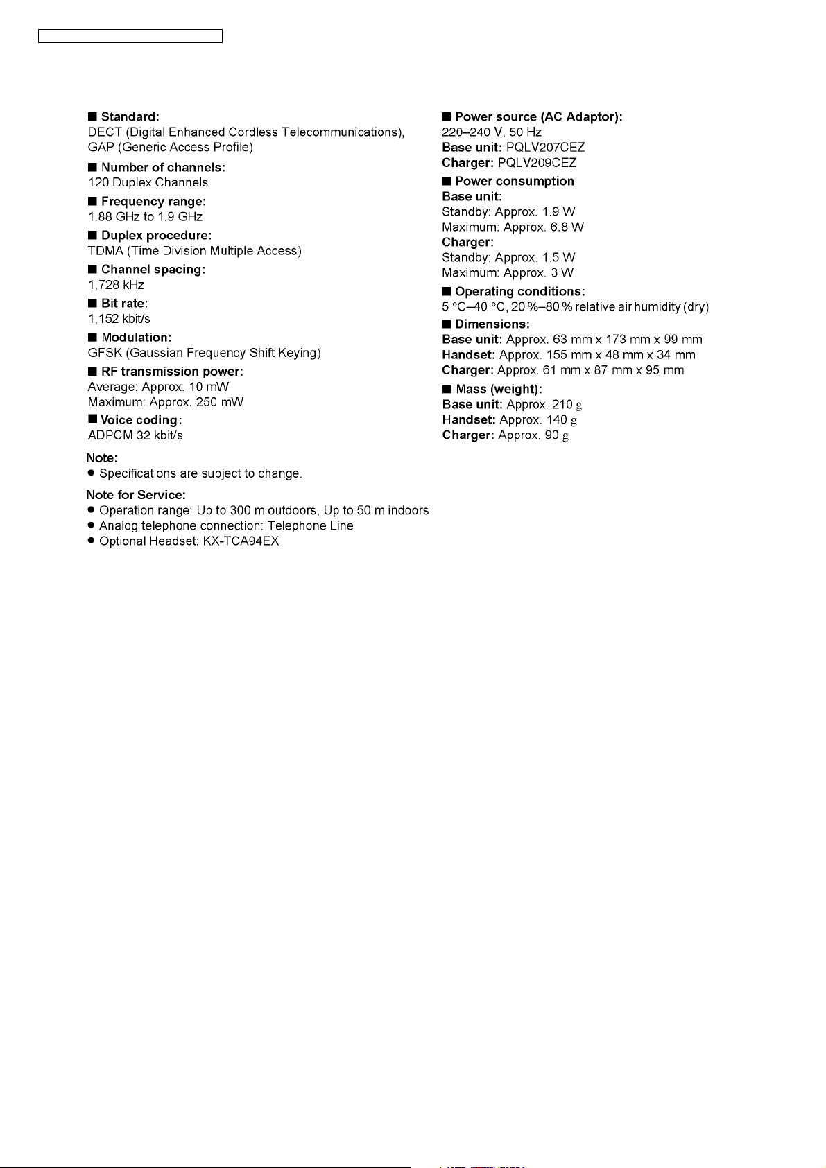
3 Specifications ----------------------------------------------------- 6
4 Technical Descriptions ----------------------------------------- 7
4.1. Block Diagram (Base Unit) ------------------------------ 7
4.2. Circuit Operation (Base Unit) --------------------------- 8
4.3. Block Diagram (Handset)-------------------------------10
4.4. Circuit Operation (Handset)----------------------------11
4.5. Circuit Operation (Charger Unit) ----------------------11
4.6. Signal Route -----------------------------------------------12
5 Location of Controls and Components ------------------13
5.1. Controls -----------------------------------------------------13
6 Installation Instructions ---------------------------------------14
6.1. Connections------------------------------------------------14
6.2. Battery-------------------------------------------------------14
7 Operation Instructions-----------------------------------------16
7.1. Base Unit Settings----------------------------------------16
7.2. Handset Settings -----------------------------------------17
7.3. Registering a Handset to a Base Unit ---------------19
7.4. For Service Hint-------------------------------------------20
8 Service Mode -----------------------------------------------------21
8.1. Engineering Mode ----------------------------------------21
8.2. EEPROM Layout (Base Unit)--------------------------26
8.3. EEPROM Layout (Handset) ---------------------------31
9 Troubleshooting Guide ----------------------------------------34
9.1. Troubleshooting Flowchart -----------------------------34
9.2. Troubleshooting by Symptom (Base Unit and
Charger Unit) ----------------------------------------------42
9.3. Troubleshooting by Symptom (Handset) -----------46
9.4. How to Replace the Flat Package IC ----------------49
10 Disassembly and Assembly Instructions ---------------51
10.1. Disassembly Instructions -------------------------------51
10.2. Assembly Instructions -----------------------------------54
11 Measurements and Adjustments---------------------------55
11.1. The Setting Method of JIG (Base Unit) -------------55
11.2. Adjustment Standard (Base Unit)---------------------57
11.3. Adjustment Standard (Charger Unit)-----------------58
11.4. The Setting Method of JIG (Handset) ---------------59
11.5. Adjustment Standard (Handset) ----------------------61
11.6. Things to Do after Replacing IC ----------------------62
11.7. RF Specification-------------------------------------------63
11.8. How to Check the Handset Speaker or
Receiver ----------------------------------------------------64
11.9. Frequency Table (MHz) ---------------------------------64
12 Schematic Diagram ---------------------------------------------65
12.1. For Schematic Diagram---------------------------------65
12.2. Schematic Diagram (Base Unit) ----------------------66
12.3. Schematic Diagram (Handset) ------------------------68
12.4. Schematic Diagram (Charger Unit) ------------------70
13 Printed Circuit Board-------------------------------------------71
13.1. Circuit Board (Base Unit) -------------------------------71
13.2. Circuit Board (Handset) ---------------------------------73
13.3. Circuit Board (Charger Unit) ---------------------------75
14 Appendix Information of Schematic Diagram ---------76
14.1. CPU Data (Base Unit) -----------------------------------76
KX-TG8105RU/KX-TG8106RU/KX-TGA810RU
14.2. CPU Data (Handset) ------------------------------------ 78
14.3. Terminal Guide of the ICs, Transistors and
Diodes ------------------------------------------------------ 80
15 Exploded View and Replacement Parts List ----------- 81
15.1. Cabinet and Electrical Parts (Base Unit) ----------- 81
15.2. Cabinet and Electrical Parts (Handset)------------- 82
15.3. Cabinet and Electrical Parts (Charger Unit) ------- 83
15.4. Accessories and Packing Materials ----------------- 84
15.5. Replacement Parts List--------------------------------- 87
3
KX-TG8105RU/KX-TG8106RU/KX-TGA810RU
1 Safety Precautions
1.1. For Service Technicians
ICs and LSIs are vulnerable to static electricity.
When repairing, the following precautions will help prevent recurring malfunctions.
1. Cover plastic parts boxes with aluminum foil.
2. Ground the soldering irons.
3. Use a conductive mat on worktable.
4. Do not grasp IC or LSI pins with bare fingers.
2Warning
2.1. Battery Caution
1. Danger of explosion if battery is incorrectly replaced.
2. Replace only with the same or equivalent type recommended by the manufacturer.
3. Dispose of used batteries according to the manufacturer's Instructions.
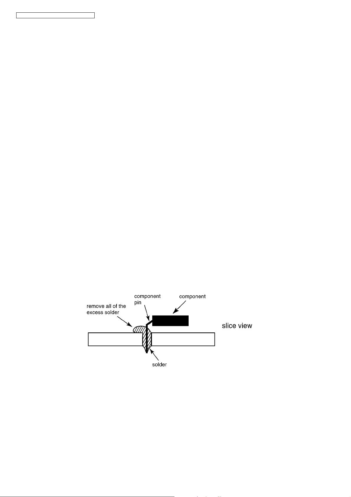
2.2. About Lead Free Solder (Pbf: Pb free)
Note:
In the information below, Pb, the symbol for lead in the periodic table of elements, will refer to standard solder or solder that contains lead.
We will use PbF solder when discussing the lead free solder used in our manufacturing process which is made from Tin (Sn),
Silver (Ag), and Copper (Cu).
This model, and others like it, manufactured using lead free solder will have PbF stamped on the PCB. For service and repair
work we suggest using the same type of solder.
Caution
• PbF solder has a melting point that is 50°F ~ 70° F (30°C ~ 40°C) higher than Pb solder. Please use a soldering iron with temperature control and adjust it to 700°F ± 20° F (370°C ± 10°C).
• Exercise care while using higher temperature soldering irons.:
Do not heat the PCB for too long time in order to prevent solder splash or damage to the PCB.
• PbF solder will tend to splash if it is heated much higher than its melting point, approximately 1100°F (600°C).
• When applying PbF solder to double layered boards, please check the component side for excess which may flow onto the
opposite side (See the figure below).
4
KX-TG8105RU/KX-TG8106RU/KX-TGA810RU
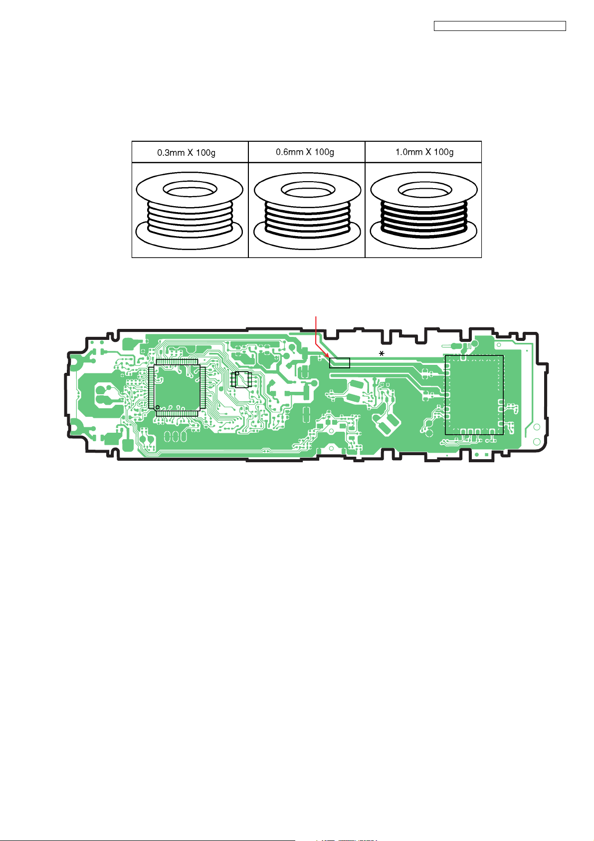
2.2.1. Suggested PbF Solder
There are several types of PbF solder available commercially. While this product is manufactured using Tin, Silver, and Copper
(Sn+Ag+Cu), you can also use Tin and Copper (Sn+Cu), or Tin, Zinc, and Bismuth (Sn+Zn+Bi). Please check the manufacturer’s specific instructions for the melting points of their products and any precautions for using their product with other materials.
The following lead free (PbF) solder wire sizes are recommended for service of this product: 0.3 mm, 0.6 mm and 1.0 mm.
2.2.2. How to Recognize that Pb Free Solder is Used
(Example: Handset P.C.B.)
Marked
60
80
1
IC1
41
4061
21
20
148
IC3
5
(Component View)
Note:
The location of the “PbF” mark is subject to change without notice.
KX-TG8120/TG8100/TGA810
PQUP11411Z
PbF
32
110
11
27
IC4
16
26
17
5
KX-TG8105RU/KX-TG8106RU/KX-TGA810RU
3 Specifications
6
4 Technical Descriptions
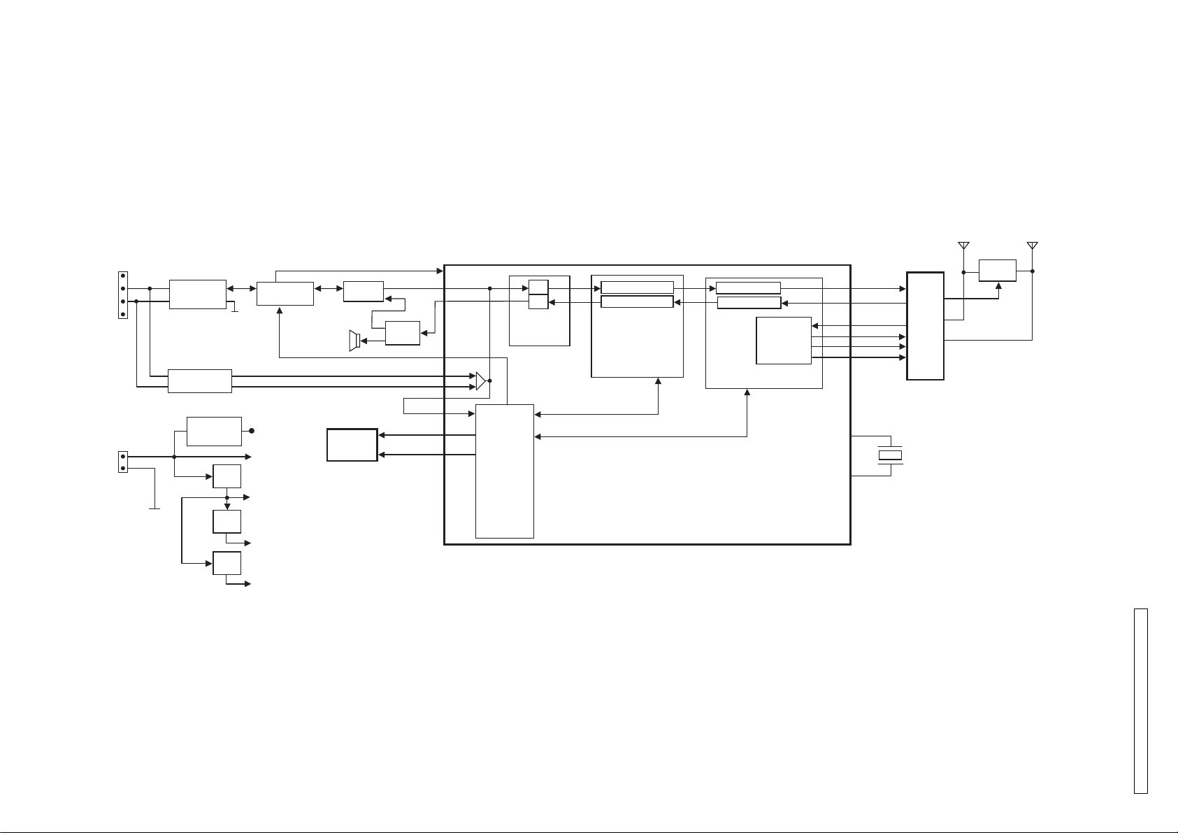
D3
4.1. Block Diagram (Base Unit)
To TEL_LINE
CN1
A
B
7
To AC Adaptor
CN2
Bridge
Rect D3
Bell/Caller ID
Interface
Limit
Resistor
3.3V
Reg.
2.5V
Reg.
1.8V
Reg.
Hook Switch
CHARGE
CONTACT
VUNREG
IC1
3.3V
Q9
2.5V
Q8
1.8V
Off-Hook Line Voltage
Q4,Q5
HOOK
Audio
EEPROM
IC5
Analog
Switch
SCL
SDA
BELL
64 ADCO
59
54
61
52
60
56
55
6
5
CPU
D/A
A/D
Analog
Front
End
Speech Decoding
Speech Encoding
ADPCM
Codec Filter
DSP
BBIC
IC7
Burst Decoding
Burst Encoding
Interface
BMC
RF
ANT1
TXDA
18
19
15
RSSI
20
SYCL
21
SYDA
22
SYEN
12
13
RXDA
XTAL
X1
18
31
16
2
8
14
21
13
12
IC10
RF Module
10.368
MHz
ANT2
KX-TG8105/8106 BLOCK DIAGRAM (BASE UNIT)
KX-TG8105RU/KX-TG8106RU/KX-TGA810RU
KX-TG8105RU/KX-TG8106RU/KX-TGA810RU
4.2. Circuit Operation (Base Unit)
4.2.1. Outline
Base Unit consists of the following ICs as shown in Block Diagram (Base Unit) (P.7).
• DECT BBIC (Base Band IC): IC7
- Handling all the audio, signal and data processing needed in a DECT base unit
- Controlling the DECT specific physical layer and radio section (Burst Module Controller section)
- ADPCM code filter for speech encoding and speech decoding (DSP section)
- Echo-cancellation and Echo-suppression (DSP section)
- Any tones (tone, sidetone, ringing tone, etc.) generation (DSP section)
- DTMF receiver (DSP section)
- Clock Generation for RF Module
- ADC, DAC, timer, and power control circuitry
- All interfaces (ex: RF module, EEPROM, LED, Analog Front End, etc.)
• RF Module: IC10
- PLL Oscillator
- Detector
- Compress/Expander
- First Mixer
- Amplifier for transmission and reception
• EEPROM: IC5
- Temporary operating parameters (for RF, etc.)
• Additionally,
- Power Supply Circuit (+3.3V, +2.5V, +1.8V output)
- Crystal Circuit (10.368MHz)
- Charge Circuit
- Telephone Line Interface Circuit
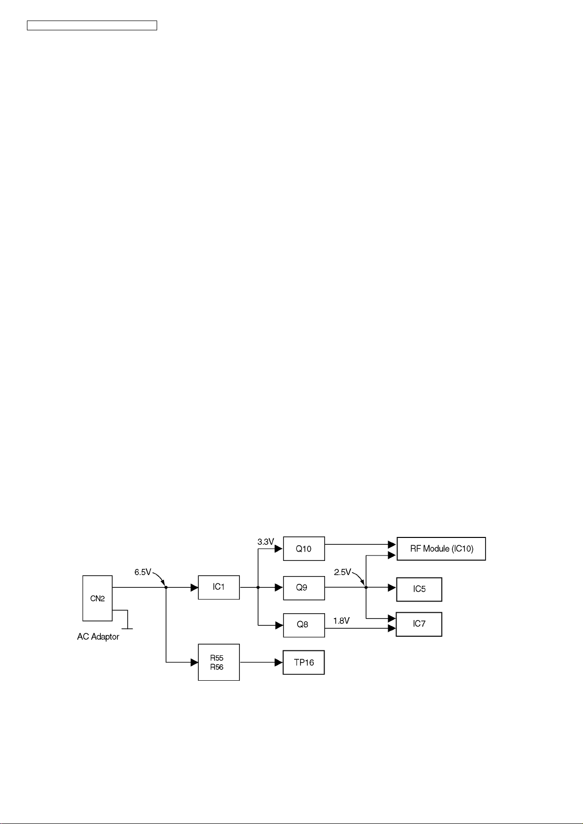
4.2.2. Power Supply Circuit
The power is supplied to the DECT BBIC, RF Module, EEPROM and Charge Contact from AC Adaptor (+6.5V) as shown in
Fig.101. The power supply is as follows;
• DECT BBIC (IC7):
CN2 (+6.5V) → IC1 → Q9 → IC7
CN2 (+6.5V) → IC1 → Q8 → IC7
• RF Module (IC10):
CN2 (+6.5V) → IC1 → Q9 → IC10 (PLL)
CN2 (+6.5V) → IC1 → Q10 → IC10 (Power AMP)
• EEPROM (IC5):
CN2 (+6.5V) → IC1 → Q9 → IC5
• Charge Contact (TP16):
CN2 (+6.5V) → R55, R56 → TP16
<Fig.101>
8

KX-TG8105RU/KX-TG8106RU/KX-TGA810RU
4.2.3. Telephone Line Interface
<Function>
• Bell signal detection
• Clip signal detection
• ON/OFF hook circuit
Bell & Clip (: Calling Line Identification Presentation: Caller ID) signal detection:
In the standby mode, Q3 is open to cut the DC loop current and decrease the ring load.
When ring voltage appears at the L1T (A) and L1R (B) leads (when the telephone rings), the AC ring voltage is transferred as
follows;
•A → C4 → R6 → R33 → IC7 Pin 60 (CID INp)
•B → C3 → R4 → R35 → IC7 Pin 52 (CID INn)
ON/OFF hook circuit:
In the standby mode, Q3 is open, and connected as to cut the DC loop current and to cut the voice signal. The unit is consequently in an on-hook condition.
When IC7 detects a ring signal or press the TALK Key onto the handset, Q4 turns on and then Q3 turns on, thus providing an
off-hook condition (DC current flows through the circuit) and the following signal flow makes the loop current.
•A → D3 → Q3 → Q5 → R21 → R22 → D3 → B [OFF HOOK]
4.2.4. Transmitter/Receiver
• Audio Circuits and DTMF tone signal circuits.
Base Unit and Handset mainly consist of RF Module and DECT BBIC.
Base Unit and Handset transmit/receive voice signal and data signal through the antenna on carrier frequency.
Signal Path:
*Refer to Signal Route (P.12).
4.2.4.1. Transmitter Block
The voice signal input from the TEL LINE interface goes to RF Module (IC10) through DECT BBIC (IC7) as shown in Block Diagram (Base Unit) (P.7)
The voice signal passes through the analog part of IC7 where it is amplified and converted to a digital audio stream signal. The
burst switch controller processes this stream performing encryption and scrambling, adding the various other fields to produce
the GAP (Generic Access Profile) standard DECT frame, assigning to a time slot and channel etc.
In IC10, the carrier frequency is changing, and frequency modulated RF signal is generated and amplified, and radiated from
antenna. Handset detects the voice signal or data signal in the circuit same as the following explanation of Receiver Block.
4.2.4.2. Receiver Block
The signal of 1900 MHz band (1881.792 MHz ~ 1897.344 MHz) which is input from antenna is input to IC10 as shown in Block
Diagram (Base Unit) (P.7).
In IC10, the signal of 1900 MHz band is downconverted to 864 kHz signal and demodulated, and goes to IC7 as GAP (Generic
Access Profile) standard DECT frames. It passes through the decoding section burst switch controller where it separates out the
frame information and performs de-encryption and de-scrambling as required. It then goes to the DSP section where it is turned
back into analog audio. This is amplified by the analog front end, and goes to the TEL LINE Interface.
4.2.5. Pulse Dialling
During pulse dialing the hookswitch (Q3, Q4) is used to generate the pulses using the HOOK control signal, which is set high
during pulses. To force the line impedance low during the “pause” intervals between dial pulses, the PULSE_DIAL signal turns
on Q2.
9
KX-TG8105RU/KX-TG8106RU/KX-TGA810RU
Q1
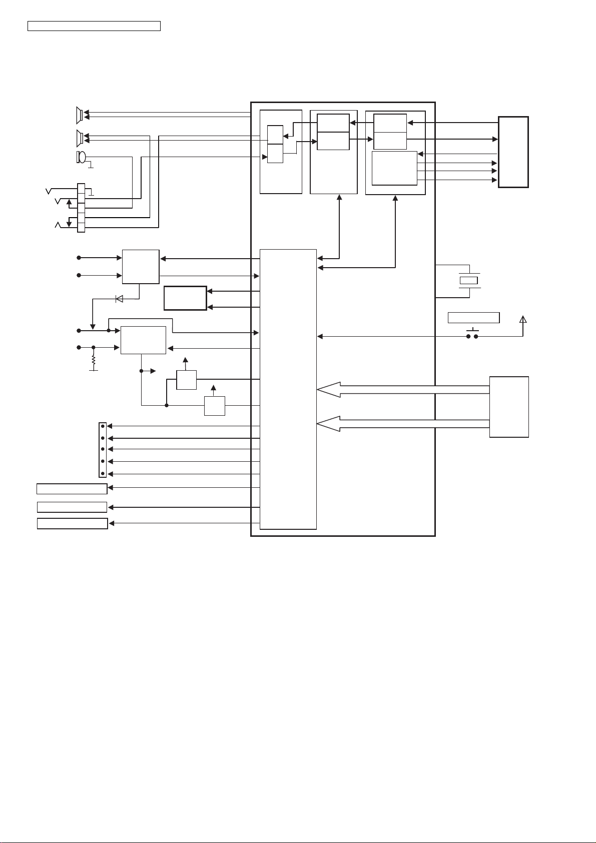
4.3. Block Diagram (Handset)
SPEAKER
RECEIVER
MIC
CN4
1
2
3
4
5
Headset
CHARGE(+)
CHARGE
CONTACTS
CHARGE(-)
J1
BATTERY
TERMINAL
J2
LCD
LCD-BACK LIGHT
KEY-BACK LIGHT
Ringer LED
CHARGE
CIRCUIT
Q4,Q5,Q9
R7
D7
SWITCHED
SUPPLY
Q1
CHARGE
CHARGE DETECT
EEPROM
IC3
DC/DC-SWITCH
4.0V
2.5V
2.5V
Q3
RESET
CSB
SDA
SCL
VBAT1
1.8V
Q2
CD
SCL
SDA
1.8V
30
32
66
67
72
62
52
45
44
58
56
59
60
11
77
47
46
75
RXDA
23
22
19
25
26
24
TXDA
RSSI
SYDA
SYEN
SYCL
RF
Module
IC4
D/A
A/D
Analog
Front
End
Speech
Decoding
Speech
Encoding
ADPCM
Codec
Filter
DSP
Burst
Decoding
Burst
Encoding
RF
Interface
BMC
XTAL
16
X1
10.368
17
ON SWITCH
MHz
BATTERY
61
CPU
1,12,40,76
27,28,34,35,36,74
ROWS
COLUMNS
KEYPAD
6
5
BBIC
IC1
9
KX-TGA810 BLOCK DIAGRAM (HANDSET)
10
KX-TG8105RU/KX-TG8106RU/KX-TGA810RU
4.4. Circuit Operation (Handset)
4.4.1. Outline
Handset consists of the following ICs as shown in Block Diagram (Handset) (P.10).
• DECT BBIC (Base Band IC): IC1
- All data signals (forming/analyzing ACK or CMD signal)
- All interfaces (ex: Key, Detector Circuit, Charge, DC/DC Converter, EEPROM, LCD)
•RF Module: IC4
- PLL Oscillator
- Detector
- Compress/Expander
- Amplifier for transmission and reception
• EEPROM: IC3
- Temporary operating parameters (for RF, etc.)
4.4.2. Power Supply Circuit/Reset Circuit
Circuit Operation:
When power on the Handset, the voltage is as follows;
BATTERY(2.2 V ~ 2.6 V: J1) → F1, L1, D1 → Q2 (1.8 V), Q3 (2.5 V), Q1 (4.2 V)
The Reset signal generates IC1 (53 pin) and 1.8 V.
4.4.3. Charge Circuit
Circuit Operation:
When charging the handset on the Base Unit, the charge current is as follows;
DC+(6.5V) → R55, R56 → CHARGE+(Base) → CHARGE+(Handset) → L4 → Q4 → D7→ F1 → BATTERY+ ... Battery ...
BATTERY- → R45 → GND → CHARGE-(Handset)→ CHARGE-(Base) → GND → DC-(GND)
In this way, the BBIC on Handset detects the fact that the battery is charged.
The charge current is controlled by switching Q5 of Handset.
Refer to Fig.101 in Power Supply Circuit (P.8).
4.4.4. Battery Low/Power Down Detector
Circuit Operation:
“Battery Low” and “Power Down” are detected by BBIC which check the voltage from battery.
The detected voltage is as follows;
• Battery Low
Battery voltage: V (Batt) 2.25V ± 50mV
The BBIC detects this level and “ ” starts flashing.
• Power Down
Battery voltage: V (Batt) 2.00V ~ 2.05V
The BBIC detects this level and power down.
4.4.5. Speakerphone
The hands-free loudspeaker at SP+ and SP- works as a ringer/alarm as well.
4.5. Circuit Operation (Charger Unit)
4.5.1. Power Supply Circuit
The power supply is as shown.
11
KX-TG8105RU/KX-TG8106RU/KX-TGA810RU
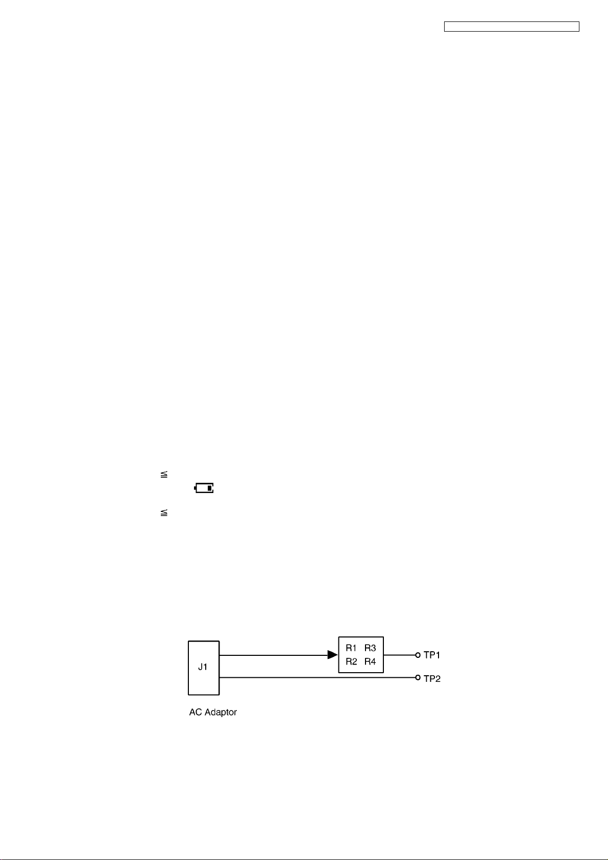
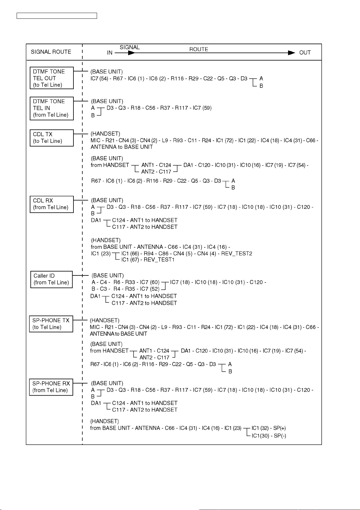
4.6. Signal Route
12
5 Location of Controls and Components
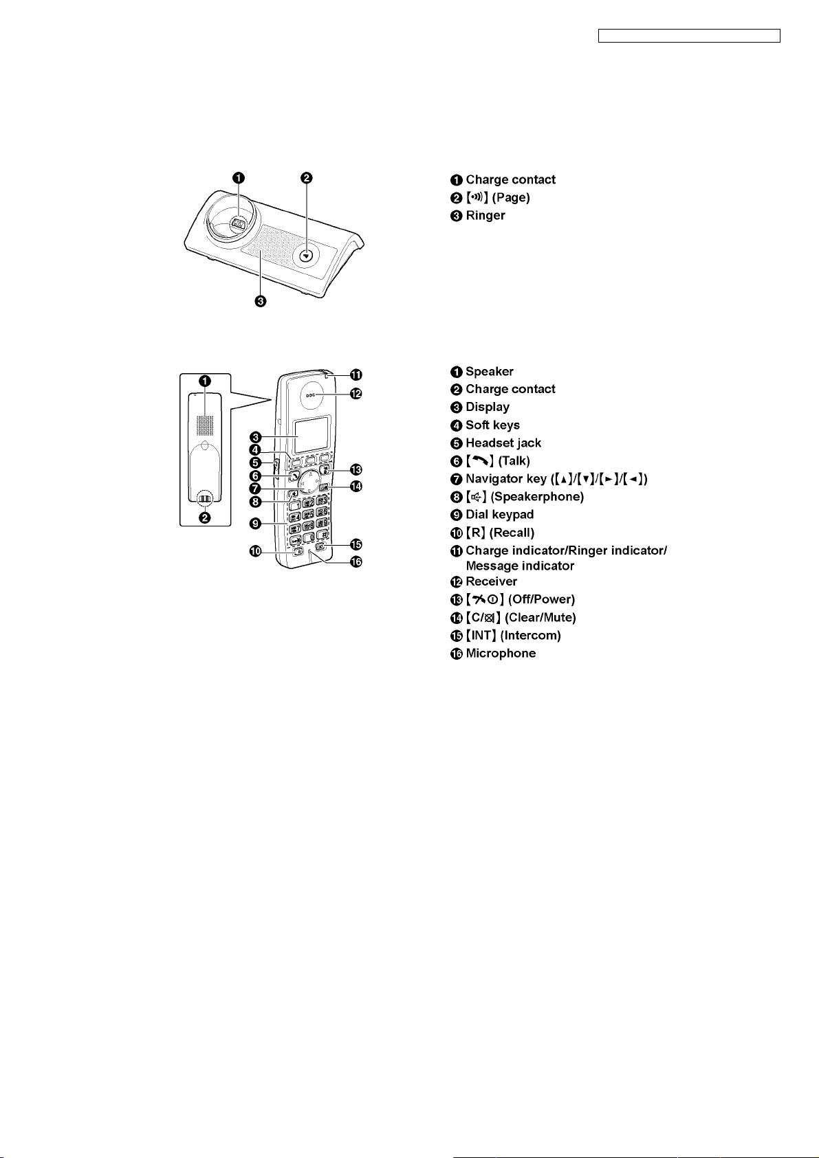
5.1. Controls
5.1.1. Base Unit
5.1.2. Handset
KX-TG8105RU/KX-TG8106RU/KX-TGA810RU
13
KX-TG8105RU/KX-TG8106RU/KX-TGA810RU
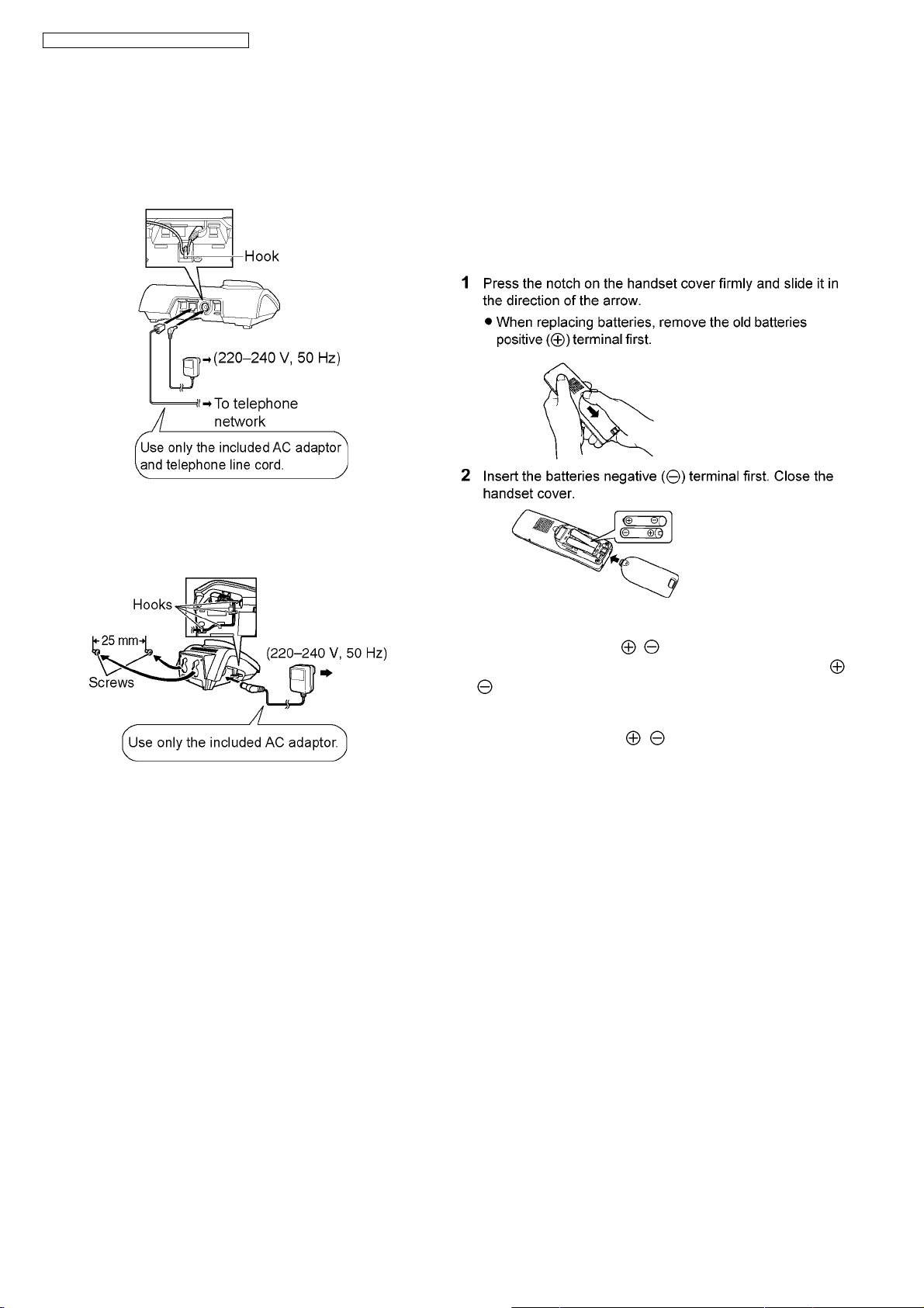
6 Installation Instructions
6.1. Connections
Base unit
When connecting the AC adaptor to the base unit, a short
beep will be heard. If it is not heard, check the connections.
Charger
Connect the AC adaptor to the charger and route the cable
as shown. The charger can be mounted on the wall, if
required.
6.2. Battery
6.2.1. Installation/Replacement
Important:
• Use only the included rechargeable batteries HHR-55AAAB
or HHR-4EPT.
• When replacing batteries, we recommend using the
Panasonic rechargeable batteries P03P.
Note:
• Never install telephone wiring during a lightning storm.
• The AC adaptor must remain connected at all times. (It is
normal for the adaptor to feel warm during use.)
• The AC adaptor should be connected to a vertically oriented
or floor-mounted AC outlet. Do not connect the AC adaptor
to a ceiling-mounted AC outlet, as the weight of the adaptor
may cause it to become disconnected.
Location
• For maximum distance and noise-free operation, place your
base unit:
- away from electrical appliances such as TVs, radios, personal computers or other phones.
- in a convenient, high and central location.
Notice:
When inserting the batteries:
• Wipe the battery ends ( , ) with a dry cloth.
• Install the batteries without touching the battery ends ( ,
) or the unit contacts.
I fully charged the batteries, but the operating time seems
to be short:
• Wipe the battery ends ( , ) and the unit contacts with a
dry cloth.
14
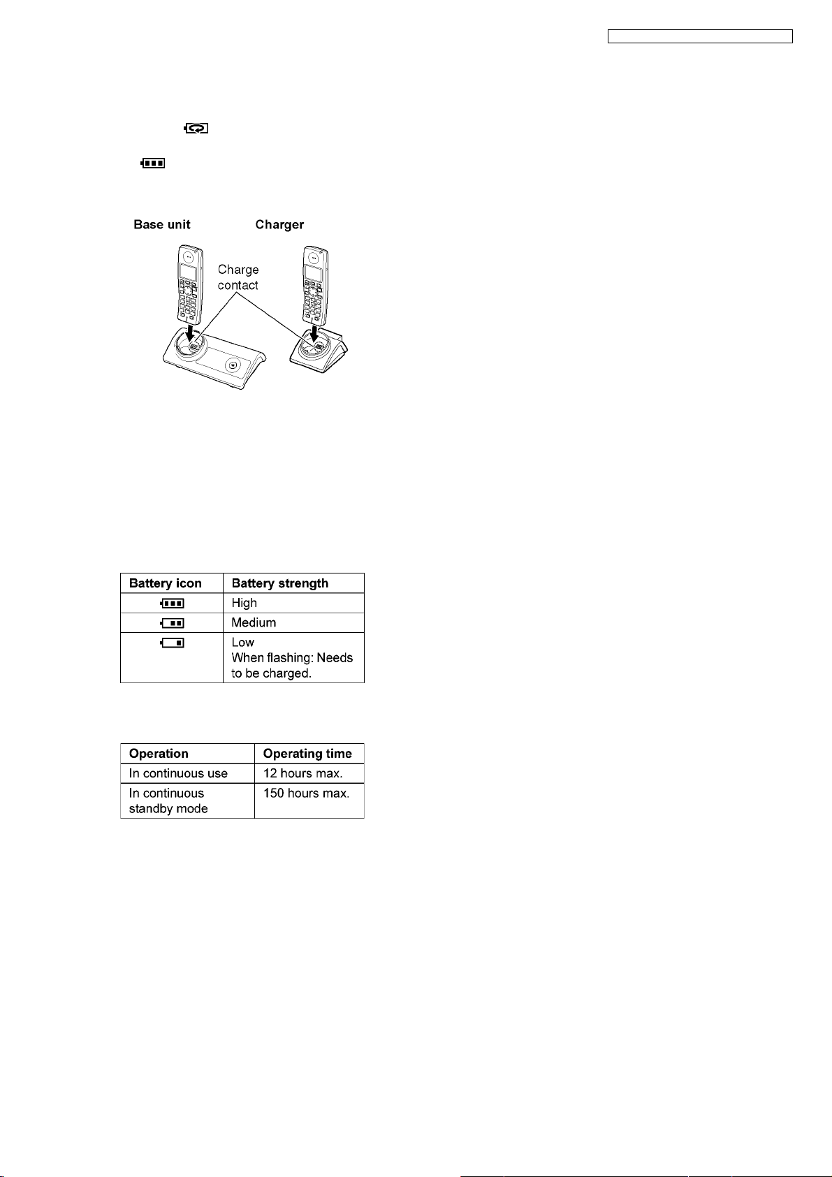
6.2.2. Battery Charge
Place the handset on the base unit or charger for about
7 hours before initial use.
When charging, and battery strength icon are alternately shown on the display. When the batteries are fully
charged, remains on the display.
• The charge indicator lights up when the handset is placed on
the base unit or charger.
Note:
• It is normal for the handset to feel warm during charging.
• If you want to use the unit immediately, charge the batteries
for at least 15 minutes.
• Clean the charge contacts of the handset, base unit, and
charger with a soft, dry cloth, otherwise the batteries may
not charge properly. Clean if the unit is exposed to grease,
dust or high humidity.
KX-TG8105RU/KX-TG8106RU/KX-TGA810RU
6.2.3. Battery Strength
6.2.4. Panasonic Ni-MH Battery Performance (included batteries)
Note:
• It is normal for batteries not to reach full capacity at the initial
charge. Maximum battery performance is reached after a
few complete cycles of charge/discharge (use).
• Actual battery performance depends on a combination of
how often the handset is in use and how often it is not in use
(standby).
• Battery operating time may be shortened over time depending on usage conditions and ambient temperature.
• Even after the handset is fully charged, the handset can be
left on the base unit or charger without any ill effect on the
batteries.
• The battery strength may not be displayed correctly after you
replace the batteries. In this case, place the handset on the
base unit or charger and charge for at least 7 hours.
15
KX-TG8105RU/KX-TG8106RU/KX-TGA810RU
7 Operation Instructions
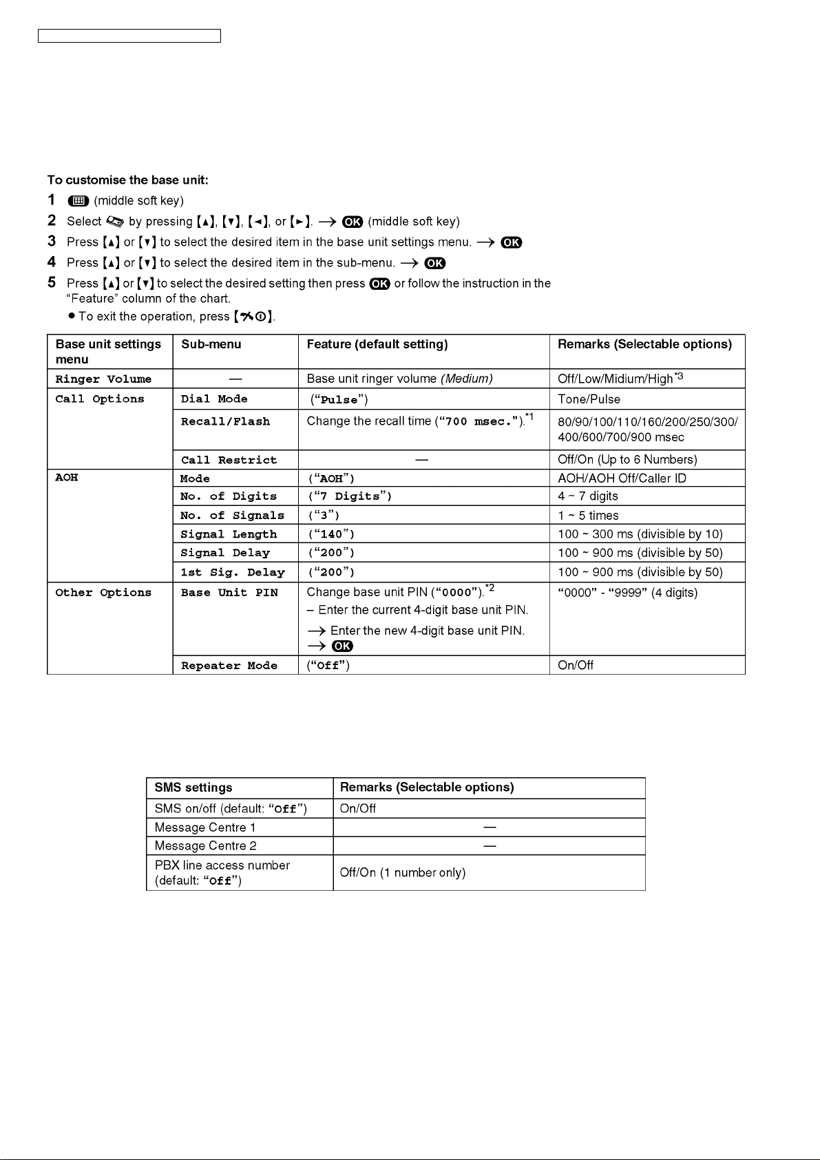
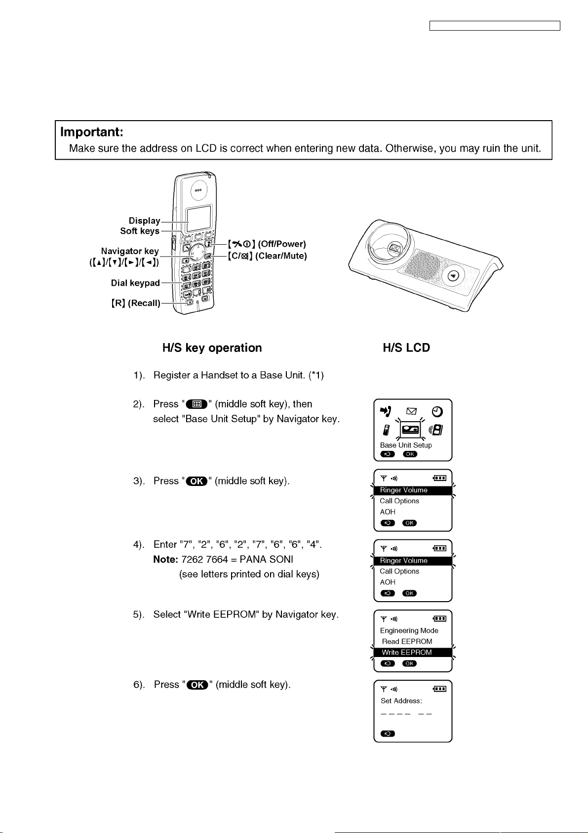
7.1. Base Unit Settings
• Use the handset to customise the base unit.
• When customising the base unit, the current item or setting is highlighted.
*1 Change the recall time, if necessary, depending on the requirements of your service provider/telephone company or PBX.
*2 If you forget your PIN, see For Service Hint (P.20).
*3 The items are not shown on the display.
7.1.1. SMS Settings
16
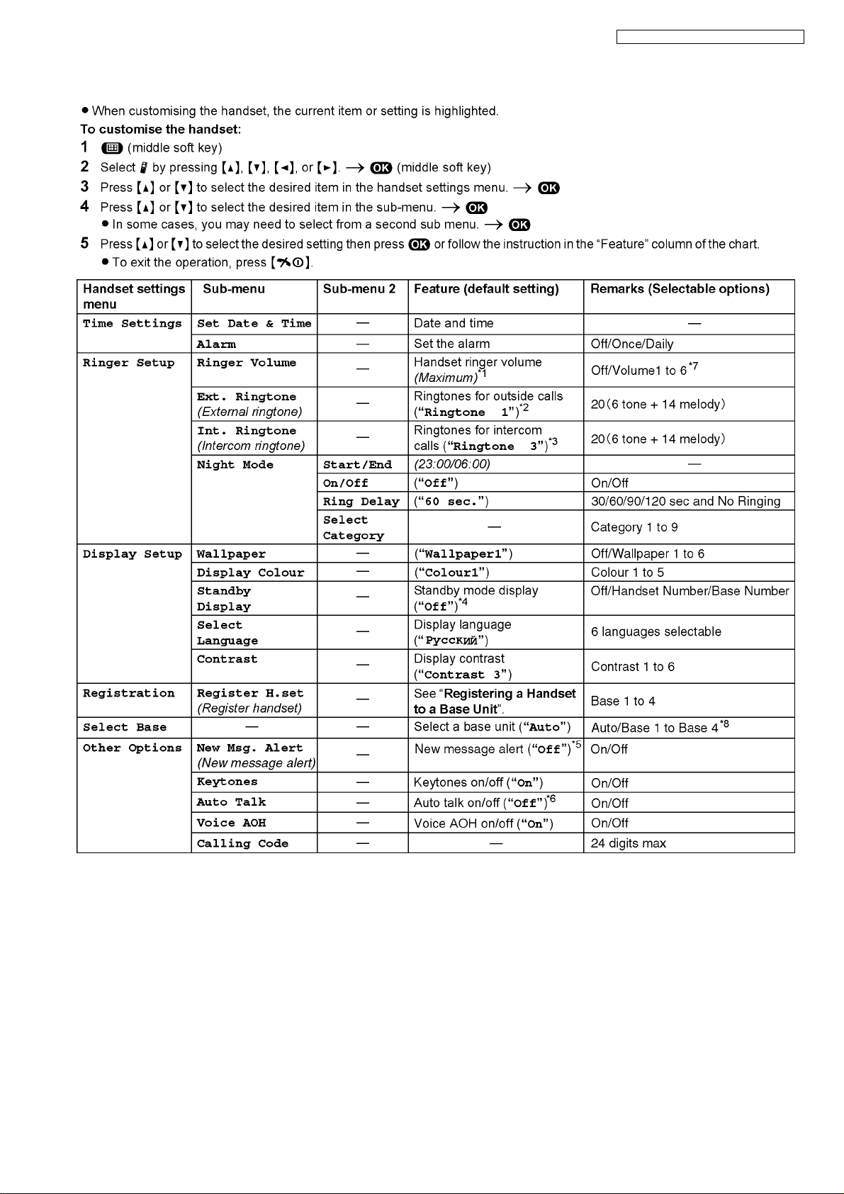
7.2. Handset Settings
KX-TG8105RU/KX-TG8106RU/KX-TGA810RU
17
KX-TG8105RU/KX-TG8106RU/KX-TGA810RU
Cross Reference:
Registering a Handset to a Base Unit (P.19)
18
KX-TG8105RU/KX-TG8106RU/KX-TGA810RU
7.3. Registering a Handset to a Base Unit
The included handset and base unit are preregistered. If for some reason the handset is not registered to the base unit (for
example, flashes even when the handset is near the base unit), register the handset manually.
Cross Reference:
For Service Hint (P.20)
7.3.1. Cancelling a Handset
19
KX-TG8105RU/KX-TG8106RU/KX-TGA810RU
7.3.2. Cancelling a Base Unit
7.4. For Service Hint
20
8 Service Mode
8.1. Engineering Mode
8.1.1. Base Unit
KX-TG8105RU/KX-TG8106RU/KX-TGA810RU
21
KX-TG8105RU/KX-TG8106RU/KX-TGA810RU
Frequently Used Items (Base Unit)
ex.)
Items (*3) Address Default Data New Data Remarks
C-ID (FSK) sensitivity 04 72 00 01 (6dB up) 02 (12dB up) When hex changes from “00” to “01” or “02”, gain
increases by 6dB or 12dB.
C-ID (DTMF) sensitivity 04 80 50 60 (6dB up) 70 (12dB up) When hex changes from “50” to “60” or “70”, gain
increases by 6dB or 12dB.
SMS (FSK) receiving
sensitivity
SMS (FSK) sending
level
Frequency 00 01 75 - - Use these items in a READ-ONLY mode to con-
ID 00 10~00 14 Given value - -
Bell length 01 F6 32 (5sec) (*4) 1E (3sec) 14 (2sec) This is time until bell stops ringing. (Unit: 100ms)
PULSE Dial speed
(10PPS -> 20PPS)
04 72 00 01 (6dB up) 02 (12dB up) When hex changes from “00” to “01” or “02”, gain
increases by 6dB or 12dB.
04 8C/04 8B 0F/B0 19/20 (6dB up) 32/40 (12dB up) When hex changes from “00 0B” to “00 16” or “00
2C”, gain increases by 6dB or 12dB.
firm the contents. Careless rewriting may cause
serious damage to the computer system.
03 5F 28 (40msec) (*4) 14 (20msec) - This is pulse make time. (Unit:1ms)
03 60 3C (60msec) (*4) 1E (30msec) - This is pulse break time. (Unit:1ms)
01 E4 57 (870msec) (*4) 2C (440msec) - This is inter-digit time in pulse mode. (Unit:10ms)
Note:
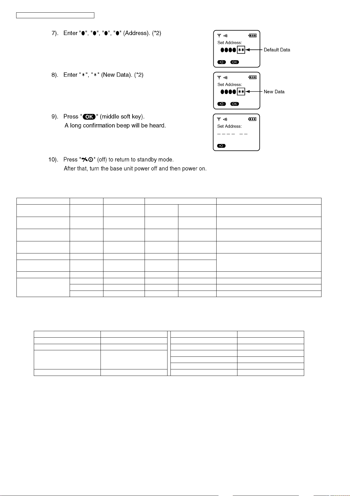
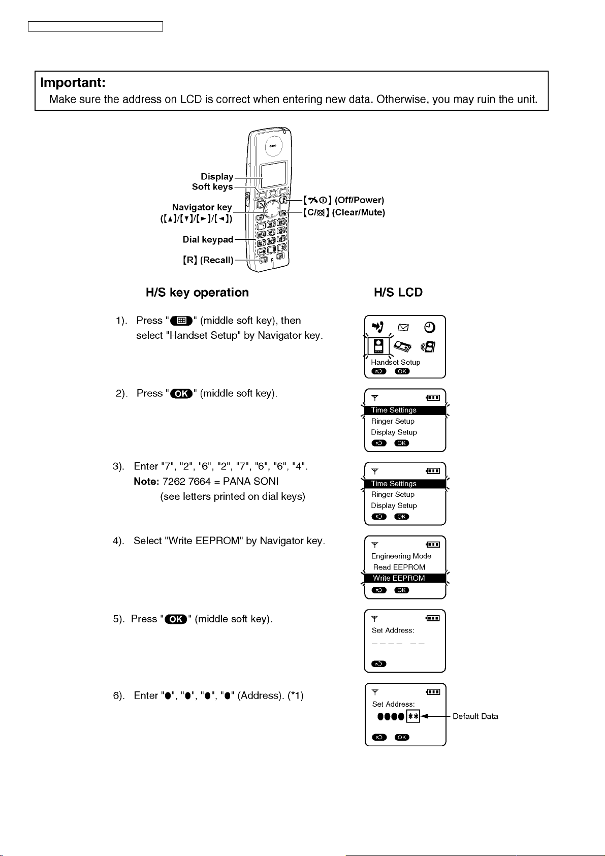
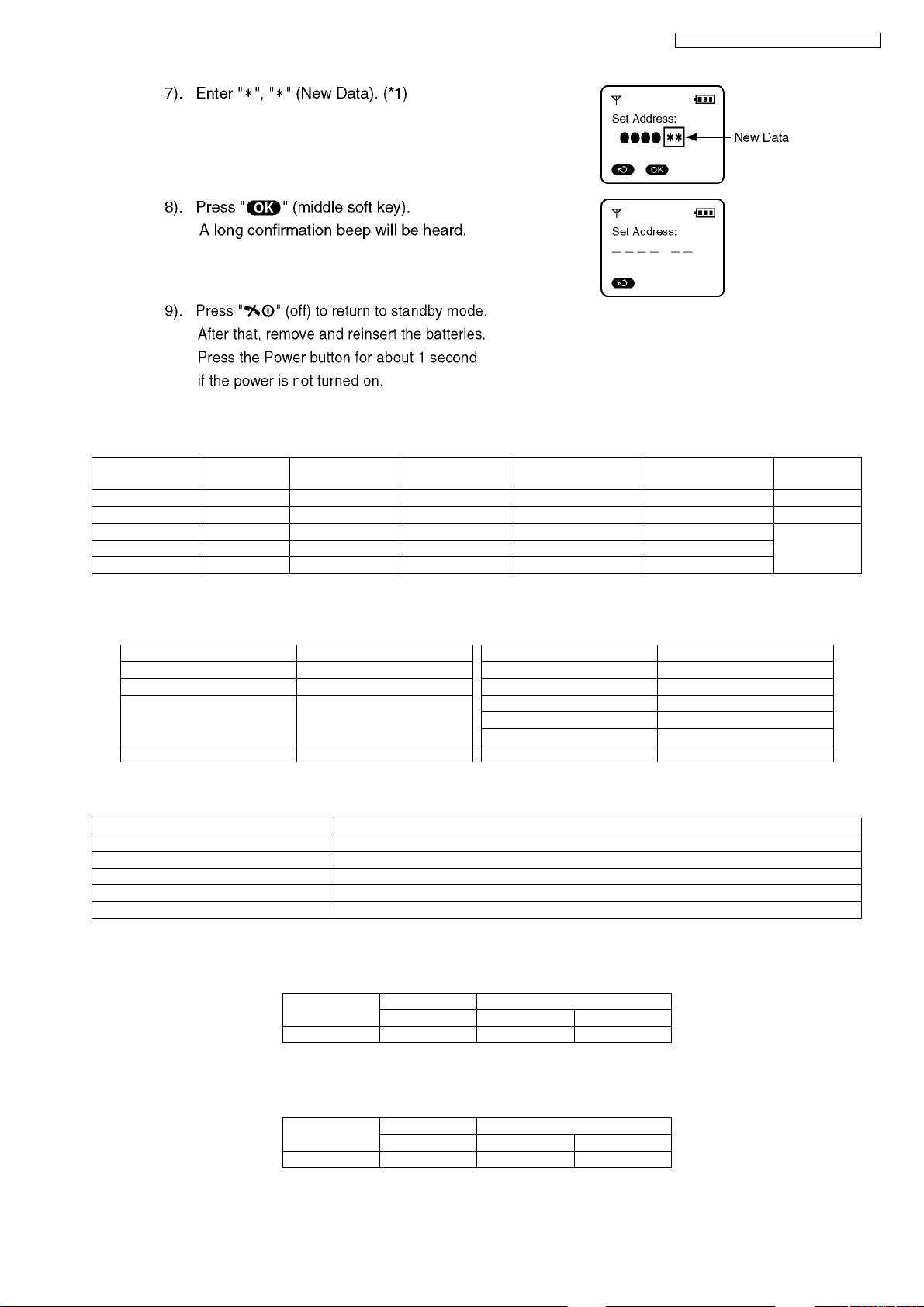
(*1) Refer to Registering a Handset to a Base Unit (P.19).
(*2) When you enter the address or New Data, please refer to the table below.
Desired Number (hex.) Input Keys Desired Number (hex.) Input Keys
00 A[R] + 0
11 B[R] + 1
.. C[R] + 2
.. D[R] + 3
.. E[R] + 4
99 F[R] + 5
22

(*3)
Items Description
C-ID (FSK) sensitivity FSKGain_shiftgain
C-ID (DTMF) sensitivity Foutgains:HPFilter Foutgains
SMS (FSK) receiving sensitivity FSKGain_shiftgain
SMS (FSK) sending level wFskAttn:Signal Output Attenuation (DSP parameter)
Frequency Setting value of FREQ_TRIM_REG
ID ID
Bell length Time until it stops bell.
PULSE Dial speed
(10PPS -> 20PPS)
Pulse MakeTime and BreakTime.
bMakeTime:Pulse MakeTime Unit: 1ms
bBreakTime:Pulse Break Time Unit: 1ms
Inter-digit time in Pulse mode.
Unit:10ms
(*4)
Bell length 32 (hex) = 50 (dec) → 50 × 100msec = 5000msec (5sec)
PULSE Dial speed
(10PPS -> 20PPS)
28 (hex) = 40 (dec) → 40 × 1msec = 40msec
3C (hex) = 60 (dec) → 60 × 1msec = 60msec
57 (hex) = 87 (dec) → 87 × 10msec = 870msec
KX-TG8105RU/KX-TG8106RU/KX-TGA810RU
23
KX-TG8105RU/KX-TG8106RU/KX-TGA810RU
8.1.2. Handset
24
Frequently Used Items (Handset)
ex.)
KX-TG8105RU/KX-TG8106RU/KX-TGA810RU
Items (*2) Address Default Data New Data Possible Adjusted
Value MAX (hex)
Sending level 00 06 Adjusted value Given value 6F 00 (*3)
Receiving level 00 07 Adjusted value Given value 00 3F (*4)
Battery Low 00 04 25 - - -
Frequency 00 01 75 - - -
ID 00 10~00 14 Given value - - -
Possible Adjusted
Value MIN (hex)
Note:
(*1) When you enter the address or New Data, please refer to the table below.
Desired Number (hex.) Input Keys Desired Number (hex.) Input Keys
00 A[R] + 0
11 B[R] + 1
.. C[R] + 2
.. D[R] + 3
.. E[R] + 4
99 F[R] + 5
(*2)
Items Description
Sending level Analog Front End MIC Setting for Handset Mode
Receiving level Analog Front End LSR Setting for Handset Mode
Battery Low ADC value for battery low detection
Frequency Setting value of FREQ_TRIM_REG
ID International Portable Part Equipment Identities
Remarks
(*5)
(*3) When adding “01” (hex) to default value, sending level increases by 1.0dB.
ex.)
Item Default Data New Data
3A 3E 36
Sending level -10.0dBm -9.0dBm -11.0dBm
(*4) When reducing “01” (hex) from default value, receiving level increases by 1.0dB.
ex.)
Item Default Data New Data
14 18 10
Receiving level -21dBm -22dBm -20dBm
(*5) Use these items in a READ-ONLY mode to confirm the contents. Careless rewriting may cause serious damage to the
handset.
25

KX-TG8105RU/KX-TG8106RU/KX-TGA810RU
8.2. EEPROM Layout (Base Unit)
8.2.1. Scope
The purpose of this section is to describe the layout of the EEPROM (IC5) for the KX-TG8105 Base Unit.
The EEPROM contains hardware, software, and user specific parameters. Some parameters are set during production of the
base unit, some are set by the user configuration, and some are set during normal use of the phone.
8.2.2. Introduction
The base unit uses a 128k bit serial EEPROM (IC5) for storing volatile parameters. All parameters are set up before the base
unit leaves the factory. Some of these are vital for the operation of the hardware so a set of default parameters is programmed
before the actual hardware fine-tuning can be initiated. This document lists all default settings with a short description.
Initial Type Description
F The data initialized by only F command
0 The data initialized by F and 0 command
1 The data initialized by F, 0 and 1 command
2 The data initialized by F, 0, 1 and 2 command
3 The data initialized by all command (F, 0, 1, 2, 3)
Country Setting Description
x Default - no specific country setting, so revert to default value.
8.2.3. EEPROM Layout
General Setup1:
Address Initial Type Name Description Default value Country Setting
0000 - EEP_EepromType EEPROM type
0x00:32kbit type
0x55:64kbit type
0xAA:128kbit type
other:32kbit type
0007 F EEP_ModelInfo Model information
Bit0:TAM...1:Enable, 0:Disable
Bit1:Base Phonebook...1:Enable, 0:Disable
Bit2:Audible Call...1:Enable, 0:Disable
Bit3:SP-PHONE...1:Enable, 0:Disable
Bit4:FAX...1:Enable, 0:Disable
Bit5:TalkOver...1:Enable, 0:Disable
Bit6:Copy Phonebook between HS and FAX...
1: Enable, 0: Disable
Bit7:Not used
01E0 1 EEP_MenusEnabled Menus Enabled
Bit0:Menu of Select Dial Mode...1:Enable, 0:Disable
Bit1:Menu of Flash Menu...1:Enable, 0:Disable
Bit2-3:Don’t Used
Bit4:Menu of Select Pause time...1:Enable, 0:Disable
Bit5:Menu of Battery Type... 1: Enable, 0: Disable
Bit6:Menu of Repeater Mode... 1: Enable, 0: Disable
Bit7:Menu of BS Ringer... 1: Enable, 0: Disable
0x55 0xAA
0x01 0x00
0xCE 0xCF
General Setup2:
Address Initial Type Name Description Default value Country Setting
0001 F EEP_FreqTrim_L Setting value of FREQ_TRIM_REG 0x75 x
0002 F EEP_BandGap Setting value of BandGap REG 0x08 x
0010 - EEP_Rfpi Base ID
written data by adjustment checker or ID writer
RFPI (5Byte)
0300 1 EEP_Rc0 BMC internal Register 0 0x40 x
0022 0 EEP_Ps0_InUseFlag IN-Use Flag
00:Invalid / 01:Valid
0023 0 EEP_Ps0_DectPsNo DECT PS No.
00-3F:PS No. / FF:Invalid
0xFF, 0xFF, 0xFF, 0xFF,
0xFF
0x00 x
0xFF x
x
26

KX-TG8105RU/KX-TG8106RU/KX-TGA810RU
Address Initial Type Name Description Default value Country Setting
0024 0 EEP_Ps0_PsType PS Type
0xFF x
00:KME’s PS (Group Page)
01:KME’s PS (Group Page/Message Waiting)
02:TD-7500 or TD-7590 / FF:Another Maker's PS
0025 0 EEP_Ps0_Ipui PS ID
first byte:0xA8 (Length Information)
from second byte:IPUI (Normal:5byte, Max:13byte)
0x00, 0x00, 0x00, 0x00,
0x00, 0x00, 0x00, 0x00,
0x00, 0x00, 0x00, 0x00,
x
0x00, 0x00
006A 0 EEP_Ps1_InUseFlag IN-Use Flag
0x00 x
00:Invalid / 01:Valid
006B 0 EEP_Ps1_DectPsNo DECT PS No.
0xFF x
00-3F:PS No. / FF:Invalid
006C 0 EEP_Ps1_PsType PS Type
0xFF x
00:KME’s PS (Group Page) / 01:KME's PS (Group
Page/Message Waiting)
02:TD-7500 or TD-7590 / FF:Another Maker's PS
006D 0 EEP_Ps1_Ipui PS ID
IPUI (14Byte)
0x00, 0x00, 0x00, 0x00,
0x00, 0x00, 0x00, 0x00,
x
0x00, 0x00, 0x00, 0x00,
0x00, 0x00
00B2 0 EEP_Ps2_InUseFlag IN-Use Flag
0x00 x
00:Invalid / 01:Valid
00B3 0 EEP_Ps2_DectPsNo DECT PS No.
0xFF x
00-3F:PS No. / FF:Invalid
00B4 0 EEP_Ps2_PsType PS Type
0xFF x
00:KME’s PS (Group Page) / 01:KME’s PS (Group
Page/Message Waiting)
02:TD-7500 or TD-7590 / FF:Another Maker's PS
00B5 0 EEP_Ps2_Ipui PS ID
IPUI (14Byte)
0x00, 0x00, 0x00, 0x00,
0x00, 0x00, 0x00, 0x00,
x
0x00, 0x00, 0x00, 0x00,
0x00, 0x00
00FA 0 EEP_Ps3_InUseFlag IN-Use Flag
0x00 x
00:Invalid / 01:Valid
00FB 0 EEP_Ps3_DectPsNo DECT PS No.
0xFF x
00-3F:PS No. / FF:Invalid
00FC 0 EEP_Ps3_PsType PS Type
0xFF x
00:KME’s PS (Group Page) / 01:KME’s PS (Group
Page/Message Waiting)
02:TD-7500 or TD-7590 / FF:Another Maker's PS
00FD 0 EEP_Ps3_Ipui PS ID
IPUI (14Byte)
0x00, 0x00, 0x00, 0x00,
0x00, 0x00, 0x00, 0x00,
x
0x00, 0x00, 0x00, 0x00,
0x00, 0x00
0142 0 EEP_Ps4_InUseFlag IN-Use Flag
0x00 x
00:Invalid / 01:Valid
0143 0 EEP_Ps4_DectPsNo DECT PS No.
0xFF x
00-3F:PS No. / FF:Invalid
0144 0 EEP_Ps4_PsType PS Type
0xFF x
00:KME’s PS (Group Page) / 01:KME’s PS (Group
Page/Message Waiting)
02:TD-7500 or TD-7590 / FF:Another Maker's PS
0145 0 EEP_Ps4_Ipui PS ID
IPUI (14Byte)
0x00, 0x00, 0x00, 0x00,
0x00, 0x00, 0x00, 0x00,
x
0x00, 0x00, 0x00, 0x00,
0x00, 0x00
018A 0 EEP_Ps5_InUseFlag IN-Use Flag
0x00 x
00:Invalid / 01:Valid
018B 0 EEP_Ps5_DectPsNo DECT PS No.
0xFF x
00-3F:PS No. / FF:Invalid
018C 0 EEP_Ps5_PsType PS Type
0xFF x
00:KME’s PS (Group Page) / 01:KME’s PS (Group
Page/Message Waiting)
02:TD-7500 or TD-7590 / FF:Another Maker's PS
018D 0 EEP_Ps5_Ipui PS ID
IPUI (14Byte)
0x00, 0x00, 0x00, 0x00,
0x00, 0x00, 0x00, 0x00,
x
0x00, 0x00, 0x00, 0x00,
0x00, 0x00
0D68 3 EEP_System_Password System Password 0x00, 0x00 x
27

KX-TG8105RU/KX-TG8106RU/KX-TGA810RU
Flash Time Setting:
Address Initial Type Name Description Default value Country Setting
0368 1 EEP_FlashTime1 Calibrated loop-break time for “80 ms”
Unit: 10 ms, defaults to 80 ms
0369 1 EEP_FlashTime2 Calibrated loop-break time for “90 ms”
Unit: 10 ms, defaults to 90 ms
036A 1 EEP_FlashTime3 Calibrated loop-break time for “100 ms”
Unit: 10 ms, defaults to 100 ms
0x08 x
0x09 x
0x0A x
Clip (Caller ID) configuration:
Address Initial
Typ e
0228 1 EEP_ClipDetectConfig CLIP detect configuration
0229 1 EEP_FskInterdigitTimeout FSK Interdigit timeout
022A 1 EEP_RuClipReqLev RCID REQ signal Level
03B4 1 EEP_ClipRingConfig Ring configuration
03B5 1 EEP_ImpSetConfig Impedance Set configuration
03B6 1 EEP_ImpRemConfig Impedance Remove configuration
03B7 1 EEP_CasAckDtmf CAS Acknowledge DTMF tone
03B8 1 EEP_DtmfReceiveDataCount Valid Receive data Count (for INDIA) 0x04 x
Name Description Default
value
0x3B 0x3C
Bit0-2:Mode...1:DTMF only, 2:FSK only, 3:FSK/DTMF both,
4:Russian CLIP
Bit3:Onhook...1=enable, 0=disable
Bit4:Offhook...1=enable, 0=disable
Bit5:MsgWaiting...1=enable, 0=disable
Bit6:KpnVmwi...1=enable, 0=disable
Bit7:Unused
0x08 x
Unit: 10ms, Defalut: 80ms
0x00, 0x13 0x60, 0x15
Default: -4.3dBm
0x20 x
Bit0:Rpas...1=enable, 0=disable
Bit1:RpasAlert...1=enable, 0=disable
Bit2:Rpas2LongAlert...1=enable, 0=disable
Bit3:Suppress1stRing...1=enable, 0=disable
Bit4:Check1stRing...1=enable, 0=disable
Bit5:RingEarlier...1=enable, 0=disable
Bit6-7:Unused
0x15 x
Bit0:Polarity...1=enable, 0=disable
Bit1:Dtas...1=enable, 0=disable
Bit2:Rpas...1=enable, 0=disable
Bit3:PowerRing...1=enable, 0=disable
Bit4:LearnImpPattern...1=enable, 0=disable
Bit5:CheckPolStatus...1=enable, 0=disable
Bit6-7: Unused
0x0F x
Bit0:Polarity...1=enable, 0=disable
Bit1:Ringing...1=enable, 0=disable
Bit2:ClipReceived...1=enable, 0=disable
Bit3:Offhook...1=enable, 0=disable
Bit4:ChszDet...1=enable, 0=disable
Bit5-7:Unused
0x0D x
00:DTMF 0 - 09:DTMF 9
0A:DTMF A
0B:DTMF B
0C:DTMF C
0D:DTMF D
0E:DTMF
0F:DTMF #
Country
Setting
28
 Loading...