

Panasonic KX-TG2820, KX-TG2822 Service Manual

ORDER NO. KM40506787CE
Telephone Equipment
KX-TG2820LAB
KX-TG2822LAB
KX-TGA243LAB
KX-TGA246LAB
2.4 GHz Digital Cordless Phone
Black Version
(for Latin America)
© 2005 Panasonic Communications Co., Ltd. All
rights reserved. Unauthorized copying and
distribution is a violation of law.

KX-TG282 0LAB / KX-TG2822L AB / KX-TGA243L AB / KX-TGA2 46LAB
Note:
Because CONTENTS 4 is the extract from the Operating Instructions of this model, it is subject to change without notice. You can
download and refer to the original Operating Instructions on TSN Server for further information.
CONTENTS
Page Page
1 ABOUT LEAD FREE SOLDER (PbF: Pb free) 4
1.1. Suggested PbF Solder
1.2. How to Recognize that Pb Free Solder is Used
2 FOR SERVICE TECHNICIANS
3 CAUTION
4 OPERATING INSTRUCTIONS
4.1. Battery
4.2. Location of Controls
4.3. Displays
4.4. Settings
4.5. Troubleshooting
5 DISASSEMBLY INSTRUCTIONS
5.1. Base Unit
5.2. Handset
5.3. Charger Unit
6 HOW TO REPLACE THE HANDSET LCD
7 TROUBLESHOOTING GUIDE
7.1. Check Power
7.2. Check Battery Charge
7.3. Check Link
7.4. Check the RF part
7.5. Check Handset Transmission
7.6. Check Handset Reception
7.7. Check Caller ID
8 ADJUSTMENT AND TEST MODE
8.1. Test Mode Flow Chart for Base Unit
8.2. Test Mode Flow Chart for Handset
8.3. X501 (Base Unit), X201 (Handset) Check
8.4. Adjust Battery Low Detector Voltage (Handset)
8.5. Base Unit Reference Drawing
8.6. Handset Reference Drawing
8.7. Frequency Table
8.8. How to Clear User Setting (Handset Only)
9 DESCRIPTION
9.1. Frequency
9.2. FHSS (Frequency Hopping Spread Spectrum)
10
11
15
18
18
19
20
21
22
23
24
25
26
33
33
33
34
34
38
42
42
43
44
45
46
47
47
47
4
5
5
5
6
6
8
9.3. Signal Flowchart in the Whole System
10 EXPLANATION OF LINK DATA COMMUNICATION
10.1. Calling
10.2. To Terminate Communication
10.3. Ringing
11 BLOCK DIAGRAM (BASE UNIT_MAIN)
12 BLOCK DIAGRAM (BASE UNIT_RF PART)
13 CIRCUIT OPERATION (BASE UNIT_MAIN)
13.1. DSP (Digital Speech/Signal Processing: IC501)
13.2. EEPROM (IC611)
13.3. Power Supply Circuit
13.4. Reset Circuit
13.5. Telephone Line Interface
13.6. Parallel Connection Detect Circuit
13.7. Calling Line Identification (Caller ID)
13.8. 2.4GHz Mod/Demod Circuit (Base Unit RF Part)
14 BLOCK DIAGRAM (HANDSET_MAIN)
15 BLOCK DIAGRAM (HANDSET_RF PART)
16 CIRCUIT OPERATION (HANDSET)
16.1. Construction
16.2. Power Supply Circuit
16.3. Charge Circuit
16.4. Ringer and Handset SP-Phone
16.5. Sending Signal
16.6. Reception Signal
16.7. 2.4GHz Mod/Demod Circuit (Handset RF Part)
17 CIRCUIT OPERATION (CHARGER UNIT)
18 SIGNAL ROUTE
19 CPU DATA (BASE UNIT)
19.1. IC501
20 CPU DATA (HANDSET)
20.1. IC201
21 EXPLANATION OF IC TERMINALS (RF PART)
21.1. IC901
22 HOW TO REPLACE A FLAT PACKAGE IC
22.1. PREPARATION
49
50
50
50
50
51
52
53
53
53
54
56
57
58
59
60
61
62
63
63
64
65
65
66
66
67
68
69
70
70
71
71
72
72
73
73
2

KX-TG282 0LAB / KX-TG2822L AB / KX-TGA243L AB / KX-TGA2 46LAB
22.2. FLAT PACKAGE IC REMOVAL PROCEDURE 73
22.3. FLAT PACKAGE IC INSTALLATION PROCEDURE
22.4. BRIDGE MODIFICATION PROCEDURE
23 CABINET AND ELECTRICAL PARTS (BASE UNIT)
23.1. KX-TG2820LAB
23.2. KX-TG2822LAB
24 CABINET AND ELECTRICAL PARTS (HANDSET)
25 CABINET AND ELECTRICAL PARTS (CHARGER UNIT)
26 ACCESSORIES AND PACKING MATERIALS
26.1. KX-TG2820LAB
26.2. KX-TG2822LAB
27 TERMINAL GUIDE OF THE ICs, TRANSISTORS AND DIODES
27.1. Base Unit
27.2. Handset
27.3. Charger Unit
28 REPLACEMENT PARTS LIST
28.1. Base Unit
28.2. Handset
28.3. Charger Unit
28.4. Accessories and Packing Materials
28.5. Fixtures and Tools
29 FOR SCHEMATIC DIAGRAM
74
74
75
75
76
77
78
79
79
80
29.1. Base Unit (SCHEMATIC DIAGRAM (BASE UNIT_MAIN))
29.2. Handset (SCHEMATIC DIAGRAM (HANDSET_MAIN))
29.3. Charger Unit (SCHEMATIC DIAGRAM (CHARGER UNIT))
30 SCHEMATIC DIAGRAM (BASE UNIT_MAIN)
31 SCHEMATIC DIAGRAM (BASE UNIT_RF PART)
32 SCHEMATIC DIAGRAM (HANDSET_MAIN)
33 SCHEMATIC DIAGRAM (HANDSET_RF PART)
34 SCHEMATIC DIAGRAM (CHARGER UNIT)
35 CIRCUIT BOARD (BASE UNIT_MAIN)
81
81
81
82
83
83
85
87
87
87
35.1. Component View
35.2. Flow Solder Side View
36 CIRCUIT BOARD (BASE UNIT_RF PART)
37 CIRCUIT BOARD (HANDSET_MAIN)
37.1. Component View
37.2. Flow Solder Side View
38 CIRCUIT BOARD (HANDSET_RF PART)
39 CIRCUIT BOARD (CHARGER UNIT)
39.1. Component View
39.2. Flow Solder Side View
89
89
89
89
90
92
94
96
97
99
99
100
101
103
103
104
105
106
106
106
3
KX-TG282 0LAB / KX-TG2822L AB / KX-TGA243L AB / KX-TGA2 46LAB
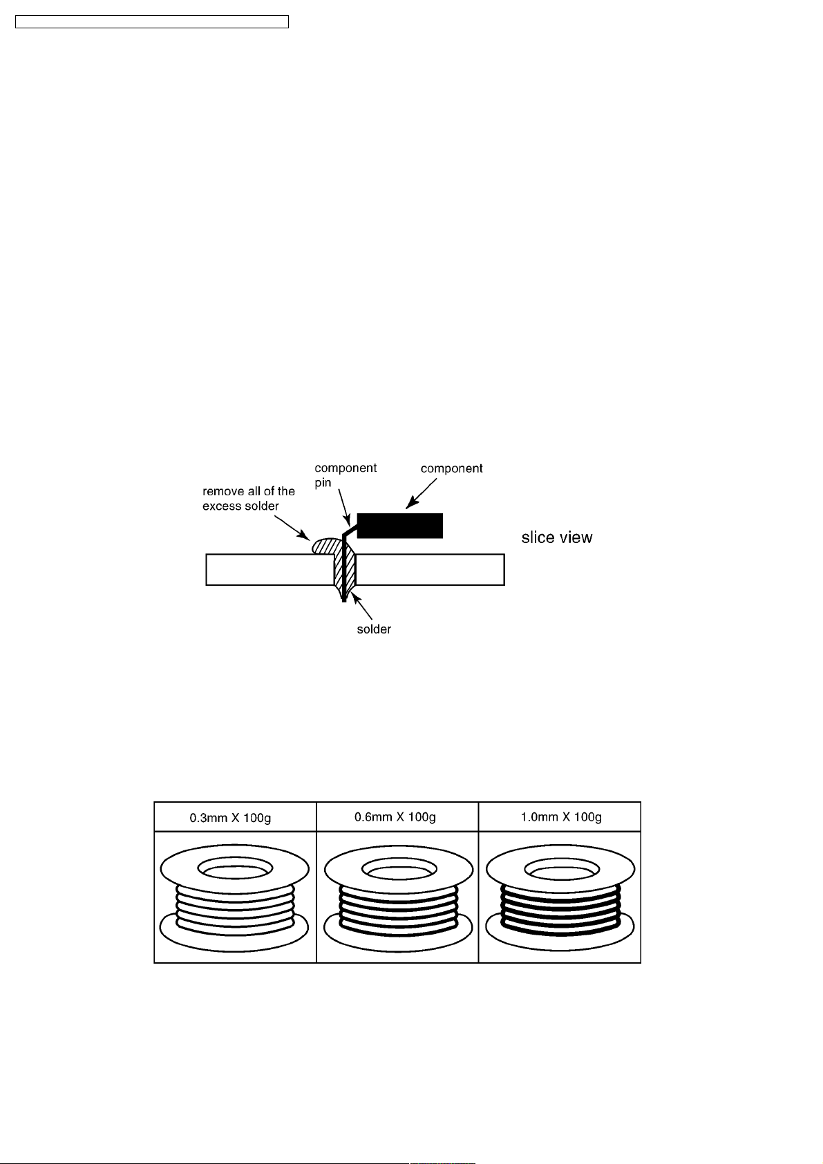
1 ABOUT LEAD FREE SOLDER (PbF: Pb free)
Note:
In the information below, Pb, the symbol for lead in the periodic table of elements, will refer to standard solder or solder that
contains lead.
We will use PbF solder when discussing the lead free solder used in our manufacturing process which is made from Tin (Sn),
Silver (Ag), and Copper (Cu).
This model, and others like it, manufactured using lead free solder will have PbF stamped on the PCB. For service and repair
work we suggest using the same type of solder although, with some precautions, standard Pb solder can also be used.
Caution
•
• PbF solder has a melting point that is 50°F ~ 70° F (30°C ~ 40°C) higher than Pb solder. Please use a soldering iron with
• •
temperature control and adjust it to 700°F ± 20° F (370°C ± 10°C). In case of using high temperature soldering iron, please
be careful not to heat too long.
•
• PbF solder will tend to splash if it is heated much higher than its melting point, approximately 1100°F (600°C).
• •
•
• If you must use Pb solder on a PCB manufactured using PbF solder, remove as much of the original PbF solder as possible
• •
and be sure that any remaining is melted prior to applying the Pb solder.
•
• When applying PbF solder to double layered boards, please check the component side for excess which may flow onto the
• •
opposite side (See the figure below).
1.1. Suggested PbF Solder
There are several types of PbF solder available commercially. While this product is manufactured using Tin, Silver, and Copper
(Sn+Ag+Cu), you can also use Tin and Copper (Sn+Cu), or Tin, Zinc, and Bismuth (Sn+Zn+Bi). Please check the
manufacturer’s specific instructions for the melting points of their products and any precautions for using their product with other
materials.
The following lead free (PbF) solder wire sizes are recommended for service of this product: 0.3mm, 0.6mm and 1.0mm.
4
KX-TG282 0LAB / KX-TG2822L AB / KX-TGA243L AB / KX-TGA2 46LAB
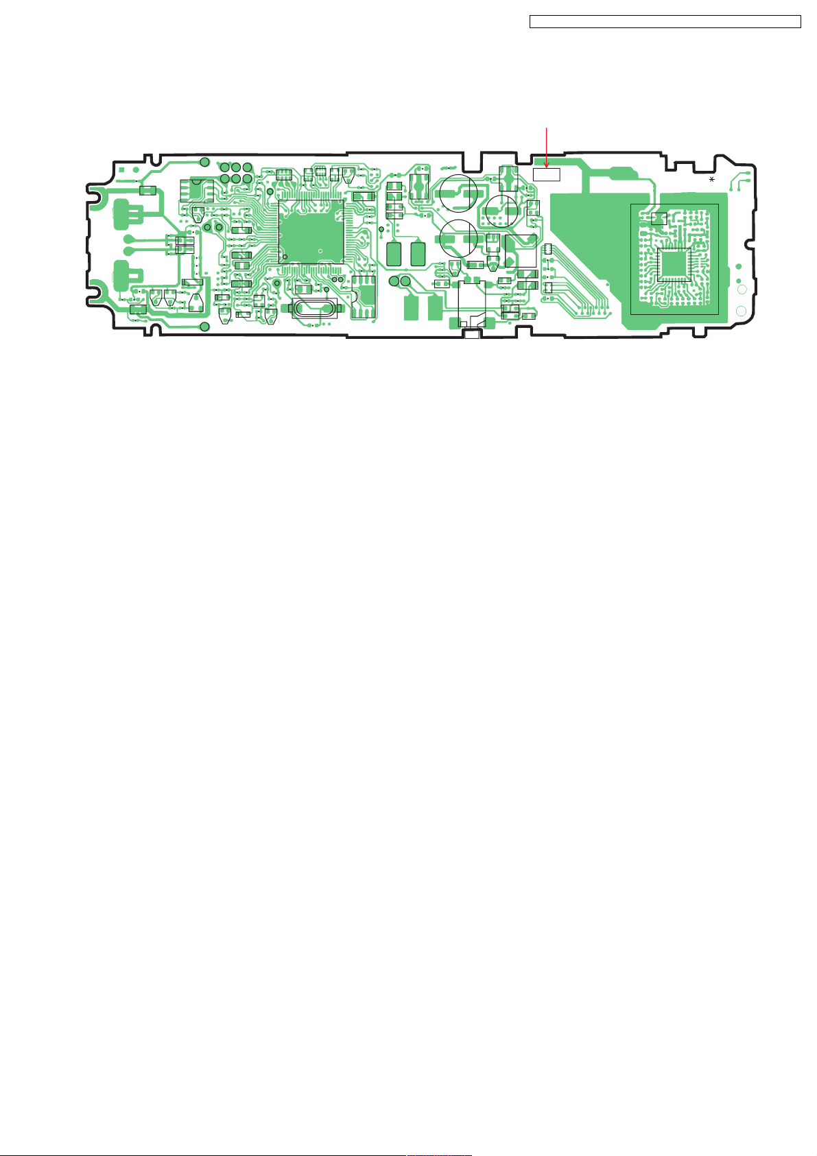
1.2. How to Recognize that Pb Free Solder is Used
(Example: Handset P.C.B.)
Marked
VBATT
R376
R352
C353
L351
R377
R351
JTAG
R243
R231
TX
C209
RX
R207
R206
VSSVSS
C241
R209
R205
R241
5
R226
C244
C226
C243
C377
C303
C304
C315
R315
C316
R317
R314
C314
C317
R312
R318
C208
R334
C336
C305
C333
R333
C307
R228
C231
C306
R208
C222
R222
D231
IC221
R232
Q231
C221
R223
D223
C223
CHG2
1
L352
C313
C311
C312
Q362
R242
C242
Q363
R362
R361R363
R354
C354
D313
D312
R368
R367
R366
R364
IC241
D361
Q361
Q243
R230
CHG1
C206
R340
100
Q221
76
C340
TEST
R224
C224
RA201
75
C202
Q251 Q252 Q253
RA251
R251 R252
IC201
TXO
C212C215C201
R225
C219
C214
RESET
C225
X201
R201
51
251
MOE
R258 R261
R257
R256
C205
50
26
C246
1
C204
R204
R203
RSSI
R234
R249
5
IC249
L211
L326
L327
D326
D327
(Component View)
Note:
The location of the “PbF” mark is subject to change without notice.
C371
IC371
C372
SP_PHONE
RECEIVER
C361
1
R331
R332
C332
L332
C211
C373
Q331
CN331
D373
C384
IC373
Q373
C334
C381
R324
C322
IC381
L334
D324
D323
L373
C335
C321
R325
R323
L331
C382
1
C383
PbF
IC374
C227
R227
CA274
C273
R273
R272
C272
CA271
ANT
SHIELD
PQUP11285Z
FL901
IC901
A
2 FOR SERVICE TECHNICIANS
ICs and LSIs are vulnerable to static electricity.
When repairing, the following precautions will help prevent recurring malfunctions.
1. Cover plastic parts boxes with aluminum foil.
2. Ground the soldering irons.
3. Use a conductive mat on worktable.
4. Do not grasp IC or LSI pins with bare fingers.
3 CAUTION
1. Danger of explosion if battery is incorrectly replaced.
2. Replace only with the same or equivalent type recommended by the manufacturer.
3. Dispose of used batteries according to the manufacturer´s Instructions.
5

KX-TG282 0LAB / KX-TG2822L AB / KX-TGA243L AB / KX-TGA2 46LAB
4 OPERATING INSTRUCTIONS
4.1. Battery
4.1.1. Battery Installation
4.1.2. Battery Charge
4.1.3. Recharging the Battery
Note for service:
The battery strength may not be indicated correctly if the battery is disconnected and connected again, even after it is fully
charged. In that case, by recharging the battery as mentioned above, you will get a correct indication of the battery strength.
4.1.4. Battery Strength
6

4.1.5. Battery Replacement
KX-TG282 0LAB / KX-TG2822L AB / KX-TGA243L AB / KX-TGA2 46LAB
4.1.6. Battery Performance
7
KX-TG282 0LAB / KX-TG2822L AB / KX-TGA243L AB / KX-TGA2 46LAB
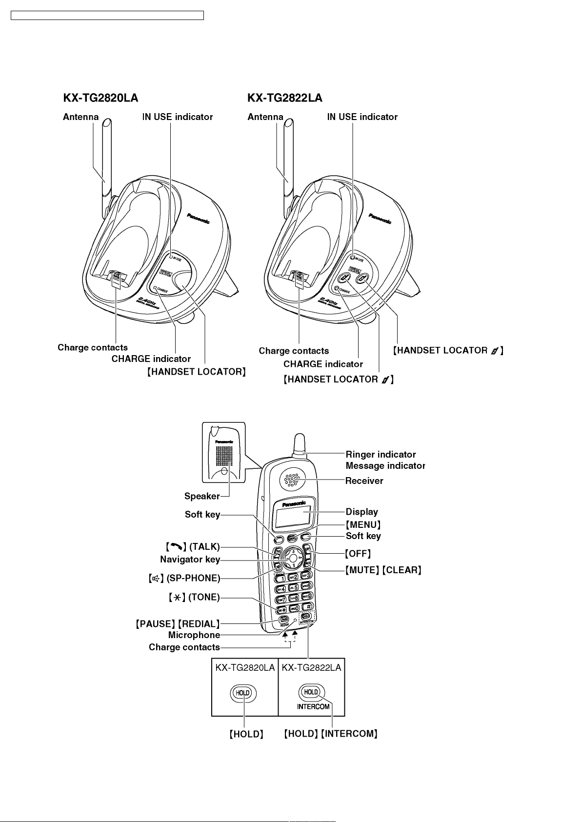
4.2. Location of Controls
4.2.1. Base Unit
4.2.2. Handset
8
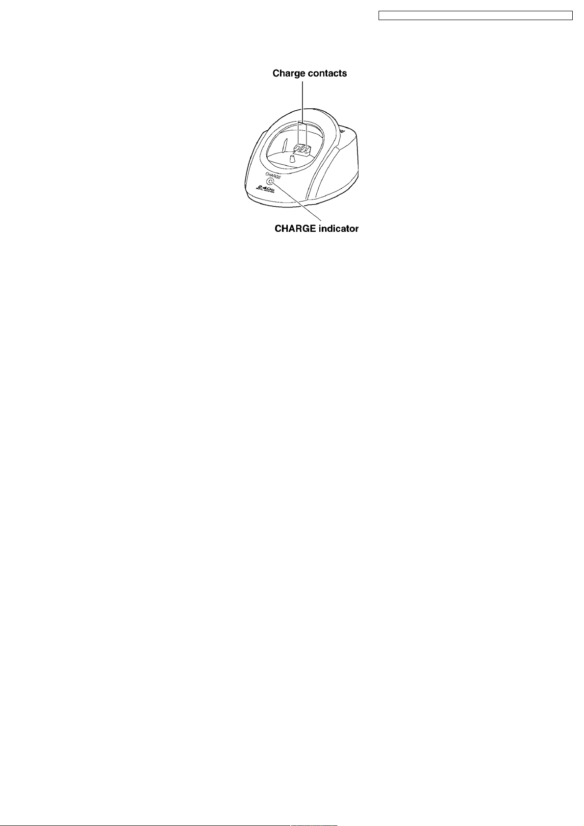
4.2.3. Charger Unit (KX-TG2822LA only)
KX-TG282 0LAB / KX-TG2822L AB / KX-TGA243L AB / KX-TGA2 46LAB
9

KX-TG282 0LAB / KX-TG2822L AB / KX-TGA243L AB / KX-TGA2 46LAB
4.3. Displays
4.3.1. Display Items
4.3.2. Troubleshooting (Handset LCD)
10

4.4. Settings
4.4.1. Connections
KX-TG282 0LAB / KX-TG2822L AB / KX-TGA243L AB / KX-TGA2 46LAB
11

KX-TG282 0LAB / KX-TG2822L AB / KX-TGA243L AB / KX-TGA2 46LAB
12

4.4.2. Guide to Handset Programming
KX-TG282 0LAB / KX-TG2822L AB / KX-TGA243L AB / KX-TGA2 46LAB
13

KX-TG282 0LAB / KX-TG2822L AB / KX-TGA243L AB / KX-TGA2 46LAB
4.4.3. Direct Commands
14

KX-TG282 0LAB / KX-TG2822L AB / KX-TGA243L AB / KX-TGA2 46LAB
4.5. Troubleshooting
If the handset display shows error messages, see “Troubleshooting (Handset LCD) (P.10)” for the Cause & Solution.
15

KX-TG282 0LAB / KX-TG2822L AB / KX-TGA243L AB / KX-TGA2 46LAB
16

KX-TG282 0LAB / KX-TG2822L AB / KX-TGA243L AB / KX-TGA2 46LAB
17
KX-TG282 0LAB / KX-TG2822L AB / KX-TGA243L AB / KX-TGA2 46LAB
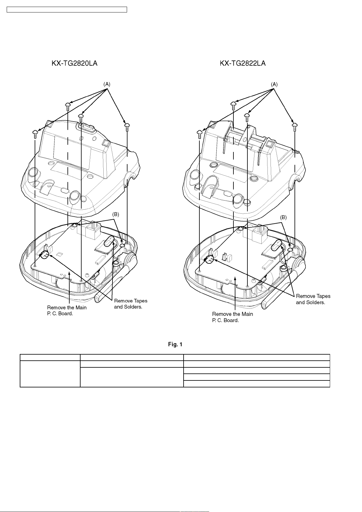
5 DISASSEMBLY INSTRUCTIONS
5.1. Base Unit
Shown in Fig.- To Remove - Remove -
1 Cabinet Cover Screws (2.6 × 12).....(A) × 4
Main P. C. Board Screws (2.6 × 8).......(B) × 2
Tapes and Solders
Main P. C. Board
18

5.2. Handset
KX-TG282 0LAB / KX-TG2822L AB / KX-TGA243L AB / KX-TGA2 46LAB
Shown in Fig.- To Remove - Remove -
2 Cabinet Cover Screws (2 × 10).............(C) × 2
3 Follow the procedure.
4 Main P. C. Board Tape and Solders
Screws (2 × 10).............(D) × 3
Charge Terminals
Main P. C. Board
19

KX-TG282 0LAB / KX-TG2822L AB / KX-TGA243L AB / KX-TGA2 46LAB
5.3. Charger Unit
Shown in Fig.- To Remove - Remove -
5 Cabinet Cover Screws (2.6 × 12).............( E) × 2
Main P. C. Board Solders
Main P. C. Board
20

KX-TG282 0LAB / KX-TG2822L AB / KX-TGA243L AB / KX-TGA2 46LAB
6 HOW TO REPLACE THE HANDSET LCD
21

KX-TG282 0LAB / KX-TG2822L AB / KX-TGA243L AB / KX-TGA2 46LAB
7 TROUBLESHOOTING GUIDE
Cross Reference:
Check Power (P.23)
Check Battery Charge (P.24)
Check Link (P.25)
Check the RF part (P.26)
Check Handset Transmission (P.33)
Check Handset Reception (P.33)
Check Caller ID (P.33)
22

7.1. Check Power
KX-TG282 0LAB / KX-TG2822L AB / KX-TGA243L AB / KX-TGA2 46LAB
Cross Reference:
Power Supply Circuit (P.54)
Reset Circuit (P.56)
Note:
DSP is IC501.
23

KX-TG282 0LAB / KX-TG2822L AB / KX-TGA243L AB / KX-TGA2 46LAB
7.2. Check Battery Charge
Note:
DSP is IC501.
24

7.3. Check Link
KX-TG282 0LAB / KX-TG2822L AB / KX-TGA243L AB / KX-TGA2 46LAB
Note:
DSP is IC501.
(*1) Refer to Finding out the Defective part (P.26).
Cross Reference:
Check the RF part (P.26)
25

KX-TG282 0LAB / KX-TG2822L AB / KX-TGA243L AB / KX-TGA2 46LAB
7.4. Check the RF part
7.4.1. Finding out the Defective part
After All the Checkings or Repairing
1. Re-register the checked Handset to the checked Base Unit, and Regular HS to Regular BU.
Note:
(*1) HS: Handset
(*2) BU: Base Unit
26

7.4.1.1. Re-registering the Handset
KX-TG282 0LAB / KX-TG2822L AB / KX-TGA243L AB / KX-TGA2 46LAB
27

KX-TG282 0LAB / KX-TG2822L AB / KX-TGA243L AB / KX-TGA2 46LAB
7.4.2. RF Check Flowchart
Each item (1 ~ 6) of RF Check Flowchart corresponds to Check Table for RF part (P.29).
Please refer to the each item.
28

KX-TG282 0LAB / KX-TG2822L AB / KX-TGA243L AB / KX-TGA2 46LAB
7.4.3. Check Table for RF part
No. Item BU (Base Unit) Check HS (HandSet) Check
1 Link Confirmation Normal
HS, BU Mode [Normal Mode]
2 Control signal confirmation
HS, BU Mode: [Test Burst Mode] (*1)
3 X’tal Frequency confirmation (*7)
HS, BU Mode: [Adjustment] (*3)
4 TX Power confirmation
Regular HS, BU Mode:
[RX-CW Mode.] (*4)
HS, BU (to be checked) Mode:
[Test Burst Mode.] (*1)
5 RX Sensitivity confirmation
Regular HS, BU Mode:
[Test Burst Mode.] (*1)
HS, BU (to be checked) Mode:
[RX-CW Mode.] (*4)
6 Range Confirmation Normal
HS, BU Mode: [Normal Mode]
1. Register Regular HS to BU (to be checked).
2. Press [Talk] key of the Regular HS to
establish link.
Check DSP interface. (*2) Check DSP interface. (*2)
Check X’tal Frequency.
(13.824000MHz ±100Hz)
1. Place the Regular HS about 15cm away
from the BU.
2. Confirm that RSSI of the Regular HS is
approximately 2V by Oscilloscope. (*5)
1. Place the Regular HS about 15cm away
from the BU.
2. Confirm that RSSI of the BU is
approximately 2V by Oscilloscope. (*5)
1. Register Regular HS to BU (to be checked).
2. Press [Talk] key of the Regular HS to
establish link.
3. Compare the range of the BU (being
checked) with that of the Regular BU.
1. Register HS (to be checked) to Regular BU.
2. Press [Talk] key of the HS to establish link.
Check X’tal Frequency.
(13.824000MHz ±100Hz)
1. Place the HS about 15cm away from the
Regular BU.
2. Confirm that RSSI of the Regular BU is
approximately 2V by Oscilloscope. (*6)
1. Place the HS about 15cm away from the
Regular BU.
2. Confirm that RSSI of the HS is
approximately 2V by Oscilloscope. (*6)
1. Register HS (to be checked) to Regular BU.
2. Press [Talk] key of the HS to establish link.
3. Compare the range of the HS (being
checked) with that of the Regular HS.
Note:
(*1)(*3)(*4) ADJUSTMENT AND TEST MODE (P.34)
(*2) RF-DSP Interface Signal Wave Form (P.31)
(*5) Base Unit Reference Drawing (P.43)
(*6) Handset Reference Drawing (P.44)
(*7) X501 (Base Unit), X201 (Handset) Check (P.42)
29

KX-TG282 0LAB / KX-TG2822L AB / KX-TGA243L AB / KX-TGA2 46LAB
7.4.4. TEST RANGE Check
Circuit block which range is defective can be found by the following check.
Item BU (Base Unit) Check HS (HandSet) Check
Range Confirmation TX
TEST
(TX Power check)
HS, BU Mode:
[Test Link Mode] (*1)
1. Register Regular HS to BU (to be checked).
2. Set BU to “Test Link mode”.
3. Set Regular HS to “Test Link mode”.
*Set TX Power and RX Sensitivity of the BU and the
Regular HS by CHART1.
1. Register HS (to be checked) to Regular BU.
2. Set Regular BU to “Test Link mode”.
3. Set HS to “Test Link mode”.
*Set TX Power and RX Sensitivity of the HS and the
Regular BU by CHART1.
Range Confirmation RX
TEST
(RX sensitivity check)
HS, BU Mode:
[Test Link Mode] (*1)
* At distance of about 20m between HS and BU,
Link OK = TX Power of the BU is OK.
No Link = TX Power of the BU is NG.
1. Register Regular HS to BU (to be checked).
2. Set BU to “Test Link mode”.
3. Set Regular HS to “Test Link mode”.
*Set TX Power and RX Sensitivity of the BU and
Regular HS by CHART1.
* At distance of about 20m between HS and BU,
Link OK= RX Sensitivity of the BU is OK.
No Link = RX Sensitivity of the BU is NG.
* At distance of about 20m between HS and BU,
Link OK = TX Power of the HS is OK.
No Link = TX Power of the HS is NG.
1. Register HS (to be checked) to Regular BU.
2. Set Regular BU to “Test Link mode”.
3. Set HS to “Test Link mode”.
* Set TX Power and RX Sensitivity of Checking_HS
and Regular_BU by CHART1.
* At distance of about 20m between HS and BU,
Link OK= RX Sensitivity of the HS is OK.
No Link = RX Sensitivity of the HS is NG
CHART1: Setting of TX Power and RX Sensitivity in Range Confirmation TX TEST, RX TEST
BU (to be checked) Regular_HS
TX Power RX Sens. TX Power RX Sens.
BU (Base Unit) TX Power Check High High High Low
BU (Base Unit) RX Sensitivity Check High High Low High
HS (to be checked) Regular_BU
TX Power RX Sens. TX Power RX Sens.
HS (Handset) TX Power Check High High High Low
HS (Handset) RX Sensitivity Check High High Low High
Note:
(*1) ADJUSTMENT AND TEST MODE (P.34)
30
 Loading...