Hologram Unit
,,
,,
,,
,,
,
,,,
,,
,
HUL7207
Hologram Unit
For optical information processing
Features
Smaller package size achieved through
micro-mirror integration
(4.8 × 8.2 × 4.3 mm)
Fast response (fC = 50 MHz)
Focus error signal detection : SSD method
Tracking error signal detection
: 3-beam method
Low-power semiconductor laser included
Applications
CD-ROM drives
(supports 40 time speed CD-ROM drives)
Absolute Maximum Ratings (Ta = 25˚C)
Parameter Symbol Ratings Unit
Laser beam output
Laser reverse voltage V
Monitor PD reverse voltage
Supply voltage V
Operating supply voltage range
Reference voltage V
Operating ambient temperature
Storage temperature T
*1
Light emitting output through objective lens
*1
V
P
O
R(LD)
R(mon)
CC
V
CC
C
T
opr
stg
+3.0 to +5.5 V
+1.3 to V
– 10 to +60 ˚C
– 40 to +85 ˚C
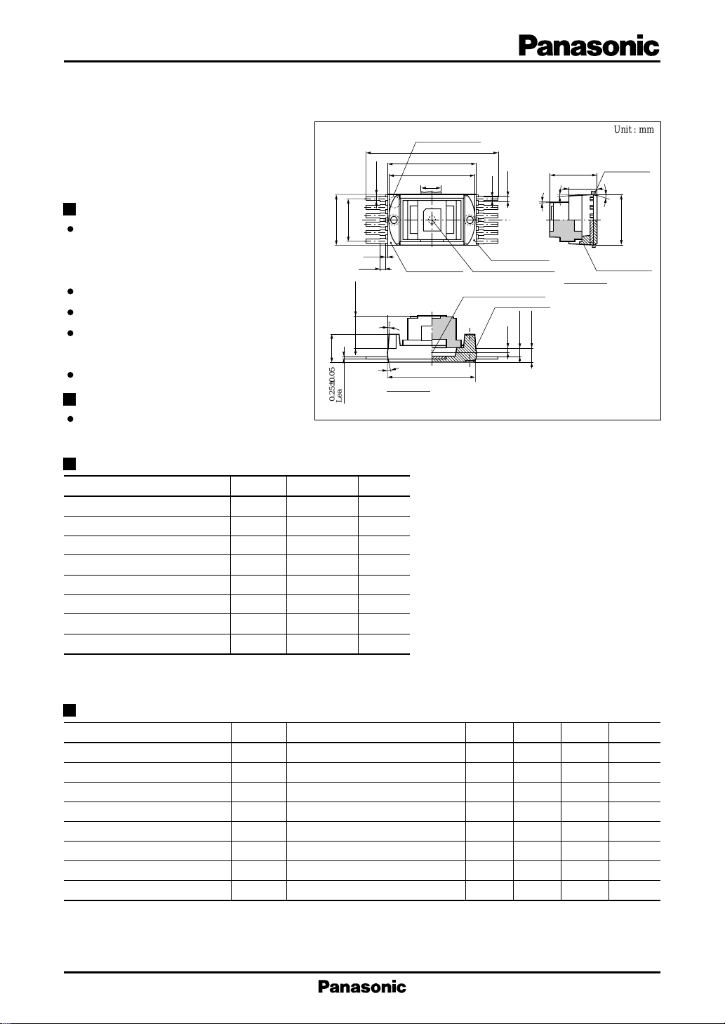
Index mark for No.1
pin on reverse side
11.2±0.2
8.2±0.2
ø8.0
Reference plane
2˚
7˚
SEC. X-O-Y
(1.8)
8.1±0.2
4.8±0.1
2.55±0.2
0.25±0.05
Lead frame
0.8×5=4.0
3.0±0.2
1
2
3
4
5
6
(0.2)
(0.5)
0.4±0.1
0.3 mW
2V
6V
6V
–1.3
CC
V
+0
–0.05
(0.35)
(0.3)
12
11
10
X
O
Y
(Note): 1.Standard corner R=0.20 max.
2.Thickness of plate:Ni 1µm min.+Au 0.1µm min.
3.Thickness of hologram=2.0mm, n=1.519
9
8
7
Reference plane
Apparent emitting point
Apparent emitting point
Reference plane
0.50
4.33±0.2
2.55±0.2
3˚
2˚
SEC. X-O-Y
1.33±0.2
0.78±0.2
Unit : mm
Gate the rest
7˚
4.7±0.1
Position of
reference plane
Unit Characteristic Specifications (Tc = 25±3˚C)
Parameter Symbol Conditions min typ max Unit
Laser beam output
Operating current I
Operating voltage V
Oscillating wavelength λ
Focus error signal amplitude
Tracking error signal amplitude
Focus error signal pull-in range
Frequency characteristics f
*1
Light emitting output through objective lens
*1
P
O
OP
OP
L
V
FE
V
TE
D
FE
C
VRF = 570mV, VCC = 5V 0.18 0.25 mW
CW VRF = 570mV, VCC = 5V 25 35 45 mA
CW VRF = 570mV, VCC = 5V 1.9 2.4 V
VRF = 570mV, VCC = 5V 775 795 815 nm
VRF = 570mV, VCC = 5V 340 480 620 mV
VRF = 570mV, VCC = 5V 220 340 460 mV
VRF = 570mV, VCC = 5V 9 12 16 µm
40 50 MHz
1

Hologram Unit HUL7207
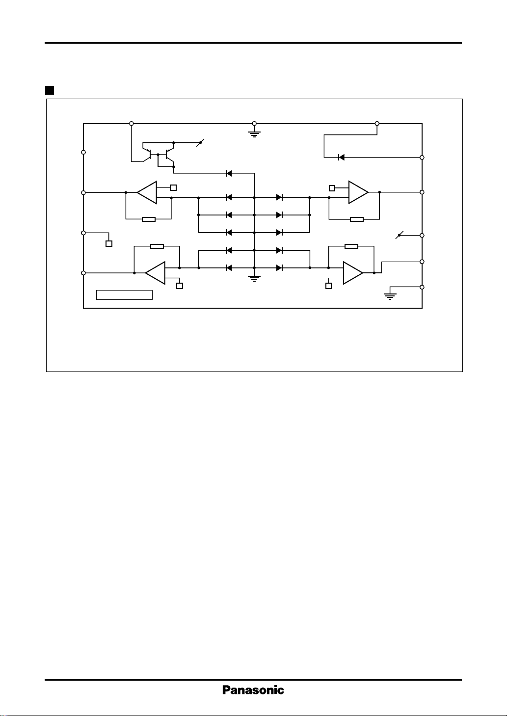
Block Diagram of Circuit Functions
1122
3
4
+
–
5
6
BAND GAP Reg.
–
+
LD
11
Pmon
P2
P4
P8
P3
P7
P9
+
–
10
9
P1
P6
P5
P10
–
+
8
7
1: GND
2: Mon. out
3: N.C.
4: (P2+P4+P8) out
5: V
C
6: (P1+P6) out
7: GND
8: (P5+P10) out
9: V
CC
10: (P3+P7+P9) out
11: LD (+)
12: LD (–)
2
 Loading...