Panasonic HUL7001 Datasheet

Hologram Unit
,,
,,
HUL7001
Hologram Unit
For optical information processing
Features
Smaller package size achieved through
micro-mirror integration
(4.8 × 8.2 × 4.3 mm)
Focus error signal detection : SSD method
Tracking error signal detection
: 3-beam method
Low-power semiconductor laser included
Applications
CD
Absolute Maximum Ratings (Ta = 25˚C)
Parameter Symbol Ratings Unit
Laser beam output P
Laser reverse voltage V
Monitor PD reverse voltage V
Signal processing PD reverse voltage
Operating ambient temperature
Storage temperature T
O
R(LD)
R(mon)
V
R
T
opr
stg
– 10 to +60 ˚C
– 40 to +85 ˚C
1
2
3
4
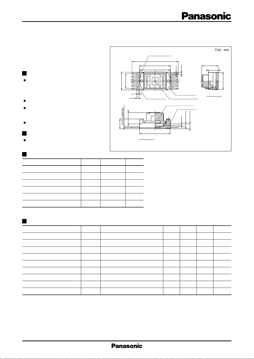
4.8±0.1
5
6
0.8×5=4.0±0.2
(0.2)
(0.5)
3.0±0.2
0.25 Lead frame
2.55±0.2
Reference plane
SEC. X-O-Y
0.3 mW
2V
12 V
12 V
Index mark for No.1
pin on reverse side
11.2±0.2
8.2±0.2
+0
ø8.0
–0.05
O
Y
8.1±0.2
(Note): 1.Standard corner R=0.20 max.
2.Thickness of plate:Ni 1µm min.+Au 0.1µm min.
3.Thickness of hologram=2.0mm, n=1.519
(0.35)
(0.3)
12
11
10
X
9
8
7
Reference plane
Apparent emitting point
Apparent emitting point
Reference plane
1.33±0.2
0.78±0.2
0.50
Unit : mm
4.33±0.2
2.55±0.2
4.7±0.1
SEC. X-O-Y
Unit Characteristic Specifications (Tc = 25 ± 3˚C)
Parameter Symbol Conditions min typ max Unit
Threshold current I
Operating current I
Operating voltage V
Laser beam output P
Focus error signal amplitude
Tracking error signal amplitude
Focus error signal defocusing
Tracking error signal symmetry
Focus error signal pull-in range
*1
Measurements are made using the reference optical system during measurement and the radiant power measurement system on
the hologram unit shown in Fig. 2.
*2
It should be noted that the RF signal amplitude in these specifications is denoted by IRF, and represents the amplitude of the 11T
signal. As in the case described in *1, IRF is measured using the measurement system shown in Fig. 2.
*3
The definition is illustrated in Fig. 3.
*4
The definition is illustrated in Fig. 4.
*5
The definition is illustrated in Fig. 5.
*1
th
OP
OP
O
I
FE
I
TE
D
FO
B
TE
D
FE
CW 20 30 40 mA
*1,2
CW IRF = 10µA, VR = 5V 25 35 45 mA
*1,2
CW IRF = 10µA, VR = 5V 1.9 2.4 V
*1,2
IRF = 10µA, VR = 5V 0.15 0.22 mW
*1,3
IRF = 10µA, VR = 5V 7 10 13 µ A
*1,4
IRF = 10µA, VR = 5V 0.8 1.3 1.8 µA
*1,5
IRF = 10µA, VR = 5V – 8 + 8 %
*1,4
IRF = 10µA, VR = 5V – 30 + 30 %
*1,3
IRF = 10µA, VR = 5V 12 µm
1

HUL7001 Hologram Unit
Characteristic Specifications for Semiconductor Laser, Monitor PD, and Signaling Processing PD
Parameter Symbol Conditions min typ max Unit
Semiconductor laser
Oscillating wavelength λ
Coherence λ
Monitor PD and signal processing PD
Monitor current I
Dark current
Capacitance between pinss
Shield frequency f
*6
Measurements are made using the radiant power measurement system on the hologram unit. The definition is presented in Fig. 2.
*7
Unless otherwise indicated, the values shown are per individual element.
*8
The subscript (mon) denotes the element (monitor PD).
*9
C
denotes the capacitance measured at pin No. 4 or 10 in the electrode connection diagram. C
t(RF1)
measured at pin No. 5 or 9 in the electrode connection diagram.
*6
L
P(mon)
I
I
D(mon)
C
t(RF1)
C
t(RF2)
CW IRF = 10µA, VR = 5V 775 790 805 nm
*6
CW IRF = 10µA, VR = 5V 0.5 0.9
*7
CW IRF = 10µA, VR = 5V 0.3 0.7 1.2 mA
VR = 2.5V 0.2 3.0 nA
D
*8
VR = 5V 0.3 30 nA
*9
VR = 2.5V, f = 1MHz
*9
VR = 2.5V, RL = 50Ω 40 MHz
C
(Tc = 25±3˚C)
2pF
3pF
denotes the capacitance
t(RF2)
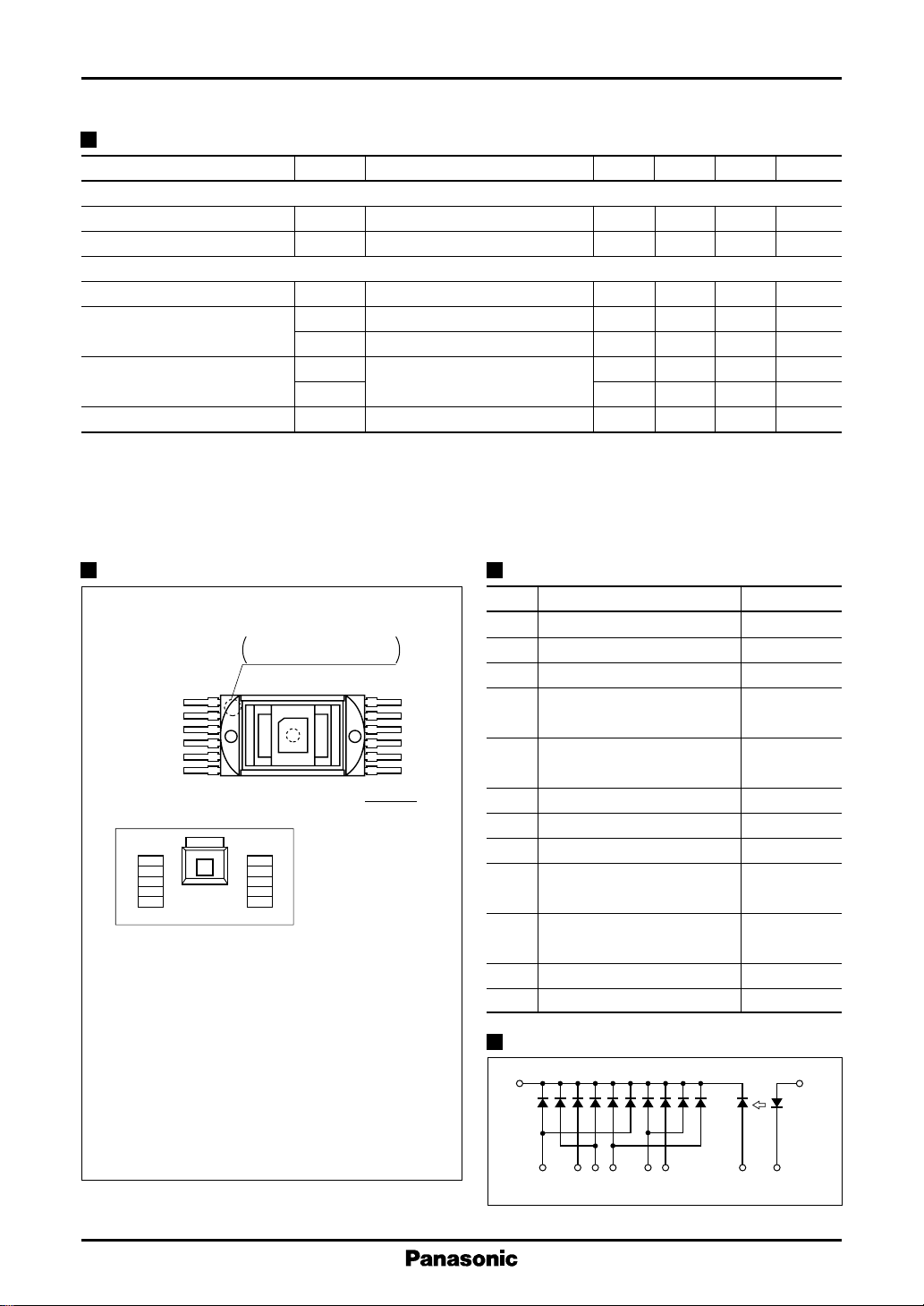
Connection Diagram (Fig. 1)
(a) Pin arrangement
Pin No.
(b) Chip structure
PD output current In :
detecting element N (n : 1 to 10, N = P1 to P10 )
Monitor PD output current I
received by Pmon element
Focus error signal FE = (I
Tracking error signal TE = (I
RF signal RF = I2+I3+I4+I7+I8+I
1
2
3
4
5
6
Pmon
P1
LD
P2
P3
P4
P5
Output current when light is received by light
Gritty face
Represents No.1 pin
carved seal on reverse side
TOP VIEW
LD
:
P6
P7
P8
P9
P10
: Output current when light is
P (mon)
2+I4+I8
Disk-close FE > 0
Disk-far FE < 0
1+I6
The leading beam is the beam received
by light detecting elements P1 and P6.
Semiconductor laser chip
: Monitor light detecting
Pmon
element
P1 ~ P10
: Signal-detection light detecting-elements
) – (I3+I7+I9)
) – (I5+I10)
9
12
11
10
9
8
7
Pin Description
Pin No.
1
Source voltage Applications pin
2 Monitor current output pin I
3
Tracking error signal output pin
RF and focus error signal
4
output pin
RF and focus error signal
5
output pin
6
Source voltage Applications pin
7
Source voltage Applications pin
8
Tracking error signal output pin
RF and focus error signal
9
output pin
RF and focus error signal
10
output pin
11 LD + Power supply pin
12 GND pin
Function Calculation
Electrode Connection Diagram
1,6,7
P1 P2 P3 P4 P5 P6 P7 P8 P9
)
(V
R
348910 2125
Pmon LD
P10
P (mon)
I1 + I
I
I2 + I
I5 + I
I7 + I
I
GND
6
3
4
10
9
8
11
LD+
2
 Loading...